ATAK5753-43P3-S中文资料
TG-3530SA;中文规格书,Datasheet资料
13. 12. 11. 10.
tr tf t_str
N.C. N.C. N.C.
7.40.2
3.20.1
9. 8.
3.0sMax.
1)
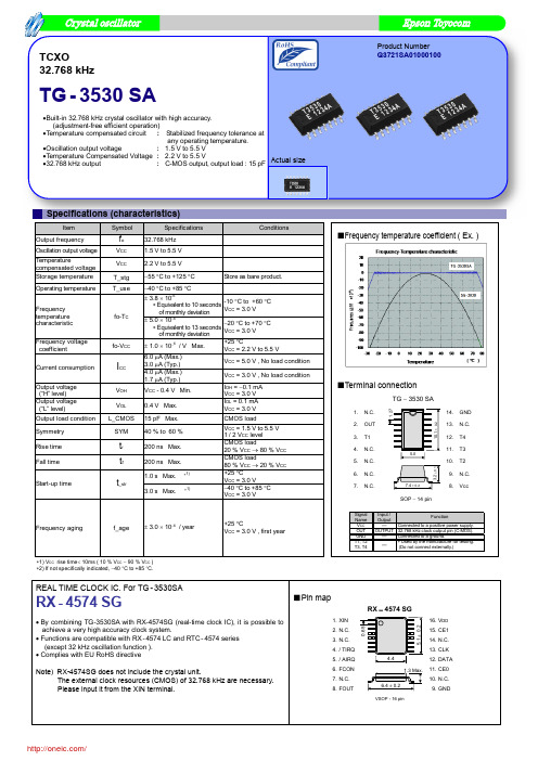
SOP14 pin
Signal Name VCC OUT GND T1,T2 T3,T4 Input / Function Output Connected to a positive power supply. OUTPUT 32.768kHzclock output pin (C-MOS). Connected to a ground. Used by the manufacture for testing. (Do not connect externally.)
15. CE1 14. N.C. 13. CLK 12. DATA 11. CE0 10. N.C. 9. GND
Note) RX-4574SG does not include the crystal unit. The external clock resources (CMOS) of 32.768 kHz are necessary. Please input it from the XIN terminal.
1)
Conditions
fo
VCC VCC T_stg T_use
■Frequency temperature coefficient(Ex.)
Store as bare product.
-10Cto +60C VCC=3.0V 20Cto+70C VCC=3.0V +25C VCC=2.2Vto5.5 V VCC=5.0V,No load condition VCC=3.0V,No load condition IOH=0.1mA VCC=3.0V IOL=0.1mA VCC=3.0V CMOS load VCC=1.5Vto5.5 V 1/2VCC level CMOS load 20%VCC80%VCC CMOS load 80%VCC20%VCC +25C VCC=3.0V 40Cto+85C VCC=3.0V
家电维修-TCL-CRT背投电视介绍

技术前沿
T C L - C R T 背投电视介绍 下
李培仁
5.CRT 背投的信号流程 TCL-CRT 背投目前所用的机心主要 有以下四种 HiD435B.r机心 属60Hz逐 行扫描机心 HiD432机心 属低价60Hz 逐行扫描机心 HiD438SB.r 属85Hz逐 行扫描机心 HiD43P9机心 属100Hz逐 行扫描机心 1 HiD435B.r HiD435B.r 机心采用 PHILIPS 的 TDA9321 电视信号解调和 TDA9332 显示 处理芯片 nDSP 公司的 NV320 逐行处理 芯片 实现 60Hz 逐行扫描 CPU 芯片为 东芝 TMP87PS38 在生产批量不大时使 用 OTP 方式将软件烧写到芯片上 便于 根据生产和市场反馈有可能对软件作修 改 画中画功能板 会聚功能板均设计成 有屏蔽罩的模块形式 其中会聚模块每 机必有 画中画模块可随机型功能的变 化选配 HiD435B.r机心将普通电视扫描行数 加倍 PAL制可支持60Hz数字逐点成像 画面不闪烁 图像更细腻 清晰 无行结 构线 可连接 PC 以电脑画面玩休闲软 件 游玩网络世界 支持 VGA 640 480/60Hz HiD435B.r主板流程图如图6所示
CS5755AT 三相全桥智能功率模块说明书
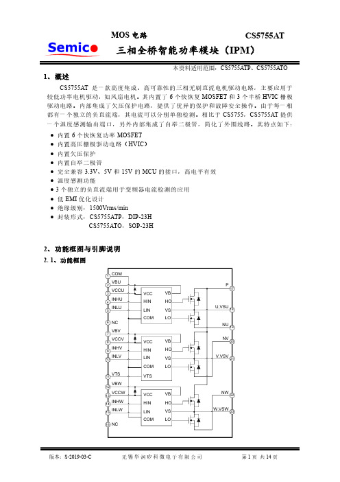
MOS电路CS5755AT三相全桥智能功率模块(IPM)1、概述CS5755AT是一款高度集成、高可靠性的三相无刷直流电机驱动电路,主要应用于较低功率电机驱动,如风扇电机。
其内置了6个快恢复MOSFET和3个半桥HVIC栅极驱动电路。
内部集成了欠压保护电路,提供了优异的保护和故障安全操作。
由于每一相都有一个独立的负直流端,其电流可以分别单独检测。
相比于CS5755,CS5755AT提供一个温度感测输出端口,另外内部集成了自举二极管,简化了外围线路。
其特点如下:●内置6个快恢复功率MOSFET●内置高压栅极驱动电路(HVIC)●内置欠压保护●内置自举二极管●完全兼容3.3V、5V和15V的MCU的接口,高电平有效●温度感测功能● 3个独立的负直流端用于变频器电流检测的应用●低EMI优化设计●绝缘级别:1500Vrms/min● 封装形式:CS5755ATP:DIP-23HCS5755ATO:SOP-23H2、功能框图与引脚说明2. 1、功能框图2. 2、功能描述该电路内置了6个快恢复MOSFET 和3个半桥HVIC 栅极驱动电路,如上图所示。
每一个半桥HVIC 栅极驱动电路功能框图及描述如下:该HVIC 栅极驱动主要由高低电平转换器、互锁逻辑、延时逻辑、脉冲发生器、脉冲过滤器、欠压保护逻辑和高低侧端驱动级等模块构成。
LIN 输入信号通过一个由内部稳压供电(门限电压不受外压影响)的施密特触发器后输入给内部稳压-外部低压供电VCC 之间的电平转换,再通过用于控制死区时间的延时电路,最后输入到驱动级。
HIN 输入信号同样通过一个由内部稳压供电的施密特触发器后输入给内部稳压-外部低压供电VCC 间进行电平转换,然后输入延时电路,输出由低压通道欠压保护模块的输出信号控制产生两路固定相位差的定频短脉冲,然后通过VCC-VS 电平转换将脉冲电平变换为VB-VS 之间,再通过脉冲过滤模块,和高压通道欠压保护模块的输出信号一起输入给RS 触发器,最后输出控制高压通道的驱动级。
1.5KE43CA(SynSemi)中文数据手册「EasyDatasheet」
P,D稳态功耗0 0
25
50 75 100 125 150 175 200
TL,引线温度(℃)
图5 -脉冲波形
RMS Tr = 10µs
100
Peak Value
IRMS
TJ=25 °C Pulse Width (tp) is defined as that point where the peak current decays to 50% of IRSM
94.0
1.5KE120A 1.5KE120CA
114
126
1.0
102
1.5KE130A 1.5KE130CA
124
137
1.0
111
1.5KE150A 1.5KE150CA
143
158
1.0
128
1.5KE160A 1.5KE160CA
152
168
1.0
136
1.5KE170A 1.5KE170CA
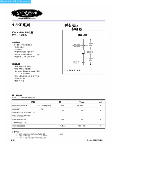
瞬态电压 抑制器
DO-201
0.21 (5.33) 0.19 (4.83)
0.052 (1.07) 0.048 (0.97)
1.00 (25.4) MIN.
0.375 (9.53) 0.285 (7.24)
1.00 (25.4) MIN.
尺寸以英寸(毫米)
最大额定值
等级25
°C 环境温度,除非另有规定.
1.0
25.6
1.5KE33A
1.5KE33CA
31.4
34.7
1.0
28.2
1.5KE36A
1.5KE36CA
34.2
37.8
1.0
30.8
FNK MOS管型号参数大全

12 10 4.5 4.5 2.8 4.5 4.2 1.8 16 6 20 210 5.5 5 15 6.5 3.3 6.5 5 3.2 22 8 28 350 7 7 20 7 19 17 17 15 21 23 24 24 21 27 24 22 22 20 26 6 3.2 6 5.2 2.3 19 8 27 310 7 7 20
Vcesat(15V) (V) Typ Max
Assembly SOT-23 DFN2X26L SOT-23 SOT-23 SOP8 Double SOP8 Double SOP-8 SOT-23 SOT-23 SOT-23 SOT-23 SOT-23 SOT23-3L SOT-23 SOT23-3L SOT-23 SOP-8 SOP-8 SOP-8 SOP-8 SOP-8 SOP-8 SOP-8 Double SOP-8 TO-252 SOP-8 SOP-8 SOP-8 SOP-8 DFN5X68L TO-251 TO-251 TO-252 TO-220 SOP-8 SOT23-3L SOP-8 SOP-8 TO-252 TO-252 TO-252 TO-252 SOP-8 TO-220 TO-252 TO-220 TO-252 TO-220 TO-220 TO-220 TO-220 TO-220 TO-220 TO-263 TO-220 SOT-23 SOT-23 SOT-23 SOT-23 SOT23-6 Single SOT23-6 Single TSSOP-8 Single TSSOP-8 Single TSSOP-8 Single SOP-8 Single SOP-8 Single SOP-8 Single SOP-8 Double SOP-8 Double SOP-8 SOP8 TO-251 TO-251 TO-252 TO-252 PDFN5*6 TSSOP-8 SOP-8 SOT23 SOT-523 TSSOP-8 SOP-8 TSSOP-8 Single TSSOP-8 Single FDFN3.3*3.3 TSSOP-8 SOT23-6 SOT23-6 SOT23
SA575中文资料
TEST CONDITIONS
SA575
UNITS
MIN
TYP
MAX
For compandor, including summing amplifier
VCC
Supply voltage1
ICC VREF
Supply current Reference voltage2
RL
Summing amp output load
GBW
Bandwidth
ENI PSRR
Input voltage noise Power supply rejection ratio
1kHz, 0dB, CREF = 220µF
RL = 10kΩ 1kHz
VIN = 0.5V to 4.5V
RL = 10kΩ Unity gain Unity gain BW = 20kHz 1kHz, 250mV
VCC +5V
0.1µF
VREF
VOUT
C3
+
10µF
+ CRECT
2.2µF
GND VIN
C6
10µF +
+
10µF
GND
GND
1+
575
20
VCC
2–
OP AMP
+ 19
3
– 18
OP AMP
C15
R13 10k
10µF
+
C14
GND VIN
VREF
4
3.8k
5
Σ
6
7
10k
17
16
3.8k
C11
• 600Ω drive capability • Single or split supply operation • Wide input/output swing capability • 3000V ESD protection
T5754_07中文资料
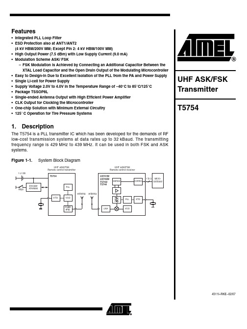
Features Array•Integrated PLL Loop Filter•ESD Protection also at ANT1/ANT2(4kV HBM/200V MM; Except Pin2: 4kV HBM/100V MM)•High Output Power (7.5dBm) with Low Supply Current(9.0mA)•Modulation Scheme ASK/ FSK–FSK Modulation is Achieved by Connecting an Additional Capacitor Between the XTAL Load Capacitor and the Open Drain Output of the Modulating Microcontroller •Easy to Design-in Due to Excellent Isolation of the PLL from the PA and Power Supply •Single Li-cell for Power Supply•Supply Voltage 2.0V to 4.0V in the Temperature Range of –40°C to 85°C/125°C •Package TSSOP8L•Single-ended Antenna Output with High Efficient Power Amplifier•CLK Output for Clocking the Microcontroller•One-chip Solution with Minimum External Circuitry•125°C Operation for Tire Pressure Systems1.DescriptionThe T5754 is a PLL transmitter IC which has been developed for the demands of RF low-cost transmission systems at data rates up to 32kBaud. The transmitting frequency range is 429MHz to 439MHz. It can be used in both FSK and ASK systems.Figure 1-1.System Block Diagram24511I–RKE–02/07T57542.Pin ConfigurationFigure 2-1.Pinning TSSOP8L34511I–RKE–02/07T5754Figure 2-2.Block Diagram44511I–RKE–02/07T57543.General DescriptionThis fully integrated PLL transmitter allows particularly simple, low-cost RF miniature transmit-ters to be assembled. The VCO is locked to 32f XTAL hence a 13.56MHz crystal is needed for a 433.92MHz transmitter. All other PLL and VCO peripheral elements are integrated.The XTO is a series resonance oscillator so that only one capacitor together with a crystal con-nected in series to GND are needed as external elements.The crystal oscillator together with the PLL needs typically < 1ms until the PLL is locked and the CLK output is stable. There is a wait time of ≥1ms until the CLK is used for the microcontroller and the PA is switched on.The power amplifier is an open-collector output delivering a current pulse which is nearly inde-pendent from the load impedance. The delivered output power is hence controllable via the connected load impedance.This output configuration enables a simple matching to any kind of antenna or to 50Ω. A high power efficiency of η=P out /(I S,PA V S ) of 36% for the power amplifier results when an optimized load impedance of Z Load =(166+j223)Ω is used at 3V supply voltage.4.Functional DescriptionIf ENABLE =L and the PA_ENABLE =L, the circuit is in standby mode consuming only a very small amount of current so that a lithium cell used as power supply can work for several years. With ENABLE =H the XTO, PLL and the CLK driver are switched on. If PA_ENABLE remains L only the PLL and the XTO is running and the CLK signal is delivered to the microcontroller. The VCO locks to 32 times the XTO frequency.With ENABLE =H and PA_ENABLE =H the PLL, XTO, CLK driver and the power amplifier are on. With PA_ENABLE the power amplifier can be switched on and off, which is used to perform the ASK modulation.4.1ASK TransmissionThe T5754 is activated by ENABLE =H. PA_ENABLE must remain L for t ≥1ms, then the CLK signal can be taken to clock the microcontroller and the output power can be modulated by means of pin PA_ENABLE. After transmission PA_ENABLE is switched to L and the microcon-troller switches back to internal clocking. The T5754 is switched back to standby mode with ENABLE =L.4.2FSK TransmissionThe T5754 is activated by ENABLE =H. PA_ENABLE must remain L for t ≥1ms, then the CLK signal can be taken to clock the microcontroller and the power amplifier is switched on with PA_ENABLE =H. The chip is then ready for FSK modulation. The microcontroller starts to switch on and off the capacitor between the XTAL load capacitor and GND with an open-drain output port, thus changing the reference frequency of the PLL. If the switch is closed, the output frequency is lower than if the switch is open. After transmission PA_ENABLE is switched to L and the microcontroller switches back to internal clocking. The T5754 is switched back to standby mode with ENABLE =L.The accuracy of the frequency deviation with XTAL pulling method is about ±25% when the fol-lowing tolerances are considered.54511I–RKE–02/07T5754Figure 4-1.Tolerances of Frequency ModulationUsing C 4=9.2pF ±2%, C 5=6.8pF ±5%, a switch port with C Switch =3pF ±10%, stray capaci-tances on each side of the crystal of C Stray1=C Stray2=1pF ±10%, a parallel capacitance of the crystal of C 0=3.2pF ±10% and a crystal with C M =13fF ±10%, an FSK deviation of ±21kHz typical with worst case tolerances of ±16.3kHz to ±28.8kHz results.4.3CLK OutputAn output CLK signal is provided for a connected microcontroller, the delivered signal is CMOS compatible if the load capacitance is lower than 10pF.4.3.1Clock Pulse Take-overThe clock of the crystal oscillator can be used for clocking the microcontroller. Atmel ®’s ATARx9x has the special feature of starting with an integrated RC-oscillator to switch on the T5754 with ENABLE =H, and after 1ms to assume the clock signal of the transmission IC, so that the message can be sent with crystal accuracy.4.3.2Output Matching and Power SettingThe output power is set by the load impedance of the antenna. The maximum output power is achieved with a load impedance of Z Load,opt =(166+j223)Ω. There must be a low resistive path to V S to deliver the DC current.The delivered current pulse of the power amplifier is 9mA and the maximum output power is delivered to a resistive load of 465Ω if the 1.0pF output capacitance of the power amplifier is compensated by the load impedance.An optimum load impedance of:Z Load =465Ω||j/(2×π1.0pF)=(166+j223)Ω thus results for the maximum output power of 7.5dBm.The load impedance is defined as the impedance seen from the T5754’s ANT1, ANT2 into the matching network. Do not confuse this large signal load impedance with a small signal input impedance delivered as input characteristic of RF amplifiers and measured from the application into the IC instead of from the IC into the application for a power amplifier.Less output power is achieved by lowering the real parallel part of 465Ω where the parallel imag-inary part should be kept constant.Output power measurement can be done with the circuit of Figure 4-2 on page 6. Note that the component values must be changed to compensate the individual board parasitics until the T5754 has the right load impedance Z Load,opt =(166+j223)Ω. Also the damping of the cable used to measure the output power must be calibrated out.64511I–RKE–02/07T5754Figure 4-2.Output Power Measurement4.4Application CircuitFor the supply-voltage blocking capacitor C 3 a value of 68nF/X7R is recommended (see Figure 4-3 on page 7 and Figure 4-4 on page 8). C 1 and C 2 are used to match the loop antenna to the power amplifier where C 1 typically is 8.2pF/NP0 and C 2 is 6pF/NP0 (10pF +15pF in series);for C 2 two capacitors in series should be used to achieve a better tolerance value and to have the possibility to realize the Z Load,opt by using standard valued capacitors.C 1 forms together with the pins of T5754 and the PCB board wires a series resonance loop that suppresses the 1st harmonic, hence the position of C 1 on the PCB is important. Normally the best suppression is achieved when C 1 is placed as close as possible to the pins ANT1 and ANT2.The loop antenna should not exceed a width of 1.5mm, otherwise the Q-factor of the loop antenna is too high.L 1 ([50nH to 100nH) can be printed on PCB. C 4 should be selected that the XTO runs on the load resonance frequency of the crystal. Normally, a value of 12pF results for a 15pF load-capacitance crystal.74511I–RKE–02/0784511I–RKE–02/07T575494511I–RKE–02/07T5754Figure 4-5.ESD Protection Circuit5.Absolute Maximum RatingsStresses beyond those listed under “Absolute Maximum Ratings” may cause permanent damage to the device. This is a stress rating only and functional operation of the device at these or any other conditions beyond those indicated in the operational sections of this specification is not implied. Exposure to absolute maximum rating conditions for extended periods may affect device reliability.Parameters Symbol MinimumMaximumUnit Supply voltage V S 5V Power dissipation P tot 100mW Junction temperature T j 150°C Storage temperature T stg –55125°C Ambient temperature T amb –55125°C Input voltage V maxP A_ENABLE–0.3(V S + 0.3)(1)VNote:1.If V S + 0.3 is higher than 3.7V , the maximum voltage will be reduced to 3.7V .6.Thermal ResistanceParameters Symbol Value Unit Junction ambientR thJA170K/W7.Electrical CharacteristicsV S = 2.0V to 4.0V , T amb = –40°C to 125°C unless otherwise specified.T ypical values are given at V S = 3.0V and T amb = 25°C. All parameters are referred to GND (pin 7).ParametersTest ConditionsSymbolMin.Typ.Max.Unit Supply currentPower downV ENABLE <0.25V , –40°C to 85°CV PA-ENABLE <0.25V , –40°C to +125°C V PA-ENABLE <0.25V , 25°C (100% correlation tested)I S_Off< 103507nA µA nA Supply current Power up, P A off, V S = 3V ,V ENABLE >1.7V ,V PA-ENABLE <0.25V I S 3.7 4.8mA Supply current Power up, V S = 3.0V ,V ENABLE >1.7V ,V PA-ENABLE >1.7V I S_T ransmit 911.6mA Output power V S =3.0V , T amb =25°C,f = 433.92 MHz, Z Load = (166 + j233)ΩP Ref5.57.510dBmNote:1.If V S is higher than 3.6V , the maximum voltage will be reduced to 3.6V .104511I–RKE–02/07T5754Output power variation for the full temperature rangeT amb = –40°C to +85°C,V S = 3.0V V S = 2.0V∆P Ref ∆P Ref –1.5–4.0dB dB Output power variation for the full temperature rangeT amb = –40°C to +125°C,V S = 3.0V V S = 2.0VP Out = P Ref + ∆P Ref∆P Ref ∆P Ref –2.0–4.5dB dB Achievable output-power rangeSelectable by load impedance P Out_typ07.5dBmSpurious emissionf CLK = f 0/128Load capacitance at pin CLK = 10pF f O ±1×f CLK f O ±4×f CLKother spurious are lower–55–52dBc dBcOscillator frequency XTO(= phase comparator frequency)f XTO = f 0/32f XTAL = resonant frequency of the XT AL, C M ≤10fF , load capacitance selected accordinglyT amb = –40°C to +85°C T amb = –40°C to +125°C f XTO–30–40f XT AL +30+40ppm ppm PLL loop bandwidth250kHz Phase noise of phase comparator Referred to f PC = f XT0,25 kHz distance to carrier –116–110dBc/Hz In loop phase noise PLL 25 kHz distance to carrier –86–80dBc/Hz Phase noise VCO at 1MHz at 36MHz–94–125–90–121dBc/Hz dBc/Hz Frequency range of VCO f VCO429439MHz Clock output frequency (CMOS microcontroller compatible)f 0/128MHz Voltage swing at pin CLK C Load ≤10pFV 0h V 0l V S ×0.8V S ×0.2V V Series resonance R of the crystal Rs110ΩCapacitive load at pin XT07pF FSK modulation frequency rate Duty cycle of the modulation signal = 50%032kHz ASK modulation frequency rate Duty cycle of the modulation signal = 50%032kHz ENABLE inputLow level input voltage High level input voltage Input current high V Il V Ih I In 1.70.2520V V µA P A_ENABLE input Low level input voltage High level input voltage Input current highV Il V Ih I In1.70.25V S (1)5V V µA7.Electrical Characteristics (Continued)V S = 2.0V to 4.0V , T amb = –40°C to 125°C unless otherwise specified.T ypical values are given at V S = 3.0V and T amb = 25°C. All parameters are referred to GND (pin 7).ParametersTest Conditions Symbol Min.Typ.Max.Unit Note:1.If V S is higher than 3.6V , the maximum voltage will be reduced to 3.6V .T57548.Ordering InformationExtended Type Number Package RemarksT5754-6AQJ TSSOP8L Taped and reeled, Marking: T574, Pb-freeT5754-6APJ TSSOP8L Taped and reeled, Marking: T574, small reel, Pb-free9.Package Information1112T575410.Revision HistoryPlease note that the following page numbers referred to in this section refer to the specific revision mentioned, not to this document.Revision No.History4711I-RKE-02/07• Put datasheet in a new template • Pb-free logo on page 1 deleted4711H-RKE-09/05• Pb-free logo on page 1 added• Ordering Information on page 11 changed4711G-RKE-05/05• Put datasheet in a new template• Package Information (page 11): Replace old package drawing through current version4711F-RKE-07/04• Abs. Max. Ratings table (page 9): row “Input voltage” added • Abs. Max. Ratings table (page 9): table note 1 added• El. Char. table (pages 9 to 10): row “P A_ENABLE input“ changed • El. Char. table (pages 9 to 10): table note 1 added• Ordering Information table (page 11): Remarks changedDisclaimer: The information in this document is provided in connection with Atmel products. No license, express or implied, by estoppel or otherwise,to any intellectual property right is granted by this document or in connection with the sale of Atmel products. EXCEPT AS SET FORTH IN ATMEL ’S TERMS AND CONDI-TIONS OF SALE LOCATED ON ATMEL ’S WEB SITE, ATMEL ASSUMES NO LIABILITY WHATSOEVER AND DISCLAIMS ANY EXPRESS, IMPLIED OR STATUTORY WARRANTY RELATING TO ITS PRODUCTS INCLUDING, BUT NOT LIMITED TO, THE IMPLIED WARRANTY OF MERCHANTABILITY, FITNESS FOR A PARTICULAR PURPOSE, OR NON-INFRINGEMENT. IN NO EVENT SHALL ATMEL BE LIABLE FOR ANY DIRECT, INDIRECT, CONSEQUENTIAL, PUNITIVE, SPECIAL OR INCIDEN-TAL DAMAGES (INCLUDING, WITHOUT LIMITATION, DAMAGES FOR LOSS OF PROFITS, BUSINESS INTERRUPTION, OR LOSS OF INFORMATION) ARISING OUT OF THE USE OR INABILITY TO USE THIS DOCUMENT, EVEN IF ATMEL HAS BEEN ADVISED OF THE POSSIBILITY OF SUCH DAMAGES. Atmel makes no representations or warranties with respect to the accuracy or completeness of the contents of this document and reserves the right to make changes to specifications and product descriptions at any time without notice. Atmel does not make any commitment to update the information contained herein. Unless specifically provided otherwise, Atmel products are not suitable for, and shall not be used in, automotive applications. Atmel’s products are not intended, authorized, or warranted for use as components in applications intended to support or sustain life.Atmel CorporationAtmel Operations2325 Orchard Parkway San Jose, CA 95131, USA Tel: 1(408) 441-0311Fax: 1(408) 487-2600Regional HeadquartersEuropeAtmel SarlRoute des Arsenaux 41Case Postale 80CH-1705 Fribourg SwitzerlandTel: (41) 26-426-5555Fax: (41) 26-426-5500AsiaRoom 1219Chinachem Golden Plaza 77 Mody Road Tsimshatsui East Kowloon Hong KongTel: (852) 2721-9778Fax: (852) 2722-1369Japan9F, Tonetsu Shinkawa Bldg.1-24-8 ShinkawaChuo-ku, Tokyo 104-0033JapanTel: (81) 3-3523-3551Fax: (81) 3-3523-7581Memory2325 Orchard Parkway San Jose, CA 95131, USA Tel: 1(408) 441-0311Fax: 1(408) 436-4314Microcontrollers2325 Orchard Parkway San Jose, CA 95131, USA Tel: 1(408) 441-0311Fax: 1(408) 436-4314La Chantrerie BP 7060244306 Nantes Cedex 3, France Tel: (33) 2-40-18-18-18Fax: (33) 2-40-18-19-60ASIC/ASSP/Smart CardsZone Industrielle13106 Rousset Cedex, France Tel: (33) 4-42-53-60-00Fax: (33) 4-42-53-60-011150 East Cheyenne Mtn. Blvd.Colorado Springs, CO 80906, USA Tel: 1(719) 576-3300Fax: 1(719) 540-1759Scottish Enterprise Technology Park Maxwell BuildingEast Kilbride G75 0QR, Scotland Tel: (44) 1355-803-000Fax: (44) 1355-242-743RF/AutomotiveTheresienstrasse 2Postfach 353574025 Heilbronn, Germany Tel: (49) 71-31-67-0Fax: (49) 71-31-67-23401150 East Cheyenne Mtn. Blvd.Colorado Springs, CO 80906, USA Tel: 1(719) 576-3300Fax: 1(719) 540-1759BiometricsAvenue de Rochepleine BP 12338521 Saint-Egreve Cedex, France Tel: (33) 4-76-58-47-50Fax: (33) 4-76-58-47-60Literature Requests/literature© 2007 Atmel Corporation . All rights reserved. Atmel ®, logo and combinations thereof, Everywhere You Are ® and others are registered trade-marks or trademarks of Atmel Corporation or its subsidiaries. Other terms and product names may be trademarks of others.。
APM7313中文资料

(T A
=
25°C
unless
otherwise
noted)
Symbol VDSS VGSS
Parameter Drain-Source Voltage Gate-Source Voltage
Rating
Unit
30 V
±20
ANPEC reserves the right to make changes to improve reliability or manufacturability without notice, and advise customers to obtain the latest version of relevant information to verify before placing orders.
元器件交易网
APM7313
Typical Characteristics (Cont.)
ISD-Source Current (A)
Source-Drain Diode Forward Voltage
100
10
1
TJ=125°C
TJ=-55°C
Normalized Transient Thermal Transient Impedence, Junction to Ambient
1
Duty Cycle=0.5
D=0.2
D=0.1
0.1
D=0.05
D=0.02
0.01 1E-4
SINGLE
1E-3
1. Duty Cycle , D=t1/t2
元器件交易网
APM7313
Packaging Information
ATA-3040功率放大器型号参数指标

简介
输出保护
应用领域
ATA-3040 是一款理想的可放大交直 流信号的单通道的功率信号放大器。 最大输出 360W 功率,可以驱动功率 型负载。增益数控可调,一键保存常
过压保护: 当输出电压超出该高压放大器的最大 电压 90Vp-p (±45V)时,输出将自 动断开,并提醒您此时为过压保护状
压电陶瓷 磁性材料的磁化特性(B-H 曲线)测量 声纳系统 超声波探伤
TesTtesFtuFtuurteure
ATA-3040 功率放大器
360W 单通道
• 输出电压 90Vp-p (±45V) • 输出电流 8A • 功率 360W • 带宽(-3dB)DC~100KHz • 压摆率 50V/μs • 低失真 • 增益数控 0~30(0.1step)可调 • 输入阻抗 50Ω/5KΩ可调 • 一键保存设置(Sa 采用的是增益数控 0~30 倍 可调的方式,具体分为粗调(1step)
当输出端正负极发生短路时,输出将 自动断开,并提醒您此时为短路保护 状态。
和细调(0.1 step)两种。结合液晶面
板增益的显示,能够快速调整至您需
要的电压增益值。
用设置,为您提供了方便简洁的操作 态;
EMC 信号加注
选择,可与主流的信号发生器配套使 过流保护:
MEMS 实验
用,实现信号的完美放大。
当输出电流超出该高压放大器的最大
液晶显示
电流 8A 时,输出将自动断开,并提
ATA-3040 采用液晶屏显示,操作界 醒您此时为过流保护状态;
面一目了然,简洁易懂。
2SK3541中文资料

TransistorSmall switching (30V, 0.1A)2SK3541!ApplicationsInterfacing, switching (30V , 100mA)!Features1) Low on-resistance.2) Fast switching speed.3) Low voltage drive (2.5V) makes this device ideal for portable equipment.4) Easily designed drive circuits.5) Easy to parallel.!StructureSilicon N-channel MOSFET!External dimensions (Units : mm)!Absolute maximum ratings (T a=25°C)ParameterDrain-source voltage Gate-source voltage Drain current Total power dissipation (Tc =25°C)Channel temperature Storage temperatureV DSS V GSS I DR P D∗2Tch 30V V mA mA mW °C ±20100I D I DRP ∗1mA I DP ∗1Continuous Pulsed Continuous PulsedmA 400100400150150Tstg°C−55~+150Symbol Limits Unit ∗1 Pw ≤10µs, Duty cycle <1%∗2 With each pin mounted on the recommended lands.Reverse drain current!Equivalent circuit∗A pr otection diode is included between the gateand the source terminals to protect the diodeagainst static electricity when the product is in e a protection circuit when the fixed voltages are exceeded.Transistor!Electrical characteristics (T a=25°C)!Packaging specificationsT2R 80002SK3541TypePackageCodeBasic ordering unit (pieces)Taping !Electrical characteristic curvesD RA I N C U R R E N T : I D (A )DRAIN-SOURCE VOLTAGE : V DS (V)Fig.1 Typical output characteristicsD R A I N C U R RE N T : I D (A )GATE-SOURCE VOLTAGE : V GS (V)Fig.2 Typical transfer characteristicsG A T E T H R E S H O L D V O L T A G E : V G S (t h ) (V )CHANNEL TEMPERATURE : Tch (°C)Fig.3 Gate threshold voltage vs.channel temperatureTransistorS T A T I C D R A I N -S O U R C E O N -S T A T E R E S I S T A N C E : R D S (o n ) (Ω)DRAIN CURRENT : I D (A)Fig.4 Static drain-source on-stateresistance vs. drain current (Ι)S T A T I C D R A I N -S O U R C E O N -S T A T E R E S I S T A N C E : R D S (o n ) (Ω)DRAIN CURRENT : I D (A)Fig.5 Static drain-source on-stateresistance vs. drain current (ΙΙ)GATE-SOURCE VOLTAGE : V GS (V)S T A T I C D R A I N -S O U RC E O N -S T A T E R E S I S T A N C E : RD S (o n ) (Ω)Fig.6 Static drain-sourceon-state resistance vs. gate-source voltageCHANNEL TEMPERATURE : Tch (°C)S T A T I C D R A I N -S O U R C E O N -S T A T E R E S I S T A N C E : R D S (o n )(Ω)Fig.7 Static drain-source on-stateresistance vs. channel temperatureF O R W A R D T R A N S F E R A D M I T T A N C E : |Y f s | (S )DRAIN CURRENT : I D (A)Fig.8 Forward transferadmittance vs. drain currentR E V E R S E D R A I N C U R R E N T : I D R (A )SOURCE-DRAIN VOLTAGE : V SD (V)Fig.9 Reverse drain current vs.source-drain voltage (Ι)R E V E R S E D R A I N C U R R E N T : I D R (A )SOURCE-DRAIN VOLTAGE : V SD (V)Fig.10 Reverse drain current vs.source-drain voltage (ΙΙ)C A P A C I T A N C E : C (p F )DRAIN-SOURCE VOLTAGE : V DS (V)Fig.11 Typical capacitance vs.drain-source voltageS W I T H I N G T I M E : t (n s )DRAIN CURRENT : I D (mA)Fig.12 Switching characteristics(See Figures 13 and 14 for the measurement circuit and resultant waveforms)Transistor!Switching characteristics measurement circuitFig.13 Switching time measurement circuitFig.14 Switching time waveformsAppendixAbout Export Control Order in JapanProducts described herein are the objects of controlled goods in Annex 1 (Item 16) of Export Trade ControlOrder in Japan.In case of export from Japan, please confirm if it applies to "objective" criteria or an "informed" (by MITI clause)on the basis of "catch all controls for Non-Proliferation of Weapons of Mass Destruction.Appendix1-Rev1.0。
CD4543中文资料

Data sheet acquired from Harris Semiconductor SCHS086IMPORTANT NOTICETexas Instruments and its subsidiaries (TI) reserve the right to make changes to their products or to discontinue any product or service without notice, and advise customers to obtain the latest version of relevant information to verify, before placing orders, that information being relied on is current and complete. All products are sold subject to the terms and conditions of sale supplied at the time of order acknowledgement, including those pertaining to warranty, patent infringement, and limitation of liability.TI warrants performance of its semiconductor products to the specifications applicable at the time of sale in accordance with TI’s standard warranty. Testing and other quality control techniques are utilized to the extent TI deems necessary to support this warranty. Specific testing of all parameters of each device is not necessarily performed, except those mandated by government requirements.CERTAIN APPLICATIONS USING SEMICONDUCTOR PRODUCTS MAY INVOLVE POTENTIAL RISKS OF DEATH, PERSONAL INJURY, OR SEVERE PROPERTY OR ENVIRONMENTAL DAMAGE (“CRITICAL APPLICATIONS”). TI SEMICONDUCTOR PRODUCTS ARE NOT DESIGNED, AUTHORIZED, OR WARRANTED TO BE SUITABLE FOR USE IN LIFE-SUPPORT DEVICES OR SYSTEMS OR OTHER CRITICAL APPLICATIONS. INCLUSION OF TI PRODUCTS IN SUCH APPLICATIONS IS UNDERSTOOD TO BE FULLY AT THE CUSTOMER’S RISK.In order to minimize risks associated with the customer’s applications, adequate design and operating safeguards must be provided by the customer to minimize inherent or procedural hazards.TI assumes no liability for applications assistance or customer product design. TI does not warrant or represent that any license, either express or implied, is granted under any patent right, copyright, mask work right, or other intellectual property right of TI covering or relating to any combination, machine, or process in which such semiconductor products or services might be or are used. TI’s publication of information regarding any third party’s products or services does not constitute TI’s approval, warranty or endorsement thereof.Copyright © 1998, Texas Instruments Incorporated。
5833中文资料

5833中⽂资料Designed to reduce logic supply current, chip size, and system cost, the UCN5833A/EP integrated circuits offer high-speed operation for thermal printers. These devices can also be used to drive multi-plexed LED displays or incandescent lamps within their 125 mA peak output current rating. The combination of bipolar and MOS technolo-gies gives BiMOS II smart power ICs an interface flexibility beyond the reach of standard buffers and power driver circuits.These 32-bit drivers have bipolar open-collector npn Darlington outputs, a CMOS data latch for each of the drivers, a 32-bit CMOS shift register, and CMOS control circuitry. The high-speed CMOS shift registers and latches allow operation with most microprocessor-based systems at data input rates above 3.3 MHz. Use of these drivers with TTL may require input pull-up resistors to ensure an input logic high.The UCN5833A is supplied in a 40-pin dual in-line plastic package with 0.600" (15.24 mm) row spacing. At an ambient temperature of +75°C, all outputs of the DlP-packaged device will sustain 50 mA continuously. For high-density applications, the UCN5833EP is available. This 44-lead plastic chip carrier (quad pack) is intended for surface-mounting on solder lands with 0.050" (1.27 mm) centers.CMOS serial data outputs permit cascading for applications requiring additional drive lines.FEATURESI To 3.3 MHz Data Input Rate I 30 V Minimum Output Breakdown I Darlington Current-Sink Outputs I Low-Power CMOS Logic and LatchesBiMOS II 32-BIT SERIAL-INPUT,LATCHED DRIVERAlways order by complete part number:Part Number Package UCN5833A 40-Pin DIP UCN5833EP 44-Lead PLCCData Sheet 26185.16A*58335833BiMOS II 32-BIT SERIAL-INPUT,LATCHED DRIVER115 Northeast Cutoff, Box 15036Worcester, Massachusetts 01615-0036 (508) 853-5000SERIAL DATA IN POWER STROBE OUT OUT OUT OUT OUT OUT 123456OUT7OUT 8OUT 9OUTOUT OUTOUT OUTLOGIC SUPPLY OUT OUT Dwg. No. A-13,051TYPICAL OUTPUT DRIVERSUBOUT115 Northeast Cutoff, Box 15036Worcester, Massachusetts 01615-0036 (508) 853-5000Copyright ? 1986, 1995, Allegro MicroSystems, Inc.5833BiMOS II 32-BIT SERIAL-INPUT,LATCHED DRIVERTRUTH TABLEL = Low Logic Level H = High Logic Level X = Irrelevant P = Present State R = Previous StateELECTRICAL CHARACTERISTICS at T A = +25°C, V DD = 5 V (unless otherwise noted).Limits CharacteristicSymbol Test Conditions Min.Max.Units Output Leakage Current I CEX V OUT = 30 V, T A = 70°C —10µA Collector-Emitter V CE(SAT)l OUT = 50 mA — 1.2V l OUT = 100 mA— 1.7V Input VoltageV IN(1) 3.5 5.3V V IN(0)-0.3+0.8V Input Currentl IN(1)V IN = 5.0 V — 1.0µA l IN(0)V IN = 0 V —-1.0µA Serial Output VoltageV OUT(1)I OUT = -200 µA 4.5—V V OUT(0)I OUT = 200 µA—0.3V Supply Currentl DD One output ON, l OUT = 100 mA — 1.0mA All outputs OFF—50µA Output Rise Time t r l OUT = 100 mA, 10% to 90%—500ns Output Fall Timet fl OUT = 100 mA, 90% to 10%—500nsNOTE: Positive (negative) current is defined as going into (coming out of) the specified device pin.Saturation Voltage5833BiMOS II 32-BIT SERIAL-INPUT,LATCHED DRIVER115 Northeast Cutoff, Box 15036Worcester, Massachusetts 01615-0036 (508) 853-5000TIMING CONDITIONS(V DD = 5.0 V, Logic Levels are V DD and Ground)A.Minimum Data Active Time Before Clock Pulse(Data Set-Up Time)..........................................................................75 ns B.Minimum Data Active Time After Clock Pulse(Data Hold Time).............................................................................75 ns C.Minimum Data Pulse Width ................................................................150 ns D.Minimum Clock Pulse Width...............................................................150 nsE.Minimum Time Between Clock Activation and Strobe.......................300 nsF.Minimum Strobe Pulse Width .............................................................100 nsG.Typical Time Between Strobe Activation andOutput Transition ...........................................................................500 nsDwg. No. A-12,276ASerial Data present at the input is transferred to the shift register on the logic “0” to logic “1” transition of the CLOCK input pulse. On succeeding CLOCK pulses, the registers shift data information towards the SERIAL DATA OUTPUT. The SERIAL DATA must appear at the input prior to the rising edge of the CLOCK input waveform.Information present at any register is transferred to its respective latch when the STROBE is high (serial-to-parallel conversion). The latches will continue to accept new data as long as the STROBE is held high. Applications where the latches are bypassed (STROBE tied high) will require that the OUTPUT ENABLE input be low during serial data entry.When the OUTPUT ENABLE input is low, all of the output buffers are disabled (OFF) without affecting the information stored in the latches or shift register. With the OUTPUT ENABLE input high, the outputs are controlled by the state of the latches.CLOCK DATA INSTROBE NOUTPUT ENABLEOUT5833BiMOS II 32-BIT SERIAL-INPUT,LATCHED DRIVERNOTES:1.Exact body and lead configuration at vendor’s option within limits shown.2.Lead spacing tolerance is non-cumulative.3.Lead thickness is measured at seating plane or below.UCN5833ADimensions in Inches (controlling dimensions)Dimensions in Millimeters (for reference only)123Dwg. MA-003-40 mm20421123Dwg. MA-003-40 in2045833BiMOS II 32-BIT SERIAL-INPUT,LATCHED DRIVER115 Northeast Cutoff, Box 15036Worcester, Massachusetts 01615-0036 (508) 853-5000UCN5833EPDimensions in Inches (controlling dimensions)Dimensions in Millimeters (for reference only)Dwg. MA-005-44A mm0.53340Dwg. MA-005-44A in0.021740NOTES:1.Exact body and lead configuration at vendor’s option within limits shown.2.Lead spacing tolerance is non-cumulative.5833BiMOS II 32-BITSERIAL-INPUT,LATCHED DRIVERThe products described here are manufactured under one or more U.S. patents or U.S. patents pending.Allegro MicroSystems, Inc. reserves the right to make, from time to time, such departures from the detail specifications as may be required to permit improvements in the performance, reliability, or manufacturability of its products. Before placing an order, the user is cautioned to verify that the information being relied upon is current.Allegro products are not authorized for use as critical components in life-support devices or systems without express written approval.The information included herein is believed to be accurate and reliable. However, Allegro MicroSystems, Inc. assumes no responsi-bility for its use; nor for any infringement of patents or other rights of third parties which may result from its use. 5833BiMOS II 32-BIT SERIAL-INPUT,LATCHED DRIVER115 Northeast Cutoff, Box 15036Worcester, Massachusetts 01615-0036 (508) 853-5000POWERINTERFACE DRIVERSFunctionOutput Ratings*Part Number ?SERIAL-INPUT LATCHED DRIVERS8-Bit (saturated drivers)-120 mA 50 V?58958-Bit 350 mA 50 V 58218-Bit 350 mA 80 V 58228-Bit 350 mA 50 V?58418-Bit 350 mA 80 V?58428-Bit (constant-current LED driver)75 mA 17 V 62758-Bit (DMOS drivers)250 mA 50 V 65958-Bit (DMOS drivers)350 mA 50 V?6A5958-Bit (DMOS drivers)100 mA 50 V 6B59510-Bit (active pull-downs)-25 mA 60 V 5810-F and 6809/1012-Bit (active pull-downs)-25 mA 60 V 5811 and 681116-Bit (constant-current LED driver)75 mA 17 V 627620-Bit (active pull-downs)-25 mA 60 V 5812-F and 681232-Bit (active pull-downs)-25 mA 60 V 5818-F and 681832-Bit100 mA 30 V 583332-Bit (saturated drivers)100 mA 40 V 5832PARALLEL-INPUT LATCHED DRIVERS4-Bit350 mA 50 V?58008-Bit -25 mA 60 V 58158-Bit350 mA 50 V?58018-Bit (DMOS drivers)100 mA 50 V 6B2738-Bit (DMOS drivers)250 mA 50 V 6273SPECIAL-PURPOSE DEVICESUnipolar Stepper Motor Translator/Driver 1.25 A 50 V?5804Addressable 8-Bit Decoder/DMOS Driver 250 mA 50 V6259Addressable 8-Bit Decoder/DMOS Driver 350 mA 50 V?6A259Addressable 8-Bit Decoder/DMOS Driver 100 mA 50 V 6B259Addressable 28-Line Decoder/Driver 450 mA30 V6817*Current is maximum specified test condition, voltage is maximum rating. See specification for sustaining voltagelimits.Negative current is defined as coming out of (sourcing) the output.Complete part number includes additional characters to indicate operating temperature range and package style. Internal transient-suppression diodes included for inductive-load protection.。
CS4353资料

Preliminary Product InformationThis document contains information for a new product.Cirrus Logic reserves the right to modify this product without notice.3.3V Stereo Audio DAC with 2V RMS Line OutputFeaturesMulti-bit Delta-Sigma Modulator 106dB A-wt Dynamic Range -93dB THD+NSingle-ended Ground Centered AnalogArchitecture–No DC-blocking Capacitors Required–Integrated Step-up/Inverting Charge Pump –Filtered Line-level Outputs–Selectable 1 or 2V RMS Full-scale OutputLow Clock-jitter Sensitivity Low-latency Digital FilteringSupports Sample Rates up to 192kHz 24-bit Resolution+3.3V Charge Pump and Core Logic, +3.3VAnalog, and +0.9 to 3.3V Interface Power SuppliesLow Power Consumption24-pin QFN, Lead-free AssemblyDescriptionThe CS4353 is a complete stereo digital-to-analog sys-tem including digital interpolation, fifth-order multi-bit delta-sigma digital-to-analog conversion, digital de-em-phasis, analog filtering, and on-chip 2V RMS line-level driver from a 3.3V supply.The advantages of this architecture include ideal differ-ential linearity, no distortion mechanisms due to resistor matching errors, no linearity drift over time and temper-ature, high tolerance to clock jitter, and a minimal set of external components.The CS4353 is available in a 24-pin QFN package in both Automotive (-40°C to +105°C) and Commercial (-40°C to +85°C) grades. The CDB4353 Customer Demonstration Board is also available for device evalu-ation and implementation suggestions. Please see “Ordering Information” on page 26 for complete details.These features are ideal for cost-sensitive, 2-channel audio systems including video game consoles, DVD players and recorders, A/V receivers, set-top boxes,digital TVs, mini-component systems, and mixing consoles.CS4353TABLE OF CONTENTS1. PIN DESCRIPTIONS (4)2. CHARACTERISTICS AND SPECIFICATIONS (6)RECOMMENDED OPERATING CONDITIONS (6)ABSOLUTE MAXIMUM RATINGS (6)DAC ANALOG CHARACTERISTICS (COMMERCIAL - CNZ) (7)DAC ANALOG CHARACTERISTICS (AUTOMOTIVE - DNZ) (8)COMBINED INTERPOLATION & ON-CHIP ANALOG FILTER RESPONSE (9)SWITCHING SPECIFICATIONS - SERIAL AUDIO INTERFACE (10)DIGITAL INTERFACE CHARACTERISTICS (11)INTERNAL POWER-ON RESET THRESHOLD VOLTAGES (11)DC ELECTRICAL CHARACTERISTICS (12)3. TYPICAL CONNECTION DIAGRAM (13)4. APPLICATIONS (14)4.1.1 Ground-Centered Outputs (14)4.1.2 Full-Scale Output Amplitude Control (14)4.1.3 Pseudo-Differential Outputs (14)4.8.1 Power-Up Sequences (20)4.8.1.1 External RESET Power-Up Sequence (20)4.8.1.2 Internal Power-On Reset Power-Up Sequence (20)4.8.2 Power-Down Sequences (20)4.8.2.1 External RESET Power-Down Sequence (20)4.8.2.2 Internal Power-On Reset Power-Down Sequence (20)4.9.1 Capacitor Placement (21)5. DIGITAL FILTER RESPONSE PLOTS (22)6. PARAMETER DEFINITIONS (24)7. PACKAGE DIMENSIONS (25)8. ORDERING INFORMATION (26)9. REVISION HISTORY (27)LIST OF FIGURESFigure 1.Serial Input Timing (10)Figure 2.Power-On Reset Threshold Sequence (11)Figure 3.Typical Connection Diagram (13)Figure 4.Stereo Pseudo-Differential Output (14)Figure 5.I²S, up to 24-Bit Data (16)Figure 6.Left-Justified up to 24-Bit Data (16)Figure 7.De-Emphasis Curve, Fs = 44.1 kHz (17)Figure 8.Internal Power-On Reset Circuit (17)Figure 9.Initialization and Power-Down Sequence Diagram (19)Figure 10.Single-Speed Stopband Rejection (22)Figure 11.Single-Speed Transition Band (22)Figure 12.Single-Speed Transition Band (detail) (22)Figure 13.Single-Speed Passband Ripple (22)Figure 14.Double-Speed Stopband Rejection (22)Figure 15.Double-Speed Transition Band (22)Figure 16.Double-Speed Transition Band (detail) (23)Figure 17.Double-Speed Passband Ripple (23)Figure 18.Quad-Speed Stopband Rejection (23)Figure 19.Quad-Speed Transition Band (23)Figure 20.Quad-Speed Transition Band (detail) (23)Figure 21.Quad-Speed Passband Ripple (23)LIST OF TABLESTable 1. Power-On Reset Threshold Voltages (11)Table 2. Digital I/O Pin Characteristics (12)Table 3. CS4353 Operational Mode Auto-Detect (15)Table 4. Single-Speed Mode Standard Frequencies (15)Table 5. Double-Speed Mode Standard Frequencies (15)Table 6. Quad-Speed Mode Standard Frequencies (15)Table 7. Digital Interface Format (16)1. PIN DESCRIPTIONSPin Name Pin #Pin DescriptionSCLK 1Serial Clock (Input ) - Serial clock for the serial audio interface.MCLK 2Master Clock (Input ) - Clock source for the delta-sigma modulator and digital filters. VL 3Serial Audio Interface Power (Input ) - Positive power for the serial audio interface DGND 4Digital Ground (Input ) - Ground reference for the digital section.FLYP+FLYP-75Step-Up Charge Pump Cap Positive/Negative Nodes (Output) - Positive and Negative nodes for the step-up charge pump’s flying capacitor.VCP 6Charge Pump and Digital Core Logic Power (Input ) - Positive power supply for the step-up and invert-ing charge pumps as well as the digital core logic sections.VFILT+8Step-Up Charge Pump Filter Connection (Output) - Power supply from the step-up charge pump that provides the positive rail for the output amplifiersFLYN+FLYN-911Inverting Charge Pump Cap Positive/Negative Nodes (Output) - Positive and Negative nodes for the inverting charge pump’s flying capacitor.CPGND 10Charge Pump Ground (Input ) - Ground reference for the Charge Pump section.VFILT-12Inverting Charge Pump Filter Connection (Output) - Power supply from the inverting charge pump that provides the negative rail for the output amplifiers.AOUTB AOUTA 1315Analog Outputs (Output ) - The full-scale analog line output level is specified in the Analog Characteris-tics table.AOUT_REF 14Pseudo Diff. Analog Output Reference (Input ) - Ground reference for the analog output amplifiers. This pin must be at the same nominal DC voltage as the AGND pin.AGND16Analog Ground (Input ) - Ground reference for the low voltage analog section.S D I NL R C KI ²S /L JD E M1_2V R M SR E S E TF L Y P +V F I L T +F L Y N +C P G N DF L Y N -SCLK MCLKVL DGND FLYP-VBIAS VA AGND AOUT_REF AOUTBVCPV F I L T -AOUTAVA17Low Voltage Analog Power (Input) - Positive power supply for the analog section. VBIAS18Positive Voltage Reference (Output) - Positive reference voltage for the internal DAC.RESET19Reset (Input) - Optional connection for an external reset control. The device enters a powered-down state when this pin is set low (GND) OR when the VCP supply falls below the V off threshold (see Table1). This pin should be set high (VL) during normal operation.1_2VRMS201 or 2V RMS Select (Input) - Selects the analog output full-scale voltage. Setting this pin low (GND) selects 1V RMS, while setting it high (VL) selects 2V RMS.DEM21De-emphasis (Input) - Selects the standard 50µs/15µs digital de-emphasis filter response for 44.1 kHz sample rates when enabled.I²S/LJ22Digital Interface Format (Input) - Selects the serial audio interface format. Setting this pin low (GND) selects I²S, while setting it high (VL) selects Left-Justified.LRCK23Left / Right Clock (Input) - Determines which channel, Left or Right, is currently active on the serial audio data line.SDIN24Serial Audio Data Input (Input) - Input for two’s complement serial audio data.Thermal Pad-Thermal Relief Pad - This pad may be soldered to the board, however it MUST be electrically isolated from all board connections.2.CHARACTERISTICS AND SPECIFICATIONS RECOMMENDED OPERATING CONDITIONSAGND = DNGD = CPGND = 0V; all voltages with respect to ground.Notes:1.VCP and VA must be supplied with the same nominal voltage. Additional current draw will occur if the sup-ply voltages applied to VCP and VA differ by more than 0.5V.ABSOLUTE MAXIMUM RATINGSAGND = DNGD = CPGND = 0V; all voltages with respect to ground.WARNING:Operation at or beyond these limits may result in permanent damage to the device. Normal operationis not guaranteed at these extremes.ParametersSymbol Min TypMaxUnitsDC Power SupplyCharge Pump and Digital Core power (Note 1)Low Voltage Analog power (Note 1)Interface powerVCP VA VL 3.133.130.85 3.33.30.9 to 3.33.473.473.47V V V Ambient Operating Temperature (Power Applied)-CNZ-DNZT A T A-40-40--+85+105°C °CParametersSymbolMinMaxUnitsDC Power SupplyCharge Pump and Digital Core Logic PowerLow Voltage Analog Power Supply Voltage DifferenceInterface PowerVCP VA |VCP - VA|VL -0.3-0.3--0.3 3.633.630.53.63V V V V Input Current, Any Pin Except Supplies I in -±10mA Digital Input Voltage Digital Interface V IN-L -0.3V L + 0.4V Analog Input Voltage AOUT_REF V IN-A -0.30.5V Ambient Operating Temperature (Power Applied)T A -55+125°C Storage Temperature T stg-65+150°CTest conditions (unless otherwise specified): T A = 25°C; VCP =VA =3.3V; AOUT_REF =AGND = DGND =CPGND = 0V; VBIAS, +/-VFILT, and FLYP/N+/- capacitors as shown in Figure 3 on page 13; input test signal is a 997Hz sine wave at 0dBFS; measurement bandwidth 10Hz to 20kHz.Notes:2.Measured between the AOUTx and AOUT_REF pins.3.One-half LSB of triangular PDF dither is added to data.4.Measured with the specified minimum AC-Load Resistance present on the AOUTx pins. Additional im-pedance between the AOUTx pin and the load will lower the voltage delivered to the load.5.V PP is the controlling specification. V RMS specification valid for sine wave signals only.Note that for sine wave signals:6.Measured with AOUT_REF connected directly to ground. Additional impedance between AOUT_REFand ground will lower the AOUT_REF rejection.7.SDIN =0. AOUT_REF input test signal is a 60Hz, 50mVpp sine wave. Measured by applying the testsignal into the AOUT_REF pin and measuring the resulting output amplitude on the AOUTx pin. Spec-ification calculated by: 1_2VRMS =01_2VRMS =1ParameterSymbol MinTypMaxMinTypMaxUnitDynamic Performance, Fs = 48, 96, and 192kHz (Notes 2, 3)Dynamic Range24-bit A-Weightedunweighted 16-bit A-Weightedunweighted9491--100979289----10097--1061039895----dB dB dB dB Total Harmonic Distortion + Noise24-bit 0dB-20dB-60dB 16-bit 0dB-20dB-60dB THD+N--------93-77-37-93-75-29-87-71-31-----------93-83-43-93-75-35-87-77-37---dB dB dB dB dB dB Idle Channel Noise / Signal-to-Noise Ratio (A-wt)-100--106-dB Interchannel Isolation(1kHz)-115--115-dB Analog Output (Note 2)Full Scale AOUTx Output Voltage (Notes 4, 5)0.98 1.05 1.12 1.96 2.10 2.25V RMS 2.772.973.17 5.54 5.94 6.36V pp Max Current Draw from an AOUTx Pin I OUTmax-575--575-µA Interchannel Gain Mismatch -0.1--0.1-dB Output Offset -±5±8-±5±8mV Gain Drift-100--100-ppm/°C Output Impedance Z OUT -100--100-ΩAC-Load Resistance R L 5--5--k ΩLoad Capacitance C L --1000--1000pF AOUT_REF Rejection (Notes 6, 7)AOR-40--40-dB Analog Reference Input AOUT_REF Input Voltage(Note 8)--0.2--0.2VppV RMS V pp22---------=AOR dB 20log 10AOUT _REFAOUT _REF AOUTx–---------------------------------------------------------⎝⎠⎛⎞⋅=Test conditions (unless otherwise specified): TA = -40 to +85°C; VCP =VA =3.13V to 3.47V; AOUT_REF = AGND = DGND =CPGND = 0V; VBIAS, +/-VFILT, and FLYP/N+/- capacitors as shown in Figure 3 on page 13; input test signal is a 997Hz sine wave at 0dBFS; measurement bandwidth 10Hz to 20kHz.8.Applying a DC voltage on the AOUT_REF pin will cause a DC offset on the DAC output. See Section4.1.3 for more information.1_2VRMS =01_2VRMS =1ParameterSymbol MinTypMaxMinTypMaxUnitDynamic Performance, Fs = 48, 96, and 192kHz (Notes 2, 3)Dynamic Range24-bit A-Weightedunweighted 16-bit A-Weightedunweighted9491--100979289----10097--1061039895----dB dB dB dB Total Harmonic Distortion + Noise24-bit 0dB-20dB-60dB 16-bit 0dB-20dB-60dB THD+N--------93-77-37-93-75-29-87-71-31-----------93-83-43-93-75-35-87-77-37---dB dB dB dB dB dB Idle Channel Noise / Signal-to-Noise Ratio (A-wt)-100--106-dB Interchannel Isolation(1kHz)-115--115-dB Analog Output (Note 2)Full Scale AOUTx Output Voltage (Notes 4, 5)0.98 1.05 1.12 1.96 2.10 2.25V RMS 2.772.973.17 5.54 5.94 6.36V pp Max Current Draw from an AOUTx Pin I OUTmax-575--575-µA Interchannel Gain Mismatch -0.1--0.1-dB Output Offset -±5±8-±5±8mV Gain Drift-100--100-ppm/°C Output Impedance Z OUT -100--100-ΩAC-Load Resistance R L 5--5--k ΩLoad Capacitance C L --1000--1000pF AOUT_REF Rejection (Notes 6, 7)AOR-40--40-dB Analog Reference Input AOUT_REF Input Voltage(Note 8)--0.2--0.2VppCOMBINED INTERPOLATION & ON-CHIP ANALOG FILTER RESPONSEThe filter characteristics have been normalized to the sample rate (Fs) and can be referenced to the desired sam-ple rate by multiplying the given characteristic by Fs. Notes:9.Response is clock-dependent and will scale with Fs.10.For Single- and Double-Speed Mode, the Measurement Bandwidth is from stopband to 3 Fs.For Quad-Speed Mode, the Measurement Bandwidth is from stopband to 1.34 Fs.11.De-emphasis is available only in Single-Speed Mode.12.Amplitude vs. Frequency plots of this data are available in “Digital Filter Response Plots” on page 22.ParameterMin TypMaxUnitSingle-Speed Mode - 48kHzPassband (Note 9)to -0.01dB corner to -3dB corner00--.454.499Fs Fs Frequency Response 10Hz to 20kHz -0.01-+0.01dB StopBand0.547--Fs StopBand Attenuation(Note 10)102--dB Total Group Delay (Fs = Sample Rate)-9.4/Fs -s Intra-channel Phase Deviation --±0.56/Fss Inter-channel Phase Deviation--0s De-emphasis Error (Note 11)(Relative to 1kHz)Fs = 44.1 kHz --±0.14dB Double-Speed Mode - 96kHzPassband (Note 9)to -0.01dB corner to -3dB corner00--.430.499Fs Fs Frequency Response 10Hz to 20kHz -0.01-0.01dB StopBand.583--Fs StopBand Attenuation(Note 10)80--dB Total Group Delay (Fs = Sample Rate)- 4.6/Fs -s Intra-channel Phase Deviation --±0.03/Fss Inter-channel Phase Deviation--0s Quad-Speed Mode - 192kHzPassband (Note 9)to -0.01 dB cornerto -3dB corner00--.105.490Fs Fs Frequency Response 10Hz to 20kHz -0.01-0.01dB StopBand.635--Fs StopBand Attenuation(Note 10)90--dB Total Group Delay (Fs = Sample Rate)- 4.7/Fs-sSWITCHING SPECIFICATIONS - SERIAL AUDIO INTERFACEParametersSymbol MinMaxUnitsMCLK Frequency 2.04851.2MHz MCLK Duty Cycle4555%Input Sample Rate (Auto selection)Single-Speed Mode Double-Speed Mode Quad-Speed ModeFs Fs Fs 88417054108216kHz kHz kHz LRCK Duty Cycle 4060%SCLK Pulse Width Low t sclkl 20-ns SCLK Pulse Width High t sclkh20-ns SCLK PeriodSingle-Speed Mode -s Double-Speed Mode -s Quad-Speed Mode-s SCLK rising to LRCK edge delay t slrd 20-ns SCLK rising to LRCK edge setup time t slrs 20-ns SDIN valid to SCLK rising setup time tsdlrs 20-ns SCLK rising to SDIN hold timet sdh20-nsFigure 1. Serial Input Timing1128()Fs ---------------------164()Fs ------------------164()Fs ------------------DIGITAL INTERFACE CHARACTERISTICSTest conditions (unless otherwise specified): AGND = DGND = CPGND = 0V; all voltages with respect to ground.INTERNAL POWER-ON RESET THRESHOLD VOLTAGESTest conditions (unless otherwise specified): AGND = DGND = CPGND = 0V; all voltages with respect to ground.Table 1. Power-On Reset Threshold VoltagesFigure 2. Power-On Reset Threshold SequenceParametersSymbolMin TypMaxUnitsHigh-Level Input Voltage 1.2V < VL ≤ 3.3V 0.9V ≤ VL ≤ 1.2V V IH V IH 0.7xVL 0.9xVL ----V V Low-Level Input Voltage 1.2V < VL ≤ 3.3V 0.9V ≤ VL ≤ 1.2VV IL V IL ----0.3xVL 0.1xVL V V Input Leakage Current I in--±10µA Input Capacitance-8-pFParametersSymbolMin Typ Max Units Internal Reset Asserted at Power-On V on1- 1.00-V Internal Reset Released at Power-On V on2- 2.14-V Internal Reset Asserted at Power-OffV off-2.00-VDC ELECTRICAL CHARACTERISTICSTest conditions (unless otherwise specified): VCP =VA =VL =3.3V; AGND = DGND = CPGND = 0V; SDIN =0; all voltages with respect to ground.Notes:13.Current consumption increases with increasing sample rate and increasing MCLK frequency. Typicalvalues are based on Fs =48kHz and MCLK =12.288MHz. Maximum values are based on highest sample rate and highest MCLK frequency; see Switching Specifications - Serial Audio Interface . Vari-ance between speed modes is small.14.Power-down is defined as RESET pin = Low with all clock and data lines held static low. All digital inputshave a weak pull-down (approximately 50k Ω) which is only present during reset. Opposing this pull-down will slightly increase the power-down current.15.Valid with the recommended capacitor value on VBIAS as shown in the typical connection diagram inSection 3.16.Typical voltage shown for “Initialization State”, see Section 4.7. Typical voltage may be up to 1.5V lowerduring normal operation.2.1Digital I/O Pin CharacteristicsInput and output levels and associated power supply voltage are shown in Table 2. Logic levels should not exceed the corresponding power supply voltage.Table 2. Digital I/O Pin CharacteristicsParametersSymbol Min Typ Max UnitsPower SuppliesPower Supply Current (Note 13)Normal OperationPower-Down, All Supplies (Note 14)I VCPI VA I VL I PD----362.40.1654330.2-mA mA mA µA Power Dissipation (All Supplies)Normal Operation, 1_2VRMS =0(Note 13)Power-Down (Note 14)--1271152-mW mW Power Supply Rejection Ratio (Note 15) (1 kHz)(60 Hz)PSRR --6060--dB dB DC Output VoltagesPin VoltageFLYP+ to FLYP-VFILT+ to GND (Note 16)FLYN+ to FLYN-GND to VFILT- (Note 16)VA to VBIAS-----3.36.66.66.62.1-----V V V V VPin Name Power SupplyI/O Driver ReceiverRESET VLInput -0.9V - 3.3V, with HysteresisMCLK Input -0.9V - 3.3V LRCK Input -0.9V - 3.3V SCLK Input -0.9V - 3.3V SDIN Input -0.9V - 3.3V DEM Input -0.9V - 3.3V I²S/LJ Input -0.9V - 3.3V 1_2VRMSInput-0.9V - 3.3V3.TYPICAL CONNECTION DIAGRAMFigure 3. Typical Connection Diagram4.APPLICATIONS4.1Line Outputs4.1.1Ground-Centered OutputsAn on-chip charge pump creates both positive and negative high-voltage supplies, which allows the full-scale output swing to be centered around ground. This eliminates the need for large DC-blocking capac-itors which create audible pops at power-on, allows the CS4353 to deliver a larger full-scale output at low-er supply voltages, and provides improved bandwidth frequency response.4.1.2Full-Scale Output Amplitude ControlThe full-scale output voltage amplitude is selected via the 1_2VRMS pin. When the pin is connected to VL, the full-scale output voltage at the AOUTx pins is approximately 2V RMS. When the pin is connected to GND, the full-scale output voltage at the AOUTx pins is approximately 1V RMS. Additional impedance between the AOUTx pin and the load will lower the voltage delivered to the load. See the DAC Analog Characteristics (Commercial - CNZ) or DAC Analog Characteristics (Automotive - DNZ) table for the com-plete specifications of the full-scale output voltage.4.1.3Pseudo-Differential OutputsThe CS4353 implements a pseudo-differential output stage. The AOUT_REF input is intended to be used as a pseudo-differential reference signal. This feature provides common mode noise rejection with single-ended signals. Figure4 shows a basic diagram outlining the internal implementation of the pseudo-differ-ential output stage, including a recommended stereo pseudo-differential output topology. If pseudo-differ-ential output functionality is not required, simply connect the AOUT_REF pin to ground next to the CS4353. If a split-ground design is used, the AOUT_REF pin should be connected to AGND. See the Ab-solute Maximum Ratings table for the maximum allowable voltage on the AOUT_REF pin. Applying a DC voltage on the AOUT_REF pin will cause a DC offset on the DAC output.Figure 4. Stereo Pseudo-Differential Output4.2Sample Rate Range/Operational Mode DetectThe CS4353 operates in one of three operational modes. The device will auto-detect the correct mode when the input sample rate (Fs), defined by the LRCK frequency, falls within one of the ranges illustrated in Table 3. Sample rates outside the specified range for each mode are not supported. In addition to a valid LRCK frequency, a valid serial clock (SCLK) and master clock (MCLK) must also be applied to the device for speed mode auto-detection; see Figure 9.Table 3. CS4353 Operational Mode Auto-Detect4.3System ClockingThe device requires external generation of the master (MCLK), left/right (LRCK) and serial (SCLK) clocks.The left/right clock, defined also as the input sample rate (Fs), must be synchronously derived from the MCLK signal according to specified ratios. The specified ratios of MCLK to LRCK, along with several stan-dard audio sample rates and the required MCLK frequency, are illustrated in Tables 4-6.Refer to Section 4.4 for the required SCLK timing associated with the selected Digital Interface Format and to “Switching Specifications - Serial Audio Interface” on page 10 for the maximum allowed clock frequen-cies.Table 4. Single-Speed Mode Standard FrequenciesTable 5. Double-Speed Mode Standard FrequenciesTable 6. Quad-Speed Mode Standard FrequenciesInput Sample Rate (Fs)Mode8 kHz - 54 kHz Single-Speed Mode 84 kHz - 108 kHz Double-Speed Mode 170 kHz - 216 kHzQuad-Speed ModeSample Rate(kHz)MCLK (MHz)256x384x512x768x1024x328.192012.288016.384024.576032.768044.111.289616.934422.579233.868845.15844812.288018.432024.576036.864049.1520Sample Rate(kHz)MCLK (MHz)128x192x256x384x512x88.211.289616.934422.579233.868845.15849612.288018.432024.576036.864049.1520Sample Rate(kHz)MCLK (MHz)128x192x256x176.422.579233.868845.158419224.576036.864049.15204.4Digital Interface FormatThe device will accept audio samples in either I²S or Left-Justified digital interface formats, as illustrated in Table 7.The desired format is selected via the I²S/LJ pin. For an illustration of the required relationship between the LRCK, SCLK and SDIN, see Figures 5-6. For all formats, SDIN is valid on the rising edge of SCLK. Also,SCLK must have at least 32 cycles per LRCK period in the Left-Justified format.For more information about serial audio formats, refer to Cirrus Logic Application Note AN282: The 2-Chan-nel Serial Audio Interface: A Tutorial , available at .Table 7. Digital Interface FormatFigure 5. I²S, up to 24-Bit DataFigure 6. Left-Justified up to 24-Bit DataI²S/LJDescriptionFigure0I²S, up to 24-bit Data51Left-Justified, up to 24-bit Data64.5De-Emphasis ControlThe device includes on-chip digital de-emphasis. Figure 7 shows the de-emphasis curve for Fs equal to 44.1kHz. The frequency response of the de-emphasis curve scales with changes in the sample rate, Fs.The de-emphasis error will increase for sample rates other than 44.1kHz.When the DEM pin is connected to VL, the 44.1kHz de-emphasis filter is activated. When the DEM pin is connected to GND, the de-emphasis filter is turned off.Note: De-emphasis is only available in Single-Speed Mode.4.6Internal Power-On ResetThe CS4353 features an internal power-on reset (POR) circuit. The POR circuit allows the RESET pin to be connected to VL during power-up and power-down sequences if the external reset function is not needed.This circuit monitors the VCP supply and automatically asserts or releases an internal reset of the DAC’s digital circuitry when the supply reaches defined thresholds (see “Internal Power-On Reset Threshold Volt-ages” on page 11). No external clocks are required for the POR circuit to function.Figure 8. Internal Power-On Reset CircuitWhen power is first applied, the POR circuit monitors the VCP supply voltage to determine when it reaches a defined threshold, V on1. At this time, the POR circuit asserts the internal reset low, resetting all of the digital circuitry. Once the VCP supply reaches the secondary threshold, V on2, the POR circuit releases the internal reset.Figure 7. De-Emphasis Curve, Fs = 44.1 kHzNote:For correct operation of the internal POR circuit, the voltage on VL must rise before or simulta-neously with VCP.When power is removed and the VCP voltage reaches a defined threshold, V off, the POR circuit asserts the internal reset low, resetting all of the digital circuitry.4.7InitializationWhen power is first applied, the DAC enters a reset (low power) state at the beginning of the initialization sequence. In this state, the AOUTx pins are weakly pulled to ground and VBIAS is connected to VA.The device will remain in the reset state until the RESET pin is brought high. Once the RESET pin is high, the internal digital circuitry is reset and the DAC enters a power-down state until MCLK is applied. Alterna-tively, if no external reset control is required, the internal power-on reset can be used by tying the RESET pin to VL (see Section 4.6).Once MCLK is valid, the device enters an initialization state in which the charge pump powers up and charg-es the capacitors for both the positive and negative high-voltage supplies.Once LRCK and SCLK are valid, the number of MCLK cycles is counted relative to the LRCK period to de-termine the MCLK/LRCK frequency ratio. Next, the device enters the power-up state in which the interpo-lation and decimation filters and delta-sigma modulators are turned on, the internal voltage reference, VBIAS, powers up to normal operation, the analog output pull-down resistors are removed, and power is applied to the output amplifiers.After this power-up state sequence is complete, normal operation begins and analog output is generated.If valid MCLK, LRCK, and SCLK are applied to the DAC before RESET is set high, the total time from RE-SET being set high to the analog audio output from AOUTx is less than 50ms.See Figure9 for a diagram of the device’s states and transition conditions.Figure 9. Initialization and Power-Down Sequence Diagram4.8Recommended Power-Up and Power-Down Sequences4.8.1Power-Up Sequences4.8.1.1External RESET Power-Up SequenceFollow the power-up sequence below if the external RESET pin is used:1.Hold RESET low while the power supplies are turned on.2.Set the I²S/LJ, 1_2VRMS, and DEM configuration pins to the desired state.3.Provide the correct MCLK, LRCK, and SCLK signals locked to the appropriate frequencies asdiscussed in Section 4.3.4.After the power supplies, configuration pins, and clock signals are stable, bring RESET high. Thedevice will initiate the power-up sequence seen in Figure9. The sequence will complete and audiowill be output from AOUTx within 50ms after RESET is set high.4.8.1.2Internal Power-On Reset Power-Up SequenceFollow the power-up sequence below if the internal power-on reset is used:1.Hold RESET high (connected to VL) while the power supplies are turned on. The power-on resetcircuitry will function as described in Section 4.6.2.Set the I²S/LJ, 1_2VRMS, and DEM configuration pins to the desired state.3.After the power supplies and configuration pins are stable, provide the correct MCLK, LRCK, andSCLK signals to progress from the ‘Power-Down State’ in the power-up sequence seen in Figure9.The sequence will complete and audio will be output from the AOUTx pins within 50ms after validclocks are applied.4.8.2Power-Down Sequences4.8.2.1External RESET Power-Down SequenceFollow the power-down sequence below if the external RESET pin is used:1.For minimal pops, set the input digital data to zero for at least 8192 consecutive samples.2.Bring RESET low.3.Remove the power supply voltages.4.8.2.2Internal Power-On Reset Power-Down SequenceFollow the power-down sequence below if the internal power-on reset is used:1.For minimal pops, set the input digital data to zero for at least 8192 consecutive samples.2.Remove the MCLK signal without applying any glitched pulses to the MCLK pin.3.Remove the power supply voltages.Note: A glitched pulse is any pulse that is shorter than the period defined by the minimum/maximum MCLK signal duty cycle specification and the nominal frequency of the input MCLK signal. A transient may occur on the analog outputs if the MCLK signal duty cycle specification is violated when the MCLK signal is removed during normal operation; see “Switching Specifications - Serial Audio Interface” on page10.。
BD6753KV中文资料

Japan / (Internal Sales)
Tokyo Yokohama Nagoya Kyoto 2-1-1, Yaesu, Chuo-ku, Tokyo 104-0082 TEL : +81(3)5203-0321 FAX : +81(3)5203-0300 2-4-8, Shin Yokohama, Kohoku-ku, Yokohama, Kanagawa 222-8575 TEL : +81(45)476-2131 FAX : +81(45)476-2128 Dainagayo Building 9F 3-28-12, Meieki, Nakamura-ku, Nagoya,Aichi 450-0002 TEL : +81(52)581-8521 FAX : +81(52)561-2173 579-32 Higashi Shiokouji-cho, Karasuma Nishi-iru, Shiokoujidori, Shimogyo-ku, Kyoto 600-8216 TEL : +81(75)311-2121 FAX : +81(75)314-6559 TEL : +81(45)476-9270 FAX : +81(045)476-9271
Please contact our sales offices for details ;
U.S.A / San Diego Atlanta Dallas Germany / Dusseldorf TEL : +1(858)625-3630 TEL : +1(770)754-5972 TEL : +1(972)312-8818 TEL : +49(2154)9210 FAX : +1(858)625-3670 FAX : +1(770)754-0691 FAX : +1(972)312-0330 FAX : +49(2154)921400 FAX : +44(1)908-282-528
常见发烧CD机光头、芯片对照表
常见发烧CD机光头、芯片对照表常见CD机光头、芯片对照表A:ACOUSTIC RESEARCH CD-07 SAA7220 ACCUPHASE DP85 AD1853 NJM4580 ACCUPHASE DP90 PCM63ADC CD 250XR PCM54AKAI CD25/26/27/32/36 KSS210AAKAI CD37 PCM67P KSS210A NJM4558AKAI CD52 KSS210AAKAI CD55 AD1856 KSS210AAKAI CD57 PCM67PJ KSS210 CXD1167QAKAI CD62 BO38258JAKAI CD650/70 KSS210AAKAI CD69 PCM63 KSS210AAKAI CD-A70 MB84053B KSS123A//BO367214J AKAI CD-M839 PCM56AKAI CD79 KSS210AAKAI CD750 KSS210AAKAI CD73/93 PCM56 KSS155A(884806401) ALBA CD420 PCM54ALCHEMIST NEXUS APD32A 2x TDA1549AMC CD60 PCM1716AMC CD8A MN6474 (Technics MASH)ANTHEM CD1 PCM1702ARCAM ALPHA 5 TDA1541 CDM9ARCAM ALPHA 5 PLUS TDA7310 SAA7220P/B TDA1541A CDM9 ARCAM ALPHA 6 SM5864ARCAM ALPHA 7 PCM1710ARCAM ALPHA 7SE PCM1716ARCAM ALPHA 8 SM5864APARCAM ALPHA 9 dCS RingDACARCAM CD72 PCM1716ARCAM CD92 dCS RingDACARCAM DELTA 70.2 TDA1541-S1 cdm4/31ARCAM DELTA 70.3 LM627ARCAM DELTA 270 PCM69ARCAM DELTA BOX 5 PCM67ARYE CX-7 PCM1738ARYE D-1 PCM1704AUDIO ALCHEMY ENGINE v3.0 AD1862AUDIO ANALOGUE MAESTRO AD1855AUDIO INNOVATIONS ALTO PCM1716AUDIO NOTE CD-1 PCM1710AUDIO NOTE CD-2 AD1865AUDIO NOTE DAC-3 PCM63AUDIO RESEARCH CD1 SAA7341AUDIOLAB 8000 CD CS4329AVI SC2000MC PCM63B:BLAUPUNKT CP2650 PCM54C:CAMBRIDGE AUDIO CD1 TDA1541CAMBRIDGE AUDIO CD2 SAA7210 SAA7220P/A 4xTDA1541 CDM2CAMBRIDGE AUDIO CD3 TDA1541ACAMBRIDGE AUDIO CD4SE CS4327CAMBRIDGE AUDIO CD6 TDA1305TCAMBRIDGE AUDIO D500 CS4327CARVER SD/A 450 MN6474CONDOR CD950 YM3020COPLAND CDA277 PCM63COPLAND CDA288 PCM63-KCROWN CD2111R LC7881 CYRUS CD7 PCM1716CYRUS dAD1 TDA1311CYRUS dAD3 TDA1305CYRUS dAD3Q AD1861CYRUS dAD7 AD1861D:DENON DA-500 PCM1702 DENON DCD-315 NKS240ADENON DCD-435 PCM1716E DENON DCD-480 PCM61 NKS240A DENON DCD-485 PCM1735 DENON DCD-500 PCM54 KSS123A DENON DCD-520 KSS210ADENON DCD-580 PCM67P NKS240A DENON DCD-590 PCM61 DENON DCD-600 KSS152ADENON DCD-610/20 KSS210A DENON DCD-615/25 NKS240A DENON DCD-635 PCM61P DENON DCD-650F PCM1700P DENON DCD-655 PCM1702DENON DCD-680 PCM69A DENON DCD-685 PCM1702 DENON DCD-690 PCM61DENON DCD-695 PCM61DENON DCD-700 PCM54HP KSS123A DENON DCD-715 NKS240ADENON DCD-725 PCM61P-L DENON DCD-735 PCM61DENON DCD-755AR PCM1702 DENON DCD-800 PCM54 KSS152A DENON DCD-810 KSS210ADENON DCD-820 PCM56 KSS210A DENON DCD-825 NKS240ADENON DCD-860 KSS210ADENON DCD-890 PCM61P NKS240A DENON DCD-895 NKS240ADENON DCD-900 KSS123ADENON DCD-910 KSS210ADENON DCD-920 PCM61 KSS210A DENON DCD-980 PCM61P NKS240A DENON DCD-1015 PCM61P NKS240ADENON DCD-1100 PCM53JP-V KSS123A DENON DCD-1290 NKS240ADENON DCD-1300 KSS123ADENON DCD-1400 PCM56DENON DCD-1420 PCM54HP KSS210A DENON DCD-1450AR PCM1702DENON DCD-1500 PCM54HP-K KSS123A DENON DCD-1500mk2 PCM56 KSS151A DENON DCD-1520 PCM64 KSS151A DENON DCD-1530 PCM61DENON DCD-1550R PCM61DENON DCD-1550AR PCM61P DENON DCD-1560 PCM1701DENON DCD-1650R PCM1702 DENON DCD-1700 KSS123ADENON DCD-1800 PCM53DENON DCD-2060G/80G NKS240A DENON DCD-2560 4x AD1862 DENON DCD-2700 PCM1702J DENON DCD-S10/3000 PCM1702J DENON DCD-3300 PCM56P-K KSS123ADENON DCD-3520 PCM64 KSS151ADENON DCD-3560 PCM58P-KDENON DCD-S1 PCM1702DENON DCM-280 PCM1748DENON RCD-100 PCM1710DENON UCD-F10 PCM61DENON DN-2000F NKS240ADIORA CD-502 TDA1543DUAL CD130 CX20017DUAL CD20 PCM53E:EXPOSURE CD TDA1545AEZO FOG STAGE3 AD1853F:FISCHER AD935 LC7881 SFP1FISCHER Z1 PCM58 SFP1G:GRUNDIG CD103 LC7881GRUNDIG CD9000 TDA1541A CDM4.11(£95.00) H:HARMAN KARDON HD200 YM3020HARMAN KARDON HD500 PCM53HARMAN KARDON HD710 MN6474HARMAN KARDON HD720 PCM1710HARMAN KARDON HD730 SAA7350HARMAN KARDON HD760 PCM1702HARMAN KARDON HD7225 MN6474HARMAN KARDON HD7300 PCM61HARMAN KARDON HD7325 MN6474HARMAN KARDON HD7400/7500 KSS210A HARMAN KARDON HD7525 PCM61PHELIOS MODEL1S CS4328 (36 bit, ETNA) HELIOS MODEL2S CS4328 (36 bit, ETNA) HELIOS MODEL3S CS4328 (36 bit, ETNA) HELIOS STARGATE CS4328 (36 bit, ETNA) HEYBROOK SIGNATURE PCM67HIGH TECH GOLDLINE CX904 YM3020J:JVC XL V22 PCM54 OPTIMA2JVC XL V221 LC7881 OPTIMA5JVC XL V250BK PCM56 OPTIMA2JVC XL V311BK MN6471 OPTIMA4SJVC XL V464 MN35500 OPTIMA6SJVC XL V1100 PCM54 OPTIMA1K:KENWOOD DP47 TD6720N KSS152A KENWOOD DP87 KSS152AKENWOOD DP460 TD6709NKENWOOD DP660SG KSS152AKENWOOD DP730 KSS210AKENWOOD DP850 CX20152KENWOOD DP920/30/50 KSS210A KENWOOD DP1030 KSS210AKENWOOD DP1050 NKS240AKENWOOD DP1060 RCTRH8136KENWOOD DP1080 LC78620E KENWOOD DP1100D CX20152 KENWOOD DP1510 PCM56 KSS210A KENWOOD DP2000 CX20152 KENWOOD DP2010 PCM56P KSS210A KENWOOD DP2030 KSS210AKENWOOD DP2050 NKS240AKENWOOD DP2060 RCTRH8136KENWOOD DP2080 LC78620E (LC78820) KENWOOD DP3010/30/50 KSS210A KENWOOD DP3060 NKS240AKENWOOD DP3080 SM5864 KENWOOD DP4030 KSS210A KENWOOD DP4090 KAN03 KENWOOD DP5010/30/40 KSS210A KENWOOD DP5020 PCM1701P KSS210A KENWOOD DP5090 MN35502 JVC KENWOOD DP7002 PCM1702 KENWOOD DP7030 CXD2552 KSS210A KENWOOD DP7040/50 KSS210A KENWOOD DP7060 TDA1547 KENWOOD DP7090 8x PCM1702 KENWOOD DP8020 KSS152AKOREA CHINA CD 022 KDA0316LN KOREA HCD 630 Y3015KRELL KAV280 PCM1704L:LINN GENKI PCM1723LUXMAN D 102 TD6709NLUXMAN D 103 PCM1701LUXMAN D 112 1x PCM56 LUXMAN D2 92 LC7881M:MARANTZ CD7 TDA1541AS2 (double crown) MARANTZ CD10 SAA7310 TDA1547 CDM4/D36 MARANTZ CD11LE/II TDA1547 CDM4/D36 HDAM MARANTZ CD1010/20 CDM12.1MARANTZ CD14 TDA1547 CDM12.1MARANTZ CD15 TDA1547 CDM4-MDMARANTZ CD16D SAA7310 TDA1547 HDAM MARANTZ CD17mkII TDA1370 TDA1547(DAC7) VAM1201 NJM2114/HDAMMARANTZ CD19 SM5872MARANTZ CD23 CDM9MARANTZ CD273 CDM2MARANTZ CD38 TDA1545 CDM12.1MARANTZ CD385 CDM4MARANTZ CD40 SAA7310 SAA7220 TDA1541/A CDM4/19 MARANTZ CD42 SAA7310 SAA7350 ? CDM4//691.30209 MARANTZ CD42 II CDM4MARANTZ CD43 SM5872BS CDM12.1/05 NJM4560 MARANTZ CD45 TDA1540 CDM2/29MARANTZ CD46 CDM12.1MARANTZ CD48 TDA1545//1549 CDM12.1MARANTZ CD50 TDA1541 CDM4/19MARANTZ CD52 SAA7310 SAA7321GP CDM4MARANTZ CD52SE SAA7310 SAA7350(Bitstream) CDM4NE5532MARANTZ CD53 SM5872BS CDM12.1 NJM2114 MARANTZ CD56 TDA1541 CDM4/25MARANTZ CD57/57 II CDM12.1MARANTZ CD583/93 CDM4/19MARANTZ CD60 TDA1541 A CDM4/19 NE5534MARANTZ CD63 SM5872BS CDM12.1 HDAMMARANTZ CD63II SM5872 CDM12.1MARANTZ CD63mkII KI SM5872 CDM12.1MARANTZ CD63SE SM5872BS CDM12.1MARANTZ CD65 SAA7310 TDA1541 CDM4/25MARANTZ CD65 II SAA7210 SAA7220B TDA1541 A CDM4/19 MARANTZ CD67 SM5872 CDM12.1MARANTZ CD67SE SM5872 CDM12.1MARANTZ CD67II OSE SM5872 CDM12.1MARANTZ CD72 SAA7310 SAA7350(Bitstream) CDM4/19 MARANTZ CD72mkII SE SAA7310 TDA1547 CDM4/28//CDM4/19 HDAMMARANTZ CD73 SAA7000/10 SAA7020 2xTDA1540 CDM1 MARANTZ CD74 SAA7000/10 SAA7020 2xTDA1540 CDM1MARANTZ CD75 CDM4/25MARANTZ CD75NB CDM2-160MARANTZ CD75XNB 691.20464MARANTZ CD80 TDA1541 CDM1/mkII(CDM4.19) single opampsMARANTZ CD84 TDA1540 CDM1MARANTZ CD85 CDM1/mkIIMARANTZ CD94/mkII TDA1541 CDM1MARANTZ CD873 CDM2-0500//CDM4/11MARANTZ CD883 CDM4/19MARANTZ CD4000 SAA7378 TDA1545 VAM1201 NJM4560 MARANTZ CD5000 SAA7378 TDA1549 VAM1201 NJM4560 MARANTZ CD6000 SAA7378 SM5872 VAM1201 NJM2114 MARANTZ CD6000KI SAA7372 SM5872BS VAM1201 HDAM MARANTZ CD6000OSE SAA7372 2xSM5872 VAM1201 HDAM MARANTZ SA-12S1/SA14 CS4397 HDAMMARK LEVINSON N'36 PCM1702 (vagy PCM1704) MARK LEVINSON No. 390S AD1853MERIDIAN 508 CS4329MICROMEGA LEADER SAA7321GPMICROMEGA LOGIC SAA7321MICROMEGA PREMIUM18 new CS4327MICROMEGA STAGE2 SAA7321GP MICROMEGA STAGE6 TDA1305MISSION dAC5 TDA1547MISSION dAD3 TDA1305MISSION PCM4000 TDA1541MITSUBISHI DP109 PCM56MITSUBISHI MC5100 PCM56MUSICAL FIDELITY x-ray PCM1716 NE5532 MUSICAL FIDELITY Tri-Vista PCM1738 NE5532 MUSICAL FIDELITY A2 YDC103MUSICAL FIDELITY DIGILOG TDA1541 MUSICAL FIDELITY E60 YDC103MUSICAL FIDELITY E624 PCM1716 MYRYAD T-10 CS4327MYRYAD T-20 CS4327MYRYAD MC100 CXD2565N:NAD 502 MN6474AM KSS210ANAD 510 SAA7350 CDM12.1NAD 515 CDM12.1NAD 512 MN6474 KSS210ANAD 522 PCM1710NAD 5100 PCM56NAD 5325 LC7881NAD 5425 MN6471MNAD C520 PCM1710NAD S500 CS4390NAIM AUDIO CD1 TDA1541NAIM AUDIO CD2 TDA1541NAIM AUDIO CD3 TDA1541NAIM AUDIO CD3.5 TDA1305NAIM AUDIO CD5 TDA1305NAIM AUDIO CDI TDA1541AS1 (single crown) NAIM AUDIO CDS11 PCM1702KNAKAMICHI CD PLAYER 1 PCM1700P NAKAMICHI CD PLAYER 4 AD1864NNAKAMICHI MB 4 LC78840NAKAMICHI MB 5 LC78840NAKAMICHI CDP 2E TDA1541ANAKAMICHI OMS 1E PCM56NAKAMICHI OMS 4E PCM54NAKAMICHI OMS 5E TDA1540NAKAMICHI OMS 7E PCM54NEC CD610 PCM54O:ONKYO DX-704 MN6472 (Technics MASH)ONKYO DX-6430 YM3020ONKYO DX-6470 PCM56ONKYO DX-6550 Integra TC9219 (ONKYO 8D-3170-1) ONKYO DX-6570 PCM58ONKYO DX-6620 LC7881ONKYO DX-7011 TC9237ONKYO DX-7211 SM5874ONKYO DX-7500 ONKYO 8S-3380-1ONKYO DX-7711 Integra SM5864APONKYO DX-7911 Integra SM5864APORELLE CD100 TDA1541P:PARASOUND CD M839 PCM56PARASOUND C/DP1000 PCM67PHILIPS AK601/630/640/729/CCD310/320 CDM4/19 PHILIPS CD-80 TDA1541PHILIPS CD-85M TDA1541PHILIPS CD-94M TDA1541PHILIPS CD-100 TDA1540 CDM0PHILIPS CD-101 TDA1540 CDM1PHILIPS CD-104 TDA1540 CDM0/CDM1PHILIPS CD-115/130/140 CDM4/19PHILIPS CD-150/1 CDM2/29PHILIPS CD-160 CDM4/25PHILIPS CD-162/4 CDM4/19PHILIPS CD-163 CDM12.1/05PHILIPS CD-200 TDA1540 CDM0PHILIPS CD-202 TDA1540 CDM0PHILIPS CD-204 TDA1540 CDM0PHILIPS CD-210 TDA1543 CDM4/19PHILIPS CD-210 CDM4/19PHILIPS CD-300/303 SAA7210 SAA7020 2xTDA1540 CDM1 PHILIPS CD-304 TDA1540 CDM1PHILIPS CD-304 MkII (alu chassis) SAA7210 SAA7220P/A TDA1541 CDM1PHILIPS CD-310 CDM4/19PHILIPS CD-340 CDM4/19PHILIPS CD-350 TDA1541 CDM2/29PHILIPS CD-360 CDM2 //CDM4/25PHILIPS CD-371/3 CDM4/11PHILIPS CD-380 TDA1543/1/1A CDM4/19PHILIPS CD-410 CDM12.1/05PHILIPS CD-460 TDA1541 CDM2 //CDM4/25PHILIPS CD-465 TDA1541PHILIPS CD-470PHILIPS CD-471 TDA1541 CDM4/11PHILIPS CD-472 TDA1541 CDM4/11PHILIPS CD-473 TDA1541 CDM4/11PHILIPS CD-480/2 TDA1543 CDM4/19PHILIPS CD-500/2 CDM4/19PHILIPS CD-560 CDM2 //CDM4/25PHILIPS CD-581/2 TDA1541 CDM4/19PHILIPS CD-583/4 CDM4/19PHILIPS CD-586 CDM4/19PHILIPS CD-600/4/5 CDM4/19PHILIPS CD-610 SAA7310 SAA7220P TDA1541 CDM4/19 PHILIPS CD-604 TDA1543 CDM4/19PHILIPS CD-614/15 TDA1543 CDM4/19PHILIPS CD-618 Bitstream ? CDM4/19PHILIPS CD-620 TDA1541 ? CDM4/19PHILIPS CD-621 SAA7345PHILIPS CD-624 SAA7323 CDM4/19PHILIPS CD-630 SAA7220P/B TDA1541 CDM4/19 PHILIPS CD-634 Bitstream ? CDM4/19PHILIPS CD-640 TDA1541PHILIPS CD-650 SAA7210 SAA7220P/A TDA1541CDM2/29//CDM4/25PHILIPS CD-660 CDM4/11PHILIPS CD-670 SAA7210 SAA7220P/A TDA1541CDM4/11//(69130212) LM833 slim size,plastic case, SPDIFPHILIPS CD-690 Bitstream ? RCD1.2DPHILIPS CD-692 Bitstream ? CDM9/63PHILIPS CD-710/720 CDM12.1/05PHILIPS CD-723 SAA7378 TDA1545 VAM1201 NJM4560 PHILIPS CD-733/740 CDM12.1/05PHILIPS CD-751 SAA7378 TDA1549 CDM12.1/05 PHILIPS CD-750 SAA7378 TDA1549 CDM12.1/05 PHILIPS CD-753 SAA7378 TDA1549 VAM1201 NJM4560 PHILIPS CD-771 CDM2-0500//CDM4/11PHILIPS CD-780/1 CDM4/19PHILIPS CD-782 TDA1541 CDM4/19PHILIPS CD-820 SAA7220 TDA1541 A CDM4/19 LM833 PHILIPS CD-830 CDM4/19PHILIPS CD-824/834 CDM4/19PHILIPS CD-840 Bitstream CDM4/19PHILIPS CD-850 TDA1541 CDM4/19 LM833PHILIPS CD-880 TDA1541 S1 CDM1 mkII PHILIPS CD-882 CDM1 mkII//691.20449PHILIPS CD-883 CDM4/19PHILIPS CD-910/11 SAA7341GP (4822-691-20768) CDM12.1/05//RCD1.2DPHILIPS CD-930/1 TDA1547 CDM9/44PHILIPS CD-920/1 CDM12.1/05//RCD1.2D PHILIPS CD-930/1 TDA1547 CDM9/44PHILIPS CD-940 CDM9/44PHILIPS CD-950 TDA1547 CDM9/44PHILIPS CD-950/1 TDA1547 CDM9/44PHILIPS CD-960 TDA1541 CDM1/mkII ??? NE5534 PHILIPS LHH-100 TDA1547PHILIPS LHH-500 TDA1547PHILIPS LHH-600 TDA1547PHILIPS LHH-800 TDA1547PHILIPS LHH-1000 TDA1541PHILIPS MAGNAVOX CDB-560 TDA1541PHILIPS MAGNAVOX CDB-650 TDA1541PINK TRIANGLE NUMERAL TDA1305TPIONEER DV-717 PE8001APIONEER PD40S PWY1010PIONEER PD75 PD2028APIONEER PD93 PD2028APIONEER PD95 PD2028APIONEER PD-102/3 PEA1179PIONEER PD-202/3 PEA1179PIONEER PD-204 PD2026BPIONEER PD-970 PEA1030PIONEER PD-4050 PWY1010PIONEER PD-4500 PCM1700 PEA1030PIONEER PD-4700/5700/6500/67000/7700/8700 PEA1030 PIONEER PD-4550 PCM1700P PEA1030PIONEER PD-5100 PD0034 PWY1010PIONEER PD-52 PEA1030PIONEER PD-5300 PCM56 PWY1010PIONEER PD-54 PEA1179PIONEER PD-5500 PEA1030PIONEER PD-5050 PWY1010PIONEER PD-5700 PD2026A PEA1030PIONEER PD-6050/6100/6300 PWY1010PIONEER PD-65/6500/6700 PEA1030PIONEER PD-7050 PWY1010PIONEER PD-7300 PCM58PPIONEER PD-7300/7500/7700/8700 PEA1030PIONEER PDR-04 AKM4321PIONEER PDR-609 PCM1716PIONEER PDR-W739 PCM1716PIONEER PDR-W839 PCM1716PIONEER PDS-06 PCM1702JPIONEER PD-S303 PEA1030 NJM 4558/4580PIONEER PD-S501 PEA1030 NJM 4558/4580PIONEER PD-S502 PD2026B PEA1179 NJM 4558/4580 PIONEER PD-S503 PEA1179 NJM 4558/4580PIONEER PD-S505 PD2029A PEA1030 NJM 4558/4580 PIONEER PD-S507 CXD2507aq PE8001A NJM 4558/4580 PIONEER PD-S602/3 PEA1179 NJM 4558/4580 PIONEER PD-S601/701 PEA1030 NJM 4558/4580 PIONEER PD-S702 PEA1179 NJM 4558/4580PIONEER PD-S703 PD2029A PEA1179 NJM 4558/4580 PIONEER PD-S707 PEA1030 NJM 4558/4580PIONEER PD-S801 PD2028PIONEER PD-S802 PD0116A PEA1179PIONEER PD-S901 PD2028B PEA1030PIONEER PD-S909/990 PEA1030PRIMARE D20 AKM4324 PRIMARE D302 4x PCM1702 PROCEED PCD2 PCM58P PROTON AC423 LC78820 PROTON AC424 TDA1311AQ:QUAD66 TDA1541AQUAD77 CS4328R:REGA PLANET PCM1710UREVOX B225 TDA1540REVOX B226 TDA1541 NE5534 REVOX C221 SAA7310ROKSAN ATTESSA DP3P CS4328 ROKSAN CASPIAN TDA1305 ROTEL RCD-02 PCM1732ROTEL DCM-9PRO PCM63ROTEL RCD-855 TDA1541 CDM4/19 ROTEL RCD-856BX SAA7323 ROTEL RCD-865BX SAA7323 ROTEL RCD-945AX SAA7341GP T ROTEL RCD-955 TDA1541ROTEL RCD-965BX SAA7323GP TROTEL RCD-970BX TDA1305TROTEL RCD-971 PCM63ROTEL RCD-975 TDA1305TROTEL RCD-991 PCM63PROTEL RCD-1070 PCM1732S:SANSUI CD V1000 PCM56SANYO CP489 LC7881SEG CD200 YM3020SHARP DX112 IR 3K16BMSHARP DX650 LC7880SHERWOOD CD1 TDA1547SHERWOOD CD1060C D6372 CXSHERWOOD CD1160R PCM56SHERWOOD CD1192R YM4113BSHERWOOD CDC2000C μPD6376SHERWOOD CDC2010RC μPD6376SHERWOOD CD4030R SAA7350BSSIMAUDIO MOON ECLIPSE 4x PCM1704KSONIC FRONTIERS SFCD1 UltraAnalog D20400A SONY CDP-25/356 KSS120CSONY CDP-203/30/45/50/55/65/70 KSS121A SONY CDP-40 1x PCM54SONY CDP-101 CX20017SONY CDP-222ES PCM56P JSONY CDP-227ESD TDA1541SONY CDP-228ESD PCM58P KSS151A SONY CDP-302ES CX20152SONY CDP-333ESA CXD2562SONY CDP-333ESD TDA1541SONY CDP-333ESJ CXD2562SONY CDP-337ESD 2xTDA1541ASONY CDP-497 CXD2561SONY CDP-502 PCM54SONY CDP-502ES CX20152SONY CDP-552 PCM54SONY CDP-553ESD PCM53JP-V KSONY CDP-555ESA CXD2562SONY CDP-555ESD TDA1541ASONY CDP-555ESJ CXD2562SONY CDP-620 CX23034 PCM54SONY CDP-650 PCM54SONY CDP-701ES CX20017SONY CDP-777ESA CXD2562QSONY CDP-M18 CXD2500Q CXD2554M KSS240ASONY CDP-MS1 CXD8594 + CXA8042ASSONY CDP-R3 + DAS-R1a CXD2552Q + CXD2552 SONY CDP-X229ES CXD2562Q NKS240ASONY CDP-X3000 CXD2562Q + CXA8042ASSONY CDP-X303ES CXD2562QSONY CDP-X5000 CXD2515 CXD2562 + CXA8042SONY CDP-X505ES CXD2562QSONY CDP-X33ES CXD2552QSONY CDP-X55ES CXD2552 KSS270ASONY CDP-X777ES CXD2552BQSONY CDP-X779ES CXD2562SONY CDP-X77ES CXD2552 KSS280ASONY CDP-X7ESD PCM58P S KSS190ASONY CDP-X900 CXA8042SONY CDP-XA30ES CXD2562Q + CXA8042AS KSS160B SONY CDP-XA50ES CXA8042ASSONY CDP-XA55ES CXD8594Q + CXA8042S KSS310ASONY CDP-XA5ES CXD2562Q + CXA8042ASSONY CDP-XA7ES CXD2562 + CXA8042ASSONY CDP-XB920 CXD8715 + CXA8355SONY CDP-XB720E CXD8735NSONY CDP-XB930 CXD8735NSONY CDP-XE300 CXD8567SONY CDP-XE330 CXD2529QSONY CDP-XE900 CXD8505 + CXA8055 KSS213B SONY DAS-R1 4XTDA1541AS1 (single crown) SONY CDX11/20/80/5B KSS160BSONY CDXA15/20/30 KSS160BSOUND WAVE CD1100 LC7881SUDGEN OPTIMA TDA1543SUDGEN SDA-1 TDA1541SUDGEN SDT-1 TDA1541AS1 (single crown)T:T+A CD1210R SM5864APTAG McLAREN CD20R CS4329TALK ELECTRONICS THUNDER 3 CS4390 TASCAM CD201 MN6474TEAC PD155mk2 Y3015TEAC PD160 TC9218F 9A01026600TEAC CPD3450SE YDC103LSI OPAxxTEAC CPD3100/4100 KSS210ATEAC PD365 YM7121BTEAC VRDS 7 TDA1547TEAC VRDS 8 PCM1702TEAC VRDS 9 PCM1702TEAC VRDS 10SE TDA1547TEAC VRDS 25 AD1862JTEAC ZD5000 PCM53TECHNICS SL-P1 PCM53TECHNICS SL-P2 PCM53TECHNICS SL-P110 PCM54HPTECHNICS SL-P120K E PCM54HPTECHNICS SL-P272A MN6474TECHNICS SL-P202/212/222 CDM4/19 TECHNICS SL-P177/277/377/477 A CDM4/19 TECHNICS SL-P1200 PCM54HPTECHNICS SL-P360/70/460/70/570 CDM12.1/05 TECHNICS SL-PG480A MN662713 CDM12.1/05 TECHNICS SL-PG100/200/400/420/440/500/520/540 CDM4/19TECHNICS SL-PJ28A MN6477 CDM4/19 TECHNICS SL-PJ24/26/27/28/37/325/46 CDM4/19 TECHNICS SL-PS620 CDM4/19TECHNICS SL-PS670D MN6474 CDM12.1/05TECHNICS SL-PS700 MN6474 SOAD70A TECHNICS SL-PS740A CDM4/19 TECHNICS SL-PS770A MN6473 CDM12.1/05 TECHNICS SL-PS840/900A SOAD70A THETA DSP PCM67THOMSON LAD300 TD6720NTHULE CD100 CS4303THULE SPIRIT PCM1715UTOSHIBA XR40 TD6705APU:UHER UCD-210 LC7882UNIVERSUM CD4682 PCM56USHER CD-100 PCM1732W:WADIA 850 PCM1702WADIA 860 4x PCM1702WADIA 861 4x PCM1704Y:YAMAHA CD-2 PCM53YAMAHA CD-3 PCM53YAMAHA CD-2000 PCM54HPYAMAHA CDX-3 PCM54YAMAHA CDX-410 PCM56YAMAHA CDX-420 PCM56YAMAHA CDX-450 KSS210AYAMAHA CDX-470 YDC103 KSS210AYAMAHA CDX-480 MN66271 KSS210AYAMAHA CDX-490 MN66271RYAMAHA CDX-580 YAC514 KSS210AYAMAHA CDX-590 YAC514YAMAHA CDX-593 YAC514YAMAHA CDX-700 PCM56YAMAHA CDX-750/860 KSS210AYAMAHA CDX-880 YAC514 KSS210AYAMAHA CDX-900 PCM56YAMAHA CDX-890 YAC514YAMAHA CDX-893 YAC514YAMAHA CDX-993 YAC514FYAMAHA CDX-1100 PCM56YAMAHA CDX-2020 PCM58本文出自家电维修网: .bjjdwx./cdweixiu/cd/1108/5569.html欢送,请保存。
库说明

ANALOG.OLB是常用零件库:电阻、可变电阻、电容、可变电容、电解、电感、延迟线等共23个常用元件。
其中电感有脚号,其余无脚号。
BREAKOUT.OLB是48个模块的break库:进行蒙托卡诺和最坏情况统计分析时必须用此库中的电阻、电容及各种半导体器件。
ADC*break,Bbreak,C break,DAC*break,Dbreak,Jbreak,Kbreak,L break,Mbreak,POT有脚号的电位器、Qbreak,QdarBreakN达林顿,QdarBreakP达林顿,RAM8Kx1break,RAM8Kx8break,Rbreak,ROM32Kx8break,Sbreak,Wbreak,XFRM_NONLIN/CT-*,变压器3种,XFRM_NONLINEAR变压器4脚,ZbreakN。
Design Cache.OLB是绘制电路图时调用过的自动生成的模块库。
SOURCE.OLB是39个模块的数字信号库,各种电压源和电流源符号。
有电流、电池、电压和正弦信号。
SOURCSTM.OLB是8个模块的数字信号库。
当激励信号源的信号波形从/Pspice 中的StmEd模块设置时,则信号源符号应从SOURCSTM库调用。
SPECTAL.OLB是28个模块的特殊符号库,其中有CD4000_PWR。
PSPICE仿真库文件夹下有89个库文件(Orcad9.2.3也为89个,Orcad 9.2为7 9个)和一个\pspice\advanls目录,它的路径是:OrCAD_10.1\tools\capture \library\pspice,它们是:1_shot.olb是54、74、CD数字电路模块库:54L12.,74L*,74LS*,CD4*,B系列。
74ac.olb是74数字电路模块库:74AC*系列。
74act.olb是74ACT数字电路模块库:74ACT系列。
74als.olb是74ALS数字电路模块库:74ALS系列。
技能培训常用模拟器件介绍

技能培训常用模拟器件介绍
MOS管全桥驱动电路
技能培训常用模拟器件介绍
光耦
光耦合器一般由三部分组成:光的发射、光的接 收及信号放大。输入的电信号驱动发光二极管 (LED),使之发出一定波长的光,被光探测器 接收而产生光电流,再经过进一步放大后输出。 这就完成了电—光—电的转换,从而起到输入、 输出、隔离的作用。由于光耦合器输入输出间互 相隔离,电信号传输具有单向性等特点,因而具 有良好的电绝缘能力和抗干扰能力。又由于光耦 合器的输入端属于电流型工作的低阻元件,因而 具有很强的共模抑制能力。所以,它在长线传输 信息中作为终端隔离元件可以大技能大培训常提用模高拟器件信介绍噪比。
• 可以用于升压、降压,小功率场合。包括电路里 的高转低等
• 基准为1.25V • 设计输出电压时, • 5脚按1.25V计算 • DIP8封装
技能培训常用模拟器件介绍
MC34063应用
技能培训常用模拟器件介绍
运放类
• 1、NE5534(双好) • 2、NE5532(双好) • 3、LM358(双) • 4、LM353(双) • 5、UA741(普通单) • 6、TL082(TL084)(双、四高阻) • 7、LM324(最常用四运放) • 8、仪表放大器
技能培训常用模拟器件介绍
常用三极管
• S9012 通用三极管 PNP,0.5A,25V,0.625W,150MHz,β=64~300 S9013 通用三极管 NPN,0.5A,25V,0.625W,150MHz,β=64~300 S9014 通用三极管 NPN,0.1A,45V,0.4W,150MHz,β=60~1000 S9015 通用三极管 PNP,0.1A,45V,0.4W,150MHz,β=60~1000 C1815 通用三极管 NPN,0.15A,50V,0.4W,80MHz,β=70~700 C945 通用三极管 NPN,0.15A,50V,0.4W,200MHz,β=70~700 S8550 通用三极管 PNP,0.5A,25V,0.625W,150MHz,β=85~300 S8050 通用三极管 NPN,0.5A,25V,0.625W,150MHz,β=85~300 2N5401 通用三极管 PNP,0.6A,150V,100MHz,β=80~250 2N5551 通用三极管 NPN,0.3A,160V,300MHz,β=80~250 D882 通用三极管 NPN,3A,30V,90MHz,β=60~400 IRF840 通用场效应管 N沟道增强型,8A,550V,125W,0.85Ω,TO-220封装 IRFP440 通用场效应管 N沟道增强型,8A,550V,125W,0.85Ω,TO-3P封装 37 IRF9642 通用场效应管 P沟道增强型,9A,200V,125W,0.7Ω,TO-220封装 IRFP9242 通用场效应管 P沟道增强型,9A,200V,125W,0.7Ω,,TO-3P封装
433mhz磁控管
433mhz磁控管英文回答:433 MHz Magnetron.A 433 MHz magnetron is a type of vacuum tube that generates microwaves with a frequency of 433 MHz. It is commonly used in applications such as microwave ovens, radar systems, and wireless communications.Principle of Operation.A magnetron consists of a cylindrical cathode surrounded by a series of anode segments. A strong magnetic field is applied parallel to the cathode, which causes electrons to follow a helical path as they travel from the cathode to the anode. As the electrons interact with the anode segments, they generate microwave radiation.Advantages of 433 MHz Magnetrons.High efficiency in converting electrical energy to microwave energy.Ability to generate continuous waves or pulses.Compact size and low weight.Relatively low cost.Disadvantages of 433 MHz Magnetrons.Limited frequency range.Susceptible to interference from other microwave sources.Requires a high-voltage power supply.Applications of 433 MHz Magnetrons.Microwave ovens: Magnetrons are used to generate themicrowaves that heat food in microwave ovens.Radar systems: Magnetrons are used as the source of microwave radiation in radar systems, which are used to detect and track objects.Wireless communications: Magnetrons are used in some wireless communication systems, such as those used forshort-range data transmission and remote control.中文回答:433MHz磁控管。
ata6563开发手册
ata6563开发手册一、简介ATA6563是一款高速CAN-FD转换器,具有出色的性能和稳定性。
本开发手册旨在提供对ATA6563芯片的详细介绍、特性说明以及使用指南。
二、ATA6563特性1. 高速通信:ATA6563支持高达5Mbps的CAN通信速率,以及最高8Mbps的CAN-FD通信速率。
2. 多功能架构:ATA6563集成了CAN协议控制器、CAN总线驱动器和收发器,适用于广泛的应用场景。
3. 电源管理:ATA6563具有低功耗特性,支持多种省电模式,以提高系统的能效。
4. 强大的误码控制:ATA6563集成了丰富的误码控制功能,保障数据传输的可靠性和完整性。
5. 温度保护:ATA6563内置了过温保护功能,可有效避免芯片因过热而损坏。
三、ATA6563引脚定义1. TXD:CAN总线发送数据引脚。
2. RXD:CAN总线接收数据引脚。
3. STB:输入引脚,用于控制芯片的使能和禁用。
4. WAKE:唤醒引脚,用于从低功耗模式中唤醒芯片。
5. VCC:芯片供电引脚。
6. GND:芯片接地引脚。
四、ATA6563使用指南1. 引脚连接:根据实际系统需求,将ATA6563的各引脚连接到相应设备或总线上,确保连接可靠稳定。
2. 芯片配置:使用相应的配置工具或软件,对ATA6563进行初始化设置和参数配置。
3. 数据传输:通过编程控制或接口通信,实现CAN数据的发送和接收。
4. 故障排除:在实际应用过程中,如遇到通信故障或异常情况,可参考开发手册对ATA6563进行故障排查和问题诊断。
五、注意事项1. 使用ATA6563前,请确保按照规定连接芯片引脚,避免接错或短接。
2. 严禁在无操作的情况下给ATA6563施加高电压,以防止芯片损坏。
3. 在进行参数配置或软件编程时,请按照开发手册提供的指南进行操作,以确保操作的准确性和稳定性。
六、总结ATA6563作为一款高速CAN-FD转换器,具备强大的通信功能和多样化的特性。
SA5753资料
元器件交易网e.A4 compensates for transmit gain variations due to manufacturingtolerances of the SA5753, SA5752 and VCO connected to TX OUT (Pin 20). After A2a has been adjusted to set dynamic range then A4 is used to set the peak output voltage at TX OUT (Pin 20) such that a nominal 10kHz/V VCO produces a peak deviation of 12kHz to meet AMPS specifications.f.A6 is the volume control for both the SPKR OUT and EAR OUT.g.A7 compensates for manufacturing tolerances in the SA5753 andpreceeding demodulator. For AMPS requirements, a 1kHz tone with 2.9kHz deviation should produce an output signal atDEMP OUT (Pin 7) corresponding to the zero crossing signal level of the expandor.NAMPS and VCO OffsetsFor NAMPS applications, a ‘1’ programmed into R5B3 (register 5, bit 3) will offset the transmit gain for NAMPS applications. It is recommended that A2a and A4 be programmed after the NAMPS option is set to compensate for manufacturing tolerances in the NAMPS offset, itself.When the VCO bit of R5B2 is a ‘1’, an extra gain of 6dB is provided at TX OUT for direct interface to VCOs with a nominal gain of 5kHz/V. Operation Using the I2C Communications BusThe SA5753 includes on-chip gain blocks and options which can be programmed through an I2C interface bus. To use this capability, the DFT pin (Pin 13) must be pulled LOW. In this mode, all signal level adjustments can be made through software with no external potentiometers required.With DFT pulled LOW, the HPDN pin (Pin 6) is an OUTPUT having the same value as the program bit in register 5 bit 1 (R5B1) of the control register bit map. The value at the VOX CTL output (Pin 5) is the same as the program bit in R8B7. The HPDN and VOX CTL outputs can be used to control the state of the SA5752 companion device.Power On Reset and Power Down ModesIn order to avoid undefined states of the SA5753 when power is initially applied, a power-on-reset circuit is incorporated which defaults RxP and TxP such that the receive and transmit paths are muted if a ‘high’ voltage is applied to RX MUTE and TX MUTE (Pins 12 and 18). RX MUTE and TX MUTE include on-chip pull up resistors so, during power up, the user may apply a logic ‘1’ to these pins or leave them floating. After power up, the registers can be programmed and the mutes removed by a quick access write to R0. Three software controlled low power modes are provided on theSA5753. These are POWER DOWN (PWDN), IDLE and DENA and can be selected by programming a ‘1’ into R6B2, R6B1 or R6B0 as follows. In PWDN mode (R6B2=1) both the voice and data channels are powered down with the respective I/O pins at a high impedance. In DENA mode (R6B1=1) the voice channels are powered down, but the data channel (from DATA IN and TX OUT) is fully active. In IDLE mode (R6B1=1, R6B0=1) both voice and data channels are powered down. (See Table on page 8.)The difference between selecting IDLE and PWDN is that the former maintains the normal operational bias voltages at all voice and data I/O pins and provides a glitch-free transfer from power down to a fully active mode and vice-versa.Although the POWER DOWN mode exhibits lower power consumption, glitches may occur when transferring to an active mode because of the previous high impedance of the I/O pins.The VOX CTL and HPDN pins (Pins 5 and 6) still have the same value as R8B7 and R5B1 in all low power modes.Operation Without Using the I2C BusThe SA5753 can be operated in a default mode with the I2C bus bypassed. To use this mode, the DFT pin (Pin 13) is pulled HIGH, then the I2C bus is bypassed and the SA5753 operates as if all register bits in the I2C address map table are set to ‘0’ except R1B2 (S13), R0B0 (S10) and R0B1 (S9), which are set to ‘1’ to enable the receiver output. R6B2 (PWDN), which is controlled by the state of the HPDN pin (Pin 6), which is an input in DEFAULT mode.When HPDN is pulled HIGH, the R6B2 bit is set to ‘0’ and theSA5753 is placed in it’s normal operating mode with all Gain Control Blocks set to 0dB except A3, which is set to –2dB.When HPDN is pulled LOW, the R6B2 bit is set to ‘1’ and theSA5753 enters POWER DOWN.There is no on-chip pull-up or pull-down structure on the HPDN pin and so it must not be allowed to float in DEFAULT mode since the operating mode of the SA5753 will then be undetermined.The Tx MUTE and Rx MUTE pins must be pulled LOW to enable the transmit and receive paths, respectively.The VOXCTL pin (Pin 5) will follow the value of the control bit stored in R8B7 prior to pulling DFT HIGH.The DTMF is disabled in the DEFAULT mode.Programming Without the I2C ProtocolIn the default mode, with DFT (Pin 13) and HPDN (Pin 6) pulled HIGH, the registers in the control register bit map are chained together so that bit 0 of a register is connected to bit 7 of the preceeding register with R0B6, R0B7, R1B6 and R1B7 bypassed, i.e., R0B5 is connected to R1B0, R1B5 is connected to R2B0, R2B7 is connected to R3B0, etc. Bits can then be loaded as a serial stream through the SDA pin of the I2C bus by the negative edge of a shifting clock applied at the SCL pin of the I2C bus. When a bit is loaded at SDA it will load first into R0B0 and then will be shifted toR8B7 after 68 clock edges.A total of 68 clock pulses (applied at SCL) are therefore required to completely load the registers.In this mode of operation the contents of the register map are also shifted out from the VOX CTL pin since it takes the same value asR8B7. After power up there is no reset within the registers so the first 68 bits clock out at the VOX CTL pin will have an indeterminate value.Summary: To use this capability, the DFT pin and the HPDN pin must be pulled HIGH, the serial bit stream loaded through SCL synchronous with the negative clock edge applied at SCL for 68 clock pulses, and then the DFT pin pulled LOW.NOTE: Default Mode is not tested in production.Cordless Telephone ApplicationsFor cordless telephone applications, a switch S12 is provided(R5B0) to route data through the complete transmit path while inhibiting the voice channel. In the receive path, a quick access mode is provided through the I2C to disable both EAR OUT and SPKR OUT, by setting R0B0 and R0B1, when data is detected at the DEMP OUT pin (Pin 7).I2C CHARACTERISTICSThe I2C bus is for 2-way, 2-line communication between different ICs or modules. The two lines are a serial data line (SDA) and a serial clock line (SCL). Both SDA and SCL are bidirectional lines connected to a positive supply voltage via a pull-up resistor. When the bus is free, both lines are HIGH. Data transfer may be initiated only when the bus is not busy (both lines HIGH).The output devices, or stages, connected to the bus must have an open drain or open collector output in order to perform thewired-AND function.Data at the I2C bus can be transferred at a rate up to 100kbits/s. The number of devices connected to the bus is solely dependent on the maximum allowed bus capacitance of 400pF.For devices operating over a wide range of supply voltages, such as the SA5753, the following levels have been defined for a logical LOW and HIGH;V ILMAX = 0.3V DD (max. input LOW voltage)V IHMIN = 0.7V DD (min. input HIGH voltage)Data TransferData is transferred from a transmitting device to a receiving device with one data bit transferred during each clock pulse on the SCL line. The transmitter also generates the clock once arbitration has given it control of the SCL line. The data on the SDA line must remain stable during the HIGH period of the clock cycle, otherwise it may be interpreted as a control signal.Start and Stop ConditionsBoth data and clock lines remain HIGH when the bus is not busy. A HIGH to LOW transition of the data line while the clock line is HIGH is defined as a start condition. A LOW to HIGH transition of the data line while the clock is HIGH is defined as a stop condition. AcknowledgementFollowing each byte of data transfered, the receiver must acknowledge successful reception. To do this the transmitter releases the SDA line (allowing it to go HIGH) at the end of each transmitted byte, and it is pulled LOW by the receiver. If this condition is maintained during the next HIGH period of the clock pulse (called the acknowledge clock pulse) then data transfer is resumed. If the receiver does not pull the SDA line LOW, the transmitter will abort the transfer.I2C Bus Data ConfigurationsThe SA5753 is always a slave receiver in the I2C bus configuration). The slave address consists of eight bits in the serial mode and is internally fixed.Control RegistersThe control register bit map is shown below. Either a quick access or normal address mode can be used, determined by the two MSB bits in the first word following the SA5753 address word. If the quick access mode is used, the registers R0 or R1 can be updated by sending only two bytes of information (address plus update). If R0 or R1 are updated using the address mode, then B7 and B6 of the data word are ignored. In all access modes, incremental register addressing is supported with following words updating the next register until a ‘stop’ bit is sent.High Tone DTMF RegisterMSB LSBHD7HD6HD5HD4HD3HD2HD1HD0The eight bits determine the output frequency by the following formula.:High Frequency = 1200kHz/6/HDwhere HD is the value of the register.Low Tone DTMF RegisterMSB LSBLD7LD6LD5LD4LD3LD2LD1LD0The eight bits determine the output frequency by the following formula.:Low Frequency = 1200kHz/14/LDwhere LD is the value of the register.The operation of the 96ms DTMF timer is initiated by the loading of the low tone DTMF register. This timer terminates transmission of the tones as the generated tones cross the reference level after96ms. The on time of the tones can thus vary by up to one cycle of the tones.Continuous tones can be obtained by again loading DTC = 1 in R1, bit 5.Single tones can be obtained by loading 2 into the unused tone register to silence it.Loading a value of 1 or 0 into the registers will default the register value to 257 or 256 for high tone or low tone, respectively.Phase continuous frequency modulation can be produced by loading a new value into a DTMF register during continuous operation (DTC=1).Mode F7F6quick access 0quick access test mode address mode011Load F5–F0 to R0B5 – R0B0Load F5-F0 to R1B5 – R1B0F3–F0 point to registerFor test only. DO NOT USE.Action0101SA7 A6 A5 A4 A3 A2 A1 A0ACK ACKS = start, A0 = 0, ACK = acknowledge, P = stop, A7–0 = SA5753 address fixed internally at 1000000.I 2C Address and AccessA1b3–0=program bits for gain block A1REGF3F2R000R1R2R3R4R5R6R700000000001111F7 F6 F5 F4 F3 F2 F1 F0...PAccess mode is determined by F7, F6.All access modes support incremental addressing.F1F00001100111010101R81AddressHD7LD7A1b3A6b3A2ab4A3b3VOX CTL HD6LD6A1b2A6b2A2ab3A3b2S3RxM DTC HD5LD5A1b1A6b1A2ab2A3b1S5TxM S4HD4LD4A1b0A6b0A2ab1A3b0S6A2bb1S8HD3LD3A4b3NAMPS A2ab0A7b3S11A2bb0S13HD2LD2A4b2VCO PWDN A7b2RxPS9S7HD1LD1A4b1HPDN IDLE 1A7b1TxPS10S2HD0LD0A4b0S12IDLE 0A7b0S1Address MapFor all bits TRUE = ‘1’A2ab4–0=program bits for gain block A2aA2bb1–0=program bits for gain block A2b A3b3–0=program bits for gain block A3A4b4–0=program bits for gain block A4A5b2–0=program bits for gain block A5A6b3–0=program bits for gain block A6A7b3–0=program bits for gain block A7HD7–0=high tone DTMF LD7–0=low tone DTMF NAMPS =program bit for NAMPS offset VCO =6dB higher TX OUT RxM =receive muteTxM =transmit muteRxP =receive mute polarity TxP =transmit mute polarityDTC =DTMF continuous VOX CTL =enable VOX of compandor/expander circuit. This bit appears at the VOX CTL pin (Pin 5) of the SA5753.HPDN =enable power down of compandor circuit. This bit appears at the HPDN pin (Pin 6) of the SA5753S4=enable DTMF to TX path and inhibit PREMP IN and S2.S1=bypass TXBPF S2=bypass compressor in TX path, inhibit pre-emph inputS12=cordless data option established S5=bypass RXBPF S6=bypass de-emph in RX path S7=bypass expandor in RX path, inhibit audio input S8=enable DTMF to RX path and inhibit AUDIO IN and S7.S9=enable SPKR OUT S10=enable EAR OUTS11=bypass TXLPF S13=enable data pathRegister BitsB7B6B5B4B3B2B1B0S3=bypass pre-emp and limiter in Tx path PWDN 10000IDLE1X 1100IDLE0X 0101(PWDN) Complete power down except I 2C, I/Os high impedance.(DENA) Low power, I/Os at V DD /2, DATA IN to TX OUT enabled.(IDLE) Low power, I/Os at V DD /2, DATA IN to TX OUT disabled.Normal operation.DATA IN to TX OUT disabled.X = don’t care.Low Power Modes (R6B0 – R6B2)PWDN, IDLE1, IDLE0 see Table belowY Y Y Y Y = ignored in address mode.SR00667SSOP20:plastic shrink small outline package; 20 leads; body width 4.4 mm SOT266-1Philips Semiconductors and Philips Electronics North America Corporation reserve the right to make changes, without notice, in the products,including circuits, standard cells, and/or software, described or contained herein in order to improve design and/or performance. Philips Semiconductors assumes no responsibility or liability for the use of any of these products, conveys no license or title under any patent, copyright,or mask work right to these products, and makes no representations or warranties that these products are free from patent, copyright, or mask work right infringement, unless otherwise specified. Applications that are described herein for any of these products are for illustrative purposes only. Philips Semiconductors makes no representation or warranty that such applications will be suitable for the specified use without further testing or modification.LIFE SUPPORT APPLICATIONSPhilips Semiconductors and Philips Electronics North America Corporation Products are not designed for use in life support appliances, devices,or systems where malfunction of a Philips Semiconductors and Philips Electronics North America Corporation Product can reasonably be expected to result in a personal injury. Philips Semiconductors and Philips Electronics North America Corporation customers using or selling Philips Semiconductors and Philips Electronics North America Corporation Products for use in such applications do so at their own risk and agree to fully indemnify Philips Semiconductors and Philips Electronics North America Corporation for any damages resulting from such improper use or sale.This data sheet contains preliminary data, and supplementary data will be published at a later date. Philips Semiconductors reserves the right to make changes at any time without notice in order to improve design and supply the best possible product.Philips Semiconductors 811 East Arques Avenue P .O. Box 3409Sunnyvale, California 94088–3409Telephone 800-234-7381DEFINITIONSData Sheet IdentificationProduct StatusDefinitionObjective SpecificationPreliminary Specification Product Specification Formative or in DesignPreproduction ProductFull ProductionThis data sheet contains the design target or goal specifications for product development. Specifications may change in any manner without notice.This data sheet contains Final Specifications. Philips Semiconductors reserves the right to make changes at any time without notice, in order to improve design and supply the best possible product.© Copyright Philips Electronics North America Corporation 1997All rights reserved. Printed in U.S.A.。
- 1、下载文档前请自行甄别文档内容的完整性,平台不提供额外的编辑、内容补充、找答案等附加服务。
- 2、"仅部分预览"的文档,不可在线预览部分如存在完整性等问题,可反馈申请退款(可完整预览的文档不适用该条件!)。
- 3、如文档侵犯您的权益,请联系客服反馈,我们会尽快为您处理(人工客服工作时间:9:00-18:30)。
Atmel offers various kinds of RF Design Kits for different RF frequencies. These kits consist of a motherboard, a transmitter design board, a receiver design board, the RF design kit software and a number of other components.This selection guide for the different ATAK57xx RF Design Kits makes it easy to find the order number for your specific requirements. To make the selection clear the pro-cedure is illustrated in the flowchart on page2.Please proceed with the selection as follows:1.Choose the desired RF frequency2.Decide whether a SAW front-end filter on the receiver board is needed or not.Using a SAW front-end filter results in the following advantages:–Increased system selectivity–Improved large signal handling capability–Improved blocking of nearby disturbing signals–Higher image frequency suppressionBut:–Additional insertion loss reduces receiver sensitivity and hence also the link range (rule of thumb: approximately 3dB)–Higher system costs3.For some kits, the receiving bandwidth can be chosen optionallyLower bandwidth results in increased system selectivity and higher receiver sensitivity in case of ASK modulation, but also requires a smaller frequency tolerance of the transmitter.With these three decisions, follow the flow chart to select the appropriate order num-ber for your RF Design Kit.If other transmitter or receiver design boards will be operated with the RF Design Kit (e.g., other RF frequencies), these boards can be ordered separately.The currently supported design boards are listed in Table 1 on page 3. This table lists their features, order numbers, and assignment to the order numbers of the RF DesignKit where they are included.2ATAK57xx [Preliminary]4753A–RKE–08/03Figure 1. Flow Chart3ATAK57xx[Preliminary]4753A–RKE–08/03Table 1. Currently Supported Design BoardsOrder Number for RF Design KitA T A K 5750-60-SA T A K 5750-60-NA T A K 5750-61-NA T A K 5753-43P 3-SA T A K 5753-43P 6-SA T A K 5754-43P 3-SA T A K 5754-43P 6-SRF Frequency(MHz)IF Bandwidth(kHz)SAW Front End FilterTransmitter Design Board A TAB5750-8X X868.3--A TAB5750-9X915--A TAB5753XX315--A TAB5754XX433.92--Receiver Design Board A TAB5760-S X868.3600Y es A TAB5760-N X868.3600No A TAB5761-N X915600No A TAB5743P3-S3X315300Y es A TAB5743P6-S3X315600Y es A TAB5743P3-S4X433.92300Y es A TAB5743P6-S4X433.92600Y esDisclaimer: Atmel Corporation makes no warranty for the use of its products, other than those expressly contained in the Company’s standard warranty which is detailed in Atmel’s Terms and Conditions located on the Company’s web site. The Company assumes no responsibility for any errors which may appear in this document, reserves the right to change devices or specifications detailed herein at any time without notice, and does not make any commitment to update the information contained herein. No licenses to patents or other intellectual property of Atmel are granted by the Company in connection with the sale of Atmel products, expressly or by implication. Atmel’s products are not authorized for use as critical components in life support devices or systems.Atmel CorporationAtmel Operations2325 Orchard Parkway San Jose, CA 95131, USA Tel: 1(408) 441-0311Fax: 1(408) 487-2600Regional HeadquartersEuropeAtmel SarlRoute des Arsenaux 41Case Postale 80CH-1705 Fribourg SwitzerlandTel: (41) 26-426-5555Fax: (41) 26-426-5500AsiaRoom 1219Chinachem Golden Plaza 77 Mody Road Tsimshatsui East Kowloon Hong KongTel: (852) 2721-9778Fax: (852) 2722-1369Japan9F, Tonetsu Shinkawa Bldg.1-24-8 ShinkawaChuo-ku, Tokyo 104-0033JapanTel: (81) 3-3523-3551Fax: (81) 3-3523-7581Memory2325 Orchard Parkway San Jose, CA 95131, USA Tel: 1(408) 441-0311Fax: 1(408) 436-4314Microcontrollers2325 Orchard Parkway San Jose, CA 95131, USA Tel: 1(408) 441-0311Fax: 1(408) 436-4314La Chantrerie BP 7060244306 Nantes Cedex 3, France Tel: (33) 2-40-18-18-18Fax: (33) 2-40-18-19-60ASIC/ASSP/Smart CardsZone Industrielle13106 Rousset Cedex, France Tel: (33) 4-42-53-60-00Fax: (33) 4-42-53-60-011150 East Cheyenne Mtn. Blvd.Colorado Springs, CO 80906, USA Tel: 1(719) 576-3300Fax: 1(719) 540-1759Scottish Enterprise Technology Park Maxwell BuildingEast Kilbride G75 0QR, Scotland Tel: (44) 1355-803-000Fax: (44) 1355-242-743RF/AutomotiveTheresienstrasse 2Postfach 353574025 Heilbronn, Germany Tel: (49) 71-31-67-0Fax: (49) 71-31-67-23401150 East Cheyenne Mtn. Blvd.Colorado Springs, CO 80906, USA Tel: 1(719) 576-3300Fax: 1(719) 540-1759Biometrics/Imaging/Hi-Rel MPU/High Speed Converters/RF DatacomAvenue de Rochepleine BP 12338521 Saint-Egreve Cedex, France Tel: (33) 4-76-58-30-00Fax: (33) 4-76-58-34-80Literature Requests/literature4753A–RKE–08/03© Atmel Corporation 2003. All rights reserved.Atmel ® and combinations thereof are the registered trademarks of Atmel Corporation or its subsidiaries.Other terms and product names may be the trademarks of others.。