RD-123.3DP中文资料
德国百格拉公司步进电机说明书

德国百格拉公司 1934 年以来一直致力于步进电机和伺服电机的研究、开发、生产工作。是世界上步 进驱动系统行业的领导者。
该公司于 1973 年发明了五相混合式步进电机及其驱动器,克服了两相步进电机振动噪音大、只能用 于简单应用场合的缺点,因此可胜任更高要求的任务,适合进行微步控制,并逐渐成为世界上许多五相 步进电机生产厂家学习的典范。
1
目录
第一章
驱动器 1.1 驱动器概述…………………………………………………………………………1 1.1.1 安全事项………………………………………………………………………… 1.1.2 驱动器连线注意事项…………………………………………………………… 1.1.3 驱动器的特点……………………………………………………………………
1.3 驱动器 WD3-008、WDM3-008………………………………………………………1 1.3.1 电气参数………………………………………………………………………… 1.3.2 WD3-008、WDM3-008 的主要特点……………………………………………… 1.3.3 连线及参数设置………………………………………………………………… 1.3.4 控制信号接口…………………………………………………………………… 1.3.5 功能选择………………………………………………………………………… 1.3.6 功率接口………………………………………………………………………… 1.3.7 安装……………………………………………………………………………… 1.3.8 故障诊断………………………………………………………………………… 1.3.9 故障排除…………………………………………………………………………
为满足客户对更大功率、更高动态性能等的要求,百格拉公司开发了全新的交流伺服电机系统。
大众汽车股份有限公司机动车高压组件的电气性能和电气安全

大众汽车股份有限公司机动车高压组件的电气性能和电气安全-要求和测试参与公司:奥迪公司宝马公司戴姆勒公司Dr. Ing. h. c. F. 保时捷公司大众汽车股份公司2009版权所有奥迪公司、宝马公司、戴姆勒公司、Dr. Ing. h. c. F.保时捷公司、大众汽车股份公司只适用于英文译本:英文译本被认为是准确无误的。
如有差异,应以德国文本为准。
数字符号符合ISO 惯例。
目录序言 (7)1范围 (7)2规范性引用文件 (8)3缩写、首字母缩略词、定义和符号 (8)3.1定义 (8)3.2缩写 (10)4所含物质和可回收性 (12)5高压系统概述 (12)5.1高压系统 (12)5.2高压组件 (12)6高压系统电气运行范围 (15)6.1设备类别和电压等级 (15)6.2高压运行状态 (15)6.3电压范围 (16)6.3.1电压电平 (16)6.3.2运行电压 (16)6.3.2.1运行电压概述 (16)6.3.2.2无限可操作性范围 (17)6.3.2.3有限可操作性范围上限 (18)6.3.2.4有限可操作性范围下限 (18)6.3.2.5极有限可操作性范围 (18)6.3.3动态参数 (19)6.3.3.1动态参数概述 (19)6.3.3.2电压动态 (19)6.3.3.3电压纹波 (20)6.3.4电压偏差 (20)6.3.4.1电压偏差概述 (20)6.3.4.2过电压 (21)6.3.4.3超过极限电压的过电压 (21)6.3.4.4欠压 (21)6.3.4.5甩负荷 (22)6.3.5电压范围汇总 (22)6.3.6根据测试电压进行设计 (23)6.3.7电压偏移 (23)6.4低压和高压系统之间的相互作用 (24)6.5高压触点极性反接保护 (24)7电气性能和高压安全要求 (24)7.1标识 (24)7.2防止接触 (26)7.2.1安装防护罩防止接触 (27)7.2.2利用固体绝缘材料防止接触 (28)7.2.3通过“复杂拆卸”防止接触 (28)7.3等电位联结 (29)7.4过电流保护(电能存储装置) (31)7.5短路 (32)7.6高压系统和低压电气系统的电气隔离 (32)7.7绝缘电阻 (32)7.8固体绝缘材料、电气间隙和爬电距离 (33)7.9介电强度 (34)7.10有源放电 (35)7.11无源放电 (35)7.12直流高压电路电容器 (36)7.13Y电容器 (36)7.14高压触点 (36)7.15高压联锁 (37)7.16延迟触及带电部件 (37)7.17发生碰撞时的行为 (38)7.18高压(HV)诊断 (38)7.19低压电源故障 (39)7.20等效电路 (39)7.21安装位置和环境条件 (39)7.22预组装和安装 (40)7.23EMC (40)7.24高压组件的欠载因素 (40)7.25文件 (40)7.25.1安全相关和认证相关的高压范围 (41)7.25.2高压部件认证描述 (42)8单个高压组件附加要求 (42)8.1 绝缘监测 (42)8.2甩负荷时的限压 (43)8.3服务断开 (44)8.4预充电电路 (44)8.5开放式高压电缆检测 (45)8.6高压电池的要求 (45)8.7高压-低压直流-直流转换器的要求 (46)8.8逆变器的要求 (47)8.9高压线束要求 (47)9测试 (48)9.1概况 (48)9.2电压范围测试 (51)9.2.1无限可操作范围测试 (51)9.2.2有限可操作范围上限测试 (52)9.2.3有限可操作范围下限测试 (52)9.2.4极限可操作范围测试 (53)9.2.5电压动态测试 (54)9.2.6电压纹波测试 (55)9.2.7过电压测试 (55)9.2.8极限电压以上过电压测试 (56)9.2.9欠电压测试 (58)9.2.10负荷突降测试 (58)9.2.11测试电压规定的设计测试 (59)9.2.12电压偏移测试 (59)9.2.13高压和低压系统之间相互作用的测试 (61)9.3电气性能和高压安全性测试 (61)9.3.1标识测试 (61)9.3.2防接触测试: (62)9.3.3 等电位联结测试 (63)9.3.4过电流保护(电储能装置)测试 (64)9.3.5短路测试 (65)9.3.6高压系统和低压电气系统电气隔离测试 (65)9.3.7绝缘电阻测试 (65)9.3.8固体绝缘材料、间隙和爬电距离测试 (70)9.3.9介电强度测试 (70)9.3.10有源放电测试 (74)9.3.11无源放电测试 (74)9.3.12直流高压电路电容器测试 (75)9.3.13Y型电容器测试 (75)9.3.14高压接触器测试 (76)9.3.15高压联锁测试 (76)9.3.16延迟触及带电部件的测试 (77)9.3.17发生碰撞时的行为测试 (77)9.3.18高压(HV)诊断测试 (78)9.3.19低压电源故障测试 (78)9.3.20电气等效电路测试 (79)9.3.21安装位置和环境条件测试 (79)9.3.22预组装和安装测试 (79)9.3.23电磁兼容性测试 (79)9.3.24高压组件欠载因数测试 (80)9.3.25文件测试 (80)9.3.26测试序列计划 (80)9.4单个高压组件附加要求测试 (81)9.4.1绝缘监测测试 (81)9.4.2负荷突降时的限压测试 (82)9.4.3服务断开测试 (82)9.4.4预充电电路测试 (83)9.4.5开放高压电缆监测测试 (83)9.4.6高压电池要求测试 (83)9.4.7高压-低压直流-直流转换器要求测试 (84)9.4.8逆变器要求测试 (85)9.4.9高压线束要求测试 (85)A.1国际参考文献 (86)A.2美国参考文献 (89)A.3日本参考文献 (91)A.4德国参考文献 (91)LV123-4序言LV123-5该版供应规范由下列汽车制造商(本文中称为原始设备制造商)代表编制:•奥迪公司•宝马公司•戴姆勒公司•Dr. Ing. h. c. F.保时捷公司•大众汽车股份公司LV123-6该供应规范编制请求是由上述公司的电气工程(EE)部门的负责人提出的。
R1230D251D-TL资料

2001.Sep. 8s OUTLINEThe R1230D Series are PWM step-down DC/DC Converters with synchronous rectifier, low supply current by CMOS process.Each of these ICs consists of an oscillator, a PWM control circuit, a reference voltage unit, an error amplifier, a soft-start circuit, protection circuits, a protection against miss operation under low voltage (UVLO), PWM/VFM alternative circuit, a chip enable circuit, and a driver transistor. A low ripple, high efficiency step-down DC/DC converter can be easily composed of this IC with only a few kinds of external components, or an inductor and capacitors. (As for R1230D001C/D types, divider resistors are also necessary.) In terms of Output Voltage, it is fixed internally in the R1230DXX1A/B types. While in the R1230D001C/D types, Output Voltage is adjustable with external divider resistors.PWM/VFM alternative circuit is active with Mode Pin of the R1230D Series. Thus, when the load current is small,the operation can be switching into the VFM operation from PWM operation by the logic of MODE pin and the efficiency at small load current can be improved. As protection circuits, Current Limit circuit which limits peak current of Lx at each clock cycle, and Latch type protection circuit which works if the term of Over-current condition keeps on a certain time in PWM mode exist. Latch-type protection circuit works to latch an internal driver with keeping it disable.To release the condition of protection, after disable this IC with a chip enable circuit, enable it again, or restart this IC with power-on or make the supply voltage at UVLO detector threshold level or lower than UVLO.s FEATURESq Built-in Driver ON Resistance • • • • • • • • • • • • • P-channel 0.35Ω, N-channel 0.45Ω (at V IN =3V) q Built-in Soft-start Function (TYP . 1.5ms), and Latch-type Protection Function (Delay Time; TYP . 1.5ms) q Two choices of Oscillator Frequency • • • • • • 500kHz, 800kHzq PWM/VFM alternative with MODE pin • • • • • • PWM operation; MODE pin at “L”,VFM operation; MODE pin at “H”q High Efficiency • • • • • • • • • • • • • • • • • • TYP . 90%q Output Voltage • • • • • • • • •Stepwise Setting with a step of 0.1V in the range of 1.2V ∼ 4.0V(XX1A/B Type)or adjustable in the range of 0.8V to V IN (001C/D Type)q High Accuracy Output Voltage • • • • • • • • • •±2.0%(XX1A/B Type)q Package • • • • • SON8 (Max height 0.9mm, thin type)s APPLICATIONSq Power source for portable equipment.s BLOCK DIAGRAMq R1230DXX1A/BVAGNDV OUTActiveqR1230D001C/DV AGNDV FBCEActives SELECTION GUIDEIn the R1230D Series, the output voltage, the oscillator frequency, and the taping type for the ICs can be selected at the user’s request.The selection can be made by designating the part number as shown below;R1230DXXXX-XX↑ ↑ ↑ ↑a b c dCode ContentsaSetting Output Voltage(V OUT ):Stepwise setting with a step of 0.1V in the range of 1.2V to 4.0V is possible for A/B version.“00” is for Output Voltage Adjustable C/D version b 1 : fixedcDesignation of Optional Function A : 500kHz, Fixed Output Voltage B : 800 kHz, Fixed Output VoltageC : 500kHz, Adjustable Output VoltageD : 800kHz, Adjustable Output VoltagedDesignation of Taping Type; Ex. :TR,TL(refer to Taping Specification)”TR” is prescribed as a standard.s PIN CONFIGURATIONq SON-8*Attention : Tab suspension leads in theparts have GND level. (They are connected tothe reverse side of this IC.) Do not connect to other wires or land patterns.Unit : mms PIN DESCRIPTIONPin No.Symbol Description1V IN Voltage Supply Pin2PGND Ground Pin3V DD Voltage Supply Pin4CE Chip Enable Pin (active with “H”)5V OUT/V FB Output/Feedback Pin6MODE Mode changer Pin (PWM mode at “L”, VFM mode at “H”.)7AGND Ground Pin8Lx Lx Pins ABSOLUTE MAXIMUM RATINGS(AGND=PGND=0V) Symbol Item Rating UnitV IN V IN Supply Voltage 6.5VV DD V DD Pin Voltage 6.5VV LX Lx Pin Voltage-0.3∼V IN+0.3VV CE CE Pin Input Voltage-0.3∼V IN+0.3VV MODE MODE Pin Input Voltage-0.3∼V IN+0.3VV FB V FB Pin Input Voltage-0.3∼V IN+0.3VI LX L X Pin Output Current-0.8AP D Power Dissipation250mWTopt Operating Temperature Range-40∼+85°CTstg Storage Temperature Range-55∼+125°Cs ELECTRICAL CHARACTERISTICSq R1230D**1A/B (Topt=25°C) Symbol Item Conditions MIN.TYP.MAX.Unit V IN Operating Input Voltage 2.4 5.5VV OUT Step-down Output Voltage V IN=V CE=V SET+1.5V, V MODE=0V,I OUT=10mA TYP.×0.980V SET TYP.×1.020V∆V OUT/∆TStep-down Output VoltageTemperature Coefficient-40°C ≤ Topt ≤ 85°C±150ppm/°Cfosc Oscillator Frequency(xx1A)V IN=V CE=V SET+1.5V425500575kHz fosc Oscillator Frequency(xx1B)V IN=V CE=V SET+1.5V680800920kHzI DD Supply Current(xx1A)V IN=V CE=V SET+1.5V,V OUT=V MODE=0V230300µAI DD Supply Current(xx1B)V IN=V CE=V SET+1.5V,V OUT=V MODE=0V250350µAI stb Standby Current V IN=5.5V, V CE=V OUT=0V05µA R ONP ON Resistance ofPch TransistorV IN=5.0V0.200.350.60ΩR ONN ON Resistance ofNch TransistorV IN=5.0V0.200.450.70ΩI LX leak Lx Leakage Current V IN=5.5V, V CE=0V, V LX=0V/5.5V-0.10.00.1µA I VOUT V OUT Leakage Current V IN=5.5V, V CE=0V, V LX=0V/5.5V-0.10.00.1µAI CE CE Input Current V IN=5.5V, V MODE=0V, V CE=5.5V/0V-0.10.00.1µA V CEH CE "H" Input Voltage V IN=5.5V, V OUT=0V 1.5V V CEL CE "L" Input Voltage V IN=2.4V, V OUT=0V0.3V Maxdty Oscillator Maximum Duty Cycle V MODE=0V100% V LX Lx Limit Voltage V MODE= V OUT=0V, V IN=V CE=3.0V V IN-0.15V IN-0.35V IN-0.55V T start Delay Time by Soft-Start function at no load, V IN=V CE=V SET+1.5V0.5 1.5 2.5ms T prot Delay Time for protection circuit V IN=V CE=V SET+1.5V, V MODE=0V0.5 1.5 2.5ms V UVLO1UVLO Threshold Voltage V IN=V CE=2.5V->1.5V, V OUT=0V 1.8 2.1 2.2V V UVLO2UVLO Released Voltage V IN=V CE=1.5V->2.5V, V OUT=0V 1.9 2.2 2.3V I MODE MODE Pin Input Current V IN=5.5V, V CE=0V, V MODE=5.5V/0V-0.10.1µA V MODEH MODE ”H” Input Voltage V IN=V CE=5.5V, V OUT=0V 1.5V V MODEL MODE ”L” Input Voltage V IN=V CE=2.4V, V OUT=0V0.3V VFMdty VFM Duty Cycle V IN=V CE= V MODE=2.4V, V OUT=0V556585%q R1230D001C/D (Topt=25°C) Symbol Item Conditions MIN.TYP.MAX.Unit V IN Operating Input Voltage 2.4 5.5V V FB Feedback Voltage V IN=V CE=V SET+1.5V, V MODE=0V,I OUT=10mA0.7760.8000.824V∆V FB/∆T Feedback VoltageTemperature Coefficient-40°C ≤ Topt ≤ 85°C±150ppm/°Cfosc Oscillator Frequency(xx1C)V IN=V CE=V SET+1.5V425500575kHz fosc Oscillator Frequency(xx1D)V IN=V CE=V SET+1.5V680800920kHz I DD Supply Current(xx1C)V IN=V CE=5.5V, V FB=V MODE=0V230300µA I DD Supply Current(xx1D)V IN=V CE=5.5V, V FB=V MODE=0V250350µA I stb Standby Current V IN=5.5V, V CE=V FB=0V05µA R ONP ON Resistance ofPch TransistorV IN=5.0V0.200.350.60ΩR ONN ON Resistance ofNch TransistorV IN=5.0V0.200.450.70ΩI LX leak Lx Leakage Current V IN=5.5V, V CE=0V, V LX=0V/5.5V-0.10.00.1µA I VFB V FB Leakage Current V IN=5.5V, V CE=0V, V FB=0V/5.5V-0.10.00.1µA I CE CE Input Current V IN=5.5V, V MODE=0V, V CE=5.5V/0V-0.10.00.1µA V CEH CE "H" Input Voltage V IN=5.5V, V FB=0V 1.5V V CEL CE "L" Input Voltage V IN=2.4V, V FB=0V0.3V Maxdty Oscillator Maximum Duty Cycle V MODE=0V100%V LX Lx Limit Voltage V IN=V CE=3.0V, V MODE=0V, V FB=0V V IN-0.15V IN-0.35V IN-0.55VT start Delay Time by Soft-Start function at no load, V IN=V CE=V SET+1.5V0.5 1.5 2.5ms T prot Delay Time for protection circuit V IN=V CE=3.6V, V MODE=0V 1.5ms V UVLO1UVLO Threshold Voltage V IN=V CE=2.5V->1.5V, V FB=0V 1.8 2.1 2.2V V UVLO2UVLO Released Voltage V IN=V CE=1.5V->2.5V, V FB=0V 1.9 2.2 2.3V I MODE MODE Pin Input Current V IN=5.5V, V MODE=5.5V/0V, V CE=0V-0.10.1µA V MODE MODE ”H” Input Voltage V IN=V CE=5.5V, V FB=0V 1.5V V MODEL MODE ”L” Input Voltage V IN=V CE=2.4V, V FB=0V0.3V VFMdty VFM Duty Cycle V IN=V CE=V MODE=2.4V, V FB=0V556585%s TEST CIRCUITSTest Circuit for Input Current and Leakage Current Test Circuit for Input Voltage and UVLO voltageTest Circuit for Output Voltage, Oscillator Frequency, Soft-Starting TimeTest Circuit for Supply Current and Standby Current Test Circuit for ON resistance of Lx, Limit Voltage, DelayTime of Protection CircuitThe bypass capacitor between Power Supply and GND is Ceramic capacitor 10µF.s TYPICAL APPLICATION AND TECHNICAL NOTES1) Fixed Output Voltage TypeL : 10µH LQH3C100K54(Murata)C OUT : 10µF ECSTOJX106R(Panasonic)C IN: 10µF C3216JB0J106M(TDK)L:10µH LQH3C100K54 (Murata)C OUT:10µF ECSTOJX106R (Panasonic)C IN:10µF C3216JB0J106M (TDK)Standard value of the sum of Divider Resistors, R1+R2 is as much as 100kΩ.Cb value for phase compensation depends on values of L, C, and R1. Refer to the technical notes.If a ceramic capacitor is used as an output capacitor, add 0.2Ω or more resistance to compensate the ESR of the capacitor.When you use these ICs, consider the following issues;q Input same voltage into Power Supply pins, V IN and V DD. Set the same level as AGND and PGND.q When you control the CE pin and MODE pin by another power supply, do not make its "H" level more than the voltage level of V IN /V DD pin.q Set external components such as an inductor, C IN, C OUT as close as possible to the IC, in particular, minimize the wiring to V IN pin and PGND pin.q At stand by mode, (CE=”L”), the Lx output is Hi-Z, or both P-channel transistor and N-channel transistor of Lx pin turn off.q Use an external capacitor C OUT with a capacity of 10µF or more, and with good high frequency characteristics such as tantalum capacitors.q At VFM mode, (MODE=”H”), Latch protection circuit does not operate.q If the mode is switched over into PWM mode from VFM mode during the operation, change the mode at light load current. If the load current us large, output voltage may decline.q Reinforce the V IN, PGND, and V OUT lines sufficiently. Large switching current may flow in these lines. If the impedance of V IN and PGND lines is too large, the internal voltage level in this IC may shift caused by the switching current, and the operation might be unstable.✰ The performance of power source circuits using these ICs extremely depends upon the peripheral circuits.Pay attention in the selection of the peripheral circuits. In particular, design the peripheral circuits in a way that the values such as voltage, current, and power of each component, PCB patterns and the IC do not exceed their respected rated values.s OPERATION of step-down DC/DC converter and Output CurrentThe step-down DC/DC converter charges energy in the inductor when Lx transistor is ON, and discharges the energy from the inductor when Lx transistor is OFF and controls with less energy loss, so that a lower output voltage than the input voltage is obtained. The operation will be explained with reference to the following diagrams:<Current through L>Step 1:P-channel Tr. turns on and current IL (=i1) flows, and energy is charged into CL. At this moment, IL increases from ILmin(=0) to reach ILmax in proportion to the on-time period(ton) of P-channel Tr.Step 2:When P-channel Tr. turns off, Synchronous rectifier N-channel Tr. turns on in order that L maintains IL at ILmax, and current IL (=i2) flows.Step 3:IL (=i2) decreases gradually and reaches IL=ILmin=0 after a time period of topen, and N-channel Tr. turns off. Provided that in the continuous mode, next cycle starts before IL becomes to 0 because toff time is not enough. In this case, IL value increases from this ILmin(>0).In the case of PWM control system, the output voltage is maintained by controlling the on-time period (ton), with the oscillator frequency (fosc) being maintained constant.q Discontinuous Conduction Mode and Continuous Conduction ModeThe maximum value (ILmax) and the minimum value (ILmin) of the current flowing through the inductor are the same as those when P-channel Tr. turns on and off.The difference between ILmax and ILmin, which is represented by ∆I;∆I = ILmax – ILmin = V OUT × topen / L = (V IN-V OUT)×ton/L⋅⋅⋅Equation 1Wherein T=1/fosc=ton+toffduty (%)=ton/T×100=ton×fosc×100topen ≤ toffIn Equation 1, V OUT×topen/L and (V IN-V OUT)×ton/L respectively show the change of the current at “ON”, and the change of the current at “OFF”.When the output current (I OUT) is relatively small, topen<toff as illustrated in the above diagram. In this case, the energy is charged in the inductor during the time period of ton and is discharged in its entirely during the time period of toff, therefore ILmin becomes to zero (ILmin=0). When Iout is gradually increased, eventually, topen becomes to toff (topen=toff), and when I OUT is further increased, ILmin becomes larger than zero (ILmin>0). The former mode is referred to as the discontinuous mode and the latter mode is referred to as continuous mode.In the continuous mode, when Equation 1 is solved for ton and assumed that the solution is tonc,tonc =T×V IN/V OUT⋅⋅⋅ Equation 2When ton<tonc, the mode is the discontinuous mode, and when ton=tonc, the mode is the continuous mode.s OUTPUT CURRENT AND SELECTION OF EXTERNAL COMPONENTSWhen P-channel Tr. of Lx is ON:(Wherein, Ripple Current P-P value is described as I RP, ON resistance of P-channel Tr. and N-channel Tr. of Lx are respectively described as Ronp and Ronn, and the DC resistor of the inductor is described as R L.) V IN=V OUT+(Ronp+R L)×I OUT+L×I RP/ton⋅⋅⋅Equation 3When P-channel Tr. of Lx is “OFF”(N-channel Tr. is “ON”):L×I RP/toff = R L×I OUT + V OUT + Ronn×I OUT⋅⋅⋅Equation 4Put Equation 4 to Equation 3 and solve for ON duty of P-channel transistor, ton/(toff+ton)=D ON,D ON=(V OUT-Ronn×I OUT+R L×I OUT)/(V IN+ Ronn×I OUT -Ronp×I OUT)⋅⋅⋅Equation 5Ripple Current is as follows;I RP=(V IN-V OUT-Ronp×I OUT-R L×I OUT)×D ON/fosc/L…Equation 6wherein, peak current that flows through L, and Lx Tr. is as follows;ILmax=I OUT+I RP/2…Equation 7Consider ILmax, condition of input and output and select external components.5The above explanation is directed to the calculation in an ideal case in continuous mode.s How to Adjust Output Voltage and about Phase CompensationAs for Adjustable Output type, feedback pin (V FB) voltage is controlled to maintain 0.8V.Output Voltage, V OUT is as following equation;V OUT: R1+R2=VFB: R2V OUT=V FB×(R1+R2)/R2Thus, with changing the value of R1 and R2, output voltage can be set in the specified range.In the DC/DC converter, with the load current and external components such as L and C, phase might be behind 180 degree. In this case, the phase margin of the system will be less and stability will be worse. To prevent this, phase margin should be secured with proceeding the phase. A zero is formed with R1, R2, and Cb.Fpole∼1/2π√LC OUT≅Fzero∼1/(2π×(R1+R2)×Cb)Considering external components, LC, set the appropriate value of R1+R2 and Cb.Rb is effective for reducing the noise on V FB, therefore, add Rb so that R1+Rb=30kΩ.When the R1≥30kΩ, additional Rb is not necessary, so it should be wired to V FB directly.s External Components1. InductorSelect an inductor that peak current does not exceed ILmax. If larger current than allowable current flows, magnetic saturation occurs and make transform efficiency worse.Supposed that the load current is at the same, the smaller value of L is used, the larger the ripple current is.Provided that the allowable current is large in that case and DC current is small, therefore, for large output current, efficiency is better than using an inductor with a large value of L and vice versa.2. CapacitorAs for C IN, use a capacitor with low ESR (Equivalent Series Resistance) Ceramic type of a capacity at least 10µF for stable operation.C OUT can reduce ripple of Output Voltage, therefore as much as 10µF tantalum type is recommended.s TIMING CHARTThe timing chart as shown above describes the waveforms starting from the IC is enabled with CE and latched with protection. During the soft-start time, until the level is rising up to the internal soft-start set voltage, the duty cycle of Lx is gradually wider and wider to prevent the over-shoot of the voltage. During the term, the output of amplifier is “H”, then after the output voltage reaches the set output voltage, they are balanced with the stable state. Herein, if the output pin would be short circuit, the output of amplifier would become “H” again, and the condition would continue for 1.5ms (TYP.), latch circuit would work and the output of Lx would be latched with “OFF”. (Output =“High-Z”)If the output short is released before the latch circuit works (within 1.5ms after output shorted), the output of amplifier is balanced in the stable state again.Once the IC is latched, to release the protection, input “L” with CE pin, or make the supply voltage at UVLO level or less.s TYPICAL CHARACTERISTICS1) Output Voltage vs. Output Current2) Efficiency vs. Output Current3) Ripple Voltage vs. Output Current4) Output Waveform5) Output Voltage vs. Input Voltage6) Output Voltage vs. TemperatureOscillator Frequency vs. Temperature7)8) Supply Current vs. Temperature9) Soft-start time vs. Temperature10) Delay Time for protection vs. Temperature11) UVLO Threshold/Released Voltage vs. Temperature12) CE Pin Input Voltage vs. Temperature13) Mode Pin Input Voltage vs. Temperature14) Duty Cycle at VFM Mode vs. Temperature15) Lx Transistor On Resistance vs. Temperature16) Limit Voltage vs. Temperature17) Load Transient Response18) Turn-on Waveform。
D2SW-3L3D中文资料

127Watertight Miniature Basic SwitchD2SWA High-quality Watertight Miniature Basic Switch Conforms to IP67Monoblock construction assures high sealing capability and is ideal for dusty places or where water is sprayed.A wide operating temperature range of –40°C to 85°C is ideal for any operating environment.Ideal for the automobile, agricultural machinery,automatic vending machine, refrigerator, ice-manufacturing, bath equipment, hot-water supply,air conditioner, and factory machine industries,which require highly environment-resistive capabil -ities.RCD EV Note:1.The standard lengths of the lead wires (A V0.5f) of models incorporating them are 30 cm.2.EN61058-1 (IEC1058-1) approved by VDE.3.UL/CSA approved lead-wired models use UL/CSA approved lead wire. Model name changes from D2SW -j M to D2SW -j MS.Distributed by: Diamond Electronics LtdTel: +44(0)1477 500450 Fax: +44(0)1477 500656 Mail: sales@ Web: 128RatingsNote:1.The above current ratings are the values of the steady-state current.2.Inductive load has a power factor of 0.7 min. (AC) and a time constant of 7 ms max. (DC).mp load has an inrush current of 10 times the steady-state current.4.Motor load has an inrush current of 6 times the steady-state current.Approved StandardsUL (File No. E32667)/CSA (File No. LR21642)D2SW-3j : 3 A at 125 V AC, 2 A at 250 V AC D2SW-01j :0.1 A at 125 V AC, 0.1 A at 30 VDCVDE (Licence No. 85002)/EN61058-1 (IEC1058-1) ApprovedD2SW-01j H:0.1 A at 125 V ACContact Form(Red*)(Blue*)(Black*)*Indicates the color of the lead wire.Distributed by: Diamond Electronics LtdTel: +44(0)1477 500450 Fax: +44(0)1477 500656 Mail: sales@ Web: CharacteristicsNote:The operating speed value shown is for pin plunger models. For hinge lever models, this speed is for the plunger parts.VDE-approved Characteristics (EN61058-1)Distributed by: Diamond Electronics LtdTel: +44(0)1477 500450 Fax: +44(0)1477 500656 Mail: sales@ Web: 1291302.Every actual model number includes the code instead of j for the kind of terminals incorporated by the model.3.Unless otherwise specified, a tolerance of ±0.4 mm applies to all dimensions.Note:The following illustrations and dimensions are for models with soldered terminals. Refer to Terminals for models with tab (#110) and PCB terminals. The dimensions not described are the same as those of models with pin plungers.Pin PlungerD2SW-3jD2SW-01jHinge LeverD2SW-3L1jD2SW-01L1jSimulated Hinge Lever D2SW-3L3jD2SW-01L3j0.56.4±0.2PTOP2.97.710.1R0.81.63.21.8 dia.7.5±0.17.33.3±0.11.81.62.5 dia.±0.075.150.5519.8±0.215.5±0.218.7±0.29.5±0.18.5±0.214.5OPt = 0.3Stainlesssteel lever5.93.615.8OP FP5.93.6t = 0.3 Stainlesssteel lever2.35+0.1–0.052.35+0.1–0.05dia.FPR1.3Hinge Roller LeverD2SW-3L2jD2SW-01L2jt = 0.3 Stainlesssteel lever14.5OPFP5.94.8 dia. x 3.2Polyacetal rollerDistributed by: Diamond Electronics LtdTel: +44(0)1477 500450 Fax: +44(0)1477 500656 Mail: sales@ Web: 131Note:The following illustration and dimensions are for models with pin plungers. The dimensions and operating characteristics of the actua -tors of models incorporating them are the same as those of the actuators of models with both actuators and terminals.Common terminal (black)Vinyl insulatorNormally open terminal (blue)Stranded annealed copper wiresNormallyclosed terminal(red)2.99.27.5±0.11.8 dia.16.416.9300±10(5)6.4±0.221.25.159.5±0.12.35+0.1–0.052.35+0.1–0.05dia. holes2.5 dia.±0.070.73.3±0.12.910.16.6Three,2.88.7±0.25.159.5±0.115.5±0.219.8±0.22.150.56.4±0.2Three,1.2 dia.holes 7.33.3±0.11.81.62.9R0.81.63.26.4±0.20.519.8±0.28.5±0.25.159.5±0.115.5±0.218.7±0.27.23.3±0.10.81.28.8±0.25.151.859.5±0.1Three, 1.35 dia. to 1.5 holesPCB thickness t = 1.6 mm1.36.4±0.20.51.8±0.12.90.73.9Solder TerminalsTab Terminals (#110)PCB TerminalsPCB Mounting0.5519.8±0.216.1±0.2Distributed by: Diamond Electronics LtdTel: +44(0)1477 500450 Fax: +44(0)1477 500656 Mail: sales@ Web: 132Use two M3 mounting screws with spring washers to mount the switch. T ighten the screws to a torque of 0.23 to 0.26 N S m (2.3 to 2.7 kgf S cm).Mounting HolesWhen soldering a lead wire to a terminal of the D2SW , use a solder -ing iron with a maximum capacity of 60 W and do not take more than 5 s to solder the lead wire, otherwise the characteristics of the D2SW may be altered.Make sure that there is no icing when using the D2SW at low ambi -ent temperatures.OperationsMake sure that the switching object is perfectly separated from the actuator when the switch is not operated and the actuator is pressed appropriately by the switching object when the switch is operated.The switch should be set so that its stroke will be within the rated OT when the switch is operated.Install the switching object so that its moving direction is the same as that of the actuator .Handle D2SW models with pin plungers with care so that the sealing rubber parts around the pin plungers will not be damaged.Recommended conductor size for the 0.1 A-series solder terminal is A WG26 to 18 (0.13 to 0.83 mm 2).The D2SW was tested underwater and passed the following water -tightness tests, which however , does not mean that the D2SW can be used in the water .JIS C0920 (rules for testing the watertightness of electrical devices and materials), class 7 (watertightness test). Refer to the following illustration for the test method.IEC Publication 529, class IP67. Refer to the following illustration for the test method.Note:The object to be tested is left in the water for 30 minutes on condition that the distance between the surface of the water and the top of the object be 15 cm minimum and the distance between the surface of the water and the bottom of the object be 1 m minimum.ALL DIMENSIONS SHOWN ARE IN MILLIMETERS.To convert millimeters into inches, multiply by 0.03937. T o convert grams into ounces, multiply by 0.03527.Cat. No. C97-E1-1Distributed by: Diamond Electronics LtdTel: +44(0)1477 500450 Fax: +44(0)1477 500656 Mail: sales@ Web: 。
MD-123 说明书
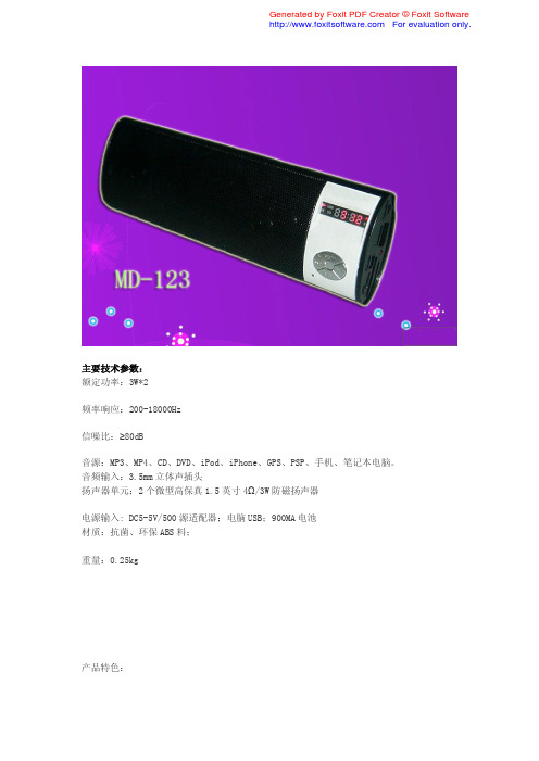
主要技术参数:额定功率:3W*2频率响应:200-18000Hz信噪比:≥80dB音源:MP3、MP4、CD、DVD、iPod、iPhone、GPS、PSP、手机、笔记本电脑。
音频输入:3.5mm立体声插头扬声器单元:2个微型高保真1.5英寸4Ω/3W防磁扬声器电源输入: DC5-5V/500源适配器;电脑USB;900MA电池材质:抗菌、环保ABS料;重量:0.25kg产品特色:1、超现代前卫造型,高档时尚2、可遥控控制(可选)、LED数码管显示、FM收音模式、高保真喇叭3、符合声学设计原理,专用声卡解码,音色柔和,层次分明,圆润甜美,通透明晰4、可连接手机,电脑,IPOD ,MP3 MP4 播放器等音频设备内置锂电池,可更换可充电可读U盘MMC SD卡使用说明:● 电池:内置锂电池,使用USB供电时,可播放音乐同时充电。
● ON/OFF:电源开关,置于ON开机,置于OFF位置关机。
● USB:移动磁盘(U盘)插槽,插入U盘可播放保存于卡上的MP3音乐。
● 充电指示灯:用于指示音箱处于在充电状态下。
● DC-5V:直流5V(0.4-1A)电源适配器,可用USB电源。
● SD/MMC:SD或者MMC卡插槽,插入SD/MMC卡可播放保存于卡上的MP3音乐。
● Line in:音频输入接口。
使用笔记本电脑,手机或者其它播放器输出连接至本机做有源音箱使用。
● MODE:模式转换键,当同时存在U盘、SD卡、FM时,此键可用于三种模式间的转换。
● V+\V-:为音量调节及歌曲选择键。
短时间按为歌曲上一首\下一首,长时间按为音量调节。
● 播放\暂停:此键用于歌曲的播放或者暂停。
● 工作指示灯:用于指示音箱处于工作状态下。
常用三极管参数

常用三极管参数一、开关晶体管型号极性 Ic Pcm VCEO VCBO (A) (W) (V) (V)D13003 NPN 1.5 40 400 700D13004 NPN 4 75 400 600D13005 NPN 4 75 400 700D13006 NPN 8 80 400 600D13007 NPN 8 80 450 700D13008 NPN 12 100 300 600D13009 NPN 12 100 400 700二、功放对管型号极性 Ptot lc VCBO(W) (A) (V)2SA1216 PNP 200 -20 -1802SC2922 NPN 200 20 1802SA1301 PNP 120 -12 -1602SC3280 NPN 120 12 1602SA1302 PNP 150 -15 -2002SC3281 NPN 150 15 2002SA1492 PNP 130 -15 -1802SC3856 NPN 130 15 2002SA1494 PNP 200 -20 -2002SC3858 NPN 200 20 2002SA1694 PNP 80 -8 -1602SC4467 NPN 80 8 1602SA1695 PNP 100 -10 -2002SC4468 NPN 100 10 2002SA1941 PNP 100 -10 -1402SC5198 NPN 100 10 1402SA1943 PNP 150 -15 -2002SC5200 NPN 150 15 2002SA1962 PNP 130 -15 -2002SC5242 NPN 130 15 2002SC1579 NPN 150 15 4002SC1580 NPN 150 15 5002SC2761 NPN 200 15 4002SD1037 NPN 100 12 1402SD1047 NPN 100 12 1602SB688 PNP 80 -10 -1202SD718 NPN 80 10 1202SB817 PNP 100 -12 -1402SD1047 NPN 100 12 1402SA1106 PNP 100 -10 -1402SC2581 NPN 100 10 2002SA1215 PNP 150 -4 -1602SC2921 NPN 150 15 160三、超声波用晶体管型号极性 Ptot lc Vceo(W) (A) (V)BUX24 NPN 350 20 400-450 BUX98A NPN 250 30 450 BUS14A NPN 250 30 450-1000BUX48A NPN 200 20 800-1200BUS13A NPN 175 15 450-1000BU508A NPN 125 8 800-1500BUV48A NPN 150 15 450-1000四、NPN硅特大功率三极管型号极性 lc Pcm Vceo Vcbo(A) (W) (V) (V)3DF50C NPN 50 500 200 2503DD5686 NPN 50 300 200 2502SC1435 NPN 40 300 600 800-12002SC2445 NPN 30 250 300/200 400/3002SC3990 NPN 35 250 800/500 900/6002SC1437 NPN 50 200 230 2302SC2921 NPN 50 200 160 2002SC2147 NPN 50 200 400 6002SC431(….6) NPN 30 200 150-300 180-500 2SC1136 NPN 30 200 200/150 200/1502SC1138 NPN 30 200 800/400 800/4002SC1139 NPN 30 200 600/300 600/3002SC1300(.02) NPN 30 200 500/250 500/250 2SC2128 NPN 30 200 200 2002SC3858 NPN 20 200 200 2502SC2507 NPN 20 200 500/400 500/4002SC2922 NPN 17 200 180 2002SC3281 NPN 15 200 200 2802SC1145 NPN 20 175 700/400 700/4002SC3455 NPN 25 160 800/500 800/5002SC5200 NPN 15 150 230 2802SC1140(..1) NPN 15 150 800/400 800/400器件型号极性 lc Pcm Vceo Vcbo(A) (W) (V) (V)2SC806A NPN 10 125 700 7002SC1142 NPN 10 125 800/400 800/4002SC2751 NPN 15 120 500 5002SC1322 NPN 15 100 250 2802SC1079 NPN 12 100 150 2002SC2304 NPN 12 100 500/400 500/4002SC1469A NPN 10 100 500/400 500/400 2SC407(..12) NPN 10 100 150-300 150-300 2SC102 NPN 7 100 200 2002SC1764 NPN 12 80 65 1502SC2303 NPN 10 100 500/400 500/4002SC1477 NPN 9 100 230 2802SC902 NPN 10 75 150 2002SC1403A NPN 8 70 180 2302SC1463 NPN 4 70 450 5502SC1051(L) NPN7 60 200 2302SC4122 NPN 7 60 1500/800 1500/8002SC768(..771) NPN 10 50 60-250 100-350 2SC758(..760) NPN 8 50 100-280 200-350 2SC270 NPN 5 50 270 3802SC862 NPN 5 50 650 700五、PNP硅特大功率三极管器件型号极性 lc(A) Pcm(W) Vceo (V)Vcbo(V) 3CD5684 PNP -50 300 -230 -2802SA1494 PNP -30 250 -200 -2502SA1109 PNP -10 200 -180 -2002SA1117 PNP -17 200 -200 -2502SA1493 PNP -15 200 -200 -2502SA1216 PNP -15 200 -180 -2002SA1215 PNP -17 200 -160 -20022SA1295 PNP -17 200 -230 -2502SA909 PNP -15 150 -200 -2502SA1043 PNP -30 150 -120 -1502SA1047 PNP -15 150 -160 -2002SA1943 PNP -15 150 -230 -2502SA1294 PNP -15 130 -230 -2502SA1003 PNP -12 120 -150 -2002SA1065 PNP -10 120 -150 -2002SA1072(…3) PNP -15 120 -160 -2002SA1187 PNP -12 120 -150 -2002SA1227(A) PNP -12 120 -160 -2002SA491 PNP -10 100 -140 -2002SA679 PNP -12 100 -120 -1502SA1695 PNP -10 100 -140 -1602SA1042 PNP -15 100 -70 -1002SA1007 PNP -10 100 -150 -1502SA1180 PNP -10 100 -180 -2002SA751 PNP -7 80 -130 -1502SA982 PNP -8 80 -140 -1602SA1672 PNP -10 80 -140 -1602SA1673 PNP -15 80 -180 -2002SA1672 PNP -8 75 -120 -1502SA745A PNP -8 70 -120 -1502SA1292 PNP -15 70 -80 -1002SA626 PNP -5 60 -80 -1002SA627 PNP -5 60 -100 -1202SA649 PNP -7 60 -150 -2002SC1513 PNP -15 60 -100 -1202SA1746 PNP -12 60 -70 -1002SA757 PNP -7 60 -120 -1502SA656(A) PNP -7 50 -130 -1502SA739 PNP -3 50 -400 -4502SA756 PNP -6 50 -100 -120六、3DD系列特大功率三极管器件型号 Pcm Icm Vceo Vcbo 塑封外型DF50C 500W 50A 200V 250V TO-3PⅢCF50C 500W -50A -200V -250V TO-3PⅢ3DD5686 300W 50A 200V 250V TO-3PⅡ 3CD5684 300W -50A -200V -250V TO-3PⅡ 3CF5 50W -5A -250V -250V TO-2203CF7 75W -7A -250V -250V TO-2203CF10 100W -10A 0-250V -250V TO-3P3CF15 150W -15A -250V -250V TO-3PⅡ3CF20 200W -20A -250V -250V TO-3PⅡ3CD6 50W -5A -300V TO-2203CD8 100W -10A -300V TO-3PⅡ3CD9 150W -15A -300V TO-3PⅡ3CD4399 200W -30A -60V -60V TO-3PⅡ 3CD5884 200W -25A -80V -80V TO-3PⅡ 3CD6609 150W 16A -140V -80V TO-3PⅡ3CD4352 125W 16A -140V -140V TO-3PⅡ3CD5880 160W 15A -80V -80V TO-3PⅡ3CD15002 200W 15A -140V -140V TO-3PⅡ3CD1618 200W 20A -160V -180V TO-3PⅡ3CD15004 250W 20A -140V -160V TO-3PⅡ3DF5 50W 5A 50-300V 80-450V TO-2203DF7 75W 7.5A 50-300V 80-450V TO-2203DF10 100W 10A 50-300V 80-450V TO-3PⅡ 3DF15 150W 15A 50-300V 80-450V TO-3PⅡ 3DF20 200W 20A 50-300V 80-450V TO-3PⅡ 3DF30 300W 30A 50-300V 80-450V TO-3PⅢ 3DF50 500W 50A 50-300V 80-450V TO-3PⅢ 3DF105 50W 3A 200-800V 300-1500V TO-220 3DD6 50W 3-5A 50-600V TO-2203DD7 75W 3.5-7.5A 50-600V TO-2203DD8 100W 5-10A 50-600V TO-3PⅡ3DD9 150W 7.5-15A 50-600V TO-3PⅡ3DD10 200W 10-20A 50-600V TO-3PⅡ3DD11 300W 15-30A 50-600V TO-3PⅡ3DD63 50W 7.5A 30-230V TO-2203DD67 75W 10A 30-230V TO-2203DD69 100W 15A 30-230V TO-3PⅡ3DD70 100W 9A 30-230V TO-3PⅡ3DD71 150W 20A 30-230V TO-3PⅡ3DD72 150W 14A 30-230V TO-3PⅡ3DD73 200W 25A 30-230V TO-3PⅡ3DD101 50W 5A 100-300V 150-350V TO-220 3DD104 50W 3A 200-800V 300-1500V TO-220 3DD162 50W 7.5A 50-400V 80-600V TO-2203DD164 75W 10A 50-400V 80-600V TO-2203DD165 100W 10A 50-400V 80-600V TO-3PⅡ3DD167 150W 15A 50-400V 80-600V TO-3PⅡ3DD168 150W 15A 50-400V 80-600V TO-3PⅡ3DD170 200W 20A 50-400V 80-600V TO-3PⅡ3DD173 250W 25A 50-400V 80-600V TO-3PⅡ3DD175 300W 30A 50-400V 80-600V TO-3PⅡ3DD259 50W 3.5A 300-800V 50-1500V TO-2203DD262 75W 5A 300-800V 50-1500V TO-2203DD265 100W 7A 300-800V 50-1500V TO-3PⅡ3DD268 150W 10A 300-800V 50-1500V TO-3PⅡ3DD271 200W 15A 300-800V 50-1500V TO-3PⅡ3DD275 300W 20A 300-800V 50-1500V TO-3PⅡ3DD4342 125W 16A 140V 140V TO-3PⅡ3DD5038 140W 20A 150V 150V TO-3PⅡ3DD3716 150W 10A 80V 100V TO-3PⅡ3DD3773 150W 16A 140V 160V TO-3PⅡ3DD5882 160W 15A 80V 80V TO-3PⅡ3DD15001 200W 15A 140V 140V TO-3PⅡ3DD5886 200W 25A 80V 80V TO-3PⅡ3DD6338 200W 25A 100V 120V TO-3PⅡ3DD5302 200W 30A 60V 60V TO-3PⅡ3DD1618 250W 20A 160V 180V TO-3PⅡ3DD15003 250W 20A 140V 160V TO-3PⅡ七、MOSFET 场效应管参数型号 PD (W) ID (A) V(BR)DSS (V) 管脚排列PIN ARRAY 封装形式IRF150 150 40 100 GDS TO-204AEIRF250 150 30 200 GDS TO-204AEIRF460 300 21 500 GDS TO-204AE IRF540 150 28 100 GDS TO-220AB IRF630 75 9 200 GDS TO-220ABIRF640 125 18 200 GDS TO-220AB IRF730 74 5.5 400 GDS TO-220ABIRF740 125 10 400 GDS TO-220AB IRF830 74 4.5 500 GDS TO-220ABIRF840 125 8 500 GDS TO-220ABIRF1404 200 162 40 GDS TO-220AB IRF1405 330 169 55 GDS TO-220AB IRF3205 200 80-110 55 GDS TO-220AB IRFP40 150 40 40 GDS TO-220AB IRFP450A 190 14 500 GDS TO-220AB IRF9640 125 -11 -200 GDS TO-220AB IRFZ44 190 50 60 GDS TO-220AB IRFZ48 45 40 55 GDS TO-220AB IRFP064 300 70 60 GDS TO-247AC IRFP150 200 40 100 GDS TO-3PIRFP250 190 30 200 GDS TO-247AC IRFP450 190 14 500 GDS TO-247AC IRFP460 280 20 500 GDS TO-247AC IRFPE40 150 5.5 800 GDS TO-247AC2N60 64 2.4 600 GDS TO-220AB3N60 75 3 600 GDS TO-220AB3N90 25 3 900 GDS TO-220AB4N60 106 4.4 600 GDS TO-220F6N60 125 6 600 GDS TO-220AB10N10 75 10 100 GDS TO-220AB10N60 180 11 600 GDS TO-220AB40N50 500 40 500 GDS TO-247AC 50N06 125 50 60 GDS TO-22060N06 150-250 60 60 GDS TO-220AB 60N100 176 60 1000 GDS TO-3PL70N06 250 70 60 GDS T0220AB75N75 300 75 75 GDS TO-3P100N10 450 100 100 GDS TO-3P。
74LS123中文资料
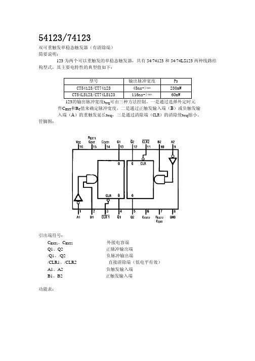
54123/74123
双可重触发单稳态触发器(有清除端)
简要说明:
123为两个可以重触发的单稳态触发器,共有54/74123和54/74LS123两种线路结构型式,其主要电特性的典型值如下:
型号 输出脉冲宽度 P D
CT54123/CT74123 45ns->∞ 230mW
CT54LS123/CT74LS123 116ns->∞ 60mW
123的输出脉冲宽度t WQ可由三种方法控制。
一是通过选择外定时元
件C EXT和R T值来确定脉冲宽度,二是通过正触发输入端(B)或负触发输
入端(A)的重触发延长t WQ,三是通过清除端(CLR)的清除使t WQ缩小。
管脚图:
引出端符号:
C EXT1、C EXT2外接电容端
Q1、Q2正脉冲输出端
/Q1、/Q2负脉冲输出端
/CLR1、/CLR2直接清除端(低电平有效)
A1、A2负触发输入端
B1、B2正触发输入端
功能表:
说明:1.外接电容接在Cext(正)和Rext/Cext(正)之间
2.为了改善脉冲宽度的精度和重复性,可在Rext/Cext和
Vcc之间接外接电阻。
3.为了得到可变脉冲宽度,可在Rext/Cext和Vcc之间接
接可变电阻。
H-高电平
L-低电平
X-任意
↑-低到高电平跳变
↓-高到低电平跳变
-一个高电平脉冲
-一个低电平脉冲
应用电路:。
VP3203ND中文资料

0.6
-4.0
-G indicates package is RoHS compliant (‘Green’). * Mil visual screening available.
Pin Configurations
DRAIN
SOURCE DRAIN
GATE
SOURCE DRAIN
Absolute Maximum Ratings
-16
V GS
= -10V
-16
V GS
= -10V
I D ( a mpe re s )
-12
I D ( a mpe re s )
-8V
-12
-8V
-8
-8
-6V
-4 -4
-6V
0
0 -5 -10 -15 -20
-4V -3V
-25 -30
-4V
0
0 -2 -4 -6
-3V
-8 -10
V DS (volts)
T he rma l R e s is ta nc e ( norma liz e d)
TO-243AA (pulsed)
TO-92 (pulsed)
0.8
TO-243AA(DC)
I D ( a mpe re s )
-1.0
TO-92 (N3)
VP2LW
W = Code for week sealed = “GreeAA (SOT-89) (N8)
● 1235 Bordeaux Drive, Sunnyvale, CA 94089 ● Tel: 408-222-8888 ●
Drain-to-source breakdown voltage Change in VGS(th) with temperature Gate body leakage Zero gate voltage drain current On-state drain current Static drain-to-source on-state resistance Change in RDS(ON) with temperature Forward transductance Input capacitance Common source output capacitance Reverse transfer capacitance Turn-on delay time Rise time Turn-off delay time Fall time Diode forward voltage drop Reverse recovery time
sdr,ddr1_2_3 ,gddr1_2_3_4_5 详细规格解释(下)
sdr,,ddr1/2/3,gddr1/2/3/4/5详细规格解释(下)sdr●GDDR4的技术特性:使用DDR3的8bit预取技术,以较低的核心频率达到更高带宽,但延迟增加;采用数据总线转位技术(DBI,Data Bus Inversion,下文做详细介绍),提高数据精度,降低功耗;地址线只有GDDR3的一半,多余线用于电源和接地,有利于提升频率,但导致延迟增加;采用多重同步码(Multi-Preamble)技术,解决了GDDR3存在的爆发限制(Burst Limitation),从连续地址读取少量数据时的性能大幅提升;电压从1.8V降至1.5V;同频功耗下降75%,2400MHz的GDDR4功耗只有2000MHz GDDR3的一半;采用136Ball FBGA封装,单颗32Bit,向下兼容GDDR3;GDDR4的确更好超,但性能提升有限由于采用了8bit预取技术,因此在相同频率下GDDR4的核心频率(即电容刷新频率)只有GDDR3的一半,理论上来讲GDDR4最高频率可达GDDR3的两倍。
但值得注意的是,虽然核心频率通过8bit预取技术减半,但GDDR4与GDDR3的I/O频率是完全相同的,因此GDDR4频率提升的瓶颈在于I/O 频率而不是核心频率。
由于制造工艺和技术水平的限制,虽然三星官方宣称早已生产出3GHz以上的GDDR4,但实际出货的GDDR4只有2GHz-2.5GHz,此后改进工艺的GDDR3也追平了这一频率。
在相同频率下,GDDR4比起GDDR3虽然功耗发热低,但延迟大性能稍弱,再加上成本高产量小,GDDR4遭受冷落并不意外。
●导致GDDR4失败的非技术方面原因GDDR3是NVIDIA和ATI参与JEDEC组织后共同制定的显存标准,而GDDR4在标准制定过程中双方产生了较大的分歧。
NVIDIA较为保守,认为应该保持DDR24bit预取技术不变,继续改进I/O控制器来提升频率;而ATI则比较激进,准备直接使用DDR38bit预取技术。
sdr,ddr1_2_3 ,gddr1_2_3_4_5 详细规格解释(上)

sdr,ddr1/2/3,gddr1/2/3/4/5详细规格解释(上)通常大家所说的DDR-400、DDR2-800、DDR3-1600等,其实并非是内存的真正频率,而是业界约定俗成的等效频率,这些DDR1/2/3内存相当于老牌SDR内存运行在400MHz、800MHz、1600MHz时的带宽,因此频率看上去很夸张,其实真正的内核频率都只有200MHz而已!内存有三种不同的频率指标,它们分别是核心频率、时钟频率和有效数据传输频率。
核心频率即为内存Cell阵列(Memory Cell Array,即内部电容)的刷新频率,它是内存的真实运行频率;时钟频率即I/O Buffer(输入/输出缓冲)的传输频率;而有效数据传输频率就是指数据传送的频率(即等效频率)。
●SDR和DDR1/2/3全系列频率对照表:通过上表就能非常直观的看出,近年来内存的频率虽然在成倍增长,可实际上真正存储单元的频率一直在133MHz-200MHz之间徘徊,这是因为电容的刷新频率受制于制造工艺而很难取得突破。
而每一代DDR的推出,都能够以较低的存储单元频率,实现更大的带宽,并且为将来频率和带宽的提升留下了一定的空间。
虽然存储单元的频率一直都没变,但内存颗粒的I/O频率却一直在增长,再加上DDR是双倍数据传输,因此内存的数据传输率可以达到核心频率的8倍之多!通过下面的示意图就能略知一二:那么,内存IO 频率为什么能达到数倍于核心频率呢?相信很多人都知道,DDR1/2/3内存最关键的技术就是分别采用了2/4/8bit 数据预取技术(Prefetch),由此得以将带宽翻倍,与此同时I/O 控制器也必须做相应的改进。
●DDR1/2/3数据预取技术原理:预取,顾名思义就是预先/提前存取数据,也就是说在I/O控制器发出请求之前,存储单元已经事先准备好了2/4/8bit数据。
简单来说这就是把并行传输的数据转换为串行数据流,我们可以把它认为是存储单元内部的Raid/多通道技术,可以说是以电容矩阵为单位的。
SOD-123型号的塑封稳压二极管商品说明书

SOD-123贴片塑封稳压二极管SOD-123 Plastic-Encapsulate Zener Diode特征Featuresz 齐纳击穿阻抗低; Low Zener Impedancez 最大功率耗散500mW; Power Dissipation of 500mW z 高稳定性和可靠性。
High Stability and High Reliability 机械数据Mechanical DataSOD-123z 封装: SOD-123封装SOD-123 Small Outline Plastic Package z 极性: 色环端为负极Polarity: Color band denotes cathode end z 环氧树脂UL 易燃等级Epoxy UL: 94V-0 z安装位置: 任意Mounting Position: Any极限值和温度特性(TA = 25℃ 除非另有规定)Maximum Ratings & Thermal Characteristics (Ratings at 25℃ ambient temperature unless otherwise specified.) 参数 Parameters符号Symbol 数值Value 单位Unit功率消耗Power DissipationPd 500 mW正向压降Forward Voltage @IF=10mA Vf 0.9 V存储温度Storage temperature rangeTs -65-+150℃ 1) Device mounted on ceramic PCB: 7.6mm x 9.4mm x 0.87mm with pad areas 25mm²2) Short duration test pulse used to minimize self-heating effect 3)f=1KHz电特性 (TA = 25℃ 除非另有规定)Electrical Characteristics (Ratings at 25℃ ambient temperature unless otherwise specified).Zener Voltage RangeMaximum Zener Impedance MaximumReverse CurrentVz@Izt IztZzt @Izt Zzk @IzkIzk IR VRTypicalTemperaturecoefficent @IZTC=mV/℃TestCurrentIZTC Device MarkingNom(V) Min(V) Max(V) mA Ω mAuA V Min Max mA BZT52B2V4 2WX 2.4 2.35 2.45 5 100 600 1.050 1.0 -3.5 0 5 BZT52B2V7 2W1 2.7 2.65 2.75 5 100 600 1.020 1.0 -3.5 0 5 BZT52B3V0 2W2 3.0 2.94 3.06 5 95 600 1.010 1.0 -3.5 0 5 BZT52B3V3 2W3 3.3 3.23 3.37 5 95 600 1.0 5 1.0 -3.5 0 5 BZT52B3V6 2W4 3.6 3.53 3.67 5 90 600 1.0 5 1.0 -3.5 0 5 BZT52B3V9 2W5 3.9 3.82 3.98 5 90 600 1.0 3 1.0 -3.5 0 5 BZT52B4V3 2W6 4.3 4.21 4.39 5 90 600 1.0 3 1.0 -3.5 05BZT52B4V7 2W7 4.7 4.61 4.79 5 80 500 1.0 3 2.0 -3.5 0.2 5 BZT52B5V1 2W8 5.1 5.00 5.20 5 60 480 1.0 2 2.0 -2.7 1.2 5 BZT52B5V6 2W9 5.6 5.49 5.71 5 40 400 1.0 1 2.0 -2.0 2.5 5 BZT52B6V2 2WA 6.2 6.08 6.32 5 10 150 1.0 3 4.0 0.4 3.7 5 BZT52B6V8 2WB 6.8 6.66 6.94 5 15 80 1.0 2 4.0 1.2 4.5 5 BZT52B7V5 2WC 7.5 7.35 7.65 5 15 80 1.0 15.0 2.5 5.3 5BZT52B8V2 2WD 8.2 8.04 8.36 5 1580 1.00.7 5.0 3.2 6.2 5 BZT52B9V1 2WE 9.1 8.929.28 5 15 100 1.00.5 6.0 3.8 7.0 5 BZT52B10 2WF 10 9.80 10.20 5 20 150 1.00.2 7.0 4.5 8.0 5 BZT52B11 2WG 11 10.78 11.22 5 20 150 1.00.1 8.0 5.4 9.0 5 BZT52B12 2WH 12 11.76 12.24 5 25 150 1.00.1 8.0 6.0 10.0 5 BZT52B13 2WI 13 12.74 13.26 5 30 170 1.00.1 8.0 7.0 11.051) 2)Zener Voltage RangeMaximum Zener Impedance MaximumReverse CurrentVz@Izt Izt Zzt @Izt Zzk @IzkIzkIR VRTypicalTemperaturecoefficent @IZTC=mV/℃TestCurrentIZTC Device MarkingNom(V) Min(V) Max(V) mA Ω mAuA V Min Max mABZT52B15 2WJ 15 14.70 15.30 5 30 200 1.00.1 10.5 9.2 13.0 5 BZT52B16 2WK 16 15.68 16.32 5 40 200 1.00.1 11.2 10.4 14.0 5 BZT52B18 2WL 18 17.64 18.36 5 45 225 1.00.1 12.6 12.4 16.0 5 BZT52B20 2WM 20 19.60 20.40 5 55 225 1.00.1 14.0 14.4 18.0 5 BZT52B22 2WN 22 21.56 22.44 5 55 250 1.00.1 15.4 16.4 20.0 5 BZT52B24 2WO 24 23.52 24.48 5 70 250 1.00.1 16.8 18.4 22.0 5 BZT52B27 2WP 27 26.46 27.54 2 80 300 0.50.1 18.9 21.4 25.3 2 BZT52B30 2WQ 30 29.40 30.60 2 80 300 0.50.1 21.0 24.4 29.4 2 BZT52B33 2WR 33 32.34 33.66 2 80 325 0.50.1 23.1 27.4 33.4 2 BZT52B36 2WS 36 35.28 36.72 2 90 350 0.50.1 25.2 30.4 37.4 2 BZT52B39 2WT 39 38.22 39.78 2 130 350 0.50.1 27.3 33.4 41.2 2 BZT52B43 2WU 43 41.16 43.84 2 100 700 1.00.1 32.0 10.0 12.0 5 BZT52B47 2WV 47 46.06 47.94 2 100 750 1.00.1 35.0 10.0 12.0 5 BZT52B51 2WW 51 49.98 52.02 2 100 750 1.00.1 38.0 10.0 12.05Breakdown characteristicsat Tj=constant (pulsed)Forward characteristicsAdmissible power dissipation versus ambient temperaturePulse thermal resistance versus pulse durationDynamic resistance versus Zener currentCapacitance versus Zener voltageDynamic resistance versus Zener current Dynamic resistance versus Zener current Thermal differential resistance versus Zener voltageDynamic resistance versus Zener voltageTemperature dependence of Zener voltage versus Zener voltageTemperature dependence of Zener voltage versus Zener voltageChange of Zener voltage versus junction temperatureChange of Zener voltage versus junction temperatureChange of Zener voltge from turn-on up to the point of thermalequilibrium versus Zener voltageSOD-123 PACKAGE OUTLINE Plastic surface mounted package焊盘设计参考Precautions: PCB DesignRecommended land dimensions for SOD-123 diode. Electrode patterns for PCBs中心距: 3.24 脚宽: 0.55 焊盘宽: 1.00 脚长: 0.50 焊盘长: 0.80 技术要求:1, 塑封体尺寸: 2.70 X 1.60 2: 未注公差为: ±0.053, 所有单位: mm。
人民电器 RDA3系列金属按钮开关 产品说明书
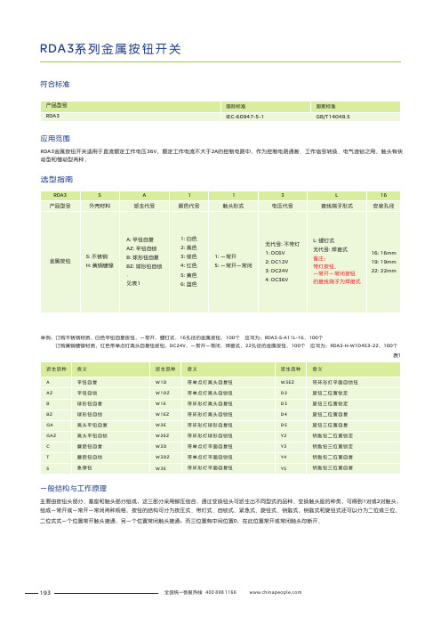
RDA3系列金属按钮开关选型指南表1举例:订购,螺钉式,16孔径的金属按钮,100个应写为:RDA3-S 100个不锈钢白色平钮自复按钮一常开黄铜镀镍红色带单点灯高头自复钮按钮一常开一常闭材质,, -A11L-16,订购材质,,DC24V ,,焊接式,22孔径的金属按钮,100个 应写为:RDA3-H-W1D453-22,100个符合标准应用范围RDA3金属按钮开关适用于直流电压36V ,额定工作电流不大于2A 的控制电路中,作为控制电路通断、工作信号转换、电气连锁之用。
触头有快动型和慢动型两种。
额定工作一般结构与工作原理主要由按钮头部分、基座和触头部分组成,这三部分采用铆压组合,通过变换钮头可派生出不同型式的品种。
变换触头座的种类,组成一常开或一常开一常闭两种规格。
按钮的结构可分为按压式、带灯式、自锁式、紧急式、旋钮式、钥匙式。
钥匙式和旋钮式还可以分为二位或三位。
二位式式一个位置常开触头接通,另一个位置常闭触头接通;而三位置有中间位置0,在此位置常开或常闭触头均断开。
可得到1对或2对触头,193外形图及尺寸平钮-选型规则螺钉式焊接式螺钉式焊接式举例:订购不锈钢,白色平钮自复按钮,一常开,螺钉式,16孔径的金属按钮 100个 应写为:RDA3-S-A11L 16 100个订购黄铜镀镍,红色平钮自锁按钮,一常闭一常闭,焊接式,22孔径的金属按钮 100个 应写为:RDA3-H-AZ4522 100个--194RDA3系列金属按钮开关外形图及尺寸球形钮-选型规则螺钉式焊接式螺钉式焊接式举例:订购不锈钢,白色球形钮自复按钮,一常开,螺钉式,16孔径的金属按钮 100个 应写为:RDA3-S-B11L 16 100个订购黄铜镀镍,红色球形钮自锁按钮,一常开一常闭,焊接式,19孔径的金属按钮 100个 应写为:RDA3-H-BZ4519 100个--195外形图及尺寸高头平钮-选型规则螺钉式焊接式螺钉式焊接式举例:订购不锈钢,白色高头平钮自复按钮,一常开,螺钉式,16孔径的金属按钮 100个 应写为:RDA3-S-GA11L16 100个订购黄铜镀镍,红色高头平钮自锁按钮,一常开一常闭,焊接式,19孔径的金属按钮 100个 应写为:RDA3-H-GAZ4519 100个--196RDA3系列金属按钮开关外形图及尺寸蘑菇钮-选型规则焊接式蘑菇钮自复、自锁举例:订购不锈钢,白色蘑菇钮自复按钮,一常开一常闭,焊接式,19孔径的金属按钮 100个 应写为:RDA3-S-C1519 100个 订购黄铜镀镍,红色蘑菇钮自锁按钮,一常开一常闭,焊接式,22孔径的金属按钮 100个 应写为:RDA3-H-T4522 100个--197外形图及尺寸急停钮-选型规则焊接式急停钮举例:订购不锈钢,红色急停钮按钮,一常开一常闭,焊接式,19孔径的金属按钮 100个 应写为:RDA3-S-S519 100个订购黄铜镀镍,红色急停钮按钮,一常开一常闭,焊接式,22孔径的金属按钮 100个 应写为:RDA3-H-S522 100个--198RDA3系列金属按钮开关外形图及尺寸带灯高钮-选型规则焊接式带单点灯带环形灯举例:订购不锈钢,白色带单点灯高头自复钮按钮,DC12V ,一常开,焊接式,16孔径的金属按钮 100个 应写为:RDA3-S-W1D11216 100个订购黄铜镀镍,红色带单点灯高头自锁钮按钮,DC24V ,一常开一常闭,焊接式,19孔径的金属按钮 100个 应写为:RDA3-H-W1DZ45319 100个--199外形图及尺寸带灯球形钮-选型规则焊接式带环形灯举例:订购不锈钢,白色带环形灯球形自复钮按钮,DC12V,一常开,焊接式,16孔径的金属按钮 100个 应写为:RDA3-S-W2E112-16 100个订购黄铜镀镍,红色带环形灯球形自复钮按钮,DC24V,一常开一常闭,焊接式,22孔径的金属按钮 100个 应写为:RDA3-H-W2EZ453-19 100个200RDA3系列金属按钮开关外形图及尺寸带灯平钮-选型规则螺钉式焊接式带环形灯带单点灯举例:订购不锈钢,白色带单点灯平面自复钮按钮,DC12V ,一常开,螺钉式,16孔径的金属按钮 100个 应写为:RDA3-S-W3D112L-16 100个订购黄铜镀镍,红色带单点灯平面自锁钮按钮,DC24V ,一常开一常闭,焊接式,22孔径的金属按钮 100个 应写为:RDA3-H-W3DZ453-22 100个201外形图及尺寸旋钮-选型规则焊接式举例:订购不锈钢,旋钮二位置锁定按钮,一常开一常闭,焊接式,19孔径的金属按钮 100个 应写为:RDA3-S-D25-19 100个订购黄铜镀镍,旋钮三位置锁定按钮,一常开一常闭,焊接式,22孔径的金属按钮 100个 应写为:RDA3-H-D35-22 100个旋钮202RDA3系列金属按钮开关外形图及尺寸钥匙钮-选型规则焊接式举例:订购不锈钢,钥匙钮二位置锁定按钮,一常开一常闭,焊接式,19孔径的金属按钮 100个 应写为:RDA3-S-Y25-19 100个 订购黄铜镀镍,钥匙钮三位置锁定按钮,一常开一常闭,焊接式,22孔径的金属按钮 100个 应写为:RDA3-H-Y35-22 100个钥匙钮203。
RD-III说明书
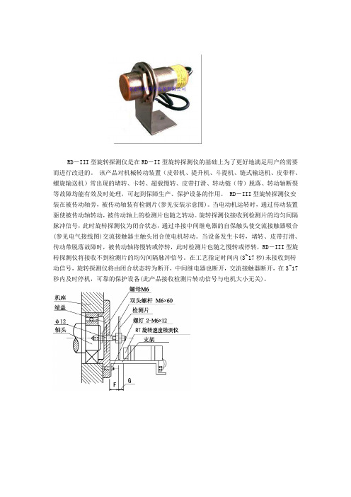
RD-III型旋转探测仪是在RD-II型旋转探测仪的基础上为了更好地满足用户的需要而进行改进的。
该产品对机械转动装置(皮带机、提升机、斗提机、链式输送机、皮带秤、螺旋输送机)常出现的堵转、卡转、超载慢转、皮带打滑、转动链(带)脱落、转动轴断裂等故障均能有效及时处理,可起到保障生产、保护设备的作用。
RD-III型旋转探测仪安装在被传动轴旁,被传动轴装有检测片(参见安装示意图)。
当电动机运转时,通过传动装置驱使被传动轴转动,被传动轴上的检测片也随之转动。
旋转探测仪接收到检测片的均匀间隔脉冲信号,此时旋转探测仪为闭合状态,通过串接中间继电器的自保触头使交流接触器吸合(参见电气接线图)交流接触器主触头闭合使电机转动。
当设备发生卡转,堵转、皮带打滑、传动带脱落故障时,被传动轴将慢转或停转,此时检测片也随之慢转或停转,RD-III型旋转探测仪将接收不到检测片的均匀间隔脉冲信号。
在工艺指定时间内(3~17秒)未接收到转动信号,旋转探测仪将由闭合状态转为断开,中间继电器也断开,交流接触器断开,在3~17秒内及时停机,可靠的保护设备(此产品接收检测片转动信号与电机大小无关)。
RI-123.3SP中文资料

ECONOLINE
DC/DC-Converter
Typical Characteristics
RI Series
RI-xx05S
Efficiency / Load
100 80 60
RI-xx3.3S
Efficiency / Load
100 80 60 40
RI-xx07S
Efficiency / Load
0% 20% 40% 60% Total Output current (%)
80%
100%
0% 20% 40% 60% Total Output current (%)
80%
100%
RI-xx12S
Efficiency / Load
100 80 60 40 100
RI-xx15S
Efficiency / Load 0515
7.55 10.20
RECOM RI-0505 ****
0.51 typ.
RECOM RI-0505 ****
4.10
0.51 typ.
1 2 3 4
Recommended Footprint Details
1.00 ø+0.15/0 2.54 0.25 2.03
Bottom View
Pin Connections Pin # 1 2 3 4 Dual -Vin +Vin –Vout +Vout
2412
80 60 40
1212 Efficiency % 0512
1215 2415
Efficiency %
20 0
20 0
0% 20% 40% 60% Total Output current (%)
E32 3MP Bullet摄像头硬件用户手册说明书
E323MP Bullet with D/N, IR, Basic WDR, Fixed lensHardware User’s Manual(PoE)Ver. 2013/01/18Table of Contents0.Precautions 31.Introduction 4Package Contents (4)Features and Benefits (5)Safety Instructions (6)Physical description (8)Basic Connections (9)Product Specification (10)2.Installation 11How to Do the Waterproof with Conduit Installation (11)How to replace pre-installed network cable with cable gland (14)3.Accessing Camera 17If you have DHCP server / router in your network: (17)If you do NOT have DHCP server / router in your network: (17)2Read these instructionsY ou should read all the safety and operating instructions before using this product.Heed all warningsY ou must adhere to all the warnings on the product and in the instruction manual. Failure to follow the safety instruction given may directly endanger people, cause damage to the system or to other equipment.ServicingDo not attempt to service this video device yourself as opening or removing covers may expose you to dangerous voltage or other hazards. Refer all servicing to qualified service personnel.TrademarksAll names used in this manual are probably registered trademarks of respective companies.LiabilityEvery reasonable care has been taken during the writing of this manual. Please inform your local office if you find any inaccuracies or omissions. We cannot be held responsible for any typographical or technical errors and reserve the right to make changes to the product and manuals without prior notice.FCC/CE RegulationNOTE: This equipment has been tested and found to comply with the limits for a Class B digital device, pursuant to Part 15 of the FCC Rules. These limits are designed to provide reasonable protection against harmful interference when the equipment is operated in a commercial environment. This equipment generates, uses, and can radiate radio frequency energy and, if not installed and used in accordance with the instruction manual, may cause harmful interference to radio communications. Operation of this equipment in a residential area is likely to cause harmful interference in which case the users will be required to correct the interference at their own expense.3Package ContentsE32 (Included camera stand/sun shield) Accessories Conduit Gland Lens Focus Tuner Warranty Card QIG 4Features and BenefitsThis is a cutting-edge digital video surveillance camera. It can compress and transmit real time images with outstanding image quality through a standard TCP/IP network. This camera is your best choice to build an intelligent IP surveillance system.H.264 High Profile/MJPEG Multi-Codec Dual StreamingThis device supports 2 compression formats, H.264 High Profile and MJPEG. It brings superior image quality at 15 frames per second up to resolution of 2048 x 1536 pixels. In Full HD 1080p (1920 x 1080), 720p (1280 x 720) and VGA resolution (640 x 480) the device reaches 30 frames per second.Built-in Hardware Motion DetectionNo more external motion sensors are required. Y ou may assign up to 3 video motion detection areas. By tuning the object size and sensitivity, it will reliably detect objects passing though is view. Hardware motion detection also offers better sensitivity and faster response time than software motion detection.Powerful Bundled Surveillance SoftwareTo extend the capabilities of the IP Camera series, a powerful surveillance program is included in the package for free. Users can easily use an existing PC as a digital video recorder. Scheduled recording and manual recording keep every important video recorded in the local hard disk. Reliable and accurate motion detection with instant warning enables immediate response in every condition. Quick and simple search and playback function lets you easily find the images and video you want.Software Development Kit SupportThis IP Camera can be integrated or controlled by applications from third party software developers. Software developers can save considerable efforts by using our Streaming Library or ActiveX control. Please contact us for details on integration support.5Safety InstructionsDon’t open the housing of the productCleaningDisconnect this video product from the power supply before cleaning.AttachmentsDo not use attachments not recommended by the video product manufacturer as they may cause hazards.Water and MoistureDo not use this video product near water, for example, near a bathtub, washbowl, kitchen sink, or laundry tub, in a wet basement, or near a swimming pool and the like.Don’t use accessories not recommended by the manufacturerOnly install this device in a dry place protected from weatherServicingDo not attempt to service this video product yourself as opening or removing covers may expose you to dangerous voltage or other hazards. Refer all servicing to qualified service personnel.Damage Requiring serviceDisconnect this video product from the power supply immediately and refer servicing to qualified service personnel under the following conditions.1) When the power-supply cord or plug is damaged2) If liquid has been spilled, or objects have fallen into the video product.3) If the video product has been directly exposed to rain or water.4) If the video product does not operate normally by following the operating Instructions inthis manual. Adjust only those controls that are covered by the instruction manual, as an improper adjustment of other controls may result in damage, and will often requireextensive work by a qualified technician to restore the video product to its normaloperation.Safety Check6Upon completion of any service or repairs to this video product, ask the service technician to perform safety checks to determine if the video product is in proper operating condition.7Physical description1) Reset ButtonStep 1: Press and continue to hold the Reset Button for 15 seconds (with a sharp tipped object, like a pen.) after the unit has successfully completed the boot process.Step 2: The Ethernet LED light will turn off for about 1~2 seconds and flash on for another second. By this time the reset to default operation is already completed. Y ou may then releasethe reset button. This length of time fluctuates slightly with the environment. The unit will come back on and stay on after a few more seconds. The unit will start up with factory defaultsettings automatically.2) Power LEDLED light will light up while the power is on. LED light will light off after the unit has successfully completed the boot process.3) Ethernet PortThe IP device connects to the Ethernet via a standard RJ45 connector. Supporting NWAY, thisIP device can auto detect the speed of local network segment (10Base-T/100Base-TX Ethernet).8Basic ConnectionsFollow the procedures below to connect the IP device to the respective apparatuses.Please use a PoE (Power over Ethernet) supported switch or injector:1) Connect your IP Camera to the PoE Switch / Injector by CA T5 or CA T6 cables with RJ45connector.2) Connect your PoE Switch / Injector to PC with another CA T5 / CA T6 network cable.910All specifications are subject to change without notice. Please check Data Sheet on our website for latest specifications.112. InstallationHow to Do the Waterproof with Conduit InstallationBeside the bundled network cable, you also can use conduit and follow the installation procedure to make the camera be water-resistant even for the situations where the camera can easily be flooded by pouring rain.The important part to focus on during the installation: The protection of the cabling has to be done by a proper flex conduit. The size of the flex conduit that matches with the conduit gland is 1/2”. Please note that the conduit gland is included to the package of the bullet camera.The following images show the step-by-step procedure of completing the water-proof installation.Disassemble the conduit gland as shown on the photo. 1.Pull the network cable through the flex conduit.Please note that the size of the conduit and the gland is big enough to let the RJ-45 connector pass through all the way. 2.Two pieces from the conduit gland set will beattached to flex conduit first.123.Remove the bundled network cable andconnector from back side cover of the camera. 4.The third piece of conduit gland goes throughthe back side cover of the camera. 5.The fourth piece (locking nut) is used to lockthe gland firmly from the inside of the back side cover. 6.Pull the network cable through the back sidecover of the camera. 7.Connect the flex conduit to the back side coverof the camera.138. Tighten the domed sealing nut.9.Plug the network cable into the camera ’s RJ-45 connector before closing the back side of the camera. If you are not using PoE and need an additional power cord then please connect it at this stage, too.10. Tighten the screws of the back side of the camera properly.11. Finally, the bullet camera with properly mounted flex conduit as well as with proper outdoor bracket would look like this. The camera is now ready to withstand even the most severe rain storms.14How to replace pre-installed network cable with cable glandThe camera bundled cable gland with pre-installed network cable is M20 X 1.5 Matric thread. It is resistant to salt water, weak acid, alcohol, oil, grease and common solvency.The cable gland consists of five parts: Lock Nut, Body, Seal, Claw and Sealing Nut as shown below.The cable gland can hold cable firmly and have a wide range of network cable sizes, you can change suitable network cable quickly and easily to fulfil the installation environment. It is not necessary to dismantle the cable gland any further than illustrated below.The naked length of pre-installed network cable is around 14 cm.14 cmSealing NutClawSeal15The following images show the step-by-step procedure of replacing network cable and completing the water-proof installation.1.Open the back side cover from camera, and remove the network cable, and loosen the sealing nut to release the network cable from camera.2.Separate the seal from the claw.3.Squeeze the seal and then pull out the bundled network cable.4.Pull the new network cable through Sealing Nut, Claw, Seal and cable gland on the back side cover of camera sequentially.12165.Assemble the Seal and Claw, and then Insert thenetwork cable to RJ-45 PoE connector.6. Tighten the screws of the back side cover on the camera properly7.Tighten the sealing nut as far as possible.8.Finally, the bullet camera is now properly mounted with waterproof cabling and is ready to attach to the proper outdoor bracket.213.Accessing CameraIf you have DHCP server / router in your network:Many network server / routers are able to automatically provide IP addresses through DHCP. If you are using such a network, just plug in your computer and IP Camera into the network and your IP device will acquire network address by itself. Find and access the device with our IP Utility program. Y ou may download it at:/UtilityIf you do NOT have DHCP server / router in your network:1. Configure your PC to use the same subnet by changing your PC’s IP address to thesubnet with prefix 192.168.0.XXX. The last number should be anything from 1 to 254except 100 and other occupied IP addresses. Subnet mask should be 255.555.255.0.2. The default IP used by this device is 192.168.0.100. Please make sure your PC isNOT using this address and that no two equipments use the same IP address in the network.3. Change your IP address by going to Control Panel ->Manage Network Connections ->Right click on the connection to change -> Option -> TCP/IP IPv4 Properties.174. Open Internet Explorer (Version 6.0 or above) , and type in the Default IP:192.168.0.1005. When you see the login window, please input default user and password:Default User: Admin Password: 123456Please set the settings as below.●IP address: 192.168. 0.xxx●Subnet mask: 255.255.255. 0(NOTE: xxx should be a numberfrom 1 to 254 except 100, which isused by the IP device. Please alsomake sure that no two equipmentsuse the same IP address in thesame network.) 18196. After logging in, you will see the video from camera. To go to the main menu, click the“Setup” button on the top left.If you are using a single camera, this is enough to access the device.If you are using multiple devices, you need to change the current device to another unused IP address, so that when the next device is connected to the network, no two devices use the same IP . Please perform the following steps.7. Go to IP Settings -> Connection Type8. Change the IP mode to Static.9. Change the IP to 192.168.0.101 or any other unused IPs. Do NOT use the PC ’s IPaddress or 192.168.0.100.). If this is not the first device you add to the network, please also avoid other devices ’IPs.2010. Click “Apply ”11. Please go to System -> Save & Reboot, and click “Apply ”. Internet Explorer will closeafter a few seconds. This is normal.12. Wait for 30 seconds, and open IE again to connect to the new IP . (In this example,192.168.0.101). For the second device or more you add into the network, please type the correct IP .13. Adjust the default Video setting by going to Video -> VideoPlease refer the firmware manual for the detail information.。
D213中文资料
18.0 VDC
30.0
48 VDC Input -0.7
55.0
Lead Temperature
1.5 mm From Case For 10 Sec
260
ºC
Internal Power Dissipation
All Models
650
mW
Caution: Exceeding Absolute Maximum Ratings may damage the module. These are not continuous operating ratings.
Conditions
Min. Typ. Max. ±1.0 ±3.0
Units %
Output Voltage Balance
Dual Output , Balanced Loads
±1.0
%
Line Regulation
For Vin Change of 1%
±1.2
%
Load Regulation
Case
+100
ºC
Storage Temperature Range
-40
+125
ºC
Cooling
Free Air Convection
Humidity
RH, Non-condensing
95
%
Physical
MicroPower Direct
232 Tosca Drive Stoughton, MA 02072 USA
25
24 21.6 - 26.4 92
10
24 21.6 - 26.4 108
10
24 21.6 - 26.4 101
东芝DTC123EP D补偿电阻晶体管使用说明书

MUN5331DW1,NSBC123EPDXV6 Complementary Bias Resistor TransistorsR1 = 2.2 k W, R2 = 2.2 k WNPN and PNP Transistors with Monolithic Bias Resistor NetworkThis series of digital transistors is designed to replace a single device and its external resistor bias network. The Bias Resistor Transistor (BRT) contains a single transistor with a monolithic bias network consisting of two resistors; a series base resistor and a base-emitter resistor. The BRT eliminates these individual components by integrating them into a single device. The use of a BRT can reduce both system cost and board space.Features•Simplifies Circuit Design•Reduces Board Space•Reduces Component Count•S and NSV Prefix for Automotive and Other Applications Requiring Unique Site and Control Change Requirements;AEC-Q101 Qualified and PPAP Capable*•These Devices are Pb-Free, Halogen Free/BFR Free and are RoHS CompliantMAXIMUM RATINGS(T A = 25°C both polarities Q1(PNP) & Q2 (NPN), unless otherwise noted) Rating Symbol Max Unit Collector-Base Voltage V CBO50Vdc Collector-Emitter Voltage V CEO50Vdc Collector Current − Continuous I C100mAdc Input Forward Voltage V IN(fwd)12Vdc Input Reverse Voltage V IN(rev)10Vdc Stresses exceeding those listed in the Maximum Ratings table may damage the device. If any of these limits are exceeded, device functionality should not be assumed, damage may occur and reliability may be affected.ORDERING INFORMATIONDevice Package Shipping†MUN5331DW1T1G SOT−3633,000 / Tape & Reel NSVMUN5331DW1T1G*SOT−3633,000 / Tape & Reel NSBC123EPDXV6T1G SOT−5634,000 / Tape & Reel †For information on tape and reel specifications, including part orientation and tape sizes, please refer to our Tape and Reel Packaging Specifications Brochure, BRD8011/D.MARKING DIAGRAMSPIN CONNECTIONS31M GG1631 M GG131=Specific Device CodeM=Date Code*G=Pb-Free Package (Note: Microdot may be in either location) *Date Code orientation may vary depending up-on manufacturing location.SOT−363CASE 419BSOT−563CASE 463A(1)(2)(3)(6)(5)(4)THERMAL CHARACTERISTICSCharacteristic Symbol Max Unit MUN5331DW1 (SOT−363) ONE JUNCTION HEATEDTotal Device DissipationT A = 25°C(Note1)(Note2) Derate above 25°C(Note1)(Note2)P D1872561.52.0mWmW/°CThermal Resistance,(Note1) Junction to Ambient(Note2)R q JA670490°C/WMUN5331DW1 (SOT−363) BOTH JUNCTION HEATED (Note3)Total Device DissipationT A = 25°C(Note1)(Note2) Derate above 25°C(Note1)(Note2)P D2503852.03.0mWmW/°CThermal Resistance,Junction to Ambient(Note1)(Note2)R q JA493325°C/WThermal Resistance,Junction to Lead(Note1)(Note2)R q JL188208°C/WJunction and Storage Temperature Range T J, T stg−55 to +150°C NSBC123EPDXV6 (SOT−563) ONE JUNCTION HEATEDTotal Device DissipationT A = 25°C(Note1) Derate above 25°C(Note1)P D3572.9mWmW/°CThermal Resistance,Junction to Ambient(Note1)R q JA350°C/WNSBC123EPDXV6 (SOT−563) BOTH JUNCTION HEATED (Note3)Total Device DissipationT A = 25°C(Note1) Derate above 25°C(Note1)P D5004.0mWmW/°CThermal Resistance,Junction to Ambient(Note1)R q JA250°C/WJunction and Storage Temperature Range T J, T stg−55 to +150°C1.FR−4 @ Minimum Pad.2.FR−*****×1.0 Inch Pad.3.Both junction heated values assume total power is sum of two equally powered channels.ELECTRICAL CHARACTERISTICS (T A=25°C both polarities Q1 (PNP) & Q2 (NPN), unless otherwise noted)Characteristic Symbol Min Typ Max Unit OFF CHARACTERISTICSCollector-Base Cutoff Current (V CB=50V, I E=0)I CBO−−100nAdcCollector-Emitter Cutoff Current (V CE=50V, I B=0)I CEO−−500nAdcEmitter-Base Cutoff Current (V EB=6.0V, I C=0)I EBO−− 2.3mAdcCollector-Base Breakdown Voltage (I C=10m A, I E=0)V(BR)CBO50−−VdcCollector-Emitter Breakdown Voltage (Note4) (I C=2.0mA, I B=0)V(BR)CEO50−−VdcON CHARACTERISTICSDC Current Gain (Note4) (I C=5.0mA, V CE=10V)h FE8.015−Collector-Emitter Saturation Voltage (Note4) (I C=10mA, I B=5.0mA)V CE(sat)−−0.25VInput Voltage (Off)(V CE=5.0V, I C=1.0mA) (NPN) (V CE=5.0V, I C=1.0mA) (PNP)V i(off)−−1.31.2−−VdcInput Voltage (On)(V CE=0.2V, I C=20mA) (NPN)(V CE=0.2V, I C=20mA) (PNP)V i(on)−−1.81.9−−VdcOutput Voltage (On)(V CC=5.0V, V B=2.5V, R L=1.0k W)V OL−−0.2VdcOutput Voltage (Off)(V CC=5.0V, V B=0.25V, R L=1.0k W)V OH4.9−−VdcInput Resistor R1 1.5 2.2 2.9k W Resistor Ratio R1/R20.8 1.0 1.2Product parametric performance is indicated in the Electrical Characteristics for the listed test conditions, unless otherwise noted. Product performance may not be indicated by the Electrical Characteristics if operated under different conditions.4.Pulsed Condition: Pulse Width=300ms, Duty Cycle ≤2%.Figure 1. Derating CurveAMBIENT TEMPERATURE (°C)50100150200250300PD,POWERDISSIPATION(mW)(1) SOT−363; 1.0×1.0 Inch Pad(2) SOT−563; Minimum Pad350400Figure 2. V CE(sat) vs. I CFigure 3. DC Current GainI C , COLLECTOR CURRENT (mA)I C , COLLECTOR CURRENT (mA)Figure 4. Output CapacitanceFigure 5. Output Current vs. Input VoltageV R , REVERSE VOLTAGE (V)V in , INPUT VOLTAGE (V)0.1110100Figure 6. Input Voltage vs. Output CurrentI C , COLLECTOR CURRENT (mA)V C E (s a t ), C O L L E C T O R −E M I T T E R V O L T A G E (V )h F E , D C C U R R E N T G A I NC o b , O U T P U T C A P A C I T A N C E (p F )I C , C O L L E C T O R C U R R E N T (m A )V i n , I N P U T V O L T A G E (V )Figure 7. V CE(sat) vs. I CFigure 8. DC Current GainI C , COLLECTOR CURRENT (mA)I C , COLLECTOR CURRENT (mA)0.010.11Figure 9. Output CapacitanceFigure 10. Output Current vs. Input VoltageV R , REVERSE VOLTAGE (V)V in , INPUT VOLTAGE (V)Figure 11. Input Voltage vs. Output CurrentI C , COLLECTOR CURRENT (mA)V C E (s a t ), C O L L E C T O R −E M I T T E R V O L T A G E (V )h F E , D C C U R R E N T G A I NC o b , O U T P U T C A P A C I T A N C E (p F )I C , C O L L E C T O R C U R R E N T (m A )V i n , I N P U T V O L T A G E (V )SC −88/SC70−6/SOT −363CASE 419B −02ISSUE YDATE 11 DEC 2012SCALE 2:1NOTES:1.DIMENSIONING AND TOLERANCING PER ASME Y14.5M, 1994.2.CONTROLLING DIMENSION: MILLIMETERS.3.DIMENSIONS D AND E1 DO NOT INCLUDE MOLD FLASH,PROTRUSIONS, OR GATE BURRS. MOLD FLASH, PROTRU-SIONS, OR GATE BURRS SHALL NOT EXCEED 0.20 PER END.4.DIMENSIONS D AND E1 AT THE OUTERMOST EXTREMES OF THE PLASTIC BODY AND DATUM H.5.DATUMS A AND B ARE DETERMINED AT DATUM H.6.DIMENSIONS b AND c APPLY TO THE FLAT SECTION OF THE LEAD BETWEEN 0.08 AND 0.15 FROM THE TIP .7.DIMENSION b DOES NOT INCLUDE DAMBAR PROTRUSION.ALLOWABLE DAMBAR PROTRUSION SHALL BE 0.08 TOTAL IN EXCESS OF DIMENSION b AT MAXIMUM MATERIAL CONDI-TION. THE DAMBAR CANNOT BE LOCATED ON THE LOWER RADIUS OF THE FOOT.XXXM G G XXX = Specific Device Code M = Date Code*G = Pb −Free Package GENERICMARKING DIAGRAM*16STYLES ON PAGE 2DIM MIN NOM MAX MILLIMETERS A −−−−−− 1.10A10.00−−−0.10dddb 0.150.200.25C 0.080.150.22D 1.80 2.00 2.20−−−−−−0.0430.000−−−0.0040.0060.0080.0100.0030.0060.0090.0700.0780.086MIN NOM MAX INCHES0.100.004E1 1.15 1.25 1.35e 0.65 BSC L 0.260.360.462.00 2.10 2.200.0450.0490.0530.026 BSC0.0100.0140.0180.0780.0820.086(Note: Microdot may be in either location)*Date Code orientation and/or position may vary depending upon manufacturing location.*For additional information on our Pb −Free strategy and soldering details, please download the ON Semiconductor Soldering and Mounting Techniques Reference Manual, SOLDERRM/D.SOLDERING FOOTPRINT*DIMENSIONS: MILLIMETERS0.306XRECOMMENDEDSIDE VIEWEND VIEWPLANEDETAIL AE A20.700.90 1.000.0270.0350.039L20.15 BSC 0.006 BSC aaa 0.150.006bbb 0.300.012ccc 0.100.0046X*This information is generic. Please refer to device data sheet for actual part marking.Pb −Free indicator, “G” or microdot “G ”, may or may not be present. Some products may not follow the Generic Marking.MECHANICAL CASE OUTLINEPACKAGE DIMENSIONSON Semiconductor and are trademarks of Semiconductor Components Industries, LLC dba ON Semiconductor or its subsidiaries in the United States and/or other countries.ON Semiconductor reserves the right to make changes without further notice to any products herein. ON Semiconductor makes no warranty, representation or guarantee regarding the suitability of its products for any particular purpose, nor does ON Semiconductor assume any liability arising out of the application or use of any product or circuit, and specifically disclaims any and all liability, including without limitation special, consequential or incidental damages. ON Semiconductor does not convey any license under its patent rights nor theSTYLE 1:PIN 1.EMITTER 22.BASE 23.COLLECTOR 14.EMITTER 15.BASE 16.COLLECTOR 2STYLE 3:CANCELLEDSTYLE 2:CANCELLEDSTYLE 4:PIN 1.CATHODE2.CATHODE3.COLLECTOR4.EMITTER5.BASE6.ANODESTYLE 5:PIN 1.ANODE2.ANODE3.COLLECTOR4.EMITTER5.BASE6.CATHODESTYLE 6:PIN 1.ANODE 22.N/C3.CATHODE 14.ANODE 15.N/C6.CATHODE 2STYLE 7:PIN 1.SOURCE 22.DRAIN 23.GATE 14.SOURCE 15.DRAIN 16.GATE 2STYLE 8:CANCELLEDSTYLE 11:PIN 1.CATHODE 22.CATHODE 23.ANODE 14.CATHODE 15.CATHODE 16.ANODE 2STYLE 9:PIN 1.EMITTER 22.EMITTER 13.COLLECTOR 14.BASE 15.BASE 26.COLLECTOR 2STYLE 10:PIN 1.SOURCE 22.SOURCE 13.GATE 14.DRAIN 15.DRAIN 26.GATE 2STYLE 12:PIN 1.ANODE 22.ANODE 23.CATHODE 14.ANODE 15.ANODE 16.CATHODE 2STYLE 13:PIN 1.ANODE2.N/C3.COLLECTOR4.EMITTER5.BASE6.CATHODE STYLE 14:PIN 1.VREF2.GND3.GND4.IOUT5.VEN6.VCCSTYLE 15:PIN 1.ANODE 12.ANODE 23.ANODE 34.CATHODE 35.CATHODE 26.CATHODE 1STYLE 17:PIN 1.BASE 12.EMITTER 13.COLLECTOR 24.BASE 25.EMITTER 26.COLLECTOR 1STYLE 16:PIN 1.BASE 12.EMITTER 23.COLLECTOR 24.BASE 25.EMITTER 16.COLLECTOR 1STYLE 18:PIN 1.VIN12.VCC3.VOUT24.VIN25.GND6.VOUT1STYLE 19: PIN 1.I OUT2.GND3.GND4.V CC5.V EN6.V REF STYLE 20:PIN 1.COLLECTOR2.COLLECTOR3.BASE4.EMITTER5.COLLECTOR6.COLLECTORSTYLE 22:PIN 1.D1 (i)2.GND3.D2 (i)4.D2 (c)5.VBUS6.D1 (c)STYLE 21:PIN 1.ANODE 12.N/C3.ANODE 24.CATHODE 25.N/C6.CATHODE 1STYLE 23:PIN 1. Vn2.CH13.Vp4.N/C5.CH26.N/CSTYLE 24:PIN 1.CATHODE2.ANODE3.CATHODE4.CATHODE5.CATHODE6.CATHODESTYLE 25:PIN 1.BASE 12.CATHODE3.COLLECTOR 24.BASE 25.EMITTER6.COLLECTOR 1STYLE 26:PIN 1.SOURCE 12.GATE 13.DRAIN 24.SOURCE 25.GATE 26.DRAIN 1STYLE 27:PIN 1.BASE 22.BASE 13.COLLECTOR 14.EMITTER 15.EMITTER 26.COLLECTOR 2STYLE 28:PIN 1.DRAIN2.DRAIN3.GATE4.SOURCE5.DRAIN6.DRAINSTYLE 29:PIN 1.ANODE2.ANODE3.COLLECTOR4.EMITTER5.BASE/ANODE6.CATHODESC−88/SC70−6/SOT−363CASE 419B−02ISSUE YDATE 11 DEC 2012STYLE 30:PIN 1.SOURCE 12.DRAIN 23.DRAIN 24.SOURCE 25.GATE 16.DRAIN 1Note: Please refer to datasheet forstyle callout. If style type is not calledout in the datasheet refer to the devicedatasheet pinout or pin assignment.SOT −563, 6 LEADCASE 463A ISSUE HDATE 26 JAN 2021SCALE 4:16MECHANICAL CASE OUTLINEPACKAGE DIMENSIONSSOT −563, 6 LEADCASE 463A ISSUE HDATE 26 JAN 2021XX = Specific Device Code M = Month Code G = Pb −Free PackageXX MG GENERICMARKING DIAGRAM*1*This information is generic. Please refer todevice data sheet for actual part marking.Pb −Free indicator, “G” or microdot “G ”, may or may not be present. Some products maynot follow the Generic Marking.ON Semiconductor and are trademarks of Semiconductor Components Industries, LLC dba ON Semiconductor or its subsidiaries in the United States and/or other countries.ON Semiconductor reserves the right to make changes without further notice to any products herein. ON Semiconductor makes no warranty, representation or guarantee regarding the suitability of its products for any particular purpose, nor does ON Semiconductor assume any liability arising out of the application or use of any product or circuit, and specifically disclaims any and all liability, including without limitation special, consequential or incidental damages. ON Semiconductor does not convey any license under its patent rights nor thePUBLICATION ORDERING INFORMATIONTECHNICAL SUPPORTLITERATURE FULFILLMENT:。
EMD12324P资料

512M: 16M x 32 Mobile DDR SDRAM Document Title512M: 16M x 32 Mobile DDR SDRAMRevision HistoryRevision No. Date History0.0Aug 21, 2007 Initial DraftEmerging Memory & Logic Solutions Inc.4F Korea Construction Financial Cooperation B/D, 301-1 Yeon-Dong, Jeju-Do, Korea Zip Code : 690-717 Tel : +82-64-740-1700 Fax : +82-64-740-1750 / Homepage : The attached datasheets provided by EMLSI reserve the right to change the specifications and products. EMLSI will answer to your questions about device. If you have any questions, please contact the EMLSI office.512M: 16M x 32 Mobile DDR SDRAM512M : 16M x 32bit Mobile DDR SDRAMTable 1: ORDERING INFORMATIONNOTE :1. EMLSI is not designed or manufactured for use in a device or system that is used under circumstance in which human life is potentially at stake. Please contact to the memory marketing team in EMLSI when considering the use of a product contained herein for any specific purpose, such as medical, aerospace, nuclear, military, vehicular or undersea repeater use.Part No.Max Freq.InterfacePackage RemarkEMD12324P-60(DDR332)166(CL3), 111(CL2)LVCMOSWafer Biz.EMD12324P-75(DDR266)133(CL3), 83(CL2)FEATURES1.8V power supply, 1.8V I/O powerLVCMOS compatible with multiplexed address.Double-data-rate architecture; two data transfers per clock cycleBidirectional data strobe(DQS) Four banks operation.MRS cycle with address key programs. CAS latency (2, & 3). Burst length (2, 4, & 8).Burst type (Sequential & Interleave). Differential clock inputs(CK and CKB). EMRS cycle with address key programs. PASR(Partial Array Self Refresh). DS (Driver Strength) Internal auto TCSR(Temperature Compensated Self Refresh) Deep power-down(DPD) mode. DM for write masking only.Auto refresh and self refresh modes. 64 refresh period (8K cycle).Operating temperature range (-25 ~ 85).GENERAL DESCRIPTIONThis EMD12324P is 536,870,912 bits synchronous double data rate Dynamic RAM. Each 134,217,728 bits bank is organized as 8,192 rows by 512columns by 32 bits, fabricated with EMLSI’s high performance CMOS technology.This device uses a double data rate architecture to achieve high-speed operation. The double data rate architecture is essentially a 2n-prefetch architecture with an interface designed to transfer two data words per clock cycle at the I/O balls.Range of operating frequencies, programmable burst lengths and programmable latencies allow the same device to be useful for a variety of high bandwidth and high performance memory system applications.512M: 16M x 32 Mobile DDR SDRAMTable 2: Pad DescriptionSymbol Type DescriptionsCK, CKB Input Clock : CK and CKB are differential clock inputs. All address and control input signals are sampled on the crossing of the positive edge of CK and negative edge of CKB. Input and output data is referenced to the crossing of CK and CKB(both directions of crossing). Internal clock signals are derived from CK/ CKB.CKE Input Clock Enable : CKE HIGH activates, and CKE LOW deactivates internal clock signals, and device input buffers and output drivers. Taking CKE LOW provides PRECHARGE POWER-DOWN and SELF REFRESH operation(all banks idle), or ACTIVE POWER-DOWN(row ACTIVE in any bank). CKE is synchronous for all functions except for SELF REFRESH EXIT, which is achieved asynchronously. Input buffers, excluding CK, CKB and CKE, are disabled during power-down and self refresh mode which are contrived for low standby power consumption.CSB Input Chip Select : CSB enables (registered LOW) and disables (registered HIGH) the command decoder. All commands are masked when CSB is registered HIGH. CSB provides for external bank selection on systems with multiple banks. CSB is considered part of the command code.RASB, CASB,WEBInput Command Inputs: CASB, RASB, and WEB(along with CSB) define the command being entered.DM0~DM3 Input Input Data Mask: DM is an input mask signal for write data. Input data is masked when DM is sampled. HIGH along with that input data during a WRITE access. DM is sampled on both edges of DQS. Data Mask pins include dummy loading internally, to match the DQ and DQS loading.BA0, BA1 Input Bank Address Inputs: BA0 and BA1 define to which bank an ACTIVE, READ, WRITE or PRECHARGE command is being applied.A0 ~ A12 Input Address Inputs: provide the row address for ACTIVE commands, and the column address and AUTO PRECHARGE bit for READ / WRITE commands, to select one location out of the memory array in the respective bank. The address inputs also provide the op-code during a MODE REGISTER SET com-mand.DQ0~DQ31 I/O Data Bus: Input / OutputDQS0~DQS3 I/O Data Strobe: Output with read data, input with write data. Edge-aligned with read data, center-aligned with write data. Used to capture write data. For x32 device, DQS0 corresponds to the data on DQ0-DQ7, DQS1 corresponds to the data on DQ8-DQ15, DQS2 corresponds to the data on DQ16-DQ23, and DQS3 corresponds to the data on DQ24-DQ31VDD Supply Power Supply512M: 16M x 32 Mobile DDR SDRAMDevice OperationSimplified State DiagramPower OnDeep Power DownPrecharge All BanksIdle All banks prechargedSelf RefreshMRS EMRSAuto RefreshPrecharge Power DownActive Power DownRow ActiveBurst StopWRITE WRITE APrecharge PREALLREAD AREADPower appliedDPDSXMRSDPDSACTREFABSTREADREADAWRITEAPRE REFSXREFSCKEL CKEHCKELCKEH WRITEREADREADA READAPREPREPREWRITEAAutomatic Sequence Command SequenceACT = ActiveBST = Burst Terminate CKEL = Enter Power-Down CKEH =Exit Power-Down DPDS = Enter Deep Power-Down DPDSX = Exit Deep Power-DownEMRS = Ext. Mode Reg. Set MRS = Mode Register Set PRE = PrechargePREALL = Precharge All Banks REFA = Auto Refresh REFS = Enter Self RefreshREFSX = Exit Self Refresh READ = Read w/o Auto Precharge READA = Read with Auto Precharge WRITE = Write w/o Auto Precharge WRITEA = Write with Auto PrechargeREADWRITE512M: 16M x 32 Mobile DDR SDRAM FUNCTIONAL BLOCK DIAGRAM512M: 16M x 32 Mobile DDR SDRAMElectrical SpecificationsTable 3: ABSOLUTE MAXIMUM RATINGSNOTE :Permanent device damage may occur if ABSOLUTE MAXIMUM RATINGS are exceeded.Functional operation should be restricted to recommended operating condition.Exposure to higher than recommended voltage for extended periods of time could affect device reliability.Table 4: DC OPERATING CONDITIONSRecommended operating conditions (Voltage referenced to V SS = 0V, T A = -25o C~ 85o C for Extended)1. Under all conditions, VDDQ must be less than or equal to VDD.2. These parameters should be tested at the pin on actual components and may be checked at either the pin or the pad in simulation.Table 5: CAPACITANCE (V DD = 1.8V, V DDQ = 1.8V, T A = 25, f=1)ParameterSymbol Value Unit Voltage on any pin relative to V SSV IN ,V OUT -0.5 ~ 2.5V Voltage on V DD and V DDQ supply relative to V SS V DD , V DDQ-0.5 ~ 2.5VStorage temperature T STG -55 ~ +150Power dissipation P D 1.0WShort circuit current I OS50ParameterSymbol Min Typ Max Unit Note Supply voltage V DD 1.7 1.8 1.95V 1V DDQ 1.7 1.8 1.95V 1Input logic high voltage V IH 0.8 x V DDQ1.8V DDQ + 0.3V 2Input logic low voltage V IL -0.300.3V 2Output logic high voltage V OH 0.9 x V DDQ--V I OH = -0.1Output logic low voltage V OL --0.1 x V DDQVI OL = 0.1Input leakage current I LI -2-2Output leakage current I LO-5-5PinSymbol Min Max Unit NoteInput capacitance(ADD, BA0~1, RASB, CASB, WEB, CSB, CKE)C IN1 1.5 3.0Input capacitance(CK, CKB)C IN2 1.5 3.5Data & DQS input/output capacitance C out 2.0 4.5Input capacitance(DM)C IN32.04.5512M: 16M x 32 Mobile DDR SDRAM Table 6: DC CHARACTERISTICSRecommended operating conditions (Voltage referenced to VSS = 0V, T A = -25 to 85)Parameter Symbol Test ConditionVersionUnit -60-75Operating one bank active-precharge current I DD0t RC = t RCmin; t CK = t CKmin; CKE is HIGH; CSB is HIGHbetween valid commands; address inputs are SWITCH-ING; data bus inputs are STABLE10080mAPrecharge power-down standby current I DD2Pall banks idle, CKE is LOW; CSB is HIGH, t CK = t CKmin;address and control inputs are SWITCHING; data businputs are STABLE0.6mAPrecharge power-down standby current with clock stop I DD2PSall banks idle, CKE is LOW; CSB is HIGH, CK = LOW,CKB = HIGH; address and control inputs are SWITCHING;data bus inputs are STABLE0.6Precharge non power-down standby current I DD2Nall banks idle, CKE is HIGH; CSB is HIGH, t CK = t CKmin;address and control inputs are SWITCHING; data businputs are STABLE2520mAPrecharge non power-down standby current with clock stop I DD2NSall banks idle, CKE is HIGH; CSB is HIGH, CK = LOW,CKB = HIGH; address and control inputs are SWITCHING;data bus inputs are STABLE55Active power-down standby current I DD3Pone bank active, CKE is LOW; CSB is HIGH, t CK =t CKmin; address and control inputs are SWITCHING; databus inputs are STABLE8mAActive power-down standby current with clock stop I DD3PSone bank active, CKE is LOW; CSB is HIGH, CK = LOW,CKB = HIGH; address and control inputs are SWITCHING;data bus inputs are STABLE5Active non power-down standby current I DD3None bank active, CKE is HIGH; CSB is HIGH, t CK =t CKmin; address and control inputs are SWITCHING; databus inputs are STABLE2525mAActive non power-down standby current with clock stop I DD3NSone bank active, CKE is HIGH; CSB is HIGH, CK = LOW,CKB = HIGH; address and control inputs are SWITCHING;data bus inputs are STABLE1010mAOperating burst read current I DD4Rone bank active; BL=4; CL=3; t CK = t CKmin; continuousread bursts; Iout = 0 mA; address inputs are SWITCHING;50% data change each burst transfer160130mAOperating burst write current I DD4Wone bank active; t CK = t CKmin; continuous write bursts;address inputs are SWITCHING; 50% data change eachburst transfer130105mAAuto-Refresh current I DD5t RC = t RFCmin; burst refresh; CKE is HIGH;address and control inputs are SWITCHING; data businputs are STABLE120120mASelf Refresh Current I DD6CKE is LOW, CK = LOW, CKB= HIGH; Extended Mode Reg-ister set to all 0s; address andcontrol inputs are STABLE;data bus inputs are STABLETCSR Range45*185°CFull Array350600µA1/2 of Full Array2505001/4 of Full Array200450Deep Power-Down Current I DD8Address and Control inputs are STABLE;data bus inputs are STABLE1010µA512M: 16M x 32 Mobile DDR SDRAMNOTE :1. IDD specifications are tested after the device is properly initialized2. Input slew rate is 1V/ns.3. Definitions for IDD:LOW is defined as V IN 0.1 * VDDQ ; HIGH is defined as V IN 0.9 * VDDQ ;STABLE is defined as inputs stable at a HIGH or LOW level ; SWITCHING is defined as :- address and command : inputs changing between HIGH and LOW once per two clock cycles ;- data bus inputs : DQ changing between HIGH and LOW once per clock cycle ; DM and DQS are STABLETable 7: AC OPERATING TEST CONDITIONS(V DD = 1.7V ~ 1.95V, T A = -25~85for Extended)NOTE :1. Under all conditions, VDDQ must be less than or equal to VDD.2. These parameters should be tested at the pin on actual components and may be checked at either the pin or the pad in simulation.3. CK and CKB crossing voltage.ParameterValueUnitNoteAC input levels(Vih/Vil)0.8V DDQ / 0.2 V DDQV Input timing measurement reference level 0.5V DDQ V Input rise and fall time1.0V /Output timing measurement reference level 0.5V DDQVVix0.4V DDQ (Min) / 0.6V DDQ (Max)V3Output load condition See Figure 21.8V 13.9V OH (DC) = 0.9V DDQ , I OH = -0.1V OL (DC) = 0.1V DDQ , I OL = 0.120Z0=50Vtt=0.5V DDQ5020Figure 1. DC Output Load CircuitFigure 2. AC Output Load CircuitOutputOutput10.6512M: 16M x 32 Mobile DDR SDRAMTable 8: OPERATING AC PARAMETER(AC operating conditions unless otherwise noted)Parameter Sym-bol-60-75Unit Note Min Max Min MaxDQ output access time from CK/CKB t AC25 2.5 6.0ns3 DQS output access time from CK/CKB t DQSCK25 2.5 6.0ns Clock high-level width t CH0.450.550.450.55t CK Clock low-level width t CL0.450.550.450.55t CKClock half period t HPmin(t CL,t CH)min(t CL,t CH)nsClock cycle time CL = 3t CK61007.5100ns CL = 2910012100nsDQ and DM input setup time t DS 1.0 1.0ns4,5 DQ and DM input hold time t DH 1.0 1.0ns4,5 DQ and DM input pulse width t DIPW 1.8 2.0ns Address and control input setup time t IS 1.1 1.3ns1 Address and control input hold time t IH 1.1 1.3ns1 Address and control input pulse width t IPW 2.6 2.6nsDQ & DQS low-impedance time from CK/CKB t LZ 1.0 1.0nsDQ & DQS high-impedance time from CK/CKB t HZ5 6.0nsDQS - DQ skew t DQSQ0.60.6nsDQ / DQS output hold time from DQS t QH t HP-t QHS t HP-t QHS nsData hold skew factor t QHS0.650.75nsWrite command to 1st DQS latching transition t DQSS0.75 1.250.75 1.25t CKDQS input high-level width t DQSH0.40.60.40.6t CKDQS input low-level width t DQSL0.40.60.40.6t CKDQS falling edge to CK rising - setup time t DSS0.20.2t CKDQS falling edge from CK rising - hold time t DSH0.20.2t CK MODE REGISTER SET command period t MRD22t CKWrite preamble setup time t WPRES00nsWrite postamble t WPST0.40.60.40.6t CKWrite preamble t WPRE0.250.25t CK512M: 16M x 32 Mobile DDR SDRAMNote:Table 9: Input Setup/Hold Slew Rate1. This derating table is used to increase t IS /t IH in the case where the input slew rate is below 1.0V/ns.2. Minimum 5CK of t DAL (= t WR + t RP ) is required because it need minimum 2CK for t WR and minimum 3CK for t RP .3. t AC (min) value is measured at the high Vdd(1.95V) and cold temperature(-25°C). t AC (max) value is measured at the low Vdd(1.7V) and hot temperature(85°C).t AC is measured in the device with half driver strength and under the AC output load condition (Fig.2 in Page 8).ParameterSym-bol-60-75Unit NoteMin Max Min Max Read preamble CL = 2t RPRE 0.5 1.10.5 1.1t CK CL = 30.9 1.10.9 1.1t CK Read postamblet RPST 0.40.60.40.6t CK ACTIVE to PRECHARGE command period t RAS 42100,00045100,000ns ACTIVE to ACTIVE command period t RC 6060ns AUTO REFRESH toACTIVE / AUTO REFRESH command period t RFC 9090ns 6ACTIVE to READ or WRITE delay t RCD 1818ns PRECHARGE command period t RP 1822.5ns ACTIVE bank A to ACTIVE bank b delay t RRD 1821ns Column address to Column address delay t CCD 11t CK WRITE recovery timet WR 22t CKAuto precharge write recovery + precharge time t DAL t WR+t RPt WR+t RP2Internal write to Read command delay t WTR 11t CK Self refresh exit to next valid command delay t XSR 120120nsExit power down to next valid command delay t XP t CK +t ISt CK +t ISCKE min. pulse width(high and low pulse width)t CKE 12t CK Refresh Periodt REF6464ms Input Setup/Hold Slew Rate∆t IS ∆t IH (V/ns)(ps)(ps)1.0000.8+50+500.6+100+100512M: 16M x 32 Mobile DDR SDRAMTable 10: I/O Setup/Hold Slew Rate4. This derating table is used to increase t DS /t DH in the case where the I/O slew rate is below 1.0V/ns.Table 11: I/O Delta Rise/Fall Rate(1/slewrate)5. This derating table is used to increase t DS /t DH in the case where the DQ and DQS slew rates differ. The Delta Rise/Fall Rate is calculated as 1/SlewRate1-1/SlewRate2. For example, if slew rate 1 = 1.0V/ns and slew rate 2 = 0.8V/ns, then the Delta Rise/Fall Rate = -0.25ns/V.6. Maximum burst refresh cycle : 8I/O Setup/Hold Slew Rate∆t DS ∆t DH (V/ns)(ps)(ps)1.0000.8+75+750.6+150+150Delta Rise/Fall Rate∆t DS ∆t DH (ns/V)(ps)(ps)0000.25+50+500.5+100+100512M: 16M x 32 Mobile DDR SDRAM Functional DescriptionThe 512Mb Mobile DDR SDRAM is a high-speed CMOS, dynamic random-access memory containing 536,870,912-bits. It is internally configured as a quad-bank DRAM. Each of the 134,217,728-bit banks is organized as 8,192 rows by 512 columns by 32 bits.The 512Mb Mobile DDR SDRAM uses a double data rate architecture to achieve high-speed operation. The double data rate architecture is essentially a 2n-prefetch architecture, with an interface designed to transfer two data words per clock cycle at the I/O balls. single read or write access for the 512Mb Mobile DDR SDRAM consists of a single 2n-bit wide, one-clock-cycle data transfer at the internal DRAM core and two corresponding n-bit wide, one-half-clock-cycle data transfers at the I/O balls.Read and write accesses to the Mobile DDR SDRAM are burst oriented; accesses start at a selected location and con-tinue for a programmed number of locations in a programmed sequence. Accesses begin with the registration of an ACTIVE command, which is then followed by a READ or WRITE command. The address bits registered coincident with the ACTIVE command are used to select the bank and row to be accessed (BA0, BA1 select the bank; A0-A12 select the row). The address bits registered coincident with the READ or WRITE command are used to select the start-ing column location for the burst access.It should be noted that the DLL signal that is typically used on standard DDR devices is not necessary on the Mobile DDR SDRAM. It has been omitted to save power. Prior to normal operation, the Mobile DDR SDRAM must be initial-ized. The following sections provide detailed information covering device initialization, register definition, command descriptions and device operation.InitializationMobile DDR SDRAMs must be powered up and initialized in a predefined manner. Operational procedures other than those specified may result in undefined operation. If there is an interruption to the device power, the initialization rou-tine should be followed to ensure proper functionality of the Mobile DDR SDRAM. The clock stop feature is not avail-able until the device has been properly initialized.To properly initialize the Mobile DDR SDRAM, this sequence must be followed:1. To prevent device latch-up, it is recommended the core power (VDD) and I/O power (VDDQ) be from the samepower source and brought up simultaneously. If separate power sources are used, VDD must lead VDDQ.2. Once power supply voltages are stable and the CKE has been driven HIGH, it is safe to apply the clock.3. Once the clock is stable, a 200µs (minimum) delay is required by the Mobile DDR SDRAM prior to applying an exe cutable command. During this time, NOP or DESELECT commands must be issued on the command bus.4. Issue a PRECHARGE ALL command.5. Issue NOP or DESELECT commands for at least tRP time.6. Issue an AUTO REFRESH command followed by NOP or DESELECT commands for at least tRFC time. Issue a second AUTO REFRESH command followed by NOP or DESELECT commands for at least tRFC time. As part of the initialization sequence, two AUTO REFRESH commands must be issued. Typically, both of these commands are issued at this stage as described above. Alternately, the second AUTO-REFRESH command and NOP or DESELECT sequence can be issued between steps 10 and 11.7. Using the LOAD MODE REGISTER command, load the standard mode register as desired.8. Issue NOP or DESELECT commands for at least tMRD time.9. Using the LOAD MODE REGISTER command, load the extended mode register to the desired operating modes. Note that the sequence in which the standard and extended mode registers are programmed is not critical.10. Issue NOP or DESELECT commands for at least tMRD time.11. The Mobile DDR SDRAM has been properly initialized and is ready to receive any valid command.512M: 16M x 32 Mobile DDR SDRAM Register DefinitionMode RegistersThe mode registers are used to define the specific mode of operation of the Mobile DDR SDRAM. There are two mode registers used to specify the operational characteristics of the device. The standard mode register, which exists for all SDRAM devices, and the extended mode register, which exists on all Mobile SDRAM devices.Standard Mode RegisterThe standard mode register definition includes the selection of a burst length, a burst type, a CAS latency and an oper-ating mode, as shown in page 15. The standard mode register is programmed via the LOAD MODE REGISTER SET command (with BA0 = 0 and BA1 = 0) and will retain the stored information until it is programmed again. Reprogram-ming the standard mode register will not alter the contents of the memory, provided it is performed correctly. The mode register must be loaded (reloaded) when all banks are idle and no bursts are in progress, and the controller must wait the specified time before initiating the subsequent operation. Violating either of these requirements will result in unspecified operation. Mode register bits A0-A2 specify the burst length, A3 specifies the type of burst (sequential or interleaved), A4-A6 specify the CAS latency, and A7-A12 specify the operating mode.Note: Standard refers to meeting JEDEC-standard mode register definitions.Burst LengthRead and write accesses to the Mobile DDR SDRAM are burst oriented, with the burst length being programmable, as shown in page 15. The burst length determines the maximum number of column locations that can be accessed for a given READ or WRITE command. Burst lengths of 2, 4, or 8 are available for both the sequential and the interleaved burst types.Reserved states should not be used, as unknown operation or incompatibility with future versions may result. Burst TypeAccesses within a given burst may be programmed to be either sequential or interleaved; this is referred to as the burst type and is selected by A3. The ordering of accesses within a burst is determined by the burst length, the burst type and the starting column address. See Table 17~19 on page 17 for more information.CAS LatencyThe CAS latency is the delay, in clock cycles, between the registration of a READ command and the availability of the first bit of output data. The latency can be set to 2 or 3 clocks, as shown in page 15.For CL = 3, if the READ command is registered at clock edge n, then the data will nominally be available at (n + 2 clocks + tAC). For CL = 2, if the READ command is registered at clock edge n, then the data will be nominally be avail-able at (n + 1 clock + tAC).Reserved states should not be used as unknown operation or incompatibility with future versions may result.Operating ModeThe normal operating mode is selected by issuing a LOAD MODE REGISTER SET command with bits A7-A12 each set to zero, and bits A0-A6 set to the desired values. All other combinations of values for A7-A12 are reserved for future use and/or test modes. Test modes and reserved states should not be used because unknown operation or incompatibility with future versions may result.512M: 16M x 32 Mobile DDR SDRAMExtended Mode RegisterThe extended mode register controls functions specific to low power operation. These additional functions include drive strength, temperature compensated self refresh, and partial array self refresh.This device has default values for the extended mode register (if not programmed, the device will operate with the default values . PASR = Full Array, DS = Full Drive).Temperature Compensated Self RefreshOn this version of the Mobile DDR SDRAM, a temperature sensor is implemented for automatic control of the self refresh oscillator on the device. Programming of the temperature compensated self refresh (TCSR) bits will have no effect on the device. The self refresh oscillator will continue refresh at the factory programmed optimal rate for the device temperature.Partial Array Self RefreshFor further power savings during SELF REFRESH, the PASR feature allows the controller to select the amount of memory that will be refreshed during SELF REFRESH. Low Power DDR SDRAM supports 3 kinds of PASR in self refresh mode : Full Array, 1/2 of Full Array and 1/4 of Full Array.Output Driver StrengthBecause the Mobile DDR SDRAM is designed for use in smaller systems that are mostly point to point, an option to control the drive strength of the output buffers is available. Drive strength should be selected based on the expected loading of the memory bus. Bits A5 and A6 of the extended mode register can be used to select the driver strength of the DQ outputs.Stopping the External ClockOne method of controlling the power efficiency in applications is to throttle the clock which controls the Mobile DDR SDRAM. There are two basic ways to control the clock:1. Change the clock frequency, when the data transfers require a different rate of speed.2. Stopping the clock altogether.Both of these are specific to the application and its requirements and both allow power savings due to possible less transitions on the clock path.The Mobile DDR SDRAM allows the clock to change frequency during operation, only if all the timing parameters are met with respect to that change and all refresh requirements are satisfied.The clock can also be stopped all together, if there are no data accesses in progress, either WRITEs or READs that would be effected by this change; i.e., if a WRITE or a READ is in progress the entire data burst must be through the pipeline prior to stopping the clock. CKE must be held HIGH with CK = LOW and CKB = HIGH for the full duration of the clock stop mode. One clock cycle and at least one NOP is required after the clock is restarted before a valid com-mand can be issued.It is recommended that the Mobile DDR SDRAM should be in a precharged state if any changes to the clock frequency are expected. This will eliminate timing violations that may otherwise occur during normal operational accesses.BA1=0BA0=0BA0=1BA1=0BA1=0BA1=0BA0=0BA1=1BA1=1BA0=0BA0=1- Full Array- 1/2 Array- 1/4 ArrayBA1=1BA1=1BA1=0BA1=0BA0=0BA0=1BA1=1BA0=1BA0=0BA0=0BA0=1BA1=1BA0=1Partial Self Refresh Area512M: 16M x 32 Mobile DDR SDRAMTable 12: MODE REGISTER FIELD TABLE TO PROGRAM MODESRegister Programmed with Normal MRS NOTE :1. RFU(Reserved for future use) should stay “0” during MRS cycle.Table 13: Normal MRS Mode1. MRS can be issued only at all bank precharge state.2. Minimum tRP is required to issue MRS command.Address BA0 ~ BA1A12 ~ A10/APA9A8A7A6A5A4A3A2A1A0Function "0" Setting for Normal MRSRFU *1Operating ModeCAS LatencyBTBurst LengthOperating ModeCAS Latency Burst TypeBurst Length A8A7TypeA6A5A4Latency A3Type A2A1A0DDR 00Mode Register Set000Reserved 0Sequential 000Reserved01Reserved 001Reserved1Interleave 001210Reserved 0102Mode Select 010411Reserved0113BA1BA0Mode0118---100Reserved 0Setting for Nor-mal MRS100Reserved ---101Reserved 101Reserved ---110Reserved 110Reserved ---111Reserved111Reserved512M: 16M x 32 Mobile DDR SDRAMTable 14: Register Programmed with Extended MRSNOTE :1. RFU(Reserved for future use) should stay “0” during MRS and EMRS cycle.Table 15: EMRS for PASR(Partial Array Self Refresh) & DS(Driver Strength)Table 16: Internal Temperature Compensated Self Refresh (TCSR)NOTE :1. In order to save power consumption, Mobile DDR SDRAM includes the internal temperature sensor and control units to control the self refresh cycle automatically according to the two temperature range : Max 85, Max 452. If the EMRS for external TCSR is issued by the controller, this EMRS code for TCSR is ignored.3. It has +/- 5 tolerance.Address BA1BA0 A12 ~ A10/AP A9A8A7A6A5A4A3A2A1A0Function Mode SelectRFU *1DSRFU *1PASRMode SelectDriver Strength PASRBA1BA0MODE A6A5Driver Strength A2A1A0Size of Refreshed Array00Normal MRS 00Full 000Full Array 01Reserved011/20011/2 of Full Array 10EMRS for DDR SDRAM101/40101/4 of Full Array 11Reserved111/8011Reserved 100Reserved 101Reserved 110Reserved 111ReservedTemperature RangeSelf Refresh Current (I DD 6)UnitFull Array1/2 of Full Array1/4 of Full ArrayMax 85600500450Max 45350250200。
L293D中文
L293, L293D中文数据手册配备UNITRODE L293和L293D产品来自德州仪器电源电压范围:4.5 V至36 V单独的输入逻辑电源内部ESD保护热关断高噪声抗扰度输入的通标L293和L293D SGS的功能替代输出电流1 A每通道(600毫安L293D)峰值输出电流每通道2 A(1.2 L293D)输出钳位二极管的感性瞬态抑制(L293D)描述:L293和L293D四倍高电流H桥驱动程序。
L293是提供双向驱动电流高达1 A,电压是从4.5 V至36 V的;L293D提供双向驱动电流高达600毫安,电压是从4.5 V至36 V的。
两个设备是专为驱动等感性负载继电器,电磁阀,直流双极步进和马达,也可以给其他高电流/高电压提供电源负载。
兼容所有的TTL输入。
每个输出都是推拉式驱动电路,与达林顿三极管和伪达林源。
启用1,2 EN驱动器和3,4 EN驱动器。
当使能输入为高电平时,相关联的驱动器被启用和他们的输出处于活动状态,并在其输入端的同相。
当使能输入为低,这些驱动器被禁用其输出关闭,在高阻抗状态。
【PS:1,2EN为1和2的使能端(高电平使能);3,4EN同理】用适当的数据输入端,每对驱动程序的形式一个完整的H桥可逆驱动器适用于电磁阀或电机应用。
L293,外部输出为高速钳位二极管,应使用电感的瞬态抑制。
VCC1和VCC2分开,提供逻辑输入,以尽量减少设备功耗。
L293和L293D的工作温度是从0°C至70°C电路图真值表(所有芯片)输入输出Y A ENH H H L H L X L Z 在热关断模式下,输出的是高阻态,而不管输入电平。
逻辑图原理图输入和输出(L293)原理图输入和输出(L293D)在工作自由空气的温度范围内绝对最大额定值(除非另有说明)电源电压VCC1(见注1),36 V输出电源电压VCC2,36V输入电压VI,V7输出电压范围VO,3 V至+3 V峰值输出电流,IO(非重复性的,T≤5毫秒)L293:±2 A峰值输出电流,IO(非重复性的,T≤100毫秒)L293D:±1.2连续输出电流,IO:L293±1连续输出电流,IO::L293D±600毫安连续总功耗(或低于)25°C自由空气的温度(见注2和3)2075毫瓦连续总功耗在80°C外壳温度(见注3)5000毫瓦最高结温TJ 150°C焊接温度1,6 mm(1/16英寸)的情况下,10秒260°C存储温度范围,TSTG-65°C至150°C当超过“绝对最大额定值”时,可能会造成设备永久性损坏。
- 1、下载文档前请自行甄别文档内容的完整性,平台不提供额外的编辑、内容补充、找答案等附加服务。
- 2、"仅部分预览"的文档,不可在线预览部分如存在完整性等问题,可反馈申请退款(可完整预览的文档不适用该条件!)。
- 3、如文档侵犯您的权益,请联系客服反馈,我们会尽快为您处理(人工客服工作时间:9:00-18:30)。
Deviation / Load
25.000 20.000 25.000 20.000
Deviation / Load
Deviation from Nominal (%)
Deviation from Nominal (%)
15.000 10.000 5.000 0.000 -5.000 -10.000
Output Power (%)
Derating-Graph
(Ambient Temperature)
100 80 60 40 20 0 -40 0 50 100 150
10 GΩ min. 1 Second Continuous -40°C to +85°C (see Graph) -55°C to +125°C 95% RH 2.8g using MIL-HDBK 217F using MIL-HDBK 217F 988 x 10 hours
Deviation / Load
Deviation from Nominal (%)
Deviation from Nominal (%)
15.000 10.000 5.000 0.000 -5.000 -10.000
0505
2405
15.000 10.000 5.000 0.000 -5.000 -10.000
1209
0509
1205
2409
0% 20% 40% 60% Total Output current (%)
80%
100%
0% 20% 40% 60% Total Output current (%)
80%
100%
RD&RC-xx12D
Efficiency / Load
100 80 60 40
RD&RC-xx15D
元器件交易网
Features
Unregulated Converters
● ● ● ● ● ● ●
Dual Output from a Single Input Rail 1kVDC & 2kVDC Isolation Power Sharing on Output Optional Continuous Short Circuit Protected Custom Solutions Available UL94V-0 Package Material Efficiency to 86%
19.90 7.10 3.25 2.0 15.24
10.00
Dual Output RECOM RC-0505D ****
7.70
Recommended Footprint Details
ø 0.51 typ.
1 14
Pin Connections Pin # 1 7 8 9 11 RC –Vin NC Com +Vout –Vout +Vin
3
Safe Operating Area
85 Operating Temperature °C
}
Detailed Information see Application Notes chapter "MTBF"
135 x 103 hours 73
元器件交易网
ECONOLINE
1.00 ø+0.15/0
7
Bottom View
11
2.54
9 8 Top View
2.54
14
XX.X ± 0.5 mm XX.XX ± 0.25 mm
July-2006
75
Bottom View
Pin Connections Pin # 1 2 4 5 RD +Vin –Vin –Vout Com +Vout
0.25
1.00 ø+0.15/0 2.54
5 x 2.54
2.54
Top View
6
XX.X ± 0.5 mm XX.XX ± 0.25 mm
14 PIN DIP Package
0512
1212
15.000 10.000 5.000 0.000 -5.000 -10.000
05152415Fra bibliotek2412
0% 20% 40% 60% Total Output current (%) 80% 100%
1215
0% 20% 40% 60% Total Output current (%)
DC/DC-Converter
Typical Characteristics
RD & RC Series
RD&RC-xx09D
Efficiency / Load
100
RD&RC-xx05D
Efficiency / Load
100 80 60 40
0505
0509
80 60
2405 1205 Efficiency %
40 20 0
1209 2409
Efficiency %
20 0
0% 20% 40% 60% Total Output current (%)
80%
100%
0% 20% 40% 60% Total Output current (%)
80%
100%
Deviation / Load
25.000 20.000 25.000 20.000
Specifications (Core Operating Area)
Input Voltage Range Output Voltage Accuracy Line Voltage Regulation Load Voltage Regulation (10% to 100% full load) Output Ripple and Noise (20MHz limited) Operating Frequency Efficiency at Full Load No Load Power Consumption Isolation Voltage Rated Working Voltage Isolation Voltage Rated Working Voltage Isolation Capacitance Isolation Resistance Short Circuit Protection P-Suffix Operating Temperature Range (free air convection) Storage Temperature Range Relative Humidity Package Weight MTBF (+25°C) (+85°C) H-Suffix H-Suffix 3.3V output types 5V output type 9V, 12V, 15V, 24V output types ±10% ±5% 1.2%/1% of Vin typ. 20% max. 15% max. 10% max. 150mVp-p max. 34kHz min. / 50kHz typ. / 85kHz max. 70% min. / 80% typ. 163mW min. / 223mW typ. / 350mW max. (tested for 1 second) 1000VDC min. (long term isolation) see Application Notes. (tested for 1 second) (long term isolation) 2000VDC min. see Application Notes 40pF min. / 115pF max.
DIP 14
2kV
RC-xx3.3D (H) RC-xx05D (H) RC-xx09D (H) RC-xx12D (H) RC-xx15D (H)
RD-xx24D RC-xx24D (H) 5, 9, 12, 15, 24 ±24 ±42 xx = Input Voltage * add Suffix “P” for Continuous Short Circuit Protection, e.g. RD-0505D/P, RD-0505D/HP
80%
100%
74
July-2006
元器件交易网
ECONOLINE
DC/DC-Converter
Package Style and Pinning (mm)
RD & RC Series
3rd angle projection
7 PIN SIP Package
7.05 10.20
RECOM RD-xxxxD ****
Dual Output RECOM RD-0505D ****
0.51 typ.
4.10
0.51 typ.
1 2
4 5 6
Recommended Footprint Details
19.65 1.27 2.0
Efficiency / Load
100
2412
0515
80 60
1212 Efficiency % 0512
40 20 0
1215 2415
Efficiency %
20 0
0%
20%
40%
60%
80%
100%
0%
20%
40%
60%
80%
100%
Total Output current (%)
Total Output current (%)
ECONOLINE
DC/DC-Converter
RD & RC Series