A3214EUA中文资料
RO2134A中文资料
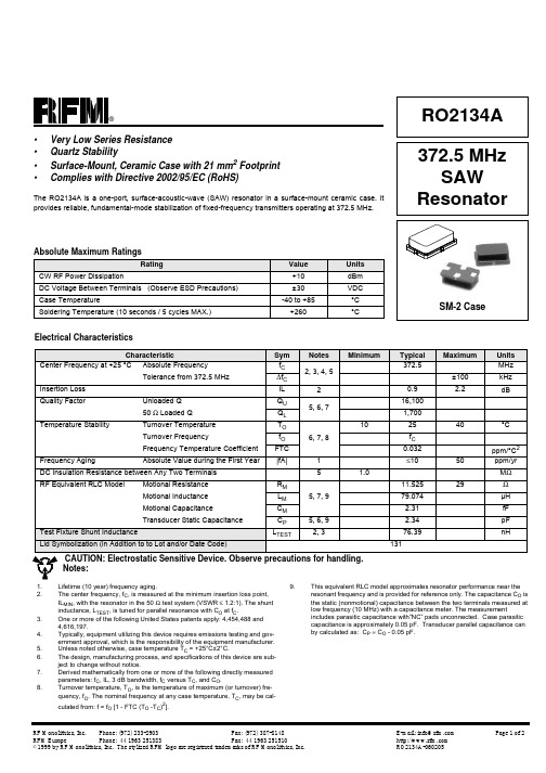
RF Monolithics, Inc.Phone: (972) 233-2903Fax: (972) 387-8148E-mail: info@ Page 1 of 2RFM Europe Phone: 44 1963 251383Fax: 44 1963 251510 ©1999 by RF Monolithics, Inc. The stylized RFM logo are registered trademarks of RF Monolithics, Inc.RO2134A-060205Electrical CharacteristicsCharacteristicSymNotes MinimumTypical Maximum Units Center Frequency at +25 °C Absolute Frequencyf C 2, 3, 4, 5372.5MHz Tolerance from 372.5 MHz∆f C ±100kHz Insertion Loss IL 20.9 2.2dBQuality Factor Unloaded Q Q U 5, 6, 716,10050 Ω Loaded Q Q L 1,700Temperature StabilityTurnover Temperature T O 6, 7, 8102540°CTurnover Frequencyf O f C Frequency Temperature CoefficientFTC 0.032ppm/°C 2Frequency AgingAbsolute Value during the First Year |fA|1≤1050ppm/yr DC Insulation Resistance between Any Two Terminals51.0M ΩRF Equivalent RLC ModelMotional Resistance R M 5, 7, 911.52529ΩMotional Inductance L M 79.074µH Motional CapacitanceC M 2.31fF Transducer Static CapacitanceC P 5, 6, 9 2.34pF Test Fixture Shunt InductanceL TEST2, 376.39nHLid Symbolization (in Addition to to Lot and/or Date Code)131•Very Low Series Resistance •Quartz Stability•Surface-Mount, Ceramic Case with 21mm 2 Footprint •Complies with Directive 2002/95/EC (RoHS)The RO2134A is a one-port, surface-acoustic-wave (SAW) resonator in a surface-mount ceramic case. It provides reliable, fundamental-mode stabilization of fixed-frequency transmitters operating at 372.5MHz.Absolute Maximum RatingsRatingValue Units CW RF Power Dissipation+10dBm DC Voltage Between Terminals (Observe ESD Precautions)±30VDC Case Temperature-40 to +85°C Soldering Temperature (10 seconds / 5 cycles MAX.)+260°C372.5 MHz SAW ResonatorRO2134A CAUTION: Electrostatic Sensitive Device. Observe precautions for handling.Notes:1.Lifetime (10 year) frequency aging.2.The center frequency, f C , is measured at the minimum insertion loss point, IL MIN , with the resonator in the 50Ω test system (VSWR ≤ 1.2:1). The shunt inductance, L TEST , is tuned for parallel resonance with C O at f C .3.One or more of the following United States patents apply: 4,454,488 and 4,616,197.4.Typically, equipment utilizing this device requires emissions testing and gov-ernment approval, which is the responsibility of the equipment manufacturer.5.Unless noted otherwise, case temperature T C =+25°C±2°C.6.The design, manufacturing process, and specifications of this device are sub-ject to change without notice.7.Derived mathematically from one or more of the following directly measured parameters: f C , IL, 3dB bandwidth, f C versus T C , and C O .8.Turnover temperature, T O , is the temperature of maximum (or turnover) fre-quency, f O . The nominal frequency at any case temperature, T C , may be cal-culated from: f =f O [1-FTC (T O -T C )2].9.This equivalent RLC model approximates resonator performance near the resonant frequency and is provided for reference only. The capacitance C O is the static (nonmotional) capacitance between the two terminals measured at low frequency (10MHz) with a capacitance meter. The measurementincludes parasitic capacitance with”NC” pads unconnected. Case parasitic capacitance is approximately 0.05pF. Transducer parallel capacitance can by calculated as: C P ≈C O -0.05pF.372.5 MHz SAW ResonatorRF Monolithics, Inc.Phone: (972) 233-2903Fax: (972) 387-8148E-mail: info@ Page 2 of 2RFM Europe Phone: 44 1963 251383Fax: 44 1963 251510 ©1999 by RF Monolithics, Inc. The stylized RFM logo are registered trademarks of RF Monolithics, Inc.RO2134A-060205Electrical ConnectionsThe SAW resonator is bidirectional and may be in-stalled with either orientation. The two terminals are interchangeable and unnumbered. The callout NC indicates no internal connection. The NC pads assist with mechanical positioning and stability.External grounding of the NC pads is recommend-ed to help reduce parasitic capacitance in the cir-cuit.Typical Test CircuitThe test circuit inductor, L TEST , is tuned to resonate with the static capaci-tance, C O , at F C .Typical Application CircuitsEquivalent LC Mode lTemperature CharacteristicsThe curve shown on the right accounts for resonator contri-bution only and does not in-clude LC component tempera-ture contributions .Typical Circuit Board Land PatternThe circuit board land pattern shown below is one possible design. The op-timum land pattern is dependent on the circuit board assembly process which varies by manufacturer. The distance between adjacent land edges should be at a maximum to minimize parasitic capacitance. Trace lengths from terminal lands to other components should be short and wide to mini-mize parasitic series inductances.Case DesignThe case material is black alumina with contrasting symbolization. All pads are nominally centered with respect to the base and consist of 40 to 70 mi-croinches (min) electroless gold on 60-350 micorinches (min) electrolessnickel.。
ZEN132V130A24LS中文资料(TE Connectivity)中文数据手册「EasyDatasheet - 矽搜」

二极管电容 施工
-40°至+ 85°C -40°至+ 85°C 15KV 4200pF 符合RoHS标准
人体模型
典型@ 1MHz时,1V RMS
T
芯片中文手册,看全文,戳
图 为 PolyZen装 置 PZ8-PZ10基 本 操 作 示 例
-
图 PZ8
35
热插拔响应
ZEN056V130A24LS VS一个 22V / 120W通用电源
表 PZ1
电 气 特 性 PolyZen装 置
(性能额定值 @ 25°C除非另有说明)
coming soon
coming soon
coming soon
coming soon
coming soon
Part Number ZEN056V240A16LS ZEN056V130A24LS ZEN065V130A24LS ZEN098V130A24LS ZEN128V130A24LS ZEN132V130A24LS ZEN164V130A24LS ZEN132V075A48LS
10
PPTC switchesto high resistance
5
VOUT Peak
0
0
0.01
0.02
0.03
0.04
0.05
Time (Sec)
350
VIN
VOUT
300
CURRENT (I ) FLT
POWER
250
Output Voltage remains clamped
200 Power (Watts)
PolyZen器件提供可恢复保护 ,防止多瓦的故障事件 ,只需 要 0.7W的功耗 .在持续的高功率条件下的情况下 ,对设备的 “ 跳闸 ”PPTC元件来限制电流和产生的电压降 .此功能有助于同时 保护齐纳二极管和后续电子 ,有效地提高了二极管的功率处理 能力.
A3144EUA中文资料

30 55 80
30 55 80
20 55 —
over operating temp. range
20 55 80
30 55 80
30 55 80
20 55 —
NOTES: Typical values are at TA = +25°C and VCC = 8 V. BOP = operate point (output turns ON); BRP = release point (output turns OFF); Bhys = hysteresis (BOP - BRP). 1 gauss (G) is exactly equal to 0.1 millitesla (mT). *Complete part number includes a suffix to identify operating temperature range (E- or L-) and package type ( -LT or -UA).
—
0.18
2.0
Units V mV µA mA µs µs
MAGNETIC CHARACTERISTICS in gauss over operating supply voltage range.
Part Numbers*
A3141–
A3142–
A3143–
A3144–
Characteristic
125
150
Dwg. GH-039-1
* Complete part number includes a suffix denoting operating temperature range (E- or L-) and package type ( -LT, -U, or -UA).
SGM321中文资料

MODEL SGM321 SGM358
SGM324
PACKAGE/ORDERING INFORMATION
ORDER NUMBER
SGM321YC5/TR SGM321YN5/TR SGM358YS/TR SGM358YMS/TR
SGM358YP SGM324YS/TR SGM324YTS/TR SGM324YS14/TR SGM324YTS14/TR
The SGM321 is available in SOT23-5 and SC70-5 packages. The SGM358 comes in SO-8,MSOP-8 and PDIP-8 packages. The SGM324 is offered in SO-14, TSSOP-14, TSSOP-16 and SO-16 packages.
11 -INC +INB 5 10 OUT C -INB 6
10 +INT
9 NC
OUT B 7
8 OUT C
TSSOP-16 / SO-16
TSSOP-14/SO-14
Shengbang Microelectronics Co, Ltd Tel: 86/451/84348461
The SGM321/358/324 provide 1MHz bandwidth at a low current consumption of 60µA per amplifier. Very low input bias currents of 10pA, enable SGM321/358/ 324 to be used for integrators, photodiode amplifiers, and piezoelectric sensors. Rail-to-rail inputs and outputs are useful to designers buffering ASIC in single-supply systems.
FAN3214TMX;FAN3213TMX;中文规格书,Datasheet资料
-
Dual Inverting (FAN3213) Dual Non-Inverting (FAN3214)
Internal Resistors Turn Driver Off If No Inputs MillerDrive™ Technology 12ns / 9ns Typical Rise/Fall Times with 2.2nF Load Typical Propagation Delay Under 20ns Matched within 1ns to the Other Channel Double Current Capability by Paralleling Channels Standard SOIC-8 Package Rated from –40°C to +125°C Ambient
Pin Definitions
Pin
1 2 3 2 4 7 5 (FAN3213) 5 (FAN3214) 6 7 (FAN3213) 7 (FAN3214) 8
Name
NC INA GND INA INB OUTA Input to Channel A.
Pin Description
No Connect. This pin can be grounded or left floating.
h
t
t
p
:
/
/
o
n
e
i
c
.
c
o
m
/
FAN3213 / FAN3214 — Dual-4A, High-Speed, Low-Side Gate Drivers
Pin Configurations
FAN3213
AU9254A21中文资料

AU9254A21中⽂资料AU9254 A21USB Hub Controller Technical Reference ManualRevision 1.11997-2003 Alcor Micro Corp.All Rights ReservedCopyright NoticeCopyright 1997 - 2003Alcor Micro Corp.All Rights Reserved.Trademark AcknowledgementsThe company and product names mentioned in this document may be the trademarks or registered trademarks of their manufacturers.DisclaimerAlcor Micro Corp. reserves the right to change this product without notice.Alcor Micro Corp. makes no warranty for the use of its products and bears no responsibility for any errors that appear in this document. Specifications are subject to change without notice.Contact Information:Web site: /doc/8810114908.html/TaiwanAlcor Micro Corp.4F-1, No 200, Kang Chien Rd., Nei Hu,Taipei, Taiwan, R.O.C.Phone: 886-2-8751-1984Fax: 886-2-2659-7723San Clara Office Los Angeles Office2901 Tasman Drive, Suite 206 9400 Seventh St., Bldg. A2Santa Clara, CA 95054 Rancho Cucamonga, CA 91730Phone: (408) 845-9300 Phone: (909) 989-3060Fax: (408) 845-9086 Fax: (909) 944-0464Table of Contents1.0 Introduction (1)1.1. Description (1)1.2. Features (1)2.0 Application Block Diagram (3)3.0 Pin Assignment (5)4.0 System Architecture and Reference Design (10)4.1. AU9254 Block Diagram (10)4.2. Sample Schematics11 (11)5.0 Electrical Characteristics (15)5.1. Absolute Maximum Ratings (15)5.2. Recommended Operating Conditions (15)5.3. General DC Characteristics (15)5.4. DC Electrical Characteristics for 5 volts operation (16)5.5. DC Electrical Characteristics for 3.3 volts operation (16)5.6. Crystal Oscillator Circuit Setup for Characterization (17)5.7. USB Transceiver Characteristics (17)5.8. ESD Test Results (22)5.9. Latch-Up Test Results (23)6.0 Mechanical Information (25)6.1 Normal Size Package (Body Size 209 mil) (25)6.2 Small Size Package (Body Size 150 mil) (27)TABLE OF CONTENTS iTABLE OF CONTENTS i1.0 Introduction1.1. DescriptionThe AU9254A21 is an integrated single chip USB hub controller designed for the emerging industry-standard Universal Serial Bus (USB). The AU9254A21 supports four USB downstream ports. Each downstream port has power switch control, and over-current sensing.Single chip integration makes the AU9254A21 the most cost effective stand-alone USBhub solution available in the market. Downstream ports can be used to connect variousUSB peripheral devices, such as USB printers, modems, scanners, cameras, mice, or joysticks to the system without adding external glue logic.1.2. FeaturesFully compliant with the Universal Serial Bus Specification, version 1.1.USB hub design is compliant with Universal Serial Bus Hub Specification, revision1.1.Single chip integrated USB hub controller with embedded proprietary processor. Supports four bus-powered/self-powered downstream ports.Built-in 3.3v voltage regulator allows single +5V operating voltage, resulting in reduced overall system cost.Runs at 12Mhz frequency.28-pin SSOP package, both normal size (body size 209 mil) and smaller size (body size 150 mil) are available. INTRODUCTION 1This Page Intentionally Left BlankINTRODUCTION 22.0 Application Block DiagramThe AU9254A21 is a single chip 4-port USB hub controller. The upstream port is connected to the USB system. The downstream ports can be used for a mouse, joystick, scanner, printer or other device.KeyboardDIAGRAM 3APPLICATIONBLOCKThis Page Intentionally Left BlankDIAGRAM 4APPLICATIONBLOCKAPPLICATION BLOCK DIAGRAM 53.0 Pin AssignmentThe AU9254A21 is packaged as a 28-pin shrink small outline plastic package (SSOP). The figure on the following page shows the signal names for each of the pins on the chip. Accompanying the figure is the table that describes each of the pin signals.USB1_DP USB1_DM USB_DP USB_DM DP3_OVRCUR DP4_OVRCUR DP3_PWRUP XTAL2XTAL1AGND/GNDO NC DP2_OVRCUR SUSPEND DP1_OVRCURUSB2_DM USB2_DP USB3_DM USB3_DP USB4_DM USB4_DP DP4_PWRUP DP2_PWRUP BUS_PWREDVCC5O/VCC5IK GND5O/GND5IKVCC3V DP1_PWRUP GANGPOWERTable 3-1. Pin Descriptions of Au9254A21, 28-pin SSOPPin Name Input/Output DescriptionPinNo1 USB_DM Input/OutputUSB D- for downstream port 2; add 15K? pull-downto ground.2 USB2_DP Input/OutputUSB D+ for downstream port 2; add 15K? pull-down to ground.3 USB3_DM Input/OutputUSB D- for downstream port 3; add 15K? pull-downto ground.4 USB3_DP Input/OutputUSB D+ for downstream port 3; add 15K? pull-down to ground.5 USB4_DM Input/OutputUSB D- for downstream port 4; add 15K? pull-downto ground.6 USB4_DP Input/OutputUSB D+ for downstream port 4; add 15K? pull-down to ground.7 DP4_PWRUP Output Downstream port 4 power switch control. Active low.8 DP2_PWRUP Output Downstream port 2 power switch control. Active low.9 BUS_PWRED Input Bus power. Low indicates bus-powered.10 VCC5O/VCC5IK Power +5 V power supply.11 GND5O/GND5IK Power Ground.12 VCC3V Power 3.3V output for upstream D+ pull-up.13 DP1_PWRUP Output Downstream port 1 power switch control. Active low.14 GANGPOWER Input Ganged or individual port power selection. Add a 10k pull down for ganged power. 10k pull up forindividual power.15 DP1_OVRCUR Input Downstream port 1 over-current indicator. Active low.SYSTEM ARCHITECTURE AND REFERENCE DESIGN 6SYSTEM ARCHITECTURE AND REFERENCE DESIGN 716 SUSPEND Output Device is in suspended state: Active high. 17DP2_OVRCURInputDownstream port 2 over-current indicator. Active low.18 NC 19 AGND/GNDOPower+5 V power supply.20 XTAL_1 Input Crystal in. 21 XTAL_2 Output Crystal out. 22DP3_PWRUPOutputDownstream port 3 power switch control. Activelow.23 DP4_OVRCUR InputDownstream port 4 over-current indicator. Active low.24 DP3_OVRCUR InputDownstream port 3 over-current indicator. Active low.25 USB_DM Input/OutputUSB D- for upstream.26USB_DP Input/Output USB D+ for upstream port. Need external 1.5K ?pull-up to 3.3V. 27USB1_DM Input/Output USB D- for downstream port 1; add 15K ? pull-downto ground. 28USB1_DP Input/Output USB D+ for downstream port 1; add 15K ? pull-down to ground. This Page Intentionally Left BlankSYSTEM ARCHITECTURE AND REFERENCE DESIGN 84.0 System Architecture andReference Design4.1. AU9254A21 Block DiagramSYSTEM ARCHITECTURE AND REFERENCE DESIGN 94.2 Sample SchematicsSYSTEM ARCHITECTURE AND REFERENCE DESIGN 10SYSTEM ARCHITECTURE AND REFERENCE DESIGN 11SYSTEM ARCHITECTURE AND REFERENCE DESIGN 12SYSTEM ARCHITECTURE AND REFERENCE DESIGN 13This Page Intentionally Left BlankSYSTEM ARCHITECTURE AND REFERENCE DESIGN 14 5.0 Electrical Characteristics5.1. Absolute Maximum RatingsSYMBOL PARAMETER RATING UNITSV CC Power Supply -0.3 to 6.0 VV IN Input Voltage -0.3 to VCC+0.3 VV OUT Output Voltage -0.3 to VCC+0.3 VT STG Storage Temperature -40 to 125 ?C5.2. Recommended Operating ConditionsSYMBOL PARAMETER MIN TYP MAX UNITS5.5V5.0Supply 4.5V CC PowerVoltage 0 V CC V V IN InputTemperature -5 85 O CT OPR Operating5.3. General DC CharacteristicsSYMBOL PARAMETER CONDITIONS MIN TYP MAX UNITS I IL Input low current no pull-up or pull-down-1 1 µAI IH Input high current no pull-up or pull-down-1 1 µAI OZ Tri-state leakage current -10 10 µAcapacitance 4 ρFC IN Inputcapacitance 4 ρFC OUT OutputC BID Bi-directional buffer capacitance 4 ρF CHARACTERISTICS 15ELECTRICAL。
A3144LUA中文资料

OUTPUT SATURATION VOLTAGE
300
I OUT = 20 mA VCC = 4.5–24 V
200
100 RELEASE POINT
100
SATURATION VOLTAGE IN mV
SWITCH POINT IN GAUSS
0
-50
-25
0
25
50
75
100
AMBIENT TEMPERATURE IN °C
—
0.18
2.0
Units V mV µA mA µs µs
MAGNETIC CHARACTERISTICS in gauss over operating supply voltage range.
Part Numbers*
A3141–
A3142–
A3143–
A3144–
Characteristic
Always order by complete part number, e.g., A3141ELT .
元器件交易网
3141 THRU 3144 SENSITIVE HALL-EFFECT SWITCHES FOR HIGH-TEMP. OPERATION
FUNCTIONAL BLOCK DIAGRAM
Min. Typ. Max. Min. Typ. Max. Min. Typ. Max. Min. Typ. Max.
BOP at TA = 25°C
50 100 160 130 180 230 220 280 340
70 — 350
over operating temp. range
30 100 175 115 180 245 205 280 355
OPA132UAG4资料

PACKAGE/ORDERING INFORMATION
For the most current package and ordering information, see the Package Option Addendum located at the end of this data sheet.
OPEN-LOOP GAIN Open-Loop Voltage Gain
RL = 10kΩ, VO = –14.5V to +13.8V RL = 2kΩ, VO = –13.8V to +13.5V RL = 600Ω, VO = –12.8V to +12.5V
FREQUENCY RESPONSE Gain-Bandwidth Product Slew Rate Settling Time: 0.1%
ELECTROSTATIC DISCHARGE SENSITIVITY
This integrated circuit can be damaged by ESD. Texas Instruments recommends that all integrated circuits be handled with appropriate precautions. Failure to observe proper handling and installation procedures can cause damage.
OPA132 op amps are easy to use and free from phase inversion and overload problems often found in common FET-input op amps. Input cascode circuitry provides excellent common-mode rejection and maintains low input bias current over its wide input voltage range. OPA132 series op amps are stable in unity gain and provide excellent dynamic behavior over a wide range of load conditions, including high load capacitance. Dual and quad versions feature completely independent circuitry for lowest crosstalk and freedom from interaction, even when overdriven or overloaded.
MAX3222EEUP中文资料
Battery-Powered Equipment Cell Phones Cell-Phone Data Cables Notebook, Subnotebook, and Palmtop Computers
Applications
Printers Smart Phones xDSL Modems
_______________Ordering Information
PART
TEMP RANGE
PINPACKAGE
PKG CODE
MAX3222ECTP MAX3222ECUP
0°C to +70°C 0°C to +70°C
20 Thin QFNEP** (5mm x 5mm) 20 TSSOP
♦ For Low-Voltage or Data Cable Applications MAX3380E/MAX3381E: +2.35V to +5.5V, 1µA, 2Tx/2Rx, RS-232 Transceivers with ±15kV ESD-Protected I/O and Logic Pins
MAX3222EEPN -40°C to +85°C 18 Plastic DIP —
MAX3232ECAE 0°C to +70°C 16 SSOP
—
MAX3232ECWE 0°C to +70°C 16 Wide SO —
MAX3232ECPE 0°C to +70°C 16 Plastic DIP —
A proprietary low-dropout transmitter output stage delivers true RS-232 performance from a +3.0V to +5.5V power supply, using an internal dual charge pump. The charge pump requires only four small 0.1µF capacitors for operation from a +3.3V supply. Each device guarantees operation at data rates of 250kbps while maintaining RS-232 output levels. The MAX3237E guarantees operation at 250kbps in the normal operating mode and 1Mbps in the MegaBaud™ operating mode, while maintaining RS-232compliant output levels.
UPSD3214AV-24T1中文资料

1/8DATA BRIEFINGJune 2002Complete data available on Data-on-Disc CD-ROM or at .µPSD3200FAMILYFlash Programmable System Devicewith 8032Microcontroller CoreFEATURES SUMMARYs The µPSD3200Family combines a Flash PSD architecture with an 8032microcontroller core The µPSD3200Family of Flash PSDs features dual banks of Flash memory,SRAM,general purpose I/O and programmable logic,supervi-sory functions and access via USB,I 2C,ADC,DDC and PWM channels,and an on-board 8032microcontroller core,with two UARTs,three 16-bit Timer/Counters and one External Interrupt.As with other Flash PSD families,the µPSD3200Family is also in-system program-mable (ISP)via a JTAG ISP interface.sLarge 8KByte SRAM with battery back-up optionsDual bank Flash memories–128KByte or 256KByte main Flash memory –32KByte secondary Flash memorysContent Security–Block access to Flash memorysProgrammable Decode PLD for flexible address mapping of all memories.s High-speed clock standard 8032core (12-cycle)s USB Interface (µPSD3234A-40U6only)s I 2C interface for peripheral connections s Five Pulse Width Modulator (PWM)channels s Standalone Display Data Channel (DDC)s Six I/O ports with up to 50I/O pins s 3000gate PLD with 16macrocells s Supervisor functionss In-System Programming (ISP)via JTAG s Zero-Power Technology sSingle Supply Voltage –4.5to 5.5V –3.0to 3.6VFigure 1.PackagesTQFP52(T)TQFP80(U)µPSD3200FAMILY2/8SUMMARY DESCRIPTION s Dual bank Flash memories–Concurrent operation,read from memory one while erasing and writing the other.In-Appli-cation Programming (IAP)for remote updates –Large 128KByte or 256KByte main Flash memory for application code,operating sys-tems,or bit maps for graphic user interfaces –Large 32KByte secondary Flash memory di-vided in small sectors.Eliminate external EE-PROM with software EEPROM emulation –Secondary Flash memory is large enough for sophisticated communication protocol (USB)during IAP while continuing critical system taskssLarge SRAM with battery back-up option –8KByte SRAM for RTOS,high-level languag-es,communication buffers,and stackssProgrammable Decode PLD for flexible address mapping of all memories–Place individual Flash and SRAM sectors on any address boundary –Built-in page register breaks restrictive 8032limit of 64KByte address space –Special register swaps Flash memory seg-ments between 8032“program”space and “data”space for efficient In-Application Pro-grammingsHigh-speed clock standard 8032core (12-cycle)–40MHz operation at 5V,24MHz at 3.3V –Two UARTs with independent baud rate,three 16-bit Timer/Counters and two External InterruptssUSB Interface (µPSD3234A-40U6only)–Supports USB 1.1Slow Mode (1.5Mbit/s)–Control endpoint 0and interrupt endpoints 1and 2sI 2C interface for peripheral connections –Capable of master or slave operation sFive Pulse Width Modulator (PWM)channels –Four 8-bit PWM units–One 16-bit PWM unitsStandalone Display Data Channel (DDC)–For use in monitor,projector,and TV applica-tions –Compliant with VESA standards DDC1and DDC2B –Eliminate external DDC PROM s Six I/O ports with up to 50I/O pins–Multifunction I/O:GPIO,DDC,I 2C,PWM,PLD I/O,supervisor,and JTAG –Eliminates need for external latches and logics3000gate PLD with 16macrocells–Create glue logic,state machines,delays,etc.–Eliminate external PALs,PLDs,and 74HCxx –Simple PSDsoft Express software ...FreesSupervisor functions–Generates reset upon low voltage or watch-dog time-out.Eliminate external supervisor device –Reset In pinsIn-System Programming (ISP)via JTAG –Program entire chip in 10-25seconds with no involvement of 8032–Allows efficient manufacturing,easy product testing,and Just-In-Time inventory –Eliminate sockets and pre-programmed parts –Program with FlashLINK TM cable and any PCsContent Security–Programmable Security Bit blocks access of device programmers and readerssZero-Power Technology–Memories and PLD automatically reach standby current between input changessPackages –52-pin TQFP–80-pin TQFP:allows access to 8032address/data/control signals for connecting to external peripherals3/8µPSD3200FAMILYFigure 2.µPSD3200Family Functional ModulesAI066194Channel ADC1Mb or 2Mb Main FlashDecode PLD64Kb SRAMCPLD -16MACROCELLSJTAG ISP Port 1Port 32UARTS Interrupt3Timer /Counters256Byte SRAM8051Core Port 3,UART,Intr,Timers,I2CPSD Internal Bus8032Internal BusUSB &TransceiverPort 1,Timers and 2nd UART and ADCDDC w/256Byte SRAM PWM 5Channels Port 4PWM and DDCDedicated USB PinsPort A &B,PLD I/O and GPIOPort D GPIO Port C,JTAG,PLD I/O and GPIOVCC,GND,XTAL256Kb Secondary FlashDedicated PinsI2CPort 0,2Ext.BusReset LogicLVD &WDTBus InterfaceResetD0-D7A0-A15RD,PSEN WR,ALEPage Register PSD MODULEMCU MODULEµPSD3200FAMILY4/8Table 1.80-Pin Package Pin DescriptionNote:PSD Port A and MCU Address/Data bus are added for 80-pin deviceSignal Name In/Out FunctionBasicAlternateAD7-AD0I/O Multiplexed Address/Data bus A11-A8I/O External Address BusRxD2-RxD1I/O General I/O port pinsUART Receive TxD2-TxD1I/O UART TransmitINT1-INT0I/O Interrupt inputs /timer gate controls T2-T0I/O Counter inputsSDA1-SDA2I/OI 2C Bus serial data I/O /DDC interface SCL1-SCL2I/O I 2C Bus clock I/OVSYNC I/O VSYNC input for DDC interface T2EX I/O Timer 2Trigger input ADC3-ADC0I/O ADC Channels inputPWM4-PWM0I/O 8-bit Pulse Width Modulation outputsUSB-,USB+I/O USB I/OAVREF O Reference Voltage input for ADC RD_O Read signal,external bus WR_O Write signal,external bus PSEN_O PSEN signal,external bus ALE O Address Latch signal,external bus RESET_I Active low reset inputXTAL1I Oscillator input pin for system clock XTAL2OOscillator output pin for system clockPA7-P A0I/O General I/O port pins1.PLD Macro-cell outputs2.PLD inputstched Address Out (A0-A7)4.Peripheral I/O mode PB7-PB0I/O General I/O port pins1.PLD Macro-cell outputs2.PLD inputstched Address Out (A0-A7)PC7-PC0I/O General I/O port pins1.PLD Macro-cell outputs2.PLD inputs3.SRAM stand by voltage input (VSTBY)4.JTAG Interface (TDI,TDO,TMS,TCK,TSTA T,TERR)5.SRAM battery-on indicator (PC4)PD2-PD1I/O General I/O port pin1.PLD I/O2.Clock input to PLD and APD3.Chip select to PSD ModuleµPSD3200FAMILY Figure3.TQFP52ConnectionsNote:NC=Not ConnectedPU=Pull-up resistor required(2kΩfor3V devices,7.5kΩfor5V devices)39P1.5/ADC1 38P1.4/ADC0 37P1.3/TXD1 36P1.2/RXD1 35P1.1/T2X 34P1.0/T233V CC32XTAL231XTAL130P3.7/SCL1 29P3.6/SDA1 28P3.5/T127P3.4/T0PD1 PC7 PC6 PC5 PU PC4 NC V CC GND PC3 PC2 PC1 PC0 12345678910111213525154948474645444342414PBPB1PB2PB3PB4PB5VREFGNDRST-INPB6PB7ADC3ADC21415161718192212223242526P4.7/PWM4P4.6/PWM3P4.5/PWM2P4.4/PWM1P4.3/PWMGNDP4.2/DDCVSYNCP4.1/DDCSCLP4./DDCSDAP3./RXDP3.1/TXDP3.2/EXINTP3.3/EXINT1AI05790B5/8µPSD3200FAMILY6/8Figure 4.TQFP80ConnectionsNote: 1.NC =Not ConnectedB-needs a pull-up resistor (see the description of the USB function)60P1.5/ADC1 59P1.4/ADC0 58P1.3/TXD1 57P2.3,A11 56P1.2/RXD1 55P2.2,A10 54P1.1/T2X 53P2.1,A9 52P1.0/T2 51P2.0,A8 50V CC 49XTAL2 48XTAL1 47P0.7,AD7 46P3.7/SCL1 45P0.6,AD6 44P3.6/SDA1 43P0.5,AD5 42P3.5/T1 41P0.4,AD4PD2 P3.3/EXINT1 PD1 PD0,ALE PC7 PC6 PC5 USB- PC4 USB+ NC V CC GND PC3 PC2 PC1 NC P4.7/PWM4 P4.6/PWM3 PC0123 45 6 7 8 9 10 11 12 13 14 15 16 1718 192080 79 78 77 76 75 74 73 72 71 70 69 68 67 66 65 64 63 62 61P B 0P 3.2/E X I N T 0P B 1P 3.1/T X DP B 2P 3.0/R X DP B 3P B 4P B 5N CV R E FG N DR E S E T -I NP B 6P B 7R D ,C N T L 1P 1.7/A D C 3P S E N ,C N T L 2W R ,C N T L 0P 1.6/A D C 22122232425262728293031323334353637383940P A 7 P A 6 P 4.5/P W M 2 P A 5 P 4.4/P W M 1 P A 4 P 4.3/P W M 0 P A 3 G N D P 4.2/D C C V S Y N C P 4.1/D D C S C L P A 2 P 4.0/D D C S D A P A 1 P A 0 A D 0,P 0.0 A D 1,P 0.1 A D 2,P 0.2 A D 3,P 0.3 P 3.4/T 0AI05791µPSD3200FAMILY PART NUMBERINGTable2.Ordering Information SchemeFor a list of available options(speed,package, etc.)or for further information on any aspect of this device,please contact your nearest ST Sales Of-fice.Example:uPSD3234B V–24U6TDevice TypeuPSD=Microcontroller PSDFamily3=8032corePLD Size2=16Macrocells3=32MacrocellsSRAM Size1=16Kbit3=64Kbit5=256KbitMain Flash Memory Size3=1Mbit4=2Mbit5=4MbitIP MixA=USB,I2C,PWM,DDC,ADC,(2)UARTsSupervisor(Reset Out,Reset In,LVD,WD)B=I2C,PWM,DDC,ADC,(2)UARTsSupervisor(Reset Out,Reset In,LVD,WD)Operating Voltageblank=V CC=4.5to5.5VV=V CC=3.0to3.6VSpeed24=24MHz40=40MHzPackageT=52-pin TQFPU=80-pin TQFPTemperature Range1=0to70°C(commercial)6=–40to85°C(industrial)OptionT=Tape&Reel Packing7/8µPSD3200FAMILYInformation furnished is believed to be accurate and reliable.However,STMicroelectronics assumes no responsibility for the consequences of use of such information nor for any infringement of patents or other rights of third parties which may result from its use.No license is granted by implication or otherwise under any patent or patent rights of STMicroelectronics.Specifications mentioned in this publication are subject to change without notice.This publication supersedes and replaces all information previously supplied.STMicroelectronics products are not authorized for use as critical components in life support devices or systems without express written approval of STMicroelectronics.The ST logo is registered trademark of STMicroelectronicsAll other names are the property of their respective owners©2002STMicroelectronics-All Rights ReservedSTMicroelectronics group of companiesAustralia-Brazil-Canada-China-Finland-France-Germany-Hong Kong-India-Israel-Italy-Japan-Malaysia-Malta-Morocco-Singapore-Spain-Sweden-Switzerland-United Kingdom-United States.8/8。
CSC-246AE数字式备用电源自投入装置说明书-V2.01S

CSC-246A/E数字式备用电源自投入装置说明书CSC-246A/E数字式备用电源自投入装置说明书CD2012075编制: 张华年校核:王彦辉标准化审查: 李连昌审定:邹卫华出版号:V2.01S文件代号:0SF.457.016出版日期:2012年3月版权所有:北京四方继保自动化股份有限公司注:本公司保留对此说明书修改的权利。
如果产品与说明书有不符之处,请您及时和我公司联系,我们将为您提供相应的服务。
技术支持服务热线电话:传真:重要提示感谢您使用北京四方继保自动化股份有限公司的产品。
为了安全、正确、高效地使用本装置,请您务必注意以下重要提示:1)本说明书仅适用于CSC-246A/E数字式备用电源自投入装置,其配套的程序版本为V2.01及其以上兼容版本。
2)请仔细阅读本说明书,并按照说明书的规定整定、调试和操作。
如有随机资料,请以随机资料为准。
3)为防止装置损坏,严禁带电插拔装置各插件、触摸印制电路板上的芯片和器件。
4)请使用合格的测试仪器和设备对装置进行试验和检测。
5)装置如出现异常或需维修,请及时与本公司服务热线联系。
6)本装置的出厂操作密码是:8888。
目录第一篇装置技术说明 (4)1概述 (4)1.1 适用范围 (4)1.2 装置主要特点 (4)1.3 装置执行的标准 (6)2技术条件 (7)2.1 环境条件 (7)2.2 电气绝缘性能 (7)2.3 机械性能 (7)2.4 电磁兼容性 (7)2.5 安全性能 (8)2.6 功率消耗 (8)2.7 输出触点容量 (8)2.8 装置主要技术参数 (8)3装置硬件 (10)3.1 装置结构 (10)3.2 装置外观图 (10)3.3 装置插件布置图 (11)3.4 采样插件 (11)3.5 CPU插件 (11)3.6 通信管理插件 (11)3.7 开入插件 (12)3.8 开出插件 (12)3.9 操作插件 (12)3.10 电源插件 (12)4装置软件 (13)4.1 保护程序整体结构 (13)4.2 数字化功能 (13)4.3保护功能 (13)4.4 零序电流保护 (13)4.5 过电流保护 (14)4.6 过负荷联切功能 (15)4.7 备投功能概述 (15)4.8 遥控开出 (19)4.9 智能终端及控制回路检测 (19)4.10 MU异常对保护的影响 (19)第二篇用户使用说明 (20)5开箱检查 (20)6安装调试 (20)6.1 安装 (20)6.2 通电前的检查 (20)6.3 装置通电检查 (21)7定值清单及整定说明 (29)7.1 CSC-246A/E装置定值清单及其整定说明 (29)8装置端子说明 (33)8.1 开入端子说明 (33)8.2 电源插件端子说明 (33)9人机接口及其操作 (34)9.1 装置面板布置图 (34)9.2 正常运行显示 (34)9.3 装置模拟量显示含义 (35)9.4 装置菜单结构 (36)10运行维护 (38)10.1 装置投运前检查 (38)10.2 运行中的注意事项 (38)10.3 设备更换保护软件或保护CPU板后的操作 (39)10.4 设备更换MASTER软件或MASTER板后的操作 (39)10.5 定值固化方式、定值区切换方式、打印方式等的说明 (39)11保护报文汇总 (41)11.1 装置告警信息 (41)11.2 运行异常信息 (41)11.3 GOOSE和MU告警信息 (42)12运输、贮存 (43)13订货须知 (43)14附录1:字符和中文字符集 (44)14.2 ASCII 16进制字符表 (44)14.3 中文字符表 (45)15附图 (52)15.1 CPU简化原理图 (52)15.2 MASTER板简化原理图 (53)15.3 开出2插件原理图 (54)15.4 操作插件原理图 (55)15.5 电源插件原理图 (56)15.6 CSC-246A/E装置背板端子图 (57)第一篇装置技术说明1概述1.1适用范围CSC-246A/E数字式备用电源自投入装置适用于数字化变电站。
SGM321中文资料
SGM321中文资料SGM321 SGM358 SGM3241MHz, 60μA, Rail-to-Rail I/O CMOS Operational AmplifierELECTRICAL CHARACTERISTICS : V S = +5V (At R L = 100kΩ connected to Vs/2,and V OUT= Vs/2, unless otherwise noted)Specifications subject to change without notice. PACKAGE/ORDERING INFORMATIONMODEL ORDERNUMBERPACKAGEDESCRIPTIONPACKAGEOPTIONMARKINGINFORMATIONSGM321YC5/TR SC70-5 Tape and Reel, 3000 321 SGM321SGM321YN5/TR SOT23-5 Tape and Reel, 3000 321SGM358YS/TR SO-8Tape and Reel, 2500 SGM358YSSGM358YMS/TR MSOP-8 Tape and Reel, 3000 SGM358YMS SGM358SGM358YP PDIP-8 Tube,50 SGM358YPSGM324YS/TR SO-16Tape and Reel, 2500 SGM324YSSGM324YTS/TR TSSOP-16 Tape and Reel, 3000 SGM324YTS SGM324YS14/TR SO-14 Tape and Reel, 2500 SGM324YS14 SGM324SGM324YTS14/TR TSSOP-14 Tape and Reel, 3000 SGM324YTS14ABSOLUTE MAXIMUM RATINGS Supply Voltage, V+ to V- . . . . . . . . . . . . . . . . . . . . . 7.5 V Common-Mode Input Voltage . . . . . . . . . . . . . . . . . . . . (–V S) – 0.5 V to (+V S )+0.5V Storage Temperature Range . . . . . . . . .–65℃ to +150℃Junction Temperature . . . . . . . . . . . . . . . .. . . . . . . .160℃Operating Temperature Range . . . . . . . –45℃ to +85℃Package Thermal Resista nce @ T A = 25℃SC70-5, θJA................................................................ 333/W℃SOT23-5, θJA.............................................................. 190/W℃SO-8, θJA......................................................................125/W℃MSOP-8, θJA.............................................................. 216/W℃SO-16, θJA..................................................................... 82/W℃TSSOP-16, θJA............................................................ 105/W℃Lead Temperature Range (Soldering 10 sec).....................................................260℃ESD SusceptibilityHBM (4000V)MM (400V)NOTES1. Stresses above those listed under Absolute Maximum Ratings may cause permanent damage to the device. This is a stress rating only; functional operation of the device at these or any other conditions above those indicated in the operational section of this specification is not implied. Exposure to absolute maximum rating conditions for extended periods may affect device reliability. CAUTIONThis integrated circuit can be damaged by ESD. Shengbang Micro-electronics recommends that all integrated circuits be handled with appropriate precautions. Failure to observe proper handling and installation procedures can cause damage.ESD damage can range from subtle performance degradation to complete device failure. Precision integrated circuits may be more susceptible to damage because very small parametric changes could cause the device not to meet its published specifications.TYPICAL PERFORMANCE CHARACTERISTICSAt T A = +25℃, V S = +5V , and R L = 100k Ω conne cted to Vs/2,unless otherwise noted.Small-Signal Step Response Large-Signal Step Response2μs/div 10μs/div20m V /d i v500m V /d i vG = +1C L = 100pF R L = 100K ?G = +1C L = 100pF R L = 100K ?TYPICAL PERFORMANCE CHARACTERISTICS At T A = +25℃, V S = +5V, and R L = 100kΩconnected to Vs/2,unless otherwise noted.TYPICAL PERFORMANCE CHARACTERISTICSAt T A = +25℃, V S = +5V , and R L = 100k Ω connected to Vs/2,unless otherwise noted.Overload Recovery TimeTime(2μs/div)Vs = 5V G = -5 V IN= 500mV 2.5V0V 500mV0VAPPLICATION NOTESDriving Capacitive LoadsThe SGM3XX can directly drive 250pF in unity-gain without oscillation. The unity-gain follower (buffer) is the most sensitive configuration to capacitive loading. Direct capacitive loading reduces the phase margin of amplifiers and this results in ringing or even oscillation. Applications that require greater capacitive drive capability should use an isolation resistor between the output and the capacitive load like the circuit in Figure 1. The isolation resistor R ISO and the load capacitor C L form a zero to increase stability. The bigger the R ISO resistor value, the more stable V OUT will be. Note that this method results in a loss of gain accuracy because R ISO forms a voltage divider with the R LOAD.V IN V OUTFigure 1. Indirectly Driving Heavy Capacitive LoadAn improvement circuit is shown in Figure 2, It provides DC accuracy as well as AC stability. R F provides the DC accuracy by connecting the inverting signal with the output, C F and R Iso serve to counteract the loss of phase margin by feeding the high frequency component of the output signal back to the amplifier’s inverting input, thereby preserving phase margin inthe overall feedback loop.V IN V OUTFigure 2. Indirectly Driving Heavy Capacitive Load with DC AccuracyFor no-buffer configuration, there are two others ways to increase the phase margin: (a) by increasing the amplifier’s gain or (b) by placing a capacitor in parallel with the feedback resistor to counteract the parasitic capacitance associated with inverting node. Power-Supply Bypassing and Layout The SGM3XX family operates from either a single +2.5V to +5.5V supply or dual ±1.25V to ±2.75V supplies. For single-supply operation, bypass the power supply V DD with a 0.1μF ceramic capacitor which should be placed close to the V DD pin. For dual-supply operation, both the V DD and the V SS supplies should be bypassed to ground with separate 0.1μF ceramic capacitors.2.2μF tantalum capacitor can be added for better performance.VnVpV SSV SS(GND)Figure 3. Amplifier with Bypass CapacitorsTypical Application Circuits Differential AmplifierThe circuit shown in Figure 4 performs the difference function. If the resistors ratios are equal ( R4 / R3 = R2 / R1 ), then V OUT = ( Vp –Vn ) × R2 / R1 + Vref.Vn VpOUT Figure 4. Differential AmplifierInstrumentation AmplifierThe circuit in Figure 5 performs the same function as that in Figure 4 but with the high input impedance.Vn VpV OUT Figure 5. Instrumentation AmplifierLow Pass Active FilterThe low pass filter shown in Figure 6 has a DC gain of ( - R2 / R1 ) and the –3dB corner frequency is 1/2πR2C. Make sure the filter is within the bandwidth of the amplifier. The Large values of feedback resistors can couple with parasitic capacitance and cause undesired effects such as ringing or oscillation in high-speed amplifiers. Keep resistors value as low as possible and consistent with output loading consideration.V INV OUTFigure 6. Low Pass Active FilterPACKAGE OUTLINE DIMENSIONS SC70-5PACKAGE OUTLINE DIMENSIONS SOT23-5PACKAGE OUTLINE DIMENSIONS SO-8PACKAGE OUTLINE DIMENSIONS MSOP-8PACKAGE OUTLINE DIMENSIONS PDIP-8PACKAGE OUTLINE DIMENSIONS SO-14PACKAGE OUTLINE DIMENSIONS SO-16PACKAGE OUTLINE DIMENSIONS TSSOP-14PACKAGE OUTLINE DIMENSIONS TSSOP-16REVISION HISTORYLocation Page 11/06—Data Sheet changed from REV.A to REV.BChanges to ABSOLUTE MAXIMUM ATINGS . . . . . . . . . . . . . . . . . . . . . . . . . . . . . . . .. . . . . . . . . . . . . . . . . . . . . . . . . . .. . . . . . . 3 04/07— Data Sheet changed from REV.B to REV.CAdds Output Voltage Swing from Rail test condition. . . . . . . . . . . . . . . . . . . . . . . . . . . . . .. . . . . . . . . . . . . . . . . . . . . . . . . . .. . . . . . 206/07— Data Sheet changed from REV.C to REV. DAdds SO-14 and TSSOP-14 Packages . . . . . . . . . . . . . . . . . . . . . . .. . . . . . . . . . . . . . . . . . . . . . . . . .. . . . . . . . . . . .. . .1, 3, 14, 16Shengbang Microelectronics Co, LtdUnit 3, ChuangYe PlazaNo.5, TaiHu Northern Street, YingBin Road CentralizedIndustrial ParkHarbin Development ZoneHarbin, HeiLongJiang 150078P.R. ChinaTel.: 86-451-84348461Fax: 86-451-84308461。
AOD413A中文资料
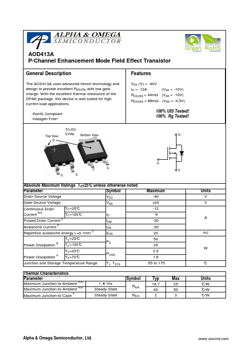
A: The value of RθJA is measured with the device in a still air environment with T A =25° C. The power dissipation P DSM and current rating IDSM are based on TJ(MAX)=150° C, using t ≤ 10s junction-to-ambient thermal resistance. B. The power dissipation PD is based on TJ(MAX)=175° C, using junction-to-case thermal resistance, and is more useful in setting the upper dissipation limit for cases where additional heatsinking is used. C: Repetitive rating, pulse width limited by junction temperature TJ(MAX)=175° C. D. The RθJA is the sum of the thermal impedence from junction to case RθJC and case to ambient. -20 E. The static characteristics in Figures 1 to 6 are obtained using <300 µs pulses, duty cycle 0.5% max. 20 F. These curves are based on the junction-to-case thermal impedence which is measured with the device mounted to a large heatsink, assuming C. The SOA curve provides a single pulse ratin g. a maximum junction temperature of TJ(MAX)=175° G. These tests are performed with the device mounted on 1 in2 FR-4 board with 2oz. Copper, in a still air environment with TA=25° C. H. The maximum current rating is limited by bond-wires. *This device is guaranteed green after data code 8X11 (Sep 1ST 2008). Rev1: Oct 2008 COMPONENTS IN LIFE SUPPORT DEVICES OR SYSTEMS ARE NOT AUTHORIZED. AOS DOES NOT ASSUME ANY LIABILITY ARISING OUT OF SUCH APPLICATIONS OR USES OF ITS PRODUCTS. AOS RESERVES THE RIGHT TO IMPROVE PRODUCT DESIGN, FUNCTIONS AND RELIABILITY WITHOUT NOTICE.
2SA2151A中文资料
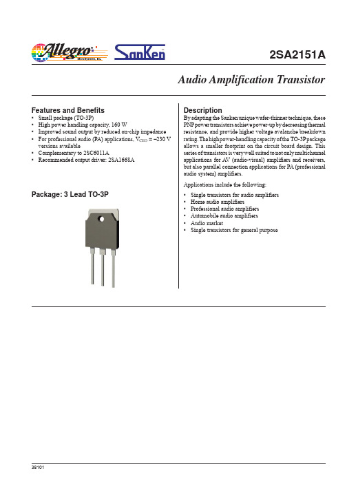
2SA2151ADescriptionBy adapting the Sanken unique wafer-thinner technique, thesePNP power transistors achieve power-up by decreasing thermalresistance, and provide higher voltage avalanche breakdownrating. The high power-handling capacity of the TO-3P packageallows a smaller footprint on the circuit board design. Thisseries of transistors is very well suited to not only multichannelapplications for A V (audio-visual) amplifiers and receivers,but also parallel connection applications for PA (professionalaudio system) amplifiers.Applications include the following:▪Single transistors for audio amplifiers▪Home audio amplifiers▪Professional audio amplifiers▪Automobile audio amplifiers▪ Audio market▪Single transistors for general purposeFeatures and Benefits▪Small package (TO-3P)▪High power handling capacity, 160 W▪Improved sound output by reduced on-chip impedance▪For professional audio (PA) applications, V CEO = –230 Vversions available▪Complementary to 2SC6011A▪Recommended output driver: 2SA1668AAudio Amplification TransistorPackage: 3 Lead TO-3PAudio Amplification Transistor2SA2151A ELECTRICAL CHARACTERISTICS at T A = 25°CCharacteristicSymbol Test ConditionsMin.Typ.Max.Unit Collector-Cutoff Current I CBO V CB = –230 V –––10μA Emitter Cutoff Current I EBO V EB = –6 V –––10μA Collector-Emitter Voltage V (BR)CEOI C = –50 mA –230––V DC Current Transfer Ratio*h FE V CE = –4 V, I C = –3 A 50–180–Collector-Emitter Saturation Voltage V CE(sat)I C = –5 A, I B = –0.5 A –––0.5V Cutoff Frequency f T V CE = –12 V, I E = 0.5 A–20–MHz Output CapacitanceC OBV CB = –10 V, I E = 0 A, f = 1 MHz–450–pF*h FE rating: 50 to 100 (O brand on package), 70 to 140 (P), 90 to 180 (Y).ABSOLUTE MAXIMUM RATINGS at T A = 25°CCharacteristicSymbol Rating Unit Collector-Base Voltage V CBO –230V Collector-Emitter Voltage V CEO –230V Emitter-Base Voltage V EBO –6V Collector Current I C –15A Base CurrentI B –4A Collector Power Dissipation P C 160W Junction Temperature T J 150°C Storage TemperatureT stg–55 to150°CSELECTION GUIDEPart NumberTypeh FE RatingPacking2SA2151A*PNPRange O: 50 to 100Bulk, 100 pieces Range P: 70 tp 140Range Y: 90 to 180*Specify h FE range when ordering. If no h FE range is specified, order will be fulfilled with either or both range O and range Y , depending upon availability.Audio Amplification Transistor2SA2151APerformance Characteristics–I C (A )I C vs.V CEI C vs.V BE–V CE =4V Continuous–I C (A )05h FE vs. I C–V CE =4V Continuous–I C (A)h F Et (ms)Audio Amplification Transistor2SA2151A–I C (A )–V CE (V)Safe Operating AreaT A = 25°C, single pulse, no heatsink, natural cooling 102030f T vs. I E –V CE = 12 V Continuousf T (M H z )I E (A)P C vs. T AT A (°C)Performance Characteristics, continuedAudio Amplification Transistor2SA2151ATerminal core material: CuTerminal treatment: Ni plating and solder dip Heat sink core material: Cu Heat sink treatment: Ni plating Leadform number: 100Dimensions in millimetersBranding codes (exact appearance at manufacturer discretion):1st line, type: A2151A2nd line, lot: YM H Where: Y is the last digit of the year of manufacture M is the month (1 to 9, O, N, D )H is the h FE rating (O, P , or Y ; for values see footnote, Electrical Characteristics table)PACKAGE OUTLINE DRAWING, TO-3PLeadframe plating Pb-free. Device composition includes high-temperature solder (Pb >85%), which is exempted from the RoHS directive.Audio Amplification Transistor 2SA2151ABecause reliability can be affected adversely by improper storage environments and handling methods, please observe the following cautions.Cautions for Storage• Ensure that storage conditions comply with the standard temperature (5°C to 35°C) and the standard relative humidity(around 40 to 75%); avoid storage locations that experienceextreme changes in temperature or humidity.• Avoid locations where dust or harmful gases are present and avoid direct sunlight.• Reinspect for rust on leads and solderability of products that have been stored for a long time.Cautions for Testing and HandlingWhen tests are carried out during inspection testing and otherstandard test periods, protect the products from power surgesfrom the testing device, shorts between adjacent products, and shorts to the heatsink.Remarks About Using Silicone Grease with a Heatsink• When silicone grease is used in mounting this product on a heatsink, it shall be applied evenly and thinly. If more siliconegrease than required is applied, it may produce stress.• Coat the back surface of the product and both surfaces of the insulating plate to improve heat transfer between the product and the heatsink.• Volatile-type silicone greases may permeate the product and produce cracks after long periods of time, resulting in reducedheat radiation effect, and possibly shortening the lifetime of theproduct.• Our recommended silicone greases for heat radiation purposes, which will not cause any adverse effect on the product life, areindicated below:Type SuppliersG746Shin-Etsu Chemical Co., Ltd.YG6260GE Toshiba Silicone Co., Ltd.SC102Dow Corning Toray Silicone Co., Ltd.Heatsink Mounting Method• Torque When Tightening Mounting Screws. Thermal resistance increases when tightening torque is low, and radiation effects are decreased. When the torque is too high, the screw can strip, the heatsink can be deformed, and distortion can arise in the product frame.To avoid these problems, observe the recommended tightening torques for this product package type, TO-3P (MT-100): 0.686 to 0.882 N•m (7 to 9 kgf•cm).• Diameter of Heatsink Hole: < 4 mm. The defl ection of the press mold when making the hole may cause the case material to crack at the joint with the heatsink. Please pay special attention for this effect.Soldering• When soldering the products, please be sure to minimize the working time, within the following limits:260±5°C 10 s350±5°C 3 s• Soldering iron should be at a distance of at least 1.5 mm from the body of the productsElectrostatic Discharge• When handling the products, operator must be grounded.Grounded wrist straps worn should have at least 1 MΩ ofresistance to ground to prevent shock hazard.• Workbenches where the products are handled should begrounded and be provided with conductive table and floor mats.• When using measuring equipment such as a curve tracer, the equipment should be grounded.• When soldering the products, the head of soldering irons or the solder bath must be grounded in other to prevent leak voltagesgenerated by them from being applied to the products.• The products should always be stored and transported in our shipping containers or conductive containers, or be wrapped inaluminum foil.Audio Amplification Transistor 2SA2151AThe products described herein are manufactured in Ja p an by Sanken Electric Co., Ltd. for sale by Allegro MicroSystems, Inc.Sanken and Allegro reserve the right to make, from time to time, such de p ar t ures from the detail spec i f i c a t ions as may be re q uired to per m it im-p rove m ents in the per f or m ance, reliability, or manufacturability of its prod u cts. Therefore, the user is cau t ioned to verify that the in f or m a t ion in this publication is current before placing any order.When using the products described herein, the ap p li c a b il i t y and suit a bil i t y of such products for the intended purpose shall be reviewed at the users responsibility.Although Sanken undertakes to enhance the quality and reliability of its prod u cts, the occurrence of failure and defect of semi c on d uc t or products at a certain rate is in e v i t a b le.Users of Sanken products are requested to take, at their own risk, preventative measures including safety design of the equipment or systems against any possible injury, death, fires or damages to society due to device failure or malfunction.Sanken products listed in this publication are designed and intended for use as components in general-purpose electronic equip m ent or apparatus (home ap p li a nc e s, office equipment, tele c om m u n i c a t ion equipment, measuring equipment, etc.). Their use in any application requiring radiation hardness assurance (e.g., aero s pace equipment) is not supported.When considering the use of Sanken products in ap p li c a t ions where higher reliability is re q uired (transportation equipment and its control systems or equip m ent, fire- or burglar-alarm systems, various safety devices, etc.), contact a company sales representative to discuss and obtain written confirmation of your spec i f i c a t ions.The use of Sanken products without the written consent of Sanken in applications where ex t reme l y high reliability is required (aerospace equip-ment, nuclear power-control stations, life-support systems, etc.) is strictly prohibited.The information in c lud e d herein is believed to be accurate and reliable. Ap p li c a t ion and operation examples described in this pub l i c a t ion are given for reference only and Sanken and Allegro assume no re s pon s i b il i t y for any in f ringe m ent of in d us t ri a l property rights, intellectual property rights, or any other rights of Sanken or Allegro or any third party that may result from its use.Anti radioactive ray design is not considered for the products listed herein.Copyright © 2006 Allegro MicroSystems, Inc.This datasheet is based on Sanken datasheet SSE-23014。
MAX3243EEAI-T中文资料

MAX3221E/MAX3223E/MAX3243E †
Ordering Information
PART MAX3221ECTE MAX3221ECUE MAX3221ECAE MAX3221EEAE MAX3221EETE MAX3221EEUE MAX3223ECPP MAX3223ECAP MAX3223ECUP MAX3223ECTP MAX3223EEPP MAX3223EEAP MAX3223EEUP MAX3223EETP TEMP RANGE 0°C to +70°C 0°C to +70°C 0°C to +70°C PINPACKAGE 16 Thin QFN-EP (5mm x 5mm) 16 TSSOP 16 SSOP 16 Thin QFN-EP (5mm x 5mm) 20 Plastic DIP 20 SSOP 20 TSSOP PKG CODE T1655-2 — — — T1655-2 — — — —
Pin Configurations appear at end of data sheet. Typical Operating Circuits appear at end of data sheet.
MAX3223E MAX3243E
AutoShutdown and ntegrated Products, Inc.
VCC to GND ..............................................................-0.3V to +6V V+ to GND (Note 1) ..................................................-0.3V to +7V V- to GND (Note 1) ...................................................+0.3V to -7V V+ + |V-| (Note 1) .................................................................+13V Input Voltages T_IN, EN, FORCEON, FORCEOFF to GND ............-0.3V to +6V R_IN to GND ......................................................................±25V Output Voltages T_OUT to GND................................................................±13.2V R_OUT, R2OUTB, INVALID to GND .........-0.3V to (VCC + 0.3V) Short-Circuit Duration T_OUT to GND .........................................................Continuous Continuous Power Dissipation (TA = +70°C) 16-Pin SSOP (derate 7.14mW/°C above +70°C) ...........571mW 16-Pin TSSOP (derate 9.4mW/°C above +70°C) ........754.7mW 16-Pin TQFN (derate 20.8mW/°C above +70°C) ......1666.7mW 20-Pin Plastic DIP (derate 11.11mW/°C above +70°C)....889mW 20-Pin SSOP (derate 8.00mW/°C above +70°C) ...........640mW 20-Pin TSSOP (derate 10.9mW/°C above +70°C) .........879mW 20-Pin TQFN (derate 21.3mW/°C above +70°C) ......1702.1mW 28-Pin SSOP (derate 9.52mW/°C above +70°C)............762mW 28-Pin TSSOP (derate 12.8mW/°C above +70°C) .......1026mW Operating Temperature Ranges MAX32_ _EC_ _ ....................................................0°C to +70°C MAX32_ _EE_ _..................................................-40°C to +85°C Storage Temperature Range .............................-65°C to +160°C Lead Temperature (soldering, 10s) .................................+300°C
A3212中文规格书-Datasheet资料

A3212中文规格书-Datasheet资料DFN (EH)Micropower, UltrasensitiveHall-Ef f ect SwitchesA3211 and A3212 DFN (EL)This device includes on a single silicon chip a Hall-voltage gen-erator, small-signal amplifier, chopper sta b i l i z a t ion, a latch, and a MOSFET output. Advanced CMOS processing is used to take advantage of low-voltage and low-power requirements, compo-nent matching, very low input-offset errors, and small component geometries.Four package styles provide magnetically op t i m ized solutions for most ap p li c a t ions. Miniature low-profile surface-mount package types EH and EL (0.75 and 0.50 mm nominal height) are leadless, LH is a 3-pin low-profile SMD, and UA is a three-pin SIP for through-hole mount i ng. Packages are lead (Pb) free (suffix, –T )with 100% matte tin plated leadframes.Description (continued)Absolute Maximum RatingsCharacteristicSymbol NotesRating Units Supply Voltage V DD 5V Magnetic Flux Density B UnlimitedG Output Off Voltage V OUT 5V Output CurrentI OUT 1mA Operating Ambient Temperature T A Range E –40 to 85oC Range L–40 to 150oC Maximum Junction T emperature T J (max)165oC Storage TemperatureT stg–65 to 170oCSelection GuidePart Number Packing 1PackageAmbient TemperatureT A (°C)State in Magnetic FieldA3211EEHLT–T 23000 pieces per reel 2 mm x 3 mm, 0.75 mm nominal height DFN –40 to 85OffA3211EELLT–T 23000 pieces per reel 2 mm x 2 mm, 0.50 mm nominal height DFN A3211ELHLT–T 3000 pieces per reel 3-pin surface mount SOT23WA3212EEHLT–T 23000 pieces per reel 2 mm x 3 mm, 0.75 mm nominal height DFN –40 to 85OnA3212EELLT–T 23000 pieces per reel 2 mm x 2 mm, 0.50 mm nominal height DFN A3212ELHLT–T 3000 pieces per reel 3-pin surface mount SOT23W A3212EUA–T 500 pieces per bulk bag SIP-3 through holeA3212LLHLT–T 3000 pieces per reel 3-pin surface mount SOT23W –40 to 150A3212LUA–T500 pieces per bulk bagSIP-3 through hole1Contact Allegro for additional packaging and handlingoptions.2Allegro products sold in DFN package types are not intended for automotive applications.Package Suffix ‘UA’ Pinning(SIP)Package Suffix ‘LH’ Pinning(SOT23W)Dwg. PH-016-1S U P P L YG R O U N DO U T P U TELECTRICAL CHARACTERISTICS over operating voltage and temperature range (unless otherwise specified).Characteristic Symbol Test ConditionsLimitsMin.Typ.*Max.UnitsSupply Voltage Range V DD Operating 2.5 2.75 3.5V Output Leakage Current I OFF V OUT = 3.5 V, Output off–<1.0 1.0μA Output On Voltage V OUT I OUT = 1 mA, V DD = 2.75 V–100300mV Awake Time t awake–4590μs Period t period–4590ms Duty Cycle d.c.–0.1–% Chopping Frequency f C–340–kHz Supply Current I DD(EN)Chip awake (enabled)––2.0mA I DD(DIS)Chip asleep (disabled)––8.0μAI DD(AVG)V DD = 2.75 V–5.110μAV DD = 3.5 V–6.710μA* Typical data is at T A = 25°C and V DD = 2.75 V, and is fordesign information only.A3211 MAGNETIC CHARACTERISTICS over operating voltage range (unless otherwise specified)Characteristic Symbol Test ConditionsLimitsMin.Typ.Max.UnitsOver Temperature Range E: T A = –40°C to 85°COperate Points B OPS South pole to branded side; B > B OP, V OUT = High (Output Off)–3755G B OPN North pole to branded side; B > B OP, V OUT = High (Output Off)–55–40–GRelease Points B RPS South pole to branded side; B < B RP, V OUT = Low (Output On)1031–G B RPN North pole to branded side; B < B RP, V OUT = Low (Output On)––34–10GHysteresis B HYS|B OPx - B RPx|– 5.9–G NOTES: 1. Negative flux densities are defined as less than zero (algebraic convention),i.e., -50 G is less than +10 G.2.B OPx = operate point (output turns off); B RPx = release point (output turns on).3. Typical Data is at T A = +25°C and V DD = 2.75 V and is for design information only.4. 1 gauss (G) is exactly equal to 0.1 millitesla (mT).Characteristic Symbol Test ConditionsLimitsMin.Typ.Max.UnitsOver Temperature Range E: T A = –40°C to 85°COperate Points B OPS South pole to branded side; B > B OP, V OUT = Low (Output On)–3755G B OPN North pole to branded side; B > B OP, V OUT = Low (Output On)–55–40–GRelease Points B RPS South pole to branded side; B < B RP, VOUT = High (Output Off)1031–G B RPN North pole to branded side; B < B RP, V OUT = High (Output Off)––34–10GHysteresis B HYS|B OPx - B RPx|–5.9–G Over Temperature Range L: T A = –40°C to 150°COperate Points B OPS South pole to branded side; B > B OP, V OUT = Low (Output On)–3765G B OPN North pole to branded side; B > B OP, V OUT = Low (Output On)–65–40–GRelease Points B RPS South pole to branded side; B < B RP, V OUT = High (Output Off)1031–G B RPN North pole to branded side; B < B RP, V OUT = High (Output Off)––34–10GHysteresis B HYS|B OPx - B RPx|– 5.9–G NOTES: 1. Negative flux densities are defined as less than zero (algebraic convention),i.e., -50 G is less than +10 G.2.B OPx = operate point (output turns on); B RPx = release point (output turns off).3. Typical Data is at T A = +25°C and V DD = 2.75 V and is for design information only.4. 1 gauss (G) is exactly equal to 0.1 millitesla (mT).A3212 MAGNETIC CHARACTERISTICS over operating voltage range (unless otherwise specified)SUPPLY CURRENTFUNCTIONAL DESCRIPTIONChopper-Stabilized Technique. The Hall element can be considered as a resistor array similar to a Wheatstone bridge. A large portion of the offset is a result of the mismatching of theseresistors. These devices use a proprietary dynamic offset cancel-lation technique, with an internal high-frequency clock to reduce the residual offset voltage of the Hall element that is normally caused by device overmolding, temperature de p en d en c ies, and thermal stress. The chopper-stabilizing technique cancels the mismatching of the resistor circuit by changing the direction of the current flowing through the Hall plate using CMOS switches and Hall voltage measurement taps, while maintaing the Hall-voltage signal that is induced by the external magnetic flux. The signal is then captured by a sample-and-hold circuit and further processed using low-offset bipolar circuitry. This technique produces devices that have an extremely stable quiescent Hall output voltage, are immune to thermal stress, and have precise recoverability after temperature cycling. A relatively high sam-pling frequency is used for faster signal processing capability can be processed.More detailed descriptions of the circuit operation can be found in: Technical Paper STP 97-10, Monolithic Magnetic Hall Sensing Using Dynamic Quadrature Offset Cancellation and Technical Paper STP 99-1, Chopper-Stabilized Amplifiers With A Operation. The output of the A3212 switches low (turns on)the operate point B OPS (or is less than B OPN output is capable of sinking up to 1 mA and the output voltage is V OUT(ON). When the magnetic field is reduced below the release point B RPS (or increased above B RPN switches high (turns off). The dif f er e and release points is the hysteresis (B hys ) of the device. This built-in hysteresis allows clean switching of the output even in the presence of external mechanical vibration andelectrical to the right.As used here, negative flux densities are defined as less than zero (algebraic convention), i.e., -50 G is less than +10 G.Applications. Allegro's pole-independent processing tech-nique allows for operation with either a north pole or south pole magnet orientation, enhancing the manufacturability of the device. The state-of-the-art technology provides the same output polarity for either pole face.It is strongly recommended that an external bypass ca p ac i t or be con n ect e d (in close proximity to the Hall element) between the supply and ground of the device to reduce both external noise and noise generated by the chopper-sta b i l i z a t ion tech n ique. This is especially true due to the relatively high im p ed a nce of battery supplies.The sim p lest form of magnet that will op e r a te these devices is a bar magnet with either pole near the branded surface of the device. Many oth e r meth o ds of operation are possible. Ex t en- s ive applications information for Hall-effect devices is available in:Hall-Effect IC Applications Guide , Application Note 27701;? Hall-Effect Devices: Soldering, Gluing, Potting, En c ap s ul at-i ng, and Lead Forming , Application Note 27703.1;? Soldering of Through-Hole Hall-Sensing Dervices , Application Note 27703; andSoldering of Surface-Mount Hall-Sensing Devices , Application Note 27703.2. All are provided at/doc/fa769bda541810a6f524ccbff121 dd36a32dc4f8.htmlFUNCTIONAL DESCRIPTION (cont'd)0+B0-B5 V MAXO U T P U T V O L T A G EMAGNETIC FLUXPackage EH, 6-Contact DFNA Terminal #1 mark areaB Exposed thermal pad (reference only, terminal #1 identifier appearance at supplier discretion)For Reference Only, not for tooling use (reference DWG-2861;reference JEDEC MO-229WCED, Type 1)Dimensions in millimetersExact case and lead configuration at supplier discretion within limits shown CReference land pattern layout;All pads a minimum of 0.20 mm from all adjacent pads; adjust as necessary to meet application process requirements and PCB layout tolerances; when mounting on a multilayer PCB, thermal vias at the exposed thermal pad land can improve thermal dissipation (reference EIA/JEDEC Standard JESD51-5) Hall Element (not to scale); U.S. customary dimensions controlling Branding scale and appearance at supplier discretion EF Active Area Depth, 0.32 mm NOMGG 1.042+0.100–0.150DCoplanarity includes exposed thermal pad and terminals Standard Branding Reference View Y = Last two digits of year of manufacture W = Week of manufacture L = Lot number N = Last two digits of device part numberYWW LLL NN1Package EL, 3-Contact DFN–0.15A Terminal #1 mark areaB Exposed thermal pad (reference only, terminal #1 identifier appearance at supplier discretion)For Reference Only, not for tooling use (reference DWG-2865; reference JEDEC MO-229UCCD)Dimensions in millimeters Exact case and lead configuration at supplier discretion within limits shown C Reference land pattern layout (reference IPC7351);All pads a minimum of 0.20 mm from all adjacent pads; adjust as necessary to meet application process requirements and PCB layout tolerances; when mounting on a multilayer PCB, thermal vias at the exposed thermal pad land can improve thermal dissipation (reference EIA/JEDEC Standard JESD51-5) Hall Element (not to scale)D Coplanarity includes exposed thermal pad and terminalsBranding scale and appearance at supplier discretionEF GActive Area Depth, 0.18 mm NOM分销商库存信息:ALLEGROA3212EELLT-T A3212ELHLT-T A3211EELLT-T A3211EEHLT-T A3211ELHLT-T A3212EUA-T A3212EEHLT-T A3212LLHLT-T A3212LUA-T A3212EEHLT A3212LLHLT A3212LUAA3211EUA-T。
BKAE2A234MAA30001F0资料

ARINC 600 BKAD/E/F Low insertion force contacts.Both environmental and non- environmentalversions.Polarizing posts that are removable from themating face.Field replaceable inserts for size 22 andpower contacts.Up to 800 size 22 contacts in one connector.Crimp, coax, power, printed circuit and wirewrappable post style contacts.Uses standard DPX crimp, insertion/extractiontooling.Waveguide connections available.BKAD/EBKAD/E connectors represent a major milestones in presenting a new rack and panel connector for support of the air transportation market.Several important design concerns have been ad-dressed and solved in this new series. High mating forces of pluggable modules in a rack have been reduced by approximately two-thirds.The low insertion force contacts are also inter-changeable with the contacts used in the DPX series and permit retrofit of existing equipment.BKAFThis new connector is totally intermateable and intermountable with ARINC 600 connectors now in the field.The BKAF permits the user to easily replace a contact in case of problems, rather than disas-semble the entire connector--it is available with size 22 contacts in wrap post or solder-tail ver-sions. The system maintains the advantages of low insertion force technology incorporated in all ARINC 600 connectors.Rear Release/Rear Removable Size 12, 16, 20, 22 Crimp Contacts Front Release/Front RemovableSize 22 Solder Tail and Wrap Post ContactsPos-Aline Connector Construction FeatureMaterial Specifications In the ARINC 600 connector series, Size 22 con-tacts are the only size that utilize this designfeature. The hooded socket extends from its in-sulator while the pin contacts are shrouded by itsfront insulator.All other contacts used in this series employ stan-dard contact design.The result is that the complement of contacts forthe plug connectors will consist of pin contacts forsize 22 and socket contacts for all others. Thereceptacle contacts will be just the reverse, socketcontact for size 22 and pin contacts for thebalance.Shell & WaveguideBKAD BKAE BKAF SpecificationsInsulatorContactsGrommets/Seals O-Ring FinishMaterialMaterialMaterialFinishTerminationMaterialMaterial1200AlodineThermosetAluminum alloyCopper alloyGold over NickelCrimpN/AN/A1200AlodineThermosetAluminum alloyCopper alloyGold over NickelCrimpSilicone-based ElastomerSilicone-based Elastomer1200AlodineThermosetAluminum alloyCopper alloyGold over NickelP.C./Wrap PostN/AN/AMIL-C-5541N/AQQ A-591/A380QQ-C-533MIL-G-45204N/AN/AN/A* = For Polarizing Position greater then 99, add third digit. ARINC 600 BKAD/E/FCONNECTOR SERIES CLASS SHELL SIZECONNECTOR LAYOUT DESCRIPTION SIZE 1 COAX INSERT MODIFIER BOEING COAX MODIFIER SHELL STYLECONNECTOR MOUNTING MODIFIER POLARIZING POSITIONMODIFIER (Contact, Finish, Material)How to OrderBKA D 2 A234 M * 3 00 01 * F0CONNECTOR SERIESBOEING COAX MODIFIERSHELL STYLECONNECTOR MOUNTING MODIFIERCLASSNon-environmental (rear release, crimp contacts)Environmental (rear release, crimp con-tacts)Non-environmental (front release, solder and wrap post #22 contact, rear release all others)Same as E, except uses BKAD shells, and Less 0 rings on plug side.Environmental (0-ring is used to seal between connector shell and insulators)with rear release, crimp contacts.Non-environmental connector using fil-tered contacts (reference Cannon Phoe-nix)Max. contact capacity - 125Max. contact capacity - 400Max. contact capacity - 800Connector contains modified 71W1 or 2W2 insert (four MTG screw hole loca-tions and coaxial contact used in this insert are interchangeable between dif-ferent manufacturersPlug (rack side)Receptacle (box side)Standard design, .148 dia. holesWith #6-32 ESNA (#12 NCFMA2-62) clinch nuts (see chart)Size 1 receptacle only - less 3 printed circuit board mounting lugsWith #4-40 ESNA (#22 NCFMA2-40) clinch nuts (see chart)Size 2 and 3 plug and receptacle only - with #4-40 ESNA (#22 NCFMA2-40) clinch nuts (all mounting holes)Size 2 and 3 plug and receptacle only - with #6-32 ESNA (#12 NCFMA2-62) clinch nuts (all mounting holes)Same as - 00 mounting modification except with nickel finished shells .0008 - .0012 thick with EMI grounding spring for plug shells and supplied with non-environmental inserts.Same as - 00 mounting modification except with nickel finished shells .0008 - .0012 thick with EMI grounding spring for plug shells and supplied with environmental inserts not potted into shell.With floating eyelets (.048 min. radial float)4 corner holes per connector.Consult factory if other modifications are requiredSHELL SIZECONNECTOR LAYOUT DESCRIPTIONSIZE 1 COAX INSERT MODIFIERNOTE: A dash must be inserted whenever code does not apply.D BKA (Per ARINC 600)E FC ST 3 -4 -00 -01 -02 -03 -08 -09 -16 -17 -23 -M123(See page 4)----------Boeing Coax Code Connector Size1234484610Number of Clinch Nuts Plug ReceptacleITTC Code Plug Connector Receptacle Connector ITTC Coax Contacts SuppliedAA AB AC AD AE AFBlank B C D E FNo Coax Supplied 349-0013-000 349-0015-000 349-0013-000 349-0017-000 349-0015-000 349-0018-000 349-0015-000 349-0017-000No Coax Supplied 349-0014-000 349-0016-000 349-0014-000 349-0002-000 349-0016-000 349-0004-000 349-0016-000 349-0002-000AR INC 600 B K AD/E/FHow to Order (Continued)CONNECTOR LAYOUT DESCRIPTION NOTE. ANY OTHER COMBINATION OF INSERTS WITHIN A SPECIFIC SHELL IS AVAILABLE UPON REQUESTPOLARIZING POSITIONMODIFIER (Contact, Finish, Material)01 thru 99 (per ARINC 600)Blank-Polarizing posts or keys not installed but supplied with connectorBlank -SC -WC -WD -SD -WA -WB -Rear release, crimp, signal and powercontacts supplied with connector (when applicable)Contacts not supplied with connector (FO not stamped on connector)Less contacts and waveguide (FOO notstamped on connector)Front release .025(0.63) D. x .150(3.81) solder post and crimp, rear re-lease power contacts (when applica-ble) supplied with connectorFront release .025(0.63) D. x .250(6.35) solder post and crimp, rear re-lease power contacts (when applica-ble) supplied with connectorFront release .025(0.63) D. x .375(9.53) solder post and crimp, rear re-lease power contacts (when applica-ble) supplied with connectorFront release .025(0.63) D. x .500(12.7) solder post and crimp, rear re-lease power contacts (when applica-ble) supplied with connectorFront release .025(0.63) Sq. x .250(6.35) (1 wrap) wrap post and crimp,rear release power contacts (when ap-plicable) supplied with connector Front release .025(0.63 Sq. x .375(9.53) (2 wraps) wrap post and crimp,rear relase power contacts (when ap-plicable) supplied with connectorFront release .025(0.63) Sq. x 500(12.7) (3 wraps) wrap post and crimp,rear release power contacts (when ap-plicable) supplied with connector Front release .025 (0.64) Sq. x 641(16.28) (3 wraps) wrap post and crimp, rear release power contacts (when applicable) supplied with con-nectorNOTE: COAXIAL CONTACTS TO BE ORDERED SEPARATELYFO -FOO -SA -SB -Layout included in the following ARINC configurations 702, 710, 711, 712, 714, 715, 716, yout included in the following ARINC configurations 707, 718 & 730.Layout included in the following ARINC configurations 701, 702, 703, 704, 705, 706, 724, yout included in the following ARINC configurations 701, 717, 726, 729.Note: All layouts with "OPEN' insert cavity are not supplied with an insulator. If a Blank insert is required please consult factory.Shell Dimensions - Size 1PlugRetainer Plate *This dimension indicates distance from centerline of retaining screw to the centerline of first contact cavity.For further information, refer to ARINC 600 specification or consult factory.Size 1 Receptacle Panel CutoutRetainer Plate Size 1 Plug Panel CutoutReceptacleFor further information, refer to ARINC 600 specification or consult factory.* This dimension indicates distance from centerline of retaining screw to the centerline of first contact cavity.BKAE SERIES 1.550 (39.37) MAXCBABKAE SERIES 1.670 (42.42)Shell Dimensions - Size 2 Plug11550 (39.37) MAXBKAE SERIES130 (3.30.120 (3.05)1.317 (33.45).355 (9.02)1.5301.670 (42.42)Retainer Plate*This dimension indicates distance from centerline of retaining screw to the centerline of first contact cavity.For further information, refer to ARINC 600 specification or consult factory.Size 2 Receptacle Panel Cutout Retainer Plate Size 2 Plug Panel Cutout ReceptacleFor further information, refer to ARINC 600 specification or consult factory.* This dimension indicates distance from centerline of retaining screw to the centerline of first contact cavity.Shell Dimensions - Size 3BKAE SERIES 1.550 (39.37) MAX1.670 (42.42 )MAXRetainer Plate ReceptaclePlugSize 3 Plug Panel Cutout* This dimension indicates distance form centerline of retaining screw to the centerline of first contact cavity.For furter information, refer to ARINC 600 specification or consult factory.Retainer Plate Size 3 Plug Panel Cutout* This dimension indicates distance form centerline of retaining screw to the centerline of first contact cavity.For furter information, refer to ARINC 600 specification or consult factory.Contact Arrangements - Shell Size 1Contact Arrangements - Shell Sizes 2 and 3BKAD/BKAE (Plug Rear face shown)BKAD/BKAE (Plug Rear face shown)REAR SURFACE WHITE ON BLUE TO INDICATE REAR RELEASE REAR REMOVAL CONTACTS ENGAGING END SURFACE WHITE ON RED TO INDICATE FRONT RELEASE FRONT REMOVAL CONTACTS**Pending ARINC release.NOTE: In layouts using #22 contacts mixed with any other contact size (20HD, 16, 12), the size #22 contact type (pin or socket) determines the insulator as a pin insert or a socket insert.(For Contact Cavity Location and Contact Cavity Identification refer to ARINC 600 or consult factory)REAR SURFACE WHITE ON BLUE TO INDICATE REAR RELEASE, REAR REMOVAL CONTACTS FOR INSERTS CONTAINING STANDARD SIGNAL & POWER CONTACTS(For Contact Cavity Location and Contact Cavity Identification refer to ARINC 600 or consult factory)30T228 #222 #8 TWINAX/COAX (#8 Grounded toShell)6060 #226**6 #86T6**6 #8(Metallic Insert)13W24 #20, 4 #12, 3 #162 #5 COAX24T4**20 #20, 4 #8100100 #228580 #22, 4 #20, 1 #1659**50 #22, 5 #16, 4 #1234**24 #20, 10 #1844 #125W21 #122 #162 #5 COAX4040 #226060 #225W21 #122 #162 #5 COAXBKAF - Available Receptacle Shell Only (Front Release)Shell Cavity A or BShell Cavity C or FShell CavityCShell CavityCShell CavityA or BContact Arrangements - Shell Sizes 2 and 3BKAD/BKAE (Plug Rear face shown)Shell Cavity A,B,D,E2W22 #1 COAX4W44 Modified #1 COAX (Metallic Insert)10T10**10 #8 TRIAX/COAX (#8 Grounded to Shell)(Metallic Insert)24**24 #1271W170 #221 #1 COAX 71W1B 70 #221 #1 COAX60**60 #2049T2**47 #202 #8110**100 #225 #12 & 5 #20** Pending ARINC release.(For Contact Cavity Location and Contact Cavity Identification refer to ARINC 600 or consult factory)REAR SURFACE WHITE ON BLUE TO INDICATE REAR RELEASE. REAR REMOVAL CONTACTS FOR INSERTS CONTAINING STANDARD SIGNAL & POWER CONTACTS150150 #22120T2 **118 #222 #8 TWINAX/COAX (#8 Grounded to Shell)121**110 #225 #166 #20Contact Arrangements - Shell Sizes 2 and 3BKAF - Available Receptacle Shell ONLY (Front Release)SHELL CAVITY A, B, D, E,BKAF - Available Receptacle Shell ONLY (Front Release)SHELL CAVITY C, F** Pending ARINC release.NOTE #22 CONTACTS ARE SOCKETS, 20HD,16, 12 ARE PIN CONTACTS.(For Contacts Cavity Location and Contact Cavity Identification refer to ARINC 600 or Consult Factory)ENGAGING END SURFACE WHITE ON RED TO INDICATE FRONT RELEASE FRONT REMOVAL CONTACTS FOR INSERTS CONTAINING STANDARD SIGNAL & POWER CONTACTSENGAGING END SURFACE WHITE ON RED TO INDICATE FRONT RELEASE, FRONT REMOVAL CONTACTS FOR INSERTS CONTAINING STANDARD SIGNAL & POWER CONTACTS71W170 #22150150 #226T6**6 #813W24 #203 #164 #122 #5 COAX100100 #2271W1B 70 #2210T10**10 #8121F**110 #22 6 #205 #16Waveguide ConnectionsPolarization (Engaging End)WAVEGUIDE DETAIL SHOWN FULLY ENGAGEDFULLYCENTERPOSTRIGHTPOSTLEFTPOSTCENTERPOSTRIGHTPOSTLEFTPOST INSULATOR ANDWAVEGUIDE RETAININGPLATEPlugBKA*1PLUG RECEPTACLE PLUG RECEPTACLEBKA*2BKA*3ReceptaclePolarizing PositionsPOSTDark area represents postPositionPositionLeft PostCenter PostRight PostLeft PostCenter PostRight PostPositionLeft PostCenter PostRight PostPositionLeft PostCenter PostRight PostPositionLeft PostCenter PostRight PostPositionLeft PostCenter PostRight PostPlug ShellReceptacle ShellKEYKit P/N 320-1067-000Kit P/N 320-1067-0030102030405060708091011121314151617181920212223242526272829303132333435363738394041424344454647484950515253545556575859606162636465666768697071727374750102030405060708091011121314151617181920212223242526272829303132333435363738394041424344454647484950515253545556575859606162636465666768697071727374751234561234561234561234561234561234561234561234561234561234561234561234561231111111111111111111111111111111111112222222222222222222222222222222222223331111116666665 55555444444333333222222111111666666555555444444333333222222111456123456123456123456123456123456123 456123456123456123456123456123456123456444444555555666666111111222222333333444444555555666666111111222222333333444444444444444444444444444444444444444333333333333333333333333333333333333222432165432165432165432165432165432165432165432165432165432165432165432165432444555555666666111111222222333333444444555555666666111111222222333333444444222222222222222222222222222222222111111111111111111111111111111111111666666165432165432165432165432165432165432165432165432165432165432165432165432165333333333333333333333333333333333444444444444444444444444444444444444555555111666666555555444444333333222222111111666666555555444444333333222222111111123456123456123456123456123456123456123456123456123456123456123456555555555555555555555555555555666666666666666666666666666666666666666666555555444444333333222222111111666666555555444444333333222222555555666666111111222222333333444444555555666666111111222222333333666666666666666666666666666666555555555555555555555555555555555555432165432165432165432165432165432165432165432165432165432165432165151152153154155156157158159160161162163164165166167168169170171172173174175176177178179180181182183184185186187188189190191192193194195196197198199200201202203204205206207208209210211212213214215216151152153154155156157158159160161162163164165166167168169170171172173174175176177178179180181182183184185186187188189190191192193194195196197198199200201202203204205206207208209210211212213214215216767778798081828384858687888990919293949596979899100101102103104105106107108109110111112113114115116117118119120121122123124125126127128129130131132133134135136137138139140141142143144145146147148149150767778798081828384858687888990919293949596979899100101102103104105106107108109110111112113114115116117118119120121122123124125126127128129130131132133134135136137138139140141142143144145146147148149150Contact and Termination Tooling DataBKA* (LIF) Crimp ContactsBKAF-ARINC 600 Size 22 Wrap Post Socket Contacts With .025(6.35) Square Wire-Wrappable Tails-Receptacle Only.BKA* Thermocouple ContactsBKAF Printed Circuit Solder Post Socket Contacts Size 22 with .025(6.35) Dia. Printed Circuit Tails-Receptacle Only.The new low insertion force, front-insertable, front-removable #22 socket contacts with .025(6.35) dia., PC tails are now availble for use in the BKAF non-environmental receptacle version only.These contacts can be sold separately or they can be supplied with a connector (see How to Order). Use part numbers shown in the table on the right when ordering separately.BKAD/F Solder Post, Power Pin Contacts (Captive)-Receptacle Only.Contacts are captivated between two unbonded insulator halves.BKAF Solder Post Pin Contact Front ReleaseFront Release Pin Contacts Size 20 and 16The new low insertion force, front-insertable, front-removable #22 socketcontacts with .025(6.35) square wire wrappable tails are now available for use in the BKAF non-enviornmental receptacle version only.These contacts can be sold separately or they can be supplied with a connector (see How to Order). Use part numbers shown in the table on the right when ordering separately.*Applies to BKAF 13W2 and 5W2 inserts only*Consult facotry for other available lengthsSize 5 Coax Contact (Rear insertable/removable)Size 12 Shielded Contact (Rear insertable/removable)Size 1 Modified Coaxial Contacts (4W4 Layout Only)Crimp Center Contact-Conforming to ARINC 600Part Number Style Solder Type Replacement Termination KitsCrimpType CoaxCoaxReplacement Termination KitsCable AccommodationPart Number Style Solder Type CrimpType Cable AccommodationRG316 DS RG142Various349-1051-002349-1044-000349-1042-000Straight Straight SMA Adapter320-1066-008320-1066-007N/A N/A RG214AA-5886RG393ECS 311201AA-5887AA-5888RG142Various349-1043-001349-1048-000349-1051-000349-1046-000349-1049-000349-1050-000349-1047-000349-1047-001Straight Straight Straight Straight Straight Straight Straight TNC Adapter320-1066-000320-1066-002320-1066-003320-1066-001320-1066-004320-1066-005320-1066-006320-1066-016320-1066-018320-1066-019320-1066-017320-1066-013320-1066-014320-1066-015----Plug ConnectorCustomer Use Drawings:All Coax contacts (except 349-1047-001) customer use drawing #349-0000-305Crimp termination kits: Customer use drawing #320-0000-305Solder termination kits: Customer use drawing #320-0000-304Receptacle ConnectorCustomer Use Drawings:Coax contacts 349-1051-002 and 349-1044-000 are located on cusomter use drawing #349-0000-304Coax contacts 349-1042-000 is located on cusomter use drawing #320-1042-000Sizes 1 Coax Contacts (71W1 layout only)Sizes 1 Coax Contacts (To be used with connectors containing 71W1A, 71W1B and 2W2 insert modifier-"M")Same standard coax contacts as used in ITT Cannon's DPX (ARINC 404) connector series.Designed to be interchangeable with contacts made by other manufacturers.Receptacle ConnectorPlug ConnectorSize 8 Coaxial ContactsSize 8 Twinax ContactsSize 8 Ground ContactsPlug ConnectorReceptacle ConnectorPlug ConnectorReceptacle ConnectorReceptacle ConnectorPlug ConnectorContact Type Socket Part Number *Engagement**TerminationShort Long Crimp RR-RR X -----349-1087-000-----349-1087-001349-1084-000349-1084-001349-1084-002349-1084-003349-1086-000349-1086-001349-1006-000349-1081-000----X X349-1007-000349-1080-000349-1080-001349-1080-002349-1080-003349-1082-000349-1082-001349-1088-000031-3300-000--X8, 10 AWG030-3306-000030-3306-001030-3676-000---X X8, 10 AWG 8, 10 AWG 8, 10 AWGX X -X-X -X -X ----X X X-X X X-X X XXXXXX X XX X XX X XX XX Crimp FR-RRSolder .250 (6.35)FR-FR .375 (9.52)RF Cable NumberContact Type Socket Part Number *Engagement**TerminationShort Long Crimp RR-RRCrimp FR-RRFR-FR .250 (6.35)Solder .375 (9.52)RF Cable NumberContact Type Socket Part Number *Engagement**TerminationShort Long Crimp RR-RR Crimp FR-RRSolder .250 (6.35)FR-FR .375 (9.52)RF Cable Number Contact Type Socket Part Number *Engagement**TerminationShortLong Crimp RR-RR Crimp FR-RRSolder .250 (6.35)FR-FR .375 (9.52)RF Cable Number Contact Type Socket Part Number * The electrical engagement of "Long" contacts is .150 (3.81) greater than the electrical engagement of "Short" contact.**RR-RR indicates rear release, rear removal. FR-RR indicates front release, rear removal. FR-FR indicates front release, front removal.*Engagement**TerminationShortLong Crimp RR-RRCrimp FR-RRSolder .250 (6.35)FR-FR .375 (9.52)Wire Size Contact Type Socket Part Number *Engagement**TerminationShortLong Crimp RR-RRCrimp FR-RRSolder .250 (6.35)FR-FR .375 (9.52)Wire Size Adams-Russell Co. Inc.FC11Z Adams-Russell Co. Inc.FC14ZAdams-Russell Co. Inc.FC11Z Adams-Russell Co. Inc.FC14ZM17/176-00002Tensolite Co.24463/9 B017X-2 (LD)Tensolite Co.24463/9 B017X-2 (LD)Tensolite Co.24463/9 B017X-2 (LD)Tensolite Co.24463/9 B017X-2 (LD)M17/176-00002Sealing Plugs-BKAE Environmental Connnectors OnlyFiller Plugs-BKAD Non-Environmental Connectors OnlyCavity ReducerDust CapsPart Number Contact Size Color A B C Part Number #5 Coax to #12 ContactCavity reducers are available when additional circuits are required for siz 12 power contacts. These reducers, having the internal configuration of size 12 power contact, are inserted into the size 5 coaxial insulator cavity to create size 12 power contact cavity.225-0094-000225-1013-000225-0070-000225-0071-000225-0072-000225-0090-000225-0095-000225-0096-000225-0097-000225-0098-000225-0099-000025-1121-001025-1122-001025-1123-001025-1124-001PinP/N 021-8756-000SocketP/N 021-8757-000Note: Supplied as standard for BKA product line only.BKAD 1-A & B-Plug BKAD 1-C-Plug BKAD 2&3-A & B-Plug BKAD 2&3-C-Plug025-1155-001025-1156-001025-1157-001025-1158-001BKAD 1-A&B-Receptacle BKAD 1-C-Receptacle BKAD 2&3-A & B-Receptacle BKAD 2&3-C-Receptacle22201612#5 Coax (Pin)22201612#5 and #9 Coax#5 and #9 Coax(Socket)Black Red Blue Yellow White Black Red Blue Yellow White.063 (1.6).085 (2.2).115 (2.9).171 (4.3).365 (9.3).040 (1.0).065 (1.6).075 (1.9).121 (3.1).287 (7.3).469 (11.9).469 (11.9).469 (11.9).564 (14.3).835 (21.2)White.069 (1.7).083 (2.1).131 (3.3).187 (4.7).275 (7.0).275 (7.0).051 (1.3).069 (1.7).108 (2.7).156 (4.0).251 (6.4).251 (6.4).420 (10.7).350 (8.9).320 (8.1).320 (8.1).450 (11.4)1.061 (26.9)Part Number Part Number Description Description Contact Size Color A B C P/N 225-0090-000Material: Teflon(All others thermoplastic)P/N 225-0099-000Material: Teflon(All others thermoplastic)BKAF P/N 225-1058-000(Size 22 - Black)(See Customer Use Drawing for details)Conductive dust caps protect against static electricity.AAAABBBBCCCCReplaceable InsertsPart NumberSocket AssemblyPin AssemblyClassBKAD BKAE BKAE BKAD BKAE BKAD BKAE BKAF BKAE BKAD BKAE BKAF BKAD BKAE BKAD BKAE BKAF BKAD BKAE BKAD BKAE BKAE BKAE BKAE BKAD BKAE BKAF BKAD BKAE BKAF BKAD BKAE BKAF BKAD BKAE BKAF BKAD BKAE BKAF BKAD BKAE BKAF BKAE BKAD BKAE BKAF BKAD BKAE BKAD BKAE BKAF 144-2944-000144-2944-000143-1156-001177-1000-002177-1000-002143-1912-000143-1912-001143-1141-000143-1154-001228-1026-002228-1026-001N/A228-1027-002228-1027-001143-1908-000143-1908-001143-1142-000143-1173-000143-1173-001143-1159-001143-1097-005143-1171-001143-1167-001143-3714-003143-1910-000143-1910-001N/A143-1958-000143-1958-002N/A143-2085-001143-2085-000N/A143-1113-000143-114-000N/A143-3877-000143-3879-000N/A143-2015-000143-2015-001N/A143-1182-000N/A143-1165-001N/A143-1150-002143-1150-001143-1906-000143-1906-001N/A144-2945-000144-2945-000143-1157-001177-1001-004177-1001-004143-1913-000143-1913-001N/A143-1155-001228-1012-003228-1012-001228-1015-001N/A228-1014-002143-1909-000143-1909-001N/A143-1174-000143-1174-001N/A143-1098-005143-1172-001143-1170-001143-3715-003143-1911-000143-1911-001143-2065-000143-1960-000143-1960-002143-2090-000143-2086-001143-2086-000143-2066-000143-1111-000143-1112-000143-1118-000143-3878-000143-3880-000143-1178-000143-2016-000143-2016-001143-2067-000143-1183-000143-1166-002143-1166-001143-1177-000143-1158-002143-1158-001143-1907-000143-1907-001143-2068-000Layout2W2**A4W4**5W266T610T1013W230T2344059*60-#20**60-#22**71W171W1A*71W1B85100110120T2121150Consult factory for Insert Part Numbers not listed.*Modified 71W1 insert to be used with connectors containing 71W1 insert modifier "M"**"Pin Inserts' accept receptacle coax contacts. "Socket Inserts" accept plug coax contacts.AR INC 600 R ack and Panel Connectors B K AD/E/FCross Reference-Part Number/Customer-Use DrawingCOMPONENT PART NUMBER CUSTOMER USE DRAWING NUMBERCOMPONENT PART NUMBER CUSTOMER USE DRAWING NUMBERCOMPONENT PART NUMBERCUSTOMER USE DRAWING NUMBER030-1975-009030-1975-010030-2259-000030-2273-000030-2280-000030-2286-000030-2356-000030-2357-000030-2358-000031-1113-009031-1113-010031-1287-000031-1302-000031-1303-000031-1308-000031-1351-000031-1351-001031-1351-002031-1351-003031-1352-000031-1252-000031-1252-002031-1352-003143-1908-000143-1908-001143-1909-000143-1909-001143-1910-000143-1910-001143-1911-000143-1911-001143-1912-000143-1912-001143-1913-000143-1913-001143-1958-000143-1958-002143-1960-000143-1960-002143-2015-000143-2015-001143-2016-000143-2016-001143-2065-000143-2066-000143-2067-000143-2068-000143-2085-000143-2085-001143-2086-000143-2086-001249-1521-002249-1522-009249-1522-010249-1554-002249-1604-003249-1604-004249-2201-000249-2202-000249-5027-013249-5027-015249-5027-016320-0051-000320-1066-000320-1066-001320-1066-002320-1066-003320-1066-004320-1066-005320-1066-006249-1521-002249-1522-010249-1522-010249-1554-002249-1604-003249-1604-004249-1521-002249-1522-010249-5027-013249-5027-007249-5027-0161250Y320-000-305025-1121-001025-1122-001025-1123-001025-1124-001025-1155-001025-1156-001025-1157-001025-1158-001025-0000-054(Conductive Only)025-0000-055(Conductive Only)225-0000-014225-0094-000225-0095-000225-0096-000225-0097-000225-0098-000225-0099-000225-1058-000225-0072-000225-0090-000225-1013-000225-1014-000225-1015-000225-0000-006225-0090-000225-0000-008143-0000-081143-0000-077143-0000-080143-0000-079143-0000-0781247Y 143-0000-079249-1521-000249-1522-000249-1522-002249-1554-000249-1604-000249-1604-001249-5027-008249-5027-017249-5027-000249-5027-007349-0000-306249-1521-000249-1522-000249-1522-002249-1554-000249-1604-000249-1604-001249-1604-002249-1882-000249-1882-002249-1885-002249-5027-008249-5027-017249-5123-000249-5123-001349-1053-000349-1053-001349-1053-002349-1053-003349-1053-0043491053-005349-1053-006349-1053-007349-1053-008349-1053-009030-1975-009030-1975-010030-2259-000030-2273-000030-2280-000030-2286-000030-2356-000030-2357-000030-2358-000031-1113-009031-1113-010031-1287-000031-1302-000031-1303-000031-1308-000031-0000-343031-0000-344021-0144-000021-0144-001021-0144-002021-0144-003021-0144-004021-0144-006021-0144-008021-0144-011021-0144-000021-0144-001021-0144-002021-0144-003021-0144-004021-0144-006021-0144-008021-0144-011349-0013-000349-0014-000349-0015-000349-0016-000349-1003-000349-1009-000349-0000-000349-0000-001349-0000-002349-0000-001349-000-301249-1767-000249-1767-001249-1768-000249-2203-000249-1767-000249-1767-001249-1768-000249-2203-000143-1906-000143-1906-001143-1907-001143-1907-001143-0000-079ContactsReplacement Coax Termination KitDust CapsFiller PlugsSealing PlugsReplacement Coax Body AssemblySize #1 Coax ContactsSize #5 Coax ContactsSize #12 Shielded ContactReplaceable InsertsFor part numbers not listed, consult ITT Cannon for applicalbe customer-use drawing.。
ULQ2003ADG4中文资料

ULQ2003ADG4中文资料PACKAGING INFORMATION OrderableDevice Status (1)Package Type Package DrawingPins Package Qty Eco Plan (2)Lead/Ball FinishMSL Peak Temp (3)ULN2001AD OBSOLETE SOIC D 16TBD Call TI Call TI ULN2001ADR OBSOLETE SOIC D 16TBD Call TI Call TI ULN2001AN OBSOLETE PDIP N 16TBD Call TI Call TI ULN2002AD OBSOLETE SOIC D 16TBD Call TI Call TIULN2002AN ACTIVE PDIP N 1625Pb-Free (RoHS)CU NIPDAU N /A for Pkg Type ULN2002ANE4ACTIVE PDIP N 1625Pb-Free (RoHS)CU NIPDAU N /A for Pkg Type ULN2003AD ACTIVE SOIC D 1640Green (RoHS &no Sb/Br)CU NIPDAU Level-1-260C-UNLIM ULN2003ADE4ACTIVE SOIC D 1640Green (RoHS &no Sb/Br)CU NIPDAU Level-1-260C-UNLIM ULN2003ADG4ACTIVE SOIC D 1640Green (RoHS &no Sb/Br)CU NIPDAU Level-1-260C-UNLIM ULN2003ADR ACTIVE SOIC D 162500Green (RoHS &no Sb/Br)CU NIPDAU Level-1-260C-UNLIM ULN2003ADRE4ACTIVE SOIC D 162500Green (RoHS & no Sb/Br)CU NIPDAU Level-1-260C-UNLIM ULN2003ADRG4ACTIVE SOIC D 162500Green (RoHS & no Sb/Br)CU NIPDAU Level-1-260C-UNLIM ULN2003AJ OBSOLETE CDIP J 16TBD Call TI Call TIULN2003AN ACTIVE PDIP N 1625Pb-Free (RoHS)CU NIPDAU N /A for Pkg Type ULN2003ANE4ACTIVE PDIP N 1625Pb-Free (RoHS)CU NIPDAU N /A for Pkg Type ULN2003ANSR ACTIVE SO NS 162000Green (RoHS &no Sb/Br)CU NIPDAU Level-1-260C-UNLIMULN2003ANSRE4ACTIVE SO NS 162000Green (RoHS & no Sb/Br)CU NIPDAU Level-1-260C-UNLIM ULN2003ANSRG4ACTIVE SO NS 162000Green (RoHS & no Sb/Br)CU NIPDAU Level-1-260C-UNLIM ULN2003APW ACTIVE TSSOP PW 1690Green (RoHS &no Sb/Br)CU NIPDAU Level-1-260C-UNLIM ULN2003APWE4ACTIVE TSSOP PW 1690Green (RoHS &no Sb/Br)CU NIPDAU Level-1-260C-UNLIM ULN2003APWG4ACTIVE TSSOP PW 1690Green (RoHS &no Sb/Br)CU NIPDAU Level-1-260C-UNLIM ULN2003APWR ACTIVE TSSOP PW 162000Green (RoHS &no Sb/Br)CU NIPDAU Level-1-260C-UNLIM ULN2003APWRE4ACTIVE TSSOP PW 162000Green (RoHS & no Sb/Br)CU NIPDAU Level-1-260C-UNLIM ULN2003APWRG4ACTIVE TSSOP PW 162000Green (RoHS & no Sb/Br)CU NIPDAU Level-1-260C-UNLIM ULN2004AD ACTIVE SOIC D 1640Green (RoHS &no Sb/Br)CU NIPDAU Level-1-260C-UNLIM ULN2004ADE4ACTIVE SOIC D 1640Green (RoHS &no Sb/Br)CU NIPDAU Level-1-260C-UNLIM ULN2004ADG4 ACTIVESOICD1640Green (RoHS &no Sb/Br)CU NIPDAULevel-1-260C-UNLIM22-Aug-2007Orderable Device Status (1)Package Type Package DrawingPins Package Qty Eco Plan (2)Lead/Ball Finish MSL Peak Temp (3)ULN2004ADR ACTIVE SOIC D 162500Green (RoHS &no Sb/Br)CU NIPDAU Level-1-260C-UNLIM ULN2004ADRE4ACTIVE SOIC D 162500Green (RoHS & no Sb/Br)CU NIPDAU Level-1-260C-UNLIM ULN2004ADRG4ACTIVE SOIC D 162500Green (RoHS & no Sb/Br)CU NIPDAU Level-1-260C-UNLIM ULN2004AN ACTIVE PDIP N 1625Pb-Free (RoHS)CU NIPDAU N /A for Pkg Type ULN2004ANE4ACTIVE PDIP N 1625Pb-Free (RoHS)CU NIPDAU N /A for Pkg Type ULN2004ANSR ACTIVE SO NS 162000Green (RoHS &no Sb/Br)CU NIPDAU Level-1-260C-UNLIM ULN2004ANSRG4ACTIVE SO NS 162000Green (RoHS & no Sb/Br)CU NIPDAU Level-1-260C-UNLIM ULQ2003AD NRND SOIC D 1640Pb-Free (RoHS)CU NIPDAU Level-2-250C-1YEAR/Level-1-235C-UNLIM ULQ2003ADG4ACTIVE SOIC D 1640Green (RoHS &no Sb/Br)CU NIPDAU Level-1-260C-UNLIM ULQ2003ADR NRND SOIC D 162500Pb-Free (RoHS)CU NIPDAU Level-2-250C-1YEAR/Level-1-235C-UNLIM ULQ2003ADRG4ACTIVE SOICD 162500Green (RoHS &no Sb/Br)CU NIPDAU Level-1-260C-UNLIM ULQ2003AN ACTIVE PDIP N 1625Pb-Free (RoHS)CU NIPDAU N /A for Pkg TypeULQ2004AD NRND SOIC D 1640Pb-Free (RoHS)CU NIPDAU Level-2-250C-1YEAR/Level-1-235C-UNLIMULQ2004ADG4ACTIVE SOIC D 1640Green (RoHS &no Sb/Br) CU NIPDAU Level-1-260C-UNLIM ULQ2004ADR NRND SOIC D 162500Pb-Free (RoHS)CU NIPDAU Level-2-250C-1YEAR/Level-1-235C-UNLIM ULQ2004ADRG4ACTIVE SOIC D 162500Green (RoHS & no Sb/Br)CU NIPDAU Level-1-260C-UNLIM ULQ2004ANACTIVEPDIPN1625Pb-Free (RoHS)CU NIPDAUN /A for Pkg Type(1)The marketing status values are defined as follows:ACTIVE:Product device recommended for new designs.LIFEBUY:TI has announced that the device will be discontinued,and a lifetime-buy period is in effect.NRND:Not recommended for new designs.Device is in production to support existing customers,but TI does not recommend using this part in a new design.PREVIEW:Device has been announced but is not in production.Samples may or may not be available.OBSOLETE:TI has discontinued the production of the device.(2)Eco Plan -The planned eco-friendly classification:Pb-Free(RoHS),Pb-Free (RoHS Exempt),or Green (RoHS &no Sb/Br)-please check /productcontent for the latest availability information and additional product content details.TBD:The Pb-Free/Green conversion plan has not been defined.Pb-Free (RoHS):TI's terms "Lead-Free"or "Pb-Free"mean semiconductor products that are compatible with the current RoHS requirements for all 6substances,including the requirement that lead not exceed 0.1%by weight in homogeneous materials.Where designed to be soldered at high temperatures,TI Pb-Free products are suitable for use in specified lead-free processes.Pb-Free (RoHS Exempt):This component has a RoHS exemption for either 1)lead-based flip-chip solder bumps used between the die and package,or 2)lead-based die adhesive used between the die and leadframe.The component is otherwise considered Pb-Free (RoHS compatible)as defined above.Green (RoHS &no Sb/Br):TI defines "Green"to mean Pb-Free (RoHS compatible),and free of Bromine (Br)and Antimony (Sb)based flame retardants (Br or Sb do not exceed 0.1%by weight in homogeneous material)22-Aug-2007(3)MSL,Peak Temp.--The Moisture Sensitivity Level rating according to the JEDEC industry standard classifications,and peak solder temperature.Important Information and Disclaimer:The information provided on this page represents TI's knowledge and belief as of the date that it is provided.TI bases its knowledge and belief oninformation provided by third parties,and makes no representation or warranty as to the accuracy of such information.Efforts are underway to better integrate information from third parties.TI has taken and continues to take reasonable steps to provide representative and accurate information but may not have conducted destructive testing or chemical analysis on incoming materials and chemicals.TI and TI suppliers consider certain information to be proprietary,and thus CAS numbers and other limited information may not be available for release.In no event shall TI's liability arising out of such information exceed the total purchase price of the TI part(s)at issue in this document sold by TI to Customer on an annualbasis.22-Aug-2007TAPE AND REEL BOXINFORMATIONDevicePackage Pins SiteReel Diameter (mm)Reel Width (mm)A0(mm)B0(mm)K0(mm) P1(mm)W (mm)Pin1Quadrant ULN2003ADR D 16SITE 2733016 6.510.3 2.1816Q1ULN2003ADR D 16SITE 4133016 6.510.3 2.1816Q1ULN2003ANSR NS 16SITE 41330168.210.5 2.51216Q1ULN2003APWR PW 16SITE 41330127.0 5.61.6812Q1ULN2004ADR D 16SITE 2733016 6.510.32.1816Q1ULN2004ADR D 16SITE 4133016 6.510.3 2.1816Q1ULN2004ANSRNS16SITE 41330168.210.52.51216Q122-Sep-2007DevicePackagePins Site Length (mm)Width (mm)Height (mm)ULN2003ADR D 16SITE 27342.9336.60.0ULN2003ADR D 16SITE 41346.0346.00.0ULN2003ANSR NS 16SITE 41346.0346.00.0ULN2003APWR PW 16SITE 41346.0346.00.0ULN2004ADR D 16SITE27342.9336.60.0ULN2004ADR D 16SITE 41346.0346.00.0ULN2004ANSRNS16SITE 41346.0346.00.022-Sep-2007。
- 1、下载文档前请自行甄别文档内容的完整性,平台不提供额外的编辑、内容补充、找答案等附加服务。
- 2、"仅部分预览"的文档,不可在线预览部分如存在完整性等问题,可反馈申请退款(可完整预览的文档不适用该条件!)。
- 3、如文档侵犯您的权益,请联系客服反馈,我们会尽快为您处理(人工客服工作时间:9:00-18:30)。
Package Designator ‘UA’ Pinning
(SIP)
X
V
DD
1
2
3
OUTPUT
GROUND
SUPPLY
Dwg. PH-016
Pinning is shown viewed from branded side.
115 Northeast Cutoff, Box 15036
3
Worcester, Massachusetts 01615-0036 (508) 853-5000
Suffix 'E' ...................... -40°C to +85°C Suffix 'L' ................... -40°C to +150°C Storage Temperature Range, TS .............................. -65°C to +170°C Caution: These CMOS devices have input static protection (Class 3) but are still susceptible to damage if exposed to extremely high static electrical charges.
FEATURES
■ Micropower Operation ■ Operate With North or South Pole ■ 2.4 V to 5.5 V Battery Operation ■ Chopper Stabilized
Superior Temperature Stability Extremely Low Switch-Point Drift Insensitive to Physical Stress
元器件交易网
Data Sheet 27622.62F
3213 AND 3214
Package Designator ‘LH’ Pinning (SOT23W)
3
V
DD
1
2
SUPPLY GROUND OUTPUT
Dwg. PH-016-1
Pinning is shown viewed from branded side.
100
TEMP. CODE "L"
0
20
40
60
80
100
120
140
160
180
AMBIENT TEMPERATURE in °C
Dwg. GH-046-9
NOTE – Allowable package power dissipation will not be exceeded
unless Absolute Maximum Ratings (page 1) are exceeded.
MICROPOWER, ULTRA-SENSITIVE HALL-EFFECT SWITCHES
The A3213xx and A3214xx integrated circuits are ultra-sensitive, pole independent Hall-effect switches with a latched digital output. They are especially suited for operation in battery-operated, hand-held equipment such as cellular and cordless telephones, pagers, and palmtop computers. A 2.4 volt to 5.5 volt operation and a unique clocking scheme reduce the average operating power requirements – the A3213xx to 825 µW, the A3214xx to 14 µW (typical at 2.75 V)! Except for operating duty cycle and average operating current, the A3213xx and A3214xx are identical.
■ ESD Protected to 5 kV ■ Solid-State Reliability ■ Small Size ■ Easily Manufacturable With Magnet Pole Independence
元器件交易网
3213 AND 3214 MICROPOWER, ULTRA-SENSITIVE HALL-EFFECT SWITCHES
Range 'E' devices are rated for operation over a temperature range of -40°C to +85°C; range 'L' devices are rated for operation over a temperature range of -40°C to +150°C. Two package styles provide a magnetically optimized package for most applications. ‘LH’ is a miniature low-profile surfacemount package, ‘UA’ is a three-lead SIP for through-hole mounting. Each package is available in a lead (Pb) free version (suffix, –T) , with a 100% matte tin plated leadframe.
Copyright © 2003 Allegro MicroSystems, Inc.
元器件交易网
3213 AND 3214 MICROPOWER, ULTRA-SENSITIVE HALL-EFFECT SWITCHES
ELECTRICAL CHARACTERISTICS: unless otherwise noted over operating voltage and temperature range.
Product Selection Guide
Part Number Pb-free
Packing*
A3213ELHLT
–
A3213ELHLT-T
Yes
7-in. reel 3000 pieces/reel
A3213EUA
–
Bulk
A3213EUA-T
Yes
500 pieces/bag
A3213LLHLT
ABSOLUTE MAXIMUM RATINGS at TA = +25°C
Supply Voltage, VDD .............................. 6 V Magnetic Flux Density, B .......... Unlimited Output Off Voltage, VOUT ...................... 6 V Output Current, IOUT ........................... 1 mA Junction Temperature, TJ ................ +170°C Operating Temperature Range, TA
–
A3213LLHLT-T
Yes
7-in. reel 3000 pieces/reel
A3213LUA
–
Bulk
A3213LUA-T
Yes
500 pieces/bag
A3214ELHLT
–
A3214ELHLT-T
Yes
7-in. reel 3000 pieces/reel
A3214EUA
–
Bulk
A3214EUA-T
Yes
500 pieces/bag
A3214LLHLT
–
A3214LLHLT-T
Yes
7-in. reel 3000 pieces/reel
A3214LUA
–
Bulk
A3214LUA-T
Yes
500 pieces/bag
*Contact Allegro for additional packing options.
DYNAMIC OFFSET CANCELLATION
SAMPLE & HOLD
D PACKAGE SUFFIX "UA" RθJA = 165°C/W
600
500 PACKAGE
SUFFIX "LH" RθJA = 228°C/W
400
300
200
TEMP. CODE "E"
Improved stability is made possible through chopper stabilization (dynamic offset cancellation), which reduces the residual offset voltage normally caused by device overmolding, temperature dependencies, and thermal stress.
Mounting
Ambient, TA
DC
(ºC)
(%)
Surface Mount –40 to 85