REC3-480512DRWIAM中文资料
3CWE480资料

Key Benefits Long-Range, Cost-Effective Wireless Connectivity Between Sitesbuildings, portable or temporary classrooms, and temporary networks. And if your company’s network requirements or location change, the wireless building-to-building bridge can be easily relocated.High PerformanceWith our wireless building-to-building bridge, you get high-speed, long-range connections. In fact, you’ll get throughput exceeding that of two dedicated T1 lines. Plus, you won’t have to worry about expensive leased-line service that’s actually slower than this wireless bridge.Flexible ConnectionsWith point-to-point and point-to-multipoint connectivity options, our wireless building-to-building bridge lets you transfer information between two buildings or multiple buildings across campus. What’s more, you can choose the antenna option that best fits your needs—get transmissions up to 1300 meters with omni-directional antennas, and 4100 meters using sector panel antennas.Figure 1. Point-to-multipoint connections fromone to multiple buildings using omni-directional antennas.Figure 2. Point-to-point connections from one building to another using sector panel antennas.Simple ManagementThe easy-to-use graphical interface reduces management burdens. Manage all of your bridges from anywhere on the same subnet, or do it over the Internet using telnet. Easily align antennas with real-time signal strength reporting and usage data. Plus, default settings make configura-tion simple—all you have to do is hook them up.Complete SecurityWhen you choose our wireless building-to-building bridge, you don’t have to worry about security. Support for both 40- and 128-bit WEP encryp-tion lets users exchange information privately. Plus, our bridge uses a3Com proprietary protocol to encapsu-late data. This protocol ensures the wireless bridge will not interfere with VPN or other protocols—so your encrypted data passes right through. Cost EffectiveNow you can connect all of those hard-to-wire locations for less. With our building-to-building bridge, you don’t have to worry about running expensive and tough-to-install leased lines or fiber-optic cabling. Just connect your wired LANs to wireless building-to-building bridges, or connect a remote building-to-building bridge to a 3Com 11 Mbps Wireless LAN access point. In minutes, you’ve interconnected a remote site with the central site. Best yet, this hardware investment can pay for itself, when compared to the money you would have spent on leased-line service.2Networking on a Tight Budget When to BuyOur building-to-building bridge isideal for organizations who:•Are looking for a cost-effectivealternative to leased lines.•Don’t want to invest in layingexpensive and tough-to-installcables since their network require-ments or location may change.•Want a simple way to connectremote and hard-to-wire locations—between office buildings that aren’talready connected to one another,portable classrooms and cross-cam-pus office buildings, and buildingsseparated by other structures suchas bridges or freeways.One-Year Limited Warranty3Com warrants your wirelessbuilding-to-building bridge to be ingood working order for one yearwhile owned by the original end user.Customer SupportQuick access to support informationis available on 3Com’s Web site atJill, a fictional principal for FairmontHigh, is excited for the schooladdition—three computer labs, 15classrooms, and more. But that’s twoyears off. Classrooms are bursting atthe seams. More students are on theway. And 50 new computers need to benetworked. Is it possible on theschool’s budget? Yes.Using our building-to-buildingbridges, she turned one of three newportable classrooms into a computer laband gave the others network access—without running cables. She connectedone bridge to the school network andanother to an access point in theportable computer lab. Now all of thenew computers, including those inportable classrooms, have access tonetwork resources and the Internet.Just like you’d expect—a simplesolution from 3Com.3Product Features802.11b Data Rates Supported 11, 5.5, 2, 1 MbpsRangeTransmit and receive informa-tion up to 4100 meters between wireless building-to-building bridges, depending on the antenna selected.Network StandardIEEE 802.11bNetwork Connection Type10BASE-TNetwork Architecture Types Bridge 802.3 to 802.11bNumber of Users/Bridge UnlimitedWireless Bridges/LAN Unlimited Frequency Band2.4 GHzWireless MediumDSSSMedia Access ProtocolCSMA/CAModulationDSSSOperating Channels1 through 11 (U.S.)Receive Sensitivity11 Mb: -81 dBm5.5 Mb: -84 dBm2 Mb: -85 dBm1 Mb: -87 dBmAvailable Transmit PowerSettings300 mw, typicallyAntennaMultiple antenna options letyou ensure the optimal signalstrength for your environment.Encryption40- and 128-bit WEPencryption, shared keySecurityVPN pass throughLEDsPower: greenWireless: green whenassociated; yellow whentransmitting/receivingEthernet: green whenconnected; yellow when activityis detectedAlert: amberSerial: green when RX; yellowwhen TXSpecifications43Com Corporation, 5400 Bayfront Plaza, P .O. Box 58145, Santa Clara, CA 95052-8145To learn more about 3Com products and services, visit . 3Com Corporation is publicly traded on Nasdaq under the symbol COMS.Copyright © 2001 3Com Corporation. All rights reserved. 3Com, AirConnect, and XJACK are registered trademarks and the 3Com logo is a trademark of 3Com Corporation. All other company or product names may be trademarks of their respective companies. All specifications are subject to change without notice.Printed in U.S.A.400698-001 06/01Product Name For use in…Order Number3Com ®11 Mbps Wireless LAN building-to-building bridge Canada/U.S.3CRWE90096A Product Accessories For use in…Order Number 3Com 4 dBi omni-directional antenna, up to 2600 meters; point-to-multipoint Canada/U.S.3CWE4903Com 8 dBi omni-directional antenna, up to 4100 meters; point-to-multipoint Canada/U.S.3CWE4913Com 13 dBi sector panel antenna, up to 4100 meters; point-to-point Canada/U.S.3CWE4953Com 18 dBi sector panel antenna, up to 4100 meters (typically paired with50 ft cable accessory); point-to-point Canada/U.S.3CWE4963Com 6-Foot Antenna Cable Canada/U.S.3CWE4803Com 20-Foot Antenna Cable Canada/U.S.3CWE4813Com 50-Foot Antenna Cable Canada/U.S.3CWE482Ordering Information *Data throughput can vary depending on several factors, including network traffic load, distance between bridges, and antennas used.Remote Configuration Support GUI, Telnet Local Configuration GUI, serial console Bridging Protocol MAC layer encapsulation Dimensions Length: 251 mm (9.9 in)Width: 157 mm (6.2 in)Thickness: 25 mm (1 in)Safety Compliance Canada, the U.S.:UL1950/CSA 22.2Europe: CE Marked Radio/Electromagnetic Conformance Compliance US: FCC Part 15B&C Canada: Industry Canada RSS-210European Community: ETS 300328, ETS 300 826Australia: C-Tick Environmental Operating Ranges Operating temperature: -20 to 55˚C Storage temperature: -20 to 70˚C Altitude: Up to 3 km.Humidity: 10 to 95%noncondensing Service and Support One-year limited warranty Specifications,continuedThe 3Com 11 Mbps Wireless LAN building-to-building bridge complements these 3Com WirelessLAN products for simple, reliable, and secureconnections:•3Com 11 Mbps Wireless LAN Access Point 6000•3Com 11 Mbps Wireless LAN PC Card withXJACK ®antenna•3Com AirConnect ®11 Mbps Wireless LANaccess point•3Com AirConnect 11 Mbps Wireless LANPC Card•3Com AirConnect 11 Mbps Wireless LANPCI card•3Com Ethernet Client bridge。
MEMORY存储芯片MAX485EEPA+中文规格书
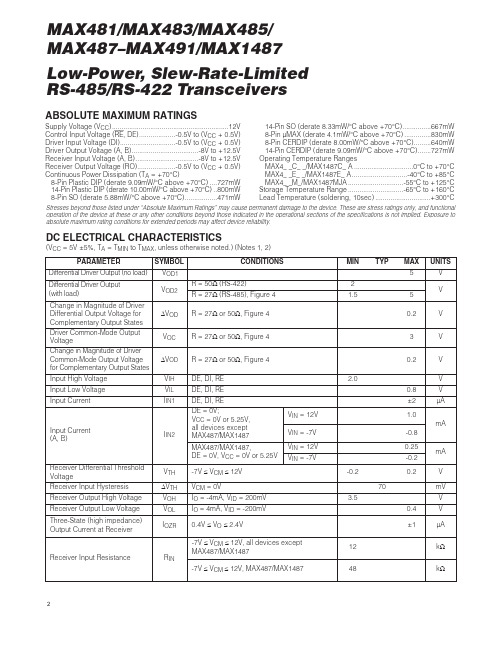
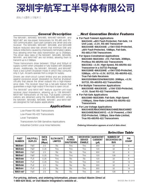
Low-Power, Slew-Rate-Limited RS-485/RS-422 Transceivers2MAX481/MAX483/MAX485/MAX487–MAX491/MAX1487ABSOLUTE MAXIMUM RATINGSSupply Voltage (V CC ) (12V)Control Input Voltage (RE , DE)...................-0.5V to (V CC + 0.5V)Driver Input Voltage (DI).............................-0.5V to (V CC + 0.5V)Driver Output Voltage (A, B)...................................-8V to +12.5VReceiver Input Voltage (A, B).................................-8V to +12.5VReceiver Output Voltage (RO)....................-0.5V to (V CC + 0.5V)Continuous Power Dissipation (T A = +70°C)8-Pin Plastic DIP (derate 9.09mW/°C above +70°C)....727mW14-Pin Plastic DIP (derate 10.00mW/°C above +70°C)..800mW8-Pin SO (derate 5.88mW/°C above +70°C).................471mW 14-Pin SO (derate 8.33mW/°C above +70°C)...............667mW 8-Pin µMAX (derate 4.1mW/°C above +70°C)..............830mW 8-Pin CERDIP (derate 8.00mW/°C above +70°C).........640mW 14-Pin CERDIP (derate 9.09mW/°C above +70°C).......727mW Operating Temperature Ranges MAX4_ _C_ _/MAX1487C_ A...............................0°C to +70°C MAX4__E_ _/MAX1487E_ A.............................-40°C to +85°C MAX4__M_/MAX1487MJA.............................-55°C to +125°C Storage Temperature Range.............................-65°C to +160°C Lead Temperature (soldering, 10sec).............................+300°C DC ELECTRICAL CHARACTERISTICS(V CC = 5V ±5%, T A = T MIN to T MAX , unless otherwise noted.) (Notes 1, 2)Stresses beyond those listed under “Absolute Maximum Ratings” may cause permanent damage to the device. These are stress ratings only, and functional operation of the device at these or any other conditions beyond those indicated in the operational sections of the specifications is not implied. Exposure to absolute maximum rating conditions for extended periods may affect device reliability.V V IN = -7V V IN = 12V V IN = -7V V IN = 12V Input Current (A, B)I IN2V TH k Ω48-7V ≤V CM ≤12V, MAX487/MAX1487R INReceiver Input Resistance -7V ≤V CM ≤12V, all devices exceptMAX487/MAX1487R = 27Ω(RS-485), Figure 40.4V ≤V O ≤2.4VR = 50Ω(RS-422)I O = 4mA, V ID = -200mV I O = -4mA, V ID = 200mV V CM = 0V -7V ≤V CM ≤12V DE, DI, REDE, DI, RE MAX487/MAX1487,DE = 0V, V CC = 0V or 5.25VDE, DI, RE R = 27Ωor 50Ω, Figure 4R = 27Ωor 50Ω, Figure 4R = 27Ωor 50Ω, Figure 4DE = 0V;V CC = 0V or 5.25V,all devices exceptMAX487/MAX1487CONDITIONS k Ω12µA ±1I OZR Three-State (high impedance)Output Current at Receiver V 0.4V OL Receiver Output Low Voltage3.5V OH Receiver Output High VoltagemV 70ΔV TH Receiver Input HysteresisV -0.20.2Receiver Differential ThresholdVoltage-0.2mA 0.25mA -0.81.01.55V OD2Differential Driver Output(with load)V 2V 5V OD1Differential Driver Output (no load)µA ±2I IN1Input Current V 0.8V IL Input Low VoltageV 2.0V IH Input High VoltageV 0.2ΔV OD Change in Magnitude of DriverCommon-Mode Output Voltagefor Complementary Output StatesV 0.2ΔV OD Change in Magnitude of DriverDifferential Output Voltage forComplementary Output StatesV 3V OC Driver Common-Mode OutputVoltageUNITS MIN TYP MAX SYMBOL PARAMETERLow-Power, Slew-Rate-Limited RS-485/RS-422 Transceivers7MAX481/MAX483/MAX485/MAX487–MAX491/MAX1487______________________________________________________________Pin DescriptionFigure 1. MAX481/MAX483/MAX485/MAX487/MAX1487 Pin Configuration and Typical Operating Circuit。
RECOM 电源调压器 R-5xxxA 系列数据手册说明书

FeaturesSwitching Regulator• Non-isolated• Synchronous rectification design • Adjustable output voltage• 2, 3, 4 & 5AMP adjustable positive step down integrated switching regulator • Over load protection• Continuous short circuit protection • Efficiency up to 96%R-5xxxPA_DADescriptionThe R-5xxxA series is a high performance 1.2V to 5.5V, 2Amp to 5Amp, 12-Pin SIP (single in-line package) integrated switching regulator (ISR). The synchronous - rectified design yields excellent efficiencies up to 96%. Short circuit protection reduces the short circuit input current to under 50mA. Autosense function compensates for any losses in long circuit loops.DC/DC Converter2,3,4,5 Amp SIP12Vertical &IEC/EN60950-1 certifiedR-542.5xA 4.5 - 18 2.5 1.6 - 5.5 4 91 89 88 300/6800R-543.3xA 4.5 - 18 3.3 1.6 - 5.5 4 93 92 91 300/6800R-545.0xA 6.5 - 18 5.0 3.0 - 5.5 4 95 94 93 300/6800R-551.2xA 4.4 - 18 1.2 1.0 - 3.0 5 81 80 78 300/6800R-551.8xA 4.5 - 18 1.8 1.1 - 4.5 5 86 85 84 300/6800R-552.5xA 4.5 - 18 2.5 1.6 - 5.5 5 90 89 88 300/6800R-553.3xA 4.5 - 18 3.3 1.6 - 5.5 5 92 91 90 300/6800R-555.0xA 7.0 - 1.8 5.0 3.0 - 5.5 5 94 93 92 300/6800Notes:Note1: Vin-Vout ≥ 1.5V~4.0V depending on Vout if adjust function is used Note2: please refer to basic characteristicsNotes:Note3: x can be …P“= vertical through hole x can be …D“ = bent for horizontal through hole mountingModel NumberingOrdering Examples:R-553.3PA Iout= 5A nom. Vout= 3.3VDC P= vertical through holeR-522.5DA Iout= 2Anom. Vout= 2.5VDC D= bent for horizontal through hole mountingPinning (3)Output Current (A)nom. Output VoltageR-5_ __ xASpecifications (refer to standard application circuit, Ta= 25°C)Specifications (refer to standard application circuit, Ta= 25°C)Specifications (refer to standard application circuit, Ta= 25°C)Trim Tables or Calculation2ADC R-521.2PA/DA R-521.8PA/DA R-522.5PA/DA R-523.3PA/DA R-525.0PA/DA 3ADC R-531.2PA/DA R-531.8PA/DA R-532.5PA/DA R-533.3PA/DA R-535.0PA/DA 4ADC R-541.2PA/DA R-541.8PA/DA R-542.5PA/DA R-543.3PA/DA R-545.0PA/DA 5ADC R-551.2PA/DA R-551.8PA/DA R-552.5PA/DA R-553.3PA/DA R-555.0PA/DAVout nom. 1.2VDC 1.8VDC 2.5VDC 3.3VDC 5.0VDC Vout adj.R1R2R1R2R1R2R1R2R1R21.337kΩ 3.7kΩ750Ω1.511.5kΩ10kΩ2.1KΩ390Ω1.68.2kΩ18kΩ 3.0KΩ750Ω1.7 6.5kΩ41kΩ 4.1KΩ 1.2kΩ1.8 5.2kΩ 5.6KΩ 1.7kΩ1.9 4.3kΩ36kΩ7.5KΩ2.2kΩ2.03.6kΩ 1.8kΩ10.5KΩ 2.8kΩ2.4 2.1kΩ 5.2kΩ82KΩ 6.8kΩ2.5 1.8kΩ 4.3kΩ8.5kΩ2.6 1.65kΩ3.6kΩ33kΩ10.5kΩ3.0 1.05kΩ 2.1kΩ 6.2kΩ33kΩ470Ω3.2 1.65kΩ4.1kΩ110kΩ 1.6kΩ3.3 1.5kΩ 3.4kΩ 2.2kΩ3.4 1.35kΩ 2.9kΩ36kΩ 3.0kΩ3.6 1.07kΩ 2.2kΩ11kΩ4.7kΩ3.9780Ω 1.4kΩ4.7kΩ8.5kΩ4.5390Ω650Ω 1.6Ω30kΩ4.9350Ω820Ω220kΩ5.0290Ω680Ω5.1220Ω560Ω28kΩ5.539Ω190Ω 2.6kΩSpecifications (refer to standard application circuit, Ta= 25°C)PROTECTIONSParameter Condition Value Short Circuit Protection (SCP)continuous, automatic recovery Short Circuit Input Current50mA max.continued on next pageSpecifications (refer to standard application circuit, Ta= 25°C)DIMENSION AND PHYSICAL CHARACTERISTICSParameterTypeValueMaterial case pottingnon-conducive black plastic, (UL94 V-0)epoxy, (UL94 V-0)Dimension (LxWxH)32.2 x 9.1 x 15.0mmWeight9g typ.continued on next pageENVIRONMENTALParameterConditionValueOperating Temperature Range *************************************/s-40°C to +85°CMaximum Case Temperature +110°C Thermal Impedance @ natural convection 0.1m/s25°C/W Operating Humidity non-condensing95% RH max.Operating Altitude 2000m Pollution Degree PD2MTBFaccording to MIL-HDBK 217F, G.B.+25°C +85°C749 x 103 hours 150 x 103 hoursSAFETY AND CERTIFICATIONSCertificate Type (Safety)Report / File NumberStandard Information Technology Equipment, General Requirements for Safety 1605077-12IEC60950-1:2005, 2nd Edition + AM2:2013EN60950-1:2006 + AM2:2013EAC RU-AT.49.09571TP TC 004/2011RoHS 2+RoHS-2011/65/EU + AM-2015/863Specifications (refer to standard application circuit, Ta= 25°C)PACKAGING INFORMATIONParameter Type ValuePackaging Dimensions (LxWxH)R-5xxxDAR-5xxxPA520.0 x 20.0 x 19.0mm530.0 x 23.0 x 19.0mmPackaging Quantity tube 15pcs Storage Temperature Range-40°C to +125°CThe product information and specifications may be subject to changes even without prior written notice.The product has been designed for various applications; its suitability lies in the responsibility of each customer. The products are not authorized for use in safety-critical applications without RECOM’s explicit written consent. A safety-critical application is an application where a failure may reasonably be expected to endanger or cause loss of life, inflict bodily harm or damage property. The applicant shall indemnify and hold harmless RECOM, its affiliated companies and its representatives against any damage claims in connection with the unauthorizeduse of RECOM products in such safety-critical applications.。
HPMLDL系列服务器

HPMLDL系列服务器hpML系列服务器HP ProLiant ML110G7(C8R00A)参数规格差不多参数产品类型工作组级产品类别塔式产品结构4U处理器CPU类型奔腾双核CPU型号奔腾双核G860CPU频率3GHzHP ProLiant ML330 G6(600911-AA1)参数规格差不多参数产品类型企业级产品类别塔式产品结构5U处理器CPU类型Intel 至强5600CPU型号Xeon E5620CPU频率 2.4GHz智能加速主2.666GHz频标配CPU1颗数量最大CPU2颗数量制程工艺32nm三级缓存12MB总线规格QPI 5.86GT/sCPU核心四核HP ProLiant ML330 G6(B9D22A)参数规格差不多参数产品类型企业级产品类别塔式产品结构5U处理器CPU类型Intel 至强5600 CPU型号Xeon E5606CPU频率 2.13GHz标配CPU1颗数量最大CPU2颗数量制程工艺32nm三级缓存8MB总线规格QPI 4.8GT/sHP ProLiant ML330 G6(600911-AA1)参数规格差不多参数产品类型企业级产品类别塔式产品结构5U处理器CPU类型Intel 至强5600CPU型号Xeon E5620CPU频率 2.4GHz智能加速主2.666GHz频标配CPU1颗数量最大CPU2颗数量制程工艺32nm三级缓存12MB总线规格QPI 5.86GT/sCPU核心四核HP ProLiant ML350 G6(638180-AA1)参数规格差不多参数产品类别塔式产品结构5U处理器CPU类型Intel 至强5600CPU型号Xeon E5606CPU频率 2.13GHz标配CPU1颗数量最大CPU2颗数量制程工艺32nm三级缓存8MB总线规格QPI 4.8GT/sCPU核心四核CPU线程四线程数主板HP ProLiant ML350 G6(600431-AA5)参数规格差不多参数产品类别塔式产品结构5U处理器CPU类型Intel 至强5600CPU型号Xeon E5620CPU频率 2.4GHz智能加速主2.666GHz频标配CPU1颗数量最大CPU2颗数量制程工艺32nm三级缓存12MB总线规格QPI 5.86GT/sCPU核心四核CPU线程八线程数HP ProLiant ML350 G6(594869-AA1)参数规格差不多参数产品类别塔式产品结构5U处理器CPU类型Intel 至强5600CPU型号Xeon E5620CPU频率 2.4GHz智能加速主2.666GHz频标配CPU1颗数量最大CPU2颗数量制程工艺32nm三级缓存12MB总线规格QPI 5.86GT/sCPU核心四核CPU线程八线程数HP ProLiant ML310e Gen8(686146-AA5)参数规格差不多参数产品类型企业级产品类别塔式产品结构4U处理器CPU类型Intel 至强E3-1200 v2 CPU型号Xeon E3-1220 v2CPU频率 3.1GHz标配CPU1颗数量最大CPU4颗数量制程工艺22nm三级缓存8MB总线规格DMI 5GT/sHP ProLiant ML310e Gen8(686147-AA5)参数规格差不多参数产品类型企业级产品类别塔式产品结构4U处理器CPU类型Intel 至强E3-1200 v2 CPU型号Xeon E3-1240 v2CPU频率 3.4GHz智能加速主3.8GHz频标配CPU1颗数量最大CPU4颗数量制程工艺22nm三级缓存8MBHP ProLiant ML350e Gen8(C3Q10A)参数规格差不多参数产品类型企业级产品类别塔式产品结构5U处理器CPU类型Intel 至强E5-2400 CPU型号Xeon E5-2403CPU频率 1.8GHz标配CPU1颗数量最大CPU4颗数量制程工艺32nm三级缓存10MB总线规格QPI 6.4GT/sHP ProLiant ML350e Gen8(C3Q08A)参数规格差不多参数产品类型企业级产品类别塔式产品结构5U处理器CPU类型Intel 至强E5-2400 CPU型号Xeon E5-2407CPU频率 2.2GHz标配CPU1颗数量最大CPU4颗数量制程工艺32nm三级缓存10MB总线规格QPI 6.4GT/sHP ProLiant ML350e Gen8(C3Q09A)参数规格差不多参数产品类型企业级产品类别塔式产品结构5U处理器CPU类型Intel 至强E5-2400 CPU型号Xeon E5-2420CPU频率 1.9GHz标配CPU1颗数量最大CPU4颗数量制程工艺32nm三级缓存15MB总线规格QPI 6.4GT/sHP ProLiant ML350e Gen8(C3F91A)参数规格差不多参数产品类型企业级产品类别塔式产品结构5U处理器CPU类型Intel 至强E5-2400 CPU型号Xeon E5-2430CPU频率 2.2GHz标配CPU1颗数量最大CPU4颗数量制程工艺32nm三级缓存15MB总线规格QPI 6.4GT/sHP ProLiant ML350p Gen8(646675-AA1)参数规格差不多参数产品类别塔式产品结构5U处理器CPU类型Intel 至强E5-2600 CPU型号Xeon E5-2609CPU频率 2.4GHz标配CPU1颗数量最大CPU2颗数量制程工艺32nm三级缓存10MB总线规格QPI 6.4GT/sHP ProLiant ML350p Gen8(668271-AA5)参数规格差不多参数产品类别塔式产品结构5U处理器CPU类型Intel 至强E5-2600 CPU型号Xeon E5-2620CPU频率2GHz智能加速主2.5GHz频标配CPU1颗数量最大CPU2颗数量制程工艺32nm。
飞利浦 DVD播放机 说明书

48目錄語言代碼----------------------------------------------5介紹提供配件--------------------------------------------50清潔光碟--------------------------------------------50設置--------------------------------------------------50連接連接電視機-------------------------------------51-52使用複合視頻插孔(CVBS)...................51使用色差視頻插孔(Y Pb Pr).................51使用RF 調制器配件................................52連接電源線------------------------------------------52選項:連接至多通道接收器---------------------53A/V 功放具有杜比數碼或DTS 解碼功能....................................................................53選項: 連接立體聲系統----------------------------53立體聲有杜比環繞立體聲或左/右Audio In 的插孔....................................................53選項: 連接數碼AV 接收器----------------------54接收器有一個PCM 、杜比數碼 或MPEG 解碼器....................................................54選項:連接至HDMI 的插孔---------------------55使用HDMI(高解析度多媒體介面)插座..............................................................55選項:連接至一個可支持的USB 設備-------56使用USB 插口........................................56功能概覽前后面板--------------------------------------------57遙控器-----------------------------------------------58啟動步驟一:在遙控器裝入電池---------------------59使用遙控器操作本音響系統....................59步驟二:設定電視機-------------------------59-61設定逐行掃描功能(只適用於有逐行掃描電視機)..................................................60選擇對應電視機的制式...........................61步驟三:設置界面語言--------------------------62設定屏幕顯示語言..................................62設定聲音、字幕和碟片菜單語言. (62)光碟操作適合播放的媒體類別-----------------------------63地區編碼--------------------------------------------63播放光碟--------------------------------------------64基本播放控制---------------------------------------64影像播放操作方式(DVD/VCD/SVCD)-----65使用光碟目錄.........................................65放大........................................................65由最后停止的點,恢復播放....................65慢放........................................................65向前∕向后搜索......................................65OSD (在屏幕顯示) (DVD/VCD/SVCD)---66-68使用OSD 選單.......................................66選擇標題∕章節∕曲目...........................66時間搜索.................................................66聲音∕字幕.............................................67角度........................................................67瀏覽功能.................................................67重複播放模式.........................................68個章節∕曲目重複一個段落....................68OSD (在屏幕顯示) (Audio CD)-----------------68盤片時間∕曲目時間∕選擇曲目.............68重複........................................................68DVD 的特殊功能-----------------------------------69標題播放.................................................69改變聲音語言.........................................69多字幕功能.............................................69VCD 與SVCD 的特殊功能----------------------69對於播放控制(PBC).............................69播放DivX 光碟-------------------------------------70從支持的USB 設備播放圖片或音頻文件----71USB 設備的兼容性.................................71播放MP3/WMA/JPEG/Kodak 影像光碟-72-73基本操作.................................................72播放選擇.................................................72瀏覽功能(JPEG)..................................72圖像放大功能(JPEG)...........................73多角度效果播放功能(JPEG)................73同時播放MP3/WMA 音樂與JPEG 影像................................................................73卡拉OK 操作卡拉OK 光碟的播放------------------------------74基本操作.................................................74伴唱........................................................74卡拉OK..................................................74DVP5965K_93_CS(0608)212/21/06, 2:35 PM4849DVD 設定選單項目通用設定頁-------------------------------------75-76光碟收看鎖碼∕取消光碟收看鎖碼.........75降低機器顯示面板的亮度.......................75編程光碟曲目(不適用於CD/MP3/WMA/DivX).................................................75-76OSD 語言...............................................76睡眠........................................................76DivX(R) VOD 注冊碼..............................76音頻設定頁-------------------------------------77-79模擬輸出.................................................77數字音頻設定.........................................77聲音模式.................................................78揚聲器設定.............................................78CD 升頻..................................................78夜間模式啟動∕關閉...............................79視頻設定頁-------------------------------------79-82電視機制式.............................................79屏幕畫面比例.........................................80逐行掃描啟動∕關閉...............................80畫質設定.................................................81高解析度JPEG 影像模式.......................82HDMI 設定..............................................82初期設定頁-------------------------------------82-84聲音、字幕、碟片菜單語言....................82透過設定年齡控制播放...........................83PBC........................................................83MP3/JPEG 選單啟動∕關閉...................83變更密碼.................................................84設置DivX 字幕........................................84恢復原廠設定.........................................84聲音和音量控制設定揚聲器的聲道--------------------------------85故障指南---------------------------------------86-87產品規格--------------------------------------------88詞匯--------------------------------------------------89目錄DVP5965K_93_CS(0608)212/21/06, 2:35 PM4950提供配件複合視頻接線(黃色)音頻接線(白色、紅色)遙控器和兩枚電池介紹清潔光碟如要清潔光碟,使用具有微纖維的清潔軟布,由光碟的中心以直線方向抹至碟邊。
MEMORY存储芯片MAX490EESA+T中文规格书

Cs 100pF
STORAGE CAPACITOR
Figure 4. Human Body ESD Test Model
RC 50M to 100M RD 330Ω
CHARGE CURRENT LIMIT RESISTOR
DISCHARGE RESISTANCE
HIGHVOLTAGE
4
3
5
DI
put Z high. Similarly, a high on DI forces output Y high
and output Z low.
5
4
6, 7
GND
Ground
—
5
9
Y
Noninverting Driver Output
—
6
10
Z
Inverting Driver Output
______________________________________________________________Pin Description
PIN
MAX481E/MAX483E MAX485E/MAX487E
MAX1487E
MAX488E MAX490E
MAX489E MAX491E
NAME
TIME
tDL CURRENT WAVEFORM
Figure 5. Human Body Model Current Waveform
I 100% 90%
IPEAK
DEVICE UNDER TEST
10%
tr = 0.7ns to 1ns
t
30ns
60ns
Figure 7. IEC1000-4-2 ESD Generator Current Waveform
MIC4802YME;中文规格书,Datasheet资料

January 2011
M9999-013111-B
/
Micrel Inc.
Ordering Information
Part Number MIC4802YME
Pin Configuration
Temperature Range –40°C to +125°C
MIC4802
MIC4802
High Efficiency 800mA Single Channel Linear WLED Driver with Ultra Fast PWM™ Control
General Description
The MIC4802 is a high efficiency White LED (WLED) driver designed to drive a single LED up to 800mA. The MIC4802 constant current driver is designed to drive high power LED’s in various lighting applications. The MIC4802 provides the highest possible efficiency as this architecture has no switching losses present in traditional charge pumps or inductive boost circuits. It features a typical dropout of 280mV at 800mA. This allows the LEDs to be driven directly from the voltage source eliminating switching noise/losses present with the use of boost circuitry. The high accuracy (±1% Typical) current regulated WLED channel ensures uniform display illumination under all conditions. The brightness is controlled through an Ultra Fast PWM™ Control interface operating down to less than 1% duty cycle.
三汇 NTP-480A PCIe(2.0) VoIP 录音卡 用户手册说明书
三汇NTP系列录音卡NTP-480A/PCIe(2.0)VoIP录音卡Version 1.0杭州三汇信息工程有限公司目录目录 (i)版权申明 (ii)版本修订记录 (iii)第1章概述 (1)1.1功能描述 (1)1.2性能特点 (1)第2章安装 (3)2.1结构示意图 (3)2.2系统要求 (5)2.3安装步骤 (5)附录A 主要技术/性能参数 (6)附录B 技术/销售支持 (7)版权申明本文档版权属杭州三汇信息工程有限公司所有。
杭州三汇信息工程有限公司保留对此文件进行修改而不另行通知之权利。
杭州三汇信息工程有限公司承诺所提供的信息为正确且可靠, 但并不保证本文件绝无错误。
请在使用本产品前, 自行确定所使用的相关技术文件及规格为最新有效之版本。
若因贵公司使用本公司之文件或产品, 而需要第三方之产品、专利或者著作等与其配合时,则应由贵公司负责取得第三方同意及授权。
关于上述同意及授权,非属本公司应为保证之责任。
版本修订记录版本号发布日期修订内容Version1.0 2017.07 新创建此文档。
请访问我们的网站()以获取该文档的最新版本。
第1章 概述NTP系列NTP-480A/PCIe(2.0) VoIP录音卡是三汇公司推出的最大可支持480路IP通话录音的板卡。
本系列板卡可以应用于100M/1000M的网络环境,可通过交换机端口镜像录音。
1.1 功能描述●单卡提供最多480路IP电话处理能力。
●通过端口镜像实现目标交换机的数据采集,能够支持两台交换机同时录音。
●板卡采用端口镜像的形式采集网络上的语音数据,并转发到PC机上。
不对原有通话双方造成任何干扰,也不会被通话双方察觉。
●固件中均写入了唯一的硬件序列号,可用于区分板卡类型,亦可作防伪识别。
●具有硬件授权号识别电路。
用户可向本公司申请唯一的授权号,保护用户软件安全。
1.2 性能特点●支持PCIe x1总线PCIe x1接口,符合PCIe1.0a总线标准,适用各种PCIe插槽,支持即插即用(PNP)。
海哥尔德电子产品简介说明书

APRIL 2013Quick-Refere nce GuideLAPTOP, DESKTO P AND VIDEO STORAGE DRIVESSeagate Partner Program MembersVisit the Sales Tools section to access the latestproduct roadmap, end-of-life schedule and product information. DistributorsEMEA SPP Support00-800-6890-8282US Sales Support1-800-SEAGATE or 1-405-324-4700Visit for more information or call 1-800-SEAGATE (1-800-732-4283) © 2013 Seagate Technology LLC. All rights reserved. Printed in USA. Seagate, Seagate Technology and the Wave logo are registered trademarks of Seagate Technology LLC in the United States and/or other countries. Barracuda, G-Force Protection, Momentus, Pipeline HD, SmartAlign and SV35 Series are either trademarks or registered trademarks of Seagate Technology LLC or one of its affiliated companies in the United States and/or other countries. The FIPS logo is a certification mark of NIST, which does not imply product endorsement by NIST, the U.S., or Canadian governments. All other trademarks or registered trademarks are the property of their respective owners. When referring to drive capacity, one gigabyte, or GB, equals one billion bytes and one terabyte, or TB, equals one trillion bytes. Your computer’s operating system may use a different standard of measurement and report a lower capacity. In addition, some of the listed capacity is used for formatting and other functions, and thus will not be available for data storage. Actual data rates may vary depending on operating environment and other factors. The export or re-export of hardware or software containing encryption may be regulated by the US Department of Commerce, Bureau of Industry and Security (for more information go to ). Seagate reserves the right to change, without notice, product offerings or specifications. QR502.15-1304GB, April 2013APRIL 2013Quick-Reference GuideLAPTOP, DESKTOP AND VIDEO STORAGE DRIVESNew Seagate Model Number KeyDesktop, laptop and video storageST 500 DX 001BRANdCAPACiTySegMeNTATTRiBuTeS2 letters ST= Seagate MX= Maxtor2 to 4 digits 80 = 80GB 500 = 500GB 1500 = 1,500GB Capacities>9,999GB: 10 = 10TB 15 = 15TB2 lettersDX = Desktop Premium DM = Mainstream DL = Entry LevelLX = Laptop Premium LM = Laptop Mainstream LT = Laptop Thin VX = Surveillance VM = DVR VT = DVR Thin3 digits, non-intelligent Varies for:Z-height Form Factor RPM Cache Interface SED, FIPS Drop Sensor Interface SpeedView a brief training presentation on how our model numbering format has changed at /seagate/ModelNumber 1 One gigabyte, or GB, equals one billion bytes; and one terabyte, or TB, equals one trillion bytes when referring to drive capacity.2See FIPS 140-2 Level 2 Certificate at /groups/STM/cmvp/documents/140-1/1401vend.htm.37mm z-height expanded to 9.5mm enables compatibility with standard laptop chassis.4Advanced Format 4K sector drive with SmartAlign ™ technology resolves misalignment conditions.5Seagate makes this drive in both 4K and 512-byte sectors. SmartAlign technology is included on 4K sector drives. Both drives are functionally and physically equivalent.6Formerly Barracuda ®drive。
ADM3251E中文资料
ADM3251E中⽂资料Isolated, Single-ChannelRS-232 Line Driver/ReceiverADM3251E Rev. AInformation furnished by Analog Devices is believed to be accurate and reliable. However, noresponsibility is assumed by Analog Devices for its use, nor for any infringements of patents or other rights of third parties that may result from its use. Specifications subject to change without notice. No license is granted by implication or otherwise under any patent or patent rights of Analog Devices. T rademarks and registered trademarks are the property of their respective owners. One Technology Way, P.O. Box 9106, Norwood, MA 02062-9106, U.S.A. Tel: 781.329.4700/doc/5553137527284b73f2425087.html Fax: 781.461.3113 ?2008 Analog Devices, Inc. All rights reserved.FEATURES2.5 kV fully isolated (power and data) RS-232 transceiver iso Power integrated, isolated dc-to-dc converter460 kbps data rate1 Tx and 1 RxMeets EIA/TIA-232E specificationsESD protection on R IN and T OUT pins±8 kV: contact discharge±15 kV: air gap discharge0.1 µF charge pump capacitorsHigh common-mode transient immunity: >25 kV/µs Safety and regulatory approvals (pending)UL recognition2500 V rms for 1 minute per UL 1577VDE Certificate of ConformityDIN V VDE V 0884-10 (VDE V 0884-10):2006-12V IORM = 560 V peakOperating temperature range: ?40°C to +85°CWide body, 20-lead SOIC packageAPPLICATIONSHigh noise data communicationsIndustrial communicationsGeneral-purpose RS-232 data linksIndustrial/telecommunications diagnostic ports Medical equipmentFUNCTIONAL BLOCK DIAGRAM78-1C40.1µF* *5k? PULL-DOWN RESISTOR ON THE RS-232 INPUT.C30.1µFC20.1µFC10.1µFFigure 1.GENERAL DESCRIPTIONThe ADM3251E is a high speed, 2.5 kV fully isolated, single-channel RS-232/V.28 transceiver device that operates from a single 5 V power supply. Due to the high ESD protection on the R IN and T OUT pins, the device is ideally suited for operation in electrically harsh environments or where RS-232 cables are frequently being plugged and unplugged.The ADM3251E incorporates dual-channel digital isolators with iso Power? integrated, isolated power. There is no requirement to use a separate isolated dc-to-dc converter. Chip-scale trans-former i Coupler? technology from Analog Devices, Inc., is used both for the isolation of the logic signals as well as for the integrated dc-to-dc converter. The result is a total isolation solution. The ADM3251E conforms to the EIA/TIA-232E and ITU-T V. 28 specifications and operates at data rates up to 460 kbps.Four external 0.1 µF charge pump capacitors are used for the voltage doubler/inverter, permitting operation from a single5 V supply.The ADM3251E is available in a 20-lead, wide body SOIC package and is specified over the ?40°C to +85°C temperature range.ADM3251ERev. A | Page 2 of 16TABLE OF CONTENTSFeatures .............................................................................................. 1 Applications ....................................................................................... 1 Functional Block Diagram .............................................................. 1 General Description ......................................................................... 1 Revision History . (2)Specifications ..................................................................................... 3 Package Characteristics ............................................................... 5 Regulatory Information (Pending) ............................................ 5 Insulation and Safety-Related Specifications ............................ 5 DIN V VDE V 0884-10 (VDE V 0884-10):2006-12 InsulationCharacteristics (Pending) ............................................................ 6 Absolute Maximum Ratings ............................................................7 ESD Caution .................................................................................. 7 Pin Configuration and Function Descriptions ..............................8 Typical Performance Characteristics ..............................................9 Theory of Operation ...................................................................... 11 Isolation of Power and Data ...................................................... 11 Charge Pump Voltage Converter ............................................. 12 5.0 V Logic to EIA/TIA-232E Transmitter .............................. 12 EIA/TIA-232E14 Ordering Guide .. (14)REVISION HISTORY9/08—Rev. 0 to Rev. AChanges to Timing Parameters in Table 1 ..................................... 3 Changes to Timing Parameters in Table 2 ..................................... 4 Changes to Ordering Guide .......................................................... 14 7/08—Revision 0: Initial VersionADM3251ERev. A | Page 3 of 16SPECIFICATIONSAll voltages are relative to their respective ground; all minimum/maximum specifications apply over the entire recommended operating range; T A = 25°C and V CC = 5.0 V (dc-to-dc converter enabled), unless otherwise noted. Table 1.Parameter Min Typ Max Unit Test Conditions/Comments DC CHARACTERISTICS V CC Operating Voltage Range 4.5 5.5 VDC-to-DC Converter Enable Threshold, V CC(ENABLE)14.5 VDC-to-DC Converter Disable Threshold, V CC(DISABLE)1 3.7 V DC-to-DC Converter EnabledInput Supply Current, I CC(ENABLE) 110 mA V CC = 5.5 V, no load 145 mA V CC = 5.5 V, R L = 3 kΩV ISO Output 25.0 V I ISO = 0 µA LOGIC Transmitter Input, T IN Logic Input Current, I TIN ?10 +0.01 +10 µA Logic Low Input Threshold, V TINL 0.3 V CC V Logic High Input Threshold, V TINH 0.7 V CC V Receiver Output, R OUT Logic High Output, V ROUTH V CC ? 0.1 V CC V I ROUTH = ?20 µA V CC ? 0.5 V CC ? 0.3 V I ROUTH = ?4 mA Logic Low Output, V ROUTL 0.0 0.1 V I ROUTH = 20 µA0.3 0.4 V I ROUTH = 4 mA RS-232 Receiver, R INEIA-232 Input Voltage Range 330 +30 V EIA-232 Input Threshold Low 0.6 2.0 V EIA-232 Input Threshold High 2.1 2.4 V EIA-232 Input Hysteresis 0.1 V EIA-232 Input Resistance 3 5 7 kΩ Transmitter, T OUT Output Voltage Swing (RS-232) ±5 ±5.7 V R L = 3 kΩ to GND Transmitter Output Resistance 300 Ω V ISO = 0 V Output Short-Circuit Current (RS-232) ±12 mA TIMING CHARACTERISTICS Maximum Data Rate 460 kbps R L = 3 kΩ to 7 kΩ, C L = 50 pF to 1000 pF Receiver Propagation Delayt PHL 190 ns t PLH 135 ns Transmitter Propagation Delay 650 ns R L = 3 kΩ, C L = 1000 pF Transmitter Skew 80 ns Receiver Skew 70 nsTransition Region Slew Rate3 5.5 10 30 V/µs +3 V to ?3 V or ?3 V to +3 V, V CC = +3.3 V, R L = +3 kΩ, C L = 1000 pF, T A = 25°CAC SPECIFICATIONS Output Rise/Fall Time, t R /t F (10% to 90%) 2.3 ns C L = 15 pF, CMOS signal levelsCommon-Mode Transient Immunity at Logic High Output 425 kV/µs V CM = 1 kV, transient magnitude = 800 VCommon-Mode Transient Immunity at Logic Low Output425 kV/µs V CM = 1 kV, transient magnitude = 800 V ESD PROTECTION (R IN And T OUT PINS)±15 kV Human body model air discharge ±8 kV Human body model contact dischargeTo maintain data sheet specifications, do not draw current from V ISO . 3Guaranteed by design. 4CM is the maximum common-mode voltage slew rate that can be sustained while maintaining specification-compliant operation. V CM is the common-mode potential difference between the logic and bus sides. The transient magnitude is the range over which the common mode is slewed. The common-mode voltage slew rates apply to both rising and falling common-mode voltage edges.ADM3251ERev. A | Page 4 of 16All voltages are relative to their respective ground; all minimum/maximum specifications apply over the entire recommended operating range; T A = 25°C, V CC = 3.3 V (dc-to-dc converter disabled), and the secondary side is powered externally by V ISO = 3.3 V , unless otherwise noted. Table 2.Parameter Min Typ Max Unit Test Conditions/Comments DC CHARACTERISTICS V CC Operating Voltage Range 3.0 3.7 VDC-to-DC Converter Disable Threshold, V CC(DISABLE)13.7 V DC-to-DC Converter DisabledV ISO 2 3.0 5.5 V Primary Side Supply Input Current, I CC(DISABLE) 1.5 mA No load Secondary Side Supply Input Current, I ISO(DISABLE) 12 mA V ISO = 5.5 V, R L = 3 kΩ Secondary Side Supply Input Current, I ISO(DISABLE) 6.2 mA R L = 3 kΩLOGIC Transmitter Input, T IN Logic Input Current, I TIN ?10 +0.01 +10 µA Logic Low Input Threshold, V TINL 0.3 V CC V Logic High Input Threshold, V TINH 0.7 V CC V Receiver Output, R OUT Logic High Output, V ROUTH V CC ? 0.1 V CC V I ROUTH = ?20 µA V CC ? 0.5 V CC ? 0.3 V I ROUTH = ?4 mA Logic Low Output, V ROUTL 0.0 0.1 V I ROUTH = 20 µA 0.3 0.4 V I ROUTH = 4 mA RS-232 Receiver, R INEIA-232 Input Voltage Range 330 +30 V EIA-232 Input Threshold Low 0.6 1.3 VEIA-232 Input Threshold High 1.6 2.4 VEIA-232 Input Hysteresis 0.3 V EIA-232 Input Resistance 3 5 7 kΩ Transmitter, T OUT Output Voltage Swing (RS-232) ±5±5.7 V R L = 3 kΩ to GND Transmitter Output Resistance 300 Ω V ISO = 0 V Output Short-Circuit Current (RS-232) ±11 mA TIMING CHARACTERISTICS Maximum Data Rate 460 kbps R L = 3 kΩ to 7 kΩ, C L = 50 pF to 1000 pF Receiver Propagation Delayt PHL 190 ns t PLH 135 ns Transmitter Propagation Delay 650 ns R L = 3 kΩ, C L = 1000 pF Transmitter Skew 80 ns Receiver Skew 55 nsTransition Region Slew Rate3 5.5 10 30 V/µs +3 V to ?3 V or ?3 V to +3 V, V CC = 3.3 V, R L = 3 kΩ, C L = 1000 pF, T A = 25°CAC SPECIFICATIONS Output Rise/Fall Time, t R /t F (10% to 90%) 2.3 ns C L = 15 pF, CMOS signal levelsCommon-Mode Transient Immunity at Logic High Output 425 kV/µs V CM = 1 kV, transient magnitude = 800 VCommon-Mode Transient Immunity at Logic Low Output 425 kV/µs V CM = 1 kV, transient magnitude = 800 V ESD PROTECTION (R IN AND T OUT PINS) ±15 kV Human body model air discharge ±8 kV Human body model contact discharge1 Enable/disable threshold is the V CC voltage at which the internal dc-to-dc converter is enabled/disabled. 2To maintain data sheet specifications, do not draw current from V ISO . 3Guaranteed by design. 4range over which the common mode is slewed. The common-mode voltage slew rates apply to both rising and falling common-mode voltage edges.ADM3251ERev. A | Page 5 of 16PACKAGE CHARACTERISTICSTable 3.ParameterSymbol Min Typ Max Unit Test Conditions Resistance (Input-Output) R I-O 1012 Ω Capacitance (Input-Output) C I-O 2.2 pF f = 1 MHz Input CapacitanceC I 4.0 pF IC Junction-to-Air Thermal ResistanceθJA 47.05 °C/WREGULATORY INFORMATION (PENDING)Table 4.UL 1VDE1577 Component Recognition Program (Pending) Single/Basic Insulation, 2500 V rms Isolation RatingTo be certified according to DIN V VDE V 0884-10 (VDE V 0884-10):2006-122 Reinforced insulation, 560 V peak1 In accordance with UL 1577, each ADM3251E is proof-tested by applying an insulation test voltage ≥3000 V rms for 1 sec (current leakage detection limit = 5 µA). 2In accordance with DIN V VDE V 0884-10, each ADM3251E is proof-tested by applying an insulation test voltage ≥1050 V peak for 1 sec (partial discharge detection limit = 5 pC).INSULATION AND SAFETY-RELATED SPECIFICATIONSTable 5.ParameterSymbol Value Unit ConditionsRated Dielectric Insulation Voltage2500 V rms 1 minute durationMinimum External Air Gap (Clearance) L(I01) 7.7 mm Measured from input terminals to output terminals, shortest distance through airMinimum External Tracking (Creepage)L(I02) 4.16 mm Measured from input terminals to output terminals, shortest distance path along body Minimum Internal Gap (Internal Clearance)0.017 mm Distance through insulation Tracking Resistance (Comparative Tracking Index) CTI >175 V DIN IEC 112/VDE 0303 Part 1Isolation GroupIIIaMaterial group (DIN VDE 0110, 1/89, Table 1)V IORM425V peakContinuous peak voltage across the isolation barrierADM3251ERev. A | Page 6 of 16DIN V VDE V 0884-10 (VDE V 0884-10):2006-12 INSULATION CHARACTERISTICS (PENDING)This isolator is suitable for reinforced isolation only within the safety limit data. Maintenance of the safety data is ensured by protective circuits. Table 6.Description Conditions Symbol Characteristic Unit Installation Classification per DIN VDE 0110 For Rated Mains Voltage ≤150 V rms I to IV For Rated Mains Voltage ≤ 300 V rms I to III Climatic Classification 40/105/21 Pollution Degree (DIN VDE 0110, Table 1) 2 Maximum Working Insulation Voltage V IORM 424 V peak Input-to-Output Test Voltage Method b1 V IORM × 1.875 = V PR , 100% productiontest, t m = 1 sec, partial discharge < 5 pCV PR 795 V peak Method aAfter Environmental Test Subgroup 1 V IORM × 1.6 = V PR , t m = 60 sec, partialdischarge < 5 pCV PR 680 V peak After Input and/or Safety Subgroup 2/Subgroup 3 V IORM × 1.2 = V PR , t m = 60 sec, partialdischarge < 5 pCV P 510 V peak Highest Allowable Overvoltage Transient overvoltage, t TR = 10 sec V TR 4000 V peak Safety-Limiting Values Maximum value allowed in the eventof a failureCase Temperature T S 150 °C Supply Current I S1 531 mA Insulation Resistance at T S V IO = 500 V R S >109 ΩADM3251ERev. A | Page 7 of 16ABSOLUTE MAXIMUM RATINGSTable 7.Parameter RatingV CC , V ISO ?0.3 V to +6 VV+ (V CC ? 0.3 V) to +13 VV? –13 V to +0.3 VInput VoltagesT IN ?0.3 V to (V CC + 0.3 V) R IN ±30 VOutput VoltagesT OUT ±15 V R OUT ?0.3 V to (V CC + 0.3 V) Short-Circuit DurationT OUT ContinuousθJA , Thermal Impedance 47.05°C/WOperating Temperature RangeIndustrial ?40°C to +85°C Storage Temperature Range ?65°C to +150°C Pb-Free Temperature (Soldering, 30 sec) 260°C Stresses above those listed under Absolute Maximum Ratingsmay cause permanent damage to the device. This is a stress rating only; functional operation of the device at these or any other conditions above those indicated in the operational section of this specification is not implied. Exposure to absolute maximum rating conditions for extended periods may affect device reliability. ESD CAUTIONADM3251ERev. A | Page 8 of 16PIN CONFIGURATION AND FUNCTION DESCRIPTIONSNC 1V CC 2V CC 3GND 4V ISO 20V+19C1+18C1–17GND 5T OUT 16GND 6R IN 15GND 7C2+14R OUT 8C2–13T IN 9V–12GND 10GND ISO11NC = NO CONNECTADM3251ETOP VIEW (Not to Scale)07388-002Figure 2. Pin ConfigurationTable 8. Pin Function DescriptionsPin No. Mnemonic Description1 NC No Connect. This pin should always remain unconnected.2, 3V CCPower Supply Input. A 0.1 µF decoupling capacitor is required between V CC and ground. When a voltagebetween 4.5 V and 5.5 V is applied to the V CC pin, the integrated dc-to-dc converter is enabled. If this voltage is lowered to between 3.0 V and 3.7 V, the integrated dc-to-dc converter is disabled. 4, 5, 6, 7, 10 GND Ground Pin.8 R OUT Receiver Output. This pin outputs CMOS logic levels.9 T IN Transmitter (Driver) Input. This pin accepts TTL/CMOS levels. 11 GND ISO Ground Reference for Isolator Primary Side. 12 V? Internally Generated Negative Supply.13, 14 C2?, C2+ Positive and Negative Connections for Charge Pump Capacitors. External Capacitor C2 is connected between these pins; a 0.1 µF capacitor is recommended, but larger capacitors up to 10 µF can be used. 15 R IN Receiver Input. This input accepts RS-232 signal levels.16 T OUT Transmitter (Driver) Output. This outputs RS-232 signal levels.17, 18 C1?, C1+ Positive and Negative Connections for Charge Pump Capacitors. External Capacitor C1 is connected between these pins; a 0.1 µF capacitor is recommended, but larger capacitors up to 10 µF can be used. 19 V+ InternallyIsolated Supply Voltage for Isolator Secondary Side. A 0.1 µF decoupling capacitor is required between V ISO and ground. When the integrated dc-to-dc converter is enabled, the V ISO pin should not be used to power external circuitry. If the integrated dc-to-dc converter is disabled, power the secondary side by applying a voltage in the range of 3.0 V to 5.5 V to this pin.ADM3251ERev. A | Page 9 of 16TYPICAL PERFORMANCE CHARACTERISTICS2004006008001000LOAD CAPACITANCE (pF)T x O U T P U T (V )07388-004Figure 3. Transmitter Output Voltage High/Low vs. LoadCapacitance @ 460 kbps4.54.74.95.1 5.3 5.5V CC (V)T x O U T P U T (V )07388-005Figure 4. Transmitter Output Voltage High/Low vs. V CC , R L = 3 kΩ3.03.54.04.55.0 5.507388-009Figure 5. Transmitter Output Voltage High/Low vs. V ISO , R L = 3 kΩ1234LOAD CURRENT (mA)T x O U T P U T (V )07388-006Figure 6. Transmitter Output Voltage High/Low vs. Load Current1510–5–10–15123LOAD CURRENT (mA)V +, V – (V )07388-0074Figure 7. Charge Pump V+, V? vs. Load Current4003503002502001501005004.504.755.00 5.25 5.50V CC (V)C H A R G E P U M P I M P ED A N CE (?)07388-008Figure 8. Charge Pump Impedance vs. V CCRev. A | Page 10 of 164003503002502001501003.003.25 3.50 3.754.004.25 4.50 4.755.00 5.25 5.50V ISO (V)C H A R G E P U M P I M P ED A N CE (?)07388-010Figure 9. Charge Pump Impedance vs. V ISO 200180160140120100806040204692138184230276322368414460DATA RATE (kbps)S U P P L Y C U R R E N T (m A )07388-003Figure 10. Primary Supply Current vs. Data Rate 073 TIME (500ns/DIV)V CC =5VFigure 11. 460 kpbs Data Transmission4.504.755.00 5.25 5.50T I N V O L T A G E T H R E S H O L D (V )07388-011Figure 12. T IN Voltage Threshold vs. V CCADM3251ERev. A | Page 11 of 16THEORY OF OPERATIONThe ADM3251E is a high speed, 2.5 kV fully isolated, single-channel RS-232 transceiver device that operates from a single power supply.The internal circuitry consists of the following main sections: ? Isolation of power and dataA charge pump voltage converterA 5.0 V logic to EIA/TIA-232E transmitterA EIA/TIA-232E to 5.0 V logic receiver07388-013C40.1µF **5k ? PULL-DOWN RESISTOR ON THE RS-232 INPUT.C30.1µF C20.1µF C10.1µFFigure 13. Functional Block DiagramISOLATION OF POWER AND DATAThe ADM3251E incorporates a dc-to-dc converter section, which works on principles that are common to most modern power supply designs. V CC power is supplied to an oscillating circuit that switches current into a chip-scale air core transformer. Power is transferred to the secondary side, where it is rectified to a high dc voltage. The power is then linearly regulated to about 5.0 V and supplied to the secondary side data section and to the V ISO pin. The V ISO pin should not be used to power external circuitry.Because the oscillator runs at a constant high frequencyindependent of the load, excess power is internally dissipated in the output voltage regulation process. Limited space for transformer coils and components also adds to internal power dissipation. This results in low power conversion efficiency. The ADM3251E can be operated with the dc-to-dc converter enabled or disabled. The internal dc-to-dc converter state of the ADM3251E is controlled by the input V CC voltage. In normal operating mode, V CC is set between 4.5 V and 5.5 V and the internal dc-to-dc converter is enabled. When/if it is desired to disable the dc-to-dc converter, lower V CC to a value between 3.0 V and 3.7 V . In this mode, the user must externally supply isolated power to the V ISO pin. An isolated secondary side voltage of between 3.0 V and 5.5 V and a secondary side input current, I ISO , of 12 mA (maximum) is required on the V ISO pin. The signal channels of the ADM3251E then continue to operate normally.The T IN pin accepts TTL/CMOS input levels. The driver input signal that is applied to the T IN pin is referenced to logic ground (GND). It is coupled across the isolation barrier, inverted, and then appears at the transceiver section, referenced to isolated ground (GND ISO ). Similarly, the receiver input (R IN ) accepts RS-232 signal levels that are referenced to isolated ground. The R IN input is inverted and coupled across the isolation barrier to appear at the R OUT pin, referenced to logic ground. The digital signals are transmitted across the isolation barrier using i Coupler technology. Chip-scale transformer windings couple the digital signals magnetically from one side of the barrier to the other. Digital inputs are encoded into waveforms that are capable of exciting the primary transformer of the winding. At the secondary winding, the induced waveforms are decoded into the binary value that was originally transmitted. There is hysteresis in the V CC input voltage detect circuit. Once the dc-to-dc converter is active, the input voltage must be decreased below the turn-on threshold to disable the converter. This feature ensures that the converter does not go into oscillation due to noisy input power.ADM3251ERev. A | Page 12 of 1607388-0144.5VFigure 14. Typical Operating Circuit with the DC-to-DC Converter Enabled(V CC = 4.5 V to 5.5 V)07388-0153.0V TO 5.5VFigure 15. Typical Operating Circuit with the DC-to-DC Converter Disabled(V CC = 3.0 V to 3.7 V)CHARGE PUMP VOLTAGE CONVERTERThe charge pump voltage converter consists of a 200 kHz oscillator and a switching matrix. The converter generates a ±10.0 V supply from the input 5.0 V level. This is done in two stages by using a switched capacitor technique as illustrated in Figure 16 and Figure 17. First, the 5.0 V input supply is doubled to 10.0 V by using C1 as the charge storage element. The +10.0 V level is then inverted to generate ?10.0 V using C2 as the storage element. C3 is shown connected between V+ and V ISO , but is equally effective if connected between V+ and GND ISO . Capacitors C3 and C4 are used to reduce the output ripple. Their values are not critical and can be increased, if desired. Larger capacitors (up to 10 µF) can be used in place of Capacitors C1, C2, C3, and C4.ISOV ISO07388-016Figure 16. Charge Pump Voltage DoublerISOV– = –(V+)07388-017Figure 17. Charge Pump Voltage Inverter5.0 V LOGIC TO EIA/TIA-232E TRANSMITTERThe transmitter driver converts the 5.0 V logic input levels into RS-232 output levels. When driving an RS-232 load with V CC = 5.0 V , the output voltage swing is typically ±10 V .EIA/TIA-232E TO 5 V LOGIC RECEIVERThe receiver is an inverting level-shifter that accepts the RS-232 input level and translates it into a 5.0 V logic output level. The input has an internal 5 kΩ pull-down resistor to ground and is also protected against overvoltages of up to ±30 V . An uncon-nected input is pulled to 0 V by the internal 5 kΩ pull-down resistor. This, therefore, results in a Logic 1 output level for an unconnected input or for an input connected to GND. The receiver has a Schmitt-trigger input with a hysteresis level of 0.1 V . This ensures error-free reception for both a noisy input and for an input with slow transition times.HIGH BAUD RATEThe ADM3251E offers high slew rates, permitting data trans-mission at rates well in excess of the EIA/TIA-232Especifications. The RS-232 voltage levels are maintained at data rates up to 460 kbps.THERMAL ANALYSISEach ADM3251E device consists of three internal die, attached to a split-paddle lead frame. For the purposes of thermal analysis, it is treated as a thermal unit with the highest junction temper-ature reflected in the θJA value from Table 7. The value of θJA is based on measurements taken with the part mounted on a JEDEC standard 4-layer PCB with fine-width traces in still air. Following the recommendations in the PCB Layout section decreases the thermal resistance to the PCB, allowing increased thermal margin at high ambient temperatures.ADM3251ERev. A | Page 13 of 16PCB LAYOUTBecause it is not possible to apply a heat sink to an isolation device, the device primarily depends on heat dissipating into the PCB through the GND pins. If the device is used at high ambient temperatures, care should be taken to provide a thermal path from the GND pins to the PCB ground plane. The board layout in Figure 18 shows enlarged pads for Pin 4, Pin 5, Pin 6, Pin 7, Pin 10, and Pin 11. Multiple vias should be implemented from each of the pads to the ground plane, which significantly reduce the temperatures inside the chip. The dimensions of the expanded pads are left to the discretion of the designer and the available board space.The ADM3251E requires no external circuitry for its logic interfaces. Power supply bypassing is required at the input and output supply pins (see Figure 18).The power supply section of the ADM3251E uses a 300 MHz oscillator frequency to pass power through its chip-scale trans-formers. In addition, the normal operation of the data section of the i Coupler introduces switching transients on the power supply pins. Low inductance capacitors are required to bypass noise generated at the switching frequency as well as 1 ns pulses generated by the data transfer and dc refresh circuitry. The total lead length between both ends of the capacitor and the input power supply pin should not exceed 20 mm.INSULATION LIFETIMEAll insulation structures eventually break down when subjected to voltage stress over a sufficiently long period. The rate of insula-tion degradation is dependent on the characteristics of the voltage waveform applied across the insulation. In addition to the testing performed by the regulatory agencies, Analog Devices carries out an extensive set of evaluations to determine the lifetime of the insulation structure within the ADM3251E. In cases where EMI emission is a concern, series inductance can be added to critical power and ground traces. Discrete inductors should be added to the line such that the high frequency bypass capacitors are between the inductor and the ADM3251E device pin. Inductance can be added in the form of discrete inductors or ferrite beads added to both power and ground traces. The recommended value corresponds to impedance between 50 Ω and 100 Ω at approximately 300 MHz.The insulation lifetime of the ADM3251E depends on the voltage waveform type imposed across the isolation barrier. The i Coupler insulation structure degrades at different rates depending on whether the waveform is bipolar ac, unipolar ac, or dc. Figure 19, Figure 20, and Figure 21 illustrate these different isolation voltage waveforms.In applications involving high common-mode transients, care should be taken to ensure that board coupling across the isolation barrier is minimized. Furthermore, the board layout should be designed such that any coupling that does occur equally affects all pins on a given component side. Failure to ensure this can cause voltage differentials between pins to exceed the absolute maximum ratings of the device, thereby leading to latch-up and/or permanent damage.Bipolar ac voltage is the most stringent environment. In the case of unipolar ac or dc voltage, the stress on the insulation is significantly lower.0VRATED PEAK VOLTAGE 07388-019V CC V CCGND V ISOV+。
EN27C512中文资料(List Unclassifed)中文数据手册「EasyDatasheet - 矽搜」

4
芯片中文手册,看全文,戳
EN27C512
READ模式
该EN27C512具有两个控制功能,这两者必须逻辑满足以
获得在输出数据.芯片使能(
CE )是功率控制和应当用于
设备选择.输出使能(
OE )是输出控制和应使用栅极数据到
输出引脚,独立设备选择.假定地址是稳定,
地址访问时间(t
ACC )等于从延迟
在进入编程模式时12.75
± 0.25V被施加到
CE 是在V IL.用于编程,要编程数据被应用于与8位并行 数据引脚.
OE /VPP 销和
图5中QUIKRITE程TM序流程图显示EON交互式编程
算法.交互式算法采用20减少编程时间
编程脉冲和给每个地址仅尽可能多脉冲,是必要,以便
可靠地进行编程数据.之后每个脉冲被施加到一个给定地址,在该数据
30毫安操作(最大)
CMOS-和TTL兼容I / O
高可靠性CMOS技术
闭锁抗扰度100mA电流
从-1V到V CC + 1V二线控制(Βιβλιοθήκη OE & CE )
标准产品识别码
JEDEC标准引脚
28引脚PDIP
32引脚PLCC
28引脚TSOP(类型1)
商业和工业温度 范围
概述
所述EN27C512是一个低功率512Kbit,5V-只有一次性可编程(OTP)只读
芯片中文手册,看全文,戳
EN27C512 512KBIT EPROM (64K x 8)
EN27C512
特征
快速读取时间
:
-45,-55,-70,和-90ns
5V单电源供电
编程电压+ 12.75V
MEMORY存储芯片ADM483EARZ-REEL中文规格书
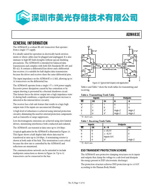
ADM483E GENERAL INFORMATIONThe ADM483E is a robust RS-485 transceiver that operates from a single 5 V supply.It is ideally suited for operation in electrically harsh environ-ments or where cables may be plugged and unplugged. It is also immune to high RF field strengths without special shielding precautions. The ADM483E is intended for balanced data transmission and complies with both EIA Standards RS-485 and RS-422. It contains a differential line driver and a differential line receiver; it is suitable for half-duplex data transmission because the driver and receiver share the same differential pins. The input impedance on the ADM483E is 12 kΩ, allowing up to 32 transceivers on the differential bus.The ADM483E operates from a single 5 V ± 10% power supply. Excessive power dissipation caused by bus contention or by output shorting is prevented by a thermal shutdown circuit. This feature forces the driver output into a high impedance state if, during fault conditions, a significant temperature increase is detected in the internal driver circuitry.The receiver has a fail-safe feature that results in a logic high output state if the inputs are unconnected (floating).A high level of robustness is achieved using internal protection circuitry, eliminating the need for external protection components such as transorbs or surge suppressors.Low electromagnetic emissions are achieved using slew limited drivers, minimizing interference both conducted and radiated. The ADM483E can transmit at data rates up to 250 kbps.A typical application for the ADM483E is illustrated in Figure 23. This figure shows a half-duplex link where data may be transferred at rates up to 250 kbps. A terminating resistor is shown at both ends of the link. This termination is not critical because the slew rate is controlled by the ADM483E and reflections are minimized.The communications network can be extended to include multipoint connections as shown in Figure 26. Up to 32 transceivers can be connected to the bus.612-23 Figure 23. Typical Half-Duplex Link ApplicationTable 6 and Table 7 show the truth tables for transmitting and receiving.1 X = don’t care.1 X = don’t care.ESD TRANSIENT PROTECTION SCHEMEThe ADM483E uses protective clamping structures on its inputs and outputs that clamp the voltage to a safe level and dissipate the energy present in ESD (electrostatic discharge).The protection structure achieves ESD protection up to ±15 kV according to the Human Body Model.ADM483ETYPICAL PERFORMANCE CHARACTERISTICS510152025303540455000.5 1.0 1.5 2.0 2.5OUTPUT LOW VOLTAGE (V)O U T P U T C U R R E N T (m A)06012-003Figure 3. Output Current vs. Receiver Output Low Voltage–30–25–20–15–10–501.52.0 2.53.0 3.54.0 4.55.0OUTPUT HIGH VOLTAGE (V)O U T P U T C U R R E N T (m A)06012-004Figure 4. Output Current vs. Receiver Output High Voltage3.94.04.14.24.34.44.5–40–20020406080TEMPERATURE (°C)O U T P U T H I G H V O L T A G E (V)06012-005Figure 5. Receiver Output High Voltage vs. Temperature 00.10.20.30.40.50.60.70.80.9–40–20020406080TEMPERATURE (°C)O U T P U T L O W V O L T A G E (V)06012-006Figure 6. Receiver Output Low Voltage vs. Temperature5101520253035404500.5 1.0 1.5 2.0 2.5 3.0 3.5 4.0 4.5DIFFERENTIAL OUTPUT VOLTAGE (V)O U T P U T C U R R E N T (m A)06012-007Figure 7. Driver Output Current vs. Differential Output Voltage1.51.61.71.81.92.02.12.22.3–40–20020406080TEMPERATURE (°C)D I F FE R E N T I A L O U T P U T V O L T A G E (V)06012-008Figure 8. Driver Differential Output Voltage vs. TemperatureADM483E20406080100120140024681012OUTPUT LOW VOLTAGE (V)O U T P U T C U R R E N T (m A )06012-009Figure 9. Output Current vs. Driver Output Low Voltage–140–120–100–80–60–40–200–8–6–4–20246OUTPUT HIGH VOLTAGE (V)O U T P U T C U R R E N T (m A )06012-010Figure 10. Output Current vs. Driver Output High Voltage0100200300400500600TEMPERATURE (°C)S U P P L Y C U R R E N T (µA )06012-011Figure 11. ADM483E Supply Current vs. Temperature012345678910–60–40–20020406080100TEMPERATURE (°C)S H U T DO W N C U R R E N T (µA )06012-012Figure 12. Shutdown Current vs. TemperatureCH1 5.00V CH3 500mV CH2 500mV A CH1 2.80V06012-013Figure 13. ADM483E Receiver t PHLCH3 500mV A CH1 2.80V06012-014Figure 14. ADM483E Receiver t PLH Driven by External RS-485 DeviceADM483ETEST CIRCUITS AND SWITCHING CHARACTERISTICS06012-015Figure 15. Driver DC Test Load06012-016Figure 16. Driver Timing Test Circuit5VDI 0V0V +V O –V OV DIFF06012-017Figure 17. Driver Propagation DelaysΩOH06012-018Figure 18. Driver Enable and Disable Times (t DHZ , t DZH , t DZH(SHDN))VOUTV CC DE06012-019Figure 19. Driver Enable and Disable Times (t DZL , t DLZ , t DZL(SHDN))06012-020Figure 20. Receiver Propagation Delay Test CircuitTHE RISE TIME AND FALL TIME OF INPUT A AND INPUT B < 4ns+1V –1VBROV OHV OLA06012-021Figure 21. Receiver Propagation DelaysADM483EOH S1 OPEN S2 CLOSED S3 = +1.5VOHS1 CLOSED S2 OPEN S3 = –1.5V+5V0VV CCV OL06012-022Figure 22. Receiver Enable and Disable Times。
RECOM R5M 5W 隔离 DC DC 电源说明书

DC/DC ConverterDescriptionThe R5M is an isolated 5W DC/DC converter in a compact SMD package available with 4:1 inputs covering 12, 24 and 48V rails providing single or dual regulated, short-circuit protected outputs. There is no minimum load requirement. Isolation is 1.6kVDC/1min, and the operating temperature is from -40°C up to +50°C without derating. Class A and Class B EMC conformity requires only a few external components. Standard packaging is tube.FeaturesRegulated Converters•5W power in SMD package •4:1 Input voltage range •Efficiency up to 86%• 1.6kVDC/1min isolation •Regulated output•-40°C to +50°C at full load•Continuous short circuit protectedR5MSelection GuideModel NumberingY E A Rwa r r a n ty3RoHS 2+compliant 10 from 10Specifications (measured @ Ta= 25°C, nom. Vin, full load and after warm-up unless otherwise stated)Part Input nom. Output Output Efficiency max. CapacitiveNumber Voltage Range (1) Voltage Current typ. (2)Load(3)[VDC] [VDC] [mA] [%] [µF]R5M-xx3.3S/SMD 9-36, 18-75 3.3 1000 774400 R5Mxx05S/SMD 9-36, 18-75 5 1000 812200R5Mxx09S/SMD 9-36, 18-759 55582 1470R5M-xx12S/SMD 9-36, 18-7512 42084-851220 R5M-xx15S/SMD 9-36, 18-7515 333 85-861000R5M-xx24S/SMD 9-36, 18-7524 21082470R5M-xx05D/SMD 9-36, 18-75±5 ±500 82±1000 R5M-xx12D/SMD 9-36, 18-75±12 ±210 84±680 R5M-xx15D/SMD9-36, 18-75±15±168 85±440Notes:Note1: Refer to “Input Voltage Range”Note2: Efficiency is tested at nominal input and full load at +25°C ambient Note3: Max Cap Load is tested at nominal input and full resistive loadBASIC CHARACTERISTICSParameterConditionMin.Typ.Max.Input Voltage Range nom. V IN = 24VDC 9VDC 24VDC 36VDC nom. V IN = 48VDC18VDC48VDC75VDC Input Surge Voltage1 second max.nom. V IN = 24VDC 50VDC nom. V IN = 48VDC 100VDCcontinued on next pageCase Style S ingle/D ualnom. Input Voltage nom. Output VoltageR5M-/SMD5 WattSMDSingle & Dual Outputp re li mi n a rySpecifications (measured @ Ta= 25°C, nom. Vin, full load and after warm-up unless otherwise stated)Specifications (measured @ Ta= 25°C, nom. Vin, full load and after warm-up unless otherwise stated)REGULATIONSParameterConditionValueOutput Accuracy ±1.0% max.Line Regulationlow line to high line, full load±0.2% max.Load Regulation0% to 100% loadsingle 1% max.dual 1% max.10% to 90% loadsingle 0.5% max.dual0.8% max.Cross Regulation asymmetrical 25% / 100% load±5% max.Transient Response Recovery Time25% load step change±500µs typ.PROTECTIONSParameterTypeValueShort Circuit Protection (SCP)continuous, auto recoveryIsolation Voltage (5)I/P to O/P1 minute1.6kVDC min.Isolation Resistance I/P to O/P , V ISO = 500VDC 1G Ω min.Isolation CapacitanceI/P to O/P , 100kHz/0.1V50pF typ.Notes:Note5: This power module is not internally fused. An input line fuse must always be used Recom suggests: 24Vin=T1.25A; 48Vin=T0.63A slow blowp re li mSpecifications (measured @ Ta= 25°C, nom. Vin, full load and after warm-up unless otherwise stated)ENVIRONMENTALParameterConditionValueOperating Temperature Range with derating -40°C to +105°C without derating -40°C to +50°CMaximum Case Temperature measured at “tc point”+105°COperating Humidity non-condensing5% - 95% RH max.Thermal Shock according to MIL-STD-810FVibration according to MIL-STD-810FMTBFaccording to MIL-HDBK-217F, G.B.+25°C2959 x 10³ hoursDerating Graph(@ Chamber and natural convection 0.1m/s)-40-20020407060-30-101030508090120110100100806040907050302010O u t p u t L o a d [%]Ambient Temperature [°C]105i mi n a rySpecifications (measured @ Ta= 25°C, nom. Vin, full load and after warm-up unless otherwise stated)PACKAGING INFORMATIONParameterTypeValuePackaging Dimension (LxWxH)tube 218.0 x 17.2 x 19.9mmPackaging Quantity20pcsStorage Temperature Range non-condensing-55°C to +125°C Storage Humidity5% to 95% RH max.The product information and specifications may be subject to changes even without prior written notice.The product has been designed for various applications; its suitability lies in the responsibility of each customer. The products are not authorized for use in safety-critical applications without RECOM’s explicit written consent. A safety-critical application is an application where a failure may reasonably be expected to endanger or cause loss of life, inflict bodily harm or damage property. The applicant shall indemnify and hold harmless RECOM, its affiliated companies and its representatives against any damage claims in connection with the unauthorizeduse of RECOM products in such safety-critical applications.p r。
max485esa中文资料
General DescriptionThe MAX481, MAX483, MAX485, MAX487–MAX491, andMAX1487 are low-power transceivers for RS-485 and RS-422 communication. Each part contains one driver and onereceiver. The MAX483, MAX487, MAX488, and MAX489feature reduced slew-rate drivers that minimize E MI andreduce reflections caused by improperly terminated cables,thus allowing error-free data transmission up to 250kbps.The driver slew rates of the MAX481, MAX485, MAX490,MAX491, and MAX1487 are not limited, allowing them totransmit up to 2.5Mbps.These transceivers draw between 120µA and 500µA ofsupply current when unloaded or fully loaded with disableddrivers. Additionally, the MAX481, MAX483, and MAX487have a low-current shutdown mode in which they consumeonly 0.1µA. All parts operate from a single 5V supply.Drivers are short-circuit current limited and are protectedagainst excessive power dissipation by thermal shutdowncircuitry that places the driver outputs into a high-imped-ance state. The receiver input has a fail-safe feature thatguarantees a logic-high output if the input is open circuit.The MAX487 and MAX1487 feature quarter-unit-loadreceiver input impedance, allowing up to 128 MAX487/MAX1487 transceivers on the bus. Full-duplex communi-cations are obtained using the MAX488–MAX491, whilethe MAX481, MAX483, MAX485, MAX487, and MAX1487are designed for half-duplex applications.________________________Applications Low-Power RS-485 Transceivers Low-Power RS-422 Transceivers Level Translators Transceivers for EMI-Sensitive Applications Industrial-Control Local Area Networks__Next Generation Device Features o For Fault-Tolerant Applications MAX3430: ±80V Fault-Protected, Fail-Safe, 1/4Unit Load, +3.3V, RS-485 Transceiver MAX3440E–MAX3444E: ±15kV ESD-Protected,±60V Fault-Protected, 10Mbps, Fail-Safe, RS-485/J1708 Transceivers o For Space-Constrained Applications MAX3460–MAX3464: +5V, Fail-Safe, 20Mbps,Profibus RS-485/RS-422 Transceivers MAX3362: +3.3V, High-Speed, RS-485/RS-422Transceiver in a SOT23 Package MAX3280E–MAX3284E: ±15kV ESD-Protected,52Mbps, +3V to +5.5V, SOT23, RS-485/RS-422,True Fail-Safe Receivers MAX3293/MAX3294/MAX3295: 20Mbps, +3.3V,SOT23, RS-485/RS-422 Transmitters o For Multiple Transceiver Applications MAX3030E–MAX3033E: ±15kV ESD-Protected,+3.3V, Quad RS-422 Transmitters o For Fail-Safe Applications MAX3080–MAX3089: Fail-Safe, High-Speed (10Mbps), Slew-Rate-Limited RS-485/RS-422Transceiverso For Low-Voltage ApplicationsMAX3483E/MAX3485E/MAX3486E/MAX3488E/MAX3490E/MAX3491E: +3.3V Powered, ±15kVESD-Protected, 12Mbps, Slew-Rate-Limited,True RS-485/RS-422 Transceivers For pricing, delivery, and ordering information, please contact Maxim Direct at1-888-629-4642, or visit Maxim Integrated’s website at .______________________________________________________________Selection Table19-0122; Rev 10; 9/14PARTNUMBERHALF/FULL DUPLEX DATA RATE (Mbps) SLEW-RATE LIMITED LOW-POWER SHUTDOWN RECEIVER/DRIVER ENABLE QUIESCENT CURRENT (μA) NUMBER OF RECEIVERS ON BUS PIN COUNT MAX481Half 2.5No Yes Yes 300328MAX483Half 0.25Yes Yes Yes 120328MAX485Half 2.5No No Yes 300328MAX487Half 0.25Yes Yes Yes 1201288MAX488Full 0.25Yes No No 120328MAX489Full 0.25Yes No Yes 1203214MAX490Full 2.5No No No 300328MAX491Full 2.5No No Yes 3003214MAX1487 Half 2.5No No Yes 2301288Ordering Information appears at end of data sheet.找电子元器件上宇航军工MAX481/MAX483/MAX485/MAX487–MAX491/MAX1487Low-Power, Slew-Rate-LimitedRS-485/RS-422 TransceiversPackage Information For the latest package outline information and land patterns, go to . Note that a “+”, “#”, or “-”in the package code indicates RoHS status only. Package drawings may show a different suffix character, but the drawing pertains to the package regardless of RoHS status.16Low-Power, Slew-Rate-Limited RS-485/RS-422 TransceiversMAX481/MAX483/MAX485/MAX487–MAX491/MAX1487Maxim Integrated cannot assume responsibility for use of any circuitry other than circuitry entirely embodied in a Maxim Integrated product. No circuit patent licenses are implied. Maxim Integrated reserves the right to change the circuitry and specifications without notice at any time. The parametric values (min and max limits) shown in the Electrical Characteristics table are guaranteed. Other parametric values quoted in this data sheet are provided for guidance.Maxim Integrated 160 Rio Robles, San Jose, CA 95134 USA 1-408-601-100017©2014 Maxim Integrated Products, Inc.Maxim Integrated and the Maxim Integrated logo are trademarks of Maxim Integrated Products, Inc.。
索菲玛滤清器产品车型对应表
HE-480R 半导体清洁过程中的电导度计说明书

Repeatability
Within ±0.5ˋ of the full scale (in equivalent inputʣ
Linearity
Within ±0.5ˋ of the full scale (in equivalent inputʣ
Transmission output
4mA to 20mA DC : input/output isolated type
˙ Converter HE-480R
Panel Cut Size
45
+0.6 0
130 (min.)
+0.8 0
92
70 (min.)
˙Resistivity sensor ERF-001 Series
Cable-attached type
Connector type
Water-proof Connector
Unit
kЊɾm
182.3ʢstandardʣ, 181.8, 182.4 Shown on the Left.
When the measured value is above the upper limit of the measurement range derived from
the specified specific resistance, the specified resistance is used as the measured value.
˔High precision temperature compensation
The HE-480R employs a platinum temperature resistor (Pt1000Њ) in its temperature compensation element, thereby enabling high precision temperature compensation in the range of 0 to 100°C.
˔Selectable temperature compensation function
REC3-4805SRWZ中文资料
Safe Operating Area
100 50 75 125 80 105 Operating Temperature (°C) 0 25
Output Power (%)
-55°C to +125°C 95% RH Non-Conductive Plastic 20°C/W for metal case 13g 1043 x 10 hours 186 x 103 hours
3 Watt DIP24 & SMD Single & Dual Output
EN-60950-1 Certified UL-60950-1 Certified EN-60601-1 Certified
Description
4:1 Input * add suffix /H4 for 4kVDC isolation or /H6 (REC3-S/DRWZ(H4/H6)) for 6kVDC isolation xx = 9-36Vin = 24 * add suffix "/A" or "/C" for Pinning, see next page xx = 18-72Vin = 48 “B” Pinning is NOT available for this series ! * add suffix "/M" for metal case * add suffix "/SMD" for SMD package e.g. REC3-2412SRW/H4/AM = 4kVDC isol. / Pinout "A" / metal case
Notes :
1. If the options "/M" for metal case and "/SMD" for SMD pinout are combined, the maximum allowed isolation voltage is 2kVDC because of the shorter distances between pins and the metal case, so only available SMD-option in metal-case is "/H2". DIP-24 through-hole case and SMD-plastic case are not affected and offer the full isolation barriers of 4kVDC for "/H4" option and 6kVDC for "/H6".
REC-50M 操作说明书
ATION MANUALREC-50MRead and understand all of the instructions and safety informationin this manual before operating or servicing this tool.REGISTRATION/ TABLE OF CONTENTSTHANK YOU...for purchasing an Huskie Tools product. Our mission is to supply the finest steel cableconnecting and cutting tools and cable-related products to the transmission and distribution markets. Huskie Tools products will represent state-of-the-art tools and be dependable and safe. All products will carry an unconditionalguarantee to be free from defects and to perform as advertised.Please take the time to read this manual carefully to learn how to correctly operate and maintain your tool.WARRANTYWarrantyHuskie Tools products carry a warranty that makes us a leader in the tool industry. No other manufacturer dares to back its tools as we do.All Huskie REC-SERIES battery operated products carry a 5 year warranty. The ECO-SERIES battery operated products carry a 1 year warranty. The BP-80 & BP-84 batteries carry a 5 year warranty from the date stamped on the battery. The BP-82 battery carries a 1 year warranty.PRODUCT WARRANTYREC-Series battery operated products 5 Y earsECO-Series battery operated products 1 Y earsBatteries (BP-80, BP-84) 5 years/ (BP-82) 1 yearChargers (CH-90, CH-94) 5 Y earsThe warranty does not cover any damages incurred from a Huskie tool including damages to property, bodily injuries and lost wages resulting from such injuries. This warranty solely covers the repair or replacement of tools supplied by Huskie. These remedies are exclusive, and the total liability of Huskie Tools, LLC whether based on contract, warranty, negligence, indemnification, strict liability or otherwise, shall not exceed the purchase price of the tool. In no event shall Huskie Tools, LLC be liable for consequential, incidental or special damages.HUSKIE TOOLS, LLC MAKES NO OTHER WARRANTIES OF ANY KIND, EXPRESSED OR IMPLIED, AND ALL IMPLIED WARRANTIES INCLUDING ANY WARRANTY OF MERCHANTABILITY AND FITNESS FOR A PARTICULAR PURPOSE ARE DISCLAIMED.Huskie reserves the right to determine all warranty claims. Huskie will not warranty tools containing parts or batteries not originally supplied by Huskie. Failure due to misuse, improper maintenance, misapplication, not following instructions or warnings, abuse or repairs attempted by anyone other than Huskie Tools, LLC, or an authorized service center renders this warranty null and void.Repair and Warranty ClaimsAll claims must be sent to Huskie for inspection and authorization. A Return Goods Authorization (RGA) is required before shipping tools to Huskie. Secure the authorization by telephoning or writing to Huskie’s main office with detailsof the claim. Non-warranty repairs are handled using the same procedure. Repairs exceeding 50 percent of the cost of a new tool will be advised before repairs are made.Payment TermsUpon credit approval Huskie’s standard payment terms are net-30 days. Visa, Mastercard, Discover and American Express are also accepted.FreightAll Huskie tools are FOB, Glendale Heights, Illinois. Goods will be shipped pre-paid and added, unless otherwise specified. Freight shipments over $17,000 are pre-paid.QuotationsSpecial quantity quotations should be phoned in to discuss the scope of your tool requests.Complete Support ServicesOur customers have direct access to us for training, service, and problem solving. As specialists in tools, we maintaina trained repair staff and a large stock of parts. This contrasts with many tool suppliers who carry tools as a sideline without offering support services. Here are some reasons why our customers love to do business with us:• Quick delivery• We maintain inventory at our headquarters.• Training and troubleshooting services.• Fast repair service.• Design and engineering service for special tool needs.SAFETYThis safety alert symbol indicates a potential per-Electric Shock hazard:Pinch Point Hazard:Compression Dies at high force can cause severe per-sonal injury. Keep all bodyKIT INCLUDESBattery and Charger• BP-84 Huskie Tools Lithium Ion Battery • CH-94 Huskie Tools Charger• This charger can charge the BP-84, BP-82 and BP-80 only. Huskie Tools batteries, including the BP-70, BP-70EI and the BP-70MH must be charged with the CH-90, CH-80, or previous charger models.• 1 Battery Powered Tool • 1 Carrying Case • 1 CH-94 Charger• 2 BP-84 Lithium Ion Batteries •1 Carrying StrapSPECIFICATIONSREC-50MThe REC-50M battery operated slicing tool cuts 2” cable with the touch of a finger. It features a powerful gear reduction motor that pulls a moveable blade through the toughest copper and aluminum cables.The REC-50M comfortably fits into the lineman’s gloved hand, and repetitive ratcheting movement is entirely eliminated. Just a squeeze of the rocker arm trigger is all it takes to make a cut and almost no muscle power is needed. As a result, the risk of sprains, strains, and lost time due to muscle related injuries can be significantly reduced. The moveable blade has wide gear teeth for extra power and full cutting traction. Gear guides are attached on both ends of the movable blade to align the gear teeth with the internal pinion gear.OPERATING INSTRUCTIONS CHARGING THE BATTERY1. Insert the plug end into a 120V power source. The LED (Power) indicator willbe steady green indicating the charger is now in “stand-by” mode and ready tocharge the battery. Do not plug the charger into a generator as this will likelycause the fuse in the charger to short, and will not operate.2. To charge a drained battery, insert the battery into the charger. The LEDindicator shows a steady amber while charging. A depleted battery will becompletely charged in approximately 50-70 minutes. The LED indicator will showa steady green when the battery is fully charged.3. If the LED indicator goes out or is flashing quick amber, this could be a possibleshort in the battery circuit, or a problem with the charger itself. It is best to consultthe factory at 1-800-860-6170 for service if such a condition occurs.4. For technical questions or difficulty in operation, please call our customerservice department at 1-800-860-6170.ATTACHING THE BATTERY CARTRIDGE1. While pressing the latch, pull out the battery cartridge. T o replace the batterycartridge, push the new cartridge firmly into place.2. After inserting a battery cartridge, check that it is securely inplace by pulling gently. Do not press the latch when pulling the cartridge.TRIGGER AND RELEASE BUTTON1. The ram advances when the trigger is pressed and stops when the trigger isreleased.2. To retract the ram, push the release button. The ram continues to retract whilethe release button is pressed.CUTTING1. Retract blades by pressing the release button.2. Be sure that material being cut is within the specified cutting capacity of the tool.3. Place the material to be cut between the blades and press the advance trigger until blades hold the material in place.4. Check material for proper alignment to the cutting blades. It should be at a 90° degree angle to the blades. Any other angle will cause the blades to spread apart and possibly break.5. Continue to advance the blades until the material is cut. If material is cut and tool has not yet by passed, it may be difficult to retract blades. If this occurs, continue to advance tool and build pressure. A series of clicks will be heard while the tool running in a “neutral” mode. This indicates that the tool has built full pressure and bypassed and can now be released.MAINTENANCE AND INSPECTION1. Daily maintenance is required to ensure that the tool is kept in good working condition.2. Sharpen blades occasionally with a sharpening stone on the back side of the blades to remove any burrs that may occur.3. Do not store the tool in a humid environment.4. Wipe away any excess oil with a soapy cloth.5. Provided that maintenance of the tool is carried out regularly, the tool should providemany years of service.6. Should you experience any difficulty with the operation and maintenance of this tool,contact Huskie’s technical support department at 1-800-860-6170.PRECAUTION FOR THE TOOLPRECAUTION FOR THE CHARGER1. Select appropriate dies for the connector to be compressed. Incorrect combinations result in inferior connections of the conductors. Consult your connector manufacturer for the recommended die/connector combinations.2. Always point the tool AWAY from other people.3. If the tool is stored for an extended period at a temperature of less than 25º F (-5ºC), the tool should be allowed to return to room temperature to ensure smooth operation Use the tool only after it has been at room temperature for 1 hour.4. Do not drop the tool. Dropping the tool may damage the hydraulic circuit and result in the tool not functioning correctly.5. Keep the head and ram clean and free of debris. Solvents can be used to clean the head, but should not be used on the plastic body. Use soap and water to clean the body.6. Do not use tool for continous use. If any sign of over heating, allow the tool to cool for 15 mins.7. Do not allow tool to be submerged in water. The tool may be used in damp or wet environ-ments. However it is recommended for tool to be air-dried before use.PRECAUTION FOR THE BATTERY CARTRIDGE1. Do not short circuit the contacts or expose the cartridge to water, oil or solvents.2. Do not disassemble or attempt to repair the battery cartridge or dispose of in a fire.3. Do not drop or otherwise abuse the battery cartridge.4. Do not leave the cartridge in locations where it will be exposed to a temperature greater than 140ºF (60ºC) for an extended period.5. The battery has a limited life. When the crimping capacity becomes about 1/2 that of the original capacity, the battery should be replaced.6. If the battery cartridge is stored without being charged, natural drainage will cause the power to be reduced. The battery should be charged every 3 months if not in use.1. The LED indicator lights up amber and remains lit when the unit starts charging a battery cartridge. The indicator turns green when charging is completed.2. The BP-84 can be charged with any of the Huskie Lithium-Ion chargers including the CH-80, CH-90 & CH-94.3. Allow battery cartridges to cool before charging. Allow at least 15 minutes between charges when charging several cartridges in succession.4. Charge batteries at an ambient temperature of 50º-95ºF (10º-35º C). Charging time is approximately 50-70 minutes for the BP-84.5. Never short circuit the output terminals.6. Do not expose the charger to water, oil or solvents.7. Do not disassemble, attempt to modify, drop or otherwise abuse charger.BREAKDOWNPARTS LISTNO.DESCRIPTION CODE QTY.11 M3 X 3 Screw RC50-03 212 Gear Guide (B) RC50-04 113 Moving Blade RC50-16 114 Shoulder Screw RC50-05 115 Gear Guide (A) RC50-15 116 Stationary Blade RC50-18 117 M6 Lock Washer (Ni) RC50-06 118 M6 Lock Nut RC50-07 119 M3 X 8 Screw RC50-08 520 Bearing Case RC50-10 121 Cutter Plate RC50-11 122 M5 X 14 Screw RC50-09 1123 Bearing 6001 RC50-12 124 Pinion Gear RC50-13 125 Bearing 6002 RC50-14 126 Needle Pin 3 X 11.8 RC50-17 227 Gear Case Ass'y RC50-19 128 M4 X 8 Screw RC50-20 229 Gear RC50-21 130 Gear Plate RC50-22 231 Gear Cover RC50-23 132 Housing Set 50M-HS 133 Hanging Strap 558-07A 134 M3 X 14 Screw (T.P.) RC50-01 235 M4 X 20 Screw 558-01 937 Brush RC50-32 138 Motor 50M- Motor 139 Switch Unit Ass'y 50M- Switch 140 Switch Knob RC50-29 141 Spring (524) RC50-30 142 Switch Lock RC50-31 1TROUBLESHOOTING GUIDENOTESNOTESNOTES195 Internationale Blvd Glendale Heights, IL 60139 Phone 800-860-6170Fax 800-345-3767。
- 1、下载文档前请自行甄别文档内容的完整性,平台不提供额外的编辑、内容补充、找答案等附加服务。
- 2、"仅部分预览"的文档,不可在线预览部分如存在完整性等问题,可反馈申请退款(可完整预览的文档不适用该条件!)。
- 3、如文档侵犯您的权益,请联系客服反馈,我们会尽快为您处理(人工客服工作时间:9:00-18:30)。
2.54
2.54
110
January-2007
20 0
Safe Operating Area
0 50 150
20 0 -40
Safe Operating Area
0 50 150
100 80 105 96 Operating Temperature °C -40
100 85 105 98 Operating Temperature °C
Package Style and Pinning (mm) Wide Input 2:1
Vout2(VDC) at Vout2(mA)
EN-60950-1 Certified EN-60601-1 Certified UL-60950-1 Certified
* V1 min. load 100mA to supply V2 well * add suffix "M" for Metal Case, e.g. REC3-240505DRWI/AM For alternative custom output voltage and power combinations, please contact Recom Technical Support
元器件交易网
ECONOLINE
DC/DC-Converter
Specifications (Core Operating Area)
Relative Humidity Case Material Thermal Impedance Package Weight MTBF (+25°C) (+80°C)
ECONOLINE
DC/DC-Converter
REC3DRWI/A Series
3 Watt DIP24 Isolated Dual Output
Selection Guide
Part Number DIP24 REC3-050505DRWI/A REC3-050509DRWI/A REC3-050512DRWI/A REC3-050515DRWI/A REC3-120505DRWI/A REC3-120509DRWI/A REC3-120512DRWI/A REC3-120515DRWI/A REC3-240505DRWI/A REC3-240509DRWI/A REC3-240512DRWI/A REC3-240515DRWI/A REC3-480505DRWI/A REC3-480509DRWI/A REC3-480512DRWI/A REC3-480515DRWI/A Input Voltage (VDC) 4.5-9 4.5-9 4.5-9 4.5-9 9-18 9-18 9-18 9-18 18-36 18-36 18-36 18-36 36-72 36-72 36-72 36-72 Output Voltage Vout1(VDC) 5 5 5 5 5 5 5 5 5 5 5 5 5 5 5 5 Output Current at Vout1(mA) 300* 300* 300* 300* 300* 300* 300* 300* 300* 300* 300* 300* 300* 300* 300* 300* Output Voltage 5 9 12 15 5 9 12 15 5 9 12 15 5 9 12 15 Output Current 300 167 125 100 300 167 125 100 300 167 125 100 300 167 125 100
3rd angle projection
24 PIN DIP Package
32.00 10.20 3.81 4.60 0.51
20.30
Pin Connections Pin # 2 3 Dual –Vin –Vin +Vout 2 –Vout 2 +Vout 1 –Vout 1 +Vin +Vin
Detailed Information see Application Notes chapter "MTBF"
ctive Plastic Natural convection using MIL-HDBK 217F using MIL-HDBK 217F 20°C/W for metal case 13g 877 x 103 hours 138 x 103 hours
Specifications (Core Operating Area)
Input Voltage Range Output Voltage Accuracy Line Voltage Regulation Load Voltage Regulation (10% to 100% full load ) Output Ripple and Noise (at 20MHz BW) Operating Frequency No Load Power Consumption Isolation Voltage Input / Output (tested for 1 second) Vout1 / Vout2 (tested for 1 second) Rated Working Voltage (long term isolation) Isolation Capacitance Isolation Resistance Short Circuit Protection (V1) Operating Temperature Range (free air convection) Storage Temperature Range Vin=5V Vin=12, 24, 48V 2:1 ±2% max. ±0.4% max. ±0.6% max. 50mVp-p max. 100kHz typ. 300mW max. 2000VDC min. 500VDC min. see Application Notes 40pF typ. 1 GΩ min. Continuous -40°C to +80°C (see Graph) -40°C to +85°C (see Graph) -55°C to +125°C continued on next page January-2007 109
Derating-Graph
(Ambient Temperature)
Vin = 5V
100 80 (2W) 67 60 (1.5W) 50 40
Vin = 12, 24, 48V
100 80 (2W) 67 60 (1.5W) 50 40
Output Power (%)
Output Power (%)
元器件交易网
Features
Regulated Converters
● ● ● ● ● ● ●
3W DIP Package Isolated Dual Outputs Vout1 / Vout2 Input / Output 2KVDC Isolation min. UL94V-0 Package Material Continuous Short Circuit Protection Auto-Restarting (V1) Wide Input 2:1 Internal SMD design 100% Burned In
15.24
9 11 14 16 22 23
Recommended Footprint Details
1.00 ø+0.15/0
2 3 Bottom View 23 22 16 14 Top View 9 11
NC = No Connection XX.X ± 0.5 mm XX.XX ± 0.25 mm