FCN-244D050-B中文资料
DIN 2445-1
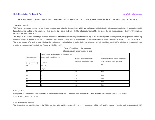
DIN 2445 Part-1 SEAMLESS STEEL TUBES FOR DYNAMIC LOADS HOT FINISHED TUBES NOMINAL PRESSURES 100 TO 400
Global Marketing for Tube & Pipe
Recommendation R 336. *) Designated in DIN 24312 (at present in draft form) with PN
**) If the pipeline length l, rate of flow w and closing time Ts vary considerably from those indicated in Table 1, the pressure surges △p can be varied and taken from the straight-line graph. The pressure surges must then not be greater than △p = 60 bar Table 2. Normal pressure of the installation (design pressure) = 100 bar Maximum applicable pressure (calculated pressure for tubes) = 160 bar = 16 N/mm²
2. Designation Designation of a seamless steel tube of 88.9 mm outside diameter and 11 mm wall thickness of St 52.4 with delivery test according to DIN 1629 Part 4: Tube 88.9 X 11 DIN 2448 - St 52.4 3. Dimensions and weights The dimensions and weights given in the Tables for pipes with wall thicknesses of up to 25 mm comply with DIN 2448 and for pipes with greater wall thicknesses with ISO
DS244中文资料
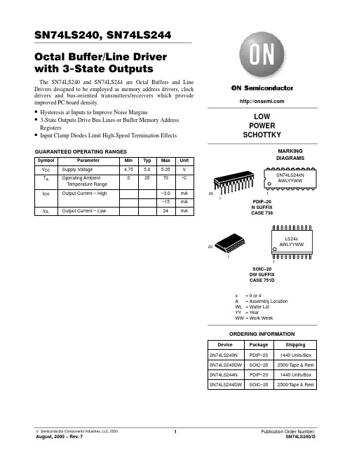
SN74LS240, SN74LS244 Octal Buffer/Line Driver with 3-State OutputsThe SN74LS240 and SN74LS244 are Octal Buffers and Line Drivers designed to be employed as memory address drivers, clock drivers and bus-oriented transmitters/receivers which provide improved PC board density.•Hysteresis at Inputs to Improve Noise Margins•3-State Outputs Drive Bus Lines or Buffer Memory Address Registers•Input Clamp Diodes Limit High-Speed Termination Effects GUARANTEED OPERATING RANGESLOWPOWERSCHOTTKYDevice Package ShippingORDERING INFORMATIONSN74LS240N PDIP–201440 Units/Box SN74LS240DW SOIC–202500/T ape & ReelPDIP–20N SUFFIXCASE 738201201SN74LS244N PDIP–201440 Units/Box SN74LS244DW SOIC–202500/T ape & Reelx= 0 or 4A= Assembly LocationWL= Wafer LotYY= YearWW= Work WeekSN74LS24xNAWLYYWWMARKINGDIAGRAMSLS24xAWLYYWWSOIC–20DW SUFFIXCASE 751D11LOGIC AND CONNECTION DIAGRAMS DIP (TOP VIEW)2G2G SN74LS240SN74LS244TRUTH TABLESH = HIGH Voltage Level L = LOW Voltage Level X = ImmaterialZ = HIGH Impedance(unless otherwise specified)AC WAVEFORMSFigure 4.PACKAGE DIMENSIONSN SUFFIXPLASTIC PACKAGE CASE 738–03ISSUE ENOTES:1.DIMENSIONING AND TOLERANCING PER ANSI Y14.5M, 1982.2.CONTROLLING DIMENSION: INCH.3.DIMENSION L TO CENTER OF LEAD WHEN FORMED PARALLEL.4.DIMENSION B DOES NOT INCLUDE MOLD FLASH.DIM MIN MAX MIN MAX MILLIMETERSINCHES A 25.6627.171.010 1.070B 6.10 6.600.2400.260C 3.81 4.570.1500.180D 0.390.550.0150.022G 2.54 BSC 0.100 BSC J 0.210.380.0080.015K 2.80 3.550.1100.140L 7.62 BSC 0.300 BSC M 0 15 0 15 N0.51 1.010.0200.040____E 1.27 1.770.0500.070F 1.27 BSC 0.050 BSCD SUFFIX PLASTIC SOIC PACKAGE CASE 751D–05ISSUE FNotesON Semiconductor and are trademarks of Semiconductor Components Industries, LLC (SCILLC). SCILLC reserves the right to make changes without further notice to any products herein. SCILLC makes no warranty, representation or guarantee regarding the suitability of its products for any particular purpose, nor does SCILLC assume any liability arising out of the application or use of any product or circuit, and specifically disclaims any and all liability, including without limitation special, consequential or incidental damages. “Typical” parameters which may be provided in SCILLC data sheets and/or specifications can and do vary in different applications and actual performance may vary over time. All operating parameters, including “Typicals” must be validated for each customer application by customer’s technical experts. SCILLC does not convey any license under its patent rights nor the rights of others.SCILLC products are not designed, intended, or authorized for use as components in systems intended for surgical implant into the body, or other applications intended to support or sustain life, or for any other application in which the failure of the SCILLC product could create a situation where personal injury or death may occur. Should Buyer purchase or use SCILLC products for any such unintended or unauthorized application, Buyer shall indemnify and hold SCILLC and its officers, employees, subsidiaries, affiliates, and distributors harmless against all claims, costs, damages, and expenses, and reasonable attorney fees arising out of, directly or indirectly, any claim of personal injury or death associated with such unintended or unauthorized use, even if such claim alleges that SCILLC was negligent regarding the design or manufacture of the part. SCILLC is an Equal Opportunity/Affirmative Action Employer. PUBLICATION ORDERING INFORMATIONCENTRAL/SOUTH AMERICA:Spanish Phone:303–308–7143 (Mon–Fri 8:00am to 5:00pm MST)Email:ONlit–spanish@ASIA/PACIFIC: LDC for ON Semiconductor – Asia SupportPhone:303–675–2121 (Tue–Fri 9:00am to 1:00pm, Hong Kong Time)Toll Free from Hong Kong & Singapore:001–800–4422–3781Email: ONlit–asia@JAPAN: ON Semiconductor, Japan Customer Focus Center4–32–1 Nishi–Gotanda, Shinagawa–ku, Tokyo, Japan 141–0031Phone: 81–3–5740–2745Email: r14525@。
贴片元件标记对应型号资料
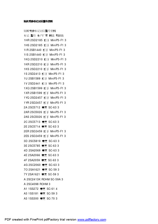
贴片元件标记对应型号资料贴片元件标记对应型号资料标记型号生产厂家封装引脚数1HR 2SD2185 松下MiniP3-F1 3 1HS 2SD2185 松下MiniP3-F1 3 1IR 2SB1440 松下MiniP3-F1 3 1IS 2SB1440 松下MiniP3-F1 3 1KQ 2SD2210 松下MiniP3-F1 3 1KR 2SD2210 松下MiniP3-F1 3 1KS 2SD2210 松下MiniP3-F1 3 1S 2SD2413 松下MiniP3-F1 3 1U 2SB1589 松下MiniP3-F1 3 1V 2SD2441 松下MiniP3-F1 3 1XQ 2SB1599 松下MiniP3-F1 3 1XR 2SB1599 松下MiniP3-F1 3 1YQ 2SD2457 松下MiniP3-F1 3 1YR 2SD2457 松下MiniP3-F1 3 2A 2SC5712 東芝SC-63 32AR 2SC5026 松下MiniP3-F1 3 2AS 2SC5026 松下MiniP3-F1 3 2C 2SC5713 東芝SC-63 32E 2SC5714 東芝SC-63 32ER 2SD2459 松下MiniP3-F1 3 2ES 2SD2459 松下MiniP3-F1 3 3D 2SC5819 東芝SC-63 33E 2SC5785 東芝SC-63 34D 2SA2069 東芝SC-63 34E 2SA2066 東芝SC-63 34F 2SA2059 東芝SC-63 34G 2SC2060 東芝SC-63 37O 2SA1621 東芝SC-59 37Y 2SA1621 東芝SC-59 3A 2SC2413K ROHM SC-59A 3 A 2SC4098 ROHM 3A1 1SS272 東芝SC-61 4A3 1SS181 東芝SC-59 3A3 1SS300 東芝SC-70 3A4 1SS319 東芝SC-61 4A4 1SS383 東芝4A5 1SS384 東芝SOT-343 4A5 1SS391 東芝SC-61 4A6 HN2S01F 東芝SC-74 6A6 HN2S01FU 東芝SC-88 6 A7 1SS402 東芝SOT-343 4A9 1SS294 東芝SC-59 3AL 2SA1971 東芝SC-63 3AL 2SC5307 東芝SC-63 3AN 2SC2532 東芝SC-59 3 AO 2SA2880 東芝SC-63 3 AQ 2SB766 松下MiniP3-F1 3 AR 2SB766 松下MiniP3-F1 3 AS 2SB766 松下MiniP3-F1 3 AU 2SB804 NEC SC-62 3AV 2SB804 NEC SC-62 3AW 2SB804 NEC SC-62 3AY 2SA2880 東芝SC-63 3B 2CS4081 ROHM 3B 2SC2412K ROHM SC-59A 3 B3 1SS184 東芝SC-59 3B3 1SS301 東芝SC-70 3B9 1SS311 東芝SC-59 3B9 1SS397 東芝SC-70 3BD 1SS271 東芝SC-59 3BE 1SV172 東芝BF 1SS268 東芝SC-59 3BG 1SS269 東芝SC-59 3BH 1SS295 東芝SC-59 3BO 2SA1200 東芝SC-63 3 BQ 2SB766A 松下MiniP3-F1 3 BR 2SB766A 松下MiniP3-F1 3 BS 2SB766A 松下MiniP3-F1 3 BU 2SD1005 NEC SC-62 3BU DA228K ROHM SC-59 3 BU DA228U ROHM SC-70 3 BV 2SD1005 NEC SC-62 3BW 2SD1005 NEC SC-62 3BY 2SA1200 東芝SC-63 3C 2SC2411K ROHM SC-59A 3C 2SC4097 ROHM 3C1 1SS352 東芝C1 1SS387 東芝C3 1SS226 東芝SC-59 3C9 1SS307 東芝SC-59 3CEO 2SC3325 東芝SC-59 3 CEY 2SC3325 東芝SC-59 3CG 2SA1163 東芝SC-59 3CK 2SD999 NEC SC-62 3CL 2SD999 NEC SC-62 3CM 2SD999 NEC SC-62 3CO 2SC2881 東芝SC-63 3CO 2SC4209 東芝SC-59 3CQ 2SB767 松下MiniP3-F1 3 CR 2SB767 松下MiniP3-F1 3 CY 2SC2881 東芝SC-63 3CY 2SC4209 東芝SC-59 3D 2SA1037KLN ROHM SC-59A 3 D3 1SS187 東芝SC-59 3DG 2SC2713 東芝SC-59 3DK 2SB798 NEC SC-62 3DL 2SB798 NEC SC-62 3DM 2SB798 NEC SC-62 3DO 2SA1201 東芝SC-63 3DQ 2SB789 松下MiniP3-F1 3 DR 2SB789 松下MiniP3-F1 3 DY 2SA1201 東芝SC-63 3E3 1SS190 東芝SC-59 3EK 2SD1001 NEC SC-62 3EL 2SD1001 NEC SC-62 3EM 2SD1001 NEC SC-62 3EO 2SC2882 東芝SC-63 3EQ 2SB789A 松下MiniP3-F1 3 ER 2SB789A 松下MiniP3-F1 3 EX 2SD2402 NEC SC-62 3EY 2SC2882 東芝SC-63 3EY 2SD2402 NEC SC-62 3EZ 2SD2402 NEC SC-62 3F 2SA1037K ROHM SC-59A 3 F 2SA1576 ROHM 3F3 1SS193 東芝SC-59 3F5 1SS250 東芝SC-59 3F5 1SS370 東芝SC-70 3F5 1SS403 東芝SOD-323 2F9 1SS321 東芝SC-59 3FK 2SB800 NEC SC-62 3FL 2SB800 NEC SC-62 3FM 2SB800 NEC SC-62 3FO 2SA1202 東芝SC-63 3FX 2SB1571 NEC SC-62 3FY 2SA1202 東芝SC-63 3FY 2SB1571 NEC SC-62 3FZ 2SB1571 NEC SC-62 3G3 1SS196 東芝SC-59 3G3 2SA1455K ROHM SC-59A 3 GK 2SD1615 NEC SC-62 3GL 2SD1615 NEC SC-62 3GM 2SD1615 NEC SC-62 3 GO 2SC2883 東芝SC-63 3 GP 2SD1615A NEC SC-62 3 GQ 2SD1615A NEC SC-62 3 GX 2SD2403 NEC SC-62 3GY 2SC2883 東芝SC-63 3GY 2SD2403 NEC SC-62 3GZ 2SD2403 NEC SC-62 3H9 1SS344 東芝SC-59 3HK 2SD1006 NEC SC-62 3HL 2SD1006 NEC SC-62 3HM 2SD1006 NEC SC-62 3 HO 2SA1203 東芝SC-63 3HP 2SD1007 NEC SC-62 3HQ 2SD1007 NEC SC-62 3HR 2SD1007 NEC SC-62 3HR 2SB956 松下MiniP3-F1 3 HS 2SB956 松下MiniP3-F1 3 HX 2SB1572 NEC SC-62 3HY 2SA1203 東芝SC-63 3HY 2SB1572 NEC SC-62 3HZ 2SB1572 NEC SC-62 3I9 1SS336 東芝SC-59 3IK 2SA1463 NEC SC-62 3IL 2SA1463 NEC SC-62 3IO 2SC3515 東芝SC-63 3IQ 2SB1073 松下MiniP3-F1 3 IR 2SC3515 東芝SC-63 3IR 2SB1073 松下MiniP3-F1 3 J 2SC2059K ROHM SC-59A 3J 2SC4099 ROHM 3J9 1SS337 東芝SC-59 3JO 2SA1384 東芝SC-63 3JR 2SK208 東芝SC-59 3JR 2SA1384 東芝SC-63 3K DA221 ROHM SC-75A 3K DA204U ROHM SC-70 3K DA204K ROHM SC-59 3K9 1SS348 東芝SC-59 3KA 2SC4409 東芝SC-63 3KD 2SC4541 東芝SC-63 3KK 2SB805 NEC SC-62 3KL 2SB805 NEC SC-62 3KM 2SB805 NEC SC-62 3KP 2SB806 NEC SC-62 3KQ 2SB806 NEC SC-62 3KR 2SB806 NEC SC-62 3L 2SC2412KLN ROHM SC-59A 3 L9 1SS349 東芝SC-59 3LA 2SA1681 東芝SC-63 3LD 2SA1736 東芝SC-63 3LK 2SD1000 NEC SC-62 3LL 2SD1000 NEC SC-62 3LM 2SD1000 NEC SC-62 3MK 2SB799 NEC SC-62 3 ML 2SB799 NEC SC-62 3 MM 2SB799 NEC SC-62 3 MO 2SC2873 東芝SC-63 3 MY 2SC2873 東芝SC-63 3 N9 1SS372 東芝SC-70 3 N9 1SS374 東芝SC-59 3 NA 2SK1273 NEC SC-62 3 NB 2SK1586 NEC SC-62 3 NC 2SK1485 NEC SC-62 3 ND 2SK1583 NEC SC-62 3 NE 2SK1585 NEC SC-62 3 NF 2SK1587 NEC SC-62 3 NG 2SK1588 NEC SC-62 3 NH 2SK1584 NEC SC-62 3 NI 2SK1586 NEC SC-62 3 NJ 2SK2111 NEC SC-62 3 NK 2SC2780 NEC SC-62 3 NL 2SC2780 NEC SC-62 3 NM 2SC2780 NEC SC-62 3 NO 2SA1213 東芝SC-63 3 NO 2SK1592 NEC SC-62 3 NP 2SK1593 NEC SC-62 3 NQ 2SK1959 NEC SC-62 3 NR 2SK1960 NEC SC-62 3 NS 2SK2109 NEC SC-62 3 NT 2SK2110 NEC SC-62 3 NV 2SK2112 NEC SC-62 3 NW 2SK2159 NEC SC-62 3 NX 2SK2857 NEC SC-62 3 NY 2SA1213 東芝SC-63 3 O9 1SS377 東芝SC-59 3 O9 1SS378 東芝SC-70 3 O9 1SS385 東芝SC-75 3 O9 1SS385F 東芝SC-81 3 OK 2SC3736 NEC SC-62 3 OL 2SC3736 NEC SC-62 3PA 2SJ179 NEC SC-62 3PB 2SJ197 NEC SC-62 3PC 2SJ199 NEC SC-62 3PD 2SJ205 NEC SC-62 3PE 2SJ207 NEC SC-62 3PF 2SJ208 NEC SC-62 3PH 2SJ206 NEC SC-62 3PO 2SC2884 東芝SC-63 3 PO 2SJ212 NEC SC-62 3PP 2SJ213 NEC SC-62 3PQ 2SJ355 NEC SC-62 3PR 2SJ356 NEC SC-62 3PY 2SC2884 東芝SC-63 3 QO 2SC2714 東芝3R12 UMR12N ROHM SC-88 6 R23 2SC3356 Q NEC SC-59 3 R24 2SC3356 R NEC SC-59 3 R25 2SC3356 S NEC SC-59 3 R9 1SS392 東芝SC-59 3R9 1SS393 東芝SC-70 3RQ 2SD1280 松下MiniP3-F1 3 RR 2SD1280 松下MiniP3-F1 3 RS 2SD1280 松下MiniP3-F1 3 S2 1SS315 東芝SC-59 3S9 1SS394 東芝SC-59 3SA 2SC2982 東芝SC-63 3SK 2SC3554 NEC SC-62 3SL 2SC3554 NEC SC-62 3SM 2SC3554 NEC SC-62 3 SO 2SA1162 東芝SC-59 3T9 1SS396 東芝SC-59 3TA 2SA1314 東芝SC-63 3TA 1SV231 東芝1-1E1A 2TB 2SA1314 東芝SC-63 3TC 2SA1314 東芝SC-63 3TE 2SD1702 NEC SC-62 3TF 2SD1702 NEC SC-62 3TL 2SC3617 NEC SC-62 3TM 2SC3617 NEC SC-62 3TQ 2SD1699 NEC SC-62 3TQ 2SD1119 松下MiniP3-F1 3 TR 2SD1699 NEC SC-62 3TR 2SD1119 松下MiniP3-F1 3 UK 2SC3618 NEC SC-62 3UL 2SC3618 NEC SC-62 3UM 2SC3618 NEC SC-62 3VK 2SD1950 NEC SC-62 3VL 2SD1950 NEC SC-62 3VM 2SD1950 NEC SC-62 3 VR 2SD968A 松下MiniP3-F1 3 VS 2SD968A 松下MiniP3-F1 3 VY 2SJ106 東芝SC-59 3W 2SD1383K ROHM SC-59A 3 W3 FMW3 ROHM 5X9 1SS398 東芝SC-59 3XK 2SD1614 NEC SC-62 3XL 2SD1614 NEC SC-62 3XM 2SD1614 NEC SC-62 3 XN 2SD1784 東芝SC-63 3 XR 2SD875 松下MiniP3-F1 3 XS 2SD875 松下MiniP3-F1 3 YB 2SK680A NEC SC-62 3YK 2SB1115 NEC SC-62 3YL 2SB1115 NEC SC-62 3YM 2SB1115 NEC SC-62 3YP 2SB1115A NEC SC-62 3 YQ 2SB1115A NEC SC-62 3 YQ 2SD874A 松下MiniP3-F1 3 YR 2SD874A 松下MiniP3-F1 3 YS 2SD874A 松下MiniP3-F1 3 Z7 2SK2549 東芝SC-63 3Z8 2SJ360 東芝SC-63 3Z9 2SJ465 東芝SC-63 3ZA 2SK2615 東芝SC-63 3ZB 2SK2963 東芝SC-63 3 ZC 2SK2964 東芝SC-63 3 ZD 2SK2992 東芝SC-63 3 ZE 2SJ508 東芝SC-63 3ZF 2SJ511 東芝SC-63 3ZG 2SK3471 東芝SC-63 3 ZK 2SB1114 NEC SC-62 3 ZL 2SB1114 NEC SC-62 3 ZM 2SB1114 NEC SC-62 3 ZO 2SA1182 東芝SC-59 3 ZQ 2SD874 松下MiniP3-F1 3 ZR 2SD874 松下MiniP3-F1 3 ZS 2SD874 松下MiniP3-F1 3 ZX 2SB1628 NEC SC-62 3 ZY 2SB1628 NEC SC-62 3 ZZ 2SB1628 NEC SC-62 3。
244LD 中文使用说明书正式版
244LD型智能浮筒液位(界位)变送器辽制目录1. 概述.............................................................. - 0 -2. 产品特色............................................................ - 1 -3. 主要技术参数........................................................ - 2 -4. 变送器选型表........................................................ - 3 -5. 测量原理............................................................ - 4 -6. 安装与电气连接...................................................... - 5 -7. 运行调试............................................................ - 7 -8. 现场显示............................................................ - 8 -9. 维护、修理.......................................................... - 8 -10. 安全要求........................................................... - 9 -11. 变送器外形图及安装尺寸............................................ - 10 -12. 变送器的供电...................................................... - 11 -13. 订购仪表注意事项.................................................. - 13 -14. 包装、标志、运输及贮存............................................ - 13 -15. 计算公式及计算方法................................................ - 14 -16.故障分析与排除..................................................... - 15 -17. 变送器的调试...................................................... - 14 -1.概述244LD型智能浮筒液(界)位变送器在工况下可以实现持续的液体液位、界位及密度的测量。
微乃电子微波水位传感器M FMR230 231、FMR240 244 245、FMR250操作手册说
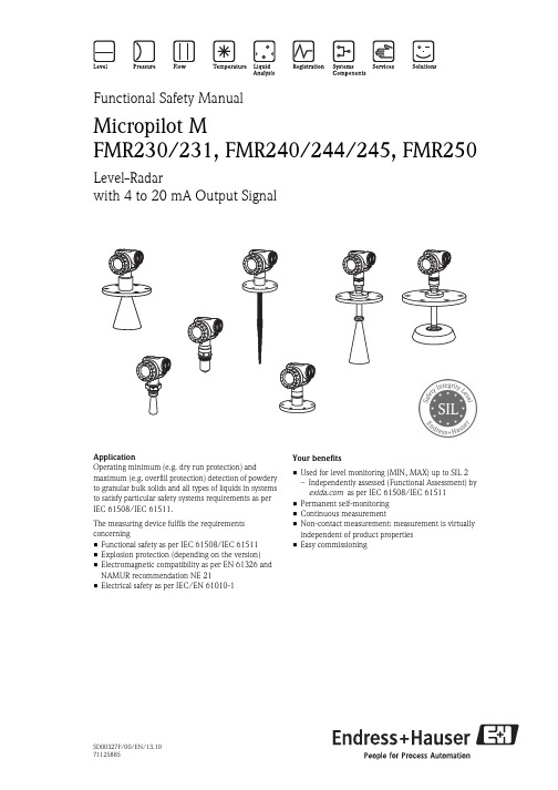
SD00327F/00/EN/13.1071125885Functional Safety ManualMicropilot MFMR230/231, FMR240/244/245, FMR250Level-Radarwith 4 to 20 mA Output SignalApplicationOperating minimum (e.g. dry run protection) andmaximum (e.g. overfill protection) detection of powdery to granular bulk solids and all types of liquids in systems to satisfy particular safety systems requirements as per IEC 61508/IEC 61511.The measuring device fulfils the requirements concerning•Functional safety as per IEC 61508/IEC 61511•Explosion protection (depending on the version)•Electromagnetic compatibility as per EN 61326 and NAMUR recommendation NE 21•Electrical safety as per IEC/EN 61010-1Your benefits•Used for level monitoring (MIN, MAX) up to SIL 2–Independently assessed (Functional Assessment) by as per IEC 61508/IEC 61511•Permanent self-monitoring •Continuous measurement•Non-contact measurement: measurement is virtually independent of product properties •Easy commissioningMicropilot M Table of contentsSIL Declaration of Conformity. . . . . . . . . . . . . . . . . . .3Introduction. . . . . . . . . . . . . . . . . . . . . . . . . . . . . . . . .4Structure of the measuring system. . . . . . . . . . . . . . . .4System components . . . . . . . . . . . . . . . . . . . . . . . . . . . . . . . . . . . 4Description of use as a protective system . . . . . . . . . . . . . . . . . . . . 5Permitted device types . . . . . . . . . . . . . . . . . . . . . . . . . . . . . . . . . 5Supplementary device documentation . . . . . . . . . . . . . . . . . . . . . . 7Description of the safety requirements andboundary conditions . . . . . . . . . . . . . . . . . . . . . . . . . .8Safety function . . . . . . . . . . . . . . . . . . . . . . . . . . . . . . . . . . . . . . . 8Restrictions for use in safety-related applications . . . . . . . . . . . . . . 8Functional safety indicators . . . . . . . . . . . . . . . . . . . . . . . . . . . . . . 9Behavior of device during operation and in case of error . . . . . . . 11Installation . . . . . . . . . . . . . . . . . . . . . . . . . . . . . . . . . . . . . . . . . 11Operation . . . . . . . . . . . . . . . . . . . . . . . . . . . . . . . . . . . . . . . . . . 11Maintenance . . . . . . . . . . . . . . . . . . . . . . . . . . . . . . . . . . . . . . . 14Proof-test. . . . . . . . . . . . . . . . . . . . . . . . . . . . . . . . . .15Proof-test . . . . . . . . . . . . . . . . . . . . . . . . . . . . . . . . . . . . . . . . . . 15Process for proof-testing . . . . . . . . . . . . . . . . . . . . . . . . . . . . . . . 15Repairs. . . . . . . . . . . . . . . . . . . . . . . . . . . . . . . . . . . .16Repairs . . . . . . . . . . . . . . . . . . . . . . . . . . . . . . . . . . . . . . . . . . . . 16Appendix. . . . . . . . . . . . . . . . . . . . . . . . . . . . . . . . . .17Commissioning or proof test protocol . . . . . . . . . . . . . . . . . . . . . 17Exida Management Summary . . . . . . . . . . . . . . . . . .182Endress+HauserMicropilot MEndress+Hauser 3SIL Declaration of ConformitySIL_08006a_deMicropilot M4Endress+HauserIntroduction!Note!General information on functional safety (SIL) is available at:/SIL (German) or /SIL (English) and in Competence Brochure CP002Z "Functional Safety in the Process Industry - Risk Reduction with Safety Instrumented Systems".Structure of the measuring systemSystem componentsThe measuring system's devices are displayed in the following diagram (example).An analog signal (4 to 20 mA) in proportion to the level is generated in the transmitter. This is sent to adownstream logic unit (e.g. PLC, limit signal transmitter, etc.) where it is monitored to determine whether it is below or above a specified limit value.For fault monitoring, the logic unit must recognize both HI-alarms (≥ 21.0 mA) and LO-alarms (≤ 3.6 mA).Micropilot MEndress+Hauser 5Description of use as a protective systemThe Micropilot M is a "downward-looking" measuring system that functions according to the ToF method (ToF = Time of Flight). The distance from the reference point (process connection of the measuring device) to the product surface is measured. Radar impulses are emitted by an antenna, reflected off the product surface and received again by the radar system.Typical measuring arrangement:!Note!Correct installation is a prerequisite for safe operation of the device.Permitted device typesThe details pertaining to functional safety in this manual relate to the device versions listed below and are valid as of the specified software and hardware version. Unless otherwise specified, all subsequent versions can also be used for safety instrumented systems.A modification process according to IEC 61508 is applied for device changes.Valid device versions for safety-related use:Micropilot M FMR230, FMR244FeatureDesignation Version 010Approval all 020Antennaall 030Antenna Seal; Temperature all 040Process Connection all 050Output; Operation A, B, K 060Housing all 070Cable Entry all 080Additional OptionallValid software version: FMR230: as of 01.04.00; FMR244: as of 01.05.00Valid hardware version (electronics): as of delivery date January 2010Micropilot MMicropilot M FMR231Feature Designation Version010Approval all020Antenna; Inactive Length all030Process Connection all040Output; Operation A, B, K050Housing all060Cable Entry all070Gas-Tight Feed Through all080Additional Option allValid software version: FMR231: as of 01.04.00Valid hardware version (electronics): as of delivery date January 2010Micropilot M FMR240, FMR250Feature Designation Version010Approval all020Antenna all030Antenna Seal; Temperature all040Antenna Extension all050Process Connection all060Output; Operation A, B, K070Housing all080Cable Entry all090Additional Option allValid software version: FMR240, FMR250: as of 01.05.00Valid hardware version (electronics): as of delivery date January 2010Micropilot M FMR245Feature Designation Version010Approval all020Antenna all030Process Connection all040Output; Operation A, B, K050Housing all060Cable Entry all070Additional Option allValid software version: FMR245: as of 01.05.00Valid hardware version (electronics): as of delivery date January 20106Endress+HauserMicropilot MEndress+Hauser 7Supplementary device documentationDocumentationContentsCommentTechnical InformationTI00345F/00 (FMR23x, FMR24x)TI00390F/00 (FMR250)–Technical data–Instructions on accessories –The documentation is available on the Internet.→ .Operating Instructions (HART)BA00218F/00 (FMR230)BA00219F/00 (FMR231)BA00220F/00 (FMR240)BA00248F/00 (FMR244)BA00251F/00 (FMR245)BA00284F/00 (FMR250)–Identification –Installation –Wiring –Operation–Commissioning –Maintenance –Accessories –Troubleshooting –Technical data –Appendix–The documentation is supplied with the device.–The documentation is also available on the Internet.→ .Operating Instructions (Device Functions)BA00221F/00 (FMR23x)BA00291F/00 (FMR24x, FMR250)–Instructions on use–Micropilot M function menu –Function groups ...–...–Envelope curve –Troubleshooting–Function menu index–The documentation is available on the Internet.→ .Safety instructions depending on the selected version "Approval"–Safety, installation and operating instructions for devices, which are suitable for use in potentially explosive atmospheres or as overfill protection (WHG, German Water Resources Act).Additional safety instructions(XA, XB, XC, ZE, ZD) are supplied with certified device versions.Please refer to the nameplate for the relevant safety instructions.Micropilot M8Endress+HauserDescription of the safety requirements and boundary conditionsSafety functionThe mandatory settings and safety function data emanate from the descriptions from →ä11.The measuring system's reaction time is ≤ 5 s.!Note!MTTR is set at 8 hours.Safety-related signal:The Micropilot M's safety-related signal is the 4 to 20 mA analog output signal. All safety measures refer to this signal exclusively.The Micropilot M additionally communicates effectively via HART and contains all HART features with additional device information.The safety-related output signal is fed to a downstream logic unit, e.g. a programmable logic controller or a limit signal transmitter where it is monitored for the following:–Overshooting and/or undershooting a specified level limit.–The occurrence of a fault, e.g. error current (≤ 3.6 mA, ≥ 21.0 mA, interruption or short-circuit of the signal line).Restrictions for use in safety-related applicationsThe measuring system must be used correctly for the specific application, taking into account the medium properties and ambient conditions. Carefully follow instructions pertaining to critical process situations and installation conditions from the Operating Instructions.The specifications from the Operating Instructions (→ä7, "Supplementary device documentation") must not be exceeded.The following restriction also applies to safety-related use:–The accuracy of the 4 to 20 mA safety-related output signal is ± 10%.Micropilot MFunctional safety indicators The following tables show specific indicators for functional safety.Characteristic as per IEC 61508FMR23x with 4 to 20 mA outputSafety functions MIN MAXSIL2HFT0Device type BMode of operation Low demand modeSFF 67 % 74 %MTTR8 hRecommended time interval for proof-testing T1 1 yearλsd *2 392 FIT 87 FITλsu *2951 FIT1125 FITλdd *2541 FIT846 FITλdu *2916 FIT710 FITλtot *32800 FIT2768 FITPFD avg for T1 = 1 year *14,01 × 10-33,11 × 10-3PFD avg for T1 = 1 year *54,75 × 10-33,69 × 10-3MTBF *335 yearsSystem reaction time *4≤ 5 s*1 PFD avg*2 According to Siemens SN29500.*3 According to Siemens SN29500, including faults outside the safety function.*4 Step response time as per DIN EN 61298-2.*5 Calculated, with MTTR = 24 h, lifetime (LT) = 10 years and proof test coverage (PTC) = 98 %,Proof-test intervalEndress+Hauser9Micropilot MCharacteristic as per IEC 61508FMR24x, FMR250 with 4...20 mA outputSafety functions MIN MAXSIL2HFT0Device type BMode of operation Low demand modeSFF 68 % 75 %MTTR8 hRecommended time interval for proof-testing T1 1 yearλsd *2 356 FIT 99 FITλsu *21031 FIT1207 FITλdd *2621 FIT878 FITλdu *2903 FIT697 FITλtot *32911 FIT2881 FITPFD avg for T1 = 1 year *13,96 × 10-33,05 × 10-3PFD avg for T1 = 1 year *54,68 × 10-33,62 × 10-3MTBF *335 yearsSystem reaction time *4≤ 5 s*1 PFD avg*2 According to Siemens SN29500.*3 According to Siemens SN29500, including faults outside the safety function.*4 Step response time as per DIN EN 61298-2.*5 Calculated, with MTTR = 24 h, lifetime (LT) = 10 years and proof test coverage (PTC) = 98 %,Proof-test interval10Endress+HauserDangerous undetected failures in this scenario:An incorrect output signal that deviates from the real measured value by more than 10%, but is still in the range of 4 to 20 mA, is considered a dangerous, undetected failure.Useful lifetime of electrical components:The established failure rates of electrical components apply within the useful lifetime as per IEC 61508:2000, section 7.4.7.4. note 3.Behavior of device during operation and in case of error Behavior of device during power-upThe safe 4 to 20 mA output signal is available after 17 s after the device is switched on or when the voltage returns.Device response in the event of alarms or warningsError currentIn the event of an alarm, the output current can be configured to a value of ≤ 3.6 mA or ≥ 21.0 mA.In some cases (e.g. failure of power supply, a cable open circuit and faults in the current output itself, where the error current ≥ 21.0 mA cannot be set), output currents ≤ 3.6 mA irrespective of the configured error current can occur.For alarm monitoring, the logic unit must therefore be able to recognize both HI-alarms (≥ 21.0 mA) and LO-alarms (≤ 3.6 mA).Alarm and warning messagesAdditional information is available in the form of fault codes on the alarm and warning messages output.Installation Installation, wiring and commissioningInstallation, wiring and commissioning of the device is described in the accompanying Operating Instructions(→ä7, "Supplementary device documentation").OrientationThe permitted orientations of the device are described in the Operating Instructions.Operation Calibration of the measuring pointCalibration of the measuring point is described in the Operating Instructions.The method of device configuration!Note!Altered settings (display/FieldCare) in the "extended calibr." function group (Pos. 05) such as "offset" or"curr.turn down" (Pos. 063) in the "output" function group have an effect on the output signal.This must be taken into account when calculating the response height (see relevant Operating Instructions).We recommend that you check that the behavior of the current signal matches the expected behavior by meansof level simulation (correctness of configuration).Configuration schemata/basic calibrationThe parameters are safety-oriented with the "WHG" setting in 018 (→ information in the following table).As an alternative to activating the "WHG" setting, it is also possible to make the safety-oriented setting manually. In doing so, please observe the information in the table below.!Note!The parameters in italics are located on the service level, which can be opened with the code "300".FieldCare / Display - plain text displayDisplay VU331 Position Media type (only FMR24x, FMR250 (software version 01.05.00))001↓Tank shape *1 (FMR23x, FMR24x) or Bin type (FMR250)002↓Medium property003↓Process conditions004↓Empty calibration E005↓Full calibration F006↓Pipe diameter (for bypass / stilling well)007↓MappingSee Operating Instructions ↓Further settings: function group 05See Operating Instructions ↓Overfill protection WHG018↓On-site locking: 3 keys on the VU331 displayYes *1 For FMR 240 with wave guide antenna, stilling well must always be selected as tank shape.FieldCare /Display - plain text display Value/parameterDisplay VU331CommentSafety settings Output on ALARM Max. 110 %, 22 mA 010Parameter must be configured in this way Output echo loss ALARM 012Parameter must be configured in this way Delay time1 s014→ Note 1In safety distance SD self holding016→ Note 3!Note! 1.This parameter determines the reaction time of the device in the event of echo loss; a setting of less than 30 s is recommended.2.This parameter determines the reaction time of the device; deviating settings are possible.In case of changes in "process cond." (004) it is automatically adjusted. The corresponding reaction time is indicated in the documentation BA.3.This parameter can be selected differently, depending on the application.A measuring condition (echo) which results in an ALARM in the "Safety distance SD" area can be reset or deleted by–confirming the ALARM in Pos. 017 locally by means of the VU331 LCD display;–confirming the alarm via the communication protocol (HART) (FieldCare: "ackn. alarm" under safety settings).FieldCare /Display - plain text display Value/parameterDisplay VU331CommentFiltering/averaging/delay Envelope statistics up 20D23→ Note 2Envelope statistics down 20D24→ Note 2MAM filter length 50D11→ Note 2MAM filter border 10D12→ Note 2Output damping 0058→ Note 2Echo detection FEF edge (nur bei MIN)00D56Parameter must be configured in this way FAC mode FMC rising 0D99Parameter must be configured in this way FAC adder6 dB 0D35Parameter must be configured in this way Tank bottom detection OFF0D61Parameter must be configured in this way First echo factor unchanged, but if previously smaller than 30, than: 0D530D51→ Note 3FEF threshold 00D52→ Note 3FEF at near distance 30 dB 0D53→ Note 3FEF distance near 500 mm 0D54→ Note 3FEF distance far 3000 mm0D55Parameter must be configured in this way Max. filling speed 0 mm/s (factory setting)0D15Parameter must be configured in this way Max. drain speed 0 mm/s (factory setting)0D16Parameter must be configured in this wayOtherDetection window OFF0A7Parameter must be configured in this way Hysterese width 0 mm (factory setting)0D14Parameter must be configured in this way Communication address 0060Parameter must be configured in this way Current output mode "Standard" if previously "Fixed current" 063Parameter must be configured in this way SimulationSim. / OFF065Parameter must be configured in this wayLockingThe device must be locked once the Micropilot M has been calibrated as per the Operating Instructions.Type of locking Code/action Position/VU331 displayHardware (recommended) 3 keys together "lock"Locally via VU331 display (keys O and S and F)↓Software (mandatory)WHG (german)018UnlockingThe device is unlocked by firstly removing the hardware lock by locally pressing all the three keys together viathe VU331 LCD display and then by setting the "Overfill protection" parameter (Position 018) to "Standard" ifnecessary.Type of unlocking Code/action Position/VU331 displayHardware (if locked) 3 keys together "unlock"Locally via VU331 display (keys O and S and F)↓Software Standard018Maintenance Please refer to the relevant Operating Instructions (→ä7, "Supplementary device documentation") forinstructions on maintenance and recalibration.Alternative monitoring measures must be taken to ensure process safety during configuration, proof-testing andmaintenance work on the device.Proof-testProof-test Check the operativeness and safety of safety functions at appropriate intervals!The operator must determine the time intervals.You can refer to the diagram "Proof-test interval" →ä9, →ä10, for this purpose.Proof-testing of the device can be performed as follows:–Approaching the level (→ test sequence A).–Removing the device and measuring a medium with comparable properties (→ test sequence B).You must also check that all cover seals and cable entries are sealing correctly.Process for proof-testing Test sequence APreparation1.Connect suitable measuring device (recommended accuracy better ±0.1 mA) to the current output.2.Determine the safety setting (level limit monitoring).Procedure for level limit monitoring1.Approach the level directly below (MAX monitoring) or directly above (MIN monitoring) the level limitto be monitored.2.Read the output current, record it and assess for accuracy.3.Approach the level directly above (MAX monitoring) or directly below (MIN monitoring) the level limitto be monitored.4.Read the output current, record it and assess for accuracy.5.The test is deemed successful if the current in step 2 does not result in activation of the safety functionbut the current in step 4 does.!Note!The proof-test is deemed to have failed if the expected current value deviates for a specific level by >±10%.For troubleshooting, → Operating Instructions (→ä7, "Supplementary device documentation"), Section 9.98% of dangerous, undetected failures are detected using this test.Test sequence BPreparation1.Prepare the test tank with the medium (dielectric constant comparable to that of the medium to bemeasured).For installation instructions, → Operating Instructions (→ä7, "Supplementary devicedocumentation"), Section 3.2.Remove the device and mount it in the test tank.3.Perform interference echo mapping if the shape and size of the test tank is different.4.Connect suitable measuring device (recommended accuracy better than ±0.1 mA) to the current output.5.Determine the safety setting (level limit monitoring).Procedure for level limit monitoring→ Test sequence A!Note!The proof-test is deemed to have failed if the expected current value deviates for a specific level by > ±10%.For troubleshooting, → Operating Instructions (→ä7, "Supplementary device documentation"), Section 9.98% of dangerous, undetected failures are detected using this test."Caution!If an interference echo mapping was performed in the test tank, a valid interference echo mapping must beperformed after the device is mounted in the original tank.!Note!If one of the test criteria from the test sequences described above is not fulfilled, the device may no longer beused as part of a safety instrumented system.The purpose of proof-testing is to detect random device failures. The impact of systematic faults on the safetyfunction is not covered by this test and must be assessed separately.Systematic faults can be caused, for example, by process material properties, operating conditions, build-up orcorrosion.RepairsRepairs Repairs on the devices must always be carried out by Endress+Hauser.Safety functions cannot be guaranteed if repairs are carried out by anybody else.Exception:The following components can be replaced by the customer if the person responsible for doing so has beentrained beforehand by Endress+Hauser:–Sensor–HF module–Electronic insert–Terminal moduleThe replaced components must be sent to Endress+Hauser for the purpose of fault analysis.Once the components have been replaced, a proof-test must be carried out as per test sequence A (→ä15)or test sequence B (→ä15).In the event of failure of a SIL-labeled Endress+Hauser device, which has been operated in a protectionfunction, the "Declaration of Contamination and Cleaning" with the corresponding note "Used as SIL device inprotection system" must be enclosed when the defective device is returned.Please refer to the Section "Return" in the Operating Instructions (→ä7, "Supplementary devicedocumentation").AppendixCommissioning or proof test ArrayprotocolExida Management SummaryEndress+Hauser2122Endress+HauserEndress+Hauser23Instruments InternationalEndress+HauserInstruments International AGKaegenstrasse 24153 ReinachSwitzerlandTel.+41 61 715 81 00Fax+41 61 715 25 00***************.comSD00327F/00/EN/13.1071125885FM+SGML 6.071125885。
FC4中文资料

Fusible CarbonFilm ResistorsFC4•Predictable fusing characteristics •Constant voltage fusing characteristics •Fuses at very low powers •Flame retardant lacquerFC4Power rating at 70°C watts 0.33Resistance range ohms 1R0-5K1TCRppm/°C300Resistance tolerance %5, 10Standard values E24 preferredThermal impedance °C/watt215Ambient temperature range°C -55 to 125General NoteWelwyn Components reserves the right to make changes in product specification without notice or liability. All information is subject to Welwyn’s own data and is considered accurate at time of going to print.© Welwyn Components Limited · Bedlington, Northumberland NE22 7AA, UKTelephone: +44 (0)1670 822181 · Facsimile: +44 (0)1670 829465 · Email: info@ · Website: Electrical DataIssue B · 03.02A subsidiary of TT electronics plc Welwyn Components166ConstructionThe carbon film is deposited on a high purity ceramic rod.End caps are fitted and termination wires welded to the caps.The resistive film is adjusted to the required value by a special helical cut; finally the flame retardant lacquer protection is applied to the resistor body and marked with an indelible ink.TerminationsMaterial Solder-coated copper wire.StrengthThe terminations meet the requirements of IEC 68.2.21Solderability The terminations meet the requirements ofIEC 115-1, Clause 4.17.3.2MarkingResistance value and tolerances are identified in accordance with IEC62.4 - band colour code. A fifth (yellow) band denotes that the product is fusible and suitable for use in constant voltage applications.Solvent ResistanceThe body protection and marking are resistant to all normal industrial cleaning solvents suitable for printed circuits.FlammabilityThe resistor coating will not burn or emit incandescent particles under any condition of applied temperature or power overload.Dimensions (mm) & Weight (g)PCB Min.mounting bend Type L Max D Max f min d nom centres radius Wt.nom FC46.22.521.00.610.20.60.3Physical DataL DfdFusible Carbon Film ResistorFC4© Welwyn Components Limited Bedlington, Northumberland NE22 7AA, UKTelephone: +44 (0)1670 822181 · Facsimile: +44 (0)1670 829465 · Email: info@ · Website: Issue B · 03.02Welwyn Components167PackagingAll FC resistors are supplied tape packed ready for loading on to automatic sequencing and insertion ponent wires will not protrude beyond the outside edge of the tapes.Lead formed resistors can also be supplied. Standardoptions of Lancet, Radial and Goalpost forming are shown in Lead Form Information section.Alternative packaging available by request.52f 1f 2665Body location f 1 – f 2 ≤ 1.4 mmGRAPH 1 FUSING CHARACTERISTICS (constant voltage)F u s i n g t i m e (s e c o n d s )Applied power (watts)0.13.5510150.51.02.05.01020304050100GRAPH 2 MAXIMUM FUSING VOLTAGEM a x i m u m p e r m i s s a b l e a p p l i e d v o l t a g eResistance value (ohms)1101001k300280260240220200180160140120100806040200Maximum1.0 - 1k ∆R%0.2Load 1000 hrs at 70°C>1k to 5.1k0.8Derating from rated power at 70°C zero at 125°CClimatic ∆R%0.5Climatic category 40/125/56Temperature rapid change ∆R%0.25Resistance to solder heat ∆R%0.5Vibration and bump ∆R%0.1Isolation resistanceohms >1GPerformance DataType FC4Ammo pack5000Standard Quantities Per PackageGraph 1Fusing Characteristics (constant voltage)Graph 2Maximum Fusing Voltage。
FCN-244M中文资料
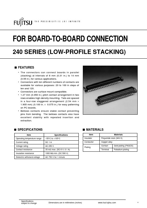
s SPECIFICATIONS
Item Operating temperature range Current rating Voltage rating Contact resistance Insulation resistance Dielectric withstand voltage
Specifications –55°C to +105°C DC 1 A AC 250 V 35 mΩ max. (DC 6 V, 0.1 A) 1000 MΩ min. (DC 500 V) AC 750 V for 1 minute
Connectors with board lock brackets are also available. Specify a part number by replacing -G/0 at the end with -G/A.
Specifications
subject to change
Dimensions are in millimeters (inches)
TTP-244 TTP-244 Plus 熱感式 熱轉式條碼印表機 说明书

目錄一、產品簡介 (1)1.1安規認證 (1)二、入門 (2)2.1拆封及清點配件 (2)2.2印表機組件 (3)2.3外部紙卷架(選購配備) (8)2.4按鍵及指示燈 (9)三、安裝 (10)3.1安裝條碼印表機 (10)3.2安裝標籤紙及吊牌 (10)3.3裝設熱轉印碳帶 (13)3.4外部紙卷架的安裝(選購配備) (16)3.5自測模式 (17)3.6除錯模式(D UMP M ODE) (17)3.7安裝SD記憶卡(僅TTP-244P LUS機種有此選購功能) (19)四、使用 (21)4.1開機功能設定 (21)4.1.1 自我測試功能 (21)4.1.2 間隙感應器靈敏度的校正 (21)4.1.3 印表機初始化 (Initialization) (22)4.2故障排除 (23)五、印表機之簡易保養程序 (24)5.1清潔印字頭 (25)5.2印表機上蓋、外殼及標籤出口之清潔 (26)5.3清潔印表機內部之其他機構 (26)警示:安全指示說明 (27)一、產品簡介感謝您購買本公司製造的標籤印表機。
此輕巧的桌上型印表機將以經濟的價位提供您優越的列印品質。
此印表機功能強大且使用簡便,是同級熱感、熱轉印表機中的最佳選擇。
此印表機提供熱感、熱轉兩種列印方式。
列印速度可調整在每秒2, 3 或 4吋。
可接受多種標籤及紙張,包括卷裝紙,摺頁式標籤紙等。
最常用的條碼格式均可列印。
可以將字型及條碼旋轉 4 種角度。
且提供 8 組不同大小的英數字體。
應用放大功能,字體尺寸可作更大範圍的變化。
平滑字型可從易用的標籤設計視窗軟體中下載。
此外,內建BASIC解譯器,可獨立執行 BASIC 程式功能,包括數值運算、邏輯運算、迴圈、流程控制及檔案管理。
善用印表機的程式功能可大幅提昇標籤印製的效率。
印表機狀態及錯誤訊息可經由印表機印出或經由連接埠顯示於終端機上。
1.1 安規認證CE Class A, FCC Class A, TÜV/Safety, CCC警告1. 手指及身體其他部位請遠離裁刀模組中危險可動部位2. 主機板中包含的計時器電池CR2032如果更換不正確會有爆炸的危險3. 請依製造商說明書處理用過之電池二、入門本印表機業經特殊包裝以抵抗運輸途中可能產生的損害。
天诚通信-铜产品培训资料

目录超五类非屏蔽信息(xìnxī)模块 (5)超五类非屏蔽(píngbì)直通信息模块..................................................................................... 错误!未定义书签。
超五类屏蔽信息(xìnxī)模块 (6)超五类屏蔽直通信息(xìnxī)模块........................................................................................... 错误!未定义书签。
六类非屏蔽信息(xìnxī)模块 (7)六类屏蔽信息模块 (8)超六类非屏蔽信息模块 (9)超六类非屏蔽信息模块 (10)超六类屏蔽信息模块 (10)超五类非屏蔽免打线水晶头 .................................................................................................... 错误!未定义书签。
经典系列平口面板 . (12)雅典系列平口面板 (13)雅典系列斜口面板 (14)雅典系列有线电视面板 (15)数据语音电视三合一面板 (16)二位方形光纤开起式地脚插座 (17)三位方形信息弹起式地脚插座 (18)三位圆形信息弹起式地脚插座 (19)三位方形信息开起式地脚插座 (20)三位圆形信息开起式地脚插座 (21)五孔方形弹起式电源插座 (22)五孔圆形弹起式电源插座 (23)六孔方形弹起式电源插座 (24)六位桌面型地脚插座 (25)地插功能配件 (26)24口非屏蔽空配线架 (28)24口非屏蔽空配线架〔带防尘门〕 (29)24口超五类非屏蔽配线架 (30)24口超五类非屏蔽角型配线架................................................................................................ 错误!未定义书签。
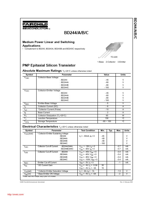
BD244资料
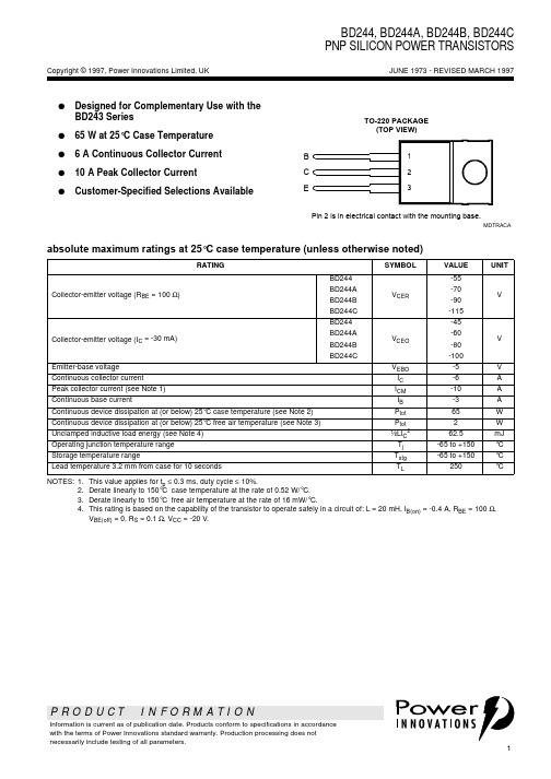
BD244, BD244A, BD244B, BD244C PNP SILICON POWER TRANSISTORS2JUNE 1973 - REVISED MARCH 1997P R O D U C T I N F O R M A T I O NNOTES:5.These parameters must be measured using pulse techniques, t p = 300 µs, duty cycle ≤ 2%.6.These parameters must be measured using voltage-sensing contacts, separate from the current carrying contacts.†Voltage and current values shown are nominal; exact values vary slightly with transistor parameters.electrical characteristics at 25°C case temperaturePARAMETER TEST CONDITIONSMIN TYPMAXUNITV (BR)CEOCollector-emitter breakdown voltageI C = -30 mA (see Note 5)I B = 0BD244BD244A BD244B BD244C -45-60-80-100VI CESCollector-emitter cut-off current V CE = -55 VV CE = -70 V V CE = -90 V V CE =-115 VV BE =0V BE =0V BE =0V BE =0BD244BD244A BD244B BD244C -0.4-0.4-0.4-0.4mA I CEO Collector cut-off current V CE = -30 V V CE = -60 V I B =0I B =0BD244/244A BD244B/244C-0.7-0.7mA I EBO Emitter cut-off current V EB = -5 V I C =0-1mA h FE Forward current transfer ratio V CE = -4 V V CE = -4 V I C =-0.3A I C = -3A (see Notes 5 and 6)3015V CE(sat)Collector-emitter saturation voltage I B = -1 A I C = -6A (see Notes 5 and 6)-1.5V V BE Base-emitter voltageV CE = -4 V I C = -6 A (see Notes 5 and 6)-2Vh feSmall signal forward current transfer ratio V CE = -10 V I C =-0.5A f = 1 kHz 20|h fe |Small signal forward current transfer ratioV CE = -10 VI C =-0.5Af = 1 MHz3thermal characteristicsPARAMETERMINTYPMAX UNIT R θJC Junction to case thermal resistance 1.92°C/W R θJAJunction to free air thermal resistance62.5°C/Wresistive-load-switching characteristics at 25°C case temperaturePARAMETERTEST CONDITIONS †MIN TYP MAX UNIT t on T urn-on time I C = -1 A V BE(off) = 3.7 VI B(on) = -0.1 A R L = 20 ΩI B(off) = 0.1 A t p = 20 µs, dc ≤ 2%0.3µs t offT urn-off time1µs3BD244, BD244A, BD244B, BD244C PNP SILICON POWER TRANSISTORS4JUNE 1973 - REVISED MARCH 1997P R O D U C T I N F O R M A T I O NMAXIMUM SAFE OPERATING REGIONSTHERMAL INFORMATION5BD244, BD244A, BD244B, BD244C PNP SILICON POWER TRANSISTORS6JUNE 1973 - REVISED MARCH 1997P R O D U C T I N F O R M A T I O NIMPORTANT NOTICEPower Innovations Limited (PI) reserves the right to make changes to its products or to discontinue any semiconductor product or service without notice, and advises its customers to verify, before placing orders, that the information being relied on is current.PI warrants performance of its semiconductor products to the specifications applicable at the time of sale in accordance with PI's standard warranty. Testing and other quality control techniques are utilized to the extent PI deems necessary to support this warranty. Specific testing of all parameters of each device is not necessarily performed, except as mandated by government requirements.PI accepts no liability for applications assistance, customer product design, software performance, or infringement of patents or services described herein. Nor is any license, either express or implied, granted under any patent right, copyright, design right, or other intellectual property right of PI covering or relating to any combination,machine, or process in which such semiconductor products or services might be or are used.PI SEMICONDUCTOR PRODUCTS ARE NOT DESIGNED, INTENDED, AUTHORIZED, OR WARRANTED TO BE SUIT ABLE FOR USE IN LIFE-SUPPORT APPLICA TIONS, DEVICES OR SYSTEMS.Copyright © 1997, Power Innovations Limited。
ESDR0502B中文资料(ONSEMI)中文数据手册「EasyDatasheet - 矽搜」
MILLIMETERS
DIM MIN NOM MAX
ቤተ መጻሕፍቲ ባይዱ
A 0.70 0.80 0.90
A1 0.00 0.05 0.10
b 0.15 0.20 0.30
C 0.10 0.15 0.25
D 1.55 1.60 1.65
E 0.70 0.80 0.90
芯片中文手册,看全文,戳
ESDR0502B
瞬态电压抑制器
ESD保护二极管与超低
电容
该ESDR0502B旨在保护电压敏感
从因损坏部件的ESD在需要超低电容,以保持信号完整性应用.优良钳位能力,
低泄漏和快速响应时间相结合,与0.5 pF的超低二极管电容由于ESD提供
最好在从集成电路损坏类保护.小型SC-75封装,非常适合设计电路板空间非
芯片中文手册,看全文,戳
ESDR0502B
电气特性
(TA = 25°C除非另有说明)
符
参数
IPP
最大反向峰值脉冲电流
VC
钳位电压@ I
PP
VRWM IR
工作峰值反向电压
最大反向漏电流用V
RWM
VBR
击穿电压@我
T
IT
测试电流
IF
正向电流
VF
正向电压@我
F
Ppk
峰值功率耗散
C
电容用V
参见应用笔记AND8308 / D的生存能力规范的进一步说明.
3 12
SC−75 CASE 463 方式4
标记 框图
AD中号G G
1
AD
=器件代码
M
=日期代码*
BF244B中文资料
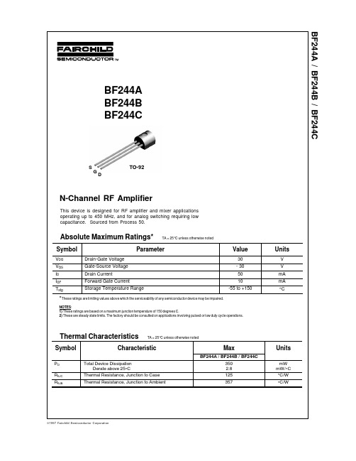
= -1.5V 5 10
20 10 -1
VGS(OFF)
@ V GS = 15V, I D= 1nA
3 2 1 - 10
0.05 0.1 0.2 0.5 1 2 I D -- DRAIN CURRENT (mA)
-2 -3 -5 -7 V - GATE-SOURCE VOLTAGE(V)
GS
Transconductance vs Drain Current
gfs -- TRANSCONDUCTANCE (mmhos) 10 e n- NOISE VOLTAGE ( nV/
Noise Voltage vs Frequency
V DG = 15V BW = 6.0 Hz @ f = 10 Hz, 100 Hz = 0.2 f @ f > 1.0 kHz
Hz )
O
O
8
50 30 20 10
4
V DS
= 100mV
-2.5 V
0 0 -1 -2 -3 -4 VGS - GATE-SOURCE VOLTAGE(V) -5
LM2445中文资料
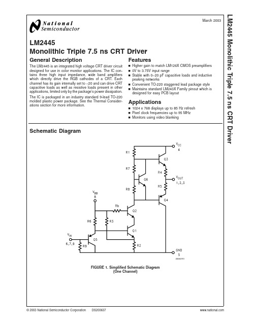
LM2445Monolithic Triple 7.5ns CRT DriverGeneral DescriptionThe LM2445is an integrated high voltage CRT driver circuit designed for use in color monitor applications.The IC con-tains three high input impedance,wide band amplifiers which directly drive the RGB cathodes of a CRT.Each channel has its gain internally set to −20and can drive CRT capacitive loads as well as resistive loads present in other applications,limited only by the package’s power dissipation.The IC is packaged in an industry standard 9-lead TO-220molded plastic power package.See the Thermal Consider-ations section for more information.Featuresn Higher gain to match LM126X CMOS preamplifiers n 0V to 3.75V input rangen Stable with 0–20pF capacitive loads and inductive peaking networksn Convenient TO-220staggered lead package style n Maintains standard LM243X Family pinout which is designed for easy PCB layoutApplicationsn 1024x 768displays up to 85Hz refresh n Pixel clock frequencies up to 95MHz n Monitors using video blankingSchematic Diagram20063701FIGURE 1.Simplified Schematic Diagram(One Channel)March 2003LM2445Monolithic Triple 7.5ns CRT Driver©2003National Semiconductor Corporation Connection Diagram20063702Note:Tab is at GNDTop ViewOrder Number LM2445TAL M 2445 2Absolute Maximum Ratings(Notes1, 3)If Military/Aerospace specified devices are required, please contact the National Semiconductor Sales Office/ Distributors for availability and specifications.Supply Voltage(V CC)+90V Bias Voltage(V BB)+16V Input Voltage(V IN)0V to4.5V Storage Temperature Range(T STG)−65˚C to+150˚C Lead Temperature(Soldering,<10sec.)300˚CESD Tolerance,Human Body Model 2kVMachine Model250VOperating Ranges(Note2)V CC+60V to+85VV BB+8V to+15VV IN+0V to+3.75VV OUT+15V to+75VCase Temperature−20˚C to+100˚CDo not operate the part without a heat sink.Electrical Characteristics(See Figure2for Test Circuit)Unless otherwise noted:V CC=+80V,V BB=+12V,C L=8pF,T C=50˚C DC Tests:V IN= 2.25VDC AC Tests:Output=40V PP(25V-65V)at1MHzSymbol Parameter ConditionsLM2445Units Min Typical MaxI CC Supply Current All Three Channels,No Input Signal,No Output Load30mAI BB Bias Current All Three Channels18mAV OUT DC Output Voltage No AC Input Signal,V IN=1.25V626568V DCA V DC Voltage Gain No AC Input Signal−18−20−22∆A V Gain Matching(Note4),No AC Input Signal 1.0dBLE Linearity Error(Notes4,5),No AC Input Signal5%t R Rise Time(Note6),10%to90%7.5nst F Fall Time(Note6),90%to10%8nsOS Overshoot(Note6)1%Note1:Absolute Maximum Ratings indicate limits beyond which damage to the device may occur.Note2:Operating ratings indicate conditions for which the device is functional,but do not guarantee specific performance limits.For guaranteed specifications andtest conditions,see the Electrical Characteristics.The guaranteed specifications apply only for the test conditions listed.Some performance characteristics maychange when the device is not operated under the listed test conditions.Note3:All voltages are measured with respect to GND,unless otherwise specified.Note4:Calculated value from Voltage Gain test on each channel.Note5:Linearity Error is the variation in dc gain from V IN=1.0V to V IN=3.5V.Note6:Input from signal generator:t r,t f<1ns.LM24453AC Test CircuitFigure 2shows a typical test circuit for evaluation of the LM2445.This circuit is designed to allow testing of the LM2445in a 50Ωenvironment without the use of an expensive FET probe.The two 2490Ωresistors form a 200:1divider with the 50Ωresistor and the oscilloscope.A test point is included for easy use of an oscilloscope probe.The compensation capacitor is used to compensate the stray capacitance of the two 2490Ωresistors to achieve flat frequency response.20063703Note:8pF load includes parasitic capacitance.FIGURE 2.Test Circuit (One Channel)L M 2445 4Typical Performance Characteristics(VCC=+80V DC,V BB=+12V DC,C L=8pF,V OUT=40V PP (25V−65V),Test Circuit-Figure2unless otherwise specified)20063704 FIGURE3.V OUT vs V IN20063705 FIGURE4.Speed vs Temp.20063706 FIGURE5.LM2445Pulse Response20063707FIGURE6.Power Dissipation vs Frequency20063708FIGURE7.Speed vs Offset20063709FIGURE8.Speed vs Load CapacitanceLM24455Theory of OperationThe LM2445is a high voltage monolithic three channel CRT driver suitable for high resolution display applications.The LM2445operates with 80V and 12V power supplies.The part is housed in the industry standard 9-lead TO-220molded plastic power package.The circuit diagram of the LM2445is shown in Figure 1.The PNP emitter follower,Q5,provides input buffering.Q1and Q2form a fixed gain cascode amplifier with resistors R1and R2setting the gain at −20.Emitter followers Q3and Q4isolate the high output impedance of the cascode stage from the capacitance of the CRT cathode which decreases the sensitivity of the device to load capacitance.Q6provides biasing to the output emitter follower stage to reduce cross-over distortion at low signal levels.Figure 2shows a typical test circuit for evaluation of the LM2445.This circuit is designed to allow testing of the LM2445in a 50Ωenvironment without the use of an expen-sive FET probe.In this test circuit,the two 2.49k Ωresistors form a 200:1wideband,low capacitance probe when con-nected to a 50Ωcoaxial cable and a 50Ωload (such as a 50Ωoscilloscope input).The input signal from the generator is ac coupled to the base of Q5.Application HintsINTRODUCTIONNational Semiconductor (NSC)is committed to provide ap-plication information that assists our customers in obtaining the best performance possible from our products.The fol-lowing information is provided in order to support this com-mitment.The reader should be aware that the optimization of performance was done using a specific printed circuit board designed at NSC.Variations in performance can be realized due to physical changes in the printed circuit board and the application.Therefore,the designer should know that com-ponent value changes may be required in order to optimize performance in a given application.The values shown in this document can be used as a starting point for evaluation purposes.When working with high bandwidth circuits,good layout practices are also critical to achieving maximum per-formance.IMPORTANT INFORMATIONThe LM2445performance is targeted for the VGA (640x 480)to XGA (1024x 768,85Hz refresh)resolution market.The application circuits shown in this document to optimizeperformance and to protect against damage from CRT ar-cover are designed specifically for the LM2445.If another member of the LM246X family is used,please refer to its datasheet.POWER SUPPLY BYPASSSince the LM2445is a wide bandwidth amplifier,proper power supply bypassing is critical for optimum performance.Improper power supply bypassing can result in large over-shoot,ringing or oscillation.0.1µF capacitors should be connected from the supply pins,V CC and V BB ,to ground,as close to the LM2445as is practical.Additionally,a 47µF or larger electrolytic capacitor should be connected from both supply pins to ground reasonably close to the LM2445.ARC PROTECTIONDuring normal CRT operation,internal arcing may occasion-ally occur.Spark gaps,in the range of 200V,connected from the CRT cathodes to CRT ground will limit the maximum voltage,but to a value that is much higher than allowable on the LM2445.This fast,high voltage,high energy pulse can damage the LM2445output stage.The application circuit shown in Figure 9is designed to help clamp the voltage at the output of the LM2445to a safe level.The clamp diodes,D1and D2,should have a fast transient response,high peak current rating,low series impedance and low shunt capaci-tance.FDH400or equivalent diodes are recommended.Do not use 1N4148diodes for the clamp diodes.D1and D2should have short,low impedance connections to V CC and ground respectively.The cathode of D1should be located very close to a separately decoupled bypass capacitor (C3in Figure 9).The ground connection of D2and the decoupling capacitor should be very close to the LM2445ground.This will significantly reduce the high frequency voltage transients that the LM2445would be subjected to during an arcover condition.Resistor R2limits the arcover current that is seen by the diodes while R1limits the current into the LM2445as well as the voltage stress at the outputs of the device.R2should be a 1⁄2W solid carbon type resistor.R1can be a 1⁄4W metal or carbon film type resistor.Having large value resis-tors for R1and R2would be desirable,but this has the effect of increasing rise and fall times.Inductor L1is critical to reduce the initial high frequency voltage levels that the LM2445would be subjected to.The inductor will not only help protect the device but it will also help minimize rise and fall times as well as minimize EMI.For proper arc protection,it is important to not omit any of the arc protection compo-nents shown in Figure 9.L M 2445 6Application Hints(Continued)OPTIMIZING TRANSIENT RESPONSEReferring to Figure 9,there are three components (R1,R2and L1)that can be adjusted to optimize the transient re-sponse of the application circuit.Increasing the values of R1and R2will slow the circuit down while decreasing over-shoot.Increasing the value of L1will speed up the circuit as well as increase overshoot.It is very important to use induc-tors with very high self-resonant frequencies,preferably above 300MHz.Ferrite core inductors from ler Magnetics (part #78FR--k)were used for optimizing the performance of the device in the NSC application board.The values shown in Figure 11and Figure 12can be used as a good starting point for the evaluation of the ing variable resistors for R1and the parallel resistor will simplify finding the values needed for optimum performance in a given application.Once the optimum values are determined the variable resistors can be replaced with fixed values.EFFECT OF LOAD CAPACITANCEFigure 8shows the effect of increased load capacitance on the speed of the device.This demonstrates the importance of knowing the load capacitance in the application.EFFECT OF OFFSETFigure 7shows the variation in rise and fall times when the output offset of the device is varied from 40to 50V DC .The rise time shows a maximum variation relative to the center data point (45V DC )less than 5%.The fall time shows a variation of less than 8%relative to the center data point.THERMAL CONSIDERATIONSFigure 4shows the performance of the LM2445in the test circuit shown in Figure 2as a function of case temperature.The figure shows that the rise time of the LM2445increases by approximately 10%as the case temperature increases from 50˚C to 100˚C.This corresponds to a speed degrada-tion of 2%for every 10˚C rise in case temperature.The fall time increases by approximately 7%as the case tempera-ture increases from 50˚C to 100˚C.Figure 6shows the maximum power dissipation of the LM2445vs.Frequency when all three channels of the device are driving an 8pF load with a 40V p-p alternating one pixel on,one pixel off signal.The graph assumes a 72%active time (device operating at the specified frequency)which is typical in a monitor application.The other 28%of the time the device is assumed to be sitting at the black level (65V inthis case).This graph gives the designer the information needed to determine the heat sink requirement for his appli-cation.The designer should note that if the load capacitance is increased the AC component of the total power dissipation will also increase.The LM2445case temperature must be maintained below 100˚C.If the maximum expected ambient temperature inside the monitor is 70˚C and the power dissipation is 4.4W (from Figure 6,50MHz max.video frequency),then a maximum heat sink thermal resistance can be calculated:This example assumes a capacitive load of 8pF and no resistive load.TYPICAL APPLICATIONA typical application of the LM2445is shown in Figure 11and Figure ed in conjunction with an LM1267,a complete video channel from monitor input to CRT cathode can be achieved.Performance is ideal for 1024x 768resolution displays with pixel clock frequencies up to 95MHz.Figure 11and Figure 12are the schematic for the NSC demonstration board that can be used to evaluate the LM1267/2466com-bination in a monitor,and Figure 10shows the typical re-sponse at the red cathode for this application.The input video rise time is 3.2ns,and the peaking component values are those recommended in Figure 12.Table 1shows the typical cathode response of all three channels.20063710FIGURE 9.One Channel of the LM2445with the Recommended Application CircuitLM24457Application Hints(Continued)TABLE 1.LM2445Cathode Response Channel t r /OS t f /OS Red 6.3ns /7% 6.3ns /3%Green 6.1ns /6% 5.9ns /4%Blue6.5ns /3%6.4ns /2%PC BOARD LAYOUT CONSIDERATIONSFor optimum performance,an adequate ground plane,iso-lation between channels,good supply bypassing and mini-mizing unwanted feedback are necessary.Also,the length of the signal traces from the preamplifier to the LM2445and from the LM2445to the CRT cathode should be as short as possible.The following references are recommended:Ott,Henry W.,“Noise Reduction Techniques in Electronic Systems”,John Wiley &Sons,New York,1976.“Video Amplifier Design for Computer Monitors”,National Semiconductor Application Note 1013.Pease,Robert A.,“Troubleshooting Analog Circuits”,Butterworth-Heinemann,1991.Because of its high small signal bandwidth,the part may oscillate in a monitor if feedback occurs around the video channel through the chassis wiring.To prevent this,leads to the video amplifier input circuit should be shielded,and input circuit wiring should be spaced as far as possible from output circuit wiring.NSC DEMONSTRATION BOARDFigure 13shows the routing and component placement on the NSC LM1267/2466demonstration board.The schematic of the board is shown in Figure 11and Figure 12.This board provides a good example of a layout that can be used as a guide for future layouts.Note the location of the following components:•C19—V CC bypass capacitor,located very close to pin 4and ground pins•C20—V BB bypass capacitors,located close to pin 8and ground•C46,C47,C48—V CC bypass capacitors,near LM2445and V CC clamp diodes.Very important for arc protection.The routing of the LM2445outputs to the CRT is very critical to achieving optimum performance.Figure 14shows the routing and component placement from pin 1of the LM2445to the blue cathode.Note that the components are placed so that they almost line up from the output pin of the LM2445to the blue cathode pin of the CRT connector.This is done to minimize the length of the video path between these two components.Note also that D8,D9,R24and D6are placed to minimize the size of the video nodes that they are at-tached to.This minimizes parasitic capacitance in the video path and also enhances the effectiveness of the protection diodes.The anode of protection diode D8is connected directly to a section of the the ground plane that has a short and direct path to the LM2445ground pins.The cathode of D9is connected to V CC very close to decoupling capacitor C19(see Figure 14)which is connected to the same section of the ground plane as D8.The diode placement and routing is very important for minimizing the voltage stress on the LM2445during an arcover stly,notice that S3is placed very close to the blue cathode and is tied directly to CRT ground.20063716FIGURE 10.Red Cathode ResponseL M 2445 8A p p l i c a t i o n H i n t s(C o n t i n u e d )20063717F IG U R E 11.L M 126X /L M 246X D e m o n s t r a t i o n B o a r d S c h e m a t i cLM24459A p p l i c a t i o n H i n t s(C o n t i n u e d )20063718F IG U R E 12.L M 126X /L M 246X D e m o n s t r a t i o n B o a r d S c h e m a t i c (c o n t i n u e d )L M 244510元器件交易网LM2445 Application Hints(Continued)20063719FIGURE13.LM126X/LM246X Demo Board Layout11Application Hints(Continued)20063714FIGURE 14.Trace Routing and Component Placement for Blue Channel OutputL M 2445 12LM2445 Physical Dimensions inches(millimeters)unless otherwise noted ArrayCONTROLLING DIMENSION IS INCHVALUES IN[]ARE MILLIMETERSNS Package Number TA09AOrder Number LM2445TA13NotesLIFE SUPPORT POLICYNATIONAL’S PRODUCTS ARE NOT AUTHORIZED FOR USE AS CRITICAL COMPONENTS IN LIFE SUPPORT DEVICES OR SYSTEMS WITHOUT THE EXPRESS WRITTEN APPROVAL OF THE PRESIDENT AND GENERAL COUNSEL OF NATIONAL SEMICONDUCTOR CORPORATION.As used herein:1.Life support devices or systems are devices or systems which,(a)are intended for surgical implant into the body,or (b)support or sustain life,and whose failure to perform when properly used in accordance with instructions for use provided in the labeling,can be reasonably expected to result in a significant injury to the user.2.A critical component is any component of a life support device or system whose failure to perform can be reasonably expected to cause the failure of the life support device or system,or to affect its safety or effectiveness.National Semiconductor Americas Customer Support CenterEmail:new.feedback@ Tel:1-800-272-9959National SemiconductorEurope Customer Support CenterFax:+49(0)180-5308586Email:europe.support@Deutsch Tel:+49(0)6995086208English Tel:+44(0)8702402171Français Tel:+33(0)141918790National Semiconductor Asia Pacific Customer Support Center Fax:+65-62504466Email:ap.support@ Tel:+65-62544466National SemiconductorJapan Customer Support Center Fax:81-3-5639-7507Email:jpn.feedback@ Tel:81-3-5639-7560L M 2445M o n o l i t h i c T r i p l e 7.5n s C R T D r i v e rNational does not assume any responsibility for use of any circuitry described,no circuit patent licenses are implied and National reserves the right at any time without notice to change said circuitry and specifications.。
74贴片全系列

74贴片全系列下为74系列数字型号定义说明ACT-X 高性能CMOS逻辑门系列(输入TTL兼容具缓冲功能) AC-X 高性能CMOS逻辑门系列(具缓冲功能)ALS-X 高性能低功耗逻辑门系列(TTL兼容具缓冲功能)AS-X 高性能逻辑门系列(TTL兼容具缓冲功能)C-X CMOS逻辑门系列FCT-X 高速CMOS逻辑门系列F-X 高速逻辑门系列(TTL兼容)HC-4XX 高速COMS逻辑门系列(TTL兼容)HCT-4XX 高速COMS逻辑门系列(TTL兼容)HCTLS-XHCT-X 高速COMS逻辑门系列(TTL兼容)HCU-XHC-X 采用CMOS接口器的逻辑门系列LS-X 低功耗逻辑门系列(TTL兼容)S-X 高速逻辑门系列(TTL兼容)VHCT-X (TTL兼容有TTL接口器)MC101-XX 高速ECL逻辑门系列MC14-XXMC-XXCD4000-X 高速CMOS逻辑门系列(TTL兼容) 74-XX 逻辑门系列(XX表示序列号,例如74104 )75-XX系列注:能够提供样板的产品基本上都附有产品实物照片,请在选择购买的时候留意封装以及尺寸,样板一旦售出概不退换,谢谢合作.常用4000系列标准数字电路的中文名称资料型号器件名称厂牌备注CD4000 双3输入端或非门+单非门TICD4001 四2输入端或非门HIT/NSC/TI/GOLCD4002 双4输入端或非门NSCCD4006 18位串入/串出移位寄存器NSCCD4007 双互补对加反相器NSCCD4008 4位超前进位全加器NSCCD4009 六反相缓冲/变换器NSCCD4010 六同相缓冲/变换器NSCCD4011 四2输入端与非门HIT/TICD4012 双4输入端与非门NSCCD4013 双主-从D型触发器FSC/NSC/TOSCD4014 8位串入/并入-串出移位寄存器NSCCD4015 双4位串入/并出移位寄存器TICD4016 四传输门FSC/TICD4017 十进制计数/分配器FSC/TI/MOTCD4018 可预制1/N计数器NSC/MOTCD4019 四与或选择器PHICD4020 14级串行二进制计数/分频器FSCCD4021 08位串入/并入-串出移位寄存器PHI/NSCCD4022 八进制计数/分配器NSC/MOTCD4023 三3输入端与非门NSC/MOT/TICD4024 7级二进制串行计数/分频器NSC/MOT/TICD4025 三3输入端或非门NSC/MOT/TICD4026 十进制计数/7段译码器NSC/MOT/TICD4027 双J-K触发器NSC/MOT/TICD4028 BCD码十进制译码器NSC/MOT/TICD4029 可预置可逆计数器NSC/MOT/TICD4030 四异或门NSC/MOT/TI/GOLCD4031 64位串入/串出移位存储器NSC/MOT/TICD4032 三串行加法器NSC/TICD4033 十进制计数/7段译码器NSC/TICD4034 8位通用总线寄存器NSC/MOT/TICD4035 4位并入/串入-并出/串出移位寄存NSC/MOT/TI CD4038 三串行加法器NSC/TICD4040 12级二进制串行计数/分频器NSC/MOT/TI74系列芯片功能大全(点击型号查货)7400 TTL 2输入端四与非门7401 TTL 集电极开路2输入端四与非门7402 TTL 2输入端四或非门7403 TTL 集电极开路2输入端四与非门7404 TTL 六反相器7405 TTL 集电极开路六反相器7406 TTL 集电极开路六反相高压驱动器7407 TTL 集电极开路六正相高压驱动器7408 TTL 2输入端四与门7409 TTL 集电极开路2输入端四与门7410 TTL 3输入端3与非门7411 TTL 3输入端3与门7412 TTL 开路输出3输入端三与非门7413 TTL 4输入端双与非施密特触发器7414 TTL 六反相施密特触发器7415 TTL 开路输出3输入端三与门7416 TTL 开路输出六反相缓冲/驱动器7417 TTL 开路输出六同相缓冲/驱动器7420 TTL 4输入端双与非门7421 TTL 4输入端双与门7422 TTL 开路输出4输入端双与非门7427 TTL 3输入端三或非门7428 TTL 2输入端四或非门缓冲器7430 TTL 8输入端与非门7432 TTL 2输入端四或门7433 TTL 开路输出2输入端四或非缓冲器7437 TTL 开路输出2输入端四与非缓冲器7438 TTL 开路输出2输入端四与非缓冲器7439 TTL 开路输出2输入端四与非缓冲器7440 TTL 4输入端双与非缓冲器7442 TTL BCD—十进制代码转换器7445 TTL BCD—十进制代码转换/驱动器7446 TTL BCD—7段低有效译码/驱动器7447 TTL BCD—7段高有效译码/驱动器7448 TTL BCD—7段译码器/内部上拉输出驱动7450 TTL 2-3/2-2输入端双与或非门常用74系列标准数字电路的中文名称资料器件代号器件名称74 74LS 74HC00 四2输入端与非门√ √ √01 四2输入端与非门(OC) √ √02 四2输入端或非门√ √ √03 四2输入端与非门(OC) √ √04 六反相器√ √ √05 六反相器(OC) √ √06 六高压输出反相器(OC,30V) √ √07 六高压输出缓冲,驱动器(OC,30V) √ √ √08 四2输入端与门√ √ √09 四2输入端与门(OC) √ √ √10 三3输入端与非门√ √ √11 三3输入端与门√ √12 三3输入端与非门(OC) √ √ √13 双4输入端与非门√ √ √14 六反相器√ √ √15 三3输入端与门(OC) √ √16 六高压输出反相器(OC,15V) √17 六高压输出缓冲,驱动器(OC,15V) √20 双4输入端与非门√ √ √21 双4输入端与门√ √ √22 双4输入端与非门(OC) √ √25 双4输入端或非门(有选通端) √ √ √26 四2输入端高压输出与非缓冲器√ √ √27 三3输入端或非门√ √ √28 四2输入端或非缓冲器√ √ √30 8输入端与非门√ √ √32 四2输入端或门√ √ √33 四2输入端或非缓冲器(OC) √ √37 四2输入端与非缓冲器√ √38 四2输入端与非缓冲器(OC) √ √40 双4输入端与非缓冲器√ √ √42 4线-10线译码器(BCD输入) √ √43 4线-10线译码器(余3码输入) √44 4线-10线译码器(余3葛莱码输入) √48 4线-7段译码器√CD4041 四同相/反相缓冲器NSC/MOT/TICD4042 四锁存D型触发器NSC/MOT/TICD4043 4三态R-S锁存触发器("1"触发) NSC/MOT/TI CD4044 四三态R-S锁存触发器("0"触发) NSC/MOT/TI CD4046 锁相环NSC/MOT/TI/PHICD4047 无稳态/单稳态多谐振荡器NSC/MOT/TICD4048 4输入端可扩展多功能门NSC/HIT/TICD4049 六反相缓冲/变换器NSC/HIT/TICD4050 六同相缓冲/变换器NSC/MOT/TICD4051 八选一模拟开关NSC/MOT/TICD4052 双4选1模拟开关NSC/MOT/TICD4053 三组二路模拟开关NSC/MOT/TICD4054 液晶显示驱动器NSC/HIT/TICD4055 BCD-7段译码/液晶驱动器NSC/HIT/TICD4056 液晶显示驱动器NSC/HIT/TICD4059 “N”分频计数器NSC/TICD4060 14级二进制串行计数/分频器NSC/TI/MOT CD4063 四位数字比较器NSC/HIT/TICD4066 四传输门NSC/TI/MOTCD4067 16选1模拟开关NSC/TICD4068 八输入端与非门/与门NSC/HIT/TICD4069 六反相器NSC/HIT/TICD4070 四异或门NSC/HIT/TICD4071 四2输入端或门NSC/TICD4072 双4输入端或门NSC/TICD4073 三3输入端与门NSC/TICD4075 三3输入端或门NSC/TICD4076 四D寄存器CD4077 四2输入端异或非门HITCD4078 8输入端或非门/或门CD4081 四2输入端与门NSC/HIT/TICD4082 双4输入端与门NSC/HIT/TICD4085 双2路2输入端与或非门CD4086 四2输入端可扩展与或非门CD4089 二进制比例乘法器CD4093 四2输入端施密特触发器NSC/MOT/STCD4094 8位移位存储总线寄存器NSC/TI/PHICD4095 3输入端J-K触发器CD4096 3输入端J-K触发器CD4097 双路八选一模拟开关CD4098 双单稳态触发器NSC/MOT/TICD4099 8位可寻址锁存器NSC/MOT/STCD40100 32位左/右移位寄存器7451 TTL 2-3/2-2输入端双与或非门7454 TTL 四路输入与或非门7455 TTL 4输入端二路输入与或非门7473 TTL 带清除负触发双J-K触发器7474 TTL 带置位复位正触发双D触发器7476 TTL 带预置清除双J-K触发器7483 TTL 四位二进制快速进位全加器7485 TTL 四位数字比较器7486 TTL 2输入端四异或门7490 TTL 可二/五分频十进制计数器7493 TTL 可二/八分频二进制计数器7495 TTL 四位并行输入\输出移位寄存器7497 TTL 6位同步二进制乘法器74107 TTL 带清除主从双J-K触发器74109 TTL 带预置清除正触发双J-K触发器74112 TTL 带预置清除负触发双J-K触发器74121 TTL 单稳态多谐振荡器74122 TTL 可再触发单稳态多谐振荡器74123 TTL 双可再触发单稳态多谐振荡器74125 TTL 三态输出高有效四总线缓冲门74126 TTL 三态输出低有效四总线缓冲门74132 TTL 2输入端四与非施密特触发器74133 TTL 13输入端与非门74136 TTL 四异或门74138 TTL 3-8线译码器/复工器74139 TTL 双2-4线译码器/复工器74145 TTL BCD—十进制译码/驱动器74150 TTL 16选1数据选择/多路开关74151 TTL 8选1数据选择器74153 TTL 双4选1数据选择器74154 TTL 4线—16线译码器74155 TTL 图腾柱输出译码器/分配器74156 TTL 开路输出译码器/分配器74157 TTL 同相输出四2选1数据选择器74158 TTL 反相输出四2选1数据选择器74160 TTL 可预置BCD异步清除计数器74161 TTL 可予制四位二进制异步清除计数器74162 TTL 可预置BCD同步清除计数器74163 TTL 可予制四位二进制同步清除计数器74164 TTL 八位串行入/并行输出移位寄存器74165 TTL 八位并行入/串行输出移位寄存器74166 TTL 八位并入/串出移位寄存器74169 TTL 二进制四位加/减同步计数器74170 TTL 开路输出4×4寄存器堆74173 TTL 三态输出四位D型寄存器74174 TTL 带公共时钟和复位六D触发器74175 TTL 带公共时钟和复位四D触发器74180 TTL 9位奇数/偶数发生器/校验器74181 TTL 算术逻辑单元/函数发生器74185 TTL 二进制—BCD代码转换器74190 TTL BCD同步加/减计数器74191 TTL 二进制同步可逆计数器74192 TTL 可预置BCD双时钟可逆计数器74193 TTL 可预置四位二进制双时钟可逆计数器74194 TTL 四位双向通用移位寄存器74195 TTL 四位并行通道移位寄存器74196 TTL 十进制/二-十进制可预置计数锁存器74197 TTL 二进制可预置锁存器/计数器74221 TTL 双/单稳态多谐振荡器74240 TTL 八反相三态缓冲器/线驱动器74241 TTL 八同相三态缓冲器/线驱动器74243 TTL 四同相三态总线收发器74244 TTL 八同相三态缓冲器/线驱动器74245 TTL 八同相三态总线收发器74247 TTL BCD—7段15V输出译码/驱动器74248 TTL BCD—7段译码/升压输出驱动器74249 TTL BCD—7段译码/开路输出驱动器49 4线-7段译码器√50 双2路2-2输入与或非门√ √ √51 2路3-3输入,2路2-2输入与或非门√ √ √52 4路2-3-2-2输入与或门√53 4路2-2-2-2输入与或非门√54 4路2-3-3-2输入与或非门√ √55 2路4-4输入与或非门√60 双4输入与扩展器√ √61 三3输入与扩展器√62 4路2-3-3-2输入与或扩展器√64 4路4-2-3-2输入与或非门√65 4路4-2-3-2输入与或非门(OC) √70 与门输入J-K触发器√71 与或门输入J-K触发器√72 与门输入J-K触发器√74 双上升沿D型触发器√ √78 双D型触发器√ √85 四位数值比较器√86 四2输入端异或门√ √ √87 4位二进制原码/反码√95 4位移位寄存器√101 与或门输入J-K触发器√102 与门输入J-K触发器√107 双主-从J-K触发器√108 双主-从J-K触发器√109 双主-从J-K触发器√110 与门输入J-K触发器√111 双主-从J-K触发器√ √112 双下降沿J-K触发器√113 双下降沿J-K触发器√114 双下降沿J-K触发器√116 双4位锁存器√120 双脉冲同步驱动器√121 单稳态触发器√ √ √122 可重触发单稳态触发器√ √ √123 可重触发双稳态触发器√ √ √125 四总线缓冲器√ √ √126 四总线缓冲器√ √ √128 四2输入端或非线驱动器√ √ √132 四2输入端与非门√ √ √CD40101 9位奇偶较验器CD40102 8位可预置同步BCD减法计数器CD40103 8位可预置同步二进制减法计数器CD40104 4位双向移位寄存器CD40105 先入先出FI-FD寄存器CD40106 六施密特触发器NSC\TICD40107 双2输入端与非缓冲/驱动器HAR\TICD40108 4字×4位多通道寄存器CD40109 四低-高电平位移器CD40110 十进制加/减,计数,锁存,译码驱动STCD40147 10-4线编码器NSC\MOTCD40160 可预置BCD加计数器NSC\MOTCD40161 可预置4位二进制加计数器NSC\MOTCD40162 BCD加法计数器NSC\MOTCD40163 4位二进制同步计数器NSC\MOTCD40174 六锁存D型触发器NSC\TI\MOTCD40175 四D型触发器NSC\TI\MOTCD40181 4位算术逻辑单元/函数发生器CD40182 超前位发生器CD40192 可预置BCD加/减计数器(双时钟) NSC\TI CD40193 可预置4位二进制加/减计数器NSC\TICD40194 4位并入/串入-并出/串出移位寄存NSC\MOT CD40195 4位并入/串入-并出/串出移位寄存NSC\MOTCD40208 4×4多端口寄存器CD4501 4输入端双与门及2输入端或非门CD4502 可选通三态输出六反相/缓冲器CD4503 六同相三态缓冲器CD4504 六电压转换器CD4506 双二组2输入可扩展或非门CD4508 双4位锁存D型触发器CD4510 可预置BCD码加/减计数器CD4511 BCD锁存,7段译码,驱动器CD4512 八路数据选择器CD4513 BCD锁存,7段译码,驱动器(消隐) CD4514 4位锁存,4线-16线译码器CD4515 4位锁存,4线-16线译码器CD4516 可预置4位二进制加/减计数器CD4517 双64位静态移位寄存器CD4518 双BCD同步加计数器CD4519 四位与或选择器CD4520 双4位二进制同步加计数器CD4521 24级分频器CD4522 可预置BCD同步1/N计数器CD4526 可预置4位二进制同步1/N计数器CD4527 BCD比例乘法器CD4528 双单稳态触发器CD4529 双四路/单八路模拟开关CD4530 双5输入端优势逻辑门CD4531 12位奇偶校验器CD4532 8位优先编码器CD4536 可编程定时器CD4538 精密双单稳CD4539 双四路数据选择器CD4541 可编程序振荡/计时器CD4543 BCD七段锁存译码,驱动器CD4544 BCD七段锁存译码,驱动器CD4547 BCD七段译码/大电流驱动器CD4549 函数近似寄存器CD4551 四2通道模拟开关CD4553 三位BCD计数器CD4555 双二进制四选一译码器/分离器CD4556 双二进制四选一译码器/分离器CD4558 BCD八段译码器CD4560 "N"BCD加法器CD4561 "9"求补器CD4573 四可编程运算放大器CD4574 四可编程电压比较器CD4575 双可编程运放/比较器CD4583 双施密特触发器CD4584 六施密特触发器CD4585 4位数值比较器CD4599 8位可寻址锁存器74251 TTL 三态输出8选1数据选择器/复工器74253 TTL 三态输出双4选1数据选择器/复工器74256 TTL 双四位可寻址锁存器74257 TTL 三态原码四2选1数据选择器/复工器74258 TTL 三态反码四2选1数据选择器/复工器74259 TTL 八位可寻址锁存器/3-8线译码器74260 TTL 5输入端双或非门74266 TTL 2输入端四异或非门74273 TTL 带公共时钟复位八D触发器74279 TTL 四图腾柱输出S-R锁存器74283 TTL 4位二进制全加器74290 TTL 二/五分频十进制计数器74293 TTL 二/八分频四位二进制计数器74295 TTL 四位双向通用移位寄存器74298 TTL 四2输入多路带存贮开关74299 TTL 三态输出八位通用移位寄存器74322 TTL 带符号扩展端八位移位寄存器74323 TTL 三态输出八位双向移位/存贮寄存器74347 TTL BCD—7段译码器/驱动器74352 TTL 双4选1数据选择器/复工器74353 TTL 三态输出双4选1数据选择器/复工器74365 TTL 门使能输入三态输出六同相线驱动器74366 TTL 门使能输入三态输出六反相线驱动器74367 TTL 4/2线使能输入三态六同相线驱动器74368 TTL 4/2线使能输入三态六反相线驱动器74373 TTL 三态同相八D锁存器74374 TTL 三态反相八D锁存器74375 TTL 4位双稳态锁存器74377 TTL 单边输出公共使能八D锁存器74378 TTL 单边输出公共使能六D锁存器74379 TTL 双边输出公共使能四D锁存器74380 TTL 多功能八进制寄存器74390 TTL 双十进制计数器74393 TTL 双四位二进制计数器74447 TTL BCD—7段译码器/驱动器74450 TTL 16:1多路转接复用器多工器74451 TTL 双8:1多路转接复用器多工器74453 TTL 四4:1多路转接复用器多工器74460 TTL 十位比较器74461 TTL 八进制计数器74465 TTL 三态同相2与使能端八总线缓冲器74466 TTL 三态反相2与使能八总线缓冲器74467 TTL 三态同相2使能端八总线缓冲器74468 TTL 三态反相2使能端八总线缓冲器74469 TTL 八位双向计数器74490 TTL 双十进制计数器7449174498 TTL 八进制移位寄存器74502 TTL 八位逐次逼近寄存器74503 TTL 八位逐次逼近寄存器74533 TTL 三态反相八D锁存器74534 TTL 三态反相八D锁存器74540 TTL 八位三态反相输出总线缓冲器74563 TTL 八位三态反相输出触发器74564 TTL 八位三态反相输出D触发器74573 TTL 八位三态输出触发器74574 TTL 八位三态输出D触发器74645 TTL 三态输出八同相总线传送接收器74670 TTL 三态输出4×4寄存器堆。
XP244使用手册

_TAG("value1")= b[0]; //返回起始标志,对应 ASCLL 码> _TAG("value2")= b[1]; //返回数据的第一个字节,对应 ASCLL 码+或_TAG("value3")= b[2]; //返回数据的第二个字节,对应数据的个位 _TAG("value4")= b[3]; //返回数据的第三个字节,对应 ASCLL 码.,即数据的小数点 _TAG("value5")= b[4];//返回数据的第四个字节,对应数据的第一为小数 _TAG("value6")= b[5]; //返回数据的第五个字节,对应数据的第二位小数 _TAG("value7")= b[6]; //返回数据的第六个字节,对应数据的第三位小数 _TAG("value8")= b[7]; //返回数据的第七个字节,对应数据的第四位小数
1.3 XP244 卡支持的协议
XP244 卡的通信驱动程序可以通过 SCX 语言编写实现,由组态软件下传到 XP244 卡中运行。 SCX 语言提供了使用方便的串行通信库函数、Modbus 协议库函数和 HostLink 协议库函数。
XP244 卡已实现通信的协议如下:
Modbus-RTU
(二进制)
5
XP244 使用手册
编程读取模块数据了。 下面为代码: int a[4]; int b[8]; float f; main() { a[0]=35;//对应 ASCLL 码#,起始标志 a[1]=48;//对应 ASCLL 码 0 a[2]=49;//对应 ASCLL 码 1 a[3]=13;//对应十六进制数 0D,即 cr 结束标志 _TAG("number") = _TAG("number") +1; //程序运行指示 setcomm(9600,0);//设置通讯属性 setdelaytime(300);
PCS-9616D_X_说明书_国内中文_国内标准版_X_R1.30
外部回路 当把装置输出的接点连接到外部回路时,须仔细检查所用的外部电源电压,以防止所连接的回
路过热。 连接电缆
仔细处理连接的电缆避免施加过大的外力。
版权声明 © 2015 NR. 南京南瑞继保电气有限公司版权所有
警告!
为增强或修改现有功能,装置的软硬件均可能升级,请确认此版本使用手册和您购买的产品相 兼容。
警告!
电气设备在运行时,这些装置的某些部件可能带有高压。不正确的操作可能导致严重的人身伤 害或设备损坏。
只有具备资质的合格专业工作人员才允许对装置或在装置临近工作。工作人员需熟知本手册中 所提到的注意事项和工作流程,以及安全规定。
1.1 应用范围 ............................................................................................................................. 1 1.2 功能配置 ............................................................................................................................. 1 1.3 性能特征 ............................................................................................................................. 2 1.4 订货须知 ............................................................................................................................. 3 1.5 产品执行标准...................................................................................................................... 3 第 2 章 技术参数 .............................................................................................................................. 5 2.1 电气参数 ............................................................................................................................. 5 2.2 机械结构 ............................................................................................................................. 6 2.3 环境条件参数...................................................................................................................... 7 2.4 通信端口 ............................................................................................................................. 7 2.5 型式试验 ............................................................................................................................. 8 2.6 认证 .................................................................................................................................... 8 2.7 保护功能 ............................................................................................................................. 9 2.8 管理功能 ............................................................................................................................. 9 第 3 章 工作原理 .............................................................................................................................11 3.1 概述 ...................................................................................................................................11 3.2 装置启动元件.....................................................................................................................11 3.3 (短充)过流保护和零序保护 .......................................................................................... 12 3.4 (长充)过流保护和零序保护 .......................................................................................... 13 3.5 同期功能(可选) ............................................................................................................ 14 3.6 异常告警 ........................................................................................................................... 15 3.7 采样数据异常的处理......................................................................................................... 16 3.8 遥控、遥测、遥信功能 ..................................................................................................... 16 3.9 时间管理 ........................................................................................................................... 16 第 4 章 硬件描述 ............................................................................................................................ 19
BD244B;BD244A;BD244BTU;BD244C;BD244ATU;中文规格书,Datasheet资料
BD244/A/B/CBD244/A/B/CBD244/A/B/CTRADEMARKSThe following are registered and unregistered trademarks Fairchild Semiconductor owns or is authorized to use and is not intended to be an exhaustive list of all such trademarks.ACEx™Bottomless™CoolFET™CROSSVOLT™E2CMOS™FACT™FACT Quiet Series™FAST®FASTr™GTO™HiSeC™ISOPLANAR™MICROWIRE™POP™PowerTrench®QFET™QS™Quiet Series™SuperSOT™-3SuperSOT™-6SuperSOT™-8SyncFET™TinyLogic™UHC™VCX™DISCLAIMERFAIRCHILD SEMICONDUCTOR RESERVES THE RIGHT TO MAKE CHANGES WITHOUT FURTHER NOTICE TO ANY PRODUCTS HEREIN TO IMPROVE RELIABILITY, FUNCTION OR DESIGN. FAIRCHILD DOES NOT ASSUME ANY LIABILITY ARISING OUT OF THE APPLICATION OR USE OF ANY PRODUCT OR CIRCUIT DESCRIBED HEREIN; NEITHER DOES IT CONVEY ANY LICENSE UNDER ITS PATENT RIGHTS, NOR THE RIGHTS OF OTHERS.LIFE SUPPORT POLICYFAIRCHILD’S PRODUCTS ARE NOT AUTHORIZED FOR USE AS CRITICAL COMPONENTS IN LIFE SUPPORT DEVICES OR SYSTEMS WITHOUT THE EXPRESS WRITTEN APPROVAL OF FAIRCHILD SEMICONDUCTOR INTERNATIONAL.As used herein:1. Life support devices or systems are devices or systems which, (a) are intended for surgical implant into the body, or (b) support or sustain life, or (c) whose failure to perform when properly used in accordance with instructions for use provided in the labeling, can be reasonably expected to result in significant injury to the user.2. A critical component is any component of a life support device or system whose failure to perform can be reasonably expected to cause the failure of the life support device or system, or to affect its safety or effectiveness.PRODUCT STATUS DEFINITIONSDefinition of TermsDatasheet Identification Product Status DefinitionAdvance Information Formative or InDesign This datasheet contains the design specifications for product development. Specifications may change in any manner without notice.Preliminary First Production This datasheet contains preliminary data, andsupplementary data will be published at a later date.Fairchild Semiconductor reserves the right to makechanges at any time without notice in order to improvedesign.No Identification Needed Full Production This datasheet contains final specifications. FairchildSemiconductor reserves the right to make changes atany time without notice in order to improve design. Obsolete Not In Production This datasheet contains specifications on a productthat has been discontinued by Fairchild semiconductor.The datasheet is printed for reference information only.分销商库存信息:FAIRCHILDBD244B BD244A BD244BTU BD244C BD244ATU BD244TU。
富士达EEPROM数据说明

门机DR-13常用数据地址:地址-F000,类型(B),含义:通信.正背规格选择,00意为(MILLNET)正面门,01意为并联接口(与正背门无关),04意为背面门;地址-F001,类型(B),含义:门类型选择;地址-F002,类型(B),含义:数据有效判定(1)AA;地址-F003,类型(B),含义:数据有效判定(2)55;地址-F004,类型(I),含义:开门距离,(中间开门的场合,不设定其一半的距离)单位mm;地址-F0FC,类型(B),含义:AA标准数据初始化不许可,AA以外标准数据初始化许可。
M-MIC常用数据地址:地址-1CFE(升降行程),类型I,数据-FD后自动写入,单位CM。
地址-1F09(锁梯功能),类型B,数据01有效、01以外无效。
地址-1438(BK检测功能),类型B,数据FF有效、00无效。
地址-17C0~17C7/(电梯编号JOB),类型B。
地址-1816(额定速度),类型I,数据额定速度值。
地址-1CD4(AJ次数),类型B,数据01~05。
地址-3F02(轿厢重量%),类型I;地址-1CFE(升降行程),类型I,单位CM;与AJ有关数据地址-1824(参数W1)类型I,AJ学习自动取得,应为-值。
地址-1826(参数W2)类型I,AJ学习自动取得,应为+值。
地址-1828(G参数),类型I,调整舒适感和电梯运行震动用数据,200~300。
地址-182A(T参数),类型I,参见设定值。
地址-1870(空载AJ运行完了标记),类型B,应为FF。
地址-1871(满载AJ运行完了标记),类型B,应为FF。
地址-1872(参数W学习标记),类型B,应为00。
地址-1874(负载补偿标记),类型B,应为08。
地址-1875(AJ完成标记),类型B,应为FF。
地址-1A10(参数W1存储地址),类型I(与地址1A10/1A11,类型B,数据关联)。
地址-1A12(参数W2存储地址),类型I(与地址1A12/1A13,类型B,数据关联)。
常州武进称重显示器说明书
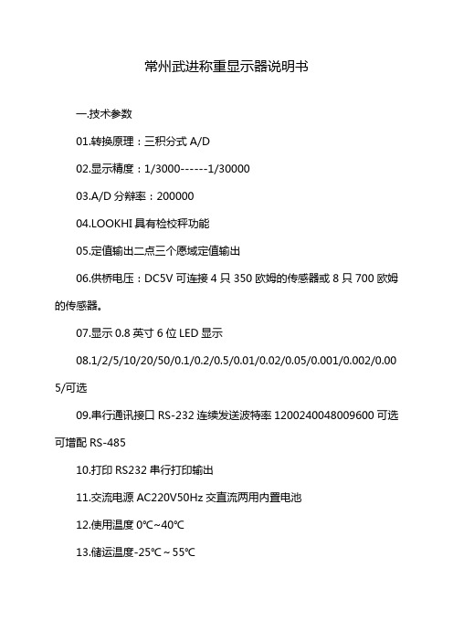
常州武进称重显示器说明书一.技术参数01.转换原理:三积分式A/D02.显示精度:1/3000------1/3000003.A/D分辩率:20000004.LOOKHI具有检校秤功能05.定值输出二点三个愿域定值输出06.供桥电压:DC5V可连接4只350欧姆的传感器或8只700欧姆的传感器。
07.显示0.8英寸6位LED显示08.1/2/5/10/20/50/0.1/0.2/0.5/0.01/0.02/0.05/0.001/0.002/0.00 5/可选09.串行通讯接口RS-232连续发送波特率1200240048009600可选可增配RS-48510.打印RS232串行打印输出11.交流电源AC220V50Hz交直流两用内置电池12.使用温度0℃~40℃13.储运温度-25℃~55℃14.相对湿度≤85%RH15.外型尺寸220mm?40mm?30mm16.重量约2公斤二.安装连接1.传感器连接采用D-九芯孔插座。
2.RS-232C通讯连接:D-9芯针3脚:TXD,5脚:GND3.通讯数据格式(RS-232C连续输出)3.1通信地址Adr=00;连续发送方式,格式为=,X1,X2,X3,X4,X5,X6,发送的X1,X2,X3,X4,X5,X6为显示数据,=为分隔符。
重量:100.00kg,发送:=00.001=00.001=。
3.2.可增配RS-4854.定值输出:D-9芯针6、7脚:低位输出8、9脚:高位输出当称量在低位阀值段时,6、7脚输出闭合开关量信号;当称量在高位阀值段时,8、9脚输出闭合开关量信号。
输出触点容量:0.3A125VAC或0.3A110VDC。
三.按键功能和指示灯说明【STOP】键:停止死机(鸣叫不显示,显示乱码等)【①】键:开/关键【..】键:手动累加功能键【*】键:功能选择键、确认键【一】键:数字移位功能键【t】键:数字增置键,显示?0倍功能键【-0-】键:置零,去除皮重功能键【AC】:交流电工作时亮【→T-】:去除皮重时亮【】:电池电量<30%时亮【AUTO】:自动累计状态时亮【一0-】:处于零位状态时亮【一】:称量稳定时亮【LO】:显示值低于B点阀值【H1]:显示值大于C点阀值【OK】:显示值大于B点阀值,低于C点阀值S四.正常操作1.仪表开机和关机按【①】键,仪表开机。
- 1、下载文档前请自行甄别文档内容的完整性,平台不提供额外的编辑、内容补充、找答案等附加服务。
- 2、"仅部分预览"的文档,不可在线预览部分如存在完整性等问题,可反馈申请退款(可完整预览的文档不适用该条件!)。
- 3、如文档侵犯您的权益,请联系客服反馈,我们会尽快为您处理(人工客服工作时间:9:00-18:30)。
FOR BOARD-TO-CABLE CONNECTION
240R SERIES
s FEATURES
• 1.27 mm (0.050 in.) pitch contact arrangement enables high-density mounting.
•Bellows contacts ensure stable contact preventing pins from bending. The bellows contacts also have excellent stability with repeated insertion and extraction.
•Cables and connectors are assembled by discrete wire IDC.
•Connectors on the cable side provide superb EMI shielding/ESD protection with an inner-metal and outer-plastic dual cover.
•Conforms to IEEE 1284.C Interface
•Tails are spaced in a four-row staggered arrangement (2.54 mm × 1.905 mm) (0.100 in. × 0.075 in.) for easy PC board design.
s SPECIFICATIONS
Specifications
–55°C to +85°C DC 1 A AC 240 V
50 m Ω max. (DC 20 mV, 10 mA)1,000 M Ω min. (DC 500 V)AC 750 V for 1 minute
AWG #28 and #30 stranded wires with φ0.5 to 0.65 mm (0.020 to 0.026 in.) insulation diameter
Item
Operating temperature range Current rating Voltage rating Contact resistance Insulation resistance Dielectric withstand voltage Applicable wire
Materials
Polyester (UL94V-0)Copper alloy Contact Terminal
s MATERIALS
Item
Insulator Conductor Plating
Gold plating Palladium plating
s ORDERING CODE
FCN-24
5D 050-G /E
E:Metal type (board side) or metal type for discrete wire IDC (cable side)
G:Metal type for wire to wire heat bonded multi cable IDC S:Cover
G:Gold plating A:Cover
B:Wide-hole cover Number of contacts: 20,26, 36, 50, 68, or 80Unit type D:Socket R:Plug C:Cover Tail type 0:Cover 4:Straight 5:Right-angle 7:IDC 240 series
Fujitsu connector
240R Series
STRAIGHT SOCKET s DIMENSIONS
s MOUNTING HOLE LAYOUT (COMPONENT SIDE)
s PATTERN INHIBITED AREAS
s RECOMMENDED PANEL DIMENSIONS
s PART NUMBERS AND DIMENSIONS
Number of contacts
202636506880
Part number FCN-244D020-G/E FCN-244D026-G/E FCN-244D036-G/E FCN-244D050-G/E FCN-244D068-G/E FCN-244D080-G/E
A 11.43 (0.450)15.24 (0.600)21.59 (0.850)30.48 (1.200)41.91 (1.650)49.53 (1.950)
B 13.45 (0.529)17.26 (0.679)23.61 (0.929)32.50 (1.279)43.93 (1.729)51.55 (2.029)
C 16.45 (0.647)20.26 (0.797)26.61 (1.047)35.50 (1.397)46.93 (1.847)54.55 (2.147)
D 27.45 (1.080)31.26 (1.231)37.61 (1.480)46.50 (1.830)57.93 (2.280)65.55 (2.580)
E
33.35 (1.312)37.16 (1.462)43.51 (1.712)52.40 (2.062)63.83 (2.512)71.45 (2.812)
F 23.30 (0.917)27.11 (1.067)33.46 (1.317)42.35 (1.667)53.78 (2.117)61.40 (2.417)
Unit: mm (in.)
240R Series
© 2005 Fujitsu Components America, Inc. All company and product names are trademarks or registered trademarks of their respective owners. Rev. 01/17/2005.
Japan
Fujitsu Component Limited Gotanda-Chuo Building
3-5, Higashigotanda 2-chome, Shinagawa-ku Tokyo 141, Japan Tel: (81-3) 5449-7010Fax: (81-3) 5449-2626
Email: promothq@ Web: North and South America
Fujitsu Components America, Inc.250 E. Caribbean Drive
Sunnyvale, CA 94089 U.S.A.Tel: (1-408) 745-4900Fax: (1-408) 745-4970
Email: marcom@ Web:
Europe
Fujitsu Components Europe B.V.Diamantlaan 25
2132 WV Hoofddorp Netherlands
Tel: (31-23) 5560910Fax: (31-23) 5560950
Email: info@ Web: Asia Pacific
Fujitsu Components Asia Ltd.102E Pasir Panjang Road
#04-01 Citilink Warehouse Complex Singapore 118529Tel: (65) 6375-8560Fax: (65) 6273-3021
Email: fcal@
Fujitsu Components International Headquarter Offices。