VP2140 40V3A降压稳压器
PR6214
5/6
OC
Cable comp.
INV
3
S/H + 3.0V -
CC/CV
LEB
4
CS
2
COMP
GND
7
绝对最大值
符号 VDD VINV VCS VCOMP IC RθJA TL TSTG TJ VDD 电压 INV输入电压 CS输入电压 COMP输入电压 内置BJT集电极电流 封装热阻 SOP7(环境温度85℃) 引脚压焊温度 存储温度范围 工作结温范围 SOP7 (10S) 参数 范围 0~25 -0.3 to 5V -0.3 to 5V -0.3 to 5V 0.8 150 260 -55 to + 150 -20 to + 150 单位 V V V V A ℃/W ℃ ℃ ℃
3/7
PR6214
高精度恒流/恒压(CC/CV)原边反馈功率转换器
电气参数
(Ta=25°C ,除非特殊说明, VDD = 15.0V)
符号 供电电源 (VDD)
IDD_ST IDD_OP
UVLO(ON) UVLO(OFF)
参数
测试条件
最小值
典型值
最大值
单位
启动电流 静态工作电流 进入欠压锁定阈值电压 退出欠压锁定阈值电压 过压保护阈值电压
(6)
V1.0
6/7
PR6214
高精度恒流/恒压(CC/CV)原边控制功率开关
封装尺寸
SOP-7L
Symbol A A1 A2 A3 b b1 c c1 D E E1 e e1 L L1 L2 R R1 h θ1 θ2 θ3 θ4
Min. 1.35 0.10 1.25 0.50 0.39 0.28 0.10 0.10 4.8 5.8 3.8
沈阳新维AMDP-D731 系列电动机保护器使用说明书

AMDP-□/D731 系列电动机保护器使用说明 产品概述主要特点:DSP 为核心,数字设定,数字显示,保护功能完备、保护性能可靠,2路与采集、保护 电路及DSP隔离、参数可设置电流范围的4-20mA输出。
检测、显示电压,除保护电动机的继电器触点输出信号外,还配有6个故障类型、1个故障预警、1个故障报警输出信号和1个清除故障状态输入信号。
保护功能:缺相、短路、接地、堵转、过载、电流不平衡、过压、欠压。
适用范围:额定电压不高于1140V,频率为50Hz或60Hz的三相交流电动机。
电动机保护器型号 AMDP-0.5 AMDP-1 AMDP-2AMDP-5AMDP-10AMDP-20AMDP-50 AMDP-100 AMDP-150AMDP-200最大设定电流(A) 0.55 1.1 2.3 5.5 11 23 55 110 165 220 最小设定电流(A) 0.1 0.2 0.4 1 2 4 10 20 30 40 电动机最大功率(KW) 0.22 0.4 1.1 2.2 4 11 22 45 75 110 电动机最小功率(KW) 0.055 0.11 0.22 0.55 1.1 2.2 5.5 11 18.5 22 电动机电源穿线孔Φ(mm)20 20 20 20 20 20 20 20 30 30 连接电缆:连接主单元与电流检测单元,6×0.3mm²×2.2 m双绞屏蔽电缆工作电压:AC 85V — 265V、DC 85V — 265V功率消耗:小于 2W检测电压:AC 0 — 500V(电压显示值可由参数设为检测值的1、1.732、3、5.196倍)采集精度:0.5环境温度:- 20℃ — 50℃继电器触点:1常开触点,AC 250V/10A(阻性负载)、DC 30V/10ADO/DI电压: DC 24V±10% Array DO驱动能力:最大100mA(DO1-DO8每路最大100mA)4-20mA负载电阻:小于600ΩAMDP-□/D731系列电动机保护器工作过程AMDP-□/D731 系列电动机保护器在电动机未发生故障时,显示电动机A、B、C相电流、电压,电动机故障类型输出信号DO1-DO6、故障预警输出信号DO7、故障报警输出信号DO8输出高电平;当电动机发生接地、短路、缺相、堵转/过载/电流不平衡、过压、欠压故障时,对应的故障类型输出信号(DO1-DO6中的1个)及故障预警输出信号DO7输出低电平,当故障持续到设定的报警时间,继电器触点O11、O12断开停止电动机运行(故障灯亮),故障预警输出信号DO7输出高电平,故障报警输出信号DO8输出低电平,保护器显示故障代码指示故障类型,并且显示电动机发生故障时的A、B、C相电流、电压。
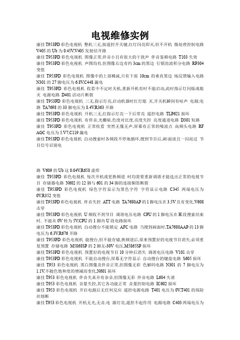
中文TPS54340DDAR 42V 输入,3.5A,降压直流-直流转换器,具有Eco-mode

0102030405060708010000.51.01.52.0I - Output Current -AO E f f i c i e n c y - %2.53.090 3.5Product FolderSample &BuyTechnical Documents Tools &SoftwareSupport &CommunityTPS54340ZHCSAC5B –OCTOBER 2012–REVISED MARCH 2014TPS5434042V 输入,3.5A ,降压直流-直流转换器,具有Eco-mode™1特性3说明•输入电压范围4.5V 至42V (最大绝对值45V )TPS54340是一款42V ,3.5A ,降压稳压器,此稳压器具有一个集成的高侧MOSFET 。
按照ISO 7637标• 3.5A 持续电流,4.5A 最小峰值电感器电流限值准,此器件能够耐受高达45V 的抛负载脉冲。
电流模•电流模式控制直流-直流转换器式控制提供了简单的外部补偿和灵活的组件选择。
一•92m Ω高侧金属氧化物半导体场效应晶体管(MOSFET)个低纹波脉冲跳跃模式将无负载时的电源电流减小至•轻负载条件下使用脉冲跳跃实现的高效率Eco-146μA 。
当启用引脚被拉至低电平时,关断电源电流mode™被减少至1μA 。
•轻负载条件下使用集成型引导(BOOT)再充电场效欠压闭锁在内部设定为4.3V ,但可用使能引脚将之提应晶体管(FET)实现的低压降高。
输出电压启动斜升由内部控制以提供一个受控的•146μA 工作静态电流启动并且消除过冲。
•1μA 关断电流•100kHz 至2.5MHz 的固定开关频率宽开关频率范围可实现对效率或者外部组件尺寸的优•同步至外部时钟化。
频率折返和热关断在过载条件下保护内部和外部•可调欠压闭锁(UVLO)电压和滞后组件。
•内部软启动TPS54340采用8端子散热增强型HSOIC •精确逐周期电流限制PowerPAD™封装。
78L05耐压40V稳压器规格书

78L05单片集成电路稳压器的一种型号。
此类元件应用十分广泛,全系列的稳压器中都有滤波电路,从而有效地降低了噪声和外界的干扰,每种稳压器均能达到100mA 的电流输出,内部设有过流、过热自动保护功能。
特点1. 三端稳压器2. 最大输出电流100mA3. 独立工作无须外加部件4. 内部有热过载保护装置5. 内部有电流短路保护功能三、应用1. 直流电源2. 充电器3. 适配器4. DVD5. 电视机6. 录音机PW6206,PW6513系列是一款高精度,高输入电压,低静态电流,高速,低压降线性稳压器具有高纹波抑制。
在VOUT=5V&VIN=7V时,输入电压高达40V,负载电流高达300mA,采用BCD工艺制造。
PW6206提供过电流限制、软启动和过热保护,以确保设备在良好的条件下工作PW6206是SOT23-3L封装,PW6513是SOT89-3封装。
特点输入电压:4.75V~40V输出电压:1.8V~5.7V输出精度:<±2%输出电流:150mA(典型值)最高300mA@VIN=7V,VOUT=5V,PW6206B50HV封装电源抑制比:60dB@100Hz跌落电压:600mV@IOUT=100mA静态电流:4.2μA@VIN=12V(典型值)ESD HBM:8KV推荐电容器:10uFHigh Input Voltage LDO Linear RegulatorsGENERAL DESCRIPTIONThe PW6513 series is a high accuracy, high input voltage low quiescent current, high speed, and low dropout liner regulator with high ripple rejection. The input voltage is up to 40V and load current is up to 300mA at VOUT = 5V & VIN = 7V. The device is manufactured with BCD process. The PW6513 offers over-current limit, soft start and over temperature protection to ensure the device working in well conditionsThe PW6513 regulators is available in standard SOT89-3L packages. Standard products are Pb-free and Halogen-free.FEATURES⚫Input voltage: 4.75V~40V⚫Output voltage: 1.8V~5.7V⚫Output accuracy: < ±2%⚫Output current: 150mA (Typ.)⚫Up to 300mA @ VIN = 7V, VOUT = 5V,⚫PSRR: 60dB @ 100Hz⚫Dropout voltage: 600mV @ IOUT = 100mA⚫Quiescent current: 4.2μA @ VIN = 12V(Typ.)⚫ESD HBM: 8KV⚫Recommend capacitor: 10μFAPPLICATIONS⚫Smart electric meter⚫In-car entertainment⚫Electric bicycleTYPICAL APPLICATION CIRCUITPIN ASSIGNMENT/DESCRIPTIONRECOMMANDED OPERATING RANGEPW6513A PW6513BAbsolute Maximum Ratings (note)Note: Exceed these limits to damage to the device. Exposure to absolute maximum rating conditions may affect device reliability.SIMPLIFIED BLOCK DIAGRAMVINVOUTELECTRICAL CHARACTERISTICSTYPICAL PERFORMANCE CHARACTERISTICS0510152025110100100010000100000I Q (u A )IOUT (uA)IQ vs. IOUTVin=5V Vin=10V Vin=20V Vin=30VAPPLICATION INFORMATIONINPUT CAPACITORAn input capacitor of 10μF is required between the VIN and GND pin. The capacitor shall be placed as close as possible to VIN pin, and the use of electrolytic capacitors is recommended. The tolerance and temperature coefficient must be considered in order to ensure the capacitor work within the operation range over the full range of temperature and operating conditions.OUTPUT CAPACITORIn applications, it is important to select the output capacitor for stable operation. The minimum capacitance for stable and correct operation is 1μF. The capacitance tolerance sho uld be ±30% or better over the operation temperature range. The recommended capacitor type is MLCC.NO-LOAD STABILITYThe PW6513 will remain stable and in regulation with no external load. This is especially important in CMOS RAM keep-alive applications.TYPICAL CIRCUITThe following figure shows a typical application circuit for the PW6513 devices. The value of external components shall be chosen carefully, depending on the application. In plugging application, because the overshoot caused by the insertion and withdrawal of power on the chip may damage the chip, it is recommended that VIN be less than 30V and the input voltage spike should not exceed 45V.In plugging application, it is suggested that R, C1 are selected as following:1.C1=10μF ~ 100μF electrolytic capacitor with maximum voltage greater than 50V, R=0;2.C1=1μF ~ 10μF MLCC with maximum voltage V greater than 50V and R=2Ω in the type of 1206- the resistor shall be carefully chosen to make sure enough margin to sustain the surge current during plugging.PW6513_2.2PACKAGE DESCRIPTIONSOT89-3L。
康佳电视故障解决方法大全
电视维修实例康佳T953PD彩色电视机整机三无,按遥控开关键,红灯闪亮即灭,但不开机微处理控制电路V405的Ub为0.45V,V405发射结开路康佳T953PD彩色电视机图像正常,伴音小且有很大的干扰声伴音鉴频电路T103失效康佳T953PD彩色电视机声图均有,但图像右边有约3cm的黑边行锯齿波积分电路RP304变值康佳T953PD彩色电视机图像中的上部稀疏,只有下部10cm的垂直黑边场反馈输入电路N301的27脚电压为6.8V,C448漏电康佳T953PD彩色电视机收看中不定时关机,重新开机有时不能启动,此时指示灯闪烁或熄灭电源电路D401活动片断裂康佳T953PD彩色电视机三无,指示灯亮,启动机器时红灯熄灭,开关机瞬间有咕声电源;电路TA7698的33脚电压为8.4V,R363开路康佳T953PD彩色电视机开机三无,红指示灯亮一下后常亮遥控电路TLP621损坏康佳T953PD彩色电视机有伴音,光栅暗,色度对比度,亮度失控亮度通道电路D301短路康佳T953PD彩色电视机正常收看突然无像无声,屏幕有正常的噪波点高频头电路RF AGC电压为5.V7,C119漏电康佳T953PD彩色电视机自动搜索时各频段不停地循环,搜到节目后,画\面淡且一闪而过节目信号识别电路V609的Ub这0.04V,R658虚焊康佳T953PD彩色电视机每次开机或更换频道时均需要重新调谐才能选出正常的电视节目存储器电路N602的12脚与601的34脚的连接铜箔断裂康佳T953PD彩色电视机绿色字符显示为黑色字符字符显示电路C345两端电压为0V,R352变值康佳T953PD彩色电视机伴音失控ATT电路TA7680AP的1脚电压在3.5V且有变化,V608击穿康佳T953PD彩色电视机U频收不到节目调谐电压电路CPU的1脚电压在H段搜索结束时, 不能从0V转为5V,CPU的1脚内U段电路损坏康佳T953PD彩色电视机自动搜台不能锁定AFC电路当搜到画面时,TA7680AAP的13脚电压为6.3V,R676开路康佳T953PD彩色电视机能搜台,但不能存储,换频道后,原来预置好的电视节目消失,必须重复预置存储电路M5868SP的2脚无-30V电压,M5865SP损坏康佳T953PD彩色电视机预置好的电视节目10分钟后消失调谐电压电路V101击穿康佳T953PD彩色电视机不能自动搜台,屏幕无字符显示自动搜台的键盘电路S605损坏康佳T953彩色电视机黑白图像及伴音正常,但图像无彩色解码电路N301的7脚电压为1.1V,不随色饱和度的增减而变化,N601损坏康佳T953彩色电视机伴音失真并有杂音,但图像无彩伴音电路L604失谐康佳T953彩色电视机音量失控,其它各功能正常音量控制电路IC602损坏康佳T953彩色电视机开启电源后无任何反应遥控电源电路T401电压为0V,T401的保险丝熔断康佳T953彩色电视机开机无光,无音,电源灯亮,遥控不起作用电源电路C403两端电压为20V,电源开关组件下面的红色纸片漏电康佳T953彩色电视机收看中突然无声无像,屏幕有正常的噪波RFAGC电路RFAGC电压为5.7V,C119漏电康佳T953彩色电视机U段接收正常,V段无图无声VHF电压控制Q606 Uc正常为11.5V,R628开路康佳T953彩色电视机无光无声,无字符显示,指示灯随开关而亮灭行扫描电路行回扫变压器因高压击穿,并烧坏偏转线圈康佳T953彩色电视机图像上有虚线斜条,且斜条飘忽不定场输出电路C453漏电康佳T953彩色电视机图象模糊,伴音失真中放电路N101的11脚电压为5.25V,C119漏电康佳T953彩色电视机开机正常,一会变为白光成A V状态图像通道电路N101的15脚电压为4V,5脚电压为6.8V,C116失效康佳T953彩色电视机绿色字符显示为黑色字符,节目不能存储,转换频道后,原电视节目消失,必须重复预置存储器电路N602的12脚无电压,R352开路康佳T953彩色电视机伴音换控伴音电路V608击穿康佳T953彩色电视机U段收不到节目微处理电路N601在H段搜索时不能从0V转为5V,N601损坏康佳T953彩色电视机自动搜台锁不住AFT电路N101的13脚电压在 6.36V上下摆动,V604击穿康佳T953彩色电视机电视节目10分钟左右消失高频头调谐电压电路BT端电压为20.3V,V101损坏康佳T953彩色电视机在收看过程中,机内冒烟且有打火声,即三无,发出吱吱声自动亮度电路R425变值康佳T953彩色电视机整机三无,亦无字符显示,按遥控电源键时,红灯亮过压保护电路V305的Uc为0.6V,R426开路康佳T953彩色电视机整机三我,屏幕无显示,待命灯亮时钟脉冲电路N601的28,29脚无脉冲,Z601漏电康佳T953彩色电视机通电后,面板上的红灯亮,但整机三无,亦无字符显示待命电源电路N60117脚电压为4.6V,R669变值,C611漏电康佳T953P彩色电视机开机工作一段时间后,机器突然无光无声,关机后一会又能重新开机,但故障又重复保护电路VD301失效康佳T953P彩色电视机开机工作一段时间后,机器突然无光无声,关机后一会又能重新开机,但故障又重复取样电路RP401不良康佳T953P彩色电视机电源灯亮,按遥控器开机键,电源灯灭,电视机无光无声可控硅保护电路V407开路康佳T953P彩色电视机接通电源开关,电源灯不亮辅助电源电路VD403负端无16V电压,VD401也无-30V电压,遥控变压器开路康佳T953P彩色电视机图像模糊且有回扫线行扫描电路C455漏电康佳T953P彩色电视机屏幕上有色斑消磁电路T401损坏康佳T953P彩色电视机图像模糊,伴音失控AGC电路N101的(11)脚电压为0.5V(正常为5.25V),C119漏电康佳T953P彩色电视机无光栅,无伴音,无字符显示, 按遥控器的开/关机键,面板上红指示灯能亮灭,但不能开机行扫描电路V405的Ub为2V(正常为0.45V),V405击穿康佳T953P彩色电视机黑白图像基本正常,但无彩色,伴音较小且噪声大中频前置放大电路SA101损坏康佳T953P彩色电视机一条水平亮线. 场扫描电路IC401的(3)'(6)脚无电压,R431断路. 康佳T953P彩色电视机开机"三无",且伴有"嘟嘟"声一条水平亮线行扫描电路+B无电压输出.C420漏电.康佳T953P彩色电视机开机2分钟后行失步,关机后再开机,故障重现AFC电路C343(0.47υF/50V)容量失效.康佳T953P彩色电视机绿色字符显示为黑色字符字符显示电路R352失效康佳T953P彩色电视机U频道节目收不到频段切换电路N601的1脚电压在U段不能从0V回转为5V.N601损坏.康佳T953P彩色电视机能自动搜台,但不能锁台AGC脉冲输入电路N101的13脚电压在6.36上下摆动,C610开路失效康佳T953P彩色电视机设置好的电视节目10分钟后消失调谐电压控制电路V101不良康佳T953P彩色电视机能自动搜台,但屏幕无字符显示键盘电路S605断路康佳T953P彩色电视机音正常,图像模糊,约半小时后清晰显像管及管座显像管11脚与12脚的反向电阻为0Ω,显像管管座KB漏电康佳T953P彩色电视机伴音正常,暗无像亮度通道电路N301的8脚电压8.4V,D301短路康佳T953P彩色电视机每次开机或更换频道时均需重新调谐才能收看存储器控制电路N602的12脚与34脚断裂康佳T953P彩色电视机搜台时各频段不停地循环搜索,画面淡且一闪而过同步信号校正电路V609的Ue为0.04V,R658开路康佳T953P彩色电视机选台时只能选到部分电台,且图象不稳,无法收看调谐电压电路BP 端只能在0-24V间变化,C102漏电康佳T963A彩色电视机自动搜台时,图像在屏幕上只稳定1秒就继续搜台,节目不能锁定存储器电路IC602损坏康佳T963A彩色电视机开机一切正常,10分钟后光栅压缩行扫描电路Q402击穿康佳T963A彩色电视机伴音正常,图像清晰度模糊图像中放电路iC101的11脚电压为4.4V,C117漏电康佳T963A彩色电视机图像及伴音正常,只是关机后出现色斑消磁电路TH901开路康佳T963A彩色电视机无光,无声,无像电源电路T901损坏康佳T963A彩色电视机无光无声,无像行扫描电路IC301振荡电路坏康佳T963A彩色电视机无光,无声,无像微处理控制电路X601失效康佳T963A彩色电视机无光无音,无像开关电源电路CD901击穿康佳T963A彩色电视机图像伴音正常,光栅亮度比正常亮,同时机内有叭啦,叭啦的火花声电源电路Q901熔断康佳T963A彩色电视机出现大面积爬行且色调畸变色解码电路IC301的17,19脚电压为4V,C350漏电康佳T963A彩色电视机黑白图像正常,但无彩色;亦无伴音,自动搜索不停,且有时仍自动关机行逆程脉冲传输出电路IC301的(36)脚电压1.7V(正常为2.9V;(38)脚电压为0.3V(正常为0.6V),C303开路康佳T963A彩色电视机开机后无光栅,无伴音,待机指示灯和环绕声指示灯亮,手控,遥控全部失灵微处理控制电路C600漏电康佳T963A彩色电视机开机后无光栅,无伴音,待机指示灯和环绕声指示灯亮,手控,遥控全部失灵微处理控制电路C600漏电康佳T963A彩色电视机伴音小鉴频电路T103失谐康佳T963A彩色电视机无图无声,有浓密的噪波点中放通道电路V117漏电康佳T963A彩色电视机场线性差场扫描电路C452漏电康佳T963A彩色电视机灵敏度低中放通道电路C117漏电康佳T963A彩色电视机VHF频段节目正常,UHF频段节目收看约2小时后跑台高频头高频头损坏康佳T963A彩色电视机黑白图像着色慢且有重影色解码电路, C301的18脚电压为8.1V,R349开路康佳T963A彩色电视机字符随光栅颜色而变字符显示电路D616虚焊康佳T963A彩色电视机图像正常,无伴音伴音电路TDA2009A的6脚电压不稳,C339松动康佳T963A彩色电视机各频段搜索不停,电视画面开始时稳定,随之行失步,2秒后继续搜索AFC电路T104失调康佳T963A彩色电视机正常收看10分钟后,电视机信号丢失,满屏噪点高频头调谐供电电路R601变值康佳T963A彩色电视机自动或半自动搜台时有彩色,结束彩色丢失,黑白图像正常微处理控制电路CF8581损坏康佳T963A彩色电视机开机20分钟后光栅亮度下降,图像变淡遥控接口电路TA7698AP 稳定性差康佳T963A彩色电视机开机,整机处于预备状态,约1小时后自动开机,声图正常微处理控制电路PCA84C640的41脚电压为0V,PCA84C640损坏康佳T963A彩色电视机伴音正常,但屏幕为暗红色光栅,无图,有回扫线,字符亮度下降字符信号通路Q505的Ue由134.5V降至88V,Q610击穿康佳T963A彩色电视机声图正常,字符边界拉丝,字符颜色随画面变化而变化PCA84C640的消陷驱动电路字符显示消隐脉冲电路,C633失效康佳T963A彩色电视机声图正常,遥控时有字符显示,但字符偏左PCA84C640的RC时钟振荡电路PCA84C640的时钟振荡频率高于100MH,VR601变值康佳T963A彩色电视机彩色时深时淡且有干扰色同步脉冲检波负载滤波电路IC301的7脚电压为5.3V,C339虚焊康佳T963A彩色电视机图像正常,但无音伴音功放电路IC201的2,4脚电压为0.7V,Q204断路康佳T963A彩色电视机正常收看10分钟后,节目丢失,随即满屏噪点PCA84C640的14位D/A转换电路ZD001两端电压30V,R601增值康佳T963A彩色电视机开机20分钟后,光栅亮度下降,图像变暗亮度通道电路IC301的42脚电压为6.4V,IC301内热稳定性差康佳T963A彩色电视机光栅为一条水平亮线场扫描电路IC402损坏康佳T963A彩色电视机有音,无像行扫描电路R411变值康佳T963A彩色电视机无光无音开关电源R911开路康佳KK-T2103彩色电视机有光,无像中放通道 C120漏电康佳KK-T2103彩色电视机有像无声伴音电路IC201损坏康佳KK-T2103彩色电视机无光,无声行扫描电路Q402击穿康佳KK-T2103彩色电视机无光无声电源电路D904击穿康佳KK-T2103彩色电视机屏幕上呈现白光栅,无像,伴音正常视频放大电路TA8759BN的35脚电压正常为1.35V,D305开路康佳T2106彩色电视机屏幕暗,呈现模糊的彩色图像,但伴音和字符显示正常亮度通电路C370开路康佳T2106彩色电视机屏幕呈一条水平亮线场扫描电路TA8759BN的31脚电压为0.2V,29脚电压为0V,ZD301击穿康佳T2106彩色电视机无光栅,无图像,无伴音行扫描电路Q401的Uc为70V,C402漏电康佳T2106彩色电视机无光栅,无图像,无伴音开关电源电路+140V升至为+200V,F901熔汤康佳T2106彩色电视机图像正常,无伴,调节音量键,屏幕上的音量标志正常变化伴音中放电路IC0018-10脚电压为5.98V,C012严重漏电康佳T2106彩色电视机自动搜台锁不住节目AFT电路IC001的20脚电压为4.8V,C606漏电康佳T2106彩色电视机图像正常,遥控或手控调节音量时,屏幕能显示音量逐渐增大或减小,但仅有微弱的伴音且不随音量的调节变化电子音量衰减电路IC1101的20脚电压为4.8V,V626漏电康佳T2106彩色电视机自动和手动均不能锁台微处理控制电路IC601的51脚电压为1.91V,V608漏电康佳T2106彩色电视机图像正常,无音伴音中放电路IC001的9脚电压为0.8V,C102漏电康佳T2114彩色电视机伴音失真伴音电路Z210失效康佳T2114彩色电视机光栅呈一条水平亮线场扫描电路L405开路康佳T2114彩色电视机整机三无,无待机指示,开机有吱吱声开关电源电路V008的Ub为0V,C059击穿康佳T2506彩色电视机AGC失效,各种制式下图像和伴音均是信噪比差,调VR001无效中放电路调VR001时,同时测IC001的7脚电压无变化,IC001损坏康佳T2506彩色电视机PAL制,NTSC制和SCEAM制均无图像,无伴音中放电路IC001的1,2脚电压为5.4V,IC001损坏康佳T2506彩色电视机左声道声音小有杂音伴音功放电路IC801(TDA2009)性能不良康佳T2506彩色电视机图像上部拉长,下部严重压缩场扫描电路C426(330μF/25V)漏电康佳T2506彩色电视机无光栅,无伴音,无图像开关电源电路F901熔断;C911失效康佳T2510彩色电视机自动搜台时锁不住AFT电压电路TA8611第20脚电压为4.8V,C606漏电康佳T2510彩色电视机人正常的图像,无伴音,但调节音量键时,屏幕上的音量标志变化正常伴音功放电路YA8611第8,9脚电压为1.6V,C012漏电康佳T2510彩色电视机正常收看一段时间后,图像逐渐扭曲,伴音逐渐失真,最后节目消失,重新调台,故障重复出现电子调谐器及供电电路MN1528KWE第39脚电压为3.2V,Q619为21V,电子调谐器不良康佳T2510彩色电视机刚开机正常,工作4分钟后PAL制色色彩消失,调节色度钮无效,停机30分钟后开机又重复本故障色同步选通门电路TA8759第34脚电压为3V,C319漏电康佳T2510彩色电视机在接收中,H段突然声图皆无,但L,U频段一直正常H频段控制电路高频头第6脚电压为12V,V104虚焊康佳T2510彩色电视机开机屏幕呈很亮的光栅,数秒后光栅消失,但伴音正常亮度电路R416开路康佳T2510彩色电视机开机后无光栅,但伴音完好过压保护电路IC801第30脚电压为0V,C513漏电康佳T2510彩色电视机开机后无光栅,但伴音完好X射线保护电路TA7698AP第30脚电压为0V,C622开路康佳T2510彩色电视机无光栅,无伴音开关电源电路STR-6309击穿康佳T2512A彩色电视机AGC失控,各种制式下图像和伴音均是信噪比差,调VR001无效中频通道电路TA8411的7脚电压无变化,T8611损坏康佳T2512A彩色电视机PAL制,NTSC制SCEM制均无像,无音中频通道电路TA8611的1,2脚电压为2.6左右,TA8611损坏康佳T2512A彩色电视机图像正常,无音,只有沙沙声,噪声大小可调伴音中频通道电路T8615第12脚无波形,C104断路康佳T2512A彩色电视机字符显示正常,但手动和自动寻台时各频段无图像, 中放电路高频头第5脚电压为3.9VC003开路康佳T2512A彩色电视机伴音正常,但图像彩色时有时无PAL解码电路TA8759N 25脚电压为5.6V,C332开路康佳T2512A彩色电视机重放SECAM制节目时,屏幕全红,而其它制式节目正常SECAM色解码电路TA8759第64脚电压为7V,C346击穿康佳T2512A彩色电视机每次开机收看约10分钟,光栅变暗,遥控和手控不能调大亮度亮度信号处理电路TA8759第51脚电压为5V,C349漏电康佳T2512A彩色电视机自动搜台正常,手动搜台时无PAK屏显,无像无音搜台编码与解码电路MN15287WE第13脚电压始终为0V康佳T2512A彩色电视机图像为黑而模糊的彩色影像,调小色饱和度只有暗淡的光栅亮度电路TA8759第59脚电压为0V,TA8759损坏康佳T2512A彩色电视机光栅时有时无,行不同步同步分离电路TA8759第29脚电压为0.73V,C310短路康佳T2512A彩色电视机接收NTSC制节目时,图像的水平位置偏左行中心校正电路Q308损坏康佳T2512A彩色电视机在任何制式光栅均不满屏场锯齿波形成电路TA8759N第31脚电压为6.6V,C323不良康佳T2512A彩色电视机无伴音,只有较大的嗡嗡声中放电路C294严重漏电康佳T2512A彩色电视机三无,红灯亮电源稳压电路V901的Ub 为-2.6V,VD917击穿康佳T2512A彩色电视机开机红灯不亮,按键不起作用,有光有噪声+5V稳压电源电路N601的52脚无电压,V908击穿康佳T2512A彩色电视机开机红灯不亮,按键不起作用,有光,有雪花,有噪声,无图+5V稳压电源电路N601的52脚电压为4.95V,27脚电压为4.91V,R918开路康佳T2916A彩色电视机三无,电源灯不亮偏置电路+B电压为0V,V908击穿康佳T2916A彩色电视机三无,民源灯亮开关电源电路+B电压降到0.7V,V901的Ue为0V,R951一脚虚焊康佳T2916A彩色电视机三无,电源灯亮输出电路+B电压上升到38V即下降至0V,V402击穿康佳彩电维修1.康佳T914H三无拆机发现F402断,C443、C436爆裂,说明三无故障是由于电源电压输出过高引起的。
多功能、多种拓朴高频PWM控制器TPS43000

多功能、多种拓朴高频PWM控制器TPS43000TPS43000是一款高频电压型同步PWM控制器,它能用于BUCK、BOOST、SEPIC 或flyback拓朴的控制。
该款高度柔性,全新特色的控制器设计成可驱动一对外部功率MOSFET(一个为N沟,一个为P沟)的结构,因而具有很宽范围的输出电压和功率水平,还有自动的PFM模式工作,关断电流小于1μA,休息模式工作电流小于100μA,在1MHz时整个工作电流小于2mA,因而是一个高效率多用途的DC/DC控制器。
TPS43000输入电压范围从1.8V~9.0V,给分布式系统供电,可以由镍镉电池供电,也可以由锂电池供电,产生0.8V~8V的各输出电压(还可更高),用户可调节其PWM频率最高达2MHz,也可令其进入PFM模式,在此时若电感电流进入断续,则IC进入休息模式,在输出电压降下2%时再工作,在此工作模式,在很宽的负载电流时都有非常高的效率,器件还可以同步到外时钟频率。
TPS43000可选择两个水平的限流电路,它检测主功率MOSFET的压降,用户可选择逐个脉冲式限流,或打呃式过流保护。
TPS43000可以在低功耗模式下工作,有欠压锁定,软起动等功能,最高工作频率达2MHz。
IC的内部等效电路如图1所示。
其16PIN功能描述如下:1 PIN SYNC/SC此功能端用于外同步及关断控制,要求外脉冲从0V~2V,占空比不限,但脉宽必须大于100ns。
保持此端高于2V,或保持此电压达35μS,IC 即关断。
2 PIN CCS限流端子,可逐个脉冲电流限制及打呃式限制,将此端接于VIN,为逐个脉冲限流,接此端到GND,进入打呃式过流保护。
3 PIN RT外接电阻到GND设置工作频率。
4 PIN CCM无论输入端检测有没有信号,I ZERO比较器都允许断续型工作,将此端电平拉高,可忽视I ZERO比较器的输出,强制连续导通模式工作,将其接地,即使能I ZERO,允许断续导通模式工作。
AFT故障的故障及检修方法

AFT故障的故障及检修方法《家电维修》1、海信TC2125 (A3)机心自动搜索时能把所有的节目识别出来,并存储,图像清晰,恢复正常收看后,个节目都偏离正常位置:AFT电路V121漏电。
2、海信TC2140M(CPU M37211M2-562SP)(小信号处理TDA8361)搜索识别和位置正常,搜索完后一个节目也没有,原先存的节目基本正常,换CPU,存储器不能解决故障,固定高频头AFT电压,出现清晰图像和伴音:AFT电路有一个三极管击穿。
判断AFT电路故障方法:进入手动微调状态,向上或向下,声图有较大变化或手动微调能声像俱佳,退出后变差,就认定AFT电路故障。
2002.3.3索尼背投彩电检修实例(上) 2002.3.41、指示灯亮,无光栅,无伴音:IC803(CA0007AD)坏,投影管漏油。
2、屏幕中心由一个一分硬币大小的圆形污斑:有一个投影管不良。
3、红光栅,回扫线:聚焦组件某一引线虚焊。
4、有时屏幕上无字幕,有时还伴有水平聚焦变差现象,垂直聚焦良好:IC501(2)D527(5V)击穿。
索尼大屏幕彩电慢性绿色故障的检修 KV-L34MF1 从左到右慢慢变绿:消磁控制电路故障,应急改进方法。
2.5用飞利浦CTV-222S遥控系统改造索尼KV-2553TC彩电。
02.3.6长虹C2588(NC-2)彩电屡烧行管:光电耦合器NQ826集电极R842(56欧)变大为140K。
02.3.7海尔HT 2529彩电换太黑屏的取消方法 02.3.8图像内容影响场副总线控制扑朔迷离东杰EK2198A (小信号处理TV1231N),(CPU TMP87CK38N)图像向中间压缩,忽大忽小:进入维修状态,调MOD0,MOD1. 02.3.8高路华TC2528 CPU(34300N4-721SP)每次开机进入AV状态(待机状态)的解密方法。
02.3.8TDA4501.TDA8305(27)C416介质损耗变变大(行逆程电容变质引起沙堡异常)引起故障现象是行幅略有缩小,右侧有一垂直黑带。
tps54540
Copyright © 2013, Texas Instruments Incorporated English Data Sheet: SLVSBX7
TPS54540
ZHCSB47 – MAY 2013
This integrated circuit can be damaged by ESD. Texas Instruments recommends that all integrated circuits be handled with appropriate precautions. Failure to observe proper handling and installation procedures can cause damage.
2
PRODUCTION DATA information is current as of publication date. Products conform to specifications per the terms of the Texas Instruments standard warranty. Production processing does not necessarily include testing of all parameters.
HSOIC PACKAGE (TOP VIEW)
BOOT
1
8
SW
VIN
2
Thermal 7
Pad
EN
3
9 6
GND COMP
RT/CLK
4
5
FB
PIN FUNCTIONS
PIN
I/O
NAME
NO.
DESCRIPTION
微昂 ME6214 低功耗低压差大电流线性稳压器说明书
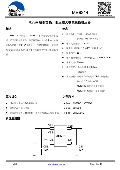
ME62140.7uA 超低功耗、低压差大电流线性稳压器概述ME6214系列是以 CMOS 工艺制造的超低静态功耗、低压差线性稳压器。
稳压器消耗电流约0.7uA ,使能关断后功耗为0.01uA (典型)。
内置使能控制,限流电路以及折返短路保护,并有使能控制输出电容自动放电功能。
特点 ● 超低功耗:工作时:0.7uA (典型) 休眠时:0.01uA (典型) ● 输入电压范围:2.0~18V● 输出电压范围:1.5~5.0V (间隔0.1V ) ● 输出精度:±2%● 输入输出电压差:160mV@ I OUT =100mA (3.3V ) ● 输出电流:300mA● 电流保护: 折返短路电流30mA过流保护● 使能控制:高电平ON/低电平OFF ,不能悬空 输出电容自动放电功能 ME6214C 系列为带使能版本 ME6214A 系列为不带使能版本 应用场合 封装形式● 以电池供电的设备的稳压电源 ● 3-pin SOT89-3,SOT23-3 ● 家电产品的稳压电源 ● 5-pin SOT23-5 ● 携带通信设备、数码相机、数码音响设备的稳压电源 ● 6-pin DFN2X2-6L典型应用图VoutNCCE VSSVIN CIN1uFCIN 1uFME6214选购指南1. 产品型号说明ME 62 14X XX XG环保标识封装形式M3-SOT23-3 M5-SOT23-5版本或功能产品品种产品类别公司标识输出电压如:A-无使能 C-有使能P-SOT89-3 N6-DFN2*2-6L目前产品的电压值共有5种:1.5V 、1.8V 、2.8V 、3.0V 、3.3V 、4.5V 、5.0V 。
如需其他电压值或封装形式,请联系我司销售人员。
产品脚位图VSS VOUTVINVSS VIN VOUT VIN VSS CESOT23-3 SOT89-3 SOT23-5 DFN2*2-6L 脚位功能说明ME6214AXX功能框图OUTVSSVIN模块功能示意图绝对最大额定值注意:绝对最大额定值是本产品能够承受的最大物理伤害极限值,请在任何情况下勿超出该额定值。
TPS5430中文资料

(1-2)
式中: KIND 是一个系数, 代表了电感纹波电流相对最大输出电流,推荐值为 0.2~0.3。 (4) 钳位二极管 D1 该款 TPS5430 在 PH 和 GND 之间接外部钳位二极管。选定的二极管必须满足 大于该系统的绝对最大额定值:反向电压必须比最高 PH 电压还高,这是 VINMAX + 0.5, 峰值电流必须大于 IOUTMAX 再加上峰峰值电感电流一半。 重要的是要注意 该二极管传导时间通常长于高侧 FET,因此重视对二极管参数配置可以使整体效率 显着提高。对于这个二极管,反向电压 40V,正向电流 3 A,正向压降为 0.5V。
2
②升压电容器 在 PH 引脚与 BOOT 引脚之间接一个 0.01μF 的低 ESR 陶瓷电容。 这电容器提 供了高边 MOSFET 栅极驱动电压。 ③输出反馈(VSENSE)和内部补偿 该稳压器输出电压是由反馈到 VSENSE 管脚由外部电阻分压器设定的。在稳态 运行时,VSENSE 管脚电压应等于参考电压 1.221V。该款 TPS5430 实现内部补偿, 以简化稳压管的设计。由于该款 TPS5430 采用电压模式控制,为了提供高交叉频率 和高稳定性的相位裕度,芯片设计采用Ⅲ型补偿网络[8]。 ④电压前馈 尽管输入电压有变化,内部电压前馈提供恒定直流功率级增益。这大大简化了 稳定性分析,提高了瞬态响应。前馈电压随输入电压的峰值斜坡电压成反比,使调 制器和功率级增益是在反馈增益不变的情况下,TPS5430 典型的前馈增益为 25。 ⑤脉宽调制(PWM)控制 该稳压器采用固定频率脉宽调制( PWM)控制方法。首先,利用高增益误差 放大器和补偿网络将反馈电压(VSENSE 管脚电压)与参考恒压相比较的,产生误 差电压。然后,由 PWM 比较器将误差电压与斜坡电压进行比较。这样,误差电压 幅度转换为脉冲宽度即占空比。最后,PWM 的输出反馈到栅极驱动电路来控制上 高边 MOSFET 的开通时间和频率。 ⑥过流保护 过电流保护是通过检测高侧 MOSFET 的漏源电压来动作。然后将漏源电压与 代表过流阈值的临界电压值相比较。如果漏源电压超过过流阈值临界值,过电流标 志位设置为真。该系统将在每个周期的开始时忽略前沿消隐时间的过流指示,以避 免任何噪声故障。 一旦过流标志设置为真,过流保护被触发。高侧 MOSFET 在一定的延迟后将 关闭,为下个周期作准备。过电流保护是所谓的循环周期电流限制。如果检测电流 在逐周期电流限制期内继续增加,将触发过电流保护的“间歇”模式替代逐周期限流 模式。在“间歇”模式过流保护,参考电压接地且高侧 MOSFET 为关闭,下次“间歇” 作准备。一旦“间歇”持续时间完成,调节器在慢启动电路控制下重启。
EUP3485_4A21V同步降压稳压器

DESCRIPTIONThe EUP3485 is a 500KHz fixed frequency synchronous current mode buck regulator. The device integrates both 110m Ω high-side switch and 30m Ω low-side switch that provide 4A of continuous load current over a wide operating input voltage of 4.5V to 18V . The internal synchronous power switch increases efficiency and eliminates the need for an external Schottky diode. Current mode control provides fast transient response and cycle-by-cycle current limit.The EUP3485 features short circuit and thermal protection circuits to increase system reliability. In shutdown mode, the supply current drops below 1µA. The EUP3485 is available in SOP-8 package with an exposed pad.Typical Application CircuitFEATURES4A Continuous Output Current 100ns Minimum On TimeIntegrated 110m Ω High-side Switch Integrated 30m Ω Low-side SwitchWide 4.5V to 18V Operating Input Range Output Adjustable from 0.8VFixed 500KHz Switching FrequencySync from 300KHz to 2MHz External Clock Internal Compensation Internal Soft-Start<1µA Shutdown CurrentThermal Shutdown and Over current Protection Input Under V oltage Lockout Available in SOP-8 (EP) PackageRoHS Compliant and 100% Lead(Pb)-Free Halogen-FreeAPPLICATIONSDistributed Power Systems Networking SystemsNotebook Systems and I/O Power Flat Panel Television and Monitors Personal Video RecordersDigital Set Top BoxesFigure 1.Pin ConfigurationsPackage Type Pin ConfigurationsSOP-8 (EP)Pin DescriptionNumber Pin NameDescription1 IN Power Input. IN supplies the power to the IC, as well as the step-down converter switches. Drive IN with a 4.5V to 18V power source. Bypass IN to GND with a suitably large capacitor to eliminate noise on the input to the IC. See Input Capacitor.2,3 SW Power Switching Output. SW is the switching node that supplies power to the output. Connect the output LC filter from SW to the output load.4 BST High-Side Gate Drive Boost Input. BST supplies the drive for the high-side N-Channel DMOS switch. Connect a 0.01µF or greater capacitor from SW to BST to power the high side switch.5 EN/SYNC Enable Input. EN is a digital input that turns the regulator on or off. Drive EN high to turn on the regulator; low to turn it off. Attach to IN with a 100kΩ pull up resistor for automatic startup. External clock can be applied to EN pin for changing switching frequency.6 FB Feedback Input. FB senses the output voltage and regulates it. Drive FB with a resistive voltage divider connected to it from the output voltage. To prevent current limit run away during a short circuit fault condition the frequency fold-back comparator lowers the oscillator frequency when the FB voltage is below 600mV.7 VCC Bias Supply. Decouple with 0.1µF or greater capacitor.89(Exposed Pad) GNDSystem Ground. This pin is the reference ground of the regulated output voltage. Forthis reason care must be taken in PCB layout. Suggested to be connected to GNDwith copper and vias.Ordering InformationOrder Number Package Type Marking Operating Temperature RangeEUP3485WIR1SOP-8 (EP)xxxxxP3485-40 °C to +85°CEUP3485□□□□Lead Free Code1: Lead Free, Halogen Free 0: LeadPackingR: Tape & ReelOperating temperature rangeI: Industry StandardPackage TypeW: SOP (EP)Block DiagramFigure 3.Absolute Maximum Ratings (1)Supply V oltage (V IN) -------------------------------------------------------- -0.3V to +20VEN Voltage (V EN) -------------------------------------------------------- -0.3V to +6VSwitch V oltages (V SW) ------------------------------------------------------ -1V to V IN +0.3VBootstrap V oltage (V BST) ---------------------------------------------- V SW -0.3V to V SW +6VAll Other Pins ---------------------------------------------------------------------- -0.3V to +6VJunction Temperature --------------------------------------------------------------------150°CLead Temperature ------------------------------------------------------------------------260°CStorage Temperature ---------------------------------------------------------65°C to 150°CThermal Resistance: θJA (SOP-8_EP) -------------------------------------------------- 60°C /WESD Ratings: Human Body Mode --------------------------------------------------------- ±2kV Recommend Operating Conditions (2)Input Voltage (V IN) --------------------------------------------------------------- 4.5V to 18VOperating Temperature Range ----------------------------------------------- -40°C to +85°C Note (1): Stress beyond those listed under “Absolute Maximum Ratings” may damage the device.Note (2): The device is not guaranteed to function outside the recommended operating conditions.Electrical CharacteristicsV IN=12V ,T A=+25°C, unless otherwise specified.EUP3485 Symbol Parameter ConditionsMin. Typ. Max.UnitI IN Supply Current(Shutdown) V EN=0V 0.1 µAI IN Supply Current(Quiescent) V EN=2V, V FB=1V 0.9 mAR DSONH High-side Switch OnResistance110 mΩR DSONL Low-side Switch On Resistance 30 mΩSW LKG Switch Leakage V EN=0V, V SW=0V or 12V 0 10 µA I LIMIT Current Limit 4.6 6 A F SW Oscillator Frequency V FB=0.75V 350 500 650 KHz F FB Fold-back Frequency V FB=300mV 0.25 f sw D MAX Maximum Duty Cycle V FB=700mV 85 90 % F SYNC Sync Frequency Range 0.3 2 MHz V FB Feedback V oltage 788 808 828 mV I FB Feedback Current V FB=800mV 10 50 nA V ENL EN/SYNC Input Low V oltage 0.4 V V ENH EN/SYNC Input High V oltage 2 VV EN=2V 2I EN EN Input CurrentV EN=0V 0µA EN Td-off EN Turn Off Delay 8 µsV UVLO V IN Under Voltage LockoutThreshold Rising3.84.0 4.2 VV UVLO HYS V IN Under Voltage LockoutThreshold Hysteresis0.9 VV CC VCC Regulator 5 V VCC Load Regulation I CC=5mA 5 % T SD Thermal Shutdown 170 °C T SDHYS Thermal Shutdown Hysteresis 20 °CTypical Performance CharacteristicsC IN = 22µF, C OUT= 47µF, L= 2.2µH, T A=+25°C,unless otherwise noted.C IN = 22µF, C OUT= 47µF, L= 2.2µH, T A=+25°C,unless otherwise noted.C IN = 22µF, C OUT = 47µF, L= 2.2µH, TA=+25°C,unless otherwise noted.C IN = 22µF, C OUT= 47µF, L= 2.2µH, T A=+25°C,unless otherwise noted.Functional DescriptionThe EUP3485 regulates input voltages from 4.5V to 18V down to an output voltage as low as 0.8V , and supplies up to 4A of load current.The EUP3485 uses a fixed frequency, peak current control mode to regulate the output voltage. A PWM cycle is initiated by the internal clock. The integrated high-side power MOSFET is turned on and remains on until its current reaches the value set by the COMP voltage. When the power switch is off, it remains off until the next clock cycle starts. If, in 90% of one PWM period, the current in the power MOSFET does not reach the COMP set current value, the power MOSFET will be forced to turn off.Application InformationSetting the Output VoltageThe output voltage is set using a resistive voltage divider connected from the output voltage to FB (see Figure 1.). The voltage divider divides the output voltage down to the feedback voltage by the ratio:Thus the output voltage is:The feedback resistor R 1 also sets the feedback loop bandwidth with the internal compensation capacitor. Choose R 1 for optimal transient response. R 2 is then given by:Table 1. Recommended Divider Resistor Selection:V OUT (V) R 1 (k Ω) R 2 (k Ω) 1.2 60.4 124 1.8 60.4 48.7 2.5 60.4 28.7 3.3 100 32.4 5 150 28.7 InductorThe inductor is required to supply constant current to the load while being driven by the switched input voltage. A larger value inductor will result in less ripple current that will in turn results in lower output ripple voltage. However, the larger value inductor will have a larger physical size, higher series resistance, and/or lower saturation current. A good rule for determining inductance is to allow the peak-to-peak ripple current to be approximately 30% of the maximum switch current limit. Also, make surethat the peak inductor current is below the maximum switch current limit.The inductance value can be calculated by:V V1(I f V L INOUT L S OUT −×∆×=Where V OUT is the output voltage, V IN is the inputvoltage, f S is the switching frequency, and ∆I L is the peak-to-peak inductor ripple current.Choose an inductor that will not saturate under the maximum inductor peak current, calculated by:V V1(L f 2V I I INOUT S OUT LOAD LP −×××+=Where I LOAD is the load current.The choice of which style inductor to use mainly depends on the price vs. size requirements and any EMI constraints.Optional Schottky DiodeDuring the transition between the high-side switch and low-side switch, the body diode of the low-side power MOSFET conducts the inductor current. The forward voltage of this body diode is high. An optional Schottky diode may be paralleled between the SW pin and GND pin to improve overall efficiency.Input CapacitorThe input current to the step-down converter is discontinuous, therefore a capacitor is required to supply the AC current while maintaining the DC input voltage. Use low ESR capacitors for the best performance. Ceramic capacitors are preferred, but tantalum or low-ESR electrolytic capacitors will also suffice. Choose X5R or X7R dielectrics when using ceramic capacitors.Since the input capacitor (C IN ) absorbs the input switching current, it requires an adequate ripple current rating. The RMS current in the input capacitor can be estimated by:)V V1(V V I I INOUT IN OUT LOAD CIN −××= The worst-case condition occurs at V IN = 2V OUT ,where IC IN = I LOAD /2. For simplification, use an input capacitor with a RMS current rating greater than half of the maximum load current.The input capacitor can be electrolytic, tantalum or ceramic. When using electrolytic or tantalum capacitors, a small high quality ceramic capacitor, i.e. 0.1µF, should be placed as close to the IC as possible. When using ceramic capacitors, make sure that they have enough capacitance to provide sufficient charge to prevent excessive voltage ripple at input. The input voltage ripple for low ESR capacitors can be212OUTFB R +R R V =V 1V 808.0V R R OUT12−=221OUT R R R 808.0V +×=estimated by:)V V 1(V V f C I V INUT O IN UT O S IN OADL IN −×××=∆where C IN is the input capacitor value. Forsimplification, choose the input capacitor whose RMS current rating greater than half of the maximum load current.Output CapacitorThe output capacitor (C OUT ) is required to maintain the DC output voltage. Ceramic, tantalum, or low ESR electrolytic capacitors are recommended. Low ESR capacitors are preferred to keep the output voltage ripple low. The output voltage ripple can be estimated by:Where C OUT is the output capacitance value and R ESR is the equivalent series resistance (ESR) value of the output capacitor.When using ceramic capacitors, the impedance at the switching frequency is dominated by the capacitance which is the main cause for the output voltage ripple. For simplification, the output voltage ripple can be estimated by:V V 1(C L f 8V V IN OUTOUT2S OUT OUT −××××=∆ When using tantalum or electrolytic capacitors, theESR dominates the impedance at the switching frequency. For simplification, the output ripple can be approximated to:ESR INOUT S OUT OUT R )V V1(L f V V ×−××=∆ The characteristics of the output capacitor also affectthe stability of the regulation system. The EUP3485 can be optimized for a wide range of capacitance and ESR values. PCB Layout GuidePCB layout is very important to achieve stable operation. Please follow these guidelines.1) Keep the connection of input ground and GND pinas short and wide as possible.2) Keep the connection of anode of input capacitorand IN pin as short and wide as possible.3) Ensure all feedback connections are short anddirect. Place the feedback resistors and compensation components as close to the chip as possible.4) Route SW away from sensitive analog areas suchas FB.5) Connect IN, SW, and especially GND respectivelyto a large copper area to cool the chip to improve thermal performance and long-term reliability.C f 81R ()V V 1(L f V V OUT S ESR IN OUT S OUT OUT ××+×−××=∆EUP3485DS3485 Ver1.1 Nov. 201011 Packaging InformationSOP-8 (EP)MILLIMETERS INCHES SYMBOLSMIN. MAX. MIN. MAX. A 1.35 1.75 0.053 0.069 A1 0.100.250.0040.010D 4.90 0.193 E1 3.90 0.153 D1 2.97 0.117 E2 2.180.086E 5.80 6.20 0.228 0.244 L 0.40 1.27 0.016 0.050 b 0.310.510.0120.020 e1.270.050。
电子芯片大全
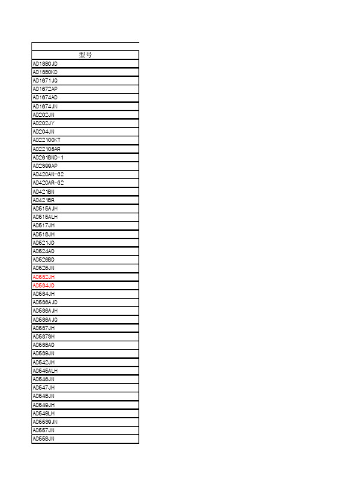
号功能简述型号AD1380JDAD1380KDAD1671JQAD1672APAD1674ADAD1674JNAD202JNAD202JYAD204JNAD22100KTAD22105ARAD261BND-1AD2S99APAD420AN-32AD420AR-32AD421BNAD421BRAD515AJHAD515ALHAD517JHAD518JHAD521JDAD524ADAD526BDAD526JNAD532JHAD534JDAD534JHAD536AJDAD536AJHAD536AJQAD537JHAD537SHAD538ADAD539JNAD542JHAD545ALHAD546JNAD547JHAD548JNAD549JHAD549LHAD5539JNAD557JNAD558JNAD568JQ AD569JN AD570JD/+ AD574AJD AD574AKD AD578KN AD580JH AD580LH AD581JH AD582KD AD584JH AD584JN AD585AQ AD586JN AD586JQ AD586KN AD586KQ AD586KR AD587KN AD587KR AD588AQ AD589JH AD590JH AD590KH AD592AN AD592BN AD595AD AD595AQ AD598AD AD600XN AD602JN AD603AQ AD606JN AD607ARS AD620AN AD621AN AD622AN AD623AN AD623AR AD624AD AD625JN AD625KN AD626AN AD627AN AD629AN AD630JNAD636JDAD636JHAD637JQAD648JNAD650JNAD650KNAD652AQAD654JNAD654JRAD660ANAD6640AST AD6644AST AD667JNAD667KNAD669ANAD670JNAD676JDAD676JNAD676KDAD677ARAD677JDAD677JNAD678JDAD678KNAD679JNAD679KNAD680JNAD684JQAD693AQAD694AQAD694JNAD698APAD7008AP20 AD7008JP-50 AD704JNAD705JNAD706JNAD707AQAD707JNAD708AQAD708JNAD7111ABN AD7111LN AD711AQAD711JNAD711JRAD712JN AD713BQ AD713JN AD720JP AD7224KN AD7226KN AD7228ABN AD722JR-16 AD7237AAN AD7237JN AD7243AN AD7245AAN AD7249BN AD724JR AD73360AR AD734AQ AD736JN AD737AQ AD737JN AD7416AR AD741KN AD743JN AD744JN AD745JN AD75019JP AD7501JN AD7502JN AD7502KQ AD7503JN AD7506JN AD7507JN AD7510DIJN AD7510DIKN AD7512DIJN AD7512DIKN AD7520LN AD7523JN AD7524JN AD7528JN AD7528KN AD7533JN AD7535JN AD7537JN AD7541AKN AD7542JN AD7543KNAD7564BN AD7574JN AD7590DIKN AD7660AST AD7664AST AD767JNAD768ARAD7701AN AD7703AN AD7703BN AD7705BN AD7705BR AD7706BN AD7707BR AD7710AN AD7711AN AD7712AN AD7713AN AD7714AN-3 AD7714AN-5 AD7715AN-5 AD7715AR-5 AD7731BN AD7741BN AD7742BN AD7750AN AD7755AARS AD7777AR AD779JDAD780ANAD781JNAD7820KN AD7821KN AD7822BN AD7824BQ AD7824KN AD7837AN AD7845JN AD7846JN AD7847AN AD7856AN AD7862AN-10 AD7864AS-1 AD7865AS-1 AD7872AN AD7874ANAD7886JD AD7886KD AD7888AR AD7890AN-10 AD7891AP-1 AD7892AN-1 AD7895AN-10 AD790JNAD795JNAD797ANAD797ARAD8001AN AD8002AN AD8009AR AD8011AN AD8015AR AD8018AR AD8031AN AD8032AN AD8036AN AD8037AN AD8041AN AD8041AR AD8042AN AD8044AN AD8047AN AD8055AR AD8056AR AD8058AR AD8079AR AD8108AST AD8109AST AD810ANAD8111AST AD8115AST AD8116AST AD811ANAD811JRAD812ANAD812ARAD8131AR AD8138AR AD813ANAD813AR-14 AD815AYAD8170ANAD817ANAD8180AN AD8184AN AD818ANAD820ANAD822ANAD822AN-3V AD823ANAD824ANAD826ANAD827AQAD827JNAD828ANAD829JNAD8307AN AD8307AR AD8309ARU AD830ANAD830ANAD8313ARM AD8313ARM AD8320ARP AD834JNAD8350AR15 AD835ANAD8402AN-10 AD8403AN100 AD840JNAD843AQAD844ANAD845JNAD845KNAD847AQAD847JNAD847SQAD849JNAD8522AN AD8551AR AD8552AR AD8561AN AD8561AR AD8564AN AD8598AN AD9042AST AD9048JQ AD9049BRSAD9051BRSAD9057BRS-40 AD9057BRS-60 AD9058JJAD9059BRSAD9066JRAD9071BRAD9101ARAD9200ARSAD9203ARUAD9220ARAD9221ARAD9223ARAD9225ARAD9226ARSAD9240ASAD9243ASAD9260ASAD9280ARSAD9281ARSAD9283BRS-100 AD9283BRS-80 AD9288BRS-80 AD9300KQAD9483KS-100 AD9500BQAD9501JNAD9617JRAD9617JNAD9618JNAD9630ANAD9631ANAD96687BQAD9698KNAD9708ARUAD9709ASTAD9713BANAD9721BRAD9731BRAD9732BRSAD9750ARAD9752ARAD9760ARAD9762ARAD9764ARAD976CNAD976AAN AD9772AST AD977AAN AD977AN AD9801JCST AD9802JST AD9803JST AD9805JS AD9816JS AD9822JR AD9830AST AD9831AST AD9832BRU AD9850BRS AD9851BRS AD9852AST AD9852ASQ AD9853AS AD9854AST AD9854ASQ AD9901KQ ADG201AKN ADG201HSJN ADG211AKN ADG222AKN ADG333ABN ADG333ABR ADG408BN ADG409BN ADG411BN ADG417BN ADG419BN ADG431BN ADG436BN ADG441BN ADG442BN ADG506AKN ADG507AKN ADG508AKN ADG508FBN ADG509AKN ADG511BN ADG608BN ADG609BN ADG719BRM ADG736BRMADM690ANADM708ANADSP21060KS160 ADSP21060CZ-160 ADSP21062KS-160 ADSP2181KS-133 ADSP2181KST-133 ADUC812BS ADVF32KNADXL105JQC ADXL202AQC AMP02FPAMP04FPDAC08CPDAC8228FPOP07AZ/883COP07CPOP07CSOP176GPOP177GPOP27GPOP291GPOP295GPOP296GPOP297GPOP297GSOP37EPOP37GPOP495GPOP497GPOP77GPOP90GPOP97FPOP97FSPKD01FPREF02CPREF03GPREF192GPREF192GSREF194GPREF195GSREF43FZSMP04EPSMP08FPSSM2141PSSM2142PSSM2211P SSM2275P TMP03FS TMP04FS TMP36GT9 MAX038CPP MAX1044CPA MAX110ACPE MAX110BCPE MAX111BCPE MAX122BCNG MAX1232CPA MAX1242BCSA MAX125CEAX MAX134CPL MAX135CPI MAX139CPL MAX140CPL MAX1480BCPI MAX1480BEPI MAX1483CPA MAX1487CPA MAX1487ECPA MAX1488ECPD MAX1489ECPD MAX148BCPP MAX1490BCPG MAX158BCPI MAX1771CPA MAX1771CSA MAX180CCPL MAX186CCPP MAX187BCPA MAX189CCPA MAX191BCNG MAX192BCPP MAX197BCNI MAX202CPE MAX202CSE MAX202ECPE MAX202EESE MAX202EPE MAX207CNG MAX208CNG MAX232CPE MAX232CSEMAX235CPG MAX238CNG MAX238ENG MAX260BCHG MAX260BENG MAX261BCNG MAX280CPA MAX291CPA MAX292CPA MAX293CPA MAX294CPA MAX297CPA MAX301CPE MAX305EPE MAX306CPI MAX3080CPD MAX3082CPA MAX308CPE MAX309CPE MAX3100CPD MAX312CPE MAX313CPE MAX318CPA MAX319CPA MAX3218CPP MAX3223CPP MAX3232CPE MAX325CPA MAX333CPP MAX338CPE MAX339CPE MAX351CPE MAX354CPE MAX354CWE MAX354EPE MAX355CPE MAX355CWE MAX366CPA MAX367CPN MAX384CPN MAX391CPE MAX400CPA MAX4016ESA MAX4100ESA MAX4101ESA MAX4106ESAMAX4142ESD MAX4146ESD MAX419CPD MAX420CPA MAX427CPA MAX435CPD MAX436CPD MAX440CPI MAX441CPP MAX442CPA MAX4456CPL MAX453EPA MAX457EPA MAX458CPL MAX468CPE MAX470CPE MAX479CPD MAX480EPA MAX483CPA MAX485CPA MAX487CPA MAX487ECPA MAX487EEPA MAX488CPA MAX490ECPA MAX491CPD MAX491ECPD MAX501AENG MAX504CPD MAX505BCNG MAX506CPP MAX509BCPE MAX512CPD MAX515CPA MAX517BCPA MAX518BCPA MAX526DCNG MAX527DCNG MAX528CPP MAX530BCNG MAX531BCPD MAX532BCPE MAX536BCWE MAX538BCPA MAX543ACPA MAX551ACPAMAX619CPA MAX6225ACPA MAX6225AESA MAX6225BCPA MAX6225BCSA MAX622CPA MAX6250BCPA MAX633ACPA MAX638AEPA MAX639CPA MAX660CPA MAX662ACPA MAX667CPA MAX691ACPE MAX691CPE MAX705CPA MAX706CPA MAX708CPA MAX708CSA-T MAX709LEPA MAX712CPE MAX712EPE MAX713CPE MAX7219CNG MAX7219ENG MAX724CCK MAX726CCK MAX729CCK MAX730ACPA MAX733CPA MAX735CPA MAX736CPD MAX738ACPA MAX738AEPA MAX739CPD MAX739CWE MAX7400CPA MAX743CPE MAX743EPE MAX749CPA MAX750ACPA MAX756CPA MAX761CPA MAX764CPA MAX765CPA MAX766EPAMAX791CPE MAX807LCPE MAX810LEUR-T MAX813LCPA MAX813LEPA MAX818LCPA MAX860ISA MAX865EUA MAX866ESA MAX874EPA MAX875BCPA MAX882CPA MAX883CPA MAX883CSA MAX907CPA MAX910CNG MAX912CPE MAX913CPA MAX931CPA MAX934CPE MXD1210CPA LFC2LFC3LFC4LFC54LFC75F003F004(5G23)F005F006F007(5G24)F010F011F1550F1490F1590F157/AF253F741(F007)F741AF747OP-07OP111AF4741F101A/201AF301AF308F110/210 F310F118/218 F441F318F124/224 F324F148F248/348 F158/258 F358F1558F4558LF791LF4136 FD37/FD38 FD46LF082 LFOP37LF3140LF7650LZ1606LZ19001 LBMZ1901 LM741LM747OP-07LM101/201 LM301LM108/208 LM308LM110LM310LM118/218 LM318LM124/224 LM324LM148LM248/348 LM158/258 LM358LM1558 OP-27CP TL062TL072TL082TL084MC1458LF147/347LF156/256/356LF107/307LF351LF353LF155/355LF157/357LM359LM381CA3080CA3100CA3130CA3140CA3240CA3193CA3401MC3303MC3403LF411LF444µpc4558MC4741LM709LM725LM733LM748ICL7650ICL7660稳压器固定输出(正电压)稳压器78xx 系列 3端稳压器 5V 到 24V1A78Lxx 系列 3端稳压器 5V 到 24V 0.1A78Mxx 系列 3端稳压器 5V 到 24V 0.5A78Sxx 系列 3端稳压器 5V 到 24V 2A固定输出(负电压)稳压器79xx 系列 3端负电压稳压器 -5V 到 -24V 1A [110kb] 79Lxx 系列 3端负电压稳压器 -5V 到 -24V 0.1A [95kb]可调输出 - 常用稳压器LM117 1.2V... 37V 1.5A 正电压可调稳压器 [100kb] LM217 1.2V... 37V 1.5A 正电压可调稳压器 [100kb] LM317 1.2V... 37V 1.5A 正电压可调稳压器 [100kb] LM137 -1.2V...-37V 1.5A 负电压可调稳压器 [246kb] LM237 -1.2V...-37V 1.5A 负电压可调稳压器 [246kb]LM337 -1.2V...-37V 1.5A 负电压可调稳压器 [246kb] LM138 1.2V --32V 5-安培 可调LM338 1.2V -- 32V 5-安培 可调LM723 高精度可调 [136kb]L200 2 A / 2.85 to 36 V.可调 [166KB]TTL 逻辑电路 [LS - HC 或 HCT 系列]74LS0074LS0474LS0874LS1074LS1374LS1474LS2774LS3074LS3274LS4274LS4574LS4774LS9074LS9274LS9374LS12174LS15474LS19274LS19374HC23774LS37474LS390CMOS 逻辑电路4001400240074011401340164017402240234025402640284029404040464051405240534055 4056 4060 4066 4067 4068 4069 4071 4072 4075 4081 4082 4093 4511 4518 4583 4584晶体管小功率管2N9302N16132N2222A 2N34392N34402N39042N39062N54012N54152N54162N55502N55512N65152N49212N49222N4923 AF125 BC107 BC108 BC109 BC148 BC177 BC178 BC179 BC182 BC183 BC184BC214BC327BC301BC302BC303BC304BC328BC337BC338BC414BC416BC461BC516BC517BC546BC547BC548BC549BC550BC556BC557BC558BC559BC560BC635BC636BC637BC638BC639BC640BCY70BCY71BCY78BCY79BCY87BCY88BCY89MPSL01 MPSL51 MPSA06 MPSA42 MPSA43 MPSA56 MPSA92 MPSA93中、大功率管2N6283 2N6284 2N6286 2N6287 BD135 BD136 BD137 BD138 BD139 BD140 BD162 BD203 BD204 BD241C BD242C BD243 BD249 BD250 BD375 BD376 BD377 BD378 BD379 BD380 BD543 BD529 BD530 BD533 BD534 BD535 BD536 BD537 BD538 BD677 BD678 BD679 BD680 BD681 BD682 BD591 BD592 BDX53C BDX54C BDW51 BU208A BU508AMJ2955MJ4502MJ15003MJ15004MJE340MJE350MJE15028MJE15029MJE15030MJE15031PMD16K100PMD17K100TIP31TIP32TIP122TIP140TIP141TIP142TIP145TIP146TIP147TIP2955TIP3055Fet 晶体管2N52482N54572N5460BS170BF245CBF256BJ210J211J212Fet 功率管2SK15302SJ201IRF540IRF9540集成电路(模拟)AD711CA3130LH0032LF351LF411LM108LM208LM833LM358LM359LM324LM391LM393NE5532NE5534OP27OP37TL071TL072TL074TL081TL082TL084TLC271TLC272TLC274MN3004IC's 功率放大 [模拟] L165LM388LM1875TDA1516BQTDA1519CTDA1563QTDA2002TDA2005TDA2004TDA2030STK4036 IISTK4036 XISTK4038 IISTK4040 IISTK4040 XISTK4042 IISTK4042 XISTK4044 IISTK4044 IISTK4046 XISTK4048 XISTK4050 V显示驱动LM3914LM3915UAA180CA3161ECA3162EICL7136PLL 立体声解码LM1800CA3090PMC1310P定时-时钟电路555556MN3101XR2206光电耦合4N254N264N274N284N354N364N37H11A1H11A2H11A3SCR - TRIAC BTY79-800RC106D时钟MM5314N二极管1N4000 系列1N41481N5408IN5236B1N5240B1N5252B电子管300B5U4G6SN76BX76DJ8ECC886N1PECC88692212AT712AU712AX7E80CCECC81ECC82ECC83ECC88EL34EL84Z2CKT88常用锁相环电路集成电路型号(规格) 数据表生产厂家器件名称参考单价兼容型号EM92600/1EMC 专用型锁相环(中国10频道)HT9286A/BHT9287A/BHOLTEK 专用型锁相环(美国10频道)HT9288A/BHOLTEK 专用型锁相环(中国10频道)HYL21011S/JHYUNDAI 通用型锁相环HYL21012S/JHYUNDAI 专用型锁相环(美国10频道)HYL21014S/JHYUNDAI 专用型锁相环(中国10频道)MC145162MOTOROLA通用型锁相环MC145166MOTOROLA专用型锁相环(美国10频道)MC145167MOTOROLA专用型锁相环(美国10频道)KS8805BGM6532LG 专用型锁相环(中国10频道)DMD5603DAEWOO专用型锁相环(中国10频道)DMD5602DAEWOO专用型锁相环(美国10频道)KA567KA567LLM567常用元器件ICL7106,ICL7107DAC0830/DAC0832ADC0831/ADC0832/ADC0834/ADC0838 ADC0808/ADC0809ADC0802/ADC0803/ADC0804AD7520/AD7521/AD7530/AD75214N35/4N36/4N37ICL7116,ICL7117ICL7650ICL7660/MAX1044ICL7106,ICL7107DAC0830/DAC0832ADC0831/ADC0832/ADC0834/ADC0838 ADC0808/ADC0809ADC0802/ADC0803/ADC0804AD7520/AD7521/AD7530/AD75214N35/4N36/4N37ICL7116,ICL7117ICL7650ICL7660/MAX1044ICL8038ICM7216ICM7226ISO2-CMOSLF351LF353LM117/LM317A/LM317LM124/LM124/LM324LM137/LM337LM139/LM239/LM339LM158/LM258/LM358LM193/LM293/LM393LM201/LM301LM231/LM331LM285/LM385LM308ALM386LM399LM431LM567/LM567CLM741LM831LM833LM8365MAX038MC1403MC1404MC1413/MC1416MC145026/MC145027/MC145028MC145403-5/8MC145406MC145407MC145583MC145740MC1488MC1489MC2833MC3362MC4558MC7800系列MC78L00系列MC78M00系列MC78T00系列MC7900系列MC79L00系列MC79M00系列Microchip PIC系列单片机RS232通讯应用MM5369MOC3009/MOC3012MOC3020/MOC3023MOC3081/MOC3082/MOC3083MOC8050MOC8111MT8870MT8888CNE5532/NE5532ANE5534/SE5534NE555/SA555NE556/SA556/SE556NE570/NE571/SA571OP07OP27OP37OP77OP90PC817/PC827/PC847PT2262PT2272SG2524/SG3524ST7537TDA1521TDA7000TTDA7010TTDA7021TTDA7040TTDA7050TL062/TL064TL071/TL072/TL074TL082/TL084 JFETTL494TL594TLP521/1-4TOP100-4TOP221-7TOP232-4TOP412/TOP414ULN2068ULN2803ULN2803/ULN2804VFC32LM319LM393/LM339经典8腿IC封装(LM393)经典14腿IC封装(LM339)电源范围 2――36V静态工作电流 0.4mA翻转时间 1.3us最大输出电流 16mA输入电压范围 -0.3V――Vcc型号功能简述功能16位 20us高性能模数转换器(民用级)16位 20us高性能模数转换器(民用级)12位 1.25MHz采样速率带宽2MHz模数转换器(民用级)12位 3MHz采样速率带宽20MHz单电源模数转换器(工业级)12位 100KHz采样速率带宽500KHz模数转换器(工业级)12位 100KHz采样速率带宽500KHz模数转换器(民用级)小型2KHz隔离放大器(民用级)卧式小型2KHz隔离放大器(民用级)立式小型5KHz隔离放大器(民用级)卧式带信号调理比率输出型温度传感器可编程温控开关电阻可编程温度控制器 SOIC数字隔离放大器可编程正弦波振荡器(工业级) PLCC16位单电源 4-20mA输出数模转换器(工业级)DIP16位单电源 4-20mA输出数模转换器(工业级)SOIC16位环路供电符合HART协议 4-20mA输出数模转换器(工业级)DIP 16位环路供电符合HART协议 4-20mA输出数模转换器(工业级)SOIC 低价格,低偏置电流,高输入阻抗运放(民用级) TO-99低价格,低偏置电流,高输入阻抗运放(民用级) TO-99低失调电压,高性能运放 (民用级) TO-99宽带,低价格运放(民用级) TO-99电阻设置增益精密仪表放大器(民用级)DIP引脚设置增益高精度仪表放大器(工业级)DIP软件编程仪表放大器(工业级)DIP软件编程仪表放大器(民用级)DIP模拟乘法器(民用级)TO-99模拟乘法器(民用级)DIP模拟乘法器(民用级)TO-99集成真有效值直流转换器(民用级)DIP集成真有效值直流转换器(民用级)TO-99集成真有效值直流转换器(民用级)DIP150KHZ集成压频转换器(民用级)TO-99150KHZ集成压频转换器(军用级)TO-99单片实时模拟乘法器(工业级)DIP宽带双通道线性乘法器(民用级)DIP低价格,低偏置电流,高输入阻抗运放(民用级) TO-99低偏置电流,高输入阻抗运放(民用级) TO-99静电计放大器(民用级)DIP低价格,低偏置电流,高输入阻抗运放(民用级) TO-99精密 BiFET输入运放(民用级)DIP低偏置电流,高输入阻抗运放(民用级) TO-99低偏置电流,高输入阻抗运放(民用级) TO-99高速运放(民用级)DIP微处理器兼容完整7位电压输出数模转换器(民用)DIP微处理器兼容完整8位电压输出数模转换器(民用)DIP12位 0.25us电流输出数模转换器(民用)DIP12位超高速电流输出数模转换器(民用)DIP16位 3us电流输出数模转换器(民用)DIP8位 25us模数转换器(民用)DIP12位 25us模数转换器(民用)DIP12位 25us模数转换器(民用)DIP12位 3us模数转换器(民用)DIP精密 2.5V电压基准源(民用级)TO-52精密 2.5V电压基准源(民用级)TO-52精密 10V电压基准源(民用级)TO-50.7us采样保持放大器(民用)DIP引脚设置输出电压基准源(民用级)TO-99引脚设置输出电压基准源(民用级)DIP3us采样保持放大器(工业级)DIP精密 5V电压基准源(民用级)DIP精密 5V电压基准源(民用级)DIP精密 5V电压基准源(民用级)DIP精密 5V电压基准源(民用级)DIP精密 5V电压基准源(民用级)SOIC精密 10V电压基准源(民用级)DIP精密 10V电压基准源(民用级)SOIC精密可编程电压基准源(工业级)DIP精密 1.235V电压基准源(民用级)H-02A—55℃~150℃测温范围温度传感器 TO-52—55℃~150℃测温范围温度传感器 TO-52低价格,精密单片温度传感器 TO-92低价格,精密单片温度传感器 TO-92K型(铬-铝)热电偶信号调节器(工业级)DIPK型(铬-铝)热电偶信号调节器(工业级)DIP线性可变位移信号调节器(LVDT)(工业级)DIP低噪声宽带可变增益双运放(民用级)DIP低噪声宽带可变增益双运放(民用级)DIP低噪声可变增益运放(工业级)DIP50MHz, 80db对数放大器(民用级)DIP低功耗混频器/AGC/RSSC 3V接收机的IF子系统(工业级) SSOP 低功耗仪表放大器(工业级)DIP低功耗仪表放大器(工业级)DIP单电源仪表放大器(工业级)DIP单电源Rail-Rail输出仪表放大器(工业级)DIP单电源Rail-Rail输出仪表放大器(工业级)SOIC精密仪表放大器(工业级)DIP可编程增益仪表放大器(民用级)DIP可编程增益仪表放大器(民用级)DIP单电源仪表放大器(工业级)DIP单电源低功耗Rail-Rail输出仪表放大器(工业级)DIP高电压抑制比差分放大器(工业级) DIP平衡跳制解调器(民用级)DIP低价格模拟乘法器(民用级)DIP高精度真有效值直流转换器(民用级)DIP高精度真有效值直流转换器(民用级)TO-99高精度真有效值直流转换器(民用级)DIP精密,BiFET输入运放(民用级)DIP1MHz,电压频率转换器(民用级)DIP1MHz,电压频率转换器(民用级)DIP2MHz,同步电压频率转换器(工业级)DIP500KHz,低价格电压频率转换器(民用级)DIP500KHz,低价格电压频率转换器(民用级)SOIC16位 8us串并行输入数模转换器(工业级)DIP12位65MSPS模数转换器(工业级) LQFP14位65MSPS模数转换器(工业级) LQFP12位 3us并行输入数模转换器(民用级)DIP12位 3us并行输入数模转换器(民用级)DIP16位 8us并行输入数模转换器(工业级)DIP单电源,内带仪表放大器电压基准源8位数模转换器(民用级)DIP16位100KSPS采样速率并行输出模数转换器(民用级)DIP16位100KSPS采样速率并行输出模数转换器(民用级)DIP16位100KSPS采样速率并行输出模数转换器(民用级)DIP16位100KSPS采样速率串行输出模数转换器(民用级)SOIC16位100KSPS采样速率串行输出模数转换器(民用级)DIP16位100KSPS采样速率串行输出模数转换器(民用级)DIP12位200KSPS采样速率并行输出模数转换器(民用级)DIP12位200KSPS采样速率并行输出模数转换器(民用级)DIP14位128KSPS采样速率并行输出模数转换器(民用级)DIP14位128KSPS采样速率并行输出模数转换器(民用级)DIP精密 2.5V电压基准源(民用级)DIP1us 四通道采样保持放大器(民用级)DIP环路供电,4~20mA输出传感器信号变送器(工业级)DIP0~2V或0~10V输入,4~20mA或0-20mA输出信号变送器(工业级)DIP 0~2V或0~10V输入,4~20mA或0-20mA输出信号变送器(民用级)DIP 通用线性可变位移信号调节器(LVDT)(工业级)PLCC带10位D/A,20MHz主频直接数字同步调制器(工业级)PLCC带10位D/A,50MHz主频直接数字同步调制器(民用级)PLCC精密四运放(民用级)DIP精密运放(民用级) DIP精密双运放(民用级) DIP精密单运放(工业级)DIP精密单运放(民用级)DIP双AD707(工业级)DIP双AD707(民用级)DIP0.37db对数数模转换器(工业级)DIP0.37db对数数模转换器(工业级)DIP精密 BiFET输入运放(工业级)DIP精密 BiFET输入运放(民用级)DIP精密 BiFET输入运放(民用级)SOIC双AD711(工业级)DIP双AD711(民用级)DIP四AD711(工业级)DIP四AD711(民用级)DIPRGB-NTSC/PAL编码器(民用级)PLCC8位 3us转换时间电压输出数模转换器(民用级)DIP8位 4通道3us转换时间电压输出数模转换器(民用级)DIP8位 8通道5us转换时间电压输出数模转换器(工业级)DIPAnalog toNTSC/PAL编码器(民用级) SOIC12位 2通道5us转换时间电压输出数模转换器(工业级)DIP12位 2通道5us转换时间电压输出数模转换器(民用级)DIP12位电压输出型数模转换器(工业级) DIP12位 10us转换时间电压输出数模转换器(工业级)DIP12位双路串行输出数模转换器(工业级) DIPAnalog toNTSC/PAL编码器(民用级) SOIC16位6通道数据采集子系统(三相电量测量IC)(工业级) SOIC10MHz带宽四象限模拟乘法器(工业级)DIP通用真有效值直流转换器(民用级)DIP通用真有效值直流转换器(工业级)DIP通用真有效值直流转换器(民用级)DIP片内带D/A 数字输出温度传感器 LM35升级品可8片级联(工业级)SOIC 通用运放(民用级)DIP低噪声,BiFET输入运放(民用级)DIP精密,双极性运放(民用级)DIP精密低噪声运放(民用级) DIP16×16音频距阵开关(民用级) PLCC8选1 CMOS多路转换器(民用级)DIP差动4选1 CMOS多路转换器(民用级)DIP差动4选1 CMOS多路转换器(民用级)DIP8选1 CMOS多路转换器(民用级)DIP16选1 CMOS多路转换器(民用级)DIP差动8选1 CMOS多路转换器(民用级)DIP四单刀单掷 CMOS介质隔离模拟开关9民用级)DIP四单刀单掷 CMOS介质隔离模拟开关9民用级)DIP双单刀双掷 CMOS介质隔离模拟开关9民用级)DIP双单刀双掷 CMOS介质隔离模拟开关9民用级)DIP10位 CMOS数模转换器(民用级)DIP8位 CMOS数模转换器(民用级)DIP8位 CMOS带锁存数模转换器(民用级)DIP8位 180ns电流输出CMOS数模转换器(民用级)DIP8位 180ns电流输出CMOS数模转换器(民用级)DIP10位 600ns电流输出CMOS数模转换器(民用级)DIP14位 1.5us电流输出CMOS数模转换器(民用级)DIP12位双路1.5us电流输出CMOS数模转换器(民用级)DIP12位 600ns电流输出CMOS数模转换器(民用级)DIP12位 250ns电流输出CMOS数模转换器(民用级)DIP12位串行输入CMOS数模转换器(民用级)DIP12位 1us电流输出CMOS数模转换器(民用级)DIP低功耗四路数模转换器(工业级) DIP8位 15us电流输出CMOS数模转换器(民用级)DIP四单刀单掷 CMOS带锁存介质隔离模拟开关9民用级)DIP16位100KSPS CMOS模数转换器(工业级) LQFP16位570KSPS CMOS模数转换器(工业级) LQFP12位高速电压输出数模转换器(民用级)DIP16位高速电流输出数模转换器(民用级)SOIC16位 ∑–△模数转换器(工业级)DIP20位 ∑–△模数转换器(工业级)DIP20位 ∑–△模数转换器(工业级)DIP16位 ∑–△模数转换器(工业级)DIP16位 ∑–△模数转换器(工业级)SOIC16位 ∑–△模数转换器(工业级)DIP16位 ∑–△模数转换器(工业级)SOIC24位 ∑–△模数转换器(工业级)DIP24位 ∑–△模数转换器(工业级)DIP24位 ∑–△模数转换器(工业级)DIP24位 ∑–△模数转换器(工业级)DIP24位 ∑–△模数转换器(工业级)DIP 3V电源24位 ∑–△模数转换器(工业级)DIP 5V电源16位 ∑–△模数转换器(工业级)DIP 5V电源16位 ∑–△模数转换器(工业级)SOIC 5V电源24位 ∑–△模数转换器(工业级)DIP单通道输入6MHz压频转换器(工业级) DIP四通道输入6MHz压频转换器(工业级) DIP两通道乘积/频率转换器电度表专用芯片(工业级)DIPIEC521/1036标准电度表专用芯片(工业级)DIP10位多路T/H子系统(工业级) SOIC14位128KSPS采样速率并行输出模数转换器(民用级)DIP2.5V或3V可选输出高精度电压基准源(工业级)DIP700ns采样保持放大器(民用级)DIP8位500KSPS采样速率模数转换器(民用级)DIP8位1MSPS采样速率模数转换器(民用级)DIP8位2MSPS采样速率模数转换器(工业级)DIP8位四通道高速模数转换器(民用级)DIP8位四通道高速模数转换器(工业级)DIP12位双路乘法数模转换器(工业级)DIP12位乘法数模转换器(民用级)DIP16位电压输出数模转换器(民用级)DIP12位双路乘法数模转换器(工业级)DIP14位8通道285KSPS采样速率模数转换器(工业级)DIP12位4通道同时采样250KSPS速率模数转换器带2SHA and 2ADCs(工业级)DIP 12位4通道同时采样147KSPS速率模数转换器(工业级)PQFP14位4通道同时采样175KSPS速率模数转换器带2SHA and 2ADCs(工业级)PQFP 14位串行输出模数转换器(工业级)DIP12位 750KSPS采样速率模数转换器(民用级)DIP12位8通道200KSPS速率模数转换器(工业级)SOIC12位单电源八通道串行采样模数转换器(工业级)DIP12位单电源八通道串并行采样模数转换器(工业级)DIP12位600KSPS采样模数转换器(工业级)DIP12位单电源200KSPS采样速率模数转换器(工业级)DIP12位四通道同时采样模数转换器(工业级)DIP12位四通道同时采样模数转换器(工业级)SOIC12位 750KSPS采样速率模数转换器(民用级)DIP高速精密比较器(民用级)DIP低偏置电流低噪声运放(民用级)DIP低失真低噪声运放(工业级)DIP低失真低噪声运放(工业级)SOIC800MHz 电流反馈运放(工业级)DIP800MHz 电流反馈双运放(工业级)DIP1GHz 4500V/us 电流反馈双运放(工业级)DIP340MHz 电流反馈运放(工业级)DIP单电源真空管前置放大器(工业级) SOIC5V Rail-Rail 大电流输出 XDSL线性驱动放大器(工业级) SOIC 单电源 Rail-Rail输入输出运放(工业级)DIP单电源 Rail-Rail输入输出双运放(工业级)DIP低失真宽带240MHz电压输出运放(工业级)DIP低失真宽带270MHz电压输出运放(工业级)DIP120MHz带宽 Rail-Rail输出运放(工业级)DIP120MHz带宽 Rail-Rail输出运放(工业级)SOIC120MHz带宽 Rail-Rail输出双运放(工业级)DIP80MHz带宽 Rail-Rail输出四运放(工业级)DIP电压反馈运放(工业级) DIP电压反馈运放(工业级) SOIC低价格 300MHz电压反馈双运放(工业级) SOIC电压反馈双运放(工业级) SOIC双通道 260MHz缓冲器(工业级) SOIC8×8视频距阵开关(工业级) LQFP8×8视频距阵开关(工业级) LQFP带电源休眠控制端的低功耗视频运放(工业级) DIP16×8视频距阵开关(工业级) LQFP16×16视频距阵开关(工业级) LQFP16×16视频距阵开关(工业级) LQFP高性能视频运放(工业级) DIP高性能视频运放(工业级) SOIC低功耗电流反馈双运放(工业级) DIP低功耗电流反馈双运放(工业级) SOIC差分输入输出电压反馈放大器(工业级) SOICIF 放大器(工业级) SOIC单电源低功耗三视频运放(工业级) DIP单电源低功耗三视频运放(工业级) SOIC大电流输出,差动输入\输出运放(工业级)2选1视频多路转换器(工业级) DIP4选1视频多路转换器(工业级) DIP高速低功耗宽电源运放(工业级) DIP差动2选1视频多路转换器(工业级) DIP4选1视频多路转换器(工业级) DIP低价格高速电压反馈视频运放(工业级) DIP单电源低功耗FET输入 Rail-Rail输出运放(工业级) DIP 双AD820(工业级) DIP双AD820(工业级) DIP 3V电源单电源 Rail-Rail输出双运放(工业级) DIP单电源 Rail-Rail输出四运放(工业级) DIP高速低功耗双运放(工业级) DIP双AD847 (工业级) DIP双AD847 (民用级) DIP双AD818(工业级) DIP高速低噪声视频运放(工业级) DIP500MHz对数放大器(工业级)DIP500MHz对数放大器(工业级)SOIC500MHz对数放大器(工业级)TSSOP高速视频差动运放(工业级) DIP高速视频差动运放(工业级) DIP2.5GHz对数放大器(工业级) RM-82.5GHz对数放大器(工业级) RM-8数字可变增益线性驱动器(工业级) RP-20500MHz带宽四象限模拟乘法器(工业级)DIP差分输入射频放大器(工业级) SOIC250MHz带宽四象限电压输出模拟乘法器(工业级)DIP2通道数字电位器阻值10K(工业级) DIP4通道数字电位器阻值100K(工业级) DIP宽带高速运放(民用级) DIP34MHz带宽高速FET输入运放(工业级) DIP2000V/us高速运放(工业级) DIP16MHz带宽高速FET输入运放(民用级) DIP16MHz带宽高速FET输入运放(民用级) DIP300V/us高速低功耗运放(工业级) DIP300V/us高速低功耗运放(民用级) DIP300V/us高速低功耗运放(军用级) DIP高速低功耗运放(民用级) DIP12 位单电源双路电流输出型数模转换器(工业级) DIP 自稳零运放(工业级) SOIC自稳零双运放(工业级) SOIC单电源比较器(工业级)DIP单电源比较器(工业级) SOIC单电源TTL/CMOS四路比较器(工业级) DIP单电源双路比较器(工业级) DIP12位41MSPS模数转换器(工业级) LQFP8位35MSPS视频模数转换器(民用级) DIP9位30MSPS模数转换器(工业级) SSOP10位40MSPS模数转换器(工业级) SOIC10位60MSPS模数转换器(工业级) SSOP8位40MSPSz视频模数转换器(工业级) SSOP8位60MSPS视频模数转换器(工业级) SSOP双路8位50MSPS视频模数转换器(民用级) LCC双路8位60MSPS视频模数转换器(工业级) SSOP双路6位60MSPS视频模数转换器(民用级) SSOP10位TTL兼容100MSPS模数转换器(工业级) SOIC7ns建立时间采样保持放大器(工业级) SOIC10位20MSPS模数转换器(工业级) SSOP10位40MSPS模数转换器(工业级) TSSOP12位10MSPS模数转换器(工业级) SOIC12位1MSPS模数转换器(工业级) SOIC12位3MSPS模数转换器(工业级) SOIC12位25MSPS模数转换器(工业级) SOIC12位65MSPS模数转换器(工业级) SSOP14位10MSPS模数转换器(工业级) MQFP14位3MSPS模数转换器(工业级) MQFP16位2.5MSPS∑–△模数转换器(工业级)MQFP单电源8位32MSPS模数转换器(工业级) SSOP单电源 8位双路32MSPS模数转换器(工业级) SSOP单电源8位100MSPS模数转换器(工业级) SSOP单电源8位80MSPS模数转换器(工业级) SSOP单电源 8位双路80MSPS模数转换器(工业级) SSOP4选1宽带视频多路转换器(民用级) DIP8位 100MSPS三视频模数转换器(民用级)MQFP数字化可编程延迟信号发生器(工业级) DIPTTL/COMS数字化可编程延迟信号发生器(民用级) DIP 1400V/us,140MHz带宽高速运放(民用级) SOIC1400V/us,140MHz带宽高速运放(民用级) DIP1800V/us,160MHz带宽高速运放(民用级) DIP低失真闭环缓冲放大器(工业级) DIP超低失真宽带电压反馈放大器(工业级) DIP高速双电压比较器(工业级) DIP高速TTL兼容双电压比较器(工业级) DIP8位100MSPS 双路数模转换器(工业级) TSSOP8位125MSPS 双路数模转换器(工业级) PQFP12位 80MSPS TTL兼容数模转换器(工业级) DIP10位 400MSPS TTL兼容数模转换器(工业级) SOIC10位 170MSPS 双电源数模转换器(工业级) SOIC10位 200MSPS 单电源数模转换器(工业级) SSOP10位125MSPS 数模转换器(工业级) SOIC12位125MSPS 数模转换器(工业级) SOIC10位100MSPS 数模转换器(工业级) SOIC12位100MSPS 数模转换器(工业级) SOIC14位100MSPS 数模转换器(工业级) SOIC16位100KSPS BiCMOS并行输出模数转换器(工业级) DIP16位100KSPS BiCMOS并行输出模数转换器(工业级) DIP16位200KSPS BiCMOS并行输出模数转换器(工业级) DIP14位300MSPS 数模转换器(工业级) LQFP16位200KSPS BiCMOS串行输出数模转换器(工业级) DIP16位100KSPS BiCMOS串行输出数模转换器(工业级) DIP10位 6MSPS CCD信号处理器(民用级)LQFP10位 6MSPS CCD信号处理器(民用级)LQFP10位 6MSPS CCD信号处理器(民用级)LQFP10位 3通道 6MSPS CCD信号处理器(民用级) MQFP12位 3通道 6MSPS CCD信号处理器(民用级) MQFP14位 3通道 12MSPS CCD信号处理器(民用级) SOIC带10位D/A,25MHz主频直接数字同步调制器(工业级)PQFP带10位D/A,50MHz主频直接数字同步调制器(工业级)PQFP带10位D/A,25MHz主频直接数字同步调制器(工业级)TSSOP带10位D/A,125MHz主频直接数字同步调制器(工业级)SSOP带10位D/A,180MHz主频直接数字同步调制器(工业级)SSOP带12位D/A,200MHz主频直接数字同步调制器(工业级)LQFP-80带散热器带12位D/A,300MHz主频直接数字同步调制器(工业级)LQFP-80数字 QPSK/16 QAM 调整器(工业级) PQFP带12位D/A,200MHz主频直接数字同步调制器(工业级)LQFP-80带散热器带12位D/A,300MHz主频直接数字同步调制器(工业级)LQFP-80线性相位探测器/频率鉴别器(民用级) DIP四单刀单掷模拟开关(民用级) DIP四单刀单掷模拟开关(民用级) DIP四单刀单掷模拟开关(民用级) DIP四单刀单掷模拟开关(民用级) DIP四单刀单掷模拟开关(工业级) DIP四单刀单掷模拟开关(工业级) SOIC8选1CMOS模拟多路转换器(工业级) DIP差动4选1CMOS模拟多路转换器(工业级) DIP四单刀单掷模拟开关(工业级) DIP单刀单掷模拟开关(工业级) DIP单刀单掷模拟开关(工业级) DIP四单刀单掷模拟开关(工业级) DIP双单刀单掷模拟开关(工业级) DIP四单刀单掷模拟开关(工业级) DIP四单刀单掷模拟开关(工业级) DIP16选1CMOS模拟多路转换器(民用级) DIP差动8选1CMOS模拟多路转换器(民用级) DIP8选1CMOS模拟多路转换器(民用级) DIP8选1CMOS带过压保护模拟多路转换器(工业级) DIP差动4选1CMOS模拟多路转换器(民用级) DIP单电源四单刀单掷模拟开关(工业级) DIP8选1CMOS模拟多路转换器(工业级) DIP差动4选1CMOS模拟多路转换器(工业级) DIP单路视频CMOS模拟开关(工业级)RM-6双路视频CMOS模拟开关(工业级)RM-10DC-DC转换器(工业级)DIP微处理器监控电路(工业级) DIP微处理器监控电路(工业级) DIP32位浮点数字信号处理器内存4M(民用级)PQFP32位浮点数字信号处理器内存4M(工业级)PQFP32位浮点数字信号处理器内存2M(民用级)PQFP16位定点数字信号处理器(民用级)PQFP-12816位定点数字信号处理器(民用级)TQFP-128带单片机、8路12位A/D、2路D/A的数采系统(工业级)PQFP 500KHz工业标准压频转换器(民用级) DIP±1g-±5g带温度补偿加速度传感器(民用级)QC-14±2g双路加速度传感器(工业级)QC-14高精度仪表放大器(工业级) DIP单电源精密仪表放大器(工业级) DIP8位高速电流输出型数模转换器(民用级) DIP8位双路电压输出型数模转换器(工业级) DIP超低失调电压运放(军用级)DIP超低失调电压运放(工业级)DIP超低失调电压运放(工业级)SOIC低失真低噪声运放(工业级)DIP高精密运放(工业级) DIP低噪声精密运放(工业级) DIP单电源 Rail-Rail输入输出双运放(工业级)DIP单电源 Rail-Rail输入输出双运放(工业级)DIP微功耗 Rail-Rail输入输出双运放(工业级)DIP超低偏置电流精密双运放(工业级) DIP超低偏置电流精密双运放(工业级) SOIC低噪声精密运放(民用级) DIP低噪声精密运放(工业级) DIP单电源 Rail-Rail输入输出四运放(工业级)DIP超低偏置电流精密四运放(工业级) DIPOP07改进型(工业级) DIP低电压微功耗精密运放(工业级) DIP微功耗精密运放(工业级) DIP微功耗精密运放(工业级) SOIC峰值检测器(工业级) DIP精密5V电压基准源带温度传感器(工业级) DIP精密低价格2.5V电压基准源(工业级) DIP低功耗大电流输出2.5V电压基准源(工业级) DIP低功耗大电流输出2.5V电压基准源(工业级) SOIC低功耗大电流输出4.5V电压基准源(工业级) DIP低功耗大电流输出5V电压基准源(工业级) SOIC高精度2.5V电压基准源(工业级)DIP7us四通道采样保持放大器(工业级) DIP7us八通道采样保持放大器(工业级) DIP差动线路接收器 Gain=0dB(工业级) DIP平衡线路驱动器(工业级) DIP差动线路接收器 Gain=-6dB(工业级) DIP1W功率差分输出音频功率放大器(工业级)DIPRail-Rail输出双音频功率放大器(工业级)DIPPWM输出,直接与微处理器接口数字输出温度传感器 SOIC反相PWM输出,直接与微处理器接口数字输出温度传感器 SOIC 电压输出温度传感器 TO-92波形发生器60KHz振荡器自举模式DC-DC 电荷泵转换器低价格双路14位串形模数转换器低价格双路14位串形模数转换器低价格14位串形模数转换器高速带采保和基准的12位模数转换器微处理器监控电路10位带2.5V基准的串形模数转换器14位2×4通道4路同时采集并行模数转换器积分型A/D转换器,+5V,3-3/4位低功率A/D转换器积分型A/D转换器积分型A/D转换器完全隔离半双RS-485接口完全隔离半双RS-485接口RS-485/RS-442接口,256个节点RS-485/RS-442接口,128个节点RS-485/RS-442接口,+15KV保护RS-232接口,+15KV保护RS-232接口,+15KV保护低功耗8路10位A/D完全隔离全双IKS-485接口高速8路8位A/D开关型DC-DC变换器开关型DC-DC变换器8路12位A/D串行接口A/D,带采保,电压基准,12位,采样速率133KHZ串行A/D,12位,采样速率75KHZ低功耗,12位单通道,串行带采保和电压基准A/D低功耗,12位单通道,带采保和电压基准A/D串行A/D,10位采样速率133M12位,八通道故障保护,带采保并行A/DRS-232接口,+5VRS-232接口+15KV静电保护RS-232接口+15KV静电保护,工业级RS-232接口工业级RS-232接口RS-232接口RS-232接口RS-232接口,+5VRS-232接口工业级RS-232接口RS-232接口5组收发器RS-232接口RS-232接口双路,开关电容型4阶滤波器双路,开关电容型4阶滤波器双路,开关电容型4阶滤波器单路,开关电容型5阶滤波器有源滤波器,时钟可编程有源滤波器,时钟可编程有源滤波器,时钟可编程有源滤波器,时钟可编程有源滤波器,时钟可编程模拟开关模拟开关模拟多路转换器失效保护RS-485/RS-232失效保护RS-485/RS-232模拟多路转换器模拟多路转换器通用异步收发信机(UART)模拟开关模拟开关模拟开关模拟开关RS-232接口RS-232接口RS-232接口模拟开关模拟开关模拟多路转换器模拟多路转换器模拟开关模拟多路转换器模拟多路转换器模拟多路转换器(工业级)模拟多路转换器模拟多路转换器模拟多路转换器模拟多路转换器模拟多路转换器模拟多路转换器运算放大器视频放大器视频放大器视频放大器视频放大器。
康佳电视故障解决方法大全
电视维修实例康佳T953PD彩色电视机整机三无,按遥控开关键,红灯闪亮即灭,但不开机微处理控制电路V405的Ub为0.45V,V405发射结开路康佳T953PD彩色电视机图像正常,伴音小且有很大的干扰声伴音鉴频电路T103失效康佳T953PD彩色电视机声图均有,但图像右边有约3cm的黑边行锯齿波积分电路RP304变值康佳T953PD彩色电视机图像中的上部稀疏,只有下部10cm的垂直黑边场反馈输入电路N301的27脚电压为6.8V,C448漏电康佳T953PD彩色电视机收看中不定时关机,重新开机有时不能启动,此时指示灯闪烁或熄灭电源电路D401活动片断裂康佳T953PD彩色电视机三无,指示灯亮,启动机器时红灯熄灭,开关机瞬间有咕声电源;电路TA7698的33脚电压为8.4V,R363开路康佳T953PD彩色电视机开机三无,红指示灯亮一下后常亮遥控电路TLP621损坏康佳T953PD彩色电视机有伴音,光栅暗,色度对比度,亮度失控亮度通道电路D301短路康佳T953PD彩色电视机正常收看突然无像无声,屏幕有正常的噪波点高频头电路RF AGC电压为5.V7,C119漏电康佳T953PD彩色电视机自动搜索时各频段不停地循环,搜到节目后,画\面淡且一闪而过节目信号识别电路V609的Ub这0.04V,R658虚焊康佳T953PD彩色电视机每次开机或更换频道时均需要重新调谐才能选出正常的电视节目存储器电路N602的12脚与601的34脚的连接铜箔断裂康佳T953PD彩色电视机绿色字符显示为黑色字符字符显示电路C345两端电压为0V,R352变值康佳T953PD彩色电视机伴音失控ATT电路TA7680AP的1脚电压在3.5V且有变化,V608击穿康佳T953PD彩色电视机U频收不到节目调谐电压电路CPU的1脚电压在H段搜索结束时, 不能从0V转为5V,CPU的1脚内U段电路损坏康佳T953PD彩色电视机自动搜台不能锁定AFC电路当搜到画面时,TA7680AAP的13脚电压为6.3V,R676开路康佳T953PD彩色电视机能搜台,但不能存储,换频道后,原来预置好的电视节目消失,必须重复预置存储电路M5868SP的2脚无-30V电压,M5865SP损坏康佳T953PD彩色电视机预置好的电视节目10分钟后消失调谐电压电路V101击穿康佳T953PD彩色电视机不能自动搜台,屏幕无字符显示自动搜台的键盘电路S605损坏康佳T953彩色电视机黑白图像及伴音正常,但图像无彩色解码电路N301的7脚电压为1.1V,不随色饱和度的增减而变化,N601损坏康佳T953彩色电视机伴音失真并有杂音,但图像无彩伴音电路L604失谐康佳T953彩色电视机音量失控,其它各功能正常音量控制电路IC602损坏康佳T953彩色电视机开启电源后无任何反应遥控电源电路T401电压为0V,T401的保险丝熔断康佳T953彩色电视机开机无光,无音,电源灯亮,遥控不起作用电源电路C403两端电压为20V,电源开关组件下面的红色纸片漏电康佳T953彩色电视机收看中突然无声无像,屏幕有正常的噪波RFAGC电路RFAGC电压为5.7V,C119漏电康佳T953彩色电视机U段接收正常,V段无图无声VHF电压控制Q606 Uc正常为11.5V,R628开路康佳T953彩色电视机无光无声,无字符显示,指示灯随开关而亮灭行扫描电路行回扫变压器因高压击穿,并烧坏偏转线圈康佳T953彩色电视机图像上有虚线斜条,且斜条飘忽不定场输出电路C453漏电康佳T953彩色电视机图象模糊,伴音失真中放电路N101的11脚电压为5.25V,C119漏电康佳T953彩色电视机开机正常,一会变为白光成A V状态图像通道电路N101的15脚电压为4V,5脚电压为6.8V,C116失效康佳T953彩色电视机绿色字符显示为黑色字符,节目不能存储,转换频道后,原电视节目消失,必须重复预置存储器电路N602的12脚无电压,R352开路康佳T953彩色电视机伴音换控伴音电路V608击穿康佳T953彩色电视机U段收不到节目微处理电路N601在H段搜索时不能从0V转为5V,N601损坏康佳T953彩色电视机自动搜台锁不住AFT电路N101的13脚电压在 6.36V上下摆动,V604击穿康佳T953彩色电视机电视节目10分钟左右消失高频头调谐电压电路BT端电压为20.3V,V101损坏康佳T953彩色电视机在收看过程中,机内冒烟且有打火声,即三无,发出吱吱声自动亮度电路R425变值康佳T953彩色电视机整机三无,亦无字符显示,按遥控电源键时,红灯亮过压保护电路V305的Uc为0.6V,R426开路康佳T953彩色电视机整机三我,屏幕无显示,待命灯亮时钟脉冲电路N601的28,29脚无脉冲,Z601漏电康佳T953彩色电视机通电后,面板上的红灯亮,但整机三无,亦无字符显示待命电源电路N60117脚电压为4.6V,R669变值,C611漏电康佳T953P彩色电视机开机工作一段时间后,机器突然无光无声,关机后一会又能重新开机,但故障又重复保护电路VD301失效康佳T953P彩色电视机开机工作一段时间后,机器突然无光无声,关机后一会又能重新开机,但故障又重复取样电路RP401不良康佳T953P彩色电视机电源灯亮,按遥控器开机键,电源灯灭,电视机无光无声可控硅保护电路V407开路康佳T953P彩色电视机接通电源开关,电源灯不亮辅助电源电路VD403负端无16V电压,VD401也无-30V电压,遥控变压器开路康佳T953P彩色电视机图像模糊且有回扫线行扫描电路C455漏电康佳T953P彩色电视机屏幕上有色斑消磁电路T401损坏康佳T953P彩色电视机图像模糊,伴音失控AGC电路N101的(11)脚电压为0.5V(正常为5.25V),C119漏电康佳T953P彩色电视机无光栅,无伴音,无字符显示, 按遥控器的开/关机键,面板上红指示灯能亮灭,但不能开机行扫描电路V405的Ub为2V(正常为0.45V),V405击穿康佳T953P彩色电视机黑白图像基本正常,但无彩色,伴音较小且噪声大中频前置放大电路SA101损坏康佳T953P彩色电视机一条水平亮线. 场扫描电路IC401的(3)'(6)脚无电压,R431断路. 康佳T953P彩色电视机开机"三无",且伴有"嘟嘟"声一条水平亮线行扫描电路+B无电压输出.C420漏电.康佳T953P彩色电视机开机2分钟后行失步,关机后再开机,故障重现AFC电路C343(0.47υF/50V)容量失效.康佳T953P彩色电视机绿色字符显示为黑色字符字符显示电路R352失效康佳T953P彩色电视机U频道节目收不到频段切换电路N601的1脚电压在U段不能从0V回转为5V.N601损坏.康佳T953P彩色电视机能自动搜台,但不能锁台AGC脉冲输入电路N101的13脚电压在6.36上下摆动,C610开路失效康佳T953P彩色电视机设置好的电视节目10分钟后消失调谐电压控制电路V101不良康佳T953P彩色电视机能自动搜台,但屏幕无字符显示键盘电路S605断路康佳T953P彩色电视机音正常,图像模糊,约半小时后清晰显像管及管座显像管11脚与12脚的反向电阻为0Ω,显像管管座KB漏电康佳T953P彩色电视机伴音正常,暗无像亮度通道电路N301的8脚电压8.4V,D301短路康佳T953P彩色电视机每次开机或更换频道时均需重新调谐才能收看存储器控制电路N602的12脚与34脚断裂康佳T953P彩色电视机搜台时各频段不停地循环搜索,画面淡且一闪而过同步信号校正电路V609的Ue为0.04V,R658开路康佳T953P彩色电视机选台时只能选到部分电台,且图象不稳,无法收看调谐电压电路BP 端只能在0-24V间变化,C102漏电康佳T963A彩色电视机自动搜台时,图像在屏幕上只稳定1秒就继续搜台,节目不能锁定存储器电路IC602损坏康佳T963A彩色电视机开机一切正常,10分钟后光栅压缩行扫描电路Q402击穿康佳T963A彩色电视机伴音正常,图像清晰度模糊图像中放电路iC101的11脚电压为4.4V,C117漏电康佳T963A彩色电视机图像及伴音正常,只是关机后出现色斑消磁电路TH901开路康佳T963A彩色电视机无光,无声,无像电源电路T901损坏康佳T963A彩色电视机无光无声,无像行扫描电路IC301振荡电路坏康佳T963A彩色电视机无光,无声,无像微处理控制电路X601失效康佳T963A彩色电视机无光无音,无像开关电源电路CD901击穿康佳T963A彩色电视机图像伴音正常,光栅亮度比正常亮,同时机内有叭啦,叭啦的火花声电源电路Q901熔断康佳T963A彩色电视机出现大面积爬行且色调畸变色解码电路IC301的17,19脚电压为4V,C350漏电康佳T963A彩色电视机黑白图像正常,但无彩色;亦无伴音,自动搜索不停,且有时仍自动关机行逆程脉冲传输出电路IC301的(36)脚电压1.7V(正常为2.9V;(38)脚电压为0.3V(正常为0.6V),C303开路康佳T963A彩色电视机开机后无光栅,无伴音,待机指示灯和环绕声指示灯亮,手控,遥控全部失灵微处理控制电路C600漏电康佳T963A彩色电视机开机后无光栅,无伴音,待机指示灯和环绕声指示灯亮,手控,遥控全部失灵微处理控制电路C600漏电康佳T963A彩色电视机伴音小鉴频电路T103失谐康佳T963A彩色电视机无图无声,有浓密的噪波点中放通道电路V117漏电康佳T963A彩色电视机场线性差场扫描电路C452漏电康佳T963A彩色电视机灵敏度低中放通道电路C117漏电康佳T963A彩色电视机VHF频段节目正常,UHF频段节目收看约2小时后跑台高频头高频头损坏康佳T963A彩色电视机黑白图像着色慢且有重影色解码电路, C301的18脚电压为8.1V,R349开路康佳T963A彩色电视机字符随光栅颜色而变字符显示电路D616虚焊康佳T963A彩色电视机图像正常,无伴音伴音电路TDA2009A的6脚电压不稳,C339松动康佳T963A彩色电视机各频段搜索不停,电视画面开始时稳定,随之行失步,2秒后继续搜索AFC电路T104失调康佳T963A彩色电视机正常收看10分钟后,电视机信号丢失,满屏噪点高频头调谐供电电路R601变值康佳T963A彩色电视机自动或半自动搜台时有彩色,结束彩色丢失,黑白图像正常微处理控制电路CF8581损坏康佳T963A彩色电视机开机20分钟后光栅亮度下降,图像变淡遥控接口电路TA7698AP 稳定性差康佳T963A彩色电视机开机,整机处于预备状态,约1小时后自动开机,声图正常微处理控制电路PCA84C640的41脚电压为0V,PCA84C640损坏康佳T963A彩色电视机伴音正常,但屏幕为暗红色光栅,无图,有回扫线,字符亮度下降字符信号通路Q505的Ue由134.5V降至88V,Q610击穿康佳T963A彩色电视机声图正常,字符边界拉丝,字符颜色随画面变化而变化PCA84C640的消陷驱动电路字符显示消隐脉冲电路,C633失效康佳T963A彩色电视机声图正常,遥控时有字符显示,但字符偏左PCA84C640的RC时钟振荡电路PCA84C640的时钟振荡频率高于100MH,VR601变值康佳T963A彩色电视机彩色时深时淡且有干扰色同步脉冲检波负载滤波电路IC301的7脚电压为5.3V,C339虚焊康佳T963A彩色电视机图像正常,但无音伴音功放电路IC201的2,4脚电压为0.7V,Q204断路康佳T963A彩色电视机正常收看10分钟后,节目丢失,随即满屏噪点PCA84C640的14位D/A转换电路ZD001两端电压30V,R601增值康佳T963A彩色电视机开机20分钟后,光栅亮度下降,图像变暗亮度通道电路IC301的42脚电压为6.4V,IC301内热稳定性差康佳T963A彩色电视机光栅为一条水平亮线场扫描电路IC402损坏康佳T963A彩色电视机有音,无像行扫描电路R411变值康佳T963A彩色电视机无光无音开关电源R911开路康佳KK-T2103彩色电视机有光,无像中放通道 C120漏电康佳KK-T2103彩色电视机有像无声伴音电路IC201损坏康佳KK-T2103彩色电视机无光,无声行扫描电路Q402击穿康佳KK-T2103彩色电视机无光无声电源电路D904击穿康佳KK-T2103彩色电视机屏幕上呈现白光栅,无像,伴音正常视频放大电路TA8759BN的35脚电压正常为1.35V,D305开路康佳T2106彩色电视机屏幕暗,呈现模糊的彩色图像,但伴音和字符显示正常亮度通电路C370开路康佳T2106彩色电视机屏幕呈一条水平亮线场扫描电路TA8759BN的31脚电压为0.2V,29脚电压为0V,ZD301击穿康佳T2106彩色电视机无光栅,无图像,无伴音行扫描电路Q401的Uc为70V,C402漏电康佳T2106彩色电视机无光栅,无图像,无伴音开关电源电路+140V升至为+200V,F901熔汤康佳T2106彩色电视机图像正常,无伴,调节音量键,屏幕上的音量标志正常变化伴音中放电路IC0018-10脚电压为5.98V,C012严重漏电康佳T2106彩色电视机自动搜台锁不住节目AFT电路IC001的20脚电压为4.8V,C606漏电康佳T2106彩色电视机图像正常,遥控或手控调节音量时,屏幕能显示音量逐渐增大或减小,但仅有微弱的伴音且不随音量的调节变化电子音量衰减电路IC1101的20脚电压为4.8V,V626漏电康佳T2106彩色电视机自动和手动均不能锁台微处理控制电路IC601的51脚电压为1.91V,V608漏电康佳T2106彩色电视机图像正常,无音伴音中放电路IC001的9脚电压为0.8V,C102漏电康佳T2114彩色电视机伴音失真伴音电路Z210失效康佳T2114彩色电视机光栅呈一条水平亮线场扫描电路L405开路康佳T2114彩色电视机整机三无,无待机指示,开机有吱吱声开关电源电路V008的Ub为0V,C059击穿康佳T2506彩色电视机AGC失效,各种制式下图像和伴音均是信噪比差,调VR001无效中放电路调VR001时,同时测IC001的7脚电压无变化,IC001损坏康佳T2506彩色电视机PAL制,NTSC制和SCEAM制均无图像,无伴音中放电路IC001的1,2脚电压为5.4V,IC001损坏康佳T2506彩色电视机左声道声音小有杂音伴音功放电路IC801(TDA2009)性能不良康佳T2506彩色电视机图像上部拉长,下部严重压缩场扫描电路C426(330μF/25V)漏电康佳T2506彩色电视机无光栅,无伴音,无图像开关电源电路F901熔断;C911失效康佳T2510彩色电视机自动搜台时锁不住AFT电压电路TA8611第20脚电压为4.8V,C606漏电康佳T2510彩色电视机人正常的图像,无伴音,但调节音量键时,屏幕上的音量标志变化正常伴音功放电路YA8611第8,9脚电压为1.6V,C012漏电康佳T2510彩色电视机正常收看一段时间后,图像逐渐扭曲,伴音逐渐失真,最后节目消失,重新调台,故障重复出现电子调谐器及供电电路MN1528KWE第39脚电压为3.2V,Q619为21V,电子调谐器不良康佳T2510彩色电视机刚开机正常,工作4分钟后PAL制色色彩消失,调节色度钮无效,停机30分钟后开机又重复本故障色同步选通门电路TA8759第34脚电压为3V,C319漏电康佳T2510彩色电视机在接收中,H段突然声图皆无,但L,U频段一直正常H频段控制电路高频头第6脚电压为12V,V104虚焊康佳T2510彩色电视机开机屏幕呈很亮的光栅,数秒后光栅消失,但伴音正常亮度电路R416开路康佳T2510彩色电视机开机后无光栅,但伴音完好过压保护电路IC801第30脚电压为0V,C513漏电康佳T2510彩色电视机开机后无光栅,但伴音完好X射线保护电路TA7698AP第30脚电压为0V,C622开路康佳T2510彩色电视机无光栅,无伴音开关电源电路STR-6309击穿康佳T2512A彩色电视机AGC失控,各种制式下图像和伴音均是信噪比差,调VR001无效中频通道电路TA8411的7脚电压无变化,T8611损坏康佳T2512A彩色电视机PAL制,NTSC制SCEM制均无像,无音中频通道电路TA8611的1,2脚电压为2.6左右,TA8611损坏康佳T2512A彩色电视机图像正常,无音,只有沙沙声,噪声大小可调伴音中频通道电路T8615第12脚无波形,C104断路康佳T2512A彩色电视机字符显示正常,但手动和自动寻台时各频段无图像, 中放电路高频头第5脚电压为3.9VC003开路康佳T2512A彩色电视机伴音正常,但图像彩色时有时无PAL解码电路TA8759N 25脚电压为5.6V,C332开路康佳T2512A彩色电视机重放SECAM制节目时,屏幕全红,而其它制式节目正常SECAM色解码电路TA8759第64脚电压为7V,C346击穿康佳T2512A彩色电视机每次开机收看约10分钟,光栅变暗,遥控和手控不能调大亮度亮度信号处理电路TA8759第51脚电压为5V,C349漏电康佳T2512A彩色电视机自动搜台正常,手动搜台时无PAK屏显,无像无音搜台编码与解码电路MN15287WE第13脚电压始终为0V康佳T2512A彩色电视机图像为黑而模糊的彩色影像,调小色饱和度只有暗淡的光栅亮度电路TA8759第59脚电压为0V,TA8759损坏康佳T2512A彩色电视机光栅时有时无,行不同步同步分离电路TA8759第29脚电压为0.73V,C310短路康佳T2512A彩色电视机接收NTSC制节目时,图像的水平位置偏左行中心校正电路Q308损坏康佳T2512A彩色电视机在任何制式光栅均不满屏场锯齿波形成电路TA8759N第31脚电压为6.6V,C323不良康佳T2512A彩色电视机无伴音,只有较大的嗡嗡声中放电路C294严重漏电康佳T2512A彩色电视机三无,红灯亮电源稳压电路V901的Ub 为-2.6V,VD917击穿康佳T2512A彩色电视机开机红灯不亮,按键不起作用,有光有噪声+5V稳压电源电路N601的52脚无电压,V908击穿康佳T2512A彩色电视机开机红灯不亮,按键不起作用,有光,有雪花,有噪声,无图+5V稳压电源电路N601的52脚电压为4.95V,27脚电压为4.91V,R918开路康佳T2916A彩色电视机三无,电源灯不亮偏置电路+B电压为0V,V908击穿康佳T2916A彩色电视机三无,民源灯亮开关电源电路+B电压降到0.7V,V901的Ue为0V,R951一脚虚焊康佳T2916A彩色电视机三无,电源灯亮输出电路+B电压上升到38V即下降至0V,V402击穿康佳彩电维修1.康佳T914H三无拆机发现F402断,C443、C436爆裂,说明三无故障是由于电源电压输出过高引起的。
GE Fanuc RX3i PacSystem IC695PSA140 40W 多用途电源说明书

Rx3i PacSystem919-535-3180*******************GE Fanuc IC695PSA140/automation/ge-fanuc/rx3i-pacsystem/IC695PSA140120/240V AC, 125VDC Multipurpose Power Supply IC695P IC695PSIC695PSA4-16 PACSystems™ RX3i System Manual – October 2005 GFK-2314CMulti-Purpose Power Supply, 120/240 VAC or 125 VDC, 40 Watt: IC695PSA140Power Supply IC695PSA140 is a multi-purpose 40-Watt supply that operates from an input voltagesource in the range of 85 to 264 VAC or 100 VDC to 300 VDC.This power supply provides three outputs:■ +5.1 VDC output,■ +24 VDC relay output that can be used to powercircuits on Output Relay modules.■ +3.3 VDC. This output is used internally by RX3imodules with IC695 catalog numbers.This Power Supply is suitable for use in load-sharing and redundancy applications. Up to 4 Multi-purpose power supplies (PSA140 and/or PSD140) can be used in a PACSystems RX3i (IC695 catalog number) Universal Backplane. Use these Power Supplies if the number of modules required exceeds the capacity of one Power Supply. This Power Supply occupies two backplane slots.The Power Supply indicates when an internal fault occurs so the CPU can detect loss of power or log the appropriate fault code.CautionThis Power Supply cannot be used with RX3i IC695PSD040 or IC695PSA040 Power Supplies in redundant or increased capacity modes. Damage to equipment may result.POWER P/S FAULTGFK-2314C Chapter 4 Power Supplies 4-17LEDsFour LEDs on the Power Supply indicate:■ Power (Green/Amber). When this LED isgreen, it indicates power is being suppliedto the backplane. When this LED is amber, power is applied to the Power Supply but the Power Supply switch is off.■ P/S Fault (Red). When this LED is lit, itindicates the Power Supply has failed and is no longer supplying sufficient voltage to the backplane.■ Over Temperature (Amber). When this LEDis lit, it indicates the Power Supply is near or exceeding its maximum operating temperature.■ Overload (Amber). When this LED is lit, itindicates the Power Supply is near orexceeding its maximum output capability on at least one of its outputs.The CPU Fault Table shows a fault if any Overtemperature, Overload, or P/S Fault occurs.On/Off SwitchThe ON/OFF switch is located behind the door on the front of the module. The switch controls the operation of the outputs of the supply. It does NOT interrupt line power. Projecting tabs next to the switch help prevent accidentally turning it on or off.Wiring TerminalsTerminals for power, ground, and MOV disconnect accept individual 14 to 22 AWG wires. PO W ER P/S F AULT4-18 PACSystems™ RX3i System Manual – October 2005 GFK-2314CSpecifications: IC695PSA140Nominal Rated Voltage Input Voltage Range AC DC120/240 VAC or 125 VDC85 to 264 VAC 100 to 300 VDC Input Power(Maximum with Full Load)70 Watts maximumInrush Current 4 Amps, 250 milliseconds maximum * Output Power40 Watts maximum total5.1 VDC = 30 Watts maximum 3.3 VDC = 30 Watts maximumThe maximum total output power available depends on the ambient temperature, as shown.Output Voltage24 VDC: 19.2 VDC to 28.8 VDC5.1 VDC: 5.0 VDC to 5.2 VDC (5.1 VDC nominal) 3.3 VDC: 3.1 VDC to 3.5 VDC (3.3 VDC nominal)Output Current24 VDC: 0 to 1.6 Amps 5.1 VDC: 0 to 6 Amps 3.3 VDC: 0 to 9 AmpsIsolation (input to backplane): 250 VAC continuous; 1500 VAC for 1 minute Ripple (all outputs) 150 mV Noise (all outputs) 150 mVRide-through time20 ms. This is the length of time the Power Supply maintains valid outputs if the power source is interruptedWiring Terminals Each terminal accepts one 14 AWG to 22 AWG wire. Current per Terminal 6 Amps Number of Daisy-Chained PSA140 SuppliesUp to 4 Number of PSA140 Power Supplies in Universal BackplaneUp to 4* The Inrush Current specification is given as a guide for sizing the external powersource for the IC695PSA140. Peak inrush current may be higher for shorter durations.WarningThe power supply’s door must be closed. During normal operation with an AC power source either 120 VAC or 240 VAC is present on the AC Power Supply. The door protects against accidental shock hazard that could cause severe or fatal injury to personnel.Thermal Deratings: PSA140The maximum output power for Power Supply PSA140 depends on the ambient temperature, as shown below.GFK-2314C Chapter 4 Power Supplies 4-194-20 PACSystems™ RX3i System Manual – October 2005 GFK-2314COvercurrent ProtectionThe 5.1 VDC output is electronically limited to 7 Amps. The 3.3 VDC output is limited to 10 Amps. If an overload (including short circuits) occurs, it is sensed internally and the Power Supply shuts down. Because it is designed for redundancy applications, this Power Supply latches “OFF” in fault conditions and will not automatically try to restart until the overloadcondition is removed. Input power must be cycled to clear a latched fault. However, if the Power Supply is used in a non-redundant application where automatic restarting is required, a jumper plug can be installed.An internal fusable linke in the input line is provided as a backup. The Power Supply usually shuts down before the fusable linke blows. The fusable linke also protects against internal supply faults. The CPU Fault Table shows a fault if any Overtemperature, Overload, or P/S Fault occurs. There is no additional indication if the Power Supply fusable linke blows.In a non-redundancy application, where automatic restarting is may be appropriate, a shunt can be installed on back of the module as shown at left. The shunt must have 0.100 inch spacing on center and accommodate 0.25 inch pins. Example parts are Radio Shack DIP Programming Shunt #276-1512 and DIGI-Key #59000-ND. The module must be removed from the backplane to install the shunt.Field Wiring: IC695PSA140Power Source and Ground ConnectionsThe wires from the power source and ground connect to the terminals on the Power Supply as shown at right. Each terminal accepts one AWG 14 to AWG 22 wire.WarningIf the same external AC power source is used to provide power to two or more RX3i power supplies in the system, connection polarity must be identical at each power supply. A resulting difference in potential can injure personnel or cause damage to equipment.Also, each backplane must be connected to acommon system ground.GFK-2314C Chapter 4 Power Supplies 4-21Input Overvoltage ProtectionThe bottom terminal is normally connected toframe ground with a user-installed jumper as shown lower right. If overvoltage protection is not required or is supplied upstream, no jumper is needed.To Hi-pot test this supply, overvoltage protection must be disabled during the test by removing the jumper. Re-enable overvoltage protection after testing by reinstalling the jumper.In systems with a floating neutral input (the neutral line is not referenced to Protective Earth Ground), this jumper must NOT be installed. In addition, in a floating neutral system, voltage surge protection devices such as MOVs must be installed from L1 to earth ground, and from L2 (Neutral) to earth ground.。
常用开关电源芯片大全之欧阳育创编

常用开关电源芯片大全第1章DC-DC电源转换器/基准电压源1.1 DC-DC电源转换器1.低噪声电荷泵DC-DC电源转换器AAT3113/AAT31142.低功耗开关型DC-DC电源转换器ADP30003.高效3A开关稳压器AP15014.高效率无电感DC-DC电源转换器FAN56605.小功率极性反转电源转换器ICL76606.高效率DC-DC电源转换控制器IRU30377.高性能降压式DC-DC电源转换器ISL64208.单片降压式开关稳压器L49609.大功率开关稳压器L4970A10.1.5A降压式开关稳压器L497111.2A高效率单片开关稳压器L497812.1A高效率升压/降压式DC-DC电源转换器L597013.1.5A降压式DC-DC电源转换器LM157214.高效率1A降压单片开关稳压器LM1575/LM2575/LM2575HV15.3A降压单片开关稳压器LM2576/LM2576HV16.可调升压开关稳压器LM257717.3A降压开关稳压器LM259618.高效率5A开关稳压器LM267819.升压式DC-DC电源转换器LM2703/LM270420.电流模式升压式电源转换器LM273321.低噪声升压式电源转换器LM275022.小型75V降压式稳压器LM500723.低功耗升/降压式DC-DC电源转换器LT107324.升压式DC-DC电源转换器LT161525.隔离式开关稳压器LT172526.低功耗升压电荷泵LT175127.大电流高频降压式DC-DC电源转换器LT176528.大电流升压转换器LT193529.高效升压式电荷泵LT193730.高压输入降压式电源转换器LT195631.1.5A升压式电源转换器LT196132.高压升/降压式电源转换器LT343333.单片3A升压式DC-DC电源转换器LT343634.通用升压式DC-DC电源转换器LT346035.高效率低功耗升压式电源转换器LT346436.1.1A升压式DC-DC电源转换器LT346737.大电流高效率升压式DC-DC电源转换器LT378238.微型低功耗电源转换器LTC175439.1.5A单片同步降压式稳压器LTC187540.低噪声高效率降压式电荷泵LTC191141.低噪声电荷泵LTC3200/LTC3200-542.无电感的降压式DC-DC电源转换器LTC325143.双输出/低噪声/降压式电荷泵LTC325244.同步整流/升压式DC-DC电源转换器LTC340145.低功耗同步整流升压式DC-DC电源转换器LTC340246.同步整流降压式DC-DC电源转换器LTC340547.双路同步降压式DC-DC电源转换器LTC340748.高效率同步降压式DC-DC电源转换器LTC341649.微型2A升压式DC-DC电源转换器LTC342650.2A两相电流升压式DC-DC电源转换器LTC342851.单电感升/降压式DC-DC电源转换器LTC344052.大电流升/降压式DC-DC电源转换器LTC344253.1.4A同步升压式DC-DC电源转换器LTC345854.直流同步降压式DC-DC电源转换器LTC370355.双输出降压式同步DC-DC电源转换控制器LTC373656.降压式同步DC-DC电源转换控制器LTC377057.双2相DC-DC电源同步控制器LTC380258.高性能升压式DC-DC电源转换器MAX1513/MAX151459.精简型升压式DC-DC电源转换器MAX1522/MAX1523/MAX152460.高效率40V升压式DC-DC电源转换器MAX1553/MAX155461.高效率升压式LED电压调节器MAX1561/MAX159962.高效率5路输出DC-DC电源转换器MAX156563.双输出升压式DC-DC电源转换器MAX1582/MAX1582Y64.驱动白光LED的升压式DC-DC电源转换器MAX158365.高效率升压式DC-DC电源转换器MAX1642/MAX164366.2A降压式开关稳压器MAX164467.高效率升压式DC-DC电源转换器MAX1674/MAX1675/MAX167668.高效率双输出DC-DC电源转换器MAX167769.低噪声1A降压式DC-DC电源转换器MAX1684/MAX168570.高效率升压式DC-DC电源转换器MAX169871.高效率双输出降压式DC-DC电源转换器MAX171572.小体积升压式DC-DC电源转换器MAX1722/MAX1723/MAX172473.输出电流为50mA的降压式电荷泵MAX173074.升/降压式电荷泵MAX175975.高效率多路输出DC-DC电源转换器MAX180076.3A同步整流降压式稳压型MAX1830/MAX183177.双输出开关式LCD电源控制器MAX187878.电流模式升压式DC-DC电源转换器MAX189679.具有复位功能的升压式DC-DC电源转换器MAX194780.高效率PWM降压式稳压器MAX1992/MAX199381.大电流输出升压式DC-DC电源转换器MAX61882.低功耗升压或降压式DC-DC电源转换器MAX62983.PWM升压式DC-DC电源转换器MAX668/MAX66984.大电流PWM降压式开关稳压器MAX724/MAX72685.高效率升压式DC-DC电源转换器MAX756/MAX75786.高效率大电流DC-DC电源转换器MAX761/MAX76287.隔离式DC-DC电源转换器MAX8515/MAX8515A88.高性能24V升压式DC-DC电源转换器MAX872789.升/降压式DC-DC电源转换器MC33063A/MC34063A90.5A升压/降压/反向DC-DC电源转换器MC33167/MC3416791.低噪声无电感电荷泵MCP1252/MCP125392.高频脉宽调制降压稳压器MIC220393.大功率DC-DC升压电源转换器MIC229594.单片微型高压开关稳压器NCP1030/NCP103195.低功耗升压式DC-DC电源转换器NCP1400A96.高压DC-DC电源转换器NCP140397.单片微功率高频升压式DC-DC电源转换器NCP141098.同步整流PFM步进式DC-DC电源转换器NCP142199.高效率大电流开关电压调整器NCP1442/NCP1443/NCP1444/NCP1445100.新型双模式开关稳压器NCP1501101.高效率大电流输出DC-DC电源转换器NCP1550102.同步降压式DC-DC电源转换器NCP1570103.高效率升压式DC-DC电源转换器NCP5008/NCP5009 104.大电流高速稳压器RT9173/RT9173A105.高效率升压式DC-DC电源转换器RT9262/RT9262A106.升压式DC-DC电源转换器SP6644/SP6645107.低功耗升压式DC-DC电源转换器SP6691108.新型高效率DC-DC电源转换器TPS54350109.无电感降压式电荷泵TPS6050x110.高效率升压式电源转换器TPS6101x111.28V恒流白色LED驱动器TPS61042112.具有LDO输出的升压式DC-DC电源转换器TPS6112x 113.低噪声同步降压式DC-DC电源转换器TPS6200x114.三路高效率大功率DC-DC电源转换器TPS75003115.高效率DC-DC电源转换器UCC39421/UCC39422116.PWM控制升压式DC-DC电源转换器XC6371117.白光LED驱动专用DC-DC电源转换器XC9116118.500mA同步整流降压式DC-DC电源转换器XC9215/XC9216/XC9217119.稳压输出电荷泵XC9801/XC9802120.高效率升压式电源转换器ZXLB16001.2 线性/低压差稳压器121.具有可关断功能的多端稳压器BAXXX122.高压线性稳压器HIP5600123.多路输出稳压器KA7630/KA7631124.三端低压差稳压器LM2937125.可调输出低压差稳压器LM2991126.三端可调稳压器LM117/LM317127.低压降CMOS500mA线性稳压器LP38691/LP38693128.输入电压从12V到450V的可调线性稳压器LR8129.300mA非常低压降稳压器(VLDO)LTC3025130.大电流低压差线性稳压器LX8610131.200mA负输出低压差线性稳压器MAX1735132.150mA低压差线性稳压器MAX8875133.带开关控制的低压差稳压器MC33375134.带有线性调节器的稳压器MC33998135.1.0A低压差固定及可调正稳压器NCP1117136.低静态电流低压差稳压器NCP562/NCP563137.具有使能控制功能的多端稳压器PQxx138.五端可调稳压器SI-3025B/SI-3157B139.400mA低压差线性稳压器SPX2975140.五端线性稳压器STR20xx141.五端线性稳压器STR90xx142.具有复位信号输出的双路输出稳压器TDA8133143.具有复位信号输出的双路输出稳压器TDA8138/TDA8138A144.带线性稳压器的升压式电源转换器TPS6110x145.低功耗50mA低压降线性稳压器TPS760xx146.高输入电压低压差线性稳压器XC6202147.高速低压差线性稳压器XC6204148.高速低压差线性稳压器XC6209F149.双路高速低压差线性稳压器XC64011.3 基准电压源150.新型XFET基准电压源ADR290/ADR291/ADR292/ADR293151.低功耗低压差大输出电流基准电压源MAX610x152.低功耗1.2V基准电压源MAX6120153.2.5V精密基准电压源MC1403154.2.5V/4.096V基准电压源MCP1525/MCP1541155.低功耗精密低压降基准电压源REF30xx/REF31xx156.精密基准电压源TL431/KA431/TLV431A第2章AC-DC转换器及控制器1.厚膜开关电源控制器DP104C2.厚膜开关电源控制器DP308P3.DPA-Switch系列高电压功率转换控制器DPA423/DPA424/DPA425/DPA4264.电流型开关电源控制器FA13842/FA13843/FA13844/FA138455.开关电源控制器FA5310/FA53116.PWM开关电源控制器FAN75567.绿色环保的PWM开关电源控制器FAN76018.FPS型开关电源控制器FS6M07652R9.开关电源功率转换器FS6Sxx10.降压型单片AC-DC转换器HV-2405E11.新型反激准谐振变换控制器ICE1QS0112.PWM电源功率转换器KA1M088013.开关电源功率转换器KA2S0680/KA2S088014.电流型开关电源控制器KA38xx15.FPS型开关电源功率转换器KA5H0165R16.FPS型开关电源功率转换器KA5Qxx17.FPS型开关电源功率转换器KA5Sxx18.电流型高速PWM控制器L499019.具有待机功能的PWM初级控制器L599120.低功耗离线式开关电源控制器L659021.LINK SWITCH TN系列电源功率转换器LNK304/LNK305/LNK30622.LINK SWITCH系列电源功率转换器LNK500/LNK501/LNK52023.离线式开关电源控制器M51995A24.PWM电源控制器M62281P/M62281FP25.高频率电流模式PWM控制器MAX5021/MAX502226.新型PWM开关电源控制器MC4460427.电流模式开关电源控制器MC4460528.低功耗开关电源控制器MC4460829.具有PFC功能的PWM电源控制器ML482430.液晶显示器背光灯电源控制器ML487631.离线式电流模式控制器NCP120032.电流模式脉宽调制控制器NCP120533.准谐振式PWM控制器NCP120734.低成本离线式开关电源控制电路NCP121535.低待机能耗开关电源PWM控制器NCP123036.STR系列自动电压切换控制开关STR8xxxx37.大功率厚膜开关电源功率转换器STR-F665438.大功率厚膜开关电源功率转换器STR-G865639.开关电源功率转换器STR-M6511/STR-M652940.离线式开关电源功率转换器STR-S5703/STR-S5707/STR-S570841.离线式开关电源功率转换器STR-S6401/STR-S6401F/STR-S6411/STR-S6411F 442.开关电源功率转换器STR-S651343.离线式开关电源功率转换器TC33369~TC3337444.高性能PFC与PWM组合控制集成电路TDA16846/TDA1684745.新型开关电源控制器TDA1685046.“绿色”电源控制器TEA150447.第二代“绿色”电源控制器TEA150748.新型低功耗“绿色”电源控制器TEA153349.开关电源控制器TL494/KA7500/MB375950.Tiny SwitchⅠ系列功率转换器TNY253、TNY254、TNY25551.Tiny SwitchⅡ系列功率转换器TNY264P~TNY268G52.TOP Switch(Ⅱ)系列离线式功率转换器TOP209~TOP22753.TOP Switch-FX系列功率转换器TOP232/TOP233/TOP23454.TOP Switch-GX系列功率转换器TOP242~TOP25055.开关电源控制器UCX84X56.离线式开关电源功率转换器VIPer12AS/VIPer12ADIP57.新一代高度集成离线式开关电源功率转换器VIPer53第3章功率因数校正控制/节能灯电源控制器1.电子镇流器专用驱动电路BL83012.零电压开关功率因数控制器FAN48223.功率因数校正控制器FAN75274.高电压型EL背光驱动器HV8265.EL场致发光背光驱动器IMP525/IMP5606.高电压型EL背光驱动器/反相器IMP8037.电子镇流器自振荡半桥驱动器IR21568.单片荧光灯镇流器IR21579.调光电子镇流器自振荡半桥驱动器IR215910.卤素灯电子变压器智能控制电路IR216111.具有功率因数校正电路的镇流器电路IR216612.单片荧光灯镇流器IR216713.自适应电子镇流器控制器IR252014.电子镇流器专用控制器KA754115.功率因数校正控制器L656116.过渡模式功率因数校正控制器L656217.集成背景光控制器MAX8709/MAX8709A18.功率因数校正控制器MC33262/MC3426219.固定频率电流模式功率因数校正控制器NCP165320.EL场致发光灯高压驱动器SP440321.功率因数校正控制器TDA4862/TDA486322.有源功率因数校正控制器UC385423.高频自振荡节能灯驱动器电路VK05CFL24.大功率高频自振荡节能灯驱动器电路VK06TL第4章充电控制器1.多功能锂电池线性充电控制器AAT36802.可编程快速电池充电控制器BQ20003.可进行充电速率补偿的锂电池充电管理器BQ20574.锂电池充电管理电路BQ2400x5.单片锂电池线性充电控制器BQ2401xB接口单节锂电池充电控制器BQ2402x7.2A同步开关模式锂电池充电控制器BQ241008.集成PWM开关控制器的快速充电管理器BQ29549.具有电池电量计量功能的充电控制器DS277010.锂电池充电控制器FAN7563/FAN756411.2A线性锂/锂聚合物电池充电控制器ISL629212.锂电池充电控制器LA5621M/LA5621V13.1.5A通用充电控制器LT157114.2A恒流/恒压电池充电控制器LT176915.线性锂电池充电控制器LTC173216.带热调节功能的1A线性锂电池充电控制器LTC173317.线性锂电池充电控制器LTC173418.新型开关电源充电控制器LTC198019.开关模式锂电池充电控制器LTC400220.4A锂电池充电器LTC400621.多用途恒压/恒流充电控制器LTC400822.4.2V锂离子/锂聚合物电池充电控制器LTC405223.可由USB端口供电的锂电池充电控制器LTC405324.小型150mA锂电池充电控制器LTC405425.线性锂电池充电控制器LTC405826.单节锂电池线性充电控制器LTC405927.独立线性锂电池充电控制器LTC406128.镍镉/镍氢电池充电控制器M62256FP29.大电流锂/镍镉/镍氢电池充电控制器MAX150130.锂电池线性充电控制器MAX150731.双输入单节锂电池充电控制器MAX1551/MAX155532.单节锂电池充电控制器MAX167933.小体积锂电池充电控制器MAX1736B接口单节锂电池充电控制器MAX181135.多节锂电池充电控制器MAX187336.双路输入锂电池充电控制器MAX187437.单节锂电池线性充电控制器MAX189838.低成本/多种电池充电控制器MAX190839.开关模式单节锂电池充电控制器MAX1925/MAX192640.快速镍镉/镍氢充电控制器MAX2003A/MAX200341.可编程快速充电控制器MAX712/MAX71342.开关式锂电池充电控制器MAX74543.多功能低成本充电控制器MAX846A44.具有温度调节功能的单节锂电池充电控制器MAX8600/MAX860145.锂电池充电控制器MCP73826/MCP73827/MCP7382846.高精度恒压/恒流充电器控制器MCP73841/MCP73842/MCP73843/MCP73844 647.锂电池充电控制器MCP73861/MCP7386248.单节锂电池充电控制器MIC7905049.单节锂电池充电控制器NCP180050.高精度线性锂电池充电控制器VM7205。
长虹维修资料

长虹维修资料长虹维修资料-技改-高压包代换-CPU代换-维修实例LT4019P\LT4028配自制电源GP03或GP03-1时,部分机器的电源组件会产生低频约160HZ的噪声,针对此现象,可作如下更改改善噪声:首先,取消主板上的贴片电阻R206、R204;然后,在稳压器件U206的输出端(+3.3V)与贴片电阻R204的非地端连接飞线(也可选择与它等电位点连接,如C219的非地端、JP201或JP202的第2脚)。
另外,也可用外购电源FSP277-4F01直接替换GP03或GP03-1,这样主板就可不做任何更改。
换下的电源可用于其他使用此电源的机型。
也可以直接将R206改为900欧(680欧+220欧)LT4019P:GP03或GP03-1电源啸叫的处理办法:1.将ZB板上R204、R206取消、CRT 电视类(一)、CH-13A 机芯总线数据根据掩膜片不同有以下3 种:1、主芯片采用CH04T1301(LA769317C-53K0 )掩膜片的总线数据适用以下机型:SF2166K2、主芯片采用CH04T1302(LA769317M56J0 )掩膜片的总线数据适用以下机型:SF2166K(F03 )、SF2128K 、SF2129K 、SF2133K 。
3、主芯片采用CH04T1306(LA769317N57R4-E )掩膜片的总线数据适用以下机型:SF2166K 、SF2166K(F03 )、SF2128K 、SF2129K 、SF2133K 。
注:1 )、维修时用CH04T1306 代CH04T1301 时,应检查数据是否和附件CH04T1306.doc 中总线数据的默认值一致;2)、维修时用CH04T1306 代CH04T1302 时,应更换新存储器,CH04T1302 采用的存储器是写过ROM 校正的。
然后检查数据是否和附件CH04T1306.doc 中总线数据的默认值一致;二、CH-13B 机芯【主芯片采用CH04T1303 ( LA769337N57N7-E)】总线数据CH04T1303 适用以下机型:PF21300三、CH-13G 机芯1、可以采用CH04T1302 和CH04T1306 两种掩膜片的有以下机型:SF2166K (F25 )、SF2128K(F25 )、SF2133K(F25 )。
高压开关稳压器XL8002产品说明书
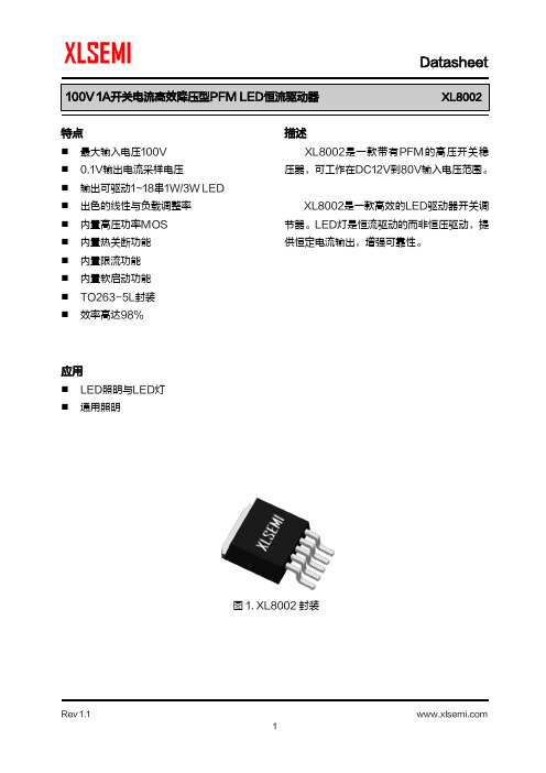
100V 1A 开关电流高效降压型PFM LED恒流驱动器XL8002特点⏹最大输入电压100V⏹0.1V输出电流采样电压⏹输出可驱动1~18串1W/3W LED ⏹出色的线性与负载调整率⏹内置高压功率MOS⏹内置热关断功能⏹内置限流功能⏹内置软启动功能⏹TO263-5L封装⏹效率高达98%应用⏹LED照明与LED灯⏹通用照明描述XL8002是一款带有PFM的高压开关稳压器,可工作在DC12V到80V输入电压范围。
XL8002是一款高效的LED驱动器开关调节器。
LED灯是恒流驱动的而非恒压驱动,提供恒定电流输出,增强可靠性。
图1. XL8002封装100V 1A 开关电流高效降压型PFM LED 恒流驱动器 XL8002引脚配置CSP VIN VREG STARTCSN 12345TO263-5L图2. XL8002引脚配置表1.引脚说明引脚号 引脚名 描述1 START 内部软启动引脚。
2 VREG 内部电压调节引脚。
(VREG 约为8V )3 VIN 电源输入引脚。
4 CSN 电流检测负端引脚。
5CSP电流检测正端引脚。
(电流检测基准电压为0.1V )100V 1A 开关电流高效降压型PFM LED 恒流驱动器 XL8002方框图EAHigh Voltage RegulatorReference VoltageVINCSN3.3V 0.1VEA COMP STARTCSPDMOSLatch and DricerThermal Shutdown0.12VOCP+- PFMFrequencyCompensationSoft-StartVREG 8V图3. XL8002方框图典型应用XL8002CIN 100uF/100VR1500KRCS 0.3ΩL1D1SS310LEDQ12N5551COUT 100uF/100VC22.2uFVINSTRAT VREG CSP CSN12345R23KC1105C3105ILED=0.1V/RCS Output 1~18 LED seriesVIN图4. XL8002系统参数测量电路100V 1A开关电流高效降压型PFM LED恒流驱动器XL8002图5. N*1W LED 效率曲线图6. N*1W LED负载调整率曲线100V 1A开关电流高效降压型PFM LED恒流驱动器XL8002订购信息产品型号打印名称封装方式包装类型XL8002E1 XL8002E1 TO263-5L 800只每卷XLSEMI无铅产品,产品型号带有“E1”后缀的符合RoHS标准。
技能培训常用模拟器件介绍

技能培训常用模拟器件介绍
MOS管全桥驱动电路
技能培训常用模拟器件介绍
光耦
光耦合器一般由三部分组成:光的发射、光的接 收及信号放大。输入的电信号驱动发光二极管 (LED),使之发出一定波长的光,被光探测器 接收而产生光电流,再经过进一步放大后输出。 这就完成了电—光—电的转换,从而起到输入、 输出、隔离的作用。由于光耦合器输入输出间互 相隔离,电信号传输具有单向性等特点,因而具 有良好的电绝缘能力和抗干扰能力。又由于光耦 合器的输入端属于电流型工作的低阻元件,因而 具有很强的共模抑制能力。所以,它在长线传输 信息中作为终端隔离元件可以大技能大培训常提用模高拟器件信介绍噪比。
• 可以用于升压、降压,小功率场合。包括电路里 的高转低等
• 基准为1.25V • 设计输出电压时, • 5脚按1.25V计算 • DIP8封装
技能培训常用模拟器件介绍
MC34063应用
技能培训常用模拟器件介绍
运放类
• 1、NE5534(双好) • 2、NE5532(双好) • 3、LM358(双) • 4、LM353(双) • 5、UA741(普通单) • 6、TL082(TL084)(双、四高阻) • 7、LM324(最常用四运放) • 8、仪表放大器
技能培训常用模拟器件介绍
常用三极管
• S9012 通用三极管 PNP,0.5A,25V,0.625W,150MHz,β=64~300 S9013 通用三极管 NPN,0.5A,25V,0.625W,150MHz,β=64~300 S9014 通用三极管 NPN,0.1A,45V,0.4W,150MHz,β=60~1000 S9015 通用三极管 PNP,0.1A,45V,0.4W,150MHz,β=60~1000 C1815 通用三极管 NPN,0.15A,50V,0.4W,80MHz,β=70~700 C945 通用三极管 NPN,0.15A,50V,0.4W,200MHz,β=70~700 S8550 通用三极管 PNP,0.5A,25V,0.625W,150MHz,β=85~300 S8050 通用三极管 NPN,0.5A,25V,0.625W,150MHz,β=85~300 2N5401 通用三极管 PNP,0.6A,150V,100MHz,β=80~250 2N5551 通用三极管 NPN,0.3A,160V,300MHz,β=80~250 D882 通用三极管 NPN,3A,30V,90MHz,β=60~400 IRF840 通用场效应管 N沟道增强型,8A,550V,125W,0.85Ω,TO-220封装 IRFP440 通用场效应管 N沟道增强型,8A,550V,125W,0.85Ω,TO-3P封装 37 IRF9642 通用场效应管 P沟道增强型,9A,200V,125W,0.7Ω,TO-220封装 IRFP9242 通用场效应管 P沟道增强型,9A,200V,125W,0.7Ω,,TO-3P封装
输入电压达40V以上的降压稳压系统的设计问题及其解决办法

输入电压达40V以上的降压稳压系统的设计问题及其解决办
法
Robert Bell
【期刊名称】《电子设计应用》
【年(卷),期】2007(0)3
【摘要】一般来说,我们会采用开关稳压器将不稳定的高输入电压降低为稳定的低输出电压。
对于必须通过直流/直流转换降低输入电压的系统来说,采用开关稳压器可大幅提高转换效率,这方面远比线性稳压器优胜。
大部分内置变压器的直流/直流转换器都采用回扫及正向的电路布局。
由于这两种布局的变压器匝数比可以按照不同要求加以设定,因此可以满足大部分降压转换的要求,
【总页数】4页(PI0001-I0001)
【关键词】输入电压;降压稳压系统;设计问题;直流/直流转换器;开关稳压器;线性稳压器;输出电压
【作者】Robert Bell
【作者单位】美国国家半导体应用技术工程师
【正文语种】中文
【中图分类】TM42
【相关文献】
1.宽输入电压降压稳压电路的设计与实现 [J], 刘炜航
2.专为高电压系统而设计美国国家半导体推出100V高集成度降压偏置稳压器 [J],
3.专为高电压系统而设计美国国家半导体推出100 V高集成度降压偏置稳压器/飞兆半导体全新VRM10.x兼容控制器/驱动器芯片组满足下一代VRM CPU和处理器的功率要求/安捷伦科技为手机和PDA推出业内最小的表面封装ChipLED [J],
4.输出电压达40V的宽输入电压范围升压稳压器 [J],
5.输入电压达40V以上的降压稳压系统的设计问题及其解决办法 [J], Robert Bell 因版权原因,仅展示原文概要,查看原文内容请购买。
- 1、下载文档前请自行甄别文档内容的完整性,平台不提供额外的编辑、内容补充、找答案等附加服务。
- 2、"仅部分预览"的文档,不可在线预览部分如存在完整性等问题,可反馈申请退款(可完整预览的文档不适用该条件!)。
- 3、如文档侵犯您的权益,请联系客服反馈,我们会尽快为您处理(人工客服工作时间:9:00-18:30)。
Features- 8V to 40V Input Voltage Range - Adjustable Output from 1.22V to 24V - Continuous 3A Output Current - Integrated 100mΩ MOSFET Switch- 1.22V Voltage Reference with ±2% Accuracy - Low 35µA Shutdown Current- Fixed 1.2x Output Over Voltage Protection - Fixed 150kHz Switching Frequency -Programmable CV/CC mode-Rapid Response Current Mode Operation- Over Voltage and Current Limit - Over Temperature Protection- RoHS 2.0 compliant SO-8P Green Package with Exposed PadGeneral DescriptionThe VP2140 is an efficiency and low-cost buck converter with integrated low R DS(ON) high-side 100mΩ MOSFET switch. It is capable of delivering 3A continuous output current with programmable current limit over a wide range of supplying voltage from 8V to 40V. With a simple voltage divider, the output voltage is easily adjustable from 1.22V to 24V.Other features such as 150kHz PWM frequency, output over-voltage protection, total fault-free protection and low 35µA shutdown current/ 1.2mA quiescent current make VP2140 ideally to be used in application like automotive equipments and networking devices.The VP2140 is available in popular SO-8P green package with exposed pad.Applications- Car Charger- Wireless Communication Device- Networking Device -LCD Monitor/ LCD TVTypical Application3A/40V/150kHz Buck Converter with CC modeFunctional Block DiagramPin Assignments And DescriptionsAbsolutely Maximum RatingsOver operating free-air temperature range, unless otherwise specified (* 1)( *1): Stress beyond those listed at “absolute maximum rating” table may cause permanent damage to the device. These are stress rating ONLY. For functional operation are strongly recommend follow up “recommended operation conditions” table.Recommended Operating ConditionsT A = 25℃, V IN = 24V, unless otherwise notedFunctional DescriptionsThe VP2140 is a fixed frequency, current mode asynchronous buck converter. During normal op-eration, the internal MOSFET switch is controlledby the gate driver and dominates the duty cycle of the PWM waveform. While the switch is turned off, the inductor current flows through the external diode.PWM OscillationThe frequency of the internal oscillator is fixed at 150kHz. In case of short circuit (output/feedback voltage is zero), the frequency will be down to 85kHz to reduce the heat and minimize the power consumption.Error AmplifierThe error amplifier compares the voltage of FB pin with the internal voltage reference V REF . When the output current increases, the voltage of FB pin de-creases and the error amplifier output will start to increase. This will force the gate driver to increase the duty cycle of the PWM waveform and raise the inductor current to compensate the output voltage drop.Adjusting Peak Switching CurrentTo adjust the peak switching current is easy by connecting a resistor R ISET from ISET pin to GND.Chip EnableThe VP2140 has an EN pin to perform chip enable control. The regulator can be enabled and disabled by simply applying state logic values on EN pin. The precision values of the rising threshold is 1V and the falling threshold is 0.8V. Never leave the EN pin floating and make sure the value of the logic away from the voltage region of risingthreshold and falling threshold.Under-voltage LockoutUnder-voltage lockout (UVLO) is implemented to protect the internal gate driver away from uncer-tain state and lose the control of the MOSFET switch. UVLO threshold voltage is 6.5V typically.Thermal ProtectionThermal shutdown is implemented to prevent the chip from operating at exceedingly high temperatures. When the silicon die temperature is higher than its upper threshold, it forces the whole chip entering shutdown state. When the temperature is lower than its lower threshold, it resumes the normal operation.Output VoltageIn Figure 1, the output voltage can be set by the resistor network connected to the output voltage terminal and FB pin. The resistor network divides the output voltage down to the feedback voltage by the follow ratio:where V FB is the feedback voltage, V OUT is the out-put voltage.Thus the output voltage can be obtained by the following equation:212OUTFB R R R V V +=1(21R R V V FB OUT +×=Functional Descriptions (cont.)Figure 1. Output network of VP2140Application InformationThe VP2140 is an asynchronous high voltage buck converter that can support the input voltage range from 7V to 40V and the output current can be up to 3A.Inductor SelectionThe value of the inductor affects the ripples of output voltage and must be carefully selected. In the same working condition, larger inductance value results in lower output ripple voltage but such inductor will be oversized, higher series re-sistance and lower saturation current.In most cases, it would be a good rule to keep peak-to-peak switching current ∆I L to be approxi-mate 30% of the maximum switching current. And it is necessary to assure the peak inductor current is under maximum switch current limit. Thus, the inductance can be calculated by the following equation:where f is the switch frequency, L is the induc-tance.Hence the maximum peak current limit of the in-ductor I L(PEAK) can be obtained by:where I LOAD is the maximum load current.With the equations listed above, the inductance of inductor can be calculated easily. Actually, the se-lection of the inductor is the compromise of the cost, size, electrical specification and desired elec-tro-magnetic compatibility.Output Rectifier Diode)(INOUTL OUT V V 1I f V L −∆×=()(INOUTOUT L LOAD PEAK L V V 1L f 2V I I I −×=∆+=The output rectifier diode supplies the current to the inductor when the high-side switch is off. To reduce losses due to the diode forward voltage and recovery times, it is recommended to use a Schottky diode. Choose a diode whose maxi-mum reverse voltage rating is greater than the maximum input voltage, and whose currentrating is greater than the maximum load current. Input Capacitor SelectionThe VP2140 requires an input decoupling capaci-tor and a bulk capacitor is needed depending on the application. The use of low ESR capacitors can give the benefits of better performance and less ripple voltage.The input capacitor should be considered with the RMS current rating. The following equation shows how t could be estimated:where Duty is the PWM duty cycle, ILOAD(MAX) is the maximum load current.Therefore, select input capacitor with ripple cur-rent rating larger than half of the maximum load current.The input ripple voltage ∆VIN depends on the ESR and capacitance of input capacitor. The value ofthe input capacitor can be determined as the fol-lowings:Input capacitor could cause significant conduction loss if the input current is large enough. Its power dissipation is listed below:)1()()(Duty Duty I I MAX LOAD CIN RMS −××=)()1()()(ESR I V f Duty Duty I C MAX LOAD IN MAX LOAD IN ×−∆×−××=Application Information (cont.)When selecting input capacitor, make sure the ca-pacitance is enough to prevent the excessive input ripple current. If using aluminum electrolytic input capacitors, parallel connecting 0.1µF speed-up capacitor as close to the regulator as possible.Output Capacitor SelectionThe output capacitor is to maintain output voltage and reduce output ripple voltage ∆V OUT and the low ESR capacitor is preferred. The output ripple volt-age can be obtained by the following equation:Boot-Strap Capacitor SelectionA 100nF ceramic capacitor must be connected be-tween the BS pin to LX pin for proper operation. It is recommended to use a ceramic capacitor.ESRI P CIN RMS CIN D ×=2)()()81(OUTL OUT C f ESR I V ××+×∆=∆Application Information (cont.)Package Information SO-8PThermal Enhanced DimensionsNotes:1. Package Outline Unit Description:BSC: Basic. Represents theoretical exact dimension or dimension target. MIN: Minimum dimension specified. MAX: Maximum dimension specified.REF: Reference. Represents dimension for reference use only. This value is not a device specification. TYP: Typical. Provided as a general value. This value is not a device specification. 2. Dimensions in Millimeters.3. JEDEC Outline : MS-012 AA Rev. F (Standard), MS-012 BA Rev. F (Thermal)4. Dimensions “D” does not include mold flash, protrusions or gate burrs. Mold flash, protrusions and gate burrs shall not exceed 0.51mm per side.5. Dimensions “E1” does not include inter-lead flash, or protrusions. Inter-lead flash and protrusions shall not exceed 0.25mm per side.VP2140Preliminary Contact Information Viva Electronics Incorporated10F-1, No. 32, Gaotie 2nd Rd., Zhubei City, Hsinchu County, Taiwan, R.O.C. Tel: 886-3-6579508Fax: 886-3-6579509WWW: Sales: sales@FAE Support: fae@IMPORTANT NOTICEViva Electronics Incorporated reserves the right to make changes without further notice to any products or specifications herein. Viva Electronics Incorporated does not assume any responsibility for use of any its products for any particular purpose, nor does Viva Electronics Incorporated assume any liability arising out of the application or use of any its products or circuits. Viva Elec-。