442005[高电压技术]
4425中文
ML4425脉宽调制无刷电机控制器特征:1)可独立工作;2)通过IC控制电机的起动和停止;3)机载起动时序为校准→斜升→设定速度;4)获专利的反电势换向技术为最短的“自转”时间提供了无抖动转矩;5)具有机载速度控制环;6)用于换向的锁相环PLL可对PWM产生的尖峰脉冲噪声的抗干扰创造条件,其作用与噪声传感过零技术相似;7)PWM控制可得到最高效率;8)MOSFET直接驱动12V电机;驱动高压电机需要用IR、IXYS、Harris、PowerIntegration、Siliconix等公司生产的IC缓冲器。
1引言ML4425脉宽调制控制器具有为起动和控制△接或Y接无刷直流(BLDC)电机速度所需要的全部功能,并且不用霍尔传感器。
从电机绕组传感的反电势电压信号,利用锁相环(PLL)即可确定正确的换向时序,这一获专利的传感技术可以在宽范围内使三相无刷电机换向,并且对PWM噪声和电机缓冲电路的干扰不敏感。
ML4425利用恒定的关断时间PWM控制环路,限制电机的工作电流。
其速度环是由片内放大器控制。
ML4425电路能保证没有穿透(shoot-through in)而直接驱动外部功率MOSFET。
起动程序的定时由三个可供选择的定时电容器来确定。
这就使大范围变化的电机和负载能够处于最佳状态。
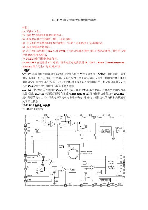
2 ML4425的结构与参数2.1ML4425的结构脚1:ISENSE:电机的电流传感输入端。
当ISENSE超过0.2³ILIMIT时,三路输出驱动器LA、LB、LC一个固定时间均被关闭在(由CIOS电容量确定)。
脚2:A相上桥开关的低输出驱动器。
脚3:B相上桥开关的低输出驱动器。
脚4:C相上桥开关的低输出驱动器。
脚5:SPEEDCOMP:是速度控制环的补偿端,它由接在SPEEDCOMP脚与地端之间的串联的电阻器和电容器来设置。
脚6:CT:一只电容器接CT与地之间,可设定PWM振荡器频率。
脚7:VREF:6.9V基准参考电压输出。
发电机组控制器4420

PLANT +VE
4 FET OUTPUTS
MBCR
*
17 18 19 20
USB PROGRAMMING PORT
ENGINE ECU
H L
21 22 23 24 25 26
67 8 9
14 12 13
FUEL
CONNECT THE SCREEN TO
ENGINE ONLY
TESTING STANDARDS
Both modules include six digital inputs and six outputs. Four outputs are configurable on the magnetic pick-up version and six are configurable on the Canbus version. The modules can either be programmed using the front panel or by using the DSE Configuration Suite PC software.
BENEFITS • Transfers between mains (utility)
and generator power (DSE4420 only) • Hours counter provides accurate information for monitoring and maintenance periods • User-friendly set-up and button layout. Multiple engine parameters are monitored simultaneously • Module can be configured to suit individual applications. Wide range of engines can be specified IP65/NEMA 12 rating offers advanced resistance to water ingress • License free PC software
高电压测试技术
高电压测试技术-高电压测试技术高电压测试技术-正文研究各种高电压和大电流的产生、测量、试验及应用的一门工程技术。
是高电压技术的重要组成部分。
高电压测试技术主要用于电力设备绝缘试验、开关设备断流试验、电力系统过电压测试以及各种类型放电现象的试验研究等。
除传统的应用领域外,它还广泛应用于机加工、纺织、印刷、除尘、勘探、医疗等各种行业,并已成为激光、高能粒子、热核聚变等高技术领域中不可缺少的一种技术手段。
高电压试验和应用的种类很多,需要应用各种不同的稳态或暂态的高电压和大电流。
常用的稳态高电压有工频交流电压和直流电压,用作试验电压或工作电压。
常用的暂态高电压和大电流有冲击电压和冲击电流以及工频振荡电流等。
前者模拟雷电过电压或操作过电压,后两者分别模拟雷电流及短路电流。
此外,还有一些特殊的方波电压、方波电流、强流脉冲以及纳秒级的核致电磁脉冲(NEMP)等。
高电压发生装置产生上述高电压和大电流的设备通常采用交流高压试验变压器、直流高压发生器、冲击电压发生器、冲击电流发生器、合成振荡回路等。
这些设备都是以试验变压器和高压电容器为主体,以不同接线所构成。
试验变压器可产生工频交流高电压,也可用作其他设备的交流高压电源。
高压电容器与硅堆等组成的各种整流回路,可产生直流高电压,也可用作其他设备的直流高压电源。
多台高压电容器并联充电、串联放电的Marx回路可产生很高的冲击电压。
多台高压电容器并联,通过低阻抗放电可产生很大的冲击电流;若通过电感线圈放电,则可产生衰减振荡的电流或电压,并可用以构成振荡回路等。
除上述常规设备外,还可由这些设备改装或组合,用以产生陡波冲击电压、交流叠加冲击波电压等;也可利用高压电容器等基本部件构成各种各样的特殊设备,例如电容电感链型回路或同轴型形成线,它们都可产生很高的方波电压或很大的方波电流等。
高电压测试技术测量仪器测量各种高电压和大电流的装置通常采用测量球隙、静电电压表(见图)、分压器、分流器、电压互感器、电流互感器等。
一种基于KNbO-Au NPs@BiS构建的电化学发光免疫传感器的制备方法及应用
专利名称:一种基于KNbO-Au NPs@BiS构建的电化学发光免疫传感器的制备方法及应用
专利类型:发明专利
发明人:马洪敏,魏琴,王晓东,庞雪辉,李建修,杜斌,范大伟,曹伟,胡丽华,吴丹,张勇,李贺
申请号:CN201510262842.9
申请日:20150522
公开号:CN104849458A
公开日:
20150819
专利内容由知识产权出版社提供
摘要:本发明属于纳米功能材料,免疫分析以及生物传感技术领域,提供了一种铌酸钾负载金的硫化铋构建的电化学发光免疫传感器的制备方法及其应用。
采用铌酸钾负载金作为基底材料,硫化铋作为发光材料的电化学发光免疫传感器。
对肿瘤的早期诊断以及临床应用方面具有重要的实用性。
申请人:济南大学
地址:250022 山东省济南市济微路106号
国籍:CN
更多信息请下载全文后查看。
电工技师论文74205-范本模板
青岛市维修电工技师论文题目:基于欧姆龙PLC的变频器恒压供水姓名:单位:指导老师:日期:摘要随着经济的飞速发展,人们对供水质量和供水系统可靠性的要求不断提高,再加上目前能源紧缺。
本论文结合我国水资源与电能资源短缺和中小城市供水厂的现状,设计了一套基于PLC的变频恒压供水控制系统。
变频恒压供水控制系统由可编程控制器、变频器、水泵电机组、压力传感器等构成。
本系统采用了PLC的控制方式,完成了系统数据采集和通信、水泵机组的变频控制、系统监控管理等功能模块的设计,实现了变频恒压供水自动控制。
系统采用一台变频器控制四台电动机的控制方式,四台电动机采用循环运行的方式。
本文基于德国SIMENS公司的S7-200 PLC完成了恒压供水控制系统PID控制器的设计.PID控制器根据压力给定值与测量值的偏差,实时控制变频器的输出电压和频率,进而改变水泵电动机的转速来改变水泵出水口流量,实现管网压力的自动调节,使管网压力稳定在设定值附近.现场调试和运行结果表明,该系统能够对供水过程实现自动控制,控制效果良好,并能够有效地降低能耗,达到了节水节电的目的,同时能够保证供水系统维持在最佳状况,提高了生产管理水平,实现了节能能耗的目标。
关键词:恒压供水系统,可编程序控制器,变频调速,PID目录第一章绪论 (1)1.1选题的背景及意义 (1)1.2 变频恒压供水系统的国内外研究现状 (1)1.3 变频恒压供水系统原理概述 (2)1.4 本文研究的内容 (3)第二章变频恒压供水系统理论分析和方案论证 (4)2。
1 变频恒压供水系统理论分析 (4)2。
1。
1 变频恒压供水系统节能原理 (4)2.1。
2 变频恒压控制系统的数学模型及分析 (6)2.2 变频恒压供水系统控制流程 (7)2。
2.1 水泵机组变频恒压流程 (7)2.2.2 供水系统中水泵切换条件分析 (11)2。
3 变频恒压供水系统控制系统组成 (14)第三章硬件系统设计 (15)3。
3-1电介质极化
相对介电常数: 相对介电常数:
高电压技术精品课程
电介质极化在工程上的意义: 电介质极化在工程上的意义:
1、选择电介质时,应注意相对介电常数 、选择电介质时, 用作电容器的绝缘介质时 用作电容器的绝缘介质时,希望
大些好。 ε r 大些好。 用作其它设备的绝缘介质时 小些好。 用作其它设备的绝缘介质时,希望 ε r 小些好。 2、 几种绝缘介质组合在一起使用时,应注意 ε r 的配合。 的配合。 、 几种绝缘介质组合在一起使用时, 3、 材料的介质损耗与极化形式有关,而介质损耗是 、 材料的介质损耗与极化形式有关, 影响绝缘劣化和热击穿的一个重要因素。 影响绝缘劣化和热击穿的一个重要因素。 4、 在绝缘预防性试验中,夹层极化现象可用来判断 、 在绝缘预防性试验中, 绝缘受潮情况。 绝缘受潮情况。
εr
的大小。 的大小。
高电压技术精品课程
电子式极化
电子式极化特点:时间短,无能量损耗, 电子式极化特点:时间短,无能量损耗,弹性极化
高电压技术精品课程
离子式极化
离子式极化特点:时间短,无能量损耗, 离子式极化特点:时间短,无能量损耗,弹性极化
高电压技术精品课程
第三章 液体和固体电介质的 电气特性
《高电压技术》课题组 高电压技术》
高电压技术精品课程
3-1 电介质的极化
目的 1.熟悉电介质在电场作用下的极化现象 1.熟悉电介质在电场作用下的极化现象 2.了解电介质极化在工程上的合理应用 2.了解电介质极化在工程上的合理应用 方法 1、 案例分析、讲解演示 案例分析、 讨论交流、 2、 讨论交流、归纳总结
高电压技术精品课程
偶子式极化
偶极子式极化特点:时间较长,有能量损耗, 偶极子式极化特点:时间较长,有能量损耗,非弹性极化高ຫໍສະໝຸດ 压技术精品课程 夹层式极化
PCS-9621N_X_说明书_国内中文准版
我们对本文档及其中的内容具有全部的知识产权。除非特别授权,禁 止复制或向第三方分发。凡侵犯本公司版权等知识产权的,本公司必 依法追究其法律责任。
购买产品,请联系: 电话:025-87178911,传真: 025-52100511、025-52100512 电子信箱:market@
本手册中将会用到以下指示标记和标准定义:
危险! 意味着如果安全预防措施被忽视,则会导致人员死亡,严重的人身伤害,或 严重的设备损坏。
警告! 意味着如果安全预防措施被忽视,则可能导致人员死亡,严重的人身伤害, 或严重的设备损坏。
警示! 意味着如果安全预防措施被忽视,则可能导致轻微的人身伤害或设备损坏。 本条特别适用于对装置的损坏及可能对被保护设备的损坏。
特别注意,一些通用的工作于高压带电设备的工作规则必须遵守。如果不遵守可能导致严重的 人身伤亡或设备损坏。
危险!
在一次系统带电运行时,绝对不允许将与装置连接的电流互感器二次开路。该回路开路可能会 产生极端危险的高压。
南京南瑞继保电气有限公司
i
PCS-9621N 站用变保护装置
警告!
z 曝露端子 在装置带电时不要触碰曝露的端子等,因为可能会产生危险的高电压。
1.1 应用范围 ...........................................................................................................................1 1.2 功能配置 ...........................................................................................................................1 1.3 性能特征 ...........................................................................................................................2 1.4 订货须知 ...........................................................................................................................3 第 2 章 技术参数 ............................................................................................................................4 2.1 电气参数 ...........................................................................................................................4 2.2 机械结构 ...........................................................................................................................5 2.3 环境条件参数 ....................................................................................................................6 2.4 通信端口 ...........................................................................................................................6 2.5 型式试验 ...........................................................................................................................7 2.6 认证 ..................................................................................................................................7 2.7 保护功能 ...........................................................................................................................8 2.8 管理功能 ...........................................................................................................................8 第 3 章 工作原理 ..........................................................................................................................10 3.1 概述 ................................................................................................................................10 3.2 装置启动元件 ..................................................................................................................10 3.3 过流保护 ......................................................................................................................... 11 3.4 高压侧接地保护 .............................................................................................................. 11 3.5 低压侧接地保护 .............................................................................................................. 11 3.6 非电量保护......................................................................................................................12 3.7 闭锁简易母线保护...........................................................................................................12 3.8 遥控、遥测、遥信功能....................................................................................................12 3.9 时间管理 .........................................................................................................................12 第 4 章 硬件描述 ..........................................................................................................................14 4.1 装置面板布置 ..................................................................................................................14
MIC4424中文资料
MIC4424中⽂资料MIC4423/4424/4425 Electrical Characteristics4.5V ≤ V S ≤ 18V; T A = 25°C, bold values indicate –40°C ≤ T A ≤ +85°C; unless noted.Symbol ParameterConditionsMinTypMaxUnitsInput V IH Logic 1 Input Voltage 2.4V V IL Logic 0 Input Voltage 0.8V I IN Input Current0V ≤ V IN ≤ V S–11µA –1010µAOutput V OH High Output Voltage V S –0.025V V OL Low Output Voltage 0.025V R OOutput Resistance HI StateI OUT = 10mA, V S = 18V2.85?V IN = 0.8V, I OUT = 10mA, V S = 18V3.78?Output Resistance LO StateI OUT = 10mA, V S = 18V3.55?V IN = 2.4V, I OUT = 10mA, V S = 18V4.38I PK Peak Output Current 3A ILatch-Up Protection>500mAWithstand Reverse CurrentSwitching Time (Note 4)t R Rise Time test Figure 1, C L = 1800pF 2335ns 2860ns t F Fall Time test Figure 1, C L = 1800pF 2535ns 3260ns t D1Delay Tlme test Ffigure 1, C L = 1800pF 3375ns 32100ns t D2Delay Timetest Figure 1, C L = 1800pF3875ns 38100nsPower Supply I S Power Supply Current V IN = 3.0V (both inputs) 1.5 2.5mA 2 3.5mA I SPower Supply CurrentV IN = 0.0V (both inputs)0.150.25mA 0.20.3mANote 1.Exceeding the absolute maximum rating may damage the device.Note 2.The device is not guaranteed to function outside its operating rating.Note 3.Devices are ESD sensitive. Handling precautions recommended. ESD tested to human body model, 1.5k in series with 100pF.Note 4.Switching times guaranteed by design.Absolute Maximum Ratings (Note 1)Supply Voltage (22)Input Voltage.................................V S + 0.3V to GND – 5V Junction Temperature ..............................................150°C Storage Temperature Range ....................–65°C to 150°C Lead Temperature (10 sec.).....................................300°C ESD Susceptability, Note 3.. (1000V)Operating Ratings (Note 2)Supply Voltage (V S )....................................+4.5V to +18V Temperature RangeC Version ..................................................0°C to +70°C B Version...............................................–40°C to +85°C Package Thermal ResistanceDIP θJA .............................................................130°C/W DIP θJC ...............................................................42°C/W Wide-SOIC θJA .................................................120°C/W Wide-SOIC θJC ...................................................75°C/W SOIC θJA ..........................................................120°C/W SOIC θJC ............................................................75°C/WApplication InformationAlthough the MIC4423/24/25 drivers have been specifically constructed to operate reliably under any practical circumstances, there are nonetheless details of usage which will provide better operation of the device.Supply BypassingCharging and discharging large capacitive loads quickly requires large currents. For example, charging 2000pF from 0 to 15 volts in 20ns requires a constant current of 1.5A. In practice, the charging current is not constant, and will usually peak at around 3A. In order to charge the capacitor, the driver must be capable of drawing this much current, this quickly, from the system power supply. In turn, this means that as far as the driver is concerned, the system power supply, as seen by the driver, must have a VERY low impedance.As a practical matter, this means that the power supply bus must be capacitively bypassed at the driver with at least 100X the load capacitance in order to achieve optimum driving speed. It also implies that the bypassing capacitor must have very low internal inductance and resistance at all frequencies of interest. Generally, this means using two capacitors, one a high-performance low ESR film, the other a low internal resistance ceramic, as together the valleys in their two impedance curves allow adequate performance over a broad enough band to get the job done. PLEASE NOTE that many film capacitors can be sufficiently inductive as to be useless for this service. Likewise, many multilayer ceramic capacitors have unacceptably highinternal resistance. Use capacitors intended for high pulse current service (in-house we use WIMA? film capacitors and AVX Ramguard? ceramics; several other manufacturers of equivalent devices also exist). The high pulse current demands of capacitive drivers also mean that the bypass capacitors must be mounted very close to the driver in order to prevent the effects of lead inductance or PCB land inductance from nullifying what you are trying to accomplish. For optimum results the sum of the lengths of the leads and the lands from the capacitor body to the driver body should total 2.5cm or less.Bypass capacitance, and its close mounting to the driver serves two purposes. Not only does it allow optimum performance from the driver, it minimizes the amount of lead length radiating at high frequency during switching, (due to the large ? I) thus minimizing the amount of EMI later available for system disruption and subsequent cleanup. It should also be noted that the actual frequency of the EMI produced by a driver is not the clock frequency at which it is driven, but is related to the highest rate of change of current produced during switching, a frequency generally one or two orders of magnitude higher, and thus more difficult to filter if you let it permeate your system. Good bypassing practice is essential to proper operation of high speed driver ICs. GroundingBoth proper bypassing and proper grounding are necessary for optimum driver operation. Bypassing capacitance only allows a driver to turn the load ON. Eventually (except in rare circumstances) it is also necessary to turn the load OFF. This requires attention to the ground path. Two things other than the driver affect the rate at which it is possible to turn a load off: The adequacy of the grounding available for the driver, and the inductance of the leads from the driver to the load. The latter will be discussed in a separate section.Best practice for a ground path is obviously a well laid out ground plane. However, this is not always practical, and a poorly-laid out ground plane can be worse than none. Attention to the paths taken by return currents even in a ground plane is essential. In general, the leads from the driver to its load, the driver to the power supply, and the driver to whatever is driving it should all be as low in resistance and inductance as possible. Of the three paths, the ground lead from the driver to the logic driving it is most sensitive to resistance or inductance, and ground current from the load are what is most likely to cause disruption. Thus, these ground paths should be arranged so that they never share a land, or do so for as short a distance as is practical.To illustrate what can happen, consider the following: The inductance of a 2cm long land, 1.59mm (0.062") wide on a PCB with no ground plane is approximately 45nH. Assuming a dl/dt of 0.3A/ns (which will allow a current of 3A to flow after 10ns, and is thus slightly slow for our purposes) a voltage of 13.5 Volts will develop along this land in response to our postulated Ι. For a 1cm land, (approximately 15nH) 4.5 Volts is developed. Either way, anyone using TTL-level input signals to the driver will find that the response of their driver has been seriously degraded by a common ground path for input to and output from the driver of the given dimensions. Note that this is before accounting for any resistive drops in the circuit. The resistive drop in a 1.59mm (0.062") land of 2oz. Copper carrying 3A will be about 4mV/cm (10mV/in) at DC, and the resistance will increase with frequency as skin effect comes into play.The problem is most obvious in inverting drivers where the input and output currents are in phase so that any attempt to raise the driver’s input voltage (in order to turn the driver’s load off) is countered by the voltage developed on the common ground path as the driver attempts to do what it was supposed to. It takes very little common ground path, under these circumstances, to alter circuit operation drastically.Output Lead InductanceThe same descriptions just given for PCB land inductance apply equally well for the output leads from a driver to its load, except that commonly the load is located much further away from the driver than the driver’s ground bus.Generally, the best way to treat the output lead inductance problem, when distances greater than 4cm (2") are involved, requires treating the output leads as a transmission line. Unfortunately, as both the output impedance of the driver and the input impedance of the MOSFET gate are at least an order of magnitude lower than the impedance of common coax, using coax is seldom a cost-effective solution. A twisted pair works about as well, is generally lower in cost, and allows use of a wider variety of connectors. The second wire of the twisted pair should carry common from as close as possibleto the ground pin of the driver directly to the ground terminal of the load. Do not use a twisted pair where the second wire in the pair is the output of the other driver, as this will not provide a complete current path for either driver. Likewise, do not use a twisted triad with two outputs and a common return unless both of the loads to be driver are mounted extremely close to each other, and you can guarantee that they will never be switching at the same time.For output leads on a printed circuit, the general rule is to make them as short and as wide as possible. The lands should also be treated as transmission lines: i.e. minimize sharp bends, or narrowings in the land, as these will cause ringing. For a rough estimate, on a 1.59mm (0.062") thick G-10 PCB a pair of opposing lands each 2.36mm (0.093") wide translates to a characteristic impedance of about 50?. Half that width suffices on a 0.787mm (0.031") thick board. For accurate impedance matching with a MIC4423/24/25 driver, on a 1.59mm (0.062") board a land width of 42.75mm (1.683") would be required, due to the low impedance of the driver and (usually) its load. This is obviously impractical under most circumstances. Generallythe tradeoff point between lands and wires comes when lands narrower than 3.18mm (0.125") would be required on a1.59mm (0.062") board.To obtain minimum delay between the driver and the load, it is considered best to locate the driver as close as possible to the load (using adequate bypassing). Using matching transformers at both ends of a piece of coax, or several matched lengths of coax between the driver and the load, works in theory, but is not optimum.Driving at Controlled RatesOccasionally there are situations where a controlled rise or fall time (which may be considerably longer than the normal rise or fall time of the driver’s output) is desired for a load. In such cases it is still prudent to employ best possible practice in terms of bypassing, grounding and PCB layout, and then reduce the switching speed of the load (NOT the driver) by adding a noninductive series resistor of appropriate value between the output of the driver and the load. For situations where only rise or only fall should be slowed, the resistor can be paralleled with a fast diode so that switching in the other direction remains fast. Due to the Schmitt-trigger action of the driver’s input it is not possible to slow the rate of rise (or fall) of the driver’s input signal to achieve slowing of the output. Input StageThe input stage of the MIC4423/24/25 consists of a single-MOSFET class A stage with an input capacitance of ≤38pF. This capacitance represents the maximum load from the driver that will be seen by its controlling logic. The drain load on the input MOSFET is a –2mA current source. Thus, the quiescent current drawn by the driver varies, depending on the logic state of the input.Following the input stage is a buffer stage which provides ~400mV of hysteresis for the input, to prevent oscillations when slowly-changing input signals are used or when noise is present on the input. Input voltage switching threshold is approximately 1.5V which makes the driver directly compatible with TTL signals, or with CMOS powered from any supply voltage between 3V and 15V.The MIC4423/24/25 drivers can also be driven directly by the SG1524/25/26/27, TL494/95, TL594/95, NE5560/61/62/68, TSC170, MIC38C42, and similar switch mode power supply ICs. By relocating the main switch drive function into the driver rather than using the somewhat limited drive capabilities of a PWM IC. The PWM IC runs cooler, which generally improves its performance and longevity, and the main switches switch faster, which reduces switching losses and increase system efficiency.The input protection circuitry of the MIC4423/24/25, in addition to providing 2kV or more of ESD protection, also works to prevent latchup or logic upset due to ringing or voltage spiking on the logic input terminal. In most CMOS devices when the logic input rises above the power supply terminal, or descends below the ground terminal, the device can be destroyed or rendered inoperable until the power supply is cycled OFF and ON. The MIC4423/24/25 drivers have been designed to prevent this. Input voltages excursions as great as 5V below ground will not alter the operation of the device. Input excursions above the power supply voltage will result in the excess voltage being conducted to the power supply terminal of the IC. Because the excess voltage is simply conducted to the power terminal, if the input to the driver is left in a high state when the power supply to the driver is turned off, currents as high as 30mA can be conducted through the driver from the input terminal to its power supply terminal. This may overload the output of whatever is driving the driver, and may cause other devices that share the driver’s power supply, as well as the driver, to operate when they are assumed to be off, but it will not harm the driver itself. Excessive input voltage will also slow the driver down, and result in much longer internal propagation delays within the drivers. T D2, for example, may increase to several hundred nanoseconds. In general, while the driver will accept this sort of misuse without damage, proper termination of the line feeding the driver so that line spiking and ringing are minimized, will always result in faster and more reliable operation of the device, leave less EMI to be filtered elsewhere, be less stressful to other components in the circuit, and leave less chance of unintended modes of operation. Power DissipationCMOS circuits usually permit the user to ignore power dissipation. Logic families such as 4000 series and 74Cxxx have outputs which can only source or sink a few milliamps of current, and even shorting the output of the device to ground or V CC may not damage the device. CMOS drivers, on the other hand, are intended to source or sink several Amps of current. This is necessary in order to drive large capacitive loads at frequencies into the megahertz range. Package power dissipation of driver ICs can easily be exceeded when driving large loads at high frequencies. Care must therefore be paid to device dissipation when operating in this domain. The Supply Current vs Frequency and Supply Current vs Load characteristic curves furnished with this data sheet aidin estimating power dissipation in the driver. Operating frequency, power supply voltage, and load all affect power dissipation.Given the power dissipation in the device, and the thermal resistance of the package, junction operating temperature for any ambient is easy to calculate. For example, the thermal resistance of the 8-pin plastic DIP package, from the datasheet, is150°C/W. In a 25°C ambient, then, using a maximum junction temperature of 150°C, this package will dissipate 960mW. Accurate power dissipation numbers can be obtained by summing the three sources of power dissipation in the device:? Load power dissipation (P L)Quiescent power dissipation (P Q)Transition power dissipation (P T)Calculation of load power dissipation differs depending on whether the load is capacitive, resistive or inductive. Resistive Load Power DissipationDissipation caused by a resistive load can be calculated as: P L = I2 R O Dwhere:I =the current drawn by the loadR O =the output resistance of the driver when theoutput is high, at the power supply voltage used(See characteristic curves)D =fraction of time the load is conducting (duty cycle) Capacitive Load Power DissipationDissipation caused by a capacitive load is simply the energy placed in, or removed from, the load capacitance by the driver. The energy stored in a capacitor is described by the equation:E = 1/2 C V2As this energy is lost in the driver each time the load is charged or discharged, for power dissipation calculations the 1/2 is removed. This equation also shows that it is good practice not to place more voltage in the capacitor than is necessary, as dissipation increases as the square of the voltage applied to the capacitor. For a driver with a capacitive load:P L = f C (V S)2where:f =Operating FrequencyC =Load CapacitanceV S =Driver Supply VoltageInductive Load Power DissipationFor inductive loads the situation is more complicated. For the part of the cycle in which the driver is actively forcing current into the inductor, the situation is the same as it is in the resistive case:P L1 = I2 R O DHowever, in this instance the R O required may be either the on resistance of the driver when its output is in the high state, or its on resistance when the driver is in the low state, depending on how the inductor is connected, and this is still only half the story. For the part of the cycle when the inductor is forcing current through the driver, dissipation is best described asP L2 = I V D (1 – D)where V D is the forward drop of the clamp diode in the driver (generally around 0.7V). The two parts of the load dissipation must be summed in to produce P LP L = P L1 + P L2Quiescent Power DissipationQuiescent power dissipation (P Q, as described in the input section) depends on whether the input is high or low. A low input will result in a maximum current drain (per driver) of ≤0.2mA; a logic high will result in a current drain of ≤2.0mA. Quiescentpower can therefore be found from:P Q = V S [D I H + (1 – D) I L]where:I H =quiescent current with input highI L =quiescent current with input lowD = fraction of time input is high (duty cycle)V S =power supply voltageTransition Power DissipationTransition power is dissipated in the driver each time its output changes state, because during the transition, for a very brief interval, both the N- and P-channel MOSFETs in the output totem-pole are ON simultaneously, and a current is conducted through them from V S to ground. The transition power dissipation is approximately:P T = f V S (A?s)where (A?s) is a time-current factor derived from Figure 2.Total power (P D) then, as previously described is justP D = P L + P Q +P TExamples show the relative magnitude for each term.EXAMPLE 1: A MIC4423 operating on a 12V supply driving two capacitive loads of 3000pF each, operating at 250kHz, with a duty cycle of 50%, in a maximum ambient of 60°C.First calculate load power loss:P L = f x C x (V S)2P L= 250,000 x (3 x 10–9 + 3 x 10–9) x 122= 0.2160WThen transition power loss:P T = f x V S x (A?s)= 250,000 ? 12 ? 2.2 x 10–9 = 6.6mWThen quiescent power loss:P Q= V S x [D x I H + (1 – D) x I L]= 12 x [(0.5 x 0.0035) + (0.5 x 0.0003)]= 0.0228WTotal power dissipation, then, is:P D= 0.2160 + 0.0066 + 0.0228= 0.2454WAssuming an SOIC package, with an θJA of 120°C/W, this will result in the junction running at:0.2454 x 120 = 29.4°Cabove ambient, which, given a maximum ambient temperature of 60°C, will result in a maximum junction temperature of 89.4°C.EXAMPLE 2: A MIC4424 operating on a 15V input, with one driver driving a 50? resistive load at 1MHz, with a duty cycle of67%, and the other driver quiescent, in a maximum ambient temperature of 40°C:P L = I2 x R O x DFirst, I O must be determined.I O = V S / (R O + R LOAD)Given R O from the characteristic curves then,I O = 15 / (3.3 + 50)I O = 0.281Aand:P L= (0.281)2 x 3.3 x 0.67= 0.174WP T= F x V S x (A?s)/2(because only one side is operating)= (1,000,000 x 15 x 3.3 x 10–9) / 2= 0.025 Wand:P Q = 15 x [(0.67 x 0.00125) + (0.33 x 0.000125) +(1 x 0.000125)](this assumes that the unused side of the driver has its input grounded, which is more efficient)= 0.015Wthen:P D= 0.174 + 0.025 + 0.0150= 0.213WIn a ceramic package with an θJA of 100°C/W, this amount of power results in a junction temperature given the maximum 40°C ambient of:(0.213 x 100) + 40 = 61.4°CThe actual junction temperature will be lower than calculated both because duty cycle is less than 100% and because the graph lists R DS(on) at a T J of 125°C and the R DS(on) at 61°C T J will be somewhat lower.DefinitionsC L =Load Capacitance in Farads.D =Duty Cycle expressed as the fraction of time the inputto the driver is high.f =Operating Frequency of the driver in HertzI H =Power supply current drawn by a driver when bothinputs are high and neither output is loaded.I L =Power supply current drawn by a driver when bothinputs are low and neither output is loaded.I D =Output current from a driver in Amps.P D =Total power dissipated in a driver in Watts.P L =Power dissipated in the driver due to the driver’s load in Watts.P Q =Power dissipated in a quiescent driver in Watts.P T=Power dissipated in a driver when the output changes states (“shoot-through current”) in Watts. NOTE: The “shoot-through” current from a dual transition (onceup, once down) for both drivers is stated in the graphon the following page in ampere-nanoseconds. Thisfigure must be multiplied by the number of repetitionsper second (frequency to find Watts).R O=Output resistance of a driver in Ohms.V S=Power supply voltage to the IC in Volts.。
绝缘油抗氧化剂的选择及其协同抗氧化作用_廖瑞金(1)
高电压技术 第38卷第1期2012年1月31日High Voltage Engineering,Vol.38,No.1,January 31,2012绝缘油抗氧化剂的选择及其协同抗氧化作用廖瑞金1,郝 建1,梁帅伟2,朱孟兆1,杨丽君1(1.重庆大学输配电装备及系统安全与新技术国家重点实验室,重庆400030;2.宁波电业局,宁波315010)摘 要:为了从根本上提高矿物油与天然酯混合绝缘油的氧化安定性,通过加压差示扫描量热法(PDSC)选取了适用于混合油的最佳抗氧化剂复配方式;对比了加入复合抗氧化剂后的矿物油与天然酯混合绝缘油与矿物油在不同温度和不同频率下的介电常数;首次通过分子模拟和红外光谱在分子层面分析了复合抗氧化剂。
结果表明:适用于矿物油与天然酯混合绝缘油的最佳抗氧化剂组合为2,6-二叔丁基对甲酚(T501)+高纯度烷基化苯基-α-萘胺(L06),两种抗氧化剂的最佳添加量为0.3%T501+0.3%L06(质量分数);在相同温度和频率下,加入复合抗氧化剂后的矿物油与天然酯混合绝缘油的介电常数大于矿物油;复合抗氧化剂T501+L06的分子模拟和红外光谱分析结果表明,复合抗氧化剂使混合油氧化安定性优于矿物油的原因是T501和L06之间存在协同抗氧化作用。
关键词:绝缘油;氧化安定性;介电常数;加压差示扫描量热法;分子模拟;红外光谱;协同抗氧化DOI:10.3969/j.issn.1003-6520.2012.01.018文章编号:1003-6520(2012)01-0124-08基金资助项目:国家重点基础研究发展计划(973计划)(2009CB724505-1);国家自然科学基金(50677073)。
Project Supported by National Basic Research Program of China(973Program)(2009CB724505-1),National Natural Science Foundationof China(50677073).Choice of Antioxidants Added in Insulation Oil andIts Anti-oxidant Synergistic EffectLIAO Rui-jin1,HAO Jian1,LIANG Shuai-wei 2,ZHU Meng-zhao1,YANG Li-jun1(1.State Key Laboratory of Power Transmission Equipment &System Security and New Technology,Chongqing University,Chongqing 400030,China;2.Ningbo Electric Power Bureau,Ningbo 315010,China)Abstract:In order to improve the oxidation stability of a mixture oil developed from mineral oil and natural eater,complex antioxidants used in the mixture oil were selected by using high-pressure differential scanning calorimetry(PDSC).The dielectric constant of mixture oil added into the complex antioxidants were compared with that of min-eral oil.The complex antioxidants were also analyzed for the first time by Molecular modeling and FT-IR spectros-copy.PDSC results show that 2,6-di-tert-butyl-p-cresol(T501)and high-purity alkylation-α-naphthylamine(L06)are the best antioxidant used in the mixture oil,and the optimum concentration of the complex antioxidants in themixture oil is 0.3%T501+0.3%L06.The dielectric constant of mixture oil added into the complex antioxidants ishigher than that of mineral oil at the same temperature and frequency.Moreover,T501,L06and T501+L06molec-ular modeling results show that there is no chemical reaction between T501and L06,and is confirmed by FT-IRspectroscopy of T501+L06,and the synergistic antioxidant of T501and L06makes the mixture oil to exhibit betteroxidation stability than mineral oil.Key words:insulation oil;oxidative stability;dielectric constant;high-pressure differential scanning calorimetry(PD-SC);molecular modeling;FT-IR spectroscopy;synergistic antioxidant effect0 引言变压器长期运行过程中受温度、电场、水分、氧气等因素影响,内部油纸绝缘会逐渐老化[1-5]。
20讲

测量误差来源
串联电感在设计中注意到减至最 小,所以当测量全波电压而且额定 电压不很高,即分压器高度不很高 时,可以忽略它的作用 此时分压器的测量误差,主要是由 对地杂散电容Ce引起 与工频交流分压器时一样,分压器 只有峰值测量误差,而无波形误差
电容分压器 及其对地杂散电容 C e(=ΣC e′)
7
3.3.2 电阻分压器测量交流电压的误差分析
杂散电容 对于电阻分压器来说,图中示 明高压臂电阻R1由n个R ′元 件串联构成,每个R ′元件有 它的两端间的并联杂散电容C ′,并有一个对地杂散电容 Ce′ 一般C ′很小可忽略不计,只 考虑Ce′的影响。分压器总的 对地电容为Ce,它等于nCe′
电阻分压器电路图
8
电阻分压器低压臂电压 若u1=U1Msinωt,通过计算得到低压臂上电压为
u2 = AU1M sin(t °) / K
式中分压比
K = U 1 / U 2 = (R1 + R2 ) / R2 R1 / R2
2 e
A 1 R1C ) / 180] tg (R1Ce / 6) [(
37
同轴电缆仅首端匹配的测量回路
波过程
进入电缆的波幅: C1U1/2·C1+C2) ( 电缆末端为示波器输入端,输入阻抗甚高,输 入电容很小,可以看为开路
同轴电缆仅首端匹配的测量回路
38
故进入的电压波到末端有一正的反射波迭加到 入射波上,示波器获得的电压为C1U1/(C1+C2) 等到反射波运行到电缆首端,由于C2较大而R1 已经与电缆波阻抗相匹配,故在首端无再次的 反射波
计算结论: A小于1,反映分压器产生幅值误差 θ反映产生了滞后的相角误差
高压脉冲电场中填充活性氧化铝催化降解水中有机污染物

高电压技术 第36卷第2期2010年2月28日High Voltage Engineering ,Vol.36,No.2,Feb.28,2010高压脉冲电场中填充活性氧化铝催化降解水中有机污染物朱丽楠1,郜 冶1,马 军2,王永军1,任芝军1,刘桂芳1(1.哈尔滨工程大学航天与建筑工程学院,哈尔滨150001;2.哈尔滨工业大学市政与环境工程学院,哈尔滨150090)摘 要:为了能够进一步提高脉冲高压放电过程对于水中有机物的去除效果,考察了在放电反应器内添加活性氧化铝和玻璃珠颗粒后对于水中苯酚的降解效果。
这些颗粒催化剂被待处理苯酚溶液淹没,并在反应器内通入气体。
实验结果表明在不同的放电电压下添加了活性氧化铝后,苯酚的去除率都有所提高,并且随着电压的增加,苯酚的去除率逐渐增加。
在反应器内通入氧气后,苯酚的降解率明显上升。
在放电电极之间添加了活性氧化铝颗粒之后,催化降解了更多的苯酚,并且改善了电极之间的放电条件,减少了能量损失,提高了能量利用效率。
关键词:高压脉冲电场;填充床;活性氧化铝;苯酚;气泡;能耗中图分类号:X703;TM89文献标志码:A 文章编号:100326520(2010)022*******基金资助项目:高等学校科技创新工程重大项目培育资金项目(705013);黑龙江省博士后基金(LB H 2Z08218)。
Project Supported by Technology Innovation Project of Univer 2sity (705013),Heilongjiang Postdoctoral Foundation of China (LB H 2Z08218).C atalytic Degradation of Organic Pollutants by Packing Activated Aluminain High Voltage Pulsed Discharge Electric FieldZHU Li 2nan 1,GAO Ye 1,MA J un 2,WAN G Y ong 2jun 1,REN Zhi 2jun 1,L IU Gui 2fang 1(1.C ollege of Aerospace and Civil Engineering ;Harbin Engineering University ;Harbin 150001;China ;2.School of Municipal and Environmental Engineering ;Harbin Institute of T echnology ;Harbin 150090;China )Abstract :To increase the removal rate of organic substance in high voltage discharge process ,activated alumina and beading were added between the electrodes with gas aeration in the submerged flow state.The removal rate of phe 2nol increased with adding activated alumina and increasing the applied voltage.Oxygen flowing into the discharge re 2gion would promote the removal of phenol obviously.The polarization was more intense with activated alumina filled in the reactor ,so more reactive species would be produced.Nevertheless ,the enhanced electric field was unconspic 2uous with beading.The energy consumption of discharge between the electrodes by adding activated alumina was less than discharge in bubbles.The phenol degradation and the discharge condition could be improved by adding acti 2vated alumina between the discharge electrodes ,which reduced the energy consumption and increased the energy uti 2lization efficiency.K ey w ords :pulsed high voltage electric field ;packed bed ;activated alumina ;phenol ;bubbles ;energy consumption0 引言等离子体化学是20世纪60年代产生的一门新学科,是建立在放电物理学、放电化学、化学反应工程学及真空技术等基础学科之上的交叉学科。
第12讲 高电压和大电流的测量

U
0
t
单位方波响应
g(t)
45
单位方波与g(t)之间所夹的全部面积对应的时 间为测量系统的“响应时间”,以T表示。
T越小,分压器的响应特性越好。
T 1 g ( )d
0
46
测量系统的测量误差计算
设系统输入电压为Ua(t),方波响应为U*b(t),由 Duhamel积分可得输出电压
用棒-棒间隙取代球间隙 测量直流高压。
Ub 2 0.534d (kV)
6.2.2 静电电压表
表示的是瞬时值的平方的平均值, 因此在直流纹波较大时,读数不是
平均值。
U U aV
2
U
2
2
当纹波较小时,二者的差别很小。根据上式, 当直流电压的纹波系数不大于20%时(实际上 符合规定的试验用高压的纹波系数应不大于3% ),可认为有效值和平均值相等,即认为静电 电压表所测得的值即为直流电压的平均值。
阻尼电阻
R4 R2 R3 Z , 电缆的电阻为 R k ,电缆波阻抗为 Z 匹配电阻:
屏蔽:测量仪器的电源要通过滤波器和带静电屏蔽的隔 离变压器,传输电缆要采用双层屏蔽电缆,外屏蔽层与 屏蔽室相连,而内屏蔽层与测量仪器的接地端连接 。
分压比
( Rd R1 ) ( R2 //( R3 Rk R4 )) K ( R2 //( R3 Rk R4 )) ( Rd R1 R2 )(R3 Rk R4 ) ( Rd R1 ) R2 R2 ( R3 Rk R4 ) 由于R3 R《 k R4,因此 ( Rd R1 R2 )(R3 Rk R4 ) ( Rd R1 ) R2 K R2 R4
电气工程及其自动化学士学位单位码

电气工程及其自动化学士学位单位码电气工程及其自动化学士学位单位码是一门涉及电气工程和自动化控制领域的学位课程。
本文将从不同的角度探讨电气工程及其自动化学士学位单位码,以期能够帮助读者更全面地理解这一学科。
在开始深入探讨之前,我们先简要介绍一下电气工程及其自动化学士学位单位码的基本概念。
让我们来了解一下电气工程及其自动化学士学位单位码的含义。
通常情况下,学位单位码是由学校或教育机构根据教育部门的规定进行设定和管理的。
电气工程及其自动化学士学位单位码,即为这一专业领域的学士学位提供了标准化的编码,方便学校和用人单位对学位进行认定和比对。
我们将从课程设置和知识体系两个方面来探讨电气工程及其自动化学士学位单位码的深度和广度。
电气工程及其自动化学士学位单位码的课程设置通常包括电气工程基础、电路与系统、电磁场与电磁波、数字逻辑与数字系统、控制工程基础、电力系统分析等内容,旨在培养学生综合运用电气、电子、信息和控制技术解决工程问题的能力。
知识体系方面,电气工程及其自动化学士学位单位码还涉及电机与电器、电子技术、自动化技术、传感器与检测技术等内容,打下了学生扎实的专业知识基础。
在本文的后半部分,我们将结合个人观点对电气工程及其自动化学士学位单位码进行更深入的探讨。
个人认为,电气工程及其自动化学士学位单位码所涵盖的知识领域非常广泛,不仅涉及电气工程领域的理论与实践,还涉及到自动化控制技术的前沿发展。
这不仅为学生提供了全面的知识结构,也为他们未来的就业和职业发展提供了广阔的空间。
总结回顾,电气工程及其自动化学士学位单位码是一个涵盖面广、知识体系丰富的专业学位,其课程设置和知识结构既具有深度,又具有广度。
个人观点认为,这一学位单位码的学习将为学生未来的发展打下坚实的基础,并为他们的职业发展提供更多的选择机会。
希望本文的介绍和探讨能够帮助读者更好地理解电气工程及其自动化学士学位单位码的价值和意义。
通过以上介绍和探讨,我们对电气工程及其自动化学士学位单位码有了更深入的理解。
基于相场模拟与MATLAB GUI的高电压技术可视化教学与仿真实验
Abstract: In order to improve the teaching efficiency of high voltage technology, a visual teaching and experimental software is developed by using phase-field simulation and MATLAB graphical user interface (GUI). The electric field distribution and breakdown process for various electrode configurations, neat dielectrics, and composite insulating materials can be simulated with the software. By changing the input parameters such as electrodeinsulation geometry, dielectric parameters of insulating materials, and the amplitude and frequency of applied voltage, it is easier for students to understand the breakdown processes of gas, liquid, solid, and composite insulations, which can achieve the effect of improving the quality of teaching. Key words: high voltage technology; virtual experiment; electric field distribution; solid breakdown; phase-field simulation
- 1、下载文档前请自行甄别文档内容的完整性,平台不提供额外的编辑、内容补充、找答案等附加服务。
- 2、"仅部分预览"的文档,不可在线预览部分如存在完整性等问题,可反馈申请退款(可完整预览的文档不适用该条件!)。
- 3、如文档侵犯您的权益,请联系客服反馈,我们会尽快为您处理(人工客服工作时间:9:00-18:30)。
高电压技术复习题
一、名词答:释
1、电晕放电
要点:发生在曲率半径小的电极附近的气体放电现象。
2、污闪放电
要点:沿污染的固体介质表面发生的放电现象。
3、耐雷水平
要点:雷电流作用下,不至于发生闪络的最大耐受值或发生闪络的最小耐受值。
4、热击穿
要点:在电场作用下,介质内部由于热累积形成的烧穿、融化等现象
5、介质损失角正切
电流与电压的夹角是功率因数角,令功率因数角的余角为δ,显然是中的有功分量,其越大,说明介质损耗越大,因此δ角的大小可以反映介质损耗的大小。
于是把δ角定义为介质损耗角。
6、起始放电电压
要点:从非自持放电向自持放电转变过程中对应的电压值。
7、雷暴日
指某地区一年四季中有雷电放电的天数,一天中只要听到一次及以上雷声就是一个雷暴日
8、伏秒特性
对某一冲击电压波形,间隙的击穿电压和击穿时间的关系称为伏秒特性。
9、气体击穿
气体由绝缘状态变为导电状态的现象称为击穿。
10、保护角
保护角是指避雷线与所保护的外侧导线之间的连线与经过避雷线的铅垂线之间的夹角。
11、吸收比
指的是电流衰减过程中的两个瞬间测得的两个电流值或两个相应的绝缘电阻值之比。
(或指被试品加压60秒时的绝缘电阻与加压15秒时的绝缘电阻之比。
)12、热电离
要点:热作用下自由电子动能增大,发生的碰撞电离。
二、简答题
1、什么是电介质?它的作用是什么?
答:电介质是指通常条件下导电性能极差的物质,云母、变压器油等都是电介质。
电介质中正负电荷束缚得很紧,内部可自由移动的电荷极少,因此导电性能差。
作用是将电位不同的导体分隔开来,以保持不同的电位并阻止电流向不需要的地方流动。
2、简述巴申定律的基本内容?
要点:着重说明巴申定律曲线拐点左右的变化规律及原因。
需根据不同气压下,自由电子碰撞电离的难易程度进行定性说明。
3、简述雷击塔顶形成反击的物理过程?
要点:着重说明雷击塔顶后,在绝缘子两侧形成的过电压的来源。
4、简述雷击塔顶引发反击的形成原理?
1/ 3。