SRD-05VDC-SL-C
水温控制系统设计与报告总结

水温控制系统摘要:本系统以MSP430F149超低功耗MCU为核心,以DS18B20为温度传感器进行温度检测,采用电热棒进行加热。
该控制系统可根据设定的温度,通过PID算法调节和控制PWM波的输出,控制电磁继电器的通断时间从而控制水温的自动调节。
该系统主要包括MSP430F149单片机控制器模块、DS18B20测温模块、键盘模块、继电器控制模块及LCD12864液晶显示模块等构成。
具有电路结构简单、程序简短、系统可靠性高、操作简便等特点。
关键词:MSP430 DS18B20 PID算法PWM LCD12864目录一、任务及要求 (1)1.1设计任务 (1)1.2要求 (1)1.2.1基本要求 (1)1.2.2发挥部分 (1)二、方案设计与论证 (2)2.1 温度检测电路方案选择 (2)2.2显示电路的方案选择 (2)2.3加热和控制方案选择 (2)2.4控制算法选择与论证 (3)三、系统硬件电路设计 (3)3.1系统结构框图 (3)3.2控制器模块 (3)3.3温度检测电路设计 (4)3.4加热控制电路设计 (5)3.5键盘及显示电路设计 (5)3.6电源电路设计 (6)四、软件设计 (6)4.1 PID算法设计 (6)4.2程序流程图 (8)4.2.1主程序框图 (8)4.2.2 LCD12864程序流程图 (9)4.2.3 PID程序流程图 (10)4.2.4 DS18B20水温检测程序流程图 (11)五、系统测试及分析 (12)5.1系统调试 (12)5.1.1控制模块的调试 (12)5.1.2 温度检测模块 (12)5.1.3 继电器的检测 (12)5.2测试结果及分析 (12)5.2.1测试仪器 (12)5.2.2测试方法 (13)5.2.3测试结果 (13)六、设计总结 (14)七、附录 (15)附录1 仪表器件清单 (15)附录2 水温控制系统原理图 (16)附录3 程序设计 (17)一、任务及要求1.1设计任务该水温控制系统是一个典型的检测、控制型应用系统,它要求系统完成从水温检测、信号处理、输入、运算输出控制加热装置以实现水温控制的全过程。
可灵活重配测量与控制系统接口单元设计说明书

Design of Flexible Interface Unit for Functional Reconfigurationof Measurement and Control SystemPenghui Zhao a, * and Haibin Yuan bSchool of Automation Science and Electrical Engineering, Beihang University, Beijing 100191,China.a, * ****************.cn,b ***************.cnAbstract. Aiming at the problems of static fixed network architecture, low resource utilization and difficult maintenance of existing measurement and control system network, this paper introduces a design scheme of flexible interface unit which can realize functional reconfiguration. The design uses the FPGA as the core control element, and completes the configuration and normal work of the FPGA by communicating with the host computer. In this paper, the hardware design of the circuit and the whole workflow are given in detail. The realization of logic control circuit, power-driven module and initialization module are mainly introduced. The experimental data show that the flexible interface unit has fast switching speed and high precision, and can quickly and effectively complete functional reconfiguration in the measurement and control system with high reliability and configurable redundant components.Keywords: Measurement and Control System; Relay-array; Functional Reconfiguration; FPGA.1. IntroductionAt present, computer, communication, command and information technology jointly promote the rapid development of measurement and control (TT&C) systems. The TT&C bus with measurement and control system as its main objective has gone through the development process of GPIB, VXI and PXI bus. It has been widely used in automobile industry, military equipment, aerospace testing and other fields [1]. But in the complex large-scale measurement and control system, the device connection is a static hierarchical structure, and a large number of test cables need frequent manual switching. In addition, due to the solidification of the node relationship, the upper nodes depend on the function realization of the lower nodes, any node failure may lead to the failure of the entire subsystem function, and the reliability and flexibility of the system is poor [2].In order to solve the above problems, we can apply the strategy of system functional reconfiguration. For the system architecture that cannot meet the current requirements of measurement and control, we can remove, add or switch some of the equipment circuits, and reconstruct the functions needed by the link connection to restore the system. Therefore, this paper designs a flexible interface unit for functional reconfiguration of measurement and control system.Fig. 1 System connection of the flexible interface unitAs shown in Fig.1, the tested/controlled units that need frequent switching, the measurement andcontrol resources that are idle of the system, and other backup resources are connected to the system3rd International Conference on Computer Engineering, Information Science & Application Technology (ICCIA 2019)Advances in Computer Science Research (ACSR), volume 90network through the flexible interface unit. When the system has component failure or needs to switch the measurement and control object, the flexible interface unit is disconnected from the unrelated device, and then the required device is connected to the system network to realize the flexible connection of the system interface. The flexible interface unit can effectively improve the resource utilization efficiency and fault handling capability of the system, reduce the cost and time of system fault repair, and greatly enhance the reliability and maintainability of the measurement and control equipment, and improve intelligence, flexibility and safety of the test system.2.Principle Model of the Flexible Interface UnitThe flexible interface unit connects the redundancy and backup resources in the measurement and control equipment to the system network. When components in the system are damaged, the faulty components can be isolated through the flexible interface unit to initiate backup to quickly restore the system. Therefore, according to the requirements of functional reconstruction, the flexible interface unit should have the following characteristics [3]: 1) The unit has enough interfaces to connect as many measurement and control resources as possible to the network; 2) The flexible unit has a faster response speed and higher precision to quickly switch components and reduce the disturbance when signal passing; 3)The unit has high security and avoids control errors such as line shorting and channel conflict. According to the needs of the measurement and control system, the functional block diagram of the designed flexible unit is shown in Fig.2.Fig. 2 Principle block diagram of flexible interface unitThe flexible interface unit is mainly composed of relay-array, initialization module, driving module and programmable logic control circuit. When there is a component failure, the host computer issues an instruction to the programmable control circuit, and the control circuit decodes and then controls the switch of the relay array through the driving module. The initialization module is used to start or reset to verify whether the flexible unit itself is working properly.3.Design in Hardware of the Flexible Interface Unit3.1The Design of Relay-array ModuleAfter analysis, the SRD-05VDC-SL-C relay was selected for its voltage range is large, and the cost performance is high. The rated voltage of the relay is 5V, the coil power is 360mW and the response time is less than 10ms. The internal structure of the relay is shown in Fig.3. Pin1 and Pin2 are the control signals of the relay, Pin5 is the input signal, Pin3 is the normally closed output, and Pin4 is the normally open output. When voltage of Pin1 is 5V higher than Pin2, the inductor coil is energized, and the generated electromagnetic force attracts the metal switch downward to close thenormally open output, and the Pin 4 and Pin5 are connected electrically. After the 5V control voltage is disconnected, the electromagnetic force disappears and the metal switch bounces back to the normally closed output again.Fig. 3 The internal structure of relayThe relay array can be set to various specifications depending on the number of backup components in the measurement and control system. For different types of backup components, we can continue to add relay-arrays or expand the array size to connect more components to the measurement and control network. This paper designs an 8-input and 8-output relay-array model as shown in Fig.4. When the measurement and control signal is transmitted from an input channel, the switch of the relay can be controlled to select the channel of the output so that the connection of different input ports to the output port can be flexibly realized, and the flexible interface configuration of the measurement and control system is completed.Fig. 4 Relay-array model3.2The Design of Programmable Logic Control CircuitThe main function of the programmable logic control circuit module is to realize data decoding, verification and latching [4]. Taking into account the dynamic changes in demand, we use FPGA to build circuits. With high integration, short development cycle, and rich internal trigger and I/O resources, FPGA is a good choice for designing control circuits, which can be programmed online. The host computer sends an initialization command and a relay on/off command to the FPGA so we can realize the safe start of the flexible interface unit and the function reconstruction when some component fails [5].3.2.1 Introducing the Communication ProtocolFor the 8×8 relay-array, the row number and column number are both marked as 0~7, and the relay can be uniquely determined according to the row number and column number. The host computer communicates with the FPGA through the UART serial port, each communication uses 1 byte of data and the data format of the serial communication is shown in Fig.5. The first two data formats areapplied to the host computer to send instructions to the FPGA, and the FPGA responds to the instructions and returns the result using the third data format. Since the row number and the column number each occupy 3 bits which indicate the labels of 0 to 7(from 000 to 111), so that we specify that in all data communication formats D2 to D4 represent the row numbers and D5 to D7 represent the column numbers. In the host computer control instruction, D0 indicates the control mode: when D0 is 1, if D1 is 1, it means to turn on the relay, and if D0 is 1, it means to turn off the relay. When D0 is 1, FPGA is required to check whether the relay can work normally. In the signal returned by the FPGA, that D0 is 0 indicates that the instruction received by the FPGA is legal and that D0 is 1 indicates the instruction is illegal. When D1 is 0, we can get the flexible interface unit executed successfully, and D1 is 1 indicates the execution failed. The specific relay label in all of the formats of transmitted data discussed above is given by D2~D7.Fig. 5 UART serial communication frame format3.2.2 FPGA Internal ProgrammingThe FPGA device we selected is Xilinx's XC6SLX9, with XCF04 as configured Flash, which is programmed to decode, verify, and latch the circuit. We use the hardware design tool ISE to complete the input, synthesis, implementation, verification, download and other aspects of FPGA product development. After the design is completed, the simulation software ModelSim is used to simulate and analyze the logic circuit.The decoding circuit analyzes the control commands received by the FPGA from the host computer, and determines operations to be performed according to the communication protocol. The latch circuit which is simple to implement in the FPGA can define Verilog register variables and assign them to the I/O port. Each relay is controlled by an I/O port for the corresponding output pin is locked while the register variable is unchanged [6].Inspection circuit is used to determine whether the received instructions are legitimate. Any input row of the relay-array can only have one relay on at the same time. Otherwise, signal crosstalk may be disturbed and even serious faults may occur such as power shortage, device burnout, etc. Therefore, for the received instruction, the FPGA internally generates a status table to record whether rows and columns of relay-array have been occupied. For example, after the initialization is completed the host computer sends the instruction “01011101” to the FPGA, that is, the relay of row 3 and has been turned on, and the recording line number 3 is occupied at this time. After that we assumes the FPGA received the instruction of “01011001” which means the relay at row 3 and column 1 in array should be turned on. Comparing the status table at this time, we find the row 3 has been already occupied so that the instruction is illegal and cannot be executed, and the FPGA sends error feedback to the host computer.3.3 The Design of Driving ModuleThe driving circuit module needs to be designed for the I/O port of FPGA can only lock the high or low level, but its current and sink current are insufficient, and the relay cannot be driven to complete the switching action. Here we choose the inverting driver MC1413, which consists of 7 NPN Darlington tubes, can be directly connected to TTL and CMOS circuits at 5V operating voltage.It sinks up to 500mA and can withstand 50V in the off state, fully meeting the control requirements of the I/O port for relays [7]. The specific circuit schematic is shown in Fig.6.Fig. 6 Driving circuit schematic diagramA1~A7 of MC1413 are input pins, Y1~Y7 are output pins, and K is connected to +5V voltage. The input pins are connected to the I/O ports of FPGA, the output pins are connected to negatives of relays, and the anodes of relays are connected to +5V. The diode is used for circuit freewheeling to prevent the back electromotive force generated by the coil from damaging the device when the relay is disconnected [8]. For example, the I/O1 of the FPGA is set to a high level of 3.3V. At this time, the output of the inverting driver Y1 is low, the current of the relay coil is passed, the metal piece is closed, and the relay is turned on. Similarly, when I/O1 is set to a low level, Y1 is connected to +5V due to the action of the inverter. Both ends of the relay are high level, no current flows through the coil, and the relay is disconnected.3.4 The Design of Initialization ModuleThe initialization module can detect whether the relay-array works normally when the flexible interface unit is started or reset to avoid the problems of the switch failure, poor contact, abnormal resistance of the relay-array itself, which may have an influence on the signal transmission of the measurement and control system, and can effectively improve the flexible interface unit safety and reliability [9].Fig. 7 Initialization circuit schematic diagramFig.7 is the circuit diagram of the initialization module which uses a +5V DC power supply. The figure shows four relays J00, J01, J10, J11 in the first two rows and the first two columns of the relay-array. The output port of the operational amplifier, Vout, is connected to the I/O port of FPGA, and the level characteristic of the I/O port is set to LVCMOS 3.3V. When the relay is closed, the resistance effect is ignored, the voltage of the non-inverting input terminal and the inverting input terminal of the operational amplifier are equal, the output voltage Vout is equal to 0, and the I/O port of the FPGA is detected as a low level. When the relay is disconnected, the voltage of the non-inverting input terminal of the operational amplifier is 1.647V and the inverting input terminal is grounded through R4 and R5 and connected with the output terminal through R7. We calculate that Vout is equal to 3.294V at this time, and the I/O port of the FPGA is detected as high level.After the FPGA receives the initialization command, it closes the corresponding relay. For the initialization of a single relay, the I/O port connected to Vout is “1” when the relay is disconnected, and Vout is “0” when the relay is closed. A detection level error indicates that the relay cannot be normally switched or the resistance is abnormal. For a faulty relay, the FPGA sends an error message and the corresponding relay number to the host computer.4.Design in Software of Flexible Interface UnitThe main program flow chart of the flexible interface unit is shown in Fig.8.Fig. 8 Main program flow chart of flexible interface unit After the flexible interface unit is started, the host computer sends an initialization command. The FPGA sequentially checks whether each relay is normal and when the relay is found to be faulty the system stops working. If no fault is found, the FPGA generates a status table of relay-array and records whether the relays are turned on in each row. Since all relays are disconnected at this time, the row and column values in the status table are all 0, indicating that they are not occupied. If therelay is required to be disconnected by the control signal, directly perform the operation to set the corresponding I/O port low and change the status of the row to 0. If the command requires the relay to close, check whether the row is occupied in the status table. If it is closed, the command is illegal and cannot be executed. For legitimate operations, the FPGA executes control instruction and sets the I/O port high and changes the value of the row and column in the status table to 1. After the action is completed, the execution result is sent to the host computer, and then the host computer is requested to end the process. If the request is successful, the process ends, otherwise it continues to wait for the control command.5.The Results of ExperimentIn order to determine the safety and feasibility of the above design, the flexible interface unit is connected to the measurement and control system for verification by experiment. We add +12V DC power supply to the system, and control the 3×2 relays to turn on and off in turn, and record the execution time of the host computer program, that is, the time from when the command is issued until the last disconnected feedback signal is received. The above operation was repeated 4 times to obtain Table 1. The average time taken to continuously complete 6 relays is 75.843ms and the average switching time of each relay is 6.321ms.Table 1. Execution time of relay switchingExperiment number Execution time(ms)Mean of execution time(ms)1 75.996 6.3322 75.731 6.3103 75.775 6.3124 75.851 6.320Average value 75.843 6.321 The experiment also tested the voltage error of the flexible interface unit. The above 3×2 relay array was closed, and the input voltage and output voltage values were measured for comparison. The data results are shown in Table 2. The maximum difference between the test input voltage and the output voltage is 13mV, and the maximum relative error is 0.108%.Table 2. Voltage measurement resultsRelay number Input voltage(V)Output voltage(V)Relative error(%) J0012.01212.008-0.033J0112.00912.0150.050J1012.00512.0180.108J1112.00312.000-0.025J2012.00812.0010.058J2112.011 12.007 -0.0336.ConclusionThe above experimental results show that the flexible interface unit controls the relay on and off by the drive circuit through the host computer control, effectively completes its own initialization function and the function reconstruction task of the measurement and control system, and can be applied to the systems whose architecture is prone to failure, inconvenient maintenance or have redundant device. In the experiment, the test relay switching time is within 6.332ms, and relative error of the voltage is within 0.108%, which ensures the rapidity and reliability of the system reconstruction task. Due to the free implementation of the programmable control circuit, the flexible interface unit can be developed in terms of integration, intelligence and low power consumption, and has a good application prospect.References[1].Hong C, Xin-Yu J. The Analysis and Actuality of Measure-control System Bus Technology[J].Mechanical & Electrical Engineering Magazine, 2003.[2].Neves, Saotome. Comparison between Redundancy Techniques for Real Time Applications[C]//International Conference on Information Technology: New Generations. IEEE Computer Society, 2008.[3].Xiang Xuezhi, Kai Xianglong, Zhang Zhenyu. Design of switching matrix module based on PXIbus[J]. Foreign Electronic Measurement Technology, 2013, 32(12):76-79.[4].Wang Jie. Xilinx FPGA / CPLD Design Manual [M]. The Posts and Telecommunications Press,2011.[5].Zhang H G, Xing H G, Wang D S, et al. Design of Massive Switching Matrix Module Based onField Programmable Gate Array (FPGA)[J]. Torpedo Technology, 2006.[6].Ren Xiaodong, Wen Bo. CPLD/FPGA Advanced Application Development Guide[M].Electronic Industry Press, 2003.B. R. Jackson and T. Pitman, U.S. Patent No. 6,345,224 (8 July 2004).[7].Chen Jiandong. A Practical Circuit of MC1413[J]. Home electronics, 1998(01):21. R. C.Mikkelson (private communication).[8].Han Zhiqiang, Zhang Jianjun, Yan Ruliang. Relay Fault Analysis and MATLAB Simulation [J].Electrician technology, 2006(10):13-14.[9].Ge Genhua, Zang Chunhua. Horizontator measurement and control cabinet with self-inspectionand self-protection functions[J]. Electronic Technique, 2006(08):44-48.。
【GL9型51单片机开发学习系统】原理图集V7.1

湿度传感器 7 U6 6 5 R59 4 3 2 N 超声波测距模块接口 温度传感器
10 3
XT1
P10
P17
C3
P30
C4
P37
P30 P31
N N 2 3 4 5 6 7
+
R56
STC
MAX485
S1
102
S2
U8
89C54RD+ 40C-PDIP40 1039C1P746907
IIC存储器
51单片机 学习开发系统 型号:GL9
C8
100 16V RVT
E2
103
103
103
R45 R44
T1 K2
102
T2 K3 K4
红外接收
RS485接口
101
U9 R63 R64 R62
U7
R61
B A
CN11
CN10
K1
K9
K10
K11
K12
CN1
R60
温度传感器
10 3
P1
P2
P3
P4
U5
PS /2键盘接口
N
GND ECHO TRIG +5V
P1.0 P1.1 P1.2 P1.3 P1.4 P1.5 P1.6 P1.7 P3.0 P3.1 P3.2 P3.3 P3.4 P3.5 P3.6 P3.7 P0.0 P0.1 P0.2 P0.3 P0.4 P0.5 P0.6 P0.7 P2.7 P2.6 P2.5 P2.4 P2.3 P2.2 P2.1 P2.0
液晶接口 液晶接口
1602
CN26 VR3 CN27
VR2
K A Vlcd RST CS2 CS1 DB7 CN29 DB6 h g DB5 DB4 f DB3 e DB2 d DB1 c DB0 b E a 1位静态数码管 R/W RS Vo Vdd Vss
基于4G手机远程智能花卉浇灌系统的研究
基于4G手机远程智能花卉浇灌系统的研究1.1研究思路本设计需要实现,在本地端实时采集温湿度数据显示在TFTLCD液晶显示屏,并且通过串口发送到ARM模块上,本地端还要能够根据指令判断是否需要浇水。
远程端可以通过4G网络来接收与发送数据,用户使用手机APP查询实时的温湿度数据,并且温湿度更新频率可以灵活调整,还可以使用手机APP通过4G网络发送相应指令来控制继电器的开关实现智能浇水功能。
本文根据设计要求给出了如下方案:方案一:使用4G网络直接将单片机采集到的数据发送到手机端,实现端对端的数据传送。
方案二:使用第三方服务器作为数据中转,将采集到的数据通过4G网络上传到第三方服务器,手机端通过APP访问第三方服务器获取数据,从而实现远程控制。
经过论证发现方案一:使用4G网络直接发送数据到手机端是无法实现的。
因为数据传输需要时间,有一定延迟性,在传送中容易造成数据丢失,而且本设计需要对单片机模块的温湿度传感器和继电器进行控制,方案一不能够完成这样的功能。
通过进一步查询的资料发现,第三方服务器可以作为数据中转站实现数据的储存,同时还可以给本设计所用到的温湿度传感器和继电器分配设备ID实现远程控制功能,所以本设计选用方案二。
1.2整体系统概述基于4G手机远程监控的智能花卉浇灌系统主要有单片机控制模块、温湿度传感器模块、继电器模块、4G开发平台、乐联云服务器和手机端APP组成。
其系统整体结构如下图3-1所示:图3-1 智能花卉浇灌系统整体结构图单片机主要负责本地部分数据采集和控制,DHT11温湿度传感器将采集到温湿度数据传送给单片机,单片机处理后传送到TFT LCD显示屏显示出来,同时通过串口将数据传递给4G开发平台。
单片机还会根据程序控制继电器的开关实现浇水和遮阳的功能。
4G开发平台由4G模块、ARM和显示屏组成,将单片机传送过来的数据通过移动4G网络发送到乐联云服务器,同时用户通过手机端APP从服务器接收数据,实现远程监控功能。
LED路灯远程控制系统使用说明

本方案技术重点主要分为LED照明技术和Z igBee协议组网技术和GPRS远程传输技术。
设计了一种无线LED路灯远程控制系统,构建为底层为路灯控制节点,中间为中心传输节点,顶层计算机控制终端。
本设计硬件由atmage16、atmega128单片机,ZigBee sz05模块和sz11GPRS模块,和LED路灯灯头以及路灯电源相关器件组成,软件基于Delphi的上位机设计和基于c的下位机程序设计。
本设计旨在提供一种以ZigBee无线技术为主的城市路灯照明系统解决方案,目的是使设计低成本、高效能、全自动化的城市照明系统。
第一部分上位机使用说明中央控制中心为PC机,主要负责建立和管理路灯控制网络.PC机装有人机界面,适合监控人员操作.该PC机通过3G能上网,打开人机界面,即可进行网络连接和管理路灯。
主要功能包括:◆向中心控制节点发送控制命令,具体包括路灯开关,若是选择手动控制则可以直接发送亮度等级,可以根据需求采集数据光强、温度、电压电流。
若是选择自动控制那么中心控制节点自行对本路灯组进行24小时自动定时开关和调光控制,并且定时接受光强、温度、电压电流数据,这样可以将节省的功率随时上传以供观测。
一安装准备工作1、本无线路灯控制上位机不用安装,直接将应用程序拷贝到电脑适当位置,双击即可打开使用.2、在使用本系统之前,要确保电脑是开放相应端口且运行在公共网络上的一台电脑主机(或服务器),IP地址是指数据服务中心接入Internet获得公网的IP地址,此IP地址必须为合法的公网IP地址,如果使用内网的计算机来架设数据服务中心,必须在相应的代理网关上做NAT或者DMZ设置来开放数据服务中心所需要的通讯端口号。
这里有两种方式解决该问题。
(1)申请固定IP地址,在GPRS里面就设置成这个固定IP,每次上网连接的时候就都可以连接该台电脑的上位机程序。
(2)没有固定IP地址,但是该电脑能够运行在公共网络,每次连接上网IP 地址都会改变。
基于NB-IoT的智能灌溉系统设计

44 集成电路应用 第 38 卷 第 6 期(总第 333 期)2021 年 6 月
否符合要求,若LED闪烁则说明超出限度应停止灌 溉。最后对湿度数据进行转换并储存。
2.3 灌溉控制模块程序设计 本系统的灌溉控制方式由手动和自动两种构
成。手动控制是通过操作上位机界面或手机端界面 的浇灌按钮来执行对继电器的操作。自动控制则是 收集到的土壤湿度数据与设置的阈值比较,当土壤 湿度值低于设定值时就自动执行程序控制继电器打 开,开始灌溉,当设定的灌溉量达到时,程序自动 控制继电器关闭,停止灌溉。
[18] 周岩,江冰,邬智俊,胡钢.提水式泵站农业灌 溉用水全智能化计量系统研究[J].测控技术, 2020,39(05):107-111.
[19] 张明.基于物联网的农田灌溉系统设计——以 甘肃省张掖市甘州区沿山灌区为例[J].甘肃 科技纵横,2021,50(04):8-11.
集成电路应用 第 38 卷 第 6 期(总第 333 期)2021 年 6 月 45
册状态信息并进行上报; (5)复位NB模块,查询网络的注册状态,若
为“1”,表示正在联网运行,若为“2”,表示正 在搜索网络。
(6)AT寻查默认IP地址是否为默认PDN,若是 默认的PDN,则查询IMEI号,然后发送数据,入网 配置完成。
2.5 电信云平台配置 进入电信云平台,根据步骤注册用户并开通
基于NB-IoT智能灌溉系统硬件终端主要由MCU 主控模块、NB-IoT无线传输模块、数据采集模块、 灌溉控制模块、以及电源供电电路组成。
(1)MCU主控模块:从功耗、性能、价格和开 发难度这四个方面考虑。使用STM32单片机作为本 系统的MCU主控芯片。
(2)NB无线传输模块:采用移远公司的 BC95-B5模块。
GL9程序下载操作指导书(WIN7)
P20
R
U1 给力者
51单片机 学习开发系统
C7 +
74HC138 U4
74HC138
有源蜂鸣器 无源蜂鸣器
100 16V RVT IIC存储器
103
AT24C02
R56
R55
XT1
AT系列下载接口
89C54RD+
STC 40C-PDIP40 1039C1P746907
型号:GL9
E2
103
S1
S2
7,步骤4 : 设置其它参数,此处按照默认即可。
宁波芯动电子有限公司
04
程序下载操作指导书
R
给力者
GEILIER
G
L
9型5
1单
片
机
开
发
学
习
系
统
8,步骤5 : 下载,点击 Download/下载 键即可启动下载,点击前要保证GL9型开发板 已经正确的通过USB数据线连接于电脑的USB接口上,并且将开关SW1置于左侧。
R41
103
CN23
5 6 7 CN4
+
22 16V RVT
R49 R53 V10
R52 R51 R50
+ R49 R48 JP1
SW4
TXD
模数、数模转换
123
C5
0
331
PCF8591
1
103
101
103
2
3 CN3
U3
103
101
103
E3
100 16V RVT 100 16V RVT
+
331
03
程序下载操作指导书
【GL9型51单片机开发学习系统】综合实验原理图V70

F1 F2
U15
74HC138
h g f e d c b a
103
CN30
CN18
U10
R65
AT系列下载接口
R55
CN32
CN33
4×4矩阵式按键
22.1184
C1 C2
V6.0
E5 22 16V RVT
22
22
CN23
CN4
12.0000
XT2
CN34
芯片放置方向
51 MCU
R41
10 3
TXD RXD
103
16×16 LED点阵屏
U14
C10 C11 R67R86
102
102
102
102
102
102
102
102
U11
7 6 5 4 3 2 1 0
CD4060
07 06 05 04 03 02 01 00
U12
CN17
实时时钟
SONGLE
+
103
SRD-05VDC-SL-C
10A 250VAC 10A 125VAC 10A 30VDC 10A 28VDC
湿度传感器 7 U6 6 5 R59 4 3 2 N 超声波测距模块接口 温度传感器
10 3
XT1
P10
P17
C3
P30
C4
P37
P30 P31
N N 2 3 4 5 6 7
+
R56
STC
MAX485
S1
102
S2
U8
89C54RD+ 40C-PDIP40 1039C1P746907
srd-05vdc-sl-c继电器原理

srd-05vdc-sl-c继电器原理:只要在线圈两端加上一定的电压,线圈中就会流过一定的电流,从而产生电磁效应,衔铁就会在电磁力吸引的作用下克服返回弹簧的拉力吸向铁芯,从而带动衔铁的动触点与静触点(常开触点)吸合。
当线圈断电后,电磁的吸力也随之消失,衔铁就会在弹簧的反作用力返回原来的位置,使动触点与原来的静触点(常闭触点)释放。
这样吸合、释放,从而达到了在电路中的导通、切断的目的。
对于继电器的“常开、常闭”触点,可以这样来区分:继电器线圈未通电时处于断开状态的静触点,称为“常闭触点”;处于接通状态的静触点称为“常开触点”。
继电器一般有两股电路,为低压控制电路和高压工作电路。
粮食水分检测装置设计

粮食水分检测装置设计胥保文;蔡健荣;孙力;张文松;安玉亭;何振鲁【摘要】开发了一套对射式微波水分检测装置.以STC89C52芯片为主处理器,控制各部件执行顺序.为保证物料装载的一致性,采用光电开关控制装载量;为消除温度影响,实时采集样本料温,建立温度补偿模型;为避免微波产生热效应,采用时序控制采集温度及微波信号,以实现粮食水分的准确测量.经实验验证,物料实际水分与微波检测水分之间的相关系数>0.96,满足实际检测要求.%A set of grain moisture detection device based on incident microwave was designed,and the STC89C52 chip was used as the main processor to control the execution order of each component.Moreover,the photoelectric switch was used to keep the amount of the loading material in line.In order to eliminate the influence of temperature,it was detected in real time,and the temperature compensation model is established.To avoid the thermal effect of microwave,the sequential control system was applied to collect temperature and microwave signals,ensuring the accurate measurement of grain moisture.The results showed that the correlation coefficient between actual moisture content and microwave moisture content was greater than 0.96,and it could meet the requirements of actual test.【期刊名称】《食品与机械》【年(卷),期】2017(033)009【总页数】3页(P81-83)【关键词】粮食水分;微波;检测装置【作者】胥保文;蔡健荣;孙力;张文松;安玉亭;何振鲁【作者单位】江苏大学,江苏镇江212013;江苏大学,江苏镇江212013;山东同泰集团股份有限公司,山东日照276801;江苏大学,江苏镇江212013;山东同泰集团股份有限公司,山东日照276801;山东同泰集团股份有限公司,山东日照276801;山东同泰集团股份有限公司,山东日照276801【正文语种】中文粮食在储藏过程中应及时掌握水分变化情况,水分过高易引起霉变、生虫等,造成粮食变质;水分过低会破坏其有机物质[1]。
自动测试系统设计与实现-基于网络接口关系分析说明书
2nd Annual International Conference on Electronics, Electrical Engineering and Information Science (EEEIS 2016) Design and implementation of automatic test system based onnetworkYong Xie, Zhen-Yu Wang, Si-Fang Liu and Li-Li XiaChina Satellite Maritime Tracking and Control Department,Jiangyin 214431, ChinaEmail:**********************Corresponding author: Si-Fang LiuAbstract: Based on the analysis of the interface relationship of each type of equipment, aset of automatic test system is developed by the unified interface. Four modules aredesigned for this purpose: I/O module, A/D module, protocol conversion module andmicrowave network module. The software of the host computer can control manydifferent types of devices. The constructed system has reliable communication andoperation/use convenient, good extension and for equipment to improve the level ofinformation management, improve the ability of the task to carry out the test and madeimportant contributions.Keywords: Airborne cooperative target; Automatic test; Function module; C#.1.IntroductionDue to the shipboard TT&C equipment with the use of frequency band is wide,in order to meet the performance and testing of the accuracy calibration flighttask needs in aircraft equipped with a large number of cooperative targets,including various frequency/mode response and beacon equipment. Is the abilityto ensure that these carry out cooperative target test tasks, the daily necessarypower and test work. Due to the different electrical characteristics of thesecooperative target, the equipment volume has increased year by year, using testinstruments and methods are not the same, if using the traditional manual testmode, not only time-consuming but also are not easy to the full state of the test.To design a set of automatic test system, through the design of the corresponding function module, the cooperation goal is separated, and itsinterface is unified as the network interface, realize the automatic test of the hostcomputer.2.Overall System DesignThe object of the system design is to meet the working frequency band, working mode and beacon equipment of the ship equipment, as well as a variety of standard equipment for testing. For the standard instrument, including spectrum analyzer, signal generator and oscilloscope provides the GPIB interface, can adopt the GPIB [1]bus control; and response and these beacon cooperative target due to the different level of information, interface exist great differences, mainly in the form of the following kinds of interface: analog interface, serial interface and network interface. In order to facilitate the unified management of equipment, as well as to meet the requirements of the development of future equipment control, through the design of functional modules to achieve a unified device interface for the network interface, the composition of the system block diagram shown in figure 1.The whole system consists of monitoring computer, standard instrument, various functional modules and cooperation targets, monitoring and controlling for scheduling and recording of the entire test process, just click the test button, can automatically complete the cooperative target automatic testing and data recording; standard instrument for transmitting, receiving and detecting signal to meet the electrical characteristics of cooperative target and it is controlled by GPIB bus; I/O module is used to realize the goal of cooperation on electriccontrol, using the unified interface definition for equipment management; the A/D module is used to complete the analog signal acquisition and transmission, using a device corresponding to a A/D module, A/D module and avoid equipment changes brought the inadaptability of microwave network [2]; the switching module is used for RF signal, avoid the RF link instrument brings less connection problems; circular polarizer and analyzer Tube wave to test the pulse signal, the complete RF signal loop back and pulse signal detection; protocol conversion module to complete and serial interface equipment protocol conversion, serial interface conversion as the interface of the network, also used a device corresponding to a conversion module; temperature and humidity sensor module is used for collecting environmental information, for the results of the tests provide data of temperature and humidity.3.Circuit Design of System HardwareIn figure 1, the system composition diagram shows, the hardware design of the system mainly includes four types of module design, namely the I/O module, A/D module, protocol conversion module and microwave network module, each module and monitoring computer interface for network interface, through monitoring computer to send / receive the provisions of the format of the frame, equipment electrical control, equipment parameter adjustment, equipment acquisition and RF link switching function is realized; at the same time, in order to ensure the integrity of the test elements design temperature and humidity sensor module, for acquisition of the test environment temperature and humidity. In order to reduce the difficulty of system hardware design, the design of the module network interface chip are using Neport module, through the Neport serial data is converted to UDP network data, so as to realize the module network.3.1 I/O moduleThe main function of the I/O module to achieve the cooperation of the target plus /off control, the principle of the block diagram shown in figure 2. Power conditioning module to complete the DC 28V power supply, through the LT1117-12 regulator for the 12V, and then through the LT1117-5.0 voltage regulator for 5V, the main control chip power supply. Due to the I / O control only needs a simple and not the number of external interface, so the main control chip adopts STC89C52, it through the serial port to receive Neport module data, changes in the level of corresponding I / O port control, realize the goal of cooperation of the power control by the driving chip to control the on-off of optocoupler relay (SRD-05VDC-SL-C).MonitorControl process for microcomputer monitoring select power equipment, to send UDP data to the I /O module, the data frame format: FF XX XX XX Fe, where FF as the frame header; Fe as the tail of the frame; XX data bits, in order to guarantee the communication reliability, STC89C52 port0, port1 and port2 use six port, to ensure the reliability of software processing. The Neport module converts the receivedUDP data packet to the serial portdata, and then the STC89C52 is parsed to control the corresponding port.3.2 A/D moduleMonitorFig. 3 Schematic diagram of A/D moduleProcess control for cooperative target power, the analog signal through conditioning, acquisition give STC89C52, it the data packaged, the data frame format is: FF X1 x2 xx1 XX2 xxx1 XXX2 Fe, the FF as the frame header; Fe as the tail of the frame; x1, xx1 and xxx1 as integer data, X2, XX2, XX2 small digital data, module Neport will the data conversion of UDP packets, sent to the monitoring computer.3.3 Protocol transform moduleSerial communication protocol to meet the requirements of other host computer control, so the serial control protocol is not the same, both common serial port protocol, there are Modbus protocol. In order to meet the functional requirements of the system design, we need to convert the serial protocol of the contract template to the network protocol, and design the protocol serial port module. The principle is shown in Figure 4. Due to meet the requirements of dual serial communication, where the main control chip using MSP430 [3], serial port 1 for the purpose of communication with the cooperation, serial port 2 for communication with Neport.Cooperative targetMonitorFig. 4 Schematic diagram of protocol conversion moduleAccording to the defined inside a cooperative target frame format and control protocol, MSP430 timer query data for process control, query results through serial port 2 send Neport conversion for UDP data and send it to computer monitoring; computer monitoring according to the control instruction sent UDP control packets, MSP430 after parsing and send them to the corresponding equipment. Itsframe format is defined as: XX XX DR... CRC, which Dr device address, each controlled cooperative targets were the onlyaddress, in order to distinguish between control; XX for data; CRC check data, due to the controlled more content, frame format is not exactly the same, but the basic frame format as above.3.4 Microwave network moduleMicrowave network module main function is to achieve the radio frequency link switch, to meet the signal flow control of a small number of instruments, the principle of which is shown in figure 5. The module uses 24V power supply, is to meet the high frequency relay (QX6-618K002) power supply requirements, and its control for a simple I/O control. The power conditioning module is used to supply power for 24V to STC89C52 in 5V.MonitorFig. 5 Schematic diagram of microwave network moduleProcess control for microcomputer monitoring according to the testing content and object, sending a UDP packet, frame format is: FF XX XX XX XX Fe, where FF as the frame header; Fe as the tail of the frame; XX for the data bits by four bytes is to avoid data bits in FF or Fe, and enhance software reliability.3.5 Temperature and humidity sensor moduleAs a test project, its environmental condition is a factor that must be considered. Therefore, the design of the temperature and humidity sensor module is shown in Figure 6. Temperature and humidity sensors choose SHT75 chip, in the STC89C52 timing acquisition SHT75 temperature and humidity data, and thedata package, sent to the Neport chip to achieve data networking. Its frame format is: X1 X2 XX1 XX2 FE FF, which FF for the frame header; FE for the end of the frame; X1, XX1 for the data of the entire digital, X2, XX2 for the data of the small digital [4].Fig. 6 Schematic diagram of temperature and humidity sensor module 4. Software DesignFunction of computer monitoring and controlling software design mainly includes the depending on the test object are respectively arranged different working state parameters, and control the corresponding function module sets; acquisition function module of the state and parameter information, complete the display; general instrument GPIB control, setting up the parameters of the apparatus and acquisition spectrum analyzer and oscilloscope graphical data display and print.Setting software for two work modes: full automatic testing and semi automatic test and in automatic test mode, monitoring software according to factor test to the test object is set and test, mainly for routine inspection, mainly transponder response models and beacon beacon mode signal quality inspection, etc.; in the semi automatic test pattern, the parameters for each of the objects were tuned and validated, mainly is the internal parameters of the various test objects, such as the spread spectrum code group settings and test.The key technologies of software development include: XML file reading and writing, Socket network communication, database technology [5]and so on. The XML file is used to complete the configuration information and adjust the settings, including the state of the instrument parameters, cooperative target normal state parameters is initiated by the system test source information; socket network communication, from the XML file to read data frame structure, for the completion of the UDP packets sent and analytical; database technology is used to store the testing results, easy afterwards analysis and statistics, and a graphic display/print, word processing documents, and so on.5.ConclusionsThe system design and implementation of a large number of various types of airborne cooperative target automatic test, to meet the needs of the daily maintenance of equipment, improve the level of information technology equipment management. Through the hardware design of the system, we can know that the system has a very high cost performance, good real-time performance, easy control, good expansibility and so on. The design method of the "separated object unified interface", which is used in the system design, has a high reference value for the development of other similar control fields. References[1]2530 Data manual [EB].Texas Instruments, Inc. San Diego,California USA, 2007.[2].Wang Yonghua. Field Bus Technology and Application [M]. Beijing:Machinery Industry Press, 2008. (In Chinese)[3].Ma Zhiqiang. Range of Geodesy [M].Beijing: National Defence IndustryPress, 2004. (In Chinese)[4]2591 Data manual [EB].Texas Instruments, Inc. San Diego,California USA, 2007.[5].Huang yuli. Design of WSN Node Communication Module Based onCC2531+CC2591 [J]. Application of single chip microcomputer and embedded system, 2011, 1:71-73. (In Chinese)。
基于PT100热敏电阻的温控水龙头设计
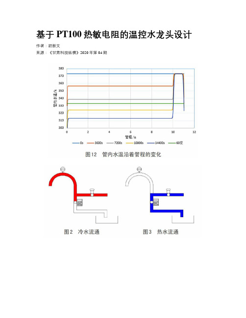
基于PT100热敏电阻的温控水龙头设计作者:胡新文来源:《甘肃科技纵横》2020年第04期摘要:基于PT100热敏电阻设计了一个低成本、高精度的温控电磁阀门开关,将之运用在普通热水水龙头上,以实现智能化控制水龙头可出热水的温度。
研究过程中对水龙头出水口管道进行了改进以提高分离冷水的能力。
最后进行实验来检测分析使用时水龙头口的热水温度误差,并利用软件模拟从锅炉到水龙头的水管内水温变化,来验证可节约的凉水的体积。
本设计结构精简、功能可靠,在日常生活中可以有效地控制水龙头“筛选”热水的能力,起到了节约水源的作用。
关键词:温度检测;热敏电阻;电压比较器;智能温控水龙头;引言目前,我国还是一个极度缺水的发展中国家,但经济建设和环保节约都不容忽视,二者兼顾发展变得日渐重要。
经调查发现,在学校、高速服务区等一些提供热水服务的地方,人们想要使用热水时,总会先打开水龙头让水流一会,等出口水温较高后再接水,而等待过程中的凉水就会流入下水道,这样就造成了水资源的大量浪费。
基于节约用水的理念,本设计利用现有成熟的电子元件产品,将之和传统的家用热水龙头结合,使改造后的水龙头可以流出满足需求温度的热水,而且让原管内的冷水回流并回收到储水器中。
在满足需求的同时又实现节约用水的功能,做到了生产低成本、节水高效益的实用价值。
1、设计方案1.1设计原理“智能温控回水龙头”是基于温度传感器进行一系列操控的。
测温触头被放置于出水管内部,测量待出水的温度。
如果测得的温度低于提前设置的期望温度,则单片机接受信号后判定为“凉水”,此时由电磁阀门控制的温控开关则打开,判定的“凉水”回流到储水器中。
凉水的流通路径如图2;如果测得的温度超过预设的期望温度,则单片机接受信号后判定为人们所需的“热水”,此时由电磁阀门控制的温控开关则关闭,“热水”从水龙头流出。
热水的流通路径如图3。
1.2设备的各部分原理1.2.1、温度传感器温度传感器是基于热电阻的反馈电路,其核心部分有PT100热电阻、LM339电压比较器、2N5551三极管以及Songle继电器。
基于OneNET的多模式远程控制开关系统设计
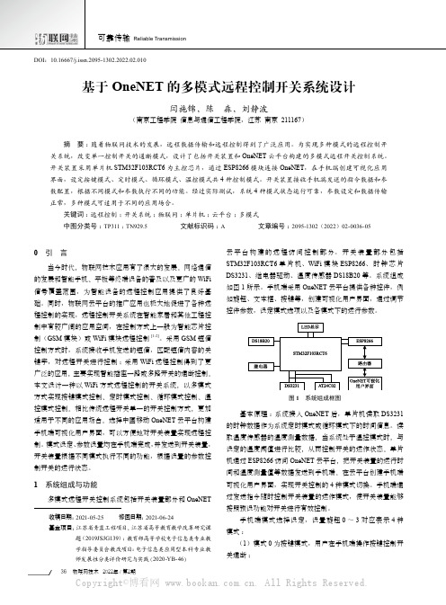
物联网技术 2022年 / 第2期360 引 言当今时代,物联网技术应用有了很大的发展。
网络通信的发展和智能手机、平板等终端设备的普及以及更广的WiFi 信号覆盖范围,为智能设备的远程控制应用提供了良好基础。
同时,物联网云平台的推广应用也极大地促进了各种远程控制的实现,远程控制开关系统在智能家居和其他工程控制中有较广阔的应用空间,在控制方式上一般为智能芯片控制(GSM 模块)或WiFi 模块远程控制[1-2]。
采用GSM 短信控制方式时,系统接收手机发送的短信,匹配短信内容的关键字,对远程开关进行控制;采用WiFi 远程控制得到了更广泛的应用,主要实现智能插座一路或多路开关的通断控制。
本文设计一种以WiFi 方式远程控制的开关系统,以多模式方式实现按键模式控制、定时模式控制、循环模式控制、温控模式控制。
相比传统远程开关单一的开关控制方式,更加适用于不同的应用场合。
选择中国移动OneNET 云平台构建手机端可视化用户界面,可以方便地对开关装置实现远程控制。
模式设定、参数设置均在手机端完成,并发送到开关装置,开关装置根据不同模式执行不同的功能,根据设置的参数控制开关的运行状态。
1 系统组成与功能多模式远程开关控制系统包括开关装置部分和OneNET云平台构建的远程访问控制部分。
开关装置部分包括STM32F103RCT6单片机、WiFi 模块ESP8266、时钟芯片DS3231、继电器驱动、温度传感器DS18B20等。
系统组成如图1所示。
手机端采用OneNET 云平台提供各种控件,例如旋钮、文本框、按键等,创建可视化用户界面,通过调节控件参数,设定模式选项以及各模式下的运行参数。
图1 系统组成框图基本原理:系统接入OneNET 后,单片机读取DS3231的时钟数据作为系统定时模式或循环模式下的时间信息。
读取温度传感器的温度测量数据,当系统处于温控模式时,与设定的温度阈值进行比较,从而控制开关的运作状态。
自动浇花系统的设计
题目自动浇花系统的设计学生姓名薛婵娟学号 ********** 所在学院物理与电信工程学院专业班级通信工程1201班指导教师刘亚锋完成地点物理与电信工程学院实验室2016年 6 月 5 日陕西理工学院本科毕业设计任务书院(系) 物理与电信工程学院专业班级通信工程(通信1201) 学生姓名薛婵娟一、毕业设计题目自动浇花系统的设计二、毕业设计工作自 2015 年 12 月 9 日起至 2016 年 6 月 18 日止三、毕业设计进行地点: 物理与电信工程学院实验室四、毕业设计应完成内容及相关要求:现代生活的节奏越来越快,很多人喜欢在工作地点、生活区间、公共场所等地方用绿色植物来点缀,既美化环境又能改善空气质量。
但对绿色植物的维护、保养是需要花不少时间去完成的,当由于种种原因忘记定时对花卉及时浇水时,或浇水的量过多或过少,反而会给人们带来很多麻烦和损失,因此设计一个家用自动浇花系统就十分必要。
本系统采用单片机为核心芯片,利用湿度传感器来采集土壤的湿度。
经过信息采集、信息比较、通过继电器控制信息,驱动水泵控制电路工作,实现自动浇花。
五、毕业设计应收集资料及参考文献:1、应收集与课题相关文献12篇(其中包括一篇英文文献),文献的发表年限应为2010年至2016年;2、除了文献之外,所参考的书目不能超过3篇;3、所有的参考资料要留存电子版,在交论文时一并打包交予指导教师。
六、毕业设计的进度安排:1、必须查阅大量资料(包括一定数量的外文资料),了解课题的研究背景、意义,熟悉设计中要用到的相关电路知识;完成开题报告;并完成一篇外文文献的全文翻译工作;(1月1日-3月18日)2、进行系统的概要设计;(3月19日-4月10日)3、熟悉设计软件,并提交中期报告;(4月10日-4月20日)4、系统的设计与实现;准备作品的验收;完成论文第一稿;(4月21日-5月10日)5、根据要求对对论文及作品进行完善,完成论文第二稿;(5月11日-5月20日)6、制作答辩PPT,准备答辩材料,准备答辩,并完成后续工作;(5月21日-6月10日)7、必须定期与指导老师见面,汇报进展情况,按时完成论文的撰写工作。
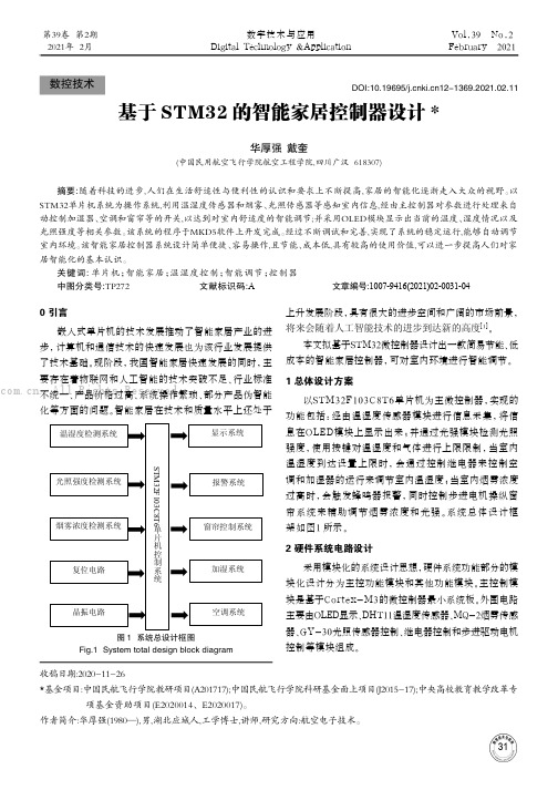
基于STM32的智能家居控制器设计★
310 引言嵌入式单片机的技术发展推动了智能家居产业的进步,计算机和通信技术的快速发展也为该行业发展提供了技术基础。
现阶段,我国智能家居快速发展的同时,主要存在着物联网和人工智能的技术突破不足、行业标准不统一、产品价格过高、系统操作繁琐、部分产品伪智能化等方面的问题。
智能家居在技术和质量水平上还处于上升发展阶段,具有很大的进步空间和广阔的市场前景,将来会随着人工智能技术的进步到达新的高度[1]。
本文拟基于STM32微控制器设计出一款简易节能、低成本的智能家居控制器,可对室内环境进行智能调节。
1 总体设计方案以STM32F103C8T6单片机为主微控制器,实现的功能包括:经由温湿度传感器模块进行信息采集,将信息在OLED模块上显示出来;并通过光强模块检测光照强度,使用按键对温湿度和气体进行上限限制,当室内温湿度到达设置上限时,会通过控制继电器来控制空调和加湿器的运行来调节室内温湿度;当室内烟雾浓度过高时,会触发蜂鸣器报警,同时控制步进电机操纵窗帘系统来辅助调节烟雾浓度和光强。
系统总体设计框架如图1所示。
2 硬件系统电路设计采用模块化的系统设计思想,硬件系统功能部分的模块化设计分为主控功能模块和其他功能模块。
主控制模块是基于Cortex-M3的微控制器最小系统板。
外围电路主要由OLED显示、DHT11温湿度传感器、MQ-2烟雾传感器、GY-30光照传感器控制、继电器控制和步进驱动电机控制等模块组成。
基于STM32的智能家居控制器设计*华厚强 戴奎(中国民用航空飞行学院航空工程学院,四川广汉 618307)摘要:随着科技的进步,人们在生活舒适性与便利性的认识和要求上不断提高,家居的智能化逐渐走入大众的视野。
以STM32单片机系统为操作系统,利用温湿度传感器和烟雾、光照传感器等感知室内信息,经由主控制器对参数进行处理来自动控制加湿器、空调和窗帘等的开关,以达到对室内舒适度的智能调节;并采用OLED模块显示出当前的温度、湿度情况以及光照强度等相关参数。
智能语音控制系统的设计与实现
智能语音控制系统的设计与实现王磊;何勇;张宇【摘要】In the future,it is an inevitable trend to combine the speech recognition with the intelligent control.Man-machine voice interaction provide a more user-friendly interface.In view of the speech recognition and the application of intelligent control,this paper puts forward a intelligent control design method based on speaker-independent speech recognition technology.It uses LD3320 chip to acquire and recognize speech information and STC10L08XE chip as the main controller to control the voice system,combined the external storage and the control circuitit realizes man-machine voice interaction and voice control.Design a voice interaction is different from the traditional control devices.It is easy to resolve a issue about how to modify the datas in external storage by designing an upper computer software.At the same time,it can write the voice data into the upper computer and configure parameters bined with the custom protocol frame,the data transmission process is more rapid,stable and reliable.According to repeated experimental verification,this speech control system works stably and owns excellent recognition rate.It is of great usability and market application value.%在未来的发展中,语音识别与自动化控制的结合也将是未来发展的一种必然趋势;语音交互方式是更为人性化的人机交互界面,针对语音识别与智能控制的运用,提出了一种基于非特定人语音识别技术的智能控制设计方法,并使用LD3320芯片将语音信息采集和识别,采用STC10L08XE芯片作为语音控制系统的主控制器,并结合外部存储器和控制电路实现人机语音交互和语音控制,设计一款区别于传统控制的语音交互设备;通过设计一款上位机软件,可以很好地解决外部存储器数据修改困难的问题,并同时进行实时的语音数据写入和参数配置,结合自定义的协议帧,使数据的传输过程更加快速、稳定和可靠,经过实验验证,该语音控制系统工作稳定、识别率高,具有很好的易用性和市场应用价值.【期刊名称】《计算机测量与控制》【年(卷),期】2018(026)002【总页数】4页(P109-112)【关键词】语音识别;非特定人;LD3320;语音控制;上位机【作者】王磊;何勇;张宇【作者单位】贵州大学计算机科学与技术学院,贵阳550000;贵州大学计算机科学与技术学院,贵阳550000;贵州大学计算机科学与技术学院,贵阳550000【正文语种】中文【中图分类】TN912.340 引言语言是人类沟通的桥梁,可以很轻松地达到信息的交互。