大功率开关电源板图纸
300w开关电源设计(图纸)

TND313/DRev 3, Sep-11High-Efficiency305 W ATX Reference Design Documentation Package© 2011 ON Semiconductor.Disclaimer: ON Semiconductor is providing this reference design documentation package “AS IS” and the recipient assumes all risk associated with the use and/or commercialization of this design package. No licenses to ON Semiconductor’s or any third party’s Intellectual Property is conveyed by the transfer of this documentation. This reference design documentation package is provided only to assist the customers in evaluation and feasibility assessment of the reference design. The design intent is to demonstrate that efficiencies beyond 80% are achievable cost effectively utilizing ON Semiconductor provided ICs and discrete components in conjunction with other inexpensive components. It is expected that users may make further refinements to meet specific performance goals.Table of Contents1.Overview (6)2.Specifications (7)3.Architecture Overview (8)4.Performance Results (13)5.Evaluation Guidelines (23)6.Schematics (24)7.Parts List (29)8.Critical Component Information (35)9.Resources/Contact Information (35)10.Appendix (36)List of TablesTable 1: Target Specifications (7)Table 2: Load matrix for efficiency measurements (13)Table 3: Load matrix for cross regulation measurements (15)Table 4: Transient load conditions (18)List of FiguresFigure 1: Reference Design Architecture Block Diagram (7)Figure 2: One switch forward topology and associated waveform (9)Figure 3: Active clamp forward topology and associated waveform (11)Figure 4: Efficiency vs percentage load from 20% to full load (13)Figure 5: Power factor vs percentage load (14)Figure 6: Efficiency vs percentage load from 5% to full load (14)Figure 7: 5 V and 5 V SBY outputs cross regulation vs load conditions (16)Figure 8: 3.3 V output cross regulation vs load conditions (16)Figure 9: 12 V1 and 12 V2 outputs cross regulation vs load conditions (17)Figure 10: -12 V output cross regulation vs load conditions (17)Figure 11: 5 V output transient load response (18)Figure 12: 12 V1 output transient load response (18)Figure 13: 12 V2 output transient load response (19)Figure 14: 3.3 V output transient load response (19)Figure 15: 5 V output voltage ripple at full load (20)Figure 16: 3.3 V output voltage ripple at full load (20)Figure 17: 12 V1 output voltage ripple at full load (20)Figure 18: 12 V2 output voltage ripple at full load (21)Figure 19: -12 V output voltage ripple at full load (21)Figure 20: 5 V SBY output voltage ripple at full load (21)Figure 21: Holdup time at full load (22)Figure 22: Input inrush current (22)Figure 23: ATX solution boards in ATX enclosure (24)Figure 24: PFC controller PCB board schematic (25)Figure 25: EMC component board (25)Figure 26: Active clamp controller PCB board schematic (26)Figure 27: Supervisory and 3.3 V post regulator controller PCB board schematic (27)Figure 28: Main PCB board schematic PFC and standby section (27)Figure 29: Main PCB board schematic active clamp stage section (28)Figure 30: Main PCB board schematic 3.3 V post regulator section (28)1. OverviewON Semiconductor was the first Semiconductor company to provide an 80 PLUS open reference design for an ATX Power Supply in 2005. This 1st generation reference design, was certified and met all the requirements of the 80 PLUS program. Following on this successful 1st generation design, ON Semiconductor is introducing its improved 2nd Generation reference design. This 2nd generation design utilizes newer ICs from ON Semiconductor that enable this design to exceed 80% efficiency starting at 20% load across different line conditions with ample margin to spare.This reference document provides the details behind this 2nd generation design. The design manual provides a detailed view of the performance achieved with this design in terms of efficiency, performance, thermals and other key parameters. In addition, a detailed list of the bill-of-materials (BOM) is also provided. ON Semiconductor will also be able to provide technical support to help our customers design and manufacture a similar ATX power supply customized to meet their specific requirements.The results achieved in this 2nd generation design were possible due to the use of advanced new components from ON Semiconductor. These new ICs not only speeded up the overall development cycle for this new design, but also helped achieve the high efficiencies while at the same time keeping a check on the overall cost. With the use of these new ICs, ON Semiconductor has proven again that the emerging requirements for high efficiency desktop power supplies can be met and further, can be optimized to meet specific performance vs. cost goals.This 2nd generation design consists of a single PCB designed to fit into the standard ATX enclosure along with a fan. Figure 1 below presents the overall architecture employed in this design – detailed schematics are included later in this design manual. As seen in figure 1, this design employed an Active Clamp forward topology using the new, highly integrated Active Clamp Controller IC from ON Semiconductor – NCP1562. A Continuous Conduction Mode (CCM) Power Factor Correction (PFC) IC was employed for the active PFC circuit. This IC, the NCP1653 provides an integrated, robust and cost-effective PFC solution. The standby controller, NCP1027, is an optimized IC for the ATX power supply and incorporates a high-voltage MOSFET. On the secondary side, this architecture employs a post regulator approach for generating the 3.3 V output. This is an alternative approach to the traditional magnetic amplifier (Mag Amp) approach. Though ON Semiconductor believes that this post regulator approach provides the highest efficiency amongst the different means of generating these outputs in the power supply, it is important to note that if the customer desires to use a different approach, that is possible – i.e. a similar design can be developed that utilizes all the other pieces of this architecture without the post regulator and still achieve very good results.With the introduction of this 2nd generation, high-efficiency ATX Power Supply, ON Semiconductor has shown that with judicious choice of design tradeoffs, optimum performance is achieved at minimum cost.Figure 1: Reference Design Architecture Block Diagram2. SpecificationsThe design closely follows the ATX12V version 2.2 power supply guidelines and specifications available from , unless otherwise noted. For instance, our reference design had a target of +/- 5% tolerance for both the 5 V and 5 Vstandby outputs. Further, the efficiency targets for the 80 PLUS program and the EPA’s Energy Star specification – Energy Star Program Requirements for Computers, version 4.0 that is set to take effect from July 20, 2007 – were targeted. Key specifications are included in Table 1 below.Output Current Tolerance (%) Ripple/Noise(mV) Min. (A) Max (A)5 V 0.3 22 ± 3.350 5 V standby 0.0 2.5 ± 3.350 12 V 1.0 18 ± 5.0120 - 12 V 0.0 1 ± 10120 Table 1: Target SpecificationsTarget specifications for other key parameters of the reference design include: -Efficiency: Minimum efficiency of 80% for 20%, 50% and 100% of rated output load conditions as defined by the 80 PLUS requirements as well as the Energy Star specification.-Power Factor: Power factor of 0.9 or greater at 100 % load.-Input Voltage: Universal Mains – 90 Vac to 265 Vac, 47 – 63 M Hz.-Output Power: Total maximum output power is 305 W.-Safety Features: As per the ATX12V specification, this design includes safety features such as OVP, UVP, and OCP.-This design meets the IEC1000-3-2 requirements over the input line range and under full load conditions.-This converter was designed for a 20 ms minimum Hold-up time.-Physical dimensions: This converter is designed to fit into the standard ATX enclosure with dimensions of 150 mm x 140 mm x 86 mm.3. Architecture OverviewBefore discussing the power supply architecture of the Generation 2 design, it is worth reiterating the design goals. We are tasked with providing a flexible power platform, which is required to have the lowest cost and highest efficiency that can be packaged in a small volume. The architecture must deliver a minimum of 80% efficiency over a wide range of operating conditions (high-line and low-line) as well as rated output load conditions (20% load and above). In addition we require a robust design solution having low parts count to provide the same performance on a unit to unit basis in a high volume manufacturing environment.The architecture selected follows a traditional two stage conversion approach as illustrated in Figure 1. It is worth noting that in order to achieve 80% efficiency overall, the efficiency of each of the two conversion stages must exceed 90 %. The front-end is a universal input, active power factor boost stage delivering a constant output voltage of 385 V to the active clamp stage. The second stage consists of two, dc-dc converters. The first down-stream converter processes 290 W required by the system in the form of tightly regulated +/-12 V, +5 V and +3.3 V outputs. The second converter delivers 15 W of standby power to another isolated 5 V rail.ON Semiconductor has developed multiple power management controllers and MOSFET devices in support of the ATX program. Web based data sheets, design tools and technical resources are available to assist design optimization. The ICs, supporting the ATX Generation 2 platform, are the NCP1653 PFC controller, the NCP1562 active clamp controller, the NCP4330 post regulator, the NCP1027 standby controller, and the NTP48xx family of MOSFET synchronous rectifiers. It is not possible to discuss the tradeoffs involved in each conversion stage at length, but the selection of the activeclamp forward converter topology is a key one and will be covered in depth. Each controller is highly integrated and offers the lowest external parts count available.PFC StageThere are a variety of PFC topologies available. These include discontinuous conduction mode (DCM), critical conduction mode (CRM) and continuous conduction mode (CCM). At this power level, CCM is the preferred choice and the NCP1653 will implement a IEC1000-3-2 compliant, fixed frequency, peak current mode PFC boost converter with very few external components.DC to DC (Main) ConverterThe selection of the dc-dc down stream converter is at the heart of the 80% solution. The traditional work horse of the ATX market has been the single switch forward converter operating at a switching frequency of 100 kHz. The converter and its associated drain waveform are illustrated in Figure 2. This topology is robust and delivers good full load efficiency performance at minimal cost. However, as power levels increase and regulatory requirements and energy conservation agencies drive for higher efficiency under all load conditions, the single switch forward topology in its simplest form is reaching its limit.Figure 2: One switch forward topology and associated waveformThere are several technical reasons for this. First, because the main transformer is reset via an auxiliary winding across the input bus, the duty cycle is limited below 50%. Second, because of this reset mechanism there is always a dead time interval, during each converter cycle, when no power is flowing. These two constraints have negative implications on the silicon utilization of the primary switch requiring a costly, large area die to be selected. The primary switch’s conduction loss is given by (1))(*2*)(on DS R P I D conduction loss P =(1)where, D is the duty cycle, I P is the primary current and R DS(on) is the switch on resistance. The topology is a hard switched topology with the primary switch being driven on with 385 V across it each switching cycle. The capacitive switch loss are given by (2),f DS V OSS C capacitive loss P *2*21)(= (2)where, C OSS is the switch output capacitance, V DS is the drain to source voltage and f is the operating frequency. Capacitive losses dominate at light load. Hence a switch selected for full load performance will suffer at light load because of its large drain source capacitance. Reviewing these two loss equations, it becomes apparent for efficiency enhancement under both full load and light load operation, a topology is required that allows the primary switch to operate at lower current and voltage stress. As the loss terms appear as current and voltage squared, small reductions in primary current I P and switch voltage V DS significantly improve performance.The active clamp forward converter illustrated in Figure 3 represents the ultimate extension of the single switch converter and provides these benefits. Instead of using an auxiliary winding, transformer reset is achieved using a clamp capacitor and an auxiliary switch. The reset period, controlled by the auxiliary switch now extends to the interval ()S T D *1−, completely eliminating the previous dead time interval. To maintain flux balance in the main transformer core, the reset voltage across the clamp capacitor isdetermined by the expression ()D D in V −1*. The duty cycle D of the single switch forwardconverter can extend beyond 50%, limited only by the primary switch’s maximum voltage rating.Figure 3: Active clamp forward topology and associated waveformFor a given set of conditions and power throughput, operating at extended duty cycles allows for a lower primary current. This in turn allows the selection of a smaller, lower cost die. Let’s look at a design example to illustrate this point.To reduce cost, a 150 μF bulk capacitor (instead of a 470 μF conventional value) is selected to provide 20 ms of hold up time. Using the energy storage equation given by (3),()ηtime up Hold Delivered Power V V C Energy f i **2122=−= (3)where, V i and V f are the initial and final voltages of the input capacitor, respectively. The initial voltage is 385 V and converter efficiency is 90%, allows us to calculate the final voltage V f to be 250 V. In the case of a conventional single switch design, the maximum duty cycle we can practically select and avoid transformer saturation is 0.45. The switch voltage stress is 2 x 250 V. With the active clamp single switch forward, the duty cycle can be extended to 0.67 and the voltage stress on the switch is Vin / (1-D) or 3.03 x 250 V. Each converter has to process 290 / 0.9 or 322 W from the primary bulk source. At nominal 385 V bulk, the average primary current is 0.84 A. Factoring in the primary switch duty cycle D, the peak current I P in the traditional forward converter is 0.65 / 0.45 or 1.44 times larger than the active clamp approach. Based on the conduction loss equation given by (1), we see that the 1.44 ratio holds true for conduction loss in the primary switch. Put another way, we can choose a MOSFET with 44% higher R DS(on) in the active clamp topology and have the same conduction loss. This is significant, as we can achieve better silicon utilization, lower cost and lower drain capacitance. By reviewing the data sheets from high voltage MOSFET vendors, it is possible to compare output capacitance C OSS versus R DS(on) as a function of die size. For example as MOSFET resistance increases from 3.6 Ω to 4.8 Ω, the output capacitance reduces from100 pF to 70 pF. The resonant nature of the active clamp allows the switch be turned on at 300 V instead of the conventional 400 V. These two effects allow a reduction in capacitive switching loss of 39% over a conventional design. Again, a significant improvement remembering that light load efficiency is determined predominately by switching loss. The example above illustrates how small changes in switch stress can impact overall cost and performance.The same argument relating to increased duty cycle operation extends to the secondary by proportionally reducing output rectifier loss. Since the secondary loss is a dominant factor at full load, an additional efficiency improvement/ cost benefit is realized. To achieve the ultimate efficiency, synchronous rectification is required on the +12 V and +5 V outputs. The single switch active clamp forward is very suitable to drive synchronous rectifiers directly from the secondary windings without the need for expensive gate drivers or additional delay timing circuitry.To allow designers to capitalize on the benefits inherent in the active clamp topology, the NCP1562 has been developed to capture all the necessary control features within a 16 pin package. The full featured controller has been designed for tight tolerance on all parameters, including the maximum duty cycle limit and the important soft stop function. To boost efficiency and maintain tight regulation, instead of the conventional magnetic amplifier post regulated approach, the 3.3 V output is derived from the 5 Volt winding of the main transformer. The MOSFET drivers, timing, synchronization and control functions to support this output are provided by the NCP4330 controller. A 6 W improvement in the loss budget is achieved when this approach is adopted. Gate charge and R DS(on) have been optimized in the NTP48xx family of MOSFETs and provide synchronous rectification for both the 3.3 V and 5 V outputs.Standby PowerThe NCP1027 integrates a fixed frequency current mode controller and a 700 volt MOSFET. The NCP1027 is an ideal part to implement a flyback topology delivering 15 W to an isolated 5 V output. At light loads the IC will operate in skip cycle mode, thereby reducing its switching losses and delivering high efficiency throughout the load range.4. Performance ResultsThe evaluation of the reference design focused on several areas including efficiency, power factor, cross regulation and transient load response. Design optimizations may be needed to customize this reference design to meet specific requirements.The converter efficiency is measured according to the operating conditions detailed in Table 2. The converter efficiency is measured at 100 Vac, 115 Vac and 230 Vac at 50 Hz. The converter achieves over 80% efficiency with room to spare over all load conditions as shown in Figure 4. The output voltages used for the efficiency calculations are measured at the end of the power cables. The fan is disabled for measurements at or below 20% load. The fan is automatically enabled once the load exceeds 60 W or 20%. The fan is operational for 50% and 100% load measurements. Further increases in the efficiency can be obtained for 50% and 100% load conditions through fan speed control.Load Condition Output Current (A) 5 V 3.3 V 12 V1 12 V2 -12V5 V SBY 5 % 0.690 0.540 0.385 0.385 0.030 0.070 10 % 1.390 1.070 0.770 0.770 0.070 1.390 15 % 2.080 1.610 1.150 1.150 0.100 0.210 20 % 2.7802.150 1.510 1.510 0.140 0.280 50 % 6.950 5.3703.845 3.845 0.350 0.700 100 %13.900 10.7407.695 7.6950.700 1.400Figure 4: Efficiency vs percentage load from 20% to full loadThe power factor exceeds 0.9 over all operating conditions as shown in Figure 5.Figure 5: Power factor vs percentage loadIn Figure 6, the efficiency measurements are shown from 5% load to full-load. Note that neither the 80 PLUS program nor the Energy Star specification require efficiencies above 80% for any output load below 20%. However, as can be seen in Figure 6, this reference design achieved 80% efficiency down to 16 % load.Figure 6: Efficiency vs percentage load from 5% to full loadOutput voltage cross regulation is measured according to the load conditions listed in Table 3. The results of the cross regulation measurements are shown inFigure 7 through Figure 10. Included in these figures are the tolerance requirements based on the target specifications listed in Table 1. The margin for the 5 V and 5 V SBY outputs can be increased by shifting up the regulation target for the 5 V outputs. It can also be improved by changing the weight of the 12 V and 5 V outputs in the regulation circuit.Load ConditionOutput Current (A)5 V(+/-3.3%)3.3 V(+/-4%)12 V1(+/-5%)12 V2(+/-5%)-12 V(+/-10%)5 V SBY(+/-3.3%)1 0.3 0.3 0 0 0 02 73 2 2 0.1 0.53 0.3 0.3 0 0 0 0.54 0.3 3 2 2 0.1 0.55 7 0.3 2 2 0.1 0.56 4 0.3 1 1 0.2 0.27 18 12 5 5 1 2.58 18 12 1 1 0.2 2.59 4 12 5 5 1 2.510 18 0.3 5 5 1 2.511 4 0.2 1 1 0.2 0.212 14 17 8 6 1 2.513 18 17 1 1 0.2 2.514 4 17 8 6 1 2.515 18 0.3 8 6 1 2.516 4 2 5 5 0.2 117 22 17 5 5 1 2.518 4 17 5 5 1 2.519 22 2 5 5 1 2.5Table 3: Load matrix for cross regulation measurementsFigure 7: 5 V and 5 V SBY outputs cross regulation vs load conditionsFigure 8: 3.3 V output cross regulation vs load conditionsFigure 9: 12 V1 and 12 V2 outputs cross regulation vs load conditionsFigure 10: -12 V output cross regulation vs load conditionsThe 5 V, 12 V and 3.3 V outputs are evaluated independently under transient load conditions. Each output is loaded at 50% and the load is reduced to 25% or increased to 75% of the maximum rated current. The transient voltage tolerance of each of the 5 V, 12 V and 3.3 V outputs is +/- 5%. Table 4 summarizes the transient load conditions and limits for each output. Transient waveforms are shown in Figure 11 through Figure 14.Output Minimum Load (A)Nominal Load (A)Maximum Load (A)Voltage under/overshoot (V) 5 V 5.5 11 16.5 ±250mV, ≤0.5V pk-pk 3.3 V 4.25 8.5 12.75 ±170mV, ≤0.34V pk-pk 12 V1 4.5 9 13.5 ±600mV, ≤1.2V pk-pk 12 V24.5913.5±600mV, ≤1.2V pk-pkTable 4: Transient load conditionsFigure 11: 5 V output transient load responseFigure 12: 12 V1 output transient load responseΔI LOAD = 11.5 A to 5.5 AΔI LOAD = 11.5 A to 16.5 AΔI LOAD = 9 A to 4.5 AΔI LOAD = 9 A to 13.5 AFigure 13: 12 V2 output transient load responseFigure 14: 3.3 V output transient load responseAll the outputs meet the transient voltage requirements under the evaluated conditions. The ripple voltage of each output is measured at the maximum load for each output. The output ripple is measured across 10 μF/MLC parallel 1000 μF low ESR/ESL termination capacitors. The target ripple is +/- 120 mV for the 12 V outputs and 50 mV for all other outputs. Figure 15 through Figure 20 show the output voltage ripple measurements. All outputs meet the voltage ripple requirements.ΔI LOAD = 9 A to 4.5 AΔI LOAD = 9 A to 13.5 AΔI LOAD = 8.5 A to 4.25 AΔI LOAD = 8.5 A to 12.75 AFigure 15: 5 V output voltage ripple at full loadFigure 16: 3.3 V output voltage ripple at full loadFigure 17: 12 V1 output voltage ripple at full loadFigure 18: 12 V2 output voltage ripple at full loadFigure 19: -12 V output voltage ripple at full loadFigure 20: 5 V SBY output voltage ripple at full loadThe required holdup time at full load is 20 ms. Holdup time is measured from the moment the AC power is removed to when the PWR_OK signal goes low. Figure 21 shows the holdup time at full load. Channel 1 is the AC power and Channel 2 is the PWR_OK signal. Holdup time is measured at 22.5 ms.Figure 21: Holdup time at full loadThe input inrush current of the system at 230 Vac at full load is measured at 28.8 A as shown in Figure 22.Figure 22: Input inrush current5. Evaluation GuidelinesEvaluation of the reference design should be attempted only by persons who are intimately familiar with power conversion circuitry. Lethal mains referenced voltages and high dc voltages are present within the primary section of the ATX circuitry. All testing should be done using a mains high-isolation transformer to power the demonstration unit so that appropriate test equipment probing will not affect or potentially damage the test equipment or the ATX circuitry. The evaluation engineer should also avoid connecting the ground terminal of oscilloscope probes or other test probes to floating or switching nodes (e.g. the source of the active clamp MOSFET). It is not recommended to touch heat sinks, on which primary active components are mounted, to avoid the possibility of receiving RF burns or shocks. High impedance, low capacitance test probes should be used where appropriate for minimal interaction with the circuits under investigation. Particular care should be taken when probing the high impedance input pins of the NCP1653 power factor controller and the NCP1562 active clamp controller. As with all sensitive switchmode circuitry, the power supply under test should be switched off from the ac mains whenever the test probes are connected and/or disconnected.The 3.3 V output does not have a minimum load requirement and a preload resistor is included in the -12 V output.The NCP1027 standby flyback converter will be operational as long as there is ac mains voltage applied to the system. This auxiliary converter can be evaluated by merely applying the mains voltage to the board. The supervisory IC enable input and monitoring circuitry will have to be disabled. The supervisory circuitry will normally cause a shutdown of the PFC (and the main converter) if the 3.3 V, the 5 V and the 12 V outputs are not sensed at their nominal voltage.The evaluating engineer should also be aware of the idiosyncrasies of constant current type electronic loads when powering up the ATX demonstration unit. If the loads are adjusted to be close to the ATX’s maximum rated output power, the unit could shut down at turn on due to the instantaneous overloading effect of the constant current loads. As a consequence, electronic loads should be set to constant resistance mode or rheostats should be used for loads. The other alternative is to start the supply at light to medium load and then increase the constant current electronic loads to the desired level.The board is designed to fit in a traditional ATX enclosure as shown in Figure23.Figure 23: ATX solution boards in ATX enclosure6. SchematicsThe power supply is implemented using a single sided PCB board. Added flexibility is provided by using daughter cards for the PFC (NCP1653), active clamp (NCP1562) controllers. A PCB board is also used for the 3.3 V post regulator (NCP4330) and supervisory controllers. This allows the use of newer generation controllers without the need of a complete re-layout of the main board. An additional daughter card is used for EMC components. The individual PCB board schematics are shown in Figure 24 through Figure 27.The schematic of the main PCB board is divided in three sections: PFC & standby section, active clamp section, and the post regulator section as shown in Figure 28 through Figure 30, respectively.Figure 24: PFC controller PCB board schematicFigure 25: EMC component boardFigure 27: Supervisory and 3.3 V post regulator controller PCB board schematicFigure 28: Main PCB board schematic PFC and standby sectionFigure 29: Main PCB board schematic active clamp stage sectionFigure 30: Main PCB board schematic 3.3 V post regulator section7. Parts ListThe bill of materials (BOM) for the design is provided in this section. To reflect theschematics shown in the previous section, the BOM have also been broken into differentsections and provided in separate tables – Table 5 through Table 9.It should be noted that a number of components used during the development cycle werebased on availability. As a result, further cost reductions and better inventorymanagement can be achieved by component standardization. IE, the unique part numberscan be SIGNIFICANTLY reduced by standardization and re-use of component valuesand case sizes. This will result in a lower cost BOM and better inventory management.Description Part Numbers Qty 0.1µF, ±10%, 500V, X7R, Case Size 1812 VJ1812Y104KXEAT 3 0.1µF, ±10%, 50V, X7R, Case Size1206 B37872K5104K060 18 0.1µF, ±20%,300VAC, Interference Suppression CapX2 PHE840EB6100MB05R17 2 0.22uF, ±20% ,300VAC, Interference Suppression CapX2 PHE840EX6220MB06R17 1 270µF, ±20%, 400V, -40°C to +85°C, B43501 series , Snap-In, Pitch 10mm B43501A9277M000 1 100pF, ±10%, 1kVDC,High voltage ceramic disc Capacitor, -25°C to +85°C DEBB33A101KC1B 2 100pF, ±5%, 50V, COG, Case Size1206 B37871K5101J060 1 1nF, ±20% , 100V , Stacked-film capacitor, MMK series , 5mm Pitch MMK5 102M100J01L4 BULK 2 1nF, ±10%, 1kVDC,High voltage ceramic disc Capacitor,-25°C to +85°C DEBB33A102KA2B 2 1nF, ±20%,, 440VAC,Interference Suppression CapY1 PME294RB4100MR30 2 1nF,±20%, ,440/250VAC,Interference Suppression CapX1/Y2 2252 812 35 027 1 1nF, ±10%, 100V, COG, Case Size1206 B37871K1102J560 5 4.7nF, ±10%, 1kVDC, High voltage ceramic disc Capacitor, -25°C to +85°C DEBB33A472KA3B 1 4.7nF,±10% ,440/250VAC,Interference Suppression CapX1/Y2 2252 812 35 427 1 10nF, ±20% , 100V , Stacked-film capacitor, MMK series , 5mm Pitch MMK5 103M100J01L4 BULK 1 10nF, ±10%, 50V, X7R, Case Size1206 B37872K5103K060 1 22nF, ±20% , 100V , Stacked-film capacitor, MMK series , 5mm Pitch MMK5 223M100J01L4 BULK 1 2n2F, ±5%, 50V, COG, Case Size1206 B37871K5222J060 1 470pF, ±5%, 50V, COG, Case Size1206 B37871K5471J060 1 10µF, ±20%, 16V,-40°C to +85°C, Type VR, Radial, Pitch 2mm, Pb Free UVR1C100MDD 4 220µF, ±20%, 25V,-40°C to +85°C, Type VR, Radial, Pitch 3.5mm, Pb Free UVR1E221MPD 1 3300µF, ±20%, 10V,-40°C to +85°C, Type VR, Radial, Pitch 5mm, Pb Free UVR1A332MHD 1 47µF, ±20%, 25V,-40°C to +85°C, Type VR, Radial, Pitch 2mm, Pb Free UVR1E470MDD 1 2200µF, ±20%, 10V,-40°C to +85°C, Type PM, Radial, Pitch 5mm, Pb Free UPM1A222MHD 2 220µF, ±20%, 25V,-40°C to +85°C, Type PW, Radial, Pitch 3.5mm, Pb Free UPW1E221MPD 2 470E, ±1%, 0.25W, Case Size 1206 MCR18 EZH F-4700 1 0.2E, ±1%,1W, Case Size 2010 CRL1206-FW-0R20E_ 3 0E022, ±5%, 3W,Wire Wound Resister BSI680E022±5%±100ppm/°C 1 100E, ±1%, 0.25W, Case Size 1206 MCR18 EZH F-1000 1 100E, ±1%, 0.25W, MFR EROS2CHF1000 2 10E0, ±1%, 0.25W, Case Size 1206 MCR18 EZH F-10R0 2 10E, ±1%, 0.5W, Case Size 2010 MCR50-JZH-J 10R0 5。
常见几种开关电源工作原理及电路图

常见几种开关电源工作原理及电路图图二开关电源基本电路框图开关式稳压电源的基本电路框图如图二所示。
交流电压经整流电路及滤波电路整流滤波后,变成含有一定脉动成份的直流电压,该电压进人高频变换器被转换成所需电压值的方波,最后再将这个方波电压经整流滤波变为所需要的直流电压。
控制电路为一脉冲宽度调制器,它主要由取样器、比较器、振荡器、脉宽调制及基准电压等电路构成。
这部分电路目前已集成化,制成了各种开关电源用集成电路。
控制电路用来调整高频开关元件的开关时间比例,以达到稳定输出电压的目的。
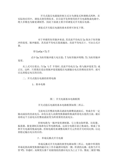
2.单端反激式开关电源单端反激式开关电源的典型电路如图三所示。
电路中所谓的单端是指高频变换器的磁芯仅工作在磁滞回线的一侧。
所谓的反激,是指当开关管VT1 导通时,高频变压器T初级绕组的感应电压为上正下负,整流二极管VD1处于截止状态,在初级绕组中储存能量。
当开关管VT1截止时,变压器T初级绕组中存储的能量,通过次级绕组及VD1 整流和电容C滤波后向负载输出。
单端反激式开关电源是一种成本最低的电源电路,输出功率为20-100W,可以同时输出不同的电压,且有较好的电压调整率。
唯一的缺点是输出的纹波电压较大,外特性差,适用于相对固定的负载。
单端反激式开关电源使用的开关管VT1 承受的最大反向电压是电路工作电压值的两倍,工作频率在20-200kHz之间。
3.单端正激式开关电源单端正激式开关电源的典型电路如图四所示。
这种电路在形式上与单端反激式电路相似,但工作情形不同。
当开关管VT1导通时,VD2也导通,这时电网向负载传送能量,滤波电感L储存能量;当开关管VT1截止时,电感L通过续流二极管VD3 继续向负载释放能量。
在电路中还设有钳位线圈与二极管VD2,它可以将开关管VT1的最高电压限制在两倍电源电压之间。
为满足磁芯复位条件,即磁通建立和复位时间应相等,所以电路中脉冲的占空比不能大于50%。
由于这种电路在开关管VT1导通时,通过变压器向负载传送能量,所以输出功率范围大,可输出50-200 W的功率。
常见几种开关电源工作原理及电路图

常见几种开关电源工作原理及电路图————————————————————————————————作者:————————————————————————————————日期:一、开关式稳压电源的基本工作原理开关式稳压电源接控制方式分为调宽式和调频式两种,在实际的应用中,调宽式使用得较多,在目前开发和使用的开关电源集成电路中,绝大多数也为脉宽调制型。
因此下面就主要介绍调宽式开关稳压电源。
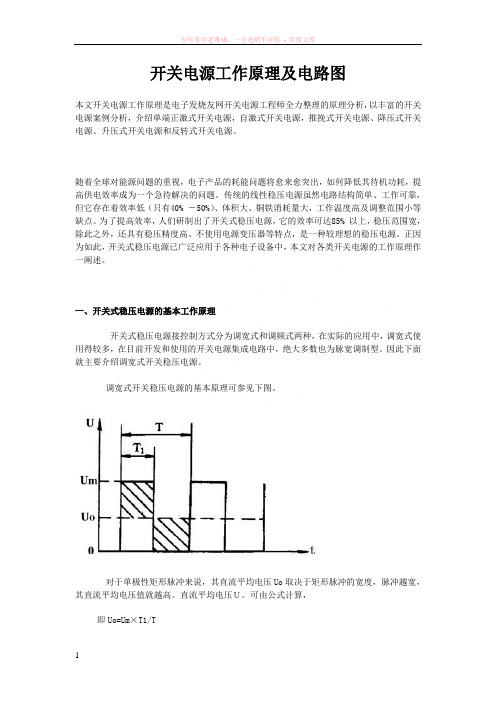
调宽式开关稳压电源的基本原理可参见下图。
对于单极性矩形脉冲来说,其直流平均电压Uo取决于矩形脉冲的宽度,脉冲越宽,其直流平均电压值就越高。
直流平均电压U。
可由公式计算,即Uo=Um×T1/T式中Um为矩形脉冲最大电压值;T为矩形脉冲周期;T1为矩形脉冲宽度。
从上式可以看出,当Um 与T 不变时,直流平均电压Uo 将与脉冲宽度T1 成正比。
这样,只要我们设法使脉冲宽度随稳压电源输出电压的增高而变窄,就可以达到稳定电压的目的。
二、开关式稳压电源的原理电路1、基本电路图二开关电源基本电路框图开关式稳压电源的基本电路框图如图二所示。
交流电压经整流电路及滤波电路整流滤波后,变成含有一定脉动成份的直流电压,该电压进人高频变换器被转换成所需电压值的方波,最后再将这个方波电压经整流滤波变为所需要的直流电压。
控制电路为一脉冲宽度调制器,它主要由取样器、比较器、振荡器、脉宽调制及基准电压等电路构成。
这部分电路目前已集成化,制成了各种开关电源用集成电路。
控制电路用来调整高频开关元件的开关时间比例,以达到稳定输出电压的目的。
2.单端反激式开关电源单端反激式开关电源的典型电路如图三所示。
电路中所谓的单端是指高频变换器的磁芯仅工作在磁滞回线的一侧。
所谓的反激,是指当开关管VT1 导通时,高频变压器T初级绕组的感应电压为上正下负,整流二极管VD1处于截止状态,在初级绕组中储存能量。
当开关管VT1截止时,变压器T初级绕组中存储的能量,通过次级绕组及VD1 整流和电容C滤波后向负载输出。
开关电源工作原理及电路图
开关电源工作原理及电路图本文开关电源工作原理是电子发烧友网开关电源工程师全力整理的原理分析,以丰富的开关电源案例分析,介绍单端正激式开关电源,自激式开关电源,推挽式开关电源、降压式开关电源、升压式开关电源和反转式开关电源。
随着全球对能源问题的重视,电子产品的耗能问题将愈来愈突出,如何降低其待机功耗,提高供电效率成为一个急待解决的问题。
传统的线性稳压电源虽然电路结构简单、工作可靠,但它存在着效率低(只有40% -50%)、体积大、铜铁消耗量大,工作温度高及调整范围小等缺点。
为了提高效率,人们研制出了开关式稳压电源,它的效率可达85% 以上,稳压范围宽,除此之外,还具有稳压精度高、不使用电源变压器等特点,是一种较理想的稳压电源。
正因为如此,开关式稳压电源已广泛应用于各种电子设备中,本文对各类开关电源的工作原理作一阐述。
一、开关式稳压电源的基本工作原理开关式稳压电源接控制方式分为调宽式和调频式两种,在实际的应用中,调宽式使用得较多,在目前开发和使用的开关电源集成电路中,绝大多数也为脉宽调制型。
因此下面就主要介绍调宽式开关稳压电源。
调宽式开关稳压电源的基本原理可参见下图。
对于单极性矩形脉冲来说,其直流平均电压Uo取决于矩形脉冲的宽度,脉冲越宽,其直流平均电压值就越高。
直流平均电压U。
可由公式计算,即Uo=Um×T1/T式中Um为矩形脉冲最大电压值;T为矩形脉冲周期;T1为矩形脉冲宽度。
从上式可以看出,当Um 与T 不变时,直流平均电压Uo 将与脉冲宽度T1 成正比。
这样,只要我们设法使脉冲宽度随稳压电源输出电压的增高而变窄,就可以达到稳定电压的目的。
二、开关式稳压电源的原理电路1、基本电路图二开关电源基本电路框图开关式稳压电源的基本电路框图如图二所示。
交流电压经整流电路及滤波电路整流滤波后,变成含有一定脉动成份的直流电压,该电压进人高频变换器被转换成所需电压值的方波,最后再将这个方波电压经整流滤波变为所需要的直流电压。
开关电源制作设计(电路原理图+PCB)

一、工作原理我们先熟悉一款开关电源的工作原理,该电源可输出5V电压,如图1所示。
1. 抗干扰电路在电网输入端首先设置一个NTC5D-9负温度系数热敏电阻,作用是保护后面的整流桥,刚开机时热敏电阻处于冷态,阻值比较大,可以限制输入电流,正常工作时,电阻比较小。
这样对开机时的浪涌电流起到有效的缓冲作用。
电容CY1、CY2、CY3、CY4用以滤除从工频电网上进入开关稳压电源和从开关稳压电源进入工频电网的不对称杂散信号,电容CX1、CX2用以滤除从工频电网上进入开关稳压电源和从开关稳压电源进入工频电网的对称杂散信号,用电感L1抑制从工频电网上进入开关稳压电源和从开关稳压电源进入工频电网的频率相同、相位相反的杂散干扰电流信号。
采用高频特性好的瓷片电容和铁芯电感,实现开关稳压电源电路中的高频辐射不污染工频电网和工频电网上的杂散电磁波不会窜入开关稳压电源电路中而干扰和影响其工作,对高频分量或工频的谐波分量具有急剧阻止通过功能,而对于几百赫兹以下的低频分量近似一条短路线。
图1 开关电源的工作原理图2. 整流滤波电路在电路中D1、D2、D3、D4组成全桥整流电路,把输入的交流电压进行全波整流,然后用C1进行滤波,最后变成直流输出供电电压,为后级的功率变换器供电,整流滤波后的电压约为300V。
3. UC3842供电与振荡300V的脉动直流电压,此电压经R12降压后给C4充电,供电UC3842的7脚,当C4的电压达到UC3842的启动电压门槛值时,UC3842开始工作并提供驱动脉冲,由6脚输出推动开关管工作。
一旦开关管工作,反馈绕组的能量经过D6整流,C4滤波,又供电到UC3842的7脚,这时可以不需要R12的启动了。
C9、R11接UC3842的定时端,和内部电路构成振荡电路,振荡的工作频率计算为:f=1.8/(Rt*Ct)代入数据可计算工作频率:f=68.18K4. 稳压电路该电路主要由精密稳压源T L 4 3 1 和线性光耦P C 8 1 7 组成,假设输出电压↑→经过R 1 6 、R 1 9 、R20、RES3的取样电压↑→TL431的1脚电压↑,当该脚电压大于TL431的基准电压2.5V时,TL431的2、3脚导通,→通过光电耦合到UC3842的2脚,于是UC3842的6脚驱动脉冲的占空比↓→开关变压器T1绕组上的能量↓→输出电压↓,达到稳压作用;反之,假设输出电压下降,则稳压过程与上相反。
开关电源电路图及原理讲解
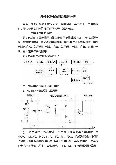
开关电源电路图及原理讲解最近一段时间很多朋友问到关于强电问题,其中关于开关电路居多,那么今天我们来详细了解下关于电路的接法。
一、开关电源的电路组成开关电源的主要电路是由输入电磁干扰滤波器(EMI)、整流滤波电路、功率变换电路、PWM控制器电路、输出整流滤波电路组成。
辅助电路有输入过欠压保护电路、输出过欠压保护电路、输出过流保护电路、输出短路保护电路等。
开关电源的电路组成方框图如下:二、输入电路的原理及常见电路1、AC输入整流滤波电路原理:①、防雷电路:当有雷击,产生高压经电网导入电源时,由MOV1、MOV2、MOV3:F1、F2、F3、FDG1组成的电路进行保护。
当加在压敏电阻两端的电压超过其工作电压时,其阻值降低,使高压能量消耗在压敏电阻上,若电流过大,F1、F2、F3会烧毁保护后级电路。
②、输入滤波电路:C1、L1、C2、C3组成的双π型滤波网络主要是对输入电源的电磁噪声及杂波信号进行抑制,防止对电源干扰,同时也防止电源本身产生的高频杂波对电网干扰。
当电源开启瞬间,要对C5充电,由于瞬间电流大,加RT1(热敏电阻)就能有效的防止浪涌电流。
因瞬时能量全消耗在RT1电阻上,一定时间后温度升高后RT1阻值减小(RT1是负温系数元件),这时它消耗的能量非常小,后级电路可正常工作。
③、整流滤波电路:交流电压经BRG1整流后,经C5滤波后得到较为纯净的直流电压。
若C5容量变小,输出的交流纹波将增大。
2、DC输入滤波电路原理:①、输入滤波电路:C1、L1、C2组成的双π型滤波网络主要是对输入电源的电磁噪声及杂波信号进行抑制,防止对电源干扰,同时也防止电源本身产生的高频杂波对电网干扰。
C3、C4为安规电容,L2、L3为差模电感。
②、R1、R2、R3、Z1、C6、Q1、Z2、R4、R5、Q2、RT1、C7组成抗浪涌电路。
在起机的瞬间,由于C6的存在Q2不导通,电流经RT1构成回路。
当C6上的电压充至Z1的稳压值时Q2导通。
ATX开关电源结构图
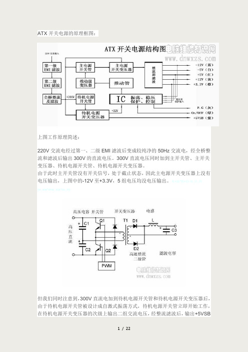
ATX开关电源的原理框图:上图工作原理简述:220V交流电经过第一、二级EMI滤波后变成较纯净的50Hz交流电,经全桥整流和滤波后输出300V的直流电压。
300V直流电压同时加到主开关管、主开关变压器、待机电源开关管、待机电源开关变压器。
由于此时主开关管没有开关信号,处于截止状态,因此主电源开关变压器上没有电压输出,上图中的-12V至+3.3V,5组电压均没电压输出。
电+脑*维+修-知.识_网(w_ww*dnw_xzs*co_m)但我们同时注意到,300V直流电加到待机电源开关管和待机电源开关变压器后,由于待机电源开关管被设计成自激式振荡方式,待机电源开关管立即开始工作,在待机电源开关变压器的次级上输出二组交流电压,经整流滤波后,输出+5VSB和+22V电压,+22V电压是专门为主控IC供电的。
+5VSB加到主板上作为待机电压。
当用户按动机箱的Power启动按键后,(绿)色线处于低电平,主控IC内部的振荡电路立即启动,产生脉冲信号,经推动管放大后,脉冲信号经推动变压器加到主开关管的基极,使主开关管工作在高频开关状态。
主开关变压器输出各组电压,经整流和滤波后得到各组直流电压,输出到主板。
但此时主板上的CPU仍未启动,必须等+5V的电压从零上升到95%后,IC检测到+5V上升到4.75V时,IC发出P.G信号,使CPU启动,电脑正常工作。
当用户关机时,绿色线处于高电平,IC内部立即停止振荡,主开关管因没有脉冲信号而停止工作。
-12至+3.3的各组电压降至为零。
电源处于待机状态。
输出电压的稳定则是依赖对脉冲宽度的改变来实现,这就叫做脉宽调制PWM。
由高压直流到低压多路直流的这一过程也可称DC-DC变换,是开关电源的核心技术。
采用开关变换的显著优点是大大提高了电能的转换效率,典型的PC电源效率为70—75%,而相应的线性稳压电源的效率仅有50%左右。
保护电路的工作原理:在正常使用过程中,当IC检测到负载处于:短路、过流、过压、欠压、过载等状态时,IC内部发出信号,使内部的振荡停止,主开关管因没有脉冲信而停止工作。
常见几种开关电源工作原理及电路图
开关式稳压电源接控制方式分为调宽式和调频式两种,在实际的应用中,调宽式使用得较多,在目前开发和使用的开关电源集成电路中,绝大多数也为脉宽调制型。
因此下面就主要介绍调宽式开关稳压电源。
调宽式开关稳压电源的基本原理可参见下图。
对于单极性矩形脉冲来说,其直流平均电压Uo取决于矩形脉冲的宽度,脉冲越宽,其直流平均电压值就越高。
直流平均电压U。
可由公式计算,即Uo=Um×T1/T式中Um为矩形脉冲最大电压值;T为矩形脉冲周期;T1为矩形脉冲宽度。
从上式可以看出,当Um 与T 不变时,直流平均电压Uo 将与脉冲宽度T1 成正比。
这样,只要我们设法使脉冲宽度随稳压电源输出电压的增高而变窄,就可以达到稳定电压的目的。
二、开关式稳压电源的原理电路1、基本电路图二开关电源基本电路框图开关式稳压电源的基本电路框图如图二所示。
交流电压经整流电路及滤波电路整流滤波后,变成含有一定脉动成份的直流电压,该电压进人高频变换器被转换成所需电压值的方波,最后再将这个方波电压经整流滤波变为所需要的直流电压。
控制电路为一脉冲宽度调制器,它主要由取样器、比较器、振荡器、脉宽调制及基准电压等电路构成。
这部分电路目前已集成化,制成了各种开关电源用集成电路。
控制电路用来调整高频开关元件的开关时间比例,以达到稳定输出电压的目的。
2.单端反激式开关电源单端反激式开关电源的典型电路如图三所示。
电路中所谓的单端是指高频变换器的磁芯仅工作在磁滞回线的一侧。
所谓的反激,是指当开关管VT1 导通时,高频变压器T初级绕组的感应电压为上正下负,整流二极管VD1处于截止状态,在初级绕组中储存能量。
当开关管VT1截止时,变压器T初级绕组中存储的能量,通过次级绕组及VD1 整流和电容C滤波后向负载输出。
单端反激式开关电源是一种成本最低的电源电路,输出功率为20-100W,可以同时输出不同的电压,且有较好的电压调整率。
唯一的缺点是输出的纹波电压较大,外特性差,适用于相对固定的负载。
大功率可调开关电源的电路图原理

大功率可调开关电源的电路图原理本文给出了一种新型大功率可调开关电源的设计方案。
采用Buck型开关电源拓扑,以带单路PWM输出和电流电压反馈检测MC33060为控制IC,配以双路输出IR2110驱动芯片,设计了一种可调高电压大功率的开关电源,有效解决了普通开关电源在非隔离拓扑结构下输出电压和功率不能达到很高的限制,并带有过流保护等电路。
文中以MC33060的应用为基础介绍了可调开关电源设计的方法,然后详细讲解了本系统的组成以及各个部分的作用,文章最后总结了该系统的特点。
1.引言开关电源作为线性稳压电源的一种替代物出现,其应用与实现日益成熟。
而集成化技术使电子设备向小型化、智能化方向发展,新型电子设备要求开关电源有更小的体积和更低的噪声干扰,以便实现集成一体化。
对中小功率开关电源来说是实现单片集成化,但在大功率应用领域,因其功率损耗过大,很难做成单片集成,不得不根据其拓扑结构在保证电源各项参数的同时尽量缩小系统体积。
2.典型开关电源设计开关电源一般由脉冲宽度调制(PWM,Pulse Width Modulation控制IC(Integrated Circuit和功率器件(功率MOSFET或IGBT构成,且符合三个条件:开关(器件工作在开关非线性状态、高频(器件工作在高频非接近上频的低频和直流(电源输出是直流而不是交流。
2.1控制IC以MC33060为例介绍控制IC。
MC33060是由安森美(ON Semi半导体公司生产的一种性能优良的电压驱动型脉宽调制器件,采用固定频率的单端输出,能工作在-40℃至85℃。
其内部结构如图1所示[1],主要特征如下:1集成了全部的脉宽调制电路;2内置线性锯齿波振荡器,外置元件仅一个电阻一个电容;3内置误差放大器;4内置5V参考电压,1.5%的精度;5可调整死区控制;6内置晶体管提供200mA的驱动能力;7欠压锁定保护;图1MC33060内部结构图其工作原理简述:MC33060是一个固定频率的脉冲宽度调制电路,内置线性锯齿波振荡器,振荡频率可通过外部的一个电阻和一个电容进行调节,其振荡频率如(2-1式:输出脉冲的宽度是通过电容CT上的正极性锯齿波电压与另外两个控制信号进行比较来实现。
开关电源电路详解图
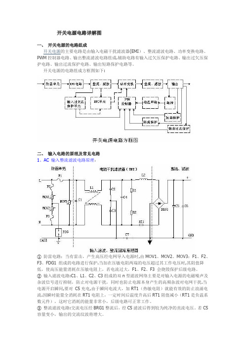
开关电源电路详解图一、开关电源的电路组成开关电源的主要电路是由输入电磁干扰滤波器(EMI)、整流滤波电路、功率变换电路、PWM控制器电路、输出整流滤波电路组成.辅助电路有输入过欠压保护电路、输出过欠压保护电路、输出过流保护电路、输出短路保护电路等。
开关电源的电路组成方框图如下:二、输入电路的原理及常见电路1、AC 输入整流滤波电路原理:①防雷电路:当有雷击,产生高压经电网导入电源时,由MOV1、MOV2、MOV3:F1、F2、F3、FDG1 组成的电路进行保护.当加在压敏电阻两端的电压超过其工作电压时,其阻值降低,使高压能量消耗在压敏电阻上,若电流过大,F1、F2、F3 会烧毁保护后级电路。
②输入滤波电路:C1、L1、C2、C3组成的双π型滤波网络主要是对输入电源的电磁噪声及杂波信号进行抑制,防止对电源干扰,同时也防止电源本身产生的高频杂波对电网干扰.当电源开启瞬间,要对C5充电,由于瞬间电流大,加RT1(热敏电阻)就能有效的防止浪涌电流.因瞬时能量全消耗在RT1电阻上,一定时间后温度升高后RT1阻值减小(RT1是负温系数元件),这时它消耗的能量非常小,后级电路可正常工作。
③整流滤波电路:交流电压经BRG1整流后,经C5滤波后得到较为纯净的直流电压。
若C5容量变小,输出的交流纹波将增大。
2、DC 输入滤波电路原理:①输入滤波电路:C1、L1、C2组成的双π型滤波网络主要是对输入电源的电磁噪声及杂波信号进行抑制,防止对电源干扰,同时也防止电源本身产生的高频杂波对电网干扰.C3、C4 为安规电容,L2、L3为差模电感。
② R1、R2、R3、Z1、C6、Q1、Z2、R4、R5、Q2、RT1、C7组成抗浪涌电路。
在起机的瞬间,由于C6的存在Q2不导通,电流经RT1构成回路.当C6上的电压充至Z1的稳压值时Q2导通.如果C8漏电或后级电路短路现象,在起机的瞬间电流在RT1上产生的压降增大,Q1导通使Q2没有栅极电压不导通,RT1将会在很短的时间烧毁,以保护后级电路。