基于单片机的多点温度检测系统的设计.外文翻译
基于单片机的多功能温度检测系统的设计翻译
基于单片机的多功能温度检测系统的设计一、引言随着社会的发展和技术的进步,人们越来越注重温度检测与显示的重要性。
温度检测与状态显示技术与设备已经普遍应用于各行各业,市场上的产品层出不穷。
温度检测及显示也逐渐采用自动化控制技术来实现监控。
本课题就是一个温度检测及状态显示的监控系统。
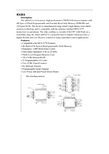
二、系统方案本系统采用AT89S52 作为该系统的单片机。
系统整体硬件电路包括,电源电路,传感器电路,温度显示电路,上下限报警电路等如图1 所示。
图中报警电路可以在被测温度不在上下限X围内时,发出报警鸣叫声音。
温度控制的基本原理为:当DSl8B20 采集到温度信号后,将温度信号送至AT89S52 中处理,同时将温度送到LCD 液晶屏显示,单片机根据初始化设置的温度上下限进行判断处理,即如果温度大于所设的最高温度就启动风扇降温;如果温度小于所设定的最低温度就启动报警装置。
温度控制器的原理图二三、系统硬件设计1.单片机AT89S52 的介绍AT89S52 是一种低功耗、高性能CMOS8 位微控制器,具有8K 可编Flash 存储器。
使用Atmel 公司高密度非易失性存储器技术制造,与工业80C51 产品指令和引脚完全兼容。
片上Flash 允许程序存储器在系统编程,亦适于常规编程器。
在单芯片上,拥有灵巧的8 位CPU和在系统可编程Flash,使AT89S52 为众多嵌入式控制应用系统提供高灵活、超有效的解决方案[5]。
AT89S52 具有以下标准功能:8k 字节Flash,256 字节RAM,32 位I/O 口线,看门狗定时器,2 个数据指针,三个16 位定时器/计数器,一个6 向量2 级中断结构,全双工串行口,片内晶振及时钟电路。
另外,AT89S52 可降至0Hz 静态逻辑操作,支持2 种软件可选择节电模式。
空闲模式下,CPU 停止工作,允许RAM、定时器/计数器、串口、中断继续工作。
掉电保护方式下,RAM 内容被保存,振荡器被冻结,单片机一切工作停止,直到下一个中断或硬件复位为止。
基于单片机的实时温度监控系统设计外文翻译毕业设计论文
安徽建筑工业学院毕业设计 (论文)专业电气工程及其自动化班级 07电气(1)课题基于单片机的实时温度监控系统设计基于单片机的实时温度监控系统设计摘要本文所介绍的是一种采用单总线数字式的温度传感器DS18B20与AT89S52单片机组成的新型温度测量系统,并使用LED数码管显示器将所测温度显示出来。
该系统以 AT89S52单片机为控制核心,利用新型一线制温度传感器 DS18B20测量温度值,实现环境温度的检测和报警。
系统测温范围为-40℃—+85℃,测量精度为 0.5℃。
用户可以自定义报警上、下限,一旦温度超过极限值,单片机便启动声光报警系统。
该系统精度高、测温范围广、报警及时,可广泛应用于基于单片机的温报警场合。
关键词:AT89S52单片机;温度测量;DS18B20;声光报警;数码管显示Design of Real-time Temperature Monitoring System Based on Single Chip MicrocomputerAbstractDescribed in this paper is a single-bus digital temperature sensor DS18B20 AT89S52 single chip with a new temperature measuring system,and use the LED digital display will display the measured temperature. The AT89S52 microcontroller for the control system to the core,Temperature sensor system using a new first-line temperature measurement DS18B20,achieve environmental temperature detection and alarm. Temperature measurement range is -40 ℃ - +85 ℃, measurement ac curacy of 0.5 ℃. Users can customize the alarm, the lower limit,Once the temperature exceeds the limit, the microcontroller will start the sound and light alarm system. The system of high precision, wide temperature range, the alarm in time, can be widely used in microcontroller-based temperature alarm occasions.Key words: AT89S52 microcontroller; temperature measurement; DS18B20; sound and light alarms; digital display目录摘要 (2)Abstract (3)目录 (4)第一章前言 (5)第二章监控系统主要元器件简介 (6)2.1 AT89S52单片机的组成结构及功能 (6)2.1 .1 AT89S52单片机的主要功能 (6)2.1.2 AT89S5单片机的封装及其引脚功能说明 (7)2.1.3外接晶振或外部振荡器引脚 (9)2.1.4 AT89S52复位 (9)2.2温度测量传感器DS18B20介绍 (10)2.2.1 DS18B20简介 (10)2.2.2 DS18B20的引脚、封装和结构 (10)2.2.3 寄生电源 (12)2.2.4 温度测量原理 (12)2.3 四位连体数码管SM410564 (13)第三章系统硬件电路设计 (15)3.1 单片机最小系统 (15)3.2 温度检测模块 (17)3.3 温度显示模块电路 (17)3.4报警电路模块 (17)3.5 基于AT89S52单片机的温度测量系统总电路 (18)3.6 温度测量系统的实物图 (19)第四章控制系统软件设计 (21)4.1 主程序 (21)4.2 子程序 (22)4.2.1读出温度子程序 (22)4.2.2温度转换命令子程序 (22)4.2.3计算温度子程序 (23)4.2.4显示数据刷新子程序 (24)第五章结论 (25)参考文献 (26)致谢 (27)附录一英文文献 (28)附录二中文翻译 (37)第一章前言温度是一种最基本的环境参数,对于我们来说,不仅仅是一个量的反映,更能直接影响作用到我们的生活中,人民的生活与环境的温度息息相关,在工业生产过程中需要实时测量温度,在农业生产中也离不开温度的测量。
基于单片机的温度检测与控制器的设计外文翻译 (1)
VTP ,所有的检测放大器晶体管(M1,M2,M3和M4)都偏向于饱和模式。
M1和M3(M2和M4)的栅源电压几乎是相同的,因为相同的电流流过每一个分支。
当PASE 变低时,左右位线具有相同的电位,21V V +。
由于位线电压相同,位线负载(CELL L I I +)和电容(BL I )的电流也相等。
由于存储单元细胞获取电流{CELL I ),成数量的电流(CELL I )在右边流动,以保持位线电压是相等的。
因此,目前DL 和DL 线之间出现了差异。
位线负载电容的传感速度几乎是独立的,因为BL 和BL 没有电容放电操作。
因此,BL 和BL 不需要预充电和均衡操作,从而导致速度和周期时间的损失。
图10.39所示电路的开环增益表示为 )2(*)1()4(*)3(m gm m gm m gm m gm Gain loop open =-gm(m1),gm(m2),gm(m3)和gm(m4)是M1,M2,M3和M4,分别。
电流检测放大器的一个缺点是大于电压检测放大器的功耗。
“这些放大器通常用于在高速SRAM 和高密度比如由于数据线的大负载电容256 MB DRAM (IO BL _和IOB BL _如图.10.15)。
14.4 非易失性存储器如DRAM 和SRAM 的MOS 内存结构的缺点是,在没有电源的情况下导致的数据丢失。
为了克服这个问题,各种非易失性和可编程(除掩模ROM )内存已提出。
最近,快闪记忆体的基础上浮动门的概念已成为最流行的非易失性存储器,由于其小单元尺寸和更好的功能。
因此,我们将详细描述的基本结构和操作掩模ROM 和在本节中的快闪记忆体。
只读存储器阵列,也可以被看作是一个简单的组合的布尔网络为每个输入组合,即产生一个指定的输出值,每个地址。
因此,存储在一个特定的地址位置的二进制信息可实现了从选定行(字线)选定的列(位线),这是等价的存在或缺乏设备在特定的位置。
在下面,我们将研究两个不同实现的MOS ROM 的阵列。
基于单片机的无线温度检测器的设计
ANYANG INSTITUTE OF TECHNOLOGY本科毕业论文基于单片机的无线温度检测器的设计The Design of Wireless Temperature Detector Based on MCU院(部)名称:电子信息与电气工程学院专业班级:自动化2009级2班学生姓名:******学号:200902020005指导教师姓名:******指导教师职称:讲师2013年5月毕业设计(论文)原创性声明和使用授权说明原创性声明本人郑重承诺:所呈交的毕业设计(论文),是我个人在指导教师的指导下进行的研究工作及取得的成果。
尽我所知,除文中特别加以标注和致谢的地方外,不包含其他人或组织已经发表或公布过的研究成果,也不包含我为获得安阳工学院及其它教育机构的学位或学历而使用过的材料。
对本研究提供过帮助和做出过贡献的个人或集体,均已在文中作了明确的说明并表示了谢意。
作者签名:日期:指导教师签名:日期:使用授权说明本人完全了解安阳工学院关于收集、保存、使用毕业设计(论文)的规定,即:按照学校要求提交毕业设计(论文)的印刷本和电子版本;学校有权保存毕业设计(论文)的印刷本和电子版,并提供目录检索与阅览服务;学校可以采用影印、缩印、数字化或其它复制手段保存论文;在不以赢利为目的前提下,学校可以公布论文的部分或全部内容。
作者签名:日期:目录摘要 (Ⅰ)Abstract (Ⅱ)第一章绪论 (1)1.1课题的背景和意义 (1)1.2本课题的研究内容以及所完成的工作 (1)1.2.1 本课题的研究内容 (1)1.2.2 本课题所完成的具体工作 (2)第二章无线温度检测系统总体设计 (3)2.1系统设计要求 (3)2.2系统总体设计方案的确定 (3)2.2.1 数字温度传感器的选择 (3)2.2.2 控制器的选择 (4)2.2.3 无线收发模块的选择 (5)第三章硬件电路设计 (7)3.1发射端 (7)3.1.1 温度采集模块 (7)3.1.2 控制单元STC89C52单片机 (9)3.1.3 电源模块设计 (12)3.1.4 无线收发模块NRF24L01电路设计 (12)3.1.5 时钟振荡电路设计 (13)3.1.6 复位电路设计 (13)3.2接收端 (14)3.2.1 蜂鸣器报警模块设计 (14)3.2.2 键盘电路设计 (15)3.2.3 液晶显示模块设计 (15)第四章软件程序设计 (18)4.1程序流程图 (18)4.1.1 主程序流程图 (18)4.1.2 子程序流程图 (19)4.2无线收发模块24L01的编程 (21)4.2.1 24L01编程的基本思路 (21)4.2.3 函数介绍 (22)4.3软件编译与调试 (23)4.3.1 程序设计语言的选用 (23)4.3.2 KeilC51简介 (24)4.3.3 uVision4集成开发环境 (24)4.3.4 软件调试与结果 (25)第五章安装与调试 (26)5.1 Altium Designer软件 (26)5.2电路板安装与调试 (26)结论 (27)致谢 (28)参考文献 (29)附录A元件清单 (30)附录B发射板原理图 (31)附录C接收板原理图 (32)附录D发射板实物图 (33)附录E接收板实物图 (34)附录F发射板源程序 (35)附录G接收板源程序 (44)基于单片机的无线温度检测器的设计摘要:无线温度检测器是一种用于仓库和蔬菜大棚等具有温度检测、无线传输、温度显示和超限报警功能的仪器。
基于单片机的多点温度测量系统设计

理工科类大学毕业设计论文南开大学本科生毕业设计中文题目:基于单片机的多点温度测量系统设计英文题目:Design of based on the microprocessor multipoint temperature measurement system学号:****姓名:****年级:****专业:电子信息科学与技术系别:电子科学系指导教师:****完成日期:****摘要通过运用DS18B20数字温度传感器的测温原理和特性,利用它独特的单线总线接口方式,与AT89C51单片机相结合实现多点测温。
并给出了测温系统中对DS18B20操作的C51编程实例。
实现了系统接口简单、精度高、抗干扰能力强、工作稳定等特点。
本文介绍基于AT89C51单片机、C语言和DS18B20传感器的多点温度测量系统设计及其在Proteus平台下的仿真。
利用51单片机的并行口,同步快速读取8支DS18B20温度,实现了在多点温度测量系统中对多个传感器的快速精确识别和处理,并给出了具体的编程实例和仿真结果。
关键词:单片机;DS18B20数字温度传感器;Proteus仿真;C51编程AbstractWith using the measuring principle and characteristics of the numerical temperature sensor of DS18B20,making use of special characteristics of single line as the total line, and combine together with AT89C51 to realize several points temperature measuring. Also this paper gives the example of the C51 program which is used to operate to the DS18B20. Make system have characteristics of simple, high accuracy, strong anti- interference ability, stable work etc.This design introduced AT89C51 monolithic integrated circuit temperature control system design from the hardware and the software two aspects. A multipoint temperature measurement system based on DS18B20 and AT89C51 microcontroller is designed and simulated by Proteus in this paper, including software and hardware design of this system. The system has such advantages as novel circuit design, quick measurement speed, high measurement accuracy, and good practicality.Key words: SCM;DS18B20;Proteus simulation;C51 program目录摘要 (I)Abstract ............................................................................................... I I 第一章绪论 (1)1.1温度智能测控系统的研究背景与现状分析 (1)1.2温度智能测控系统的工作原理 (2)第二章单片机简介 (3)2.1单片机的定义 (3)2.2单片机的基本结构 (4)2.3单片机执行指令的过程 (5)2.4单片机的特点 (6)第三章数字温度传感器DS18B20原理 (7)3.1概述 (7)3.2主要特征 (7)3.3引脚功能 (8)3.4工作原理及应用 (8)3.5单片机对DS18B20的操作流程 (8)3.6 DS18B20与单片机的接口 (9)3.7 DS18B20芯片ROM指令表 (9)3.8 DS18B20芯片存储器操作指令表 (10)3.9 DS18B20复位及应答关系及读写隙 (11)第四章系统硬件设计 (12)4.1系统结构设计思路 (12)4.2系统框图 (13)4.3系统硬件设计 (13)第五章系统软件设计 (16)5.1 系统软件设计思路 (16)5.2系统软件设计 (21)第六章系统运行结果 (27)第七章结束语 (31)参考文献 (32)致谢 (33)第一章绪论1.1温度智能测控系统的研究背景与现状分析温度是一个和人们生活环境有着密切关系的物理量,也是一种在生产、科研、生活中需要测量和控制的重要物理量,是国际单位制七个基本量之一,同时它也是一种最基本的环境参数。
单片机温度探测系统中英文对照外文翻译文献

中英文对照翻译附件1:外文资料翻译译文一种基于DS18B20的温度探测系统摘要所有的DS18B20传感器,用于多点温度测试,IO总线与MCU连接,温度数据的轮流收集。
如果系统有大量的传感器,MCU的时间用在处理温度数据明显延长,因此周期替代测试变得更长。
在本文中,一种新的方法,DS18B20的合理组合和一些在软件上采取的措施,替代试验进展速度明显。
关键词:DS18B20的集团,温度测试,轮流测试所花费的时间。
引言由于结构简单,安装方便,低损失和广泛的用途的温度测试,DS18B20温度测试传感器应用领域,需要多点温度测试,如化学工业,粮食,环境监督管理等。
因为通过一个DS18B20的多点温度测试系统总线,所有DS18B20是挂在一条总线上,然后每个温度测试点的值转换轮流读。
作为转换后读值必须阅读8次引脚的状态,移动时间,位置和存储数据,所以时间多花费在阅读每一个点的数据系统时间。
如果温度测试系统是大型系统由它造成的损失是相当多的,然后交替测试系统的运行速度明显降低,从而影响多点温度测试系统的效率。
在本文中,DS18B20的一些I / O总线上都挂着分组DS18B20的均匀,温度转换获取数据读取DS18B20的状态,系统损耗减少和替代测试速度增加显然,这将不会影响精度和转换的可靠性。
一套点对多点温度,在此实现人工环境实验室测试,这增加了测试效率。
作者对DS18B20的认识DS18B20是单总线数字温度传感器来自美国达拉斯公司。
DS18B20是由64数字光盘刻激光,温度敏感性组成部分,非易失性温度报警触发器(设备TH和TL)。
DS18B20的通信微处理器单总线端口和测试范围DS18B20是从-55摄氏度到+125摄氏度,增量值是0.5摄氏度。
温度可在720ms的数字改为每个DS18B20具有唯一的64数字序号。
图1揭示的具体内容:两个8的数字储量(0号和1号),用于存储在DS18B20的温度值。
0号存储存储器温度值,补充和一号存储器温度值的符号。
单片机温度控制系统外文翻译外文文献英文文献中英翻译

Design of the Temperature Control System Based onAT89C51ABSTRACTThe principle and functions of the temperature control system based on micro controller AT89C51 are studied, and the temperature measurement unit consists of the 1-Wire bus digital temperature sensor DS18B20. The system can be expected to detect the preset temperature, display time and save monitoring data. An alarm will be given by system if the temperature exceeds the upper and lower limit value of the temperature which can be set discretionarily and then automatic control is achieved, thus the temperature is achieved monitoring intelligently within a certain range. Basing on principle of the system, it is easy to make a variety of other non-linear control systems so long as the software design is reasonably changed. The system has been proved to be accurate, reliable and satisfied through field practice.KEYWORDS: AT89C51; micro controller; DS18B20; temperature 1 INTRODUCTIONTemperature is a very important parameter in human life. In the modern society, temperature control (TC) is not only used in industrial production, but also widely used in other fields. With the improvement of the life quality, we can find the TC appliance in hotels, factories and home as well. And the trend that TC will better serve the whole society, so it is of great significance to measure and control the temperature. Based on the AT89C51 and temperature sensor DS18B20, this system controls the condition temperature intelligently. The temperature can be set discretionarily within a certain range. The system can show the time on LCD, and save monitoring data; andautomatically control the temperature when the condition temperature exceeds the upper and lower limit value. By doing so it is to keep the temperature unchanged. The system is of high anti-jamming, high control precision and flexible design; it also fits the rugged environment. It is mainly used in people's life to improve the quality of the work and life. It is also versatile, so that it can be convenient to extend the use of the system. So the design is of profound importance. The general design, hardware design and software design of the system are covered.1.1 IntroductionThe 8-bit AT89C51 CHMOS microcontrollers are designed to handle high-speed calculations and fast input/output operations. MCS 51 microcontrollers are typically used for high-speed event control systems. Commercial applications include modems, motor-control systems, printers, photocopiers, air conditioner control systems, disk drives, and medical instruments. The automotive industry use MCS 51 microcontrollers in engine-control systems, airbags, suspension systems, and antilock braking systems (ABS). The AT89C51 is especially well suited to applications that benefit from its processing speed and enhanced on-chip peripheral functions set, such as automotive power-train control, vehicle dynamic suspension, antilock braking, and stability control applications. Because of these critical applications, the market requires a reliable cost-effective controller with a low interrupt latency response, ability to service the high number of time and event driven integrated peripherals needed in real time applications, and a CPU with above average processing power in a single package. The financial and legal risk of having devices that operate unpredictably is very high. Once in the market, particularly in mission critical applications such as an autopilot or anti-lock braking system, mistakesare financially prohibitive. Redesign costs can run as high as a $500K, much more if the fix means 2 back annotating it across a product family that share the same core and/or peripheral design flaw. In addition, field replacements of components is extremely expensive, as the devices are typically sealed in modules with a total value several times that of the component. To mitigate these problems, it is essential that comprehensive testing of the controllers be carried out at both the component level and system level under worst case environmental and voltage conditions. This complete and thorough validation necessitates not only a well-defined process but also a proper environment and tools to facilitate and execute the mission successfully. Intel Chandler Platform Engineering group provides post silicon system validation (SV) of various micro-controllers and processors. The system validation process can be broken into three major parts. The type of the device and its application requirements determine which types of testing are performed on the device.1.2 The AT89C51 provides the following standard features4Kbytes of Flash, 128 bytes of RAM, 32 I/O lines, two 16-bittimer/counters, a five vector two-level interrupt architecture, a full duple ser-ial port, on-chip oscillator and clock circuitry. In addition, the AT89C51 is designed with static logic for operation down to zero frequency and supports two software selectable power saving modes. The Idle Mode stops the CPU while allowing the RAM, timer/counters, serial port and interrupt sys -tem to continue functioning. The Power-down Mode saves the RAM contents but freezes the oscil–lator disabling all other chip functions until the next hardware reset.1.3Pin DescriptionVCC Supply voltage.GND Ground.Port 0:Port 0 is an 8-bit open-drain bi-directional I/O port. As an output port, each pin can sink eight TTL inputs. When 1s are written to port 0 pins, the pins can be used as high impedance inputs. Port 0 may also be configured to be the multiplexed low order address/data bus during accesses to external program and data memory. In this mode P0 has internal pull ups. Port 0 also receives the code bytes during Flash programming, and outputs the code bytes during program verification. External pull ups are required during program verification.Port 1:Port 1 is an 8-bit bi-directional I/O port with internal pull ups. The Port 1 output buffers can sink/so -urce four TTL inputs. When 1s are written to Port 1 pins they are pulled high by the internal pull ups and can be used as inputs. As inputs, Port 1 pins that are externally being pulled low will source current (IIL) because of the internal pullups. Port 1 also receives the low-order address bytes during Flash programming and verification.Port 2:Port 2 is an 8-bit bi-directional I/O port with internal pull ups. The Port 2 output buffers can sink/source four TTL inputs. When 1s are written to Port 2 pins they are pulled high by the internal pull ups and can be used as inputs. As inputs, Port 2 pins that are externally being pulled low will source current (IIL) because of the internal pull ups. Port 2 emits the high-order address byte during fetches from external program memory and during accesses to Port 2 pins that are externally being pulled low will source current (IIL) because of the internal pull ups. Port 2 emits the high-order address byte during fetches from external program memory and during accesses to external data memory that use 16-bit addresses (MOVX@DPTR). In this application,it uses strong internal pull-ups when emitting 1s. During accesses to external data memory that use 8-bit addresses (MOVX @ RI), Port 2 emits the contents of the P2 Special Function Register. Port 2 also receives the high-order address bits and some control signals durin Flash programming and verification.Port 3:Port 3 is an 8-bit bi-directional I/O port with internal pull ups. The Port 3 output buffers can sink/sou -rce four TTL inputs. When 1s are written to Port 3 pins they are pulled high by the internal pull ups and can be used as inputs. As inputs, Port 3 pins that are externally being pulled low will source current (IIL) because of the pull ups.Port 3 also serves the functions of various special features of the AT89C51 as listed below:RST:Reset input. A high on this pin for two machine cycles while the oscillator is running resets the device.ALE/PROG:Address Latch Enable output pulse for latching the low byte of the address during accesses to external memory. This pin is also the program pulse input (PROG) during Flash programming. In normal operation ALE is emitted at a constant rate of 1/6 the oscillator frequency, and may be used for external timing or clocking purposes. Note, however, that one ALE pulse is skipped duri-ng each access to external Data Memory. If desired, ALE operation can be disabled by setting bit 0 of SFR location 8EH. With the bit set, ALE is active only during a MOVX or MOVC instruction. Otherwise, the pin is weakly pulled high. Setting the ALE-disable bit has no effect if the microcontroller is in external execution mode.PSEN:Program Store Enable is the read strobe to external program memory. When theAT89C51 is executing code from external program memory, PSEN is activated twice each machine cycle, except that two PSEN activations are skippedduring each access to external data memory.EA/VPP:External Access Enable. EA must be strapped to GND in order to enable the device to fetch code from external program memory locations starting at 0000H up to FFFFH. Note, however, that if lock bit 1 is programmed, EA will be internally latched on reset. EA should be strapped to VCC for internal program executions. This pin alsreceives the 12-volt programming enable voltage (VPP) during Flash programming, for parts that require 12-volt VPP.XTAL1:Input to the inverting oscillator amplifier and input to the internal clock operating circuit.XTAL2 :Output from the inverting oscillator amplifier. Oscillator CharacteristicsXTAL1 and XTAL2 are the input and output, respectively, of an inverting amplifier which can be configured for use as an on-chip oscillator, as shown in Figure 1. Either a quartz crystal or ceramic resonator may be used. To drive the device from an external clock source, XTAL2 should be left unconnected while XTAL1 is driven as shown in Figure 2.There are no requirements on the duty cycle of the external clock signal, since the input to the internal clocking circuitry is through a divide-by-two flip-flop, but minimum and maximum voltage high and low time specifications must be observed. Idle Mode In idle mode, the CPU puts itself to sleep while all the on chip peripherals remain active. The mode is invoked by software. The content of the on-chip RAM and all the special functions registers remain unchanged during this mode. The idle mode can be terminated by any enabled interrupt or by a hardware reset. It should be noted that when idle is terminated by a hard ware reset, the device normally resumes program execution, from where it left off, up to two machine cycles before the internal reset algorithm takes control. On-chip hardware inhibits accessto internal RAM in this event, but access to the port pins is not inhibited. To eliminate the possibility of an unexpected write to a port pin when Idle is terminated by reset, the instruction following the one that invokes Idle should not be one that writes to a port pin or to external memory.Power-down ModeIn the power-down mode, the oscillator is stopped, and the instruction that invokes power-down is the last instruction executed. The on-chip RAM and Special Function Registers retain their values until the power-down mode is terminated. The only exit from power-down is a hardware reset. Reset redefines the SFRS but does not change the on-chip RAM. The reset should not be activated before VCC is restored to its normal operating level and must be held active long enough to allow the oscillator to restart and stabilize. The AT89C51 code memory array is programmed byte-by byte in either programming mode. To program any nonblank byte in the on-chip Flash Memory, the entire memory must be erased using the Chip Erase Mode.2 Programming AlgorithmBefore programming the AT89C51, the address, data and control signals should be set up according to the Flash programming mode table and Figure 3 and Figure 4. To program the AT89C51, take the following steps.1. Input the desired memory location on the address lines.2. Input the appropriate data byte on the data lines. 3. Activate the correct combination of control signals. 4. Raise EA/VPP to 12V for the high-voltage programming mode. 5. Pulse ALE/PROG once to program a byte in the Flash array or the lock bits. The byte-write cycle is self-timed and typically takes no more than 1.5 ms. Repeat steps 1 through 5, changing the address and data for the entire array or until the end of the object reached. Data Polling: The AT89C51features Data Polling to indicate the end of a write cycle. During a write cycle, an attempted read of the last byte written will result in the complement of the written datum on PO.7. Once the write cycle has been completed, true data are valid on all outputs, and the next cycle may begin. Data Polling may begin any time after a write cycle has been initiated.2.1Ready/Busy:The progress of byte programming can also be monitored by the RDY/BSY output signal. P3.4 is pulled low after ALE goes high during programming to indicate BUSY. P3.4 is pulled high again when programming is done to indicate READY.Program Verify:If lock bits LB1 and LB2 have not been programmed, the programmed code data can be read back via the address and data lines for verification. The lock bits cannot be verified directly. Verification of the lock bits is achieved by observing that their features are enabled.2.2 Chip Erase:The entire Flash array is erased electrically by using the proper combination of control signals and by holding ALE/PROG low for 10 ms. The code array is written with all “1”s. The chip erase operation must be executed before the code memory can be re-programmed.2.3 Reading the Signature Bytes:The signature bytes are read by the same procedure as a normal verification of locations 030H, 031H, and 032H, except that P3.6 and P3.7 must be pulled to a logic low. The values returned areas follows.(030H) = 1EH indicates manufactured by Atmel(031H) = 51H indicates 89C51(032H) = FFH indicates 12V programming(032H) = 05H indicates 5V programming2.4 Programming InterfaceEvery code byte in the Flash array can be written and the entire array can be erased by using the appropriate combination of control signals. The write operation cycle is self timed and once initiated, will automatically time itself to completion. A microcomputer interface converts information between two forms. Outside the microcomputer the information handled by an electronic system exists as a physical signal, but within the program, it is represented numerically. The function of any interface can be broken down into a number of operations which modify the data in some way, so that the process of conversion between the external and internal forms is carried out in a number of steps. An analog-to-digital converter(ADC) is used to convert a continuously variable signal to a corresponding digital form which can take any one of a fixed number of possible binary values. If the output of the transducer does not vary continuously, no ADC is necessary. In this case the signal conditioning section must convert the incoming signal to a form which can be connected directly to the next part of the interface, the input/output section of the microcomputer itself. Output interfaces take a similar form, the obvious difference being that here the flow of information is in the opposite direction; it is passed from the program to the outside world. In this case the program may call an output subroutine which supervises the operation of the interface and performs the scaling numbers which may be needed for digital-to-analog converter(DAC). This subroutine passes information in turn to an output device which produces a corresponding electrical signal, which could be converted into analog form using a DAC. Finally the signal is conditioned(usually amplified) to a form suitable for operating an actuator.The signals used within microcomputer circuits are almost always too small to be connected directly to the outside world” and some kind of interface must be used to translate them to a more appropriate form. The design of section of interface circuits is one of the most important tasks facing the engineer wishing to apply microcomputers. We have seen that in microcomputers information is represented as discrete patterns of bits; this digital form is most useful when the microcomputer is to be connected to equipment which can only be switched on or off, where each bit might represent the state of a switch or actuator. To solve real-world problems, a microcontroller must have more than just a CPU, a program, and a data memory. In addition, it must contain hardware allowing the CPU to access information from the outside world. Once the CPU gathers information and processes the data, it must also be able to effect change on some portion of the outside world. These hardware devices, called peripherals, are the CPU’s window to the outside.The most basic form of peripheral available on microcontrollers is the general purpose I70 port. Each of the I/O pins can be used as either an input or an output. The function of each pin is determined by setting or clearing corresponding bits in a corresponding data direction register during the initialization stage of a program. Each output pin may be driven to either a logic one or a logic zero by using CPU instructions to pin may be viewed (or read.) by the CPU using program instructions. Some type of serial unit is included on microcontrollers to allow the CPU to communicate bit-serially with external devices. Using a bit serial format instead of bit-parallel format requires fewer I/O pins to perform the communication function, which makes it less expensive, but slower. Serial transmissions are performed either synchronously orasynchronously.3 SYSTEM GENERAL DESIGNThe hardware block diagram of the TC is shown in Fig.1. The system hardware includes the micro controller, temperature detection circuit, keyboard control circuit, clock circuit, Display, alarm, drive circuit and external RAM. Based on the AT89C51, the DS18B20 will transfer the temperature signal detected to digital signal. And the signal is sent to the micro controller for processing. At last the temperature value is showed on the LCD 12232F. These steps are used to achieve the temperature detection. Using the keyboard interface chip HD7279 to set the temperature value, using the micro controller to keep a certain temperature, and using the LCD to show the preset value for controlling the temperature. In addition, the clock chip DS1302 is used to show time and the external RAM 6264 is used to save the monitoring data. An alarm will be given by buzzer in time if the temperature exceeds the upper and lower limit value of the temperature.3.1 HARDWARE DESIGNA. Micro controllerThe AT89C51 is a low-power, high-performance CMOS 8-bit micro controller with 4K bytes of in-system programmable Flash memory. The device is manufactured using At mel’s high-density nonvolatile memory technology and is compatible with the industry-standard 80C51 instruction set and pin out. The on-chip Flash allows the program memory to be reprogrammed in-system or by a conventional nonvolatile memory programmer. By combining a versatile 8-bit CPU with in-system programmable Flash on a monolithic chip, the At mel AT89C51 is a powerful micro controller which provides a highly-flexible and cost-effective solution to many embedded controlapplications. Minimum system of the micro controller is shown in Fig. 2. In order to save monitoring data, the 6264 is used as an external RAM. It is a static RAM chip, low-power with 8K bytes memory.B. Temperature Detection CircuitThe temperature sensor is the key part in the system. The Dallas DS18B20 is used, which supports the 1-Wire bus interface, and the ON-BOARD Patented is used internally. All the sensor parts and the converting circuit are integrated in integrated circuit like a transistor [1]. Its measure range is -55℃~125 ℃, and the precision between -10℃~85℃is ±0.5℃[2 ,3]. The temperature collected by the DS18B20 is transmitted in the 1-Wire bus way, and this highly raises the system anti-jamming and makes it fit in situ temperature measurement of the rugged environment [4]. There are two power supply ways for the DS18B20. The first is external power supply: the first pin of the DS18B20 is connected to the ground; the second pin serves as signal wire and the third is connected to the power. The second way is parasite power supply [5]. As the parasite power supply will lead to the complexity of the hardware circuit, the difficulty of the software control and the performance degradation of the chip, etc. But the DS18B20(s) can be connected to the I/O port of the micro controller in the external power supply way and it is more popular. Therefore the external power supply is used and the second pin is connected to the pin P1.3 of the AT89S51. Actually, if there are multipoint to be detected, the DS18B20(s) can be connected to the 1-Wire bus. But when the number is over 8, there is a concern to the driving and the more complex software design as well as the length of the 1-Wire bus. Normally it is no more than 50m. To achieve distant control, the system can be designed in to a wireless one to break the length limit of the 1-Wire bus [6].C. LCD CircuitThe LCD 12232F is used, which can be used to show characters, temperature value and time, and supply a friendly display interface. The 12232F is a LCD with 8192 128×32 pixels Chinese character database and 128 16×8 pixels ASCII character set graphics. It mainly consists of row drive/column drive and 128×32 full lattice LCD with t he function of displaying graphics as well as 7.5×2 Chinese characters. It is in a parallel or serial mode to connect to external CPU [7]. In order to economize the hardware resource, the 12232F should be connected to the AT89S51 in serial mode with only 4 output ports used. The LCD grayscale can be changed by adjusting the variable resistor connected the pin Vlcd of the LCD. CLK is used to transmit serial communication clock. SID is used to transmit serial data. CS is used to enable control the LCD. L+ is used to control the LCD backlight power.D. Clock CircuitThe Dallas DS18B20 is used, which is a high performance, low-power and real-time clock chip with RAM. The DS18B20 serves in the system with calendar clock and is used to monitor the time. The time data is read and processed by the AT89C51 and then displayed by the LCD. Also the time can be adjusted by the keyboard. The DS18B20 crystal oscillator is set at 32768Hz, and the recommended compensation capacitance is 6pF. The oscillator frequency is lower, so it might be possible not to connect the capacitor, and this would not make a big difference to the time precision. The backup power supply can be connected to a 3.6V rechargeable battery.E. Keyboard Control CircuitThe keyboard interface in the system is driven by the HD7279A which has a +5V single power supply and which is connected to the keyboard and display without using anyactive-device. According to the basic requirements and functions of the system, only 6 buttons are needed. The system's functions are set by the AT89C51 receiving the entered data. In order to save the external resistor, the 1×6 keyboard is used, and the keyboard codes are defined as: 07H, 0FH, 17H, 1FH, 27H, 2FH. The order can be read out by reading the code instruction. HD7279A is connected to the AT89S51 in serial mode and only 4 ports are need. As shown in Fig. 6, DIG0~DIG5 and DP are respectively the column lines and row line ports of the six keys which achieve keyboard monitoring, decoding and key codes identification.F. Alarm CircuitIn order to simplify the circuit and convenient debugging, a 5V automatic buzzer is used in the alarm circuit [8]. And this make the software programming simplified. As shown in Fig. 7, it is controlled by the PNP transistor 9012 whose base is connected to the pin P2.5 of the AT89C51. When the temperature exceeds the upper and lower limit value, the P2.5 output low level which makes the transistor be on and then an alarm is given by the buzzer.G. Drive CircuitA step motor is used as the drive device to control the temperature. The four-phase and eight-beat pulse distribution mode is used to drive motor and the simple delay program is used to handle the time interval between the pulses to obtain different rotational speed. There are two output states for the step motor. One: when the temperature is over the upper value, the motor rotates reversely (to low the temperature), while when lower than the lower limit value, the motor rotates normally (to raise the temperature); besides not equals the preset value. Two: when the temperature is at somewhere between the two endsand equals the preset value, the motor stops. These steps are used to achieve the temperature control. In addition, the motor speed can also be adjusted by relative buttons. As shown in Fig. 8, the code data is input through ports A11~A8 (be P2.3~P2.0) of the AT89C51 and inverted output by the inverter 74LS04. Finally it is amplified by the power amplifier 2803A to power the motor.3.2 SOFTWARE DESIGNAccording to the general design requirement and hardware circuit principle of the system, as well as the improvement of the program readability, transferability and the convenient debugging, the software design is modularized. The system flow mainly includes the following 8 steps: POST (Power-on self-test), system initiation, temperature detection, alarm handling, temperature control, clock chip DS18B20 operation, LCD and keyboard operation. The main program flow is shown in Fig. 9. Give a little analysis to the above 8 tasks, it is easy to find out that the last five tasks require the real time operation. But to the temperature detection it can be achieved with timer0 timing 1 second, that is to say temperature detection occurs per second. The system initiation includes global variable definition, RAM initiation, special function register initiation and peripheral equipment initiation. Global variable definition mainly finishes the interface definition of external interface chip connected to the AT89C51, and special definition of some memory units. RAM initiation mainly refers to RAM processing. For example when the system is electrified the time code will be stored in the internal unit address or the scintillation flag will be cleared. The special function register initiation includes loading the initial value of timer and opening the interrupt. For example, when the system is electrified the timer is initialized. Theperipheral equipment initiation refers to set the initial value of peripheral equipment. For example, when the system is electrified, the LCD should be initialized, the start-up display should be called, the temperature conversion command should be issued firstly and the clock chip DS18B20 should also be initialized. The alarm handling is mainly the lowering and the raising of temperature to make the temperature remain with the preset range. When the temperature is between the upper and the lower limit value, it goes to temperature control handling, that is to say the temperature need to be raised or lowered according to the preset value. By doing so make the condition temperature equal to the preset value and hence to reach the temperature target.4 CONCLUSIONThe temperature control system has the advantages of friendly human-computer interaction interface, simple hardware, low cost, high temperature control precision (error in the range of ±1 ℃), convenience and versatility, etc. It can be widely used in the occasions with -55℃to 125℃range, and there is a certain practical value.温度控制系统的设计摘要研究了基于AT89C51单片机温度控制系统的原理和功能,温度测量单元由单总线数字温度传感器DS18B20构成。
基于单片机的DS18B20多点测温系统LCD1602显示(完全免费)

河南科技学院HENANKEJIXUEYUAN毕业论文(设计)中文题目:基于单片机的DS18B20温度传感器测温系统设计英文题目:A Design of the DS18B20 Temperature Test System Based on MCU姓名牛鸿昌刘东学号201018033305专业班级应用电子技术指导教师赵小静提交日期2013年 5 月20 日教务处制基于单片机的DS18B20温度传感器测温系统设计姓名:** 班级:***指导老师:*** 职称:**(惠州学院电子科学系,广东,惠州,516007)摘要随着社会的进步和工业技术的发展,人们越来越重视温度因素,许多产品对温度范围要求严格,而目前市场上普遍存在的温度检测仪器大都是单点测量,同时有温度传递不及时、精度不够的缺点,不利于工业控制者根据温度变化及时作出决定。
在这样的形式下,开发一种能够同时测量多点,并且实时性高、精度高,能够综合处理多点温度信息的测量系统就很有必要。
本课题以AT89C52单片机系统为核心,能对多点温度进行实时巡检。
DS18B20是一种可组网的高精度数字式温度传感器,由于其具有单总线的独特优点,可以使用户轻松的组建起传感器网络,并可使多点温度测量电路变得简单、可靠。
本文结合实际使用经验,介绍了DS18B20数字温度传感器在单片机下的硬件连接及软件编程,并给出了软件流程图。
关键词:DS18B20 多点测温单片机LCD1602AbstractAs the industry and the society developing, the temperature becomes more and more important and a lot of products are sensitive to temperature. However, temperature measuring apparatus in the market now only can check and measure the temperature of one point, at the same time, the temperature information is not real time and the precision is low. It takes a great of troubles for the industry-controllers to make decision .In this situation, design and implement one applicable system which can watch measure and control the temperature and the measuring results is real time and the precision is great is more essential. In order to meeting this application, this paper talk about The Multiple-Point’s temperature Measuring System.This system based on single chip computer, can inspect and control multiple temperatures in real time. As a kind of high-accuracy digital net temperature sensor,DS18 B20 can be used building a sensor net easily. It can also make the net simple and reliable with it's special 1-wire interface .This paper introduces the application of DS18B20 with single chip processor.Key words:DS18B20 Multi-point temperature MCU LCD1602目录摘要 (II)Abstract ........................................................................................................................ I II 第一章绪论.. (1)1.1 课题背景 (1)1.2 本课题研究意义 (2)1.3 本课题的任务 (2)1.4 系统整体目标 (3)第二章方案论证比较与选择 (3)2.1 引言 (3)2.2 方案设计 (3)2.3 方案的比较与选择 (4)第三章硬件设计 (4)3.1 STC89C52单片机简介 (4)3.2 DS18B20介绍 (8)3.3 系统电路设计 (16)3.4 显示电路设计 (17)3.5 按键电路设计 (17)3.6 三点测温电路 (18)第四章软件设计 (18)4.1 软件开发工具的选择 (18)4.2 系统软件设计的一般原则 (19)4.3 系统软件设计的一般步骤 (20)4.4 三路测温软件实现 (20)第五章误差分析 (25)5.1 误差产生 (25)5.2 降低误差方法 (25)5.3 挂接DS18B20个数论证 (26)第六章调试与小结 (26)致谢 (28)参考文献 (29)附录 (30)第一章绪论1.1 课题背景在人类的生活环境中,温度扮演着极其重要的角色。
温度控制系统中英文对照外文翻译文献

温度控制系统中英文对照外文翻译文献温度控制系统中英文对照外文翻译文献温度控制系统中英文对照外文翻译文献(文档含英文原文和中文翻译)译文:温度控制系统的设计摘要:研究了基于AT89S 51单片机温度控制系统的原理和功能,温度测量单元由单总线数字温度传感器DS18B 20构成。
该系统可进行温度设定,时间显示和保存监测数据。
如果温度超过任意设置的上限和下限值,系统将报警并可以和自动控制的实现,从而达到温度监测智能一定范围内。
基于系统的原理,很容易使其他各种非线性控制系统,只要软件设计合理的改变。
该系统已被证明是准确的,可靠和满意通过现场实践。
践。
关键词:单片机;温度;温度关键词:单片机;温度;温度I. 导言温度是在人类生活中非常重要的参数。
在现代社会中,温度控制(TC TC)不仅用于工业生产,还广泛应用于其它领域。
随着生活质量的提)不仅用于工业生产,还广泛应用于其它领域。
随着生活质量的提高,我们可以发现在酒店,工厂和家庭,以及比赛设备。
而比赛的趋势将更好地服务于整个社会,因此它具有十分重要的意义测量和控制温度。
度。
在AT89S51AT89S51单片机和温度传感器单片机和温度传感器DS18B20DS18B20的基础上,系统环境的基础上,系统环境温度智能控制。
温度可设定在一定范围内动任意。
该系统可以显示在液晶显示屏的时间,并保存监测数据,并自动地控制温度,当环境温度超过上限和下限的值。
这样做是为了保持温度不变。
该系统具有很高的抗干扰能力,控制精度高,灵活的设计,它也非常适合这个恶劣的环境。
它主要应用于人们的生活,改善工作和生活质量。
这也是通用的,因此它可以方便地扩大使用该系统。
因此,设计具有深刻的重要性。
一般的设计,硬件设计和软件系统的设计都包括在内。
设计,硬件设计和软件系统的设计都包括在内。
II. 系统总体设计该系统硬件包括微控制器,温度检测电路,键盘控制电路,时钟电路,显示,报警,驱动电路和外部RAM RAM。
外文翻译--基于51单片机温度报警器的设计(适用于毕业论文外文翻译+中英文对照)

外文翻译--基于51单片机温度报警器的设计(适用于毕业论文外文翻译+中英文对照)XXX: Design of a Temperature Alarm Based on 51 MCUDepartment: n EngineeringMajor: Measurement and Control Technology and nClass:Student ID:Name:Supervisor:Date:A microcontroller。
also known as a single-chip computer system。
XXX its ns being integrated on a small chip。
it has most of the components needed for a complete computer system。
such as CPU。
memory。
internal and external bus systems。
and mostof them also have external storage。
At the same time。
it integrates XXX interfaces。
timers。
real-time clocks。
etc。
The most XXX integrate sound。
image。
ork。
and complex input-output systems on a single chip.XXX used in the industrial control field。
Microcontrollers XXX CPUs inside the chip。
The original design concept was to integrate a large number of peripheral devices and CPUs on a chip to make the computer system XXX's Z80 was the first processor designed according to this concept。
基于单片机的外文翻译、中英文翻译
英文原文DescriptionThe at89s52 is a low-power, high-performance CMOS 8-bit microcomputer with 4K bytes of Flash Programmable and Erasable Read Only Memory (PEROM) and 128 bytes RAM. The device is manufactured using Atmel’s high density nonvolatile memory technology and is compatible with the industry standard MCS-51™ instruction set and pinout. The chip combines a versatile 8-bit CPU with Flash on a monolithic chip, the Atmel at89s52 is a powerful microcomputer which provides a highly flexible and cost effective solution to many embedded control applications.Features:• Compatible with MCS-51™ Products• 4K Bytes of In-System Reprogrammable Flash Memory• Endurance: 1,000 Write/Erase Cycles• Fully Static Operation: 0 Hz to 24 MHz• Three-Level Program Memory Lock• 128 x 8-Bit Internal RAM• 32 Programmable I/O Lines• Two 16-Bit Timer/Counters• Six Interrupt Sources• Programmable Serial Channel• Low Power Idle and Power Down ModesThe at89s52 provides the following standard features: 4K bytes of Flash, 128 bytes of RAM, 32 I/O lines, two 16-bit timer/counters, a five vector two-level interrupt architecture, a full duplex serial port, on-chip oscillator and clock circuitry. In addition, the at89s52 is designed with static logic for operation down to zero frequency and supports two software selectable power saving modes. The Idle Mode stops the CPU while allowing the RAM, timer/counters, serial port and interrupt system to continue functioning. The Power Down Mode saves the RAM contents but freezes the oscillator disabling all other chip functions until the next hardware reset. Pin Description:VCC Supply voltage.GND Ground.Port 0Port 0 is an 8-bit open drain bidirectional I/O port. As an output port each pin can sink eight TTL inputs. When is are written to port 0 pins, the pins can be used as high impedance inputs.Port 0 may also be configured to be the multiplexed loworder address/data bus during accesses to external program and data memory. In this mode P0 has internal pullups.Port 0 also receives the code bytes during Flash programming, and outputs theduring accesses to external memory. This pin is also the program pulse input (PROG) during Flash programming.In normal operation ALE is emitted at a constant rate of 1/6 the oscillator frequency, and may be used for external timing or clocking purposes. Note, however, that one ALE pulse is skipped during each access to external Data Memory.If desired, ALE operation can be disabled by setting bit 0 of SFR location 8EH. With the bit set, ALE is active only during a MOVX or MOVC instruction. Otherwise, the pin is weakly pulled high. Setting the ALE-disable bit has no effect if the microcontroller is in external execution mode.PSENProgram Store Enable is the read strobe to external program memory.When the at89s52 is executing code from external program memory, PSEN is activated twice each machine cycle, except that two PSEN activations are skipped during each access to external data memory.EA/VPPExternal Access Enable. EA must be strapped to GND in order to enable the device to fetch code from external program memory locations starting at 0000H up to FFFFH. Note, however, that if lock bit 1 is programmed, EA will be internally latched on reset.EA should be strapped to VCC for internal program executions.This pin also receives the 12-volt programming enable voltage(VPP) during Flash programming, for parts that require 12-volt VPP.XTAL1Input to the inverting oscillator amplifier and input to the internal clock operating circuit.XTAL2Output from the inverting oscillator amplifier.Oscillator CharacteristicsXTAL1 and XTAL2 are the input and output, respectively, of an inverting amplifier which can be configured for use as an on-chip oscillator, as shown in Figure 1. Either a quartz crystal or ceramic resonator may be used. To drive the device from an external clock source, XTAL2 should be left unconnected while XTAL1 is driven as shown in Figure 2. There are no requirements on the duty cycle of the external clock signal, since the input to the internal clocking circuitry is through adivide-by-two flip-flop, but minimum and maximum voltage high and low time specifications must be observed.Idle ModeIn idle mode, the CPU puts itself to sleep while all the onchip peripherals remain active. The mode is invoked by software. The content of the on-chip RAM and all the special functions registers remain unchanged during this mode. The idle mode can be terminated by any enabled interrupt or by a hardware reset.It should be noted that when idle is terminated by a hard ware reset, the device normally resumes program execution, from where it left off, up to two machine cycles before the internal reset algorithm takes control. On-chip hardware inhibits access toport pin or to external memory.RDY/BSY output signal. P3.4 is pulled low after ALE goes high during programming to indicate BUSY. P3.4 is pulled high again when programming is done to indicate READY.Program Verify: If lock bits LB1 and LB2 have not been programmed, the programmed code data can be read back via the address and data lines for verification. The lock bits cannot be verified directly. Verification of the lock bits is achieved by observing that their features are enabled.Chip Erase: T he entire Flash Programmable and Erasable Read Only Memory array is erased electrically by using the proper combination of control signals and by holding ALE/PROG low for 10 ms. The code array is written with all “1”s. The chip erase operation must be executed before the code memory can be re-programmed.Reading the Signature Bytes: The signature bytes are read by the same procedure as a normal verification of locations 030H, 031H, and 032H, except thatP3.6 and P3.7 must be pulled to a logic low. The values returned are as follows.(030H) = 1EH indicates manufactured by Atmel(031H) = 51H indicates 89C51(032H) = FFH indicates 12V programming(032H) = 05H indicates 5V programmingProgramming InterfaceEvery code byte in the Flash array can be written and the entire array can be erased by using the appropriate combination of control signals. The write operation cycle is selftimed and once initiated, will automatically time itself to completion.中文翻译描述at89s52是美国ATMEL公司生产的低电压,高性能CMOS8位单片机,片内含4Kbytes的快速可擦写的只读程序存储器(PEROM)和128 bytes 的随机存取数据存储器(RAM),器件采用ATMEL公司的高密度、非易失性存储技术生产,兼容标准MCS-51产品指令系统,片内置通用8位中央处理器(CPU)和flish存储单元,功能强大at89s52单片机可为您提供许多高性价比的应用场合,可灵活应用于各种控制领域。
单片机的多点温度测量系统设计方案
南开大学滨海学院本科生毕业设计中文题目:基于单片机的多点温度测量系统设计英文题目:Design of based on the microprocessor multipoint temperature measurement system学号:?姓名:?年级:/专业:电子信息科学与技术系别:电子科学系指导教师:/完成日期:/南开大学滨海学院毕业设计诚信声明本人郑重声明:所呈交的毕业设计,题目《基于单片机的多点温度测量系统设计》是本人在指导教师的指导下,独立进行研究工作所取得的成果。
对本文的研究做出重要贡献的个人和集体,均已在文中以明确方式注明。
除此之外,本论文不包含任何其他个人或集体已经发表或撰写过的作品成果。
本人完全意识到本声明的法律结果。
毕业设计作者签名:庞子博2018年5月1日摘要通过运用DS18B20数字温度传感器的测温原理和特性,利用它独特的单线总线接口方式,与AT89C51单片机相结合实现多点测温。
并给出了测温系统中对DS18B20操作的C51编程实例。
实现了系统接口简单、精度高、抗干扰能力强、工作稳定等特点。
本文介绍基于AT89C51单片机、C语言和DS18B20传感器的多点温度测量系统设计及其在Proteus平台下的仿真。
利用51单片机的并行口,同步快速读取8支DS18B20温度,实现了在多点温度测量系统中对多个传感器的快速精确识别和处理,并给出了具体的编程实例和仿真结果。
关键词:单片机;DS18B20数字温度传感器;Proteus仿真;C51编程AbstractWith using the measuring principle and characteristics of the numerical temperature sensor of DS18B20,making use of special characteristics of single line as the total line, and combine together with AT89C51 to realize several points temperature measuring. Also this paper gives the example of the C51 program which is used to operate to the DS18B20. Make system have characteristics of simple, high accuracy, strong anti- interference ability, stable work etc.This design introduced AT89C51 monolithic integrated circuit temperature control system design from the hardware and the software two aspects. Amultipoint temperature measurement system based on DS18B20 and AT89C51 microcontrolleris designed and simulated by Proteus in this paper, including software and hardware design of this system. The system has such advantages as novel circuit design, quick measurement speed, high measurement accuracy, and good practicality.Key words: SCM;DS18B20;Proteus simulation;C51 program目录摘要IAbstractII第一章绪论11.1温度智能测控系统的研究背景与现状分析11.2温度智能测控系统的工作原理2第二章单片机简介32.1单片机的定义32.2单片机的基本结构42.3单片机执行指令的过程52.4单片机的特点6第三章数字温度传感器DS18B20原理73.1概述73.2主要特征73.3引脚功能83.4工作原理及应用83.5单片机对DS18B20的操作流程83.6 DS18B20与单片机的接口93.7 DS18B20芯片ROM指令表93.8 DS18B20芯片存储器操作指令表103.9DS18B20复位及应答关系及读写隙11第四章系统硬件设计114.1系统结构设计思路114.2系统框图134.3系统硬件设计13第五章系统软件设计165.1 系统软件设计思路165.2系统软件设计21第六章系统运行结果27第七章结束语31参考文献32致谢33第一章绪论1.1温度智能测控系统的研究背景与现状分析温度是一个和人们生活环境有着密切关系的物理量,也是一种在生产、科研、生活中需要测量和控制的重要物理量,是国际单位制七个基本量之一,同时它也是一种最基本的环境参数。
基于单片机的多点温度检测系统的设计 外文翻译

基于单片机的多点温度检测系统的设计外文翻译中原工学院信息商务学院外文翻译基于单片机的多点温度检测系统的设计一、引言随着社会的发展和技术的进步,人们越来越注重温度检测与显示的重要性。
温度检测与状态显示技术与设备已经普遍应用于各行各业,市场上的产品层出不穷。
温度检测及显示也逐渐采用自动化控制技术来实现监控。
本课题就是一个温度检测及状态显示的监控系统。
二、系统方案本系统采用 AT89C51 作为该系统的单片机。
系统整体硬件电路包括,电源电路,传感器电路,温度显示电路,上下限报警电路等。
报警电路可以在被测温度不在上下限范围内时,发出报警鸣叫声音。
温度控制的基本原理为:当DSl8B20 采集到温度信号后,将温度信号送至AT89C51 中处理,同时将温度送到LCD 液晶屏显示,单片机根据初始化设置的温度上下限进行判断处理,即如果温度大于所设的最高温度就启动风扇降温;如果温度小于所设定的最低温度就启动报警装置。
温度控制器的原理图三、系统硬件设计1.单片机AT89C51 的介绍AT89C51是美国ATMEL公司生产的低电压,高性能COMS8位单片机,片内含4Kbytes 的可反复擦写的只读程序存储器(PEROM)和128bytes的随机存取数据存储器(RAM),器件采用ATMEL公司的高密度、非易失性存储技术生产,兼容标准MCS-51指令系统,片内置通用8位中央处理器(CPU)和Flash存储单元,功能强大AT89C51单片机可为您提供许多高性价比的应用场合,可灵活应用于各种控制领域。
主要性能参数:・与MCS-51产品指令系统完全兼容・4K字节可重擦写Flash闪速存储器・1000次擦写周期・全静态操作:0Hz―24MHz ・三级加密程序存储器1中原工学院信息商务学院外文翻译・128×8字节内部RAM ・32个可编程I/O口线・2个16位定时/计数器・6个中断源・可编程串行UART通道・低功耗空闲和掉电模式功能特性概述:AT89C51提供以下标准功能:4K字节Flash闪速存储器,128字节内部RAM,32个I/O口线,两个16位定时/计数器,一个5向量两级中断结构,一个全双工串行通信口,片内振荡器及时钟电路。
- 1、下载文档前请自行甄别文档内容的完整性,平台不提供额外的编辑、内容补充、找答案等附加服务。
- 2、"仅部分预览"的文档,不可在线预览部分如存在完整性等问题,可反馈申请退款(可完整预览的文档不适用该条件!)。
- 3、如文档侵犯您的权益,请联系客服反馈,我们会尽快为您处理(人工客服工作时间:9:00-18:30)。
基于单片机的多点温度检测系统的设计一、引言随着社会的发展和技术的进步,人们越来越注重温度检测与显示的重要性。
温度检测与状态显示技术与设备已经普遍应用于各行各业,市场上的产品层出不穷。
温度检测及显示也逐渐采用自动化控制技术来实现监控。
本课题就是一个温度检测及状态显示的监控系统。
二、系统方案本系统采用 AT89C51 作为该系统的单片机。
系统整体硬件电路包括,电源电路,传感器电路,温度显示电路,上下限报警电路等。
报警电路可以在被测温度不在上下限范围内时,发出报警鸣叫声音。
温度控制的基本原理为:当DSl8B20 采集到温度信号后,将温度信号送至AT89C51 中处理,同时将温度送到LCD 液晶屏显示,单片机根据初始化设置的温度上下限进行判断处理,即如果温度大于所设的最高温度就启动风扇降温;如果温度小于所设定的最低温度就启动报警装置。
温度控制器的原理图三、系统硬件设计1.单片机AT89C51 的介绍AT89C51是美国ATMEL公司生产的低电压,高性能COMS8位单片机,片内含4Kbytes 的可反复擦写的只读程序存储器(PEROM)和128bytes的随机存取数据存储器(RAM),器件采用ATMEL公司的高密度、非易失性存储技术生产,兼容标准MCS-51指令系统,片内置通用8位中央处理器(CPU)和Flash存储单元,功能强大AT89C51单片机可为您提供许多高性价比的应用场合,可灵活应用于各种控制领域。
主要性能参数:·与MCS-51产品指令系统完全兼容·4K字节可重擦写Flash闪速存储器·1000次擦写周期·全静态操作:0Hz—24MHz·三级加密程序存储器·128×8字节内部RAM·32个可编程I/O口线·2个16位定时/计数器·6个中断源·可编程串行UART通道·低功耗空闲和掉电模式功能特性概述:AT89C51提供以下标准功能:4K字节Flash闪速存储器,128字节内部RAM,32个I/O口线,两个16位定时/计数器,一个5向量两级中断结构,一个全双工串行通信口,片内振荡器及时钟电路。
同时,AT89C51可降至0Hz的静态逻辑操作,并支持两种软件可选的节电工作模式。
空闲方式停止CPU的工作,但允许RAM,定时/计数器。
串行通信口及中断系统继续工作。
掉电方式保存RAM中的内容,但振荡器停止工作并禁止其它所有部件工作直到下一个硬件复位。
引脚功能说明:·V CC:电源电压·GND:地·P0口:P0口是一组8位漏极开路型双向I/O口,也即地址/数据总线复用口。
作为输出口用时,每位能吸收电流的方式驱动8个TTL逻辑门电路,对端口写“1”可作为高阻抗输入端用。
在访问外部数据存储器或程序存储器时,这组口线分时转换地址(低8位)和数据总线复用,在访问期间即或内部上拉电阻。
在Flash编程时,P0口接收指令字节,而在程序校验时,输出指令字节,校验时,要求外接上拉电阻。
·P1口:P1是一个带有内部上拉电阻的8位双向I/O口,P1的输出缓冲级可驱动(吸收或输出电流)4个TTL逻辑门电路。
对端口写“1”,通过内部的上拉电阻把端口拉到高电平,此时可作输入口。
作输入口使用时,因为内部存在上拉电阻,某个引脚被外部信号拉低时会输出一个电流(I IL)。
Flash编程和程序校验期间,P1接收低8位地址。
·P2口:P2是一个带有内部上拉电阻的8位双向I/O口,P2的输出缓冲级可驱动(吸收或输出电流)4个TTL逻辑门电路。
对端口写“1”,通过内部的上拉电阻把端口拉到高电平,此时可作输入口。
作输入口使用时,因为内部存在上拉电阻,某个引脚被外部信号拉低时会输出一个电流(I IL)。
在访问外部程序存储器或16位地址的外部数据存储器(例如执行MOVX@DPTR指令)时,P2口送出高8位地址数据。
在访问8位地址的外部数据存储器(如执行MOVX@RI指令)时,P2口线上的内容在整个访问期间不改变。
Flash编程或检验时,P2亦接收高位地址和其它控制信号。
·P3口:P3口是一组带有内部上拉电阻的8位双向I/O口。
P3口输出缓冲级可驱动(吸收或输出电流)4个TTL逻辑门电路。
对P3口写入“1”时,它们被内部上拉电阻拉高并可作为输入端口。
作输入端时,被外部拉低的P3口将用上拉电阻输出电流(I IL)。
P3口还接收一些用于Flash闪速存储器编程和程序校验的控制信号。
·RET:复位输入。
当振荡器工作时,RET引脚出现两个机器周期以上高电平将使单片机复位。
·ALE/PROG:当访问外部程序存储器或数据存储器时,ALE(地址锁存允许)输出脉冲用于锁存地址的低8位字节。
对Flash存储器编程期间,该引脚还用于输入编程脉冲(PROG)。
即使不访问外部存储器,ALE仍以时钟振荡频率的1/6输出固定的正脉冲信号,因此它可对外输出时钟或用于定时目的。
要注意的是:每当访问外部数据存储器时将跳过一个ALE脉冲。
如有必要,可通过对特殊功能寄存器(SFR)区中的8EH单元的D0位置位,可禁止ALE操作。
该位置位后,只有一条MOVX和MOVC指令ALE才会被激活。
此外,该引脚会被微弱拉高,单片机执行外部程序时,应设置ALE无效。
·PSEN:程序储存允许(PSEN)输出是外部程序存储器的读选通信号,当AT89C51由外部程序存储器取指令(或数据)时,每个机器周期两次PSEN有效,即输出两个脉冲。
在此期间,当访问外部数据存储器,这两次有效的PSEN信号不出现。
EA/VPP:外部访问允许。
欲使CPU仅访问外部程序存储器(地址为0000H—FFFFH),EA端必须保持低电平(接地)。
需注意的是:如果加密位LB1被编程,复位时内部会锁存EA端状态。
如EA端为高电平(接VCC端),CPU则执行内部程序存储器中的指令。
Flash存储器编程时,该引脚加上+12V的编程允许电源V PP,当然这必须是该器件是使用12V编程电压V PP。
XTAL1:振荡器反相放大器及内部时钟发生器的输入端。
XTAL2:振荡器反相放大器的输出端。
Ready/BUSY:字节编程的进度可通过RDY/BSY输出信号监测,编程期间,ALE变为高电平“H”后P3.4(RDY/BSY)端电平被拉低,表示正在编程状态(忙状态)。
编程完成后,P3.4变为高电平表示准备就绪状态。
时钟振荡器:AT89C51中有一个用于构成内部振荡器的高增益反相放大器,引脚XTAL1和XTAL2分别是该放大器的输入端和输出端。
这个放大器与作为反馈元件的片外石英晶体或陶瓷谐振器一起构成自激振荡器。
用户也可以采用外部时钟。
这种情况下,外部时钟脉冲接到XTAL1端,即内部时钟发生器的输入端,XTAL2则悬空。
由于外部时钟信号是通过一个2分频触发器后作为内部时钟信号的,所以对外部时钟信号的占空比没有特殊要求,但最小高电平持续时间和最大的低电平持续时间应符合产品技术条件的要求。
空闲节电模式:在空闲工作模式状态,CPU保持睡眠状态而所有片内的外设仍保持激活状态,这种方式由软件产生。
此时,片内RAM和所有特殊功能寄存器的内容保持不变。
空闲模式可由任何允许的中断请求或硬件复位终止。
通过硬件复位也可将空闲工作模式终止。
需要注意的是:当由硬件复位来终止空闲工作模式时,CPU通常是从激活空闲模式那条指令的下一条指令开始继续执行程序的,要完成内部复位操作,硬件复位脉冲要保持两个机器周期有效,在这种情况下,内部禁止CPU访问片内RAM,而允许访问其它端口。
为了避免可能对端口产生意外写入,激活空闲模式的那条指令后一条指令不应是一条对端口或外部存储器的写入指令。
掉电模式:在掉电模式下,振荡器停止工作,进入掉电模式的指令是最后一条被执行的指令,片内RAM和特殊功能寄存器的内容在终止掉电模式前被冻结。
退出掉电模式的唯一方法是硬件复位,复位后将重新定义全部特殊功能寄存器但不改变RAM中的内容,在V CC恢复到正常工作电平前,复位应无效,且必须保持一定时间以使振荡器重启动并稳定工作。
程序存储器的加密:当加密位LB1被编程时,在复位期间,EA端的逻辑电平被采样并锁存,如果单片机上电后一直没有复位,则锁存起的初始值是一个随机数,且这个随机数会一直保存到真正复位为止。
为使单片机能正常工作,被锁存的EA电平值必须与该引脚当前的逻辑电平一致。
此外,加密位只能通过整片擦除的方法清除。
Flash闪速存储器的编程:AT89C51单片机内部有4K字节的Flash PEROM,这个Flash存储阵列出厂时已处于擦除状态(即所有存储单元的内容均为FFH),用户随时可对其进行编程。
编程接口可接收高电压(+12V)或低电压(V CC)的允许编程信号。
低电压编程模式适合于用户在线编程系统,而高电压编程模式可与通用EPROM编程器兼容。
AT89C51的程序存储器阵列是采用字节写入方式编程的,每次写入一个字节,要对整个芯片内的PEROM程序存储器写入一个非空字节,必须使用片擦除的方式将整个存储器的内容清除。
编程方法:编程前,须根据表设置好地址、数据及控制信号。
AT89C51编程方法如下:1、在地址线上加上要编程单元的地址信号。
2、在数据线上加上要写入的数据字节。
3、激活相应的控制信号。
4、在高电压编程方式时,将EA/V PP端加上+12V编程电压。
5、每对Flash存储阵列写入一个字节或每写入一个程序加密位,加上一个ALE/PROG编程脉冲。
改变编程单元的地址和写入的数据,重复1—5步骤,直到全部文件编程结束。
每个字节写入周期是自身定时的,通常约为1.5ms。
数据查询:AT89C51单片机用数据查询方式来检测一个写周期是否结束,在一个写周期中,如需读取最后写入的那个字节,则读出的数据最高位是原来写入字节最高位的反码。
写周期完成后,有效的数据就会出现在所有输出端上,此时,可进入下一个字节的写周期,写周期开始后,可在任意时刻进行数据查询。
程序校验:如果加密位LB1、LB2没有进行编程,则代码数据可通过地址和数据线读回原编写的数据。
加密位不可直接校验,加密位的校验可通过对存储器的校验和写入状态来验证。
芯片擦除:利用控制信号的正确组合并保持ALE/PROG引脚10ms的低电平脉冲宽度即可将PEROM阵列(4K字节)和三个加密位整片擦除,代码陈列在片擦除操作中将任何非空单元写入“1”,这步骤需再编程之前进行。
读片内签名字节:读签名字节的过程和单元030H、031H及032H的正常校验相仿,只需将P3.6和P3.7保持低电平,返回值意义如下:(030H)=1EH声明产品由ATMEL公司制造(031H)=51H声明为AT89C51单片机(032H)=FFH声明为12V编程电压(032H)=05H声明为5V编程电压编程接口:采用控制信号的正确组合可对Flash闪速存储阵列中的每一代码字节进行写入和存储器的整片擦除,写操作周期是自身定时的,初始化后它将自动定时到操作完成。