数字地和模拟地应怎样处理
电路设计为什么要分数字地和模拟地?如何对模拟地与数字地隔离?
电路设计为什么要分数字地和模拟地?如何对模拟地与数字地隔离? 做过电路设计的同学都会知道,电路设计中对于数字地,模拟地和电源地的区分在某些应⽤中要求是⼗分严格的。
有的同学就会不明⽩:那么这些地有什么区别呢,为什么要区分这些地呢? ⾸先要明确数字(DIGTAL)和模拟(ANALOG)的概念。
所谓数字,即0和1、真(TRUE)和假(FALSE)、低(LOW)和⾼(HIGH)。
也就是说在数字电路⾥,1代表着⾼电平,0代表着低电平在不同的数字电路中,这些⾼电平代表的范围也不同。
现在我们参考常⽤的TTL电平,在TTL电平中+5V代表⾼电平即1,0V代表低电平即0。
但是实际中⾼低电平是有⼀个范围的,例如0~0.8V都是低电平,当这个范围内的电压输⼊到数字器件⾥,⽐如我输⼊0.2V就会被识别为低电平,⾼电平也是同理。
通过这个例⼦可以看出来数字电路对于噪声是有⼀定的容忍能⼒的。
所谓模拟,就是线性的量,只要是线性变化的就可以看做是模拟量。
例如电压、电流就是典型的模拟量。
很多模拟器件输出都是电压。
模拟量不同于数字,它对于噪声是零容忍,对于模拟量来说,噪声越低越好,对于数字量⽽⾔0.2V的噪声可能不会带来什么影响,但是对于模拟量来说,0.2V的噪声就会对结果造成⼗分巨⼤的误差。
例如我使⽤STM32的ADC来读取光强传感器的数值,STM32ADC的读取范围是0~3.3V,假设本来我读出来的光强转换为电压为0.4V,这个时候来⼀个0.2V的噪声,就变成了0.2V或者0.6V,相⽐0.4V来说就产⽣了50%的误差,最终我转换出来的光强值就相差了50%。
从这个例字就可以看出来,模拟量对噪声是不可容忍的。
既然明⽩了模拟和数字,那么为什么他们要隔离呢?既然都知道数字是⽆数的0和1组成的,那么也以将数字量看成⽆数脉冲。
根据信号与系统中学习的傅⾥叶变换,这些脉冲是可以分解成⽆数频率不同的正弦/余弦曲线的,也就是噪声。
如果将数字地与模拟地直接相连,这些噪声将会进⼊模拟端,对模拟量产⽣影响。
模拟地和数字地单点接地

模拟地和数字地单点接地只要是地,最终都要接到一起,然后入大地。
如果不接在一起就是"浮地",存在压差,容易积累电荷,造成静电。
地是参考0电位,所有电压都是参考地得出的,地的标准要一致,故各种地应短接在一起。
人们认为大地能够吸收所有电荷,始终维持稳定,是最终的地参考点。
虽然有些板子没有接大地,但发电厂是接大地的,板子上的电源最终还是会返回发电厂入地。
如果把模拟地和数字地大面积直接相连,会导致互相干扰。
不短接又不妥,理由如上有四种方法解决此问题:1、用磁珠连接;2、用电容连接;3、用电感连接;4、用0欧姆电阻连接。
*磁珠的等效电路相当于带阻限波器,只对某个频点的噪声有显著抑制作用,使用时需要预先估计噪点频率,以便选用适当型号。
对于频率不确定或无法预知的情况,磁珠不合。
*电容隔直通交,造成浮地。
*电感体积大,杂散参数多,不稳定。
*0欧电阻相当于很窄的电流通路,能够有效地限制环路电流,使噪声得到抑制。
电阻在所有频带上都有衰减作用(0欧电阻也有阻抗),这点比磁珠强。
跨接时用于电流回路当分割电地平面后,造成信号最短回流路径断裂,此时,信号回路不得不绕道,形成很大的环路面积,电场和磁场的影响就变强了,容易干扰/被干扰。
在分割区上跨接0欧电阻,可以提供较短的回流路径,减小干扰。
配置电路一般,产品上不要出现跳线和拨码开关。
有时用户会乱动设置,易引起误会,为了减少维护费用,应用0欧电阻代替跳线等焊在板子上。
空置跳线在高频时相当于天线,用贴片电阻效果好。
其他用途布线时跨线调试/测试用临时取代其他贴片器件作为温度补偿器件更多时候是出于EMC对策的需要。
另外,0欧姆电阻比过孔的寄生电感小,而且过孔还会影响地平面(因为要挖孔)。
;--------------------------------------------------------大尺寸的0欧电阻还可当跳线,中间可以走线还有就是不同尺寸0欧电阻允许通过电流不同,一般0603的1A,0805的2A,所以不同电流会选用不同尺寸的还有就是为磁珠、电感等预留位置时,得根据磁珠、电感的大小还做封装,所以0603、0805等不同尺寸的都有了;-----------------------------------------0欧姆电阻一般用在混合信号的电路中,在这种电路中为了减小数字部分和模拟部分的相互干扰,他们的电源地线都是分开布的,但在电源的入口点又需要连在一起,一般是通过0欧姆电阻连接的,这样既达到了数字地和模拟地间无电压差,又利用了0欧姆电阻的寄生电感滤除了数字部分对模拟部分的干扰.。
模拟地和数字地的区别及用法

有时候一个电路中既有数字电路又有模拟电路,这个时候画PCB的时候要注意区分这两个地,必要的时候要分离开来画PCB地线,但最终需要用0欧姆电阻连接起来,主要原因是让电路避免不必要的信号干扰这是非常important!!!可以这么说电路中的一切干扰均由于地线干扰。
听我一一道来:1:理论上我们一般认为只要是个地线电位就是0了,这是理论2:真实情况是什么样的呢:从电源地开始后面都是负载,可以说电源地才是真的地,我们经常将一处电路的地经过一个导线接到电源地上,但是不可否认中间是有一段铜线的,这段铜线我们一般认为电阻为0,其实不然,理论是铜线越细越长电阻越大,所以到你电路上的真实地有可能都是0.3V了(注意:这只是打比方),在模拟电路中有时候只是电压高低而已,如果这个电平继续扩大,在数字电路中就危险了,有可能进来的是低电平,经过这个提压已经变成了高电平,造成信号不能正确识别。
3:所谓的数字地和模拟地只是概念,只要你能保证地的电平为真实的0V,其实数字模拟地都一样,但是印制PCB的时候我们为了避免不必要的麻烦,或者让数字电路和模拟电路都有一个统一的电平地,故意区分开来,避免电路信号干扰4:也许你想知道的只是:可以!两个都接到一起然后接到电源地就OK。
Do you understand?追问那要怎么保证真实地为0V呢?谢谢回答严格意义上没有真实0V,你要明白电压永远都是相对值。
但是我们可以假设电源输入的地就是0V,我们能发挥主动性的部分就是电路设计,比如加大电线的宽度,覆铜等等,或者数字地尽量做到一起保证大家都是同一个电位,我们能做到的就是这个,因为你的板子上面永远是一个压差。
如果您想仔细理解,还需要多看模电和电工理论知识,做一个电路也会理解更多。
这个问题的扩展:电源地是哪里来的?欢迎你继续深入学习,祝您学业有成。
EMC-模拟地与数字地
模拟地与数字地一、模拟部分敷铜不要形成闭环,两部分地共同接到电源地上。
二、首先要尽量把数字和模拟分开(尽量)再将模拟和数字分开敷铜模拟的敷铜尽量保证完整,在双面板的时候,我会尽量在一层布线,另一层做地平面,只要地平面相对完整,就有类似单点接地的效果了;不过走线多的时候,想要比较完整的地平面比较困难。
在电源输出的地方再将模数的地连接到电源上。
一点自己的做法,望请其它大侠来指点。
学习中。
三、闭环。
就是环地,简单说就是某个部分电路全部被敷铜包围,这部分敷铜整体上看就是一个环状的导体,相当于环形的天线,容易感应空间电磁波,特别是工频干扰,这在音频电路上是尤其需要注意的。
完整的地平面,我的理解,2楼所说的就是尽量完整包围整个或部分电路(区域敷铜的话),而地平面其中的走线,尽量不对地平面分割,产生零碎的小区域。
还真不好描述,语言太匮乏了。
数字电路和模拟电路其实在干扰上最大的区别就是门限不同,你看看TTL CMOS 等各种逻辑电路的门限电压,几十毫伏的干扰根本不会有影响,但在模拟电路上,几十毫伏的干扰就要命了。
对于数字电路来说,引脚上的脉冲电流会在地平面的各个点上产生不同的电位(任何导体都是有电阻的),如果不采用单独的地平面,而采用模拟电路的树枝装的走线,地线上的各个枝段会产生很高的电压。
导致严重的干扰。
而采用地平面的话,这些电流会就近分散到地平面上。
对于数字电路,双面板一般都是把底层作为主要的地平面,顶层因为走线较多,敷铜的作用就稍微小了些,所以一般数字电路不需要单独布地线,直接敷铜做地平面,接地引脚会自动连接到地平面上。
如果是网状敷铜,在有大电流流过的地方,单独布线。
4层板,中间两层作为电源和地比较好。
曾经见过高频电路的处理,双面板两层都做环地敷铜,电路板四周的边缘用铜箔包上,焊接到顶层地和底层地上。
四、但是我看到的老外翻译的AD英文资料说的是:模拟数字单点接地最好靠近器件:五、这种是使用单独的地层。
单独的地层还有屏蔽效果。
什么是数字地和模拟地,处理原则又是什么

么是数字地和模拟地,处理原则又是什么什么是数字地和模拟地,处理原则又是什么,其实他们二者本质是一养的,就是数字地和模拟地都是地。
但是又有些不同,那我们又该如何区分他们,他们相互之间是否又有什么影响。
数字地、模拟地互相会影响不是因为一个叫数字,一个叫模拟,而是他们用了同一部电梯:地,而这部电梯所用的井道就是我们在PCB上布得地线。
模拟回路的电流走这条线,数字回路的电流也走这条线,本来无可厚非,线布着就是用来导通电流的,可问题出在这根线上有电阻!而且最根本的问题是走这条线的电流要去2 个不同的回路。
假设一下:有2股电流,数流,模流同时从地出发。
有2个器件:数字件和模拟件。
若2个回路不分开,数流模流走到数字件的接地端前的时候,损耗的电压为V=(数流+模流)X走线电阻,相当于数字器件的接地端相对于地端升高了V,数字器件不满意了,我承认会升高少许电压,数流的那部分我认了,但模流的为什么要加在我头上?同理模拟器件也会同样抱怨!什么是数字地和模拟地,处理原则又是什么两个解决方案:第1个:你布的PCB线没有阻抗,自然不会引起干扰,就像2、3楼直接往下跳,那是井道最宽的时候,也就是可以装一个无限大的电梯,自然谁都不影响谁,但谁都知道,This is mission impossible!第2个:2条回路分开走,数流,模流分开,既数地、模地分开。
同理,有时虽在模拟回路中,但也要分大、小电流回路,就是避免相互干扰。
所谓的干扰就是:2个不同回路中的电流在PCB走线上引起的电压,这2部分电压互相叠加而产生的。
下面再具体介绍,简单来说,数字地是数字电路部分的公共基准端,即数字电压信号的基准端;模拟地是模拟电路部分的公共基准端,模拟信号的电压基准端(零电位点)。
一、分为数字地和模拟地的原因由于数字信号一般为矩形波,带有大量的谐波。
如果电路板中的数字地与模拟地没有从接入点分开,数字信号中的谐波很容易会干扰到模拟信号的波形。
当模拟信号为高频或强电信号时,也会影响到数字电路的正常工作。
模拟地数字地

模拟电路涉及弱小信号,但是数字电路门限电平较高,对电源的要求就比模拟电路低些。
既有数字电路又有模拟电路的系统中,数字电路产生的噪声会影响模拟电路,使模拟电路的小信号指标变差,克服的办法是分开模拟地和数字地。
对于低频模拟电路,除了加粗和缩短地线之外,电路各部分采用一点接地是抑制地线干扰的最佳选择,主要可以防止由于地线公共阻抗而导致的部件之间的互相干扰。
而对于高频电路和数字电路,由于这时地线的电感效应影响会更大,一点接地会导致实际地线加长而带来不利影响,这时应采取分开接地和一点接地相结合的方式。
另外对于高频电路还要考虑如何抑制高频辐射噪声,方法是:尽量加粗地线,以降低噪声对地阻抗;满接地,即除传输信号的印制线以外,其他部分全作为地线。
不要有无用的大面积铜箔。
地线应构成环路,以防止产生高频辐射噪声,但环路所包围面积不可过大,以免仪器处于强磁场中时,产生感应电流。
但如果只是低频电路,则应避免地线环路。
数字电源和模拟电源最好隔离,地线分开布置,如果有A/D,则只在此处单点共地。
低频中没有多大影响,但建议模拟和数字一点接地。
高频时,可通过磁珠把模拟和数字地一点共地。
如果把模拟地和数字地大面积直接相连,会导致互相干扰。
不短接又不妥,理由如上有四种方法解决此问题∶1、用磁珠连接;2、用电容连接;3、用电感连接;4、用0欧姆电阻连接。
磁珠的等效电路相当于带阻限波器,只对某个频点的噪声有显着抑制作用,使用时需要预先估计噪点频率,以便选用适当型号。
对于频率不确定或无法预知的情况,磁珠不合。
电容隔直通交,造成浮地。
电感体积大,杂散参数多,不稳定。
0欧电阻相当于很窄的电流通路,能够有效地限制环路电流,使噪声得到抑制。
电阻在所有频带上都有衰减作用(0欧电阻也有阻抗),这点比磁珠强。
0欧电阻相当于很窄的电流通路的理解:当高频信号经过这个电阻时,由于有一定的阻抗作用(而且还有可能与等效电容构成低通),所以这个信号被衰减。
有效抑制电流环路是电流减小的结果。
数字地模拟地隔离
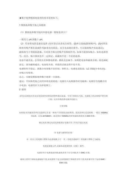
数字地和模拟地处理的基本原则如下:1模拟地和数字地之间链接(1)模拟地和数字地间串接电感一般取值多大?一般用几uH到数十uH。
(2)用0欧电阻是最佳选择 (1)可保证直流电位相等、(2)单点接地(限制噪声)、(3)对所有频率的噪声都有衰减作用(0欧也有阻抗,而且电流路径狭窄,可以限制噪声电流通过)。
磁珠相当于带阻陷波器,只对某个频点的噪声有抑制作用,如果不能预知噪点,如何选择型号,况且,噪点频率也不一定固定,故磁珠不是一个好的选择。
电容不通直流,会导致压差和静电积累,摸机壳会麻手。
如果把电容和磁珠并联,就是画蛇添足,因为磁珠通直,电容将失效。
串联的话就显得不伦不类。
电感特性不稳定,离散分布参数不好控制,体积大。
电感也是陷波,LC 谐振(分布电容),对噪点有特效。
总之,关键是模拟地和数字地要一点接地。
建议,不同种类地之间用0欧电阻相连;电源引入高频器件时用磁珠;高频信号线耦合用小电容;电感用在大功率低频上。
2 磁珠采用在高频段具有良好阻抗特性的铁氧体材料烧结面成,专用于抑制信号线、电源线上的高频噪声和尖峰干扰,还具有吸收静电脉冲的能力。
主要参数:标称值:因为磁珠的单位是按照它在某一频率产生的阻抗来标称的,阻抗的单位也是欧姆 .一般以100MHz为标准,比如2012B601,就是指在100MHz的时候磁珠的阻抗为600欧姆。
额定电流:额定电流是指能保证电路正常工作允许通过电流.3 电感与磁珠的区别:有一匝以上的线圈习惯称为电感线圈,少于一匝(导线直通磁环)的线圈习惯称之为磁珠;电感是储能元件,而磁珠是能量转换(消耗)器件;电感多用于电源滤波回路,磁珠多用于信号回路,用于EMC对策;磁珠主要用于抑制电磁辐射干扰,而电感用于这方面则侧重于抑制传导性干扰.两者都可用于处理EMC、EMI问题;电感一般用于电路的匹配和信号质量的控制上.在模拟地和数字地结合的地方用磁珠.磁珠有很高的电阻率和磁导率,他等效于电阻和电感串联,但电阻值和电感值都随频率变化。
数字地和模拟地处理的基本原则

数字地和模拟地处理的基本原则作者:未知时间:2010-3-17 19:48:03在电子系统设计中,为了少走弯路和节省时间,应充分考虑并满足抗干扰性的要求,避免在设计完成后再去进行抗干扰的补救措施。
形成干扰的基本要素有三个:(1)干扰源,指产生干扰的元件、设备或信号,用数学语言描述如下:du/dt,di/dt大的地方就是干扰源。
如:雷电、继电器、可控硅、电机、高频时钟等都可能成为干扰源。
(2)传播路径,指干扰从干扰源传播到敏感器件的通路或媒介。
典型的干扰传播路径是通过导线的传导和空间的辐射。
(3)敏感器件,指容易被干扰的对象。
如:A/D、D/A变换器,单片机,数字IC,弱信号放大器等。
抗干扰设计的基本原则是:抑制干扰源,切断干扰传播路径,提高敏感器件的抗干扰性能。
(类似于传染病的预防)1 抑制干扰源抑制干扰源就是尽可能的减小干扰源的du/dt,di/dt。
这是抗干扰设计中最优先考虑和最重要的原则,常常会起到事半功倍的效果。
减小干扰源的du/dt主要是通过在干扰源两端并联电容来实现。
减小干扰源的di/dt则是在干扰源回路串联电感或电阻以及增加续流二极管来实现。
抑制干扰源的常用措施如下:(1)继电器线圈增加续流二极管,消除断开线圈时产生的反电动势干扰。
仅加续流二极管会使继电器的断开时间滞后,增加稳压二极管后继电器在单位时间内可动作更多的次数。
(2)在继电器接点两端并接火花抑制电路(一般是RC串联电路,电阻一般选几K 到几十K,电容选0.01uF),减小电火花影响。
(3)给电机加滤波电路,注意电容、电感引线要尽量短。
(4)电路板上每个IC要并接一个0.01μF~0.1μF高频电容,以减小IC对电源的影响。
注意高频电容的布线,连线应靠近电源端并尽量粗短,否则,等于增大了电容的等效串联电阻,会影响滤波效果。
(5)布线时避免90度折线,减少高频噪声发射。
(6)可控硅两端并接RC抑制电路,减小可控硅产生的噪声(这个噪声严重时可能会把可控硅击穿的)。
模拟地与数字地的问题
模拟地与数字地隔离问题模拟电路与数字电路分别辅铜,最后可以用一个10uH电感或0欧姆电阻连起来。
模拟部分的器件尽量集中,放置在与其它板子接口的附近,减小信号衰减。
数字部分线路长一些没关系。
先对模拟地敷铜,然后对整个板敷数字地。
模拟地和数字地之间会自动分隔,用一个1uH的电感或0欧的电阻作为共地点。
2在电子系统设计中,为了少走弯路和节省时间,应充分考虑并满足抗干扰性的要求,避免在设计完成后再去进行抗干扰的补救措施。
:抗干扰设计的基本原则是:抑制干扰源,切断干扰传播路径,提高敏感器件的抗干扰性能。
1 抑制干扰源抑制干扰源的常用措施如下:(1)继电器线圈增加续流二极管,消除断开线圈时产生的反电动势干扰。
仅加续流二极管会使继电器的断开时间滞后,增加稳压二极管后继电器在单位时间内可动作更多的次数。
(2)在继电器接点两端并接火花抑制电路(一般是RC串联电路,电阻一般选几K 到几十K,电容选0.01uF),减小电火花影响。
(3)给电机加滤波电路,注意电容、电感引线要尽量短。
(4)电路板上每个IC要并接一个0.01μF~0.1μF高频电容,以减小IC对电源的影响。
注意高频电容的布线,连线应靠近电源端并尽量粗短,否则,等于增大了电容的等效串联电阻,会影响滤波效果。
(5)布线时避免90度折线,减少高频噪声发射。
(6)可控硅两端并接RC抑制电路,减小可控硅产生的噪声(这个噪声严重时可能会把可控硅击穿的)。
2 切断干扰传播路径的常用措施如下:(1)充分考虑电源对单片机的影响。
电源做得好,整个电路的抗干扰就解决了一大半。
许多单片机对电源噪声很敏感, 要给单片机电源加滤波电路或稳压器,以减小电源噪声对单片机的干扰。
比如,可以利用磁珠和电容组成π形滤波电路,当然条件要求不高时也可用100Ω电阻代替磁珠。
(2)如果单片机的I/O口用来控制电机等噪声器件,在I/O口与噪声源之间应加隔离(增加π形滤波电路)。
控制电机等噪声器件,在I/O口与噪声源之间应加隔离(增加π形滤波电路)。
模拟地和数字地的处理
★数字地和模拟地处理的基本原则如下:1模拟地和数字地之间链接(1)模拟地和数字地间串接电感一般取值多大?一般用几uH到数十uH。
(2)用0欧电阻是最佳选择(1)可保证直流电位相等、(2)单点接地(限制噪声)、(3)对所有频率的噪声都有衰减作用(0欧也有阻抗,而且电流路径狭窄,可以限制噪声电流通过)。
磁珠相当于带阻陷波器,只对某个频点的噪声有抑制作用,如果不能预知噪点,如何选择型号,况且,噪点频率也不一定固定,故磁珠不是一个好的选择。
电容不通直流,会导致压差和静电积累,摸机壳会麻手。
如果把电容和磁珠并联,就是画蛇添足,因为磁珠通直,电容将失效。
串联的话就显得不伦不类。
电感特性不稳定,离散分布参数不好控制,体积大。
电感也是陷波,LC谐振(分布电容),对噪点有特效。
总之,关键是模拟地和数字地要一点接地。
建议,不同种类地之间用0欧电阻相连;电源引入高频器件时用磁珠;高频信号线耦合用小电容;电感用在大功率低频上。
2 磁珠采用在高频段具有良好阻抗特性的铁氧体材料烧结面成,专用于抑制信号线、电源线上的高频噪声和尖峰干扰,还具有吸收静电脉冲的能力。
主要参数:标称值:因为磁珠的单位是按照它在某一频率产生的阻抗来标称的,阻抗的单位也是欧姆 .一般以100MHz 为标准,比如2012B601,就是指在100MHz的时候磁珠的阻抗为600欧姆。
额定电流:额定电流是指能保证电路正常工作允许通过电流.3 电感与磁珠的区别:有一匝以上的线圈习惯称为电感线圈,少于一匝(导线直通磁环)的线圈习惯称之为磁珠;电感是储能元件,而磁珠是能量转换(消耗)器件;电感多用于电源滤波回路,磁珠多用于信号回路,用于EMC对策;磁珠主要用于抑制电磁辐射干扰,而电感用于这方面则侧重于抑制传导性干扰.两者都可用于处理EMC、EMI问题;电感一般用于电路的匹配和信号质量的控制上.在模拟地和数字地结合的地方用磁珠.磁珠有很高的电阻率和磁导率,他等效于电阻和电感串联,但电阻值和电感值都随频率变化。
电源地-信号地-数字地-模拟地的处理方式

一般在我们的AD系统里面,都有非常明确的模拟电源/模拟地;数字电源数字地,这些的处理相对比较重要.通常的系统中==1,我们常用10~20欧姆电阻来做个模拟电源和数字电源的隔离,可以从下图中看出,当然,使用分组的隔离电源是最好的选择,但是成本相对较高2,处理模拟地数字地时,最终使用1点接连的办法,这个连接点要选在PCB上的电荷平衡点,以防止出现电压差,这个需要PCB和模拟设计良好的基础及经验3,使用PSRR高的LDO,尽量避免使用DCDC和纹波超过300UV的电源温压器件,当然,我们可以通过差分输入来减少来自电源的干扰4,良好的屏蔽罩同样可以减少外部空间电磁辐射对AD系统的影响,诸如雷达,手机辐射,紫外线等电源地主要是针对电源回路电流所走的路径而言的,一般来说电源地流过的电流较大,而信号地主要是针对两块芯片或者模块之间的通信信号的回流所流过的路径,一般来说信号地流过的电流很小,其实两者都是GND,之所以分开来说,是想让大家明白在布PCB板时要清楚地了解电源及信号回流各自所流过的路径,然后在布板时考虑如何避免电源及信号共用回流路径,如果共用的话,有可能会导致电源地上大的电流会在信号地上产生一个电压差(可以解释为:导线是有阻抗的,只是很小的阻值,但如果所流过的电流较大时,也会在此导线上产生电位差,这也叫共阻抗干扰),使信号地的真实电位高于0V,如果信号地的电位较大时,有可能会使信号本来是高电平的,但却误判为低电平。
当然电源地本来就很不干净,这样做也避免由于干扰使信号误判。
所以将两者地在布线时稍微注意一下,就可以。
一般来说即使在一起也不会产生大的问题,因为数字电路的门限较高。
除了正确进行接地设计、安装,还要正确进行各种不同信号的接地处理。
控制系统中,大致有以下几种地线:(1)数字地:也叫逻辑地,是各种开关量(数字量)信号的零电位。
(2)模拟地:是各种模拟量信号的零电位。
(3)信号地:通常为传感器的地。
(4)交流地:交流供电电源的地线,这种地通常是产生噪声的地。
数字地与模拟地
关于电路中数字地、模拟地的问题我也看过很多资料,但还是有些不太清楚,请大家帮忙讨论讨论。
1。
数字地模拟地应该在板上分开,单点连接,究竟如何单点连接?是在电源入口处用导线将两个平面短接么?2。
有些器件如da,既有模拟电源,模拟地,也有数字电源数字地,那么是否将da放在跨模拟与数字区域的地方呢,在da下方将数字模拟地单点短接呢?也有建议将da芯片所有电源、地都接到模拟上的,小弟有些糊涂了。
3。
我看到有些设计并不分数字电源或模拟电源,只是划分模拟区域和数字区域,好象数字噪声通常只会影响到几倍线宽之内范围。
这模拟地与数据地是该分开,像伺服芯片他还要将电源地和RF模拟地分开,以免电源杂讯影响RF.地的问题,实质是R L C 和频率的问题根据欧姆定律,只要有电流、电阻存在,就会产生电压降,就是你看到的很宽的PCB也是如此。
当不同部分的电源使用相同的导线时,各自的电流产生的电压降就会相互影响,在地线上的表现就是地电位的变化。
这就是为什么要分开走地线。
同样的道理,电源线上也是如此。
所以要做的不仅仅是地要分开。
分开的电源线和地线需要在电源输出端汇合。
同样的问题也在电源部分出现,所以要小心处理。
你所提出来的问题是数字电路工程师常出现的问题,其实只要了解欧姆定律和基尔荷夫的两个定律就能理解这些问题了。
接地问题是困惑电子工程师的普通而又深奥的问题,也是模拟电路的几个关键问题之一。
接地的好坏直接影响到模拟电路的性能、可靠性和稳定性。
接地问题对数字电路应该好一些,只要注意强电、交流电的地别与数字地掺和,将其隔离即可。
数字电路的地与电源的直流地是无法分开的,因为它本身就是一体的。
我先前做过的一块板子,当时因为数字地和模拟地接法错误,所有的输出全没了,DA也烧掉了。
后来将DA的数字地和模拟地短接,问题就解决了。
小弟我做过几块低频的采样的板子,也不太懂数字地和模拟地应该怎样分开,索性就把它们接在一起了,也没出啥毛病。
我看我们这的高工,一般布线数字地一层,模拟地一层,但最后怎么接的我没注意过还有一种习惯就是对低分辨率的DAC器件在设计上比高分辨率的随便些。
电源地,信号地,数字地,模拟地的处理方式

一般在我们的AD系统里面,都有非常明确的模拟电源/模拟地;数字电源数字地,这些的处理相对比较重要.通常的系统中==1,我们常用10~20欧姆电阻来做个模拟电源和数字电源的隔离,可以从下图中看出,当然,使用分组的隔离电源是最好的选择,但是成本相对较高2,处理模拟地数字地时,最终使用1点接连的办法,这个连接点要选在PCB上的电荷平衡点,以防止出现电压差,这个需要PCB和模拟设计良好的基础及经验3,使用PSRR高的LDO,尽量避免使用DCDC和纹波超过300UV的电源温压器件,当然,我们可以通过差分输入来减少来自电源的干扰4,良好的屏蔽罩同样可以减少外部空间电磁辐射对AD系统的影响,诸如雷达,手机辐射,紫外线等电源地主要是针对电源回路电流所走的路径而言的,一般来说电源地流过的电流较大,而信号地主要是针对两块芯片或者模块之间的通信信号的回流所流过的路径,一般来说信号地流过的电流很小,其实两者都是GND,之所以分开来说,是想让大家明白在布PCB板时要清楚地了解电源及信号回流各自所流过的路径,然后在布板时考虑如何避免电源及信号共用回流路径,如果共用的话,有可能会导致电源地上大的电流会在信号地上产生一个电压差(可以解释为:导线是有阻抗的,只是很小的阻值,但如果所流过的电流较大时,也会在此导线上产生电位差,这也叫共阻抗干扰),使信号地的真实电位高于0V,如果信号地的电位较大时,有可能会使信号本来是高电平的,但却误判为低电平。
当然电源地本来就很不干净,这样做也避免由于干扰使信号误判。
所以将两者地在布线时稍微注意一下,就可以。
一般来说即使在一起也不会产生大的问题,因为数字电路的门限较高。
除了正确进行接地设计、安装,还要正确进行各种不同信号的接地处理。
控制系统中,大致有以下几种地线:(1)数字地:也叫逻辑地,是各种开关量(数字量)信号的零电位。
(2)模拟地:是各种模拟量信号的零电位。
(3)信号地:通常为传感器的地。
(4)交流地:交流供电电源的地线,这种地通常是产生噪声的地。
一些常见的电源地 信号地 数字地和模拟地的处理方式总结
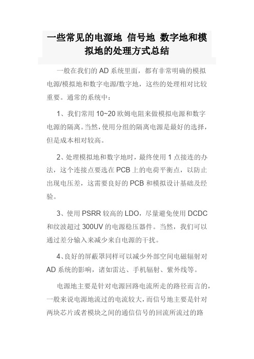
一些常见的电源地信号地数字地和模拟地的处理方式总结一般在我们的AD系统里面,都有非常明确的模拟电源/模拟地和数字电源/数字地,这些的处理相对比较重要。
通常的系统中:1、我们常用10~20欧姆电阻来做模拟电源和数字电源的隔离。
当然,使用分组的隔离电源是最好的选择,但是成本相对较高。
2、处理模拟地和数字地时,最终使用1点接连的办法,这个连接点要选在PCB上的电荷平衡点,以防止出现电压差,这需要良好的PCB和模拟设计基础及经验。
3、使用PSRR较高的LDO,尽量避免使用DCDC 和纹波超过300UV的电源稳压器件。
当然,我们可以通过差分输入来减少来自电源的干扰。
4、良好的屏蔽罩同样可以减少外部空间电磁辐射对AD系统的影响,诸如雷达、手机辐射、紫外线等。
电源地主要是针对电源回路电流所走的路径而言的,一般来说电源地流过的电流较大,而信号地主要是针对两块芯片或者模块之间的通信信号的回流所流过的路径,一般来说信号地流过的电流很小,其实两者都是GND,之所以分开来说,是想让大家明白在布PCB板时要清楚地了解电源及信号回流各自所流过的路径,然后在布板时考虑如何避免电源及信号共用回流路径,如果共用的话,有可能会导致电源地上的大电流在信号地产生一个电压差(可以解释为:导线是有阻抗的,只是阻值很小,但如果所流过的电流较大时,也会在此导线上产生电位差,这也叫共阻抗干扰),使信号地的真实电位高于0V。
信号地的电位较大时,有可能会使本来是高电平的信号被误判为低电平。
当然电源地本来就很不干净,这样做也可以避免由于干扰使信号误判。
所以将电源地和信号地在布线时稍微注意一下,就可以。
一般来说即使在一起也不会产生大的问题,因为数字电路的门限较高。
除了正确进行接地设计、安装,还要正确进行各种不同信号的接地处理。
控制系统中,大致有以下几种地线:(1)数字地:也叫逻辑地,是各种开关量(数字量)信号的零电位。
(2)模拟地:是各种模拟量信号的零电位。
数字地模拟地隔离

数字地和模仿地处理的基起源基础则如下:【1 】1模仿地和数字地之间链接(1)模仿地和数字地间串接电感一般取值多大?一般用几uH到数十uH.(2)用0欧电阻是最佳选择 (1)可包管直流电位相等.(2)单点接地(限制噪声).(3)对所有频率的噪声都有衰减感化(0欧也有阻抗,并且电流路径狭小,可以限制噪声电流畅过).磁珠相当于带阻陷波器,只对某个频点的噪声有克制造用,假如不克不及预知噪点,若何选择型号,何况,噪点频率也不一定固定,故磁珠不是一个好的选择.电容不通直流,会导致压差和静电积聚,摸机壳会麻手.假如把电容和磁珠并联,就是画蛇添足,因为磁珠通直,电容将掉效.串联的话就显得不伦不类.电感特征不稳固,离散散布参数不好掌握,体积大.电感也是陷波,LC谐振(散布电容),对噪点有特效.总之,症结是模仿地和数字地要一点接地.建议,不合种类地之间用0欧电阻相连;电源引入高频器件时用磁珠;高频旌旗灯号线耦合用小电容;电感用在大功率低频上.2 磁珠采取在高频段具有优越阻抗特征的铁氧体材料烧结面成,专用于克制旌旗灯号线.电源线上的高频噪声和尖峰干扰,还具有接收静电脉冲的才能.重要参数:标称值:因为磁珠的单位是按照它在某一频率产生的阻抗来标称的,阻抗的单位也是欧姆 .一般以100MHz为尺度,比方2012B601,就是指在100MHz的时刻磁珠的阻抗为600欧姆.额定电流:额定电流是指能包管电路正常工作许可经由过程电流.3 电感与磁珠的差别:有一匝以上的线圈习惯称为电感线圈,少于一匝(导线纵贯磁环)的线圈习惯称之为磁珠;电感是储能元件,而磁珠是能量转换(消费)器件;电感多用于电源滤波回路,磁珠多用于旌旗灯号回路,用于EMC对策;磁珠重要用于克制电磁辐射干扰,而电感用于这方面则着重于克制传导性干扰.两者都可用于处理EMC.EMI问题;电感一般用于电路的匹配和旌旗灯号质量的掌握上.在模仿地和数字地联合的地方用磁珠.磁珠有很高的电阻率和磁导率,他等效于电阻和电感串联,但电阻值和电感值都随频率变更.他比通俗的电感有更好的高频滤波特征,在高频时呈现阻性,所以能在相当宽的频率规模内保持较高的阻抗,从而进步调频滤波后果.作为电源滤波,可以运用电感.磁珠的电路符号就是电感但是型号上可以看出运用的是磁珠在电路功效上,磁珠和电感是道理雷同的,只是频率特征不合罢了磁珠由氧磁体构成,电感由磁心和线圈构成,磁珠把交换旌旗灯号转化为热能,电感把交换存储起来,迟缓的释放出去.磁珠对高频旌旗灯号才有较大阻碍感化,一般规格有100欧/100mMHZ ,它在低频时电阻比电感小得多.铁氧体磁珠 (Ferrite Bead) 是今朝运用成长很快的一种抗干扰组件,便宜.易用,滤除高频噪声后果明显.在电路中只要导线穿过它即可(我用的都是象通俗电阻模样的,导线已穿过并胶合,也有概况贴装的情势,但很少见到卖的).当导线中电流穿过时,铁氧体对低频电流几乎没有什么阻抗,而对较高频率的电流会产生较大衰减感化.高频电流在个中以热量情势披发,其等效电路为一个电感和一个电阻串联,两个组件的值都与磁珠的长度成比例.磁珠种类许多,制造商应供给技巧指标解释,特殊是磁珠的阻抗与频率关系的曲线.电感和磁珠的什么接洽与差别电感是储能元件,而磁珠是能量转换(消费)器件电感多用于电源滤波回路,磁珠多用于旌旗灯号回路,用于EMC对策磁珠重要用于克制电磁辐射干扰,而电感用于这方面则着重于克制传导性干扰.两者都可用于处理EMC.EMI问题.磁珠是用来接收超高频旌旗灯号,象一些RF电路,PLL,振荡电路,含超高频存储器电路(DDR SDRAM,RAMBUS等)都须要在电源输入部分加磁珠,而电感是一种蓄能元件,用在LC振荡电路,中低频的滤波电路等,其运用频率规模很少超出错50MHZ.★地的衔接一般用电感,电源的衔接也用电感,而对旌旗灯号线则采取磁珠?但现实上磁珠应当也能达到接收高频干扰的目标啊?并且电感在高频谐振今后都不克不及复兴电感的感化了……先必须明确EMI的两个门路,即:辐射和传导,不合的门路采取不合的克制办法.前者用磁珠,后者用电感.对于扳子的IO部分,是不是基于EMC的目标可以用电感将IO部分和扳子的地进行隔离,比方将USB的地和扳子的地用10uH的电感隔离可以防止插拔的噪声干扰地平面?电感一般用于电路的匹配和旌旗灯号质量的掌握上.在模仿地和数字地联合的地方用磁珠.在模仿地和数字地联合的地方用磁珠.数字地和模仿地之间的磁珠用多大磁珠的大小(确实的说应当是磁珠的特征曲线)取决于你须要磁珠接收的干扰波的频率为什么磁珠的单位和电阻是一样的呢??都是欧姆!!磁珠就是阻高频嘛,对直流电阻低,对高频电阻高,不就好懂得了吗,比方1000R@100Mhz就是说对100M频率的旌旗灯号有1000欧姆的电阻因为磁珠的单位是按照它在某一频率产生的阻抗来标称的,阻抗的单位也是欧姆.磁珠的datasheet上一般会附有频率和阻抗的特征曲线图.一般以100MHz为尺度,比方2012B601,就是指在100MHz的时刻磁珠的Impedance为600欧姆.在许多产品中,交换机的两个地用电容衔接起来,为什么不必电感?你说的两个地,个中一个是不是机壳的?我估量(以下全体估量,有错请指导)假如用磁珠或者直接相连的话,人体静电等不测电平会随意马虎进入交换机的地,如许交换机工作就不正常了.但假如它们之间断开,那么遭遇雷击或者其他高压的时刻,两个地之间的电火花引起起火……加电容则防止这种情形.对于加电容的解释我也以为很勉强呵呵,请高手指教!交换机的地,是经由过程两个地之间的之间的电容去清除谐波.就像高阻抗的变压器一样,他附加了一个清除谐波的通路!我本身以为!请斧正!铁氧体材料是铁镁合金或铁镍合金,这种材料具有很高的导磁率,他可所以电感的线圈绕组之间在高频高阻的情形下产生的电容最小.铁氧体材料平日在高频情形下运用,因为在低频时他们重要程电感特征,使得线上的损耗很小.在高频情形下,他们重要呈电抗特征比并且随频率转变.现实运用中,铁氧体材料是作为射频电路的高频衰减器运用的.现实上,铁氧体较好的等效于电阻以及电感的并联,低频下电阻被电感短路,高频下电感阻抗变得相当高,以至于电流全体经由过程电阻.铁氧体是一个消费装配,高频能量在上面转化为热能,这是由他的电阻特征决议的.线圈,磁珠有一匝以上的线圈习惯称为电感线圈,少于一匝(导线纵贯磁环)的线圈习惯称之为磁珠.用处由起所需电感量决议.就教:对于骅讯的USB声卡计划中,在UBS电源端与地端也分离接有一个磁珠,不知是否有人清晰,但是在现实临盆中也有些工程把磁珠用电感去代替了,请问如许可以吗?那边的磁珠是起什么感化哟?作为电源滤波,可以运用电感.磁珠的电路符号就是电感但是型号上可以看出运用的是磁珠在电路功效上,磁珠和电感是道理雷同的,只是频率特征不合罢了★数字地和模仿地处理的基起源基础则如下:1).若为低频模仿电路,加粗和缩短地线;单点接地,可有用防止因为地线公共阻抗而导致的部件之间的互相关扰.而高频电路和数字电路,地线的电感效应较轻微,单点接地会导致现实地线加长,故应多点接地和单点接地相联合.2).高频电路还应斟酌若何克制高频辐射噪声.办法如下:应尽量加粗地线,以降低噪声对地阻抗;大面积(满)接地,即除传输旌旗灯号及电源的印制线以外,其余部分全覆铜作为地线,但不要留有逝世的无用大面积铜箔.3).地线应构成环路,以防止产生高频辐射噪声,但环路面积不成过大,以免产生较大的感应电流.留意若为低频电路,则应防止地线环路.4).数字电源和模仿电源最好隔离,地线离开安插,假如有A/D转换电路,则只在尽量接近该器件处单点接地.1).若为低频模仿电路,加粗和缩短地线;单点接地,可有用防止因为地线公共阻抗而导致的部件之间的互相关扰.而高频电路和数字电路,地线的电感效应较轻微,单点接地会导致现实地线加长,故应多点接地和单点接地相联合.2).高频电路还应斟酌若何克制高频辐射噪声.办法如下:应尽量加粗地线,以降低噪声对地阻抗;大面积(满)接地,即除传输旌旗灯号及电源的印制线以外,其余部分全覆铜作为地线,但不要留有逝世的无用大面积铜箔.3).地线应构成环路,以防止产生高频辐射噪声,但环路面积不成过大,以免产生较大的感应电流.留意若为低频电路,则应防止地线环路.4).数字电源和模仿电源最好隔离,地线离开安插,假如有A/D转换电路,则只在尽量接近该器件处单点接地.问题:数字地和模地低之间应当想一些办法进行隔离噪声,我搜到的办法有接0电阻,电感,电容和磁珠,不知道哪种办法比较好,各是针对什么情形运用的?别的,我的电路有器件正好数字地和模仿地在一路,那该怎么办?感谢列位高手指导!答复:磁珠的等效电路相当于带阻限波器,只对某个频点的噪声有明显克制造用,运用时须要预先估量噪点频率,以便选用恰当型号.对于频率不肯定或无法预知的情形, 磁珠不合.电容隔纵贯交,造成浮地(模仿地和数字地没有接在一路,消失压差,轻易积聚电荷,造成静电).电感体积大,杂散参数多,不稳固. 0欧电阻相当于很窄的电流畅路,可以或许有用地限制环路电流,使噪声得到克制.电阻在所有频带上都有衰减感化(0欧电阻也有阻抗),这点比磁珠强.。
模拟地与数字地隔离问题
模拟地与数字地隔离问题关于数字地与模拟地的隔离问题1.数字电路的频率高,模拟电路的敏感度强,对信号线来说,高频的信号线尽可能远离敏感的模拟电路器件,对地线来说,整个PCB对外界只有一个结点,所以必须在PCB内部进行处理数、模共地的问题,而在板内部数字地和模拟地实际上是分开的它们之间互不相连,只是在PCB与外界连接的接口处(如插头等)。
数字地与模拟地有一点短接,请注意,只有一个连接点。
也有在PCB上不共地的,这由系统设计来决定。
但是,制做PCB板时一般都做铺铜走线,而走线都与GND相联,请问,铺铜之后,模拟地和数字地还能区分出来吗,还能像上面说的那样,只有一个联接点吗?两个地起不同的名字,分别辅铜,最后可以用一个10uH电感或0欧姆电阻连起来。
模拟部分的器件尽量集中,放置在与其它板子接口的附近,减小信号衰减。
数字部分线路长一些没关系。
先对模拟地敷铜,然后对整个板敷数字地。
模拟地和数字地之间会自动分隔,用一个1uH的电感或0欧的电阻作为共地点。
2在电子系统设计中,为了少走弯路和节省时间,应充分考虑并满足抗干扰性的要求,避免在设计完成后再去进行抗干扰的补救措施。
形成干扰的基本要素有三个:(1)干扰源,指产生干扰的元件、设备或信号,用数学语言描述如下:du/dt, di/dt大的地方就是干扰源。
如:雷电、继电器、可控硅、电机、高频时钟等都可能成为干扰源。
(2)传播路径,指干扰从干扰源传播到敏感器件的通路或媒介。
典型的干扰传播路径是通过导线的传导和空间的辐射。
(3)敏感器件,指容易被干扰的对象。
如:A/D、D/A变换器,单片机,数字IC,弱信号放大器等。
抗干扰设计的基本原则是:抑制干扰源,切断干扰传播路径,提高敏感器件的抗干扰性能。
(类似于传染病的预防)1 抑制干扰源抑制干扰源就是尽可能的减小干扰源的du/dt,di/dt。
这是抗干扰设计中最优先考虑和最重要的原则,常常会起到事半功倍的效果。
减小干扰源的du/dt主要是通过在干扰源两端并联电容来实现。
数字地模拟地隔离(2020年7月整理).pdf

数字地和模拟地处理的基本原则如下:1模拟地和数字地之间链接(1)模拟地和数字地间串接电感一般取值多大?一般用几uH到数十uH。
(2)用0欧电阻是最佳选择 (1)可保证直流电位相等、(2)单点接地(限制噪声)、(3)对所有频率的噪声都有衰减作用(0欧也有阻抗,而且电流路径狭窄,可以限制噪声电流通过)。
磁珠相当于带阻陷波器,只对某个频点的噪声有抑制作用,如果不能预知噪点,如何选择型号,况且,噪点频率也不一定固定,故磁珠不是一个好的选择。
电容不通直流,会导致压差和静电积累,摸机壳会麻手。
如果把电容和磁珠并联,就是画蛇添足,因为磁珠通直,电容将失效。
串联的话就显得不伦不类。
电感特性不稳定,离散分布参数不好控制,体积大。
电感也是陷波,LC谐振(分布电容),对噪点有特效。
总之,关键是模拟地和数字地要一点接地。
建议,不同种类地之间用0欧电阻相连;电源引入高频器件时用磁珠;高频信号线耦合用小电容;电感用在大功率低频上。
2 磁珠采用在高频段具有良好阻抗特性的铁氧体材料烧结面成,专用于抑制信号线、电源线上的高频噪声和尖峰干扰,还具有吸收静电脉冲的能力。
主要参数:标称值:因为磁珠的单位是按照它在某一频率产生的阻抗来标称的,阻抗的单位也是欧姆 .一般以100MHz为标准,比如2012B601,就是指在100MHz的时候磁珠的阻抗为600欧姆。
额定电流:额定电流是指能保证电路正常工作允许通过电流.3 电感与磁珠的区别:有一匝以上的线圈习惯称为电感线圈,少于一匝(导线直通磁环)的线圈习惯称之为磁珠;电感是储能元件,而磁珠是能量转换(消耗)器件;电感多用于电源滤波回路,磁珠多用于信号回路,用于EMC对策;磁珠主要用于抑制电磁辐射干扰,而电感用于这方面则侧重于抑制传导性干扰.两者都可用于处理EMC、EMI问题;电感一般用于电路的匹配和信号质量的控制上.在模拟地和数字地结合的地方用磁珠.磁珠有很高的电阻率和磁导率,他等效于电阻和电感串联,但电阻值和电感值都随频率变化。
- 1、下载文档前请自行甄别文档内容的完整性,平台不提供额外的编辑、内容补充、找答案等附加服务。
- 2、"仅部分预览"的文档,不可在线预览部分如存在完整性等问题,可反馈申请退款(可完整预览的文档不适用该条件!)。
- 3、如文档侵犯您的权益,请联系客服反馈,我们会尽快为您处理(人工客服工作时间:9:00-18:30)。
数字地和模拟地应怎样处理
The name "DGND" on an IC tells us that this pin connects to the digital ground of the IC.
一个IC中的“DGND”表示这个脚是连接到该IC内部的数字地。
This does not imply that this pin must be connected to the digital ground of the syste m.
但这并不意味着该脚必须接到系统的数字地。
It is true that this arrangement may inject a small amount of digital noise onto the an alog
ground plane.
这样的安排,的确会将少量的数字噪声引入到模拟地平面中。
These currents should be quite small, and can be minimized by ensuring
that the converter output does not drive a large fanout (they normally can't, by desig n).
然而,IC的数字地电流应该是非常小的。
并且,通过确保(模数)转换器的(数字)输出不驱动重负载
可以使IC的数字地电流达到最小。
Minimizing the fanout on the converter's digital port will also keep the converter logi c
transitions relatively free from ringing and minimize digital switching currents, and thereby reducing any potential coupling into the analog port of the converter.
减少转换器的数字端口负载(注:原文为扇出,就是同时驱动多少个门的意思,我翻译为负载,
负载包括动态和静态的)还可以减少翻转电流和避免出现振铃,这就减少了任何潜在的耦合
混入到转换起的模拟端口中。
The logic supply pin (VD) can be further isolated from the analog supply by the inserti on
of a small lossy ferrite bead as shown in Figure 9.26.
如图9.26所示,通过插入一个有损耗的小铁氧体磁珠,数字电源(VD)可以进一步与模拟电源隔离。
The internal transient digital currents of the converter will flow in the small loop from VD through the decoupling capacitor and to DGND (this path is shown with a heavy li ne on
the diagram).
转换器内部的数字毛刺电流将从VD通过退耦电容到DGND这个小环路流过(该路径在图中用粗线标出)。
The transient digital currents will therefore not appear on the external analog ground plane,
but are confined to the loop.
因此,数字毛刺电流不会在外面的模拟地平面中出现,仅被限制在该小环内。
The VD pin decoupling capacitor should be mounted as close to the converter as possible to minimize parasitic inductance.
VD引脚的退耦电容应该尽可能的靠近转换器放置,以使寄生电感最小。
These decoupling capacitors should be low inductance ceramic types,
typically between 0.01 μF and 0.1 μF.
这些退耦电容应该是低感抗的陶瓷电容,容量通常在0.01uF到0.1uF之间。
Inside an IC that has both analog and digital circuits, such as an ADC or a DAC, the grounds are usually kept separate to avoid coupling digital signals into the analog circuits.
在既有模拟电路又有数字电路的IC内部(例如ADC或者DAC),数字地和模拟地通常是分开的以避免
数字信号耦合到模拟电路中。
Figure 9.26 shows a simple model of a converter.
图9.26给出了一个转换器的简易模型。
There is nothing the IC designer can do about the wirebond inductance and resistanc e
associated with connecting the bond pads on the chip to the package pins except to realize it's there.
IC设计人员对于连接芯片和封装引脚之间的绑定线的电感和电阻,除了知道它的存在之外,无计可施。
The rapidly changing digital currents produce a voltage at point B which will inevitabl y
couple into point A of the analog circuits through the stray capacitance, CSTRAY.
迅速变化的数字电流在B点产生一个电压,它将不可避免的通过寄生电容C STRAY 耦合到模拟电路的A点。
In addition, there is approximately 0.2-pF unavoidable stray capacitance between eve ry
pin of the IC package! It's the IC designer's job to make the chip work in spite of this. 另外,在IC封装的引脚之间,不可避免的存在着约0.2pF的寄生电容。
IC设计者有义务让芯片在这种条件下
也能很好的工作。
However, in order to prevent further coupling, the AGND and DGND pins should be j oined
together externally to the analog ground plane with minimum lead lengths.
然而,为了避免更多的耦合,AGND和DGND引脚应该在外部连在一起并通过最短的引线连接到模拟地平面。
Any extra impedance in the DGND connection will cause more digital noise to be dev eloped
at point B; it will, in turn, couple more digital noise into the analog circuit through the stray capacitance.
任何额外的DGND连接阻抗将会导致B点出现更多的数字噪声;通过寄生电容,这将会有更多的数字噪声
耦合到模拟电路中。
Note that connecting DGND to the digital ground plane applies VNOISE across the AGND and DGND pins and invites disaster!
注意,连接DGND到数字地平面将会把VNOISE引入到AGND和DGND并惹来天灾!。