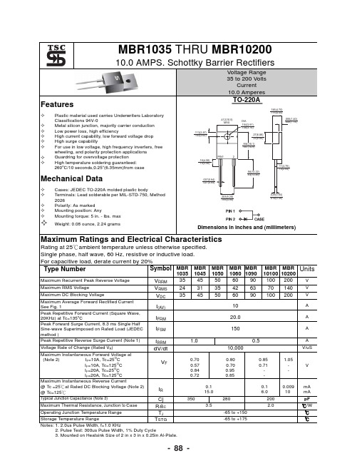
MBR1035中文资料
CPC1035N;中文规格书,Datasheet资料

IF = 5mA
0.8 -40 -20
0 20 40 60 80 100 120 Temperature (ºC)
Turn-On (ms)
Typical Turn-On vs. Temperature
(I =50mA) L
5.0
4.5
4.0
3.5
3.0
2.5
2.0
1.5
IF = 5mA
1.0
0.5
0 -40 -20 0
1 Derate linearly 3.33 mW / ºC
Ratings 350 5 50 1 70 400 1500
-40 to +85 -40 to +125
Units VP V mA A mW mW Vrms °C °C
CPC1035N
Absolute Maximum Ratings are stress ratings. Stresses in excess of these ratings can cause permanent damage to the device. Functional operation of the device at conditions beyond those indicated in the operational sections of this data sheet is not implied.
5 10 15 20 25 30 35 40 45 50 LED Forward Current (mA)
Typical LED Forward Voltage Drop vs. Temperature
1.8
1.6
1.4
IF = 50mA
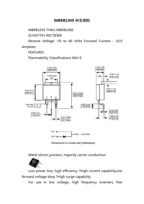
MBR1045CT中文资料
@ TC = 105°C
Non-Repetitive Peak Forward Surge Current 8.3ms Single half sine-wave superimposed on rated load (JEDEC Method)
Repetitive Peak Reverse Surge Current
B
C D
K
L M
A
12 3
E
G
J
N
HH
Pin 1 Pin 2 Pin 3
P
Case
TO-220AB
Dim Min Max
A 14.22 15.88
B
9.65 10.67
C
2.54 3.43
D
5.84 6.86
E
¾
6.35
G 12.70 14.73
H
2.29 2.79
J
0.51 1.14
K 3.53Æ 4.09Æ
DS30027 Rev. A-2
1 of 2
MBR1030CT-MBR1060CT
元器件交易网
10
I(AV), AVERAGE FWD CURRENT (A)
8 6
4
IFSM, PEAK FORWARD SURGE CURRENT (A)
2
0 0
50
100
150
TC, CASE TEMPERATURE (°C) Fig. 1 Forward Current Derating Curve
Mechanical Data
· Case: Molded Plastic · Terminals: Plated Leads Solderable per
ON SEMICONDUCTOR MBRD1035CTL 数据手册
MBRD1035CTL SWITCHMODE tSchottky Power Rectifier DPAK Power Surface Mount PackageThe MBRD1035CTL employs the Schottky Barrier principle in a large area metal−to−silicon power diode. State of the art geometryfeatures epitaxial construction with oxide passivation and metal overlay contact. Ideally suited for low voltage, high frequency switching power supplies, free wheeling diode and polarity protection diodes.Features•Highly Stable Oxide Passivated Junction•Guardring for Stress Protection•Matched Dual Die Construction −May be Paralleled for High Current Output•High dv/dt Capability•Short Heat Sink Tap Manufactured − Not Sheared•Very Low Forward V oltage Drop•EpoxyMeetsUL94V−*********•Pb−Free Packages are AvailableMechanical Characteristics:•Case: Epoxy, Molded•Weight: 0.4 Gram (Approximately)•Finish: All External Surfaces Corrosion Resistant and Terminal Leads are Readily Solderable•Lead and Mounting Surface Temperature for Soldering Purposes: 260°C Max. for 10 SecondsSCHOTTKY BARRIERRECTIFIER10 AMPERES35 VOLTS134DPAKCASE 369CMARKING DIAGRAM1234YWWB1035CLGY= YearWW= Work WeekB1035CL= Device CodeG= Pb−Free PackageSee detailed ordering and shipping information in the package dimensions section on page 2 of this data sheet.ORDERING INFORMATIONMAXIMUM RATINGSRating Symbol Value UnitPeak Repetitive Reverse Voltage Working Peak Reverse Voltage DC Blocking Voltage V RRMV RWMV R35VAverage Rectified Forward Current Per Leg (At Rated V R, T C = 115°C)Per Package I O 5.010APeak Repetitive Forward Current Per Leg(At Rated V R, Square Wave, 20 kHz, T C = 115°C)I FRM10ANon−Repetitive Peak Surge Current Per Package(Surge applied at rated load conditions, halfwave, single phase, 60 Hz)I FSM50A Storage / Operating Case Temperature T stg,T c−55 to +150°C Operating Junction Temperature (Note 1)T J−55 to +150°C Voltage Rate of Change (Rated V R, T J = 25°C)dv/dt10,000V/m s Maximum ratings are those values beyond which device damage can occur. Maximum ratings applied to the device are individual stress limit values (not normal operating conditions) and are not valid simultaneously. If these limits are exceeded, device functional operation is not implied, damage may occur and reliability may be affected.1.The heat generated must be less than the thermal conductivity from Junction−to−Ambient: dP D/dT J < 1/R q JA.THERMAL CHARACTERISTICSThermal Resistance, Junction−to−Case Per Leg R q JC 3.0°C/W Thermal Resistance, Junction−to−Ambient (Note 2)Per Leg R q JA137°C/W ELECTRICAL CHARACTERISTICSMaximum Instantaneous Forward Voltage (Note 3)(See Figure 2)Per Leg I F = 5 Amps, T J = 25°CI F = 5 Amps, T J = 100°CI F = 10 Amps, T J = 25°CI F = 10 Amps, T J = 100°C V F0.470.410.560.55VMaximum Instantaneous Reverse Current (Note 3)(See Figure 4)Per Leg (V R = 35 V, T J = 25°C)(V R = 35 V, T J = 100°C)(V R = 17.5 V, T J = 25°C)(V R = 17.5 V, T J = 100°C)I R2.0300.205.0mA2.Rating applies when using minimum pad size, FR4 PC Board3.Pulse Test: Pulse Width ≤ 250 m s, Duty Cycle ≤2.0%ORDERING INFORMATIONDevice Package Shipping†MBRD1035CTL DPAK75 Units / RailMBRD1035CTLG DPAK(Pb−Free)75 Units / RailMBRD1035CTLT4DPAK2500 Units / Tape & Reel MBRD1035CTLT4G DPAK(Pb−Free)2500 Units / Tape & Reel†For information on tape and reel specifications, including part orientation and tape sizes, please refer to our Tape and Reel Packaging Specifications Brochure, BRD8011/D.TYPICAL CHARACTERISTICSFigure 2. Maximum Forward Voltage Per LegFigure 3. Typical Reverse Current Per Leg 10010V R , REVERSE VOLTAGE (VOLTS)350I F , I N S T A N T A N E O US F O R W A R D C U R R E N T (A M P S )I 1.01020300.1, R E V E R S E C U R R E N T (A M P S )R Figure 4. Maximum Reverse Current Per LegV F , MAXIMUM INSTANTANEOUS FORWARD VOLTAGE (VOLTS)100I F , I N S T A N T A N E O U S F O R W A R D C U R R E N T (A M P S )V R , REVERSE VOLTAGE (VOLTS)35100E−61E−61020301E−31E+0I , M A X I M U M R E V E R S E C U R R E N T (A M P S )RFigure 7. Capacitance Per Leg8.07.05.06.04.0V R , DC REVERSE VOLTAGE (VOLTS)2500V R , REVERSE VOLTAGE (VOLTS)10010I O , A V E R A G E F O R W A R D C U R R E N T (A M P S )C , C A P A C I T A N C E (p F )3.02.01.03035510152051015202501000)Figure 8. Typical Operating TemperatureDerating Per Leg ** Reverse power dissipation and the possibility of thermal runaway must be considered when operating this device under any re-verse voltage conditions. Calculations of T J therefore must include forward and reverse power effects. The allowable operating T J may be calculated from the equation:T J = T Jmax − r(t)(Pf + Pr) wherer(t) = thermal impedance under given conditions,Pf = forward power dissipation, and Pr = reverse power dissipationThis graph displays the derated allowable T J due to reverse bias under DC conditions only and is calculated as T J = T Jmax − r(t)Pr,where r(t) = Rthja. For other power applications further calculations must be performed.Figure 9. Thermal Response Junction to Case (Per Leg)Figure 10. Thermal Response Junction to Ambient (Per Leg)0.10.00001t, TIME (s)1.00.10.01r 0.00010.0010.01, T R A N S I E N T T H E R M A L R E S I S T A N C E (N O R M A L I Z E D )(t ) 1.01010010000.10.00001t, TIME (s)1.0E+001.0E−011.0E−021.0E−031.0E−040.00010.0010.011.01010010000r , T R A N S I E N T T H E R M A L R E S I S T A N C E (N O R M A L I Z E D )(t )1000PACKAGE DIMENSIONSDPAK (SINGLE GUAGE)CASE 369C ISSUE OVSDIMMIN MAX MIN MAX MILLIMETERSINCHES A 0.2350.245 5.97 6.22B 0.2500.265 6.35 6.73C 0.0860.094 2.19 2.38D 0.0270.0350.690.88E 0.0180.0230.460.58F 0.0370.0450.94 1.14G 0.180 BSC 4.58 BSC H 0.0340.0400.87 1.01J 0.0180.0230.460.58K 0.1020.114 2.60 2.89L 0.090 BSC 2.29 BSC R 0.1800.215 4.57 5.45S 0.0250.0400.63 1.01U 0.020−−−0.51−−−V 0.0350.0500.89 1.27Z0.155−−−3.93−−−NOTES:1.DIMENSIONING AND TOLERANCING PER ANSI Y14.5M, 1982.2.CONTROLLING DIMENSION: INCH.ǒmm inchesǓSCALE 3:1*For additional information on our Pb−Free strategy and solderingdetails, please download the ON Semiconductor Soldering and Mounting Techniques Reference Manual, SOLDERRM/D.SOLDERING FOOTPRINT*ON Semiconductor and are registered trademarks of Semiconductor Components Industries, LLC (SCILLC). SCILLC reserves the right to make changes without further notice to any products herein. SCILLC makes no warranty, representation or guarantee regarding the suitability of its products for any particular purpose, nor does SCILLC assume any liability arising out of the application or use of any product or circuit, and specifically disclaims any and all liability, including without limitation special, consequential or incidental damages.“Typical” parameters which may be provided in SCILLC data sheets and/or specifications can and do vary in different applications and actual performance may vary over time. All operating parameters, including “Typicals” must be validated for each customer application by customer’s technical experts. SCILLC does not convey any license under its patent rights nor the rights of others. SCILLC products are not designed, intended, or authorized for use as components in systems intended for surgical implant into the body, or other applications intended to support or sustain life, or for any other application in which the failure of the SCILLC product could create a situation where personal injury or death may occur. Should Buyer purchase or use SCILLC products for any such unintended or unauthorized application, Buyer shall indemnify and hold SCILLC and its officers, employees, subsidiaries, affiliates,and distributors harmless against all claims, costs, damages, and expenses, and reasonable attorney fees arising out of, directly or indirectly, any claim of personal injury or death associated with such unintended or unauthorized use, even if such claim alleges that SCILLC was negligent regarding the design or manufacture of the part. SCILLC is an Equal Opportunity/Affirmative Action Employer. This literature is subject to all applicable copyright laws and is not for resale in any manner.PUBLICATION ORDERING INFORMATIONSWITCHMODE is a trademark of Semiconductor Components Industries, LLC (SCILLC).。
MBR1050;MBR1045;MBR1060;MBR1035;中文规格书,Datasheet资料
20 10 MBR1035-MBR1045
1
MBR1050-MBR1060
0.1
T A= 125ºC TA = 75º C
0.01
MBR1035-MBR1045
TA = 25º C
0.001 0
MBR1050-MBR1060
20
40
60
80 100 120
Percent of Rated Peak Reverse Voltage [%]
INDUCTIVE LOAD
2 .375" (9.00mm) LOAD
LENGTHS
0 0 25 50 75 100 125 150 175 Ambient Temperature [ºC]
Figure 1. Forward Current Derating Curve
Peak Forward Surge Current, IFSM [A]
0.5
Units
V V V V mA mA A
© 2012 Fairchild Semiconductor Corporation
MBR1035 - MBR1060 Rev. D0
1
/
MBR1035 - MBR1060 — Schottky Rectifie源自s354550
60
V
10
A
150
A
Tstg Storage Temperature Range
-65 to +175
°C
TJ Operating Junction Temperature
-65 to +150
°C
* These ratings are limiting values above which the serviceability of any semiconductor device may be impaired.
MBR1045中文资料

MBR1035-MBR1060MBR1035 - MBR1060, Rev. A©1999 Fairchild Semiconductor CorporationMBR1035 - MBR1060, Rev. ATRADEMARKSACEx™CoolFET™CROSSVOLT™E 2CMOS TM FACT™FACT Quiet Series™FAST ®FASTr™GTO™HiSeC™The following are registered and unregistered trademarks Fairchild Semiconductor owns or is authorized to use and is not intended to be an exhaustive list of all such trademarks.LIFE SUPPORT POLICYFAIRCHILD’S PRODUCTS ARE NOT AUTHORIZED FOR USE AS CRITICAL COMPONENTS IN LIFE SUPPORTDEVICES OR SYSTEMS WITHOUT THE EXPRESS WRITTEN APPROV AL OF FAIRCHILD SEMICONDUCTOR CORPORA TION.As used herein:ISOPLANAR™MICROWIRE™POP™PowerTrench™QS™Quiet Series™SuperSOT™-3SuperSOT™-6SuperSOT™-8TinyLogic™1. Life support devices or systems are devices or systems which, (a) are intended for surgical implant intothe body, or (b) support or sustain life, or (c) whosefailure to perform when properly used in accordancewith instructions for use provided in the labeling, can be reasonably expected to result in significant injury to the user.2. A critical component is any component of a lifesupport device or system whose failure to perform can be reasonably expected to cause the failure of the life support device or system, or to affect its safety or effectiveness.PRODUCT STATUS DEFINITIONS Definition of TermsDatasheet Identification Product Status Definition Advance InformationPreliminary No Identification Needed Obsolete This datasheet contains the design specifications for product development. Specifications may change in any manner without notice.This datasheet contains preliminary data, andsupplementary data will be published at a later date.Fairchild Semiconductor reserves the right to make changes at any time without notice in order to improve design.This datasheet contains final specifications. Fairchild Semiconductor reserves the right to make changes at any time without notice in order to improve design.This datasheet contains specifications on a product that has been discontinued by Fairchild semiconductor.The datasheet is printed for reference information only.Formative or In DesignFirst ProductionFull ProductionNot In ProductionDISCLAIMERFAIRCHILD SEMICONDUCTOR RESERVES THE RIGHT TO MAKE CHANGES WITHOUT FURTHER NOTICE TO ANY PRODUCTS HEREIN TO IMPROVE RELIABILITY , FUNCTION OR DESIGN. FAIRCHILD DOES NOT ASSUME ANY LIABILITY ARISING OUT OF THE APPLICATION OR USE OF ANY PRODUCT OR CIRCUIT DESCRIBED HEREIN; NEITHER DOES IT CONVEY ANY LICENSE UNDER ITS PATENT RIGHTS, NOR THE RIGHTS OF OTHERS.。
MBR性能介绍(中文版)
Toray 公司的膜技术更新2002年12月Toray 公司Toray 公司概况建立于: 销售额: 1926年 1月 1,015,713,000,000 (2001年) 1. 纤维和纺织品:-尼龙, 聚酯,丙烯酸树脂主要业务: 以下产品的生产和销售:2. 塑料制品和化工产品:- 尼龙, ABS, PBT, PPS, POM, LCP 和其它树脂 -聚酯,聚丙烯, PPS,芳族聚酸胺和其它膜材料3. 最新产品业务:- 医药、医疗产品, - 液晶显示器彩色滤膜, - 碳素纤维4. 房地产与工程:- 房屋与建筑材料 - 环保设备 - 膜与水处理系统 - 房地产 - 设备安装与运行工程员工:34,910人 ( 2002年3月31日止 )浸没式膜生物反应器处理流程传统水处理 废水 流程活性污泥 沉淀池 出水浸没式膜分 离处理流程废水膜组件 出水 RO 回用膜生物反应器 (MBR)两种不同方式的比较 工艺流程 传统方法 浸没式 处理效果 弱 极好 维持 弱 好 污泥浓度 低 高 能量消耗 大 小 节约空间 少 极大MBR 组件平板膜元件出水 1,590mm 管口流出支架 进水 515mm 膜 隔层通风MBR 组件M-1 M-2 100 740x1550x2200 600 137 60■组件特性元件数目尺寸大小 [长x宽x高, mm]50 740 x 840 x2200 320 68 30重量 [kg] 面积 [m2] 标准流量 [m3/d]浸没式膜的设计1. 膜材料 聚偏氟乙烯 : PVDF化学稳定性强: 物理强度大:HH n FF含氟 大分子量 (MW=300,000 400,000)2. 膜形态 纤维加固平板膜 3. 表面孔径 1) 孔径小 2) 孔分布密 3) 孔量多PVDF 纤维 膜易渗透,防堵塞 大流量低污染RO膜元件 (TM20L-370/400)主要用途: (1) 城市排水、废水回用 (2) 海水脱盐废 水 处 理 流 程 图废水 沉淀池 流出活性污泥砂滤回用UF/MF低污染 RO特征: (1) 脱盐率: 高于99.5% (2) 产水能力: 32.5 m3/d (NaCl 1,500mg/L,1.5MPa) (3) 抗化学和生物污染10.0 9.0 8.0 7.0 6.0 5.0 4.0 3.0 2.0 1.0 0.0 0 5正常水处理能力 (m3/d/MPa 25℃)低污染 RO传统 RO10 日期 15 20低污染RO和传统 RO对城市二次 排水处理能力的比较联系日本:東レ株式会社 水処理システム事業部 日本千葉県浦安市1丁目8番1号 電話:047-350-6367郵編:279-8555 伝真:047-350-6225上海:东丽 (中国)投资有限公司开发部 上海市浦东新区银城东路101号 汇丰大厦10楼(原上海森茂国际大厦) 电话: 021-6841-1470 传真:021-6841-3220邮编:200120。
MBR产品介绍2010版

膜生物反应器(SMBR)系列产品介绍一、膜-生物反应器(SMBR)技术介绍膜-生物反应器(Membrane Bioreactor,MBR)技术,是一种新型高效的污水处理工艺,它用膜组件代替传统活性污泥法中的二沉池,大大提高了系统固液分离的能力。
MBR技术是膜分离技术与生物技术有机结合的新型废水处理技术。
它利用膜分离组件将生化反应池中的活性污泥和大分子有机物截留住,省掉二沉池。
因此,活性污泥浓度可以大大提高,水力停留时间(HRT)和污泥停留时间(SRT)可以分别控制,而难降解的物质在反应器中不断反应和降解。
因此,膜-生物反应器工艺通过膜的分离技术大大强化了生物反应器的功能。
膜-生物反应器在优化生化作用的优越性:1 对污染物的去除率高,抵抗污泥膨胀能力强,出水水质稳定可靠,出水中没有悬浮物;2 膜生物反应器实现了反应器污泥龄SRT和水力停留时间HRT的彻底分离,设计、操作大大简化;3 膜的机械截流作用避免了微生物的流失,生物反应器内可保持高的污泥浓度,从而能提高体积负荷,降低污泥负荷,且MBR工艺略去了二沉池,大大减少占地面积;4 由于SRT很长,生物反应器又起到了“污泥硝化池”的作用,从而显著减少污泥产量,剩余污泥产量低,污泥处理费用低;5 由于膜的截流作用使SRT延长,营造了有利于增殖缓慢的微生物。
如硝化细菌生长的环境,可以提高系统的硝化能力,同时有利于提高难降解大分子有机物的处理效率和促使其彻底的分解;6 S MBR曝气池的活性污泥不因产水而损失,在运行过程中,活性污泥会因进入有机物浓度的变化而变化,并达到一种动态平衡,这使系统出水稳定并有耐冲击负荷的特点;7 较大的水力循环导致了污水的均匀混合,因而使活性污泥有很好的分散性,大大提高活性污泥的比表面积。
MBR系统中活性污泥的高度分散是提高水处理的效果的又一个原因。
这是普通生化法水处理技术形成较大的菌胶团所难以相比的;8膜生物反应器易于一体化,易于实现自动控制,操作管理方便;SMRB的工艺过程如下:二、聚丙烯(PP)中空纤维膜聚丙烯中空纤维膜(PP)是国际上最新一代膜分离材料。
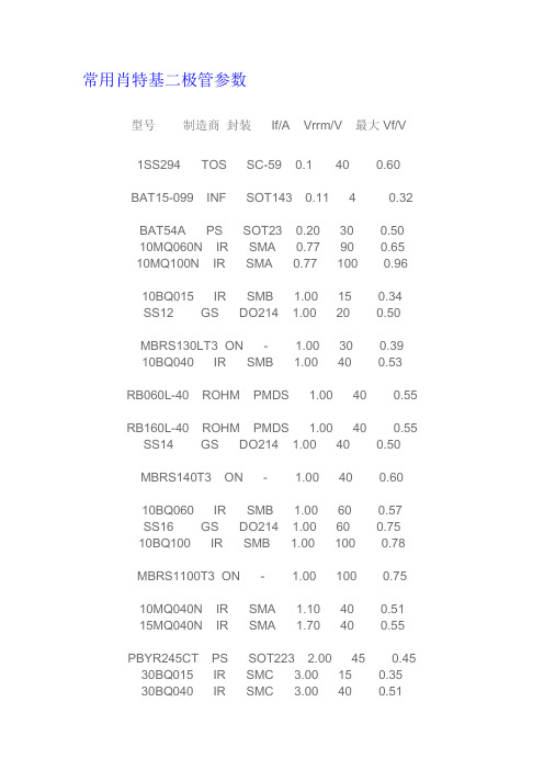
长电二极管参数资料
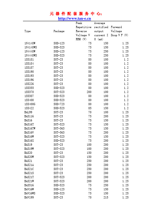
Type Package RepetitiveReverseVoltage VRRM (V)rectifiedoutputcurrent IO (mA)ForwardVoltageDrop V F (V)1N4148W SOD-123 75 150 1.25 1N4148WS SOD-323 75 150 1.25 1N4448W SOD-123 75 250 1.25 1N4448WS SOD-323 75 250 1.25 1SS181 SOT-23 80 100 1.2 1SS184 SOT-23 80 100 1.2 1SS187 SOT-23 80 100 1.2 1SS190 SOT-23 80 100 1.2 1SS193 SOT-23 80 100 1.2 1SS196 SOT-23 80 100 1.2 1SS226 SOT-23 80 100 1.2 1SS355 SOD-323 80 100 1.2 1SS370 SOT-323 200 100 1.2 1SS387 SOD-523 80 100 1.2 1SS400 SOD-523 80 100 1.2 1SS400G SOD-723 80 100 1.2 1SS422 SOD-523 85 150 1.2 BAL99 SOT-23 70 100 1.25 BAS116 SOT-23 75 200 1.25 BAS16 SOT-23 75 150 1.25 BAS16T SOT-523 75 150 1.25 BAS16TW SOT-363 75 150 1.25 BAS16V SOT-563 75 200 1.25 BAS16W SOT-323 75 150 1.25 BAS16X SOD-523 75 200 1.25 BAS19 SOT-23 100 200 1.25 BAS19W SOT-323 100 200 1.25 BAS20 SOT-23 150 200 1.25 BAS20W SOT-323 150 200 1.25 BAS21 SOT-23 250 200 1.25 BAS21A SOT-23 250 200 1.25 BAS21C SOT-23 250 200 1.25 BAS21S SOT-23 250 200 1.25 BAS21T SOT-523 200 200 1.25 BAS21W SOT-323 200 200 1.25 BAS516 SOD-523 75 250 1.25 BAV16W SOD-123 75 150 1.25 BAV16WS SOD-323 75 150 1.25 BAV199 SOT-23 70 215 1.25BAV19W SOD-123 100 200 1.25 BAV19WS SOD-323 100 200 1.25 BAV20W SOD-123 150 200 1.25 BAV20WS SOD-323 150 200 1.25 BAV21W SOD-123 200 200 1.25 BAV21WS SOD-323 200 200 1.25 BAV70 SOT-23 70 200 1.25 BAV70DW SOT-363 75 150 1.25 BAV70T SOT-523 85 75 1.25 BAV70W SOT-323 75 150 1.25 BAV74 SOT-23 50 200 1 BAV756DW SOT-363 75 150 1.25 BAV99 SOT-23 70 200 1.25 BAV99BRW SOT-363 75 150 1.25 BAV99DW SOT-363 75 150 1.25 BAV99T SOT-523 85 75 1.25 BAV99W SOT-323 75 150 1.25 BAW56 SOT-23 70 200 1.25 BAW567DW SOT-363 75 150 1.25 BAW56DW SOT-363 75 150 1.25 BAW56T SOT-523 85 75 1.25 BAW56W SOT-323 75 150 1.25 CMSD2004S SOT-23 240 200 1 DA204U SOT-323 20 100 1 DA221 SOT-523 20 100 1 DAN202U SOT-323 80 100 1.2 DAN217 SOT-23 80 100 1.2 DAN217U SOT-323 80 100 1.2 DAN222 SOT-523 80 100 1.2 DAP202U SOT-323 80 100 1.2 DAP222 SOT-523 80 100 1.2 DK16LLD03 WBFBP-03D 75 150 1.25 DK21LLD03 WBFBP-03D 200 200 1.25 DK400LED02 WBFBP-02C 80 100 1.2 DK4148LLD03 WBFBP-03D 75 150 1.25 DK4148NND03 WBFBP-03B 75 150 1.25 DK4148TTD03 WBFBP-03A 75 150 1.25 DK4448CLLD03 WBFBP-03D 80 250 1.25 DK4448LLD03 WBFBP-03D 80 250 1.25 DK70LLD03 WBFBP-03D 85 75 1.25 DK914LLD03 WBFBP-03D 100 300 1.25 DKN222LLD03 WBFBP-03D 80 100 1.2 DKN222NN03 WBFBP-03B 80 100 1.2MC2836 SOT-23 50 150 1.2 MC2838 SOT-23 50 100 1.2 MMBD4148 SOT-23 75 150 1.25 MMBD4148A SOT-23 100 200 1 MMBD4148CA SOT-23 100 200 1 MMBD4148CC SOT-23 100 200 1 MMBD4148SE SOT-23 100 200 1 MMBD4148T SOT-523 75 150 1.25 MMBD4148TW SOT-363 75 150 1.25 MMBD4148W SOT-323 75 150 1.25 MMBD4448DW SOT-363 75 250 1.25 MMBD4448HADW SOT-363 80 250 1.25 MMBD4448HAQW SOT-363 80 250 1.25 MMBD4448HCDW SOT-363 80 250 1.25 MMBD4448HSDW SOT-363 80 250 1.25 MMBD4448HT SOT-523 80 250 1.25 MMBD4448HTA SOT-523 80 250 1.25 MMBD4448HTC SOT-523 80 250 1.25 MMBD4448HTS SOT-523 80 250 1.25 MMBD4448HTW SOT-363 80 250 1.25 MMBD4448V SOT-563 80 250 1.25 MMBD4448W SOT-323 75 250 1.25 MMBD7000 SOT-23 100 200 1.1 MMBD914 SOT-23 100 300 1.251N5817 SOT-23-3L 20 1000 0.75 1N5819 SOT-23-3L 40 1000 0.9 1SS357 SOD-323 40 100 0.6 1SS388 SOD-523 40 100 0.6 1SS401 SOT-323 20 300 0.45 1SS404 SOD-323 20 300 0.45 B0520LW SOD-123 20 500 0.385 B0530W SOD-123 30 500 0.43 B0540W SOD-123 40 500 0.62 B5817W SOD-123 20 1000 0.75 B5817WS SOD-323 20 1000 0.75 B5818W SOD-123 30 1000 0.875 B5818WS SOD-323 30 1000 0.875 B5819W SOD-123 40 1000 0.9 B5819WS SOD-323 40 1000 0.9 BAS40 SOT-23 40 200 1 BAS40-04 SOT-23 40 200 1 BAS40-04T SOT-523 40 200 1BAS40-05T SOT-523 40 200 1 BAS40-06 SOT-23 40 200 1 BAS40-06T SOT-523 40 200 1 BAS40T SOT-523 40 200 1 BAS40V SOT-563 40 200 1 BAS40W SOT-323 40 200 1 BAS40W-04 SOT-323 40 200 1 BAS40W-05 SOT-323 40 200 1 BAS40W-06 SOT-323 40 200 1 BAS40WS SOD-323 40 200 1 BAS70 SOT-23 70 70 1 BAS70-04 SOT-23 70 70 1 BAS70-04T SOT-523 70 70 1 BAS70-05 SOT-23 70 70 1 BAS70-05T SOT-523 70 70 1 BAS70-06 SOT-23 70 70 1 BAS70-06T SOT-523 70 70 1 BAS70T SOT-523 70 70 1 BAS70W SOT-323 70 70 1 BAS70W-04 SOT-323 70 70 1 BAS70W-05 SOT-323 70 70 1 BAS70W-06 SOT-323 70 70 1 BAS70WS SOD-323 70 70 1 BAT42W SOD-123 30 200 0.65 BAT42WS SOD-323 30 200 0.65 BAT43W SOD-123 30 200 0.45 BAT43WS SOD-323 30 200 0.45 BAT54 SOT-23 30 200 1 BAT54A SOT-23 30 200 1 BAT54AT SOT-523 30 200 1 BAT54AW SOT-323 30 200 1 BAT54C SOT-23 30 200 1 BAT54CT SOT-523 30 200 1 BAT54CW SOT-323 30 200 1 BAT54S SOT-23 30 200 1 BAT54ST SOT-523 30 200 1 BAT54SW SOT-323 30 200 1 BAT54T SOT-523 30 200 1 BAT54V SOT-563 30 200 1 BAT54W SOT-323 30 200 1 BAT54WS SOD-323 30 100 1 BAT54X SOD-523 30 200 0.8 BTA60B SOD-323 10 3000 0.6DS521-30LED02 WBFBP-02C 30 100 0.35 DS54NND03 WBFBP-03B 30 200 1 DS715NND03 WBFBP-03B 30 30 0.37 DS751-40LED02 WBFBP-02C 40 30 0.37 MBR10100 TO-220AC 100 10000 0.8 MBR10100CT TO-220-3L 100 10000 0.85 MBR1030CT TO-220-3L 30 10000 0.7 MBR1035CT TO-220-3L 35 10000 0.7 MBR1040CT TO-220-3L 40 10000 0.7 MBR1045CT TO-220-3L 45 10000 0.7 MBR1050CT TO-220-3L 50 10000 0.8 MBR1060CT TO-220-3L 60 10000 0.8 MBR1530CT TO-220-3L 30 15000 0.7 MBR1535CT TO-220-3L 35 15000 0.7 MBR1540CT TO-220-3L 40 15000 0.7 MBR1545CT TO-220-3L 45 15000 0.7 MBR1550CT TO-220-3L 50 15000 0.75 MBR1560CT TO-220-3L 60 15000 0.75 MBR20100CT TO-220-3L 100 20000 0.85 MBR20150CT TO-220-3L 150 20000 0.9 MBR20200CT TO-220-3L 200 20000 0.9 MBR2030CT TO-220-3L 30 20000 0.7 MBR2035CT TO-220-3L 35 20000 0.7 MBR2040CT TO-220-3L 40 20000 0.7 MBR2045CT TO-220-3L 45 20000 0.7 MBR2050CT TO-220-3L 50 20000 0.8 MBR2060CT TO-220-3L 60 20000 0.8 MBR2070CT TO-220-3L 70 20000 0.85 MBR2080CT TO-220-3L 80 20000 0.85 MBR2090CT TO-220-3L 90 20000 0.85 RB400D SOT-23-3L 40 500 0.55 RB411D SOT-23-3L 20 500 0.5 RB420D SOT-23-3L 40 100 0.45 RB421D SOT-23-3L 40 100 0.55 RB425D SOT-23-3L 40 100 0.55 RB461F SOT-323 20 700 0.49 RB480K SOT-343 40 100 0.6 RB491D SOT-23-3L 25 1000 0.45 RB495D SOT-23-3L 25 400 0.5 RB500V-40 SOD-323 40 100 0.45 RB501V-40 SOD-323 40 100 0.55 RB520G-30 SOD-723 30 100 0.45 RB520S-30 SOD-523 30 200 0.6RB521S-30 SOD-523 30 200 0.5 RB551V-30 SOD-323 30 500 0.47 RB706F-40 SOT-323 40 30 0.37 RB715F SOT-323 40 30 0.37 RB715W SOT-523 40 30 0.37 RB717F SOT-323 40 30 0.37 RB751G-40 SOD-723 40 30 0.37 RB751S-40 SOD-523 40 30 0.37 RB751V-40 SOD-323 30 30 0.37 SBL2030CT TO-220-3L 30 20000 0.55 SBL2035CT TO-220-3L 35 20000 0.55 SBL2040CT TO-220-3L 40 20000 0.55 SBL2050CT TO-220-3L 50 20000 0.75 SBL2060CT TO-220-3L 60 20000 0.75 SBL3040CT TO-220-3L 40 30000 0.55 SD101CW SOD-123 40 15 0.9 SD101CWS SOD-323 40 15 0.9 SD103ATW SOT-363 40 175 0.5 SD103AW SOD-123 40 350 0.6 SD103AWS SOD-323 40 350 0.6 SD103BW SOD-123 30 350 0.6 SD103BWS SOD-323 30 350 0.6 SD103CW SOD-123 20 350 0.6 SD103CWS SOD-323 20 350 0.6 SD106WS SOD-323 30 200 0.55 SD107WS SOD-323 30 100 0.8 AZ23C10W SOT-323 10 1AZ23C18W SOT-323 18 1AZ23C2V7-AZ23C51 SOT-23 2.7-51AZ23C5V6W SOT-323 5.6 1AZ23C6V8W SOT-323 6.8 1BZT52C2V4-C51 SOD-123 2.4-51BZT52C2V4S-C51S SOD-323 2.4-51BZX584C2V4-C39 SOD-523 2.4-39BZX84C2V4-C39 SOT-23 2.4-39BZX84C2V4T-C39T SOT-523 2.4-39BZX84C2V4W-C39W SOT-323 2.4-39DW84C9V1NND03 WBFBP-03B 9.1 5MMBZ5221B-5259B SOT-23 2.4-39MMBZ5221BW-5259BW SOT-323 2.4-39MMSZ5221B-5272B SOD-123 2.4-110MMSZ5221BS-5272BS SOD-323 2.4-110BAP50-03 SOD-323 50 50 1.1BAP51-02 SOD-323 60 50 0.55 BAP51-02 SOD-523 60 50 0.55。
理光数码复印机AFICIO1035、1045维修手册
RICOH理光复印机(AFICIO1035/1045)维修手册目录1 故障诊断 (1)1.1 维修呼叫状况 (1)1.2 电气元器的故障 (16)1.3 熔丝熔断后的故障状态 (18)1.4 LEDS (18)1.5 测试点 (18)2 维修表 (19)2.1 维修程序模式 (19)1 故障诊断注意:当压板或ARDF是打开时,主电源LED亮起或闪烁,主机同时与传真机或网络服务器通讯,或者机器进入硬盘或内存进行读取或写入数据。
1.1 维修呼叫状况1.1.1 一览表维修呼叫状况有四个级别。
注意:1)如果问题是有关电气电路板的,在更新PCB之前先断开后再连接连接器。
2)如果问题是有关电机锁定的,在更换电机或传感器之间先检查机械负载。
1.1.2 SC代码说明1.2 电气元器的故障1.2.1 传感器4.2.2 开关1.3 熔丝熔断后的故障状态1.4 LEDS1.5 测试点2 维修表注意:当压板或ARDF打开时,主电源LED亮起或闪烁,主机同时与传真机或网络服务器在通讯,或者机器在进入硬盘或存储器来读取或写入数据。
2.1 维修程序模式2.1.1 维修程序模式的操作使用维修程序模式来检查电气数据,改变模式和调节数值,在此提供了二个维修程序模式:·SP模式(维修):包括了在SP显示中常规维修和调整的全部选项。
·SSP模式(特别维修):包括了在SP显示中所不需要的常规设定值和调整一般SP模式和一些外加的选项。
(在以下表中多数标有“DFU”)。
不必要时,勿改变这些重的设定值。
至详细地情节,与你的主管联系。
进入和退出SP模式1. 按下Clear Mode键。
2. 用小数字键盘键入“107”。
3. 保持按下Clear/Stop键3秒以上。
4. 进入维修模式。
进入一般维修模式:在触摸面板上,按复印SP。
SP。
5. 按Exit二次来返回到复印窗口。
注意:用SP2-902来执行测试图形打开。
SP模式按钮概要这里是触摸面板按钮的简短概要。
浸入式MBR膜产品的技术手册簿

浸入式MBR膜产品技术手册珠海市邦膜科技有限公司注意:本手册所提及的运行参数是真实有用的,对于特殊情况下的使用请操作人员根据实际情况进行适当调整或修改。
目录一、膜生物反应器介绍 (3)二、产品规格 (3)三、系统参数和运行条件 (4)四、使用指南 (5)五、加药反洗和离线清洗 (7)附件一、膜组件安装及注意事项 (10)附件二、膜组件使用注意事项 (11)附件三、膜组件保存注意事项 (12)附件四、膜泄漏检查 (13)附件五、压差升高决绝措施与冬季防护措施 (14)1、压差升高解决措施 (14)2、冬季膜设备运行操作注意事项 (14)一、膜生物反应器介绍膜生物反应器(MBR)是把膜技术与污水处理中的生化反应结合起来的新兴技术,也称作膜分离活性污泥法。
膜生物反应器(MBR)用膜对生化反应池内的含泥污水进行过滤,实现泥水分离。
一方面,膜截留了反应池中的微生物,使池中的活性污泥浓度大大增加,达到很高的水平,使降解污水的生化反应进行得更迅速更彻底,另一方面,由于膜的高过滤精度,保证了出水清澈透明,得到高质量的产水。
二、产品规格1.膜组件尺寸图1 膜元件尺寸图2.产品规格膜组件规格参数膜尺寸540mm×1500mm膜过滤形式负压抽吸膜材质PVDF膜壳材质ABS封胶材质硬胶层:环氧树脂,软胶保护层:聚氨酯瞙丝规格内径:0.8mm,外径1.3mm过滤精度0.1微米膜面积20m2膜组件运行参数PH 工作时:4~9,清洗时:2~12温度(℃)5~45最大跨膜压差0.05MPa(50KPa)建议运行压差≦0.035MPa(35KPa)曝气流量0.05~0.1m3/min气水比13:1~18:1曝气方式脉冲或连续最大反洗进水压力0.1MPa(100KPa)三、系统参数和运行条件1.产水量的设定产水泵为抽吸泵,每次工作前,应先保证能够排出管中空气。
用膜生物反应法处理污水时,建议按以下间隔进行间歇出水,出水时间:8~9分钟;空曝时间:1~2分钟。
肖特基二极管通用参数全套汇编
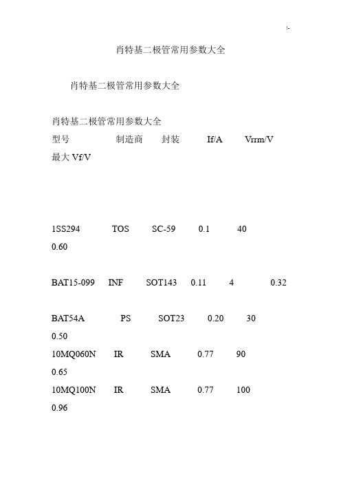
肖特基二极管常用参数大全肖特基二极管常用参数大全肖特基二极管常用参数大全型号制造商封装If/A Vrrm/V最大Vf/V1SS294 TOS SC-59 0.1 400.60BAT15-099 INF SOT143 0.11 4 0.32BAT54A PS SOT23 0.20 300.5010MQ060N IR SMA 0.77 900.6510MQ100N IR SMA 0.77 1000.9610BQ015 IR SMB 1.00 150.34SS12 GS DO214 1.00 20 0.50MBRS130LT3 ON - 1.00 300.3910BQ040 IR SMB 1.00 400.53RB060L-40 ROHM PMDS 1.00 400.55RB160L-40 ROHM PMDS 1.00 400.55SS14 GS DO214 1.00 40 0.50MBRS140T3 ON - 1.00 400.6010BQ060 IR SMB 1.00 600.57SS16 GS DO214 1.00 60 0.7510BQ100 IR SMB 1.00 100 0.78MBRS1100T3 ON - 1.00 100 0.7510MQ040N IR SMA 1.10 40 0.5115MQ040N IR SMA 1.70 40 0.55PBYR245CT PS SOT223 2.00 45 0.4530BQ015 IR SMC 3.00 15 0.3530BQ040 IR SMC 3.00 40 0.5130BQ060 IR SMC 3.00 60 0.5830BQ100 IR SMC 3.00 100 0.79STPS340U STM SOD6 3.00 400.84MBRS340T3 ON - 3.00 40 0.52RB051L-40 ROHM PMDS 3.00 40 0.45MBRS360T3 ON - 3.00 60 0.7030WQ04FN IR DPAK 3.30 40 0.6230WQ06FN IR DPAK 3.30 60 0.7030WQ10FN IR DPAK 3.30 100 0.9130WQ03FN IR DPAK 3.50 30 0.5250WQ03FN IR DPAK 5.50 30 0.5350WQ06FN IR DPAK 5.50 60 0.576CWQ06FN IR DPAK 6.60 600.586CWQ10FN IR DPAK pr 6.60 1000.811N5817 ON 轴向 1.00 20 0.75 1N5818 ON 轴向 1.00 30 0.55SB130 GS 轴向 1.00 30 0.50 1N5819 ON 轴向 1.00 40 0.60 MBR150 ON 轴向 1.00 501.00MBR160 ON 轴向 1.00 601.0011DQ10 IR 轴向 1.10 100 0.8511DQ04 IR 轴向 1.10 40 0.55 11DQ05 IR 轴向 1.10 50 0.58 11DQ06 IR 轴向 1.10 60 0.58MBRS340TR IR SMC 3.00 400.431N5820 ON 轴向 3.00 20 0.85 1N5821 ON 轴向 3.00 30 0.38 1N5822 ON 轴向 3.00 40 0.52MBR360 ON 轴向 3.00 601.00SS32 GS DO214 3.00 20 3.00 SS34 GS DO214 3.00 40 0.50 31DQ10 IR DO201 3.30 100 0.85SB530 GS 轴向 5.00 30 0.57 SB540 GS DO201 5.00 40 0.57 50SQ080 IR 轴向 5.00 80 0.66 50SQ100 IR 轴向 5.00 100 0.66 MBR735 GS TO220 7.50 350.84MBR745 GS TO220 7.50 450.84MBR745 IR TO220 7.50 450.8480SQ040 IR 轴向8.00 40 0.53 STQ080 IR TO220 8.00 80 0.72 8TQ100 TO220 8.00 100 0.72 80SQ040 IR 轴向8.00 40 0.5380SQ035 IR DO204AR 8.00 350.53HFA16PA60C IR TO247CT 8.00 6001.7095SQ015 轴向9.00 15 0.3190SQ040 轴向9.00 40 0.48 10TQ045 TO220 10.00 45 0.57 MBR1035 GS TO220 10.00 350.84MBR1045 ON TO220 10.00 450.84STPS1045F ON ISO220 10.00 45 0.64MBR2060CT ON TO220 10.00 600.85 <P style="TEXT-INDE。
MBR10200中文资料
0.5
A V/uS
0.85 0.71 0.1 6.0 200 2.0
1.05 -
V
IR
Cj RθJC TJ TSTG
0.009 10
mA mA pF ℃/W ℃ ℃
Operating Junction Temperature Range Storage Temperature Range Notes: 1. 2.0us Pulse Width, f=1.0 KHz 2. Pulse Test: 300us Pulse Width, 1% Duty Cycle 3. Mounted on Heatsink Size of 2 in x 3 in x 0.25in Al-Plate.
25
100 150
0.1
1
10 NUMBER OF CYCLES AT 60Hz
100
FIG.3- TYPICAL INSTANTANEOUS FORWARD CHARACTERISTICS
40
FIG.4- TYPICAL REVERSE CHARACTERISTICS
50 10
INSTANTANEOUS FORWARD CURRENT. (A)
PEAK FORWARD SURGE CURRENT. (A)
AVERAGE FORWARD CURRENT. (A)
RESISTIVE OR INDUCTIVE LOAD
10
150
8
125 100
6
75 50
4 2 0 0 50 CASE TEMPERATURE. ( C)
o
MBR1035-MBR1045 MBR1050-MBR10200
100
1,000
MBRB1045中文资料
MBRB1045中文资料MBRB1035 THRU MBRB1060SCHOTTKY RECTIFIERReverse Voltage -35 to 60 Volts Forward Current - 10.0 AmperesFEATURESFlammability Classifications 94V-0Metal silicon junction, majority carrier conductionLow power loss, high efficiency ?High current capability,low forward voltage drop ?High surge capabilityFor use in low voltage, high frequency inverters, freewheeling, and polarity protection applications ?Guardring for overvoltage protectionHigh temperature soldering in accordance with CECC 802 / Reflow guaranteedMECHANICAL DATACase:JEDEC TO-263AB molded plastic body Terminals:Leads solderable per MIL-STD-750, Method 2026Polarity:As marked Mounting Position:AnyWeight:0.08 ounces, 2.24 gramsMAXIMUM RATINGS AND ELECTRICAL CHARACTERISTICS Ratings at 25°C ambient temperature unless otherwise specified.SYMBOLSMBRB1035MBRB1045MBRB1050MBRB1060UNITSMaximum repetitive peak reverse voltage V RRM 35455060Volts Maximum working peak reverse voltage V RWM 35455060Volts Maximum DC blocking voltageV DC 35455060Volts Maximum average forward rectified current(SEE FIG.1)I (AV)10.0Amps Peak repetitive forward current at T C =135°C (square wave 20 KH Z)I FRM 20.0Amps Peak forward surge current8.3ms single half sine-wave superimposed on rated load (JEDEC Method)I FSM 150.0AmpsPeak repetitive reverse surge current (NOTE 1)I RRM 1.00.5Amps Voltage rate of change (rated V R )dv/dt 10,000V/μs Maximum instantaneous I F =10A, T C =25°C -0.80forward voltage at (NOTE 2)I F =10A, T C =125°C 0.570.70VoltsI F =20A, T C =25°C V F0.840.95I F =20A, T C =125°C0.720.85Maximum instantaneous reverse current at rated DC blocking voltage T C = 25°CI R 0.10mA (NOTE 2) T C =125°C 15.0Maximum thermal resistance, junction to case R ΘJC 2.0°C/W Operating junction temperature range T J -65 to +150°C Storage temperature rangeT STG-65 to +175°CNOTES:(1) 2.0μs pulse width, f=1.0 KH Z(2) Pulse test: 300μs pulse width, 1% duty cycle4/98TO-263AB。
MBR3045中文资料

Maximum Ratings
• •
Operating Temperature: -55°C to +150°C Storage Temperature: -55°C to +150°C Maximum Recurrent Peak Reverse Voltage 20V 30V 35V 40V 45V 60V 80V 100V Maximum DC Blocking Voltage 20V 30V 35V 40V 45V 60V 80V 100V
MBR3020 thru MBR30100
Figure 1 Typical Forward Characteristics 200 100 60 40 25 20 25°C Amps 10 6 4 2 1 .6 .4 .2 .1 0.05 0.06 0.07 Volts Instantaneous Forward Current - Amperes versus Instantaneous Forward Voltage - Volts 0.08 0.09 0.1 0 5 Amps 10 20 30
元器件交易网
MBR3020 thru MBR30100
Figure 4 Typical Reverse Characteristics 1000 600 400 350 200 100 60 40 20 mAmps 10 6 4 2 1 .6 .4 .2 .1 10 20 TA=25°C 40 60 Volts Instantaneous Reverse Leakage Current - MicroAmperes versus Percent Of Rated Peak Reverse Voltage - Volts 80 100 120 TA=125°C 0 1 2 4 Amps 300 250 200 100
日本三菱(RAYON)MBR帘式膜组件使用手册
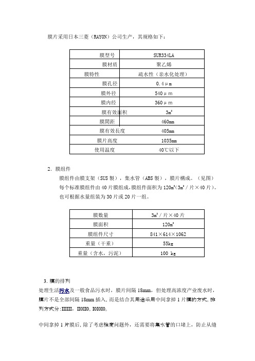
2.膜组件3.膜的排列处理生活污水及一般食品污水时,膜片间隔18mm,但处理高浓度产业废水时,膜片不是全部间隔18mm插入,而是结合其用途采用中间拿掉1片膜的方式。
排列方式分:IIIIII,II0II0,I0I0I0。
中间拿掉1片膜后,除了考虑強度问题外,还需要将集水管的口堵上,防止从缝隙处漏气。
现采用ABS隔板插入集水管部的方法。
二.设计基准1.原水适用于能够利用活性污泥法处理的排水。
原水中的有机物与通常的活性污泥法一样被微生物分解,再通过活性污泥槽中设置的膜,分离处理水和污泥。
①油分动植物油:80mg/l以下矿物油:3mg/l以下一般情况下,精密过滤膜上附有油脂成分(动植物油)时,油脂成分会覆盖膜表面,从而有可能堵塞微细孔,因此原水最好不要含有过多油脂成分。
设计原水超过80mg/l的情况下,需进行加压气浮、隔油等预处理,调整到80mg/l以下。
在含有矿物油的情况下,有可能对膜产生更恶劣的影响。
此时,进行预处理使n-Hex值降到3mg/l以下后,再使用膜分离活性污泥法。
②其他溶解在原水中的未被处理的有机物或未凝聚的絮凝剂吸附在膜表面时,会加快膜堵塞,妨碍稳定运转。
使用消泡剂进行消泡时不可使用硅类消泡剂,要使用乙醇类消泡剂,否则膜易堵塞。
升,膜压差上升后是否可以恢复。
2.预处理膜分离活性污泥法预处理的目的是用来除去可能给膜带来损伤的大的固态物,尤其是生活排水中包含的大量细小纤维屑、毛发等微小纤维状物质。
通常进入膜生物处理槽之前应经过开孔为Ф2mm的微细孔格栅过滤,对进行原水的预处理。
3.MBR生物反应槽设计①处理槽容量:按停留时间和BOD容积负荷分别计算,取最大值。
一般处理生活污水时,停留时间4小时以上BOD容积负荷:1.2Kg/m3.日当处理其他高浓度有机废水时,需经过实验确定各参数。
要求脱氮,脱磷时,除了考虑BOD外,还要考虑脱氮,脱磷所需的停留時間。
②活性污泥浓度采用膜分离活性污泥法,是用膜来进行固液分离,与通常的沉淀法不同MLSS能够保持高浓度。
肖特基二极管的参数
常用肖特基二极管参数型号制造商封装If/A Vrrm/V 最大Vf/V1SS294 TOS SC-59 0.1 40 0.60BAT15-099 INF SOT143 0.11 4 0.32BAT54A PS SOT23 0.20 30 0.5010MQ060N IR SMA 0.77 90 0.6510MQ100N IR SMA 0.77 100 0.9610BQ015 IR SMB 1.00 15 0.34SS12 GS DO214 1.00 20 0.50MBRS130LT3 ON - 1.00 30 0.3910BQ040 IR SMB 1.00 40 0.53RB060L-40 ROHM PMDS 1.00 40 0.55RB160L-40 ROHM PMDS 1.00 40 0.55 SS14 GS DO214 1.00 40 0.50MBRS140T3 ON - 1.00 40 0.6010BQ060 IR SMB 1.00 60 0.57SS16 GS DO214 1.00 60 0.7510BQ100 IR SMB 1.00 100 0.78MBRS1100T3 ON - 1.00 100 0.7510MQ040N IR SMA 1.10 40 0.5115MQ040N IR SMA 1.70 40 0.55PBYR245CT PS SOT223 2.00 45 0.45 30BQ015 IR SMC 3.00 15 0.3530BQ040 IR SMC 3.00 40 0.5130BQ060 IR SMC 3.00 60 0.58 30BQ100 IR SMC 3.00 100 0.79 STPS340U STM SOD6 3.00 40 0.84MBRS340T3 ON - 3.00 40 0.52 RB051L-40 ROHM PMDS 3.00 40 0.45 MBRS360T3 ON - 3.00 60 0.7030WQ04FN IR DPAK 3.30 40 0.62 30WQ06FN IR DPAK 3.30 60 0.70 30WQ10FN IR DPAK 3.30 100 0.9130WQ03FN IR DPAK 3.50 30 0.52 50WQ03FN IR DPAK 5.50 30 0.53 50WQ06FN IR DPAK 5.50 60 0.576CWQ06FN IR DPAK 6.60 60 0.586CWQ10FN IR DPAK pr 6.60 100 0.81 1N5817 ON 轴向 1.00 20 0.75 1N5818 ON 轴向 1.00 30 0.55 SB130 GS 轴向 1.00 30 0.501N5819 ON 轴向 1.00 40 0.60MBR150 ON 轴向 1.00 50 1.00MBR160 ON 轴向 1.00 60 1.0011DQ10 IR 轴向 1.10 100 0.8511DQ04 IR 轴向 1.10 40 0.5511DQ05 IR 轴向 1.10 50 0.58MBRS340TR IR SMC 3.00 40 0.431N5820 ON 轴向 3.00 20 0.851N5821 ON 轴向 3.00 30 0.381N5822 ON 轴向 3.00 40 0.52MBR360 ON 轴向 3.00 60 1.00SS32 GS DO214 3.00 20 3.00SS34 GS DO214 3.00 40 0.50 31DQ10 IR DO201 3.30 100 0.85SB530 GS 轴向 5.00 30 0.57 SB540 GS DO201 5.00 40 0.57 50SQ080 IR 轴向 5.00 80 0.6650SQ100 IR 轴向 5.00 100 0.66MBR735 GS TO220 7.50 35 0.84 MBR745 GS TO220 7.50 45 0.84 MBR745 IR TO220 7.50 45 0.8480SQ040 IR 轴向8.00 40 0.53STQ080 IR TO220 8.00 80 0.728TQ100 TO220 8.00 100 0.7280SQ040 IR 轴向8.00 40 0.5380SQ035 IR DO204AR 8.00 35 0.53 HFA16PA60C IR TO247CT 8.00 600 1.7095SQ015 轴向9.00 15 0.3110TQ045 TO220 10.00 45 0.57 MBR1035 GS TO220 10.00 35 0.84 MBR1045 ON TO220 10.00 45 0.84 STPS1045F ON ISO220 10.00 45 0.64MBR2060CT ON TO220 10.00 60 0.85MBR1060 ON TO220 10.00 60 0.95 PBYR10100 PS TO220 10.00 100 0.7010TQ040 IR TO220 10.00 40 0.57MBR1045 IR TO220 10.00 45 0.8410CTQ150-1 IR D2pak 10.00 150 0.7340L15CTS IR D2pak 10.00 150 0.4185CNQ015A IR D61 80.00 15 0.32150K40A IR D08 150.00 400 1.3312CTQ040 IR TO220 12.00 45 0.73MBR1545CT IR TO220 pr 15.00 45 0.72MBR1660 GS TO220 16.00 60 0.75 16CTQ080 IR TO220 pr 16.00 80 0.72 16CTQ100 IR TO220 pr 16.00 100 0.72 16CTQ100-1 IR D2Pak 16.00 100 0.7218TQ045 ON TO220 18.00 45 0.60HFA16PB120 IR TO247 16.00 1200 3.00 MBR1645 IR TO220AC 16.00 45 0.63 19CTQ015 IR TO220 19.00 15 0.3620CTQ045 IR TO220 pr 20.00 45 0.64 20TQ045 IR TO220 20.00 45 0.57 MBR2045CT IR TO220 pr 20.00 45 0.84MBR2090CT IR TO220 pr 20.00 90 0.80 MBR20100CT IR TO220 pr 20.00 100 0.80MBR20100CT-1IR TO262 20.00 100 0.80 MBR2080CT IR TO220AB 20.00 80 0.85 MBR2545CT IR TO220AB 30.00 45 0.82 MBR3045WT IR TO247 30.00 4532CTQ030 IR TO220 pr 30.00 30 0.49 32CTQ303-1 IR D2Pak 30.00 30 0.49 30CPQ060 IR TO220 pr 30.00 60 0.62 30CPQ080 IR TO247AC 30.00 80 0.86 30CPQ100 IR TO247 pr 30.00 100 0.86 30CPQ150 IR TO247 pr 30.00 150 1.00 40CPQ040 IR TO247 pr 40.00 40 0.49 40CPQ045 IR TO247 pr 40.00 45 0.49 40CPQ050 IR TO247AA 40.00 50 0.53 40CPQ100 IR TO247 pr 40.00 100 0.77 40L15CT IR TO220AB 40.00 15 0.53 47CTQ020 IR TO220 40.00 20 0.34 48CTQ060 IR TO220 40.00 60 0.5840L15CW IR TO247 40.00 15 0.5242CTQ030 IR TO220 40.00 30 0.38 40CTQ045 IR TO220 40.00 45 0.6840L45CW IR TO247 40.00 45 0.7040CPQ060 ON TO247 40.00 60 0.68 MBR4045WT IR TO247 40.00 45 0.59 MBR4060WT IR TO247 40.00 60 0.77 43CTQ100 IR TO220 40.00 100 0.9852CPQ030 IR TO247 50.00 30 0.38MBR6045WT IR TO247pr 60.00 45 0.73STPS6045CPI ON TOP3I 60.00 45 0.8465PQ015 IR TO247 65.00 15 0.5072CPQ030 IR TO247AC 70.00 30 0.5185CNQ015 IR D61 80.00 15 0.3283CNQ100 IR D61 80.00 100 0.6780CPQ020 IR TO247 80.00 20 0.3282CNQ030A IR D61 80.00 30 0.3782CNQ045A IR D61 80.00 45 0.4783CNQ100A IR D61 80.00 100 0.67120NQ045 IR HALFPAK 120.00 45 0.52125NQ015 IR D67 120.00 15 0.33122NQ030 IR D67 120.00 30 0.41 STPS16045TV ON ISOTOP 160.00 45 0.95 182NQ030 IR D67 180.00 30 0.41200CNQ040 IR TO244AB 200.00 40 0.54200CNQ045 IR TO244AB 200.00 45 0.54200CNQ030 IR TO244AB 200.00 30 0.48STPS24045TV ON ISOTOP 240.00 45 0.91203CMQ080 IR TO244 200.00 80 1.03240NQ045 IR HALFPAK 240.00 45 0.55301CNQ045 IR TO244 300.00 45 0.59403CNQ100 IR TO244AB 400.00 100 0.83440CNQ030 IR TO244AB 440.00 30 0.41系统分类: 电源技术 | 用户分类: 电源技术 |。
材料1035
材料1035材料1035是一种新型的复合材料,具有轻质、高强度、耐腐蚀等优点,被广泛应用于航空航天、汽车制造、建筑材料等领域。
本文将对材料1035的特性、应用和发展前景进行介绍。
首先,材料1035具有轻质高强度的特点。
它由多种材料复合而成,具有优异的机械性能,同时重量轻,密度小,可以大幅减轻产品的重量,提高产品的使用寿命。
这使得材料1035在航空航天领域得到了广泛的应用,例如飞机机身、发动机零部件等都可以采用材料1035制造,大大提高了飞行器的性能和安全性。
其次,材料1035具有良好的耐腐蚀性能。
在恶劣的环境下,材料1035能够保持稳定的性能,不易受到外界环境的影响,具有较长的使用寿命。
因此,汽车制造领域也广泛采用材料1035,例如汽车车身、底盘等部件都可以采用材料1035,提高了汽车的耐用性和安全性。
此外,材料1035还具有良好的加工性能和成型性能,可以满足不同领域的加工需求,为产品的设计和制造提供了更多可能性。
因此,建筑材料领域也开始逐渐采用材料1035,例如钢结构、桥梁等都可以采用材料1035,提高了建筑物的强度和稳定性。
随着科技的不断进步,材料1035的研发和应用也在不断推进。
未来,随着材料1035的性能不断提升和成本的进一步降低,它将会在更多领域得到广泛的应用,为人类的生产生活带来更多的便利和改善。
综上所述,材料1035具有轻质高强度、耐腐蚀、良好的加工性能和成型性能等优点,被广泛应用于航空航天、汽车制造、建筑材料等领域,并且在未来有着广阔的发展前景。
相信随着科技的不断进步,材料1035将会为人类社会的发展做出更大的贡献。
- 1、下载文档前请自行甄别文档内容的完整性,平台不提供额外的编辑、内容补充、找答案等附加服务。
- 2、"仅部分预览"的文档,不可在线预览部分如存在完整性等问题,可反馈申请退款(可完整预览的文档不适用该条件!)。
- 3、如文档侵犯您的权益,请联系客服反馈,我们会尽快为您处理(人工客服工作时间:9:00-18:30)。
SQUARE WAVE
dc
IF(AV) , AVERAGE FORWARD CURRENT (AMPS)
10
5.0 RATED VOLTAGE APPLIED RqJA = 60°C/W I I 3.0
4.0
(CAPACITIVE LOAD) PK I 6.0 AV 5.0 4.0 3.0 2.0 1.0 0 0 2.0 4.0 6.0 20 10
PK AV
+ p (RESISTIVE LOAD)
PK 10 (CAPACITIVE LOAD) I AV
5.0
+5
10 20
dc
0 110 120 130 140 150 160 TC, CASE TEMPERATURE (°C)
AV
+ 20, 10, 5
80 100 120 140 160
60
TA, AMBIENT TEMPERATURE (°C)
元器件交易网MOTORFra bibliotekLASEMICONDUCTOR TECHNICAL DATA
Order this document by MBR1035/D
SWITCHMODE™ Power Rectifiers
. . . using the Schottky Barrier principle with a platinum barrier metal. These state–of–the–art devices have the following features: • • • • • Guardring for Stress Protection Low Forward Voltage 150°C Operating Junction Temperature Guaranteed Reverse Avalanche Epoxy Meets UL94, VO at 1/8″
TIME t1 ∆TJL = Ppk • RθJL [D + (1 – D) • r(t1 + tp) + r(tp) – r(t1)] where: ∆TJL = the increase in junction temperature above the lead temperature. r(t) = normalized value of transient thermal resistance at time, t, i.e.: r(t1 + tp) = normalized value of transient thermal resistance at time, t1 + tp. 10 100 1000
©RectifierInc. 1996 Data Motorola, Device
1
元器件交易网 MBR1035 MBR1045
100 70 50 TJ = 150°C 100°C 25°C 100 TJ = 150°C 70 25°C 50 100°C
30 20 iF, INSTANTANEOUS FORWARD CURRENT (AMPS) iF, INSTANTANEOUS FORWARD CURRENT (AMPS) 0.2 0.4 0.6 0.8 1.0 1.4
30 20
10 7.0 5.0 3.0 2.0
10 7.0 5.0 3.0 2.0
1.0 0.7 0.5 0.3 0.2
1.0 0.7 0.5 0.3 0.2
0.1 1.2 vF, INSTANTANEOUS VOLTAGE (VOLTS)
0.1 0.2 0.4 0.6 0.8 1.0 1.2 1.4 vF, INSTANTANEOUS VOLTAGE (VOLTS)
Figure 5. Current Derating, Infinite Heatsink
PF(AV) , AVERAGE FORWARD POWER DISSIPATION (WATTS)
Figure 6. Current Derating, RqJA = 16°C/W
9.0 8.0 7.0 I
SINE WAVE RESISTIVE LOAD
MBR1035 MBR1045
MBR1045 is a Motorola Preferred Device
Mechanical Characteristics: • Case: Epoxy, Molded • Weight: 1.9 grams (approximately) • Finish: All External Surfaces Corrosion Resistant and Terminal Leads are Readily Solderable • Lead Temperature for Soldering Purposes: 260°C Max. for 10 Seconds • Shipped 50 units per plastic tube • Marking: B1035, B1045
MBR1035 MBR1045
RATED VOLTAGE APPLIED 14 I 12 10 8.0 6.0 dc 4.0 2.0 0 0 20 40 I (CAPACITIVE LOAD) PK I SQUARE WAVE I
PK AV
+ p (RESISTIVE LOAD)
SQUARE WAVE
200
100 70 50
30 20 1.0 2.0 3.0 5.0 7.0 10 20 30 50 70 100 NUMBER OF CYCLES AT 60 Hz
Figure 3. Maximum Reverse Current
Figure 4. Maximum Surge Capability
2
Preferred devices are Motorola recommended choices for future use and best overall value.
vF 0.57 0.72 0.84 iR 15 0.1 15 0.1 0.57 0.72 0.84
Volts
mA
Rev 2
ELECTRICAL CHARACTERISTICS
Maximum Instantaneous Forward Voltage (1) (iF = 10 Amps, TC = 125°C) (iF = 20 Amps, TC = 125°C) (iF = 20 Amps, TC = 25°C) Maximum Instantaneous Reverse Current (1) (Rated dc Voltage, TC = 125°C) (Rated dc Voltage, TC = 25°C) (1) Pulse Test: Pulse Width = 300 µs, Duty Cycle ≤ 2.0%. SWITCHMODE is a trademark of Motorola, Inc.
+5
PK AV
+ p (RESISTIVE LOAD)
SQUARE WAVE
2.0 dc 1.0 0 0 20 40 (CAPACITIVE LOAD) PK I I
TJ = 150°C
AV
60
+ 20, 10, 5
80 100 120 140 160
8.0
10
12
14
16
IF(AV), AVERAGE FORWARD CURRENT (AMPS)
3 1, 4
SCHOTTKY BARRIER RECTIFIERS 10 AMPERES 20 to 45 VOLTS
4
1 3
CASE 221B–03 TO–220AC PLASTIC
MAXIMUM RATINGS
Rating Peak Repetitive Reverse Voltage Working Peak Reverse Voltage DC Blocking Voltage Average Rectified Forward Current (Rated VR) TC = 135°C Peak Repetitive Forward Current (Rated VR, Square Wave, 20 kHz) TC = 135°C Nonrepetitive Peak Surge Current (Surge applied at rated load conditions halfwave, single phase, 60 Hz) Peak Repetitive Reverse Surge Current (2.0 µs, 1.0 kHz) See Figure 12 Operating Junction Temperature Storage Temperature Voltage Rate of Change (Rated VR) Symbol VRRM VRWM VR IF(AV) IFRM IFSM IRRM TJ Tstg dv/dt MBR1035 35 MBR1045 45 Unit Volts
TA, AMBIENT TEMPERATURE (°C)
Figure 7. Forward Power Dissipation
Figure 8. Current Derating, Free Air
r(t), TRANSIENT THERMAL RESISTANCE (NORMALIZED)
1.0 0.7 0.5 0.3 0.2 tp 0.1 0.07 0.05 0.03 0.02 0.01 0.01 0.1 1.0 t, TIME (ms) Ppk Ppk DUTY CYCLE, D = tp/t1 PEAK POWER, Ppk, is peak of an equivalent square power pulse.