ad549中文资料
ad549中文资料

极低偏置电流运算放大器AD5491 概述AD549是具有极低输入偏置电流的单片电路静电计型运算放大器。
为达到高精度的目的,输入偏置电压和输入偏置电压漂移均通过激光调节。
这种极低输入电流性能由ADI公司专有的topgate工艺技术完成。
该技术可以制造与具有极低输入电流的JFET并与双极性电路隔离的集成运放。
输入级具有1015Ω的共模阻抗,其输入电流与共模电压无关。
AD549适用于低输入电流和低输入偏置电压的场合。
它特别适合用作各种电流输出的传感器,如光电二极管、光电倍增管以及氧气传感器等的前置放大器。
该产品也可用作精密积分器或低衰减采样保持器。
AD549的封装与标准FET和静电计运算放大器兼容,因此用户花少量成本即可对系统升级,提高已有系统的性能。
AD549有TO-99密封封装。
金属外壳与8管脚相连,使得金属外壳与同样电压的输入终端独立连接,达到降低外壳泄漏的目的。
AD549具有四种性能等级。
其中J、K和L型号的温度范围是0℃到70℃。
S型号专用于军事,其温度范围:-55℃到125℃。
AD549的输入电流在整个共模输入电压范围内都得到保证,其输入失调电压和漂移由激光分别调节到0.25mV和5μV/℃(AD549K);1mV和20μV/℃(AD549J)。
700μA的最大静态电流使输入电流和偏置电压的热效应降到最低。
模拟性能包括1MHz的均匀增益带宽和3V/μs的压摆率。
当输入为10V时,建立时间是5μs 到0.01%。
2 AD549的引脚及特性参数图一所示是AD549的引脚图,表一所示是其特性参数。
图一AD549引脚图表一AD549的主要特性nV/ nV/ nV/ nV/fA/3 AD549的工作原理3.1 最小化输入电流AD549具有很小的输入电流和失调电压。
在实际应用中应谨慎考虑如何使用放大器可以减小输入电流。
为减小输入电流,该放大器的工作温度应尽可能低。
像其他JFET输入放大器一样,AD549的输入电流对芯片温度很敏感,上升斜率因子为每10℃的2.3。
AD5447资料

Dual 8-,10-,12-Bit High BandwidthMultiplying DACs with Serial InterfaceAD5429/AD5439/AD5449 Rev.0Information furnished by Analog Devices is believed to be accurate and reliable.However, no responsibility is assumed by Analog Devices for its use, nor for anyinfringements of patents or other rights of third parties that may result from its use. Specifications subject to change without notice. No license is granted by implication or otherwise under any patent or patent rights of Analog Devices. Trademarks and registered trademarks are the property of their respective owners.One Technology Way, P.O. Box 9106, Norwood, MA 02062-9106, U.S.A. Tel: Fax: 781.326.8703© 2004 Analog Devices, Inc. All rights reserved.FEATURES10 MHz multiplying bandwidth50 MHz serial interface2.5 V to 5.5 V supply operation±10 V reference inputPin compatible 8-, 10-, and 12-bit DACs Extended temperature range: −40°C to +125°C 16-lead TSSOP packageGuaranteed monotonicPower-on resetDaisy-chain modeReadback function0.5 µA typical current consumption APPLICATIONSPortable battery-powered applications Waveform generatorsAnalog processingInstrumentation applications Programmable amplifiers and attenuators Digitally controlled calibration Programmable filters and oscillators Composite videoUltrasoundGain, offset, and voltage trimmingFUNCTIONAL BLOCK DIAGRAMSYNCSCLKSDINI OUT1BI OUT1AR FB AI OUT2AI OUT2B4464--1V DDR FB BSDOFigure 1.GENERAL DESCRIPTIONThe AD5429/AD5439/AD54491 are CMOS 8-, 10-, and 12-bit dual-channel current output digital-to-analog converters, respectively. These devices operate from a 2.5 V to 5.5 V power supply, making them suited to battery-powered and other applications.The applied external reference input voltage (V REF) determines the full-scale output current. An integrated feedback resistor (R FB) provides temperature tracking and full-scale voltage output when combined with an external current-to-voltage precision amplifier.These DACs utilize a double-buffered, 3-wire serial interface that is compatible with SPI®, QSPI™, MICROWIRE™, and most DSP interface standards. In addition, a serial data out pin (SDO) allows daisy-chaining when multiple packages are used. Data readback allows the user to read the contents of the DAC register via the SDO pin. On power-up, the internal shift register and latches are filled with zeros and the DAC outputs are at zero scale.As a result of manufacture on a CMOS submicron process, these parts offer excellent 4-quadrant multiplication character-istics, with large signal multiplying bandwidths of 10 MHz. The AD5429/AD5439/AD5449 DAC are available in 16-lead TSSOP packages.1 US Patent Number 5,689,257.AD5429/AD5439/AD5449Rev. 0 | Page 2 of 32TABLE OF CONTENTSSpecifications.....................................................................................3 Timing Characteristics.....................................................................5 Absolute Maximum Ratings............................................................7 ESD Caution..................................................................................7 Pin Configuration and Function Descriptions.............................8 Terminology......................................................................................9 Typical Performance Characteristics...........................................10 General Description.......................................................................15 Unipolar Mode............................................................................15 Bipolar Operation.......................................................................16 Stability........................................................................................16 Single-Supply Applications........................................................17 Positive Output Voltage.............................................................17 Adding Gain................................................................................18 Divider or Programmable Gain Element................................18 Reference Selection....................................................................19 Amplifier Selection....................................................................19 Serial Interface................................................................................20 Microprocessor Interfacing.......................................................22 PCB Layout and Power Supply Decoupling................................24 Power Supplies for the Evaluation Board................................24 Evaluation Board for the DACs................................................24 Overview of AD54xx Devices.......................................................28 Outline Dimensions.......................................................................29 Ordering Guide.. (29)REVISION HISTORY7/04—Revision 0: Initial VersionAD5429/AD5439/AD5449SPECIFICATIONSV DD = 2.5 V to 5.5 V, V REF = 10 V, I OUT2A, I OUT2B = 0 V. All specifications T MIN to T MAX, unless otherwise noted. DC performance measured with OP1177, ac performance with AD9631, unless otherwise noted. Temperature range for Y version is −40°C to +125°C.Table 1.Parameter Min Typ Max Unit ConditionsSTATIC PERFORMANCEAD5429Resolution 8 BitsRelative Accuracy ±0.5 LSBDifferential Nonlinearity ±1 LSB Guaranteed monotonicAD5439Resolution 10 BitsRelative Accuracy ±0.5 LSBDifferential Nonlinearity ±1 LSB Guaranteed monotonicAD5449Resolution 12 BitsRelative Accuracy ±1 LSBDifferential Nonlinearity −1/+2 LSB Guaranteed monotonicGain Error ±10 mVGain Error Temp Coefficient1±5 ppm FSR/°COutput Leakage Current ±5 nA Data = 0000H, T A = 25°C, I OUT1±10 nA Data = 0000H, I OUT1REFERENCE INPUT1Typical resistor TC = −50 ppm/°C Reference Input Range ±10 VV REF A,V REF B Input Resistance 8 10 12 kΩ DAC input resistanceV REF A/B Input Resistance Mismatch 1.6 2.5 % Typ = 25°C, max = 125°CDIGITAL INPUTS/OUTPUT1Input High Voltage, V IH 1.7 V V DD = 2.5 V to 5.5 VInput Low Voltage, V IL0.8 V V DD = 2.7 V to 5.5 V0.7 V V DD = 2.5 V to 2.7 VInput Leakage Current, I IL 1 µAInput Capacitance 10 pFV DD = 4.5 V to 5.5 VOutput Low Voltage, V OL0.4 V I SINK = 200 µAOutput High Voltage, V OH V DD − 1 V I SOURCE = 200 µAV DD = 2.5 V to 3.6 VOutput Low Voltage, V OL0.4 V I SINK = 200 µAOutput High Voltage, V OH V DD − 0.5 V I SOURCE = 200 µADYNAMIC PERFORMANCE1Reference Multiplying BW 10 MHz V REF = 5 V p-p, DAC loaded all 1sOutput Voltage Settling Time Measured to ±4 mV of FS, R LOAD = 100 Ω,C LOAD = 0sAD5429 50 100 nsAD5439 55 110 ns DAC latch alternately loaded with 0sand 1sAD5449 90 160 ns R LOAD = 100 Ω, C LOAD = 15 pFDigital Delay 20 40 nsDigital-to-Analog Glitch Impulse 3 nV-s 1 LSB change around major carry,V REF = 0 VMultiplying Feedthrough Error −75 dB DAC latch loaded with all 0s,reference = 10 kHzRev. 0 | Page 3 of 32AD5429/AD5439/AD5449Rev. 0 | Page 4 of 32ParameterMin Typ Max Unit ConditionsOutput Capacitance 2 pF DAC latches loaded with all 0s4 pF DAC latches loaded with all 1sDigital Feedthrough 5 nV-sFeedthrough to DAC output with CS high and alternate loading of all 0s and all 1s Total Harmonic Distortion −75 dB V REF = 5 V p-p, all 1s loaded, f = 1 kHz−75 dBV REF = 5 V, sine wave generated from digital code Output Noise Spectral Density 25 nV/√Hz@ 1 kHzSFDR PERFORMANCE (Wideband) AD5449, 65 k codes, V REF = 3.5 V Clock = 10 MHz 500 kHz fout 55 dB 100 kHz fout 63 dB 50 kHz fout 65 dB Clock = 25 MHz 500 kHz fout 50 dB 100 kHz fout 60 dB 50 kHz fout 62 dBSFDR PERFORMANCE (Narrow Band) AD5449, 65 k codes, V REF = 3.5 V Clock = 10 MHz 500 kHz fout 73 dB 100 kHz fout 80 dB 50 kHz fout 87 dB Clock = 25 MHz 500 kHz fout 70 dB 100 kHz fout 75 dB 50 kHz fout 80 dBINTERMODULATION DISTORTION AD5449, 65 k codes, V REF = 3.5 V Clock = 10 MHz f 1 = 400 kHz, f 2 = 500 kHz 65 dB f 1 = 40 kHz, f 2 = 50 kHz 72 dB Clock = 25 MHz f 1 = 400 kHz, f 2 = 500 kHz 51 dB f 1 = 40 kHz, f 2 = 50 kHz 65 dB POWER REQUIREMENTS Power Supply Range 2.5 5.5 VI DD 10 µALogic inputs = 0 V or V DD Power Supply Sensitivity 10.001 %/%∆V DD = ±5%1Guaranteed by design and characterization, not subject to production test.AD5429/AD5439/AD5449TIMING CHARACTERISTICSV DD = 2.5 V to 5.5 V, V REF = 5 V, I OUT2 = 0 V. All specifications T MIN to T MAX, unless otherwise noted.See Figure 2 and Figure 3. Temperature range for Y version is −40°C to +125°C. Guaranteed by design and characterization, not subject to production test. All input signals are specified with tr = tf = ns (10% to 90% of V DD) and timed from a voltage level of (V IL + V IH)/2.1 Falling or rising edge as determined by the control bits of the serial word. Strong or weak SDO driver selected via the control register.2 Daisy-chain and readback modes cannot operate at maximum clock frequency. SDO timing specifications are measured with a load circuit, as shown in Figure 4.Rev. 0 | Page 5 of 32AD5429/AD5439/AD5449Rev. 0 | Page 6 of 32SCLKDINLDAC 12NOTES1ASYNCHRONOUS LDAC UPDATE MODE 2ALTERNATIVELY, DATA CAN BE CLOCKED INTO INPUT SHIFT REGISTER ON RISING EDGE OF SCLK AS DETERMINED BY CONTROL BITS. TIMING AS ABOVE, WITH SCLK INVERTED.04464-0-002Figure 2. Standalone Mode Timing Diagram04464-0-003SCLKSYNCSDINSDOALTERNATIVELY, DATA CAN BE CLOCKED INTO INPUT SHIFT REGISTER ON RISING EDGE OF SCLK AS DETERMINED BY CONTROL BITS. IN THIS CASE, DATA WOULD BE CLOCKED OUT OF SDO ON FALLING EDGE OF SCLK. TIMING AS ABOVE, WITH SCLK INVERTED.Figure 3. Daisy-Chain and Readback Modes Timing DiagramPINFigure 4. Load Circuit for SDO Timing SpecificationsAD5429/AD5439/AD5449Rev. 0 | Page 7 of 32ABSOLUTE MAXIMUM RATINGSTable 3.Parameter RatingV DD to GND −0.3 V to +7 VV REF , R FB to GND −12 V to +12 VI OUT 1, I OUT 2 to GND −0.3 V to +7 VInput Current to Any Pin except Supplies ±10 mALogic Inputs and Output 1−0.3 V to V DD + 0.3 VOperating Temperature RangeExtended (Y Version)−40°C to +125°C Storage Temperature Range −65°C to +150°C Junction Temperature150°C 16-Lead TSSOP θJA Thermal Impedance 150°C/W Lead Temperature, Soldering (10 s) 300°C IR Reflow, Peak Temperature (< 20 s)235°C1Overvoltages at SCLK, SYNC , and DIN are clamped by internal diodes. Current should be limited to the maximum ratings given.Stresses above those listed under Absolute Maximum Ratings may cause permanent damage to the device. This is a stress rating only; functional operation of the device at these or any other conditions above those listed in the operational sections of this specification is not implied. Exposure to absolute maximum rating conditions for extended periods may affect device reliability. Only one absolute maximum rating may be applied at any one time. Transient currents of up to 100 mA do not cause SCR latch-up. T A = 25°C unless otherwise noted.ESD CAUTIONESD (electrostatic discharge) sensitive device. Electrostatic charges as high as 4000 V readily accumulate on the human body and test equipment and can discharge without detection. Although this product features proprietary ESD protection circuitry, permanent damage may occur on devices subjected to high energy electrostatic discharges. Therefore, proper ESD precautions are recommended to avoid performancedegradation or loss of functionality.AD5429/AD5439/AD5449Rev. 0 | Page 8 of 32PIN CONFIGURATION AND FUNCTION DESCRIPTIONSNC = NO CONNECT04464-0-005Figure 5. Pin ConfigurationAD5429/AD5439/AD5449Rev. 0 | Page 9 of 32TERMINOLOGYRelative AccuracyRelative accuracy or endpoint nonlinearity is a measure of the maximum deviation from a straight line passing through the endpoints of the DAC transfer function. It is measured after adjusting for zero and full scale and is typically expressed in LSBs or as a percentage of full-scale reading.Differential NonlinearityDifferential nonlinearity is the difference between the measured change and the ideal 1 LSB change between any two adjacent codes. A specified differential nonlinearity of ±1 LSB maximum over the operating temperature range ensures monotonicity. Gain ErrorGain error or full-scale error is a measure of the output error between an ideal DAC and the actual device output. For these DACs, ideal maximum output is V REF − 1 LSB. Gain error of the DACs is adjustable to zero with external resistance.Output Leakage CurrentOutput leakage current is current that flows in the DAC ladder switches when these are turned off. For the I OUT 1 terminal, it can be measured by loading all 0s to the DAC and measuring the I OUT 1 current. Minimum current flows in the I OUT 2 line when the DAC is loaded with all 1s.Output CapacitanceCapacitance from I OUT 1 or I OUT 2 to AGND.Output Current Settling TimeThe amount of time needed for the output to settle to aspecified level for a full-scale input change. For these devices, it is specified with a 100 Ω resistor to ground.Digital-to-Analog Glitch lmpulseThe amount of charge injected from the digital inputs to the analog output when the inputs change state. This is normally specified as the area of the glitch in either pA-s or nV-s,depending upon whether the glitch is measured as a current or voltage signal.Digital FeedthroughWhen the device is not selected, high frequency logic activity on the device digital inputs is capacitively coupled through the device to show up as noise on the I OUT pins and subsequently into the following circuitry. This noise is digital feedthrough. Multiplying Feedthrough ErrorThe error due to capacitive feedthrough from the DAC reference input to the DAC I OUT 1 terminal, when all 0s are loaded to the DAC.Digital CrosstalkThe glitch impulse transferred to the outputs of one DAC in response to a full-scale code change (all 0s to all 1s and vice versa) in the input register of the other DAC. It is expressed in nV-s.Analog CrosstalkThe glitch impulse transferred to the output of one DAC due to a change in the output of another DAC. It is measured byloading one of the input registers with a full-scale code change (all 0s to all 1s and vice versa), while keeping LDAC high. Then pulse LDAC low and monitor the output of the DAC whose digital code was not changed. The area of the glitch is expressed in nV-s.Channel-to-Channel IsolationThe proportion of input signal from the reference input of one DAC that appears at the output of the other DAC. It is expressed in dB.Total Harmonic Distortion (THD)The DAC is driven by an ac reference. The ratio of the rms sum of the harmonics of the DAC output to the fundamental value is the THD. Usually only the lower-order harmonics are included, such as second to fifth.()125242322log20V V V V V THD +++=Intermodulation DistortionThe DAC is driven by two combined sine wave references of frequencies fa and fb. Distortion products are produced at sum and difference frequencies of mfa ± nfb, where m,n = 0, 1, 2, 3… Intermodulation terms are those for which m or n is not equal to zero. The second-order terms include (fa + fb) and (fa − fb) and the third-order terms are (2fa + fb), (2fa − fb), (f + 2fa + 2fb) and (fa − 2fb). IMD is defined as()lfundamenta the of amplitude rms products distortion diff and sum the of sum rms IMD log20=Compliance Voltage RangeThe maximum range of (output) terminal voltage for which the device provides the specified characteristics.AD5429/AD5439/AD5449Rev. 0 | Page 10 of 32TYPICAL PERFORMANCE CHARACTERISTICS–0.20–0.15–0.10–0.0500.05I N L (L S B )0.100.150.2004462-0-007050100150200250CODEFigure 6. INL vs. Code (8-Bit DAC)–0.5–0.4–0.3–0.2–0.100.10.20.30.40.5I N L (L S B )04462-0-0082004006008001000CODEFigure 7. INL vs. Code (10-Bit DAC)–1.0–0.8–0.6–0.4–0.200.20.40.60.81.0I N L (L S B )2000150050010002500300035004000CODE04462-0-009Figure 8. INL vs. Code (12-Bit DAC) –0.20–0.15–0.10–0.0500.05D N L (L S B )0.100.150.2004462-0-010050100150200250CODEFigure 9. DNL vs. Code (8-Bit DAC)–0.5–0.4–0.3–0.2–0.100.10.20.30.40.5D N L (L S B )04462-0-01102004006008001000CODEFigure 10. DNL vs. Code (10-Bit DAC)–1.0–0.8–0.6–0.4–0.200.20.40.60.81.0D N L (L S B )2000150050010002500300035004000CODE04462-0-012Figure 11. DNL vs. Code (12-Bit DAC)–0.3–0.2–0.100.10.20.30.40.50.6I N L (L S B )65342789REFERENCE VOLTAGE04462-0-01310Figure 12. INL vs. Reference Voltage–0.70–0.65–0.60–0.55–0.50–0.45–0.40D N L (L S B )65342789REFERENCE VOLTAGE04462-0-01410Figure 13. DNL vs. Reference Voltage–5–4–3–2–1012345E R R O R (m V )–60–40–20020406080100120140TEMPERATURE (°C)04462-0-015Figure 14. Gain Error vs. TemperatureINPUT VOLTAGE (V)C U R R E N T (m A )850 5.0763142 4.54.03.53.02.52.01.51.00.504462-0-022Figure 15. Supply Current vs. Logic Input Voltage00.20.40.60.81.0I O U T L E A K A G E (n A )1.21.41.6TEMPERATURE (°C)04462-0-023Figure 16. I OUT 1 Leakage Current vs. Temperature00.050.100.150.200.250.300.350.400.450.50C U R R E N T (µA )–60–40–20020406080100120140TEMPERATURE (°C)04462-0-024Figure 17. Supply Current vs. Temperature2468101214I D D (m A )10k 1k 101001100k 1M 10M 100MFREQUENCY (Hz)04462-0-025Figure 18. Supply Current vs. Update Rate–102–66–54–42–30–18–6611001k 10k 100k 1M10M100MFREQUENCY (Hz)G A I N (d B )0–60–48–36–24–12–84–72–78–90–9604462-0-02610Figure 19. Reference Multiplying Bandwidth vs. Frequency and Code–0.8–0.6–0.4–0.20.2G A I N (d B )10k 1k 101001100k 1M 10M 100M FREQUENCY (Hz)04462-0-027Figure 20. Reference Multiplying Bandwidth–All 1s Loaded–9–6–3310k100k1M10M100MFREQUENCY (Hz)G A I N (d B )04462-0-028Figure 21. Reference Multiplying Bandwidth vs. Frequency andCompensation Capacitor–0.010–0.0050.0050.0250.0350.0450.01500.0200.0300.0400.010O U T P U T V O L T A G E (V )20406080100120140160180200TIME (ns)04462-0-041Figure 22. Midscale Transition, V REF = 0 VO U T P U T V O L T A G E (V )020406080100120140160180200TIME (ns)04462-0-042–1.77–1.76–1.75–1.74–1.73–1.72–1.71–1.70–1.69–1.68Figure 23. Midscale Transition, V REF = 3.5 V–120–100–80–60020FREQUENCY (Hz)–40–20P S R R (d B )04462-0-04310Figure 24. Power Supply Rejection vs. Frequency–90–85–80–75–70–65–60T H D + N (d B )1001k11010k100k1MFREQUENCY (Hz)04462-0-044Figure 25. THD + Noise vs. Frequency20406080100S F D R (d B )020406080100120140160180200f OUT (kHz)04462-0-045Figure 26. Wideband SFDR vs. f OUT Frequency102030405060708090S F D R (d B )1002003004005006007008009001000f OUT (kHz)04462-0-046Figure 27. Wideband SFDR vs. f OUT Frequency04462-0-047–90–70–50–30–10S F D R (d B )FREQUENCY (MHz)–80–60–40–20024681012Figure 28. Wideband SFDR, f OUT = 100 kHz, Clock = 25 MHz044620-048–100–70–50–30–10S F D R (d B )FREQUENCY (MHz)–80–60–40–2000.51.53.0 3.54.01.02.0 2.5 4.55.0–90Figure 29. Wideband SFDR, f OUT = 500 kHz, Clock = 10 MHz04462-0-049–90–70–50–30–10S F D R (d B )0FREQUENCY (MHz)–80–60–40–2000.5 1.53.0 3.54.01.0 2.0 2.5 4.55.0Figure 30. Wideband SFDR, f OUT = 50 kHz, Clock = 10 MHz04462-0-050FREQUENCY (MHz)–100–70–50–30–10S F D R (d B )250750300350400650700–80–60–40–200–90450500550600Figure 31. Narrow-Band Spectral Response, f OUT = 500 kHz, Clock = 25 MHz04462-0-051–120–60–20S F D R (d B )50150FREQUENCY (MHz)607080130140–80–40020–10090100110120Figure 32. Narrow-Band SFDR, f OUT = 100 kHz, Clock = 25 MHz04462-0-052FREQUENCY (MHz)–100–70–50–30–10(d B )70120758085115–80–60–40–200–909010010511095Figure 33. Narrow-Band IMD, f OUT = 90 kHz, 100 kHz, Clock = 10 MHz04462-0-053–100–40–20(d B )–50–30–10–90–60–70–800400FREQUENCY (kHz)503003501001502002500Figure 34. Wideband IMD, f OUT = 90 kHz, 100 kHz, Clock = 25 MHzFREQUENCY (Hz)04462-0-054050100150200250300O U T P U T N O I S E (n V H z )Figure 35. Output Noise Spectral DensityGENERAL DESCRIPTIONThe AD5429/AD5439/AD5449 are 8-, 10-, and 12-bit dual-channel current output DACs consisting of a standard inverting R−2R ladder configuration. A simplified diagram of one DAC channel for the AD5449 is shown in Figure 36. The feedback resistor R FB has a value of R. The value of R is typically 10 kΩ (minimum 8 kΩ and maximum 12 kΩ). If I OUT 1 and I OUT 2 are kept at the same potential, a constant current flows in each ladder leg, regardless of digital input code. Therefore, the input resistance presented at V REF is always constant.R FB A I OUT 1A I OUT 2AV REF A04464-0-006Figure 36. Simplified LadderAccess is provided to the V REF , R FB , I OUT 1, and I OUT 2 terminals of the DACs, making the devices extremely versatile and allowing them to be configured in several operating modes, such as unipolar mode, bipolar output mode, or single-supply mode.UNIPOLAR MODEUsing a single op amp, these devices can easily be configured to provide 2-quadrant multiplying operation or a unipolar output voltage swing, as shown in Figure 37.When an output amplifier is connected in unipolar mode, the output voltage is given byn REF OUT D V V 2/×−=where D is the fractional representation of the digital word loaded to the DAC, and n is the number of bits. D = 0 to 255 (AD5429) = 0 to 1023 (AD5439) = 0 to 4095 (AD5449)With a fixed 10 V reference, the circuit shown in Figure 37 gives a unipolar 0 V to −10 V output voltage swing. When V IN is an ac signal, the circuit performs 2-quadrant multiplication.Table 5 shows the relationship between digital code and the expected output voltage for unipolar operation for the AD5429.Table 5. Unipolar Code TableDigital Input Analog Output (V) 1111 1111 −V REF (4095/4096)1000 0000 −V REF (2048/4096) = −V REF /2 0000 0001 −V REF (1/4096) 0000 0000−V REF (0/4096) = 004464-0-007NOTES:1. R1 AND R2 USED ONLY IF GAIN ADJUSTMENT IS REQUIRED.2. C1 PHASE COMPENSATION (1pF TO 2pF) MAY BE REQUIRED3. DAC B OMITTED FOR CLARITY.V –V REFV IF A1 IS A HIGH SPEED AMPLIFIER.Figure 37. Unipolar OperationBIPOLAR OPERATIONIn some applications, it might be necessary to generate full 4-quadrant multiplying operation or a bipolar output swing. This can be easily accomplished by using another external amplifier and three external resistors, as shown in Figure 38. When V IN is an ac signal, the circuit performs 4-quadrant multiplication. When connected in bipolar mode, the output voltage is()REF n REF OUT V D V V −×=−12/where D is the fractional representation of the digital word loaded to the DAC, and n is the number of bits. D = 0 to 255 (AD5429) = 0 to 1023 (AD5439) = 0 to 4095 (AD5449)Table 6 shows the relationship between digital code and the expected output voltage for bipolar operation with the AD5429. Table 6. Bipolar Code TableDigital Input Analog Output (V) 1111 1111 +V REF (2047/2048) 1000 0000 00000 0001 −V REF (2047/2048) 0000 0000−V REF (2048/2048)STABILITYIn the I-to-V configuration, the I OUT of the DAC and theinverting node of the op amp must be connected as closely as possible, and proper PCB layout techniques must be employed. Because every code change corresponds to a step function, gain peaking can occur, if the op amp has limited GBP and there is excessive parasitic capacitance at the inverting node. This parasitic capacitance introduces a pole into the open loop response, which can cause ringing or instability in the closed-loop applications circuit.As shown in Figure 37 and Figure 38, an optional compensation capacitor, C1, can be added in parallel with R FB for stability. Too small a value of C1 can produce ringing at the output, while too large a value can adversely affect the settling time. C1 should be found empirically, but 1 pF to 2 pF is generally adequate for the compensation.04464-0-008REF TO +V REFV REF 1. R1 AND R2 USED ONLY IF GAIN ADJUSTMENT IS REQUIRED.2. MATCHING AND TRACKING IS ESSENTIAL FOR RESISTOR PAIRS3. C1 PHASE COMPENSATION (1pF TO 2pF) MAY BE REQUIRED,4. DAC B AND ADDITIONAL PINS OMITTED FOR CLARITY.IF A1/A2 IS A HIGH SPEED AMPLIFIER.ADJUST R1 FOR V OUT = 0V WITH CODE 10000000 LOADED TO DAC.R3 AND R4.R3Figure 38. Bipolar OperationSINGLE-SUPPLY APPLICATIONSVoltage-Switching ModeFigure 39 shows the DACs operating in voltage-switching mode. The reference voltage, V IN , is applied to the I OUT 1 pin, I OUT 2 is connected to AGND, and the output voltage is available at the V REF terminal. In this configuration, a positive reference voltage results in a positive output voltage, making single-supply operation possible. The output from the DAC is voltage at a constant impedance (the DAC ladder resistance). Therefore, an op amp is necessary to buffer the output voltage. The reference input no longer sees a constant input impedance, but one that varies with code. So, the voltage input should be driven from a low impedance source.Note that V IN is limited to low voltages, because the switches in the DAC ladder no longer have the same source-drain drive voltage. As a result, their on resistance differs and this degrades the integral linearity of the DAC. Also, V IN must not go negative by more than 0.3 V or an internal diode turns on, exceeding the maximum ratings of the device. In this type of application, the DAC’s full range of multiplying capability is lost.POSITIVE OUTPUT VOLTAGEThe output voltage polarity is opposite to the V REF polarity for dc reference voltages. To achieve a positive voltage output, an applied negative reference to the input of the DAC is preferred over the output inversion through an inverting amplifierbecause of the resistor’s tolerance errors. To generate a negative reference, the reference can be level-shifted by an op amp such that the V OUT and GND pins of the reference become the virtual ground and −2.5 V , respectively, as shown in Figure 40.OUTV V 04464-0-009NOTES:1. ADDITIONAL PINS OMITTED FOR CLARITY.2. C1 PHASE COMPENSATION (1pF–2pF) MAY BE REQUIRED IF A1 IS A HIGH SPEED AMPLIFIER.Figure 39. Single-Supply Voltage-Switching ModeV = +5V04464-0-0101. ADDITIONAL PINS OMITTED FOR CLARITY.2. C1 PHASE COMPENSATION (1pF–2pF) MAY BE REQUIRED IF A1 IS A HIGH SPEED AMPLIFIER.Figure 40. Positive Voltage Output with Minimum Components。
LC549中文资料

LC549/LV549/LD549 DATA SHEETHigh Power Class BOutput StageFEATURES•40dB of electrical gain• 1.0 to 1.6 VDC supply operating range •current trim capability (R T )•high efficiency class B output stage•may be used with a linear or compression preamplfier STANDARD PACKAGING •8 pin MICROpac (LC549)•8 pin MINIpac•8 pin PLID ® (LC549, LD549)•Chip (47 x 40 mils) (LC549, LD549)DESCRIPTIONThe LC/LV/LD549 is an 8 pin, low voltage, push-pull audio frequency output stage amplifier with a single unbalanced input. The circuit utilizes two internal negative feedback loops to stabilize the DC operating point for temperature stability and to linearize the transfer function over a wide dynamic range. The circuit operates near ideal class B conditions resulting in low distortion and very low quiescent current, required for extended battery life.The LC549, LV549 and LD549 differ in only one respect;the LV549 and LD549 are selected devices which are capable of delivering from 10 mA to 41 mA and from 36 mA to 75 mA of output current respectively. These values are the maximum current drawn with both output stage transistors in saturation. Thus the LD549 is capable of producing a high output in a low impedance load, the LV549 is selected to have lower peak currents, extending the life of the battery.U.S. Patent No. 4,085,382Patented in other countriesBLOCK DIAGRAMR T V BINPUTDEC 1 DEC 2GNDGENNUM CORPORATION P.O. Box 489, Stn A, Burlington, Ontario, Canada L7R 3Y3 tel. (905) 632-2996 fax: (905) 632-5946Japan Branch: A-302 Miyamae Village, 2-10-42 Miyamae, Suginami-ku Tokyo 168, Japan tel. (03) 3334-7700 fax: (03) 3247-8839Document No. 500 - 25 - 09Revision Date: January 20012500 - 25 - 09SEQUENCE CONDITIONS COMMENTS 1 Power Supply Off 2S1Closed Removes V IN3S2 / S3Closed Discharges C2 and C34 S1Open Applies V IN (V IN level is determined from Gain Test) 5S2 / S3Open Removes short from C2 and C36Power SupplyOn7Gain must be within specification, within 3 seconds after power supply is turned onABSOLUTE MAXIMUM RATINGSPARAMETER VALUE & UNITSSupply Voltage 3 VDC Power dissipation 60 mWOperating Temperature -10 to + 40 °C Storage Temperature-20 to + 70 °CPIN CONNECTIONR T I/P DEC2V B GNDOUT1OUT2ELECTRICAL CHARACTERISTICSConditions: Temperature 25 o C, Supply Voltage V B = 1.3 VDCAll switches and parameters remain as shown in test circuit unless stated in condition columnPARAMETER SYMBOL CONDITION MIN TYP MAX UNITSGainA CL V OUT = 0.707 V RMS384042dB Quiescent CurrentI AMP 100-400µA I TRANS 170-370µA I TOT-500770µAMaximum Drive CurrentV1 = 0V (S2, S3 closed)V4 = 0V LC549103575mA LV54910-41mA LD549365075mA Input Impedance182736k ΩTotal Harmonic Distortion & NoiseTHDV OUT = 0.707 V RMS -0.5-%V OUT = 1.3 V RMS- 2.5 5.2%Input Referred Noise IRN NFB 0.2 to 10 kHz at 12 dB/oct (S1 closed)- 1.2 2.5µV Start Up Time--3secSTART-UP TIME TEST (Refer to Test Circuit)3500 - 25 - 09Fig. 1 Test CircuitAll resistors in ohms, all capacitors in farads unless otherwise stated U.S. Patent No. 4,085,382 - Patented in other countriesFig. 2 Equivalent CircuitV = R T = 600Ω1kHzAll resistors in ohms, all capacitors in µF unless otherwise statedGain = 20 Log 10( ) +40 dB VOUT VIN=∞4500 - 25 - 09V B=1.3VDCMICTEMPERATURE °CFig. 4 Volume Gain vs Battery VoltageFig. 5 Quiescent Current vs Battery VoltageFig. 6 Quiescent Current vs TemperatureFig. 7 Gain vs Temperature-20 -10 0 10 20 30 40 50 60 7041.040.239.438.637.837.0464442403836A V (dB )V B (V)V B (V)I Q (µA )I Q (µA )-20 -10 0 10 20 30 40 50 60 70TEMPERATURE (°C)A V (dB )8007006005004003000.9 1.0 1.1 1.2 1.3 1.4 1.5 1.6 1.7 1.85325245165085004920.9 1.0 1.1 1.2 1.3 1.4 1.5 1.6 1.7 1.85500 - 25 - 09R E L A T I V E V O L T A G E G A I N (d B )Gennum Corporation assumes no responsibility for the use of any circuits described herein and makes no representations that they are free from patent infringement.© Copyright January 1981 Gennum Corporation. All rights reserved. Printed in Canada.P O W E R O U T P U T (m V )I Q (µA )A V (d B)0 4 8 12 16 20 24 260.01 0.1 1.0 10 10012108642LDLC-0 200 400 600 800 1k41403938373640.440.240.039.839.6550500450400350300250200LOAD R L (Ω)FREQUENCY (kHZ)Fig. 9 Voltage Gain vs FrequencyFig. 8 Power Output vs Load Resistance at 7% Distortion R B = 0Ω1 10 100 1KSUPPLY VOLTAGE (V)Fig. 11 Voltage Gain vs Battery ResistanceFig. 10 Quiescent Current vs Current Trim Resistor R T(k Ω)DOCUMENT IDENTIFICATIONPRODUCT PROPOSALThis data has been compiled for market investigation purposes only, and does not constitute an offer for sale.ADVANCE INFORMATION NOTEThe product is in a development phase and specifications are subject to change without notice. Gennum reserves the right to remove the product at any time. Listing the product does not constitute an offer for sale.PRELIMINARY DATA SHEETThe product is in preproduction phase and specifications are subject to change without notice.DATA SHEETThe product is in production. Gennum reserves the right to make changes at any time to improve reliability, function or design, in order to provide the best product possible.。
OPA549T中文资料

q HIGH OUTPUT CURRENT: 8A Continuous 10A Peak q WIDE POWER SUPPLY RANGE: Single Supply: +8V to +60V Dual Supply: ±4V to ±30V q WIDE OUTPUT VOLTAGE SWING q FULLY PROTECTED: Thermal Shutdown Adjustable Current Limit q OUTPUT DISABLE CONTROL q THERMAL SHUTDOWN INDICATOR q HIGH SLEW RATE: 9V/µs q CONTROL REFERENCE PIN q 11-LEAD POWER ZIP PACKAGE
±20
25 –100 ±0.5 ±5 70 1 (V+) – 2.3 (V–) – 0.2 95 107 || 6 109 || 4
INPUT VOLTAGE RANGE Common-Mode Voltage Range: Positive VCM Negative VCM Common-Mode Rejection Ratio CMRR INPUT IMPEDANCE Differential Common-Mode OPEN-LOOP GAIN Open-Loop Voltage Gain FREQUENCY RESPONSE Gain Bandwidth Product Slew Rate Full Power Bandwidth Settling Time: ±0.1% Total Harmonic Distortion + Noise(3) AOL
VO = ±25V, RL = 1kΩ VO = ±25V, RL = 4Ω
串行AD转换器TLC549的应用设计

串行AD转换器TLC549的应用设计
一、TLC549的简介
TLC549是一种高精度的8位左对齐的模拟-数字转换器,它由Texas Instruments公司公司开发。
使用了低功耗CMOS和 Flash-Plus(快速结构)技术,它具有较高的性能,抗干扰性和功耗低的特点。
它的电源电压
为3 V - 5 V,并具有外部时钟,转换速度可达6个MHz,带宽为200 KHz,转换精度高达8位。
根据TLC549的特性,它可以实现高精度,高带宽,高速率,低功耗,低失真和低噪声等功能,因此,它在很多领域中得到了广泛的应用。
(1)量测系统
应用TLC549可以设计一种低功耗的量测系统,因为TLC549可以将模
拟量(如温度、湿度、压力等)转换成数字量,并将数字量输出至数字接口,从而实现模拟信号检测以及声音检测的功能。
TLC549采用单片机的
接口结构,它的带宽高达200KHz,转换精度高达8位,可以满足多种精度,带宽的需求。
(2)无线传感器系统
TLC549可以用于设计无线传感器系统,它可以将模拟信号转换成数
字信号,然后将数字信号传输至接收端,进而实现无线传感器的功能。
TLC549能够将模拟信号转换为8位高精度的数字信号,并将数据以比特
的形式传输出去,降低了传输成本,实现了真正的无线传感器系统。
ADI论坛问答集锦1

本人使用AD420的电流0~24mA输出模式,参考了AD420资料上给出的电路设
计。我现在有几个问题想不明白:
1)20和21脚外接的电容接地可以吗(本人的电路是这么接的)?如果接地的
话是否对输出有什么影响?
24
AD420
关于AD420的输出问题!
2)本人用单片机对AD420输入一个数据10913希望得到4mA的电流输出,但很 遗憾,一直输出4.2mA,我用示波器测了DIN,CLK和LATCH脚,波形和时序都
大家好,现用AD2S1210,设置分辨率为10bit时,A,B输出正常;设置分辨率 22 AD2S1210 AD2S1210的A,B输出问题 为12bit时,在旋转变压器不转动时,A,B会有矩形波产生,频率不定,不知道 /adi/showtopic.aspx?id=221360
的电桥不平衡电压),同时在工作一两分钟后,会问到特别的臭味,同时芯
片左上部分特别烫。不知道各位能否提供好的解决方案或建议或者更多的应
用实例。十分感谢。
2
2B31 2B31的问题
采集两路应变信号,分别用2B31进行调理,设定的放大倍数是500,低通滤波 频率100Hz。现在当输入电压差为1.5V时,未经滤波和经过滤波的输出电压都 是3.64V。其他给定电压输出也不正常。请问会是什么原因?我确定放大和滤 /ADI/ShowTopic.aspx?id=118832 波用的电阻都没有问题。 附上电路图。采用外部3V电源对应变片供电的。
有个buffer电路,想请教
大家
恳请各位网友给我推荐几个型号的运放,帮我解决!
/ADI/ShowTopic.aspx?id=99077
无论你们提供什么方法,我都会试一试的。从去年到现在这个问题已经把我 折磨的没有一点办法了!!
AD590中文资料全

AD590中文资料特点:线性电流传感器:1uA/K范围:55°C-+150°C陶瓷传感器探头兼容包终端装置:电压/电流激光微调到±0.5°C校准精度(AD590M)良好的线性:±0.3°C覆盖全量程(AD590M)供电电压范围:+4V-+30V独立传感器低成本产品说明:AD590是一个将输出电流比例转换成绝对温度的二终端集成电路温度变换装置。
为电源电压在+4V和+30V之间设备作为一个高阻抗、恒定电流为1uA/K的装置。
芯片的薄膜电阻器的激光微调装置被用于将设备微调至在298.2K(+25°C)时输出298.2uA。
AD590应该被应用于任意温度感应在+150°C之下,在这个温度下,传统的温度感应装置都可以使用。
一个整体集成电路的固有低成本与支持电路牌子的排除结合了AD590一个有吸引力的选择为许多温度测量情况。
线性化电路、精确度电压放大器、抵抗测量的电路和冷接点报偿不必要在申请AD590。
除温度测量之外,应用包括温度分离组分的报偿或更正,偏心比例与绝对温度,流速测量,流体的平实侦查和测速。
AD590可以在芯片的形式封装,在保护的环境下,它适用于混合电路和快速温度测量。
AD590在遥感应用方面特别好用。
由于它的高阻抗电流输出,设备对长线性的电压下降不敏感。
任何良好的绝缘绞的一双都能很好的从接收CMOS多路复用器或者切换逻辑门输出的电源电压。
产品特点:①AD590是一个要求只有一个直流电源电压(+4V to+30V)的校准的双终端温度传感器。
昂贵的发射器,滤波器,导致线性补偿和线性化电路是应用设备所不必要的。
②国家最先进的晶圆级激光修剪的广泛最终测试确保了AD590的单元的易于更换。
③是电流而不是电压的输出导致了优先接口的排斥反应。
此外,电压需求低(1.5mWs@ 5V@+25°C.)。
这些功能使得AD590易于应用于远程传感器。
AD5754资料
Industrial automation Closed-loop servo control, process control Automotive test and measurement Programmable logic controllers
GENERAL DESCRIPTION
元器件交易网
AD5724/AD5734/AD5754
TABLE OF CONTENTS
Features .............................................................................................. 1 Applications....................................................................................... 1 General Description ......................................................................... 1 Functional Block Diagram .............................................................. 1 Revision History ............................................................................... 2 Specifications..................................................................................... 3
TLC549IP;TLC549CP;TLC549CD;TLC548CP;TLC549ID;中文规格书,Datasheet资料

TLC548C, TLC548I, TLC549C, TLC549I 8-BIT ANALOG-TO-DIGITAL CONVERTERSWITH SERIAL CONTROLSLAS067C – NOVEMBER 1983 – REVISED SEPTEMBER 19961POST OFFICE BOX 655303 •DALLAS, TEXAS 75265D Microprocessor Peripheral or Standalone OperationD 8-Bit Resolution A/D ConverterD Differential Reference Input Voltages D Conversion Time ...17 µs MaxDTotal Access and Conversion Cycles Per Second– TLC548...up to 45500– TLC549...up to 40000D On-Chip Software-Controllable Sample-and-Hold FunctionD Total Unadjusted Error ...±0.5 LSB Max D 4-MHz Typical Internal System Clock D Wide Supply Range ...3V to 6VD Low Power Consumption ...15mW Max D Ideal for Cost-Effective, High-Performance Applications including Battery-Operated Portable InstrumentationDPinout and Control Signals Compatible With the TLC540 and TLC545 8-Bit A/D Converters and with the TLC1540 10-Bit A/D ConverterDCMOS TechnologydescriptionThe TLC548 and TLC549 are CMOS analog-to-digital converter (ADC) integrated circuits built around an 8-bit switched-capacitor successive-approximation ADC. These devices are designed for serial interface with a microprocessor or peripheral through a 3-state data output and an analog input. The TLC548 and TLC549 use only the input/output clock (I/O CLOCK) input along with the chip select (CS) input for data control. The maximum I/O CLOCK input frequency of the TLC548 is 2.048 MHz, and the I/O CLOCK input frequency of the TLC549 is specified up to 1.1 MHz.AVAILABLE OPTIONSPACKAGET A SMALL OUTLINE(D)PLASTIC DIP(P)0°C to 70°C TLC548CD TLC549CD TLC548CP TLC549CP –40°C to 85°CTLC548ID TLC549IDTLC548IP TLC549IPCopyright © 1996, Texas Instruments IncorporatedPRODUCTION DATA information is current as of publication date.Products conform to specifications per the terms of Texas Instruments standard warranty. Production processing does not necessarily include testing of all parameters.Please be aware that an important notice concerning availability, standard warranty, and use in critical applications of Texas Instruments semiconductor products and disclaimers thereto appears at the end of this data sheet.12348765REF+ANALOG INREF–GNDV CCI/O CLOCK DATA OUT CSD OR P PACKAGE(TOP VIEW)TLC548C, TLC548I, TLC549C, TLC549I 8-BIT ANALOG-TO-DIGITAL CONVERTERS WITH SERIAL CONTROLSLAS067C – NOVEMBER 1983 – REVISED SEPTEMBER 19962POST OFFICE BOX 655303 •DALLAS, TEXAS 75265description (continued)Operation of the TLC548 and the TLC549 is very similar to that of the more complex TLC540 and TLC541devices; however, the TLC548 and TLC549 provide an on-chip system clock that operates typically at 4 MHz and requires no external components. The on-chip system clock allows internal device operation to proceed independently of serial input/output data timing and permits manipulation of the TLC548 and TLC549 as desired for a wide range of software and hardware requirements. The I/O CLOCK together with the internal system clock allow high-speed data transfer and conversion rates of 45500 conversions per second for the TLC548, and 40000 conversions per second for the TLC549.Additional TLC548 and TLC549 features include versatile control logic, an on-chip sample-and-hold circuit that can operate automatically or under microprocessor control, and a high-speed converter with differential high-impedance reference voltage inputs that ease ratiometric conversion, scaling, and circuit isolation from logic and supply noises. Design of the totally switched-capacitor successive-approximation converter circuit allows conversion with a maximum total error of ±0.5 least significant bit (LSB) in less than 17 µs.The TLC548C and TLC549C are characterized for operation from 0°C to 70°C. The TLC548I and TLC549I are characterized for operation from –40°C to 85°C.functional block diagramREF –6488DATAOUT8-Bit Analog-to Digital Converter (Switched-Capacitors)8-to-1 Data Selector and DriverOutput Data RegiserInternal System ClockSample and Hold75231ANALOG INREF +CSI/O CLOCKControl Logic and Output Countertypical equivalent inputsINPUT CIRCUIT IMPEDANCE DURING SAMPLING MODEINPUT CIRCUIT IMPEDANCE DURING HOLD MODE1 k Ω TYPC i = 60 pF TYP (equivalent input capacitance)5 M Ω TYPANALOG INANALOG INTLC548C, TLC548I, TLC549C, TLC549I 8-BIT ANALOG-TO-DIGITAL CONVERTERSWITH SERIAL CONTROLSLAS067C – NOVEMBER 1983 – REVISED SEPTEMBER 19963POST OFFICE BOX 655303 •DALLAS, TEXAS 75265operating sequencet ent ent su(CS)B7B0B1B2B3B4B5B6B7Conversion Data BMSB MSB LSBHi-Z StateMSBLSB (see Note B)MSB Previous Conversion Data AA7A7A6A5A4A3A2A1A0Hi-Z StateDon’t11(see Note A)t conv t su(CS)Access Cycle B88765432765432CLOCK I/O CSOUTDATA CareSample Cycle BAccess Cycle CSample Cycle Ct wH(CS)NOTES: A.The conversion cycle, which requires 36 internal system clock periods (17 µs maximum), is initiated with the eighth I/O clock pulsetrailing edge after CS goes low for the channel whose address exists in memory at the time.B.The most significant bit (A7) is automatically placed on the DATA OUT bus after CS is brought low. The remaining seven bits (A6–A0)are clocked out on the first seven I/O clock falling edges. B7–B0 follows in the same manner.absolute maximum ratings over operating free-air temperature range (unless otherwise noted)Supply voltage, V CC (see Note 1) 6.5 V . . . . . . . . . . . . . . . . . . . . . . . . . . . . . . . . . . . . . . . . . . . . . . . . . . . . . . . . . . Input voltage range at any input –0.3 V to V CC + 0.3 V . . . . . . . . . . . . . . . . . . . . . . . . . . . . . . . . . . . . . . . . . . . . . Output voltage range –0.3 V to V CC + 0.3 V . . . . . . . . . . . . . . . . . . . . . . . . . . . . . . . . . . . . . . . . . . . . . . . . . . . . . . Peak input current range (any input) ±10 mA . . . . . . . . . . . . . . . . . . . . . . . . . . . . . . . . . . . . . . . . . . . . . . . . . . . . . Peak total input current range (all inputs) ±30 mA . . . . . . . . . . . . . . . . . . . . . . . . . . . . . . . . . . . . . . . . . . . . . . . . . Operating free-air temperature range, T A (see Note 2): TLC548C, TLC549C 0°C to 70°C. . . . . . . . . . . . . TLC548I, TLC549I –40°C to 85°C. . . . . . . . . . . . Storage temperature range, T stg –65°C to 150°C . . . . . . . . . . . . . . . . . . . . . . . . . . . . . . . . . . . . . . . . . . . . . . . . . . Lead temperature 1,6 mm (1/16 inch) from case for 10 seconds 260°C. . . . . . . . . . . . . . . . . . . . . . . . . . . . . . . NOTES: 1.All voltage values are with respect to the network ground terminal with the REF– and GND terminals connected together, unlessotherwise noted.2.The D package is not recommended below –40°C.TLC548C, TLC548I, TLC549C, TLC549I 8-BIT ANALOG-TO-DIGITAL CONVERTERS WITH SERIAL CONTROLSLAS067C – NOVEMBER 1983 – REVISED SEPTEMBER 19964POST OFFICE BOX 655303 •DALLAS, TEXAS 75265recommended operating conditionsTLC548TLC549MINNOMMAXMIN NOMMAXUNIT Supply voltage, V CC356356V Positive reference voltage, V ref+ (see Note 3) 2.5V CC V CC +0.12.5V CC V CC +0.1V Negative reference voltage, V ref – (see Note 3)–0.10 2.5–0.10 2.5V Differential reference voltage, V ref+, V ref – (see Note 3)1V CC V CC +0.21V CC V CC +0.2V Analog input voltage (see Note 3)0V CC0V CCV High-level control input voltage, V IH (for V CC = 4.75 V to 5.5 V)22V Low-level control input voltage, V IL (for V CC = 4.75 V to 5.5 V)0.80.8V Input/output clock frequency, f clock(I/O) (for V CC = 4.75 V to 5.5 V)0 2.0480 1.1MHz Input/output clock high, t wH(I/O) (for V CC = 4.75 V to 5.5 V)200404ns Input/output clock low, t wL(I/O) (for V CC = 4.75 V to 5.5 V)200404ns Input/output clock transition time, t t(I/O)(for V CC = 4.75 V to 5.5 V) (see Note 4 and Operating Sequence)100100ns Duration of CS input high state during conversion, t wH(CS)(for V CC = 4.75 V to 5.5 V) (see Operating Sequence)1717µs Setup time, CS low before first I/O CLOCK, t su(CS) (for V CC = 4.75 V to 5.5 V) (see Note 5) 1.4 1.4µs TLC548C, TLC549C 070070CTLC548I, TLC549I–4085–4085°NOTES: 3.Analog input voltages greater than that applied to REF+ convert to all ones (11111111), while input voltages less than that appliedto REF– convert to all zeros (00000000). For proper operation, the positive reference voltage V ref+, must be at least 1 V greater than the negative reference voltage, V ref–. In addition, unadjusted errors may increase as the differential reference voltage, V ref+ – V ref–,falls below 4.75 V.4.This is the time required for the I/O CLOCK input signal to fall from V IH min to V IL max or to rise from V IL max to V IH min. In the vicinityof normal room temperature, the devices function with input clock transition time as slow as 2 µs for remote data acquisition applications in which the sensor and the ADC are placed several feet away from the controlling microprocessor.5.To minimize errors caused by noise at the CS input, the internal circuitry waits for two rising edges and one falling edge of internalsystem clock after CS ↓ before responding to control input signals. This CS setup time is given by the t en and t su(CS) specifications.TLC548C, TLC548I, TLC549C, TLC549I 8-BIT ANALOG-TO-DIGITAL CONVERTERSWITH SERIAL CONTROLSLAS067C – NOVEMBER 1983 – REVISED SEPTEMBER 19965POST OFFICE BOX 655303 •DALLAS, TEXAS 75265electrical characteristics over recommended operating free-air temperature range,V CC = V ref+ = 4.75 V to 5.5 V, f clock(I/O) = 2.048 MHz for TLC548 or 1.1 MHz for TLC549 (unless otherwise noted)PARAMETERTEST CONDITIONS MIN TYP †MAXUNIT V OH High-level output voltage V CC = 4.75 V,I OH = –360 µA 2.4V V OL Low-level output voltageV CC = 4.75 V,I OL = 3.2 mA 0.4V I OZ High impedance off state output current V O = V CC ,CS at V CC 10High-impedance off-state output current V O = 0,CS at V CC–10µA I IH High-level input current, control inputs V I = V CC 0.005 2.5µA I IL Low-level input current, control inputsV I = 0–0.005–2.5µA I I()Analog channel on-state input current during sample Analog input at V CC 0.41I(on)g g cycleAnalog input at 0 V –0.4–1µA I CCOperating supply current CS at 0 V 1.8 2.5mA I CC + I ref Supply and reference current V ref+ = V CC1.93mA Input capacitance Analog inputs 755C iInput capacitanceControl inputs515pFoperating characteristics over recommended operating free-air temperature range, V CC = V ref+ = 4.75 V to 5.5 V, f clock(I/O) = 2.048 MHz for TLC548 or 1.1 MHz for TLC549 (unless otherwise noted)TEST CONDITIONS TLC548TLC549PARAMETERTEST CONDITIONS MINTYP †MAX MIN TYP †MAX UNIT E L Linearity error See Note 6±0.5±0.5LSB E ZS Zero-scale error See Note 7±0.5±0.5LSB E FS Full-scale error See Note 7±0.5±0.5LSB Total unadjusted error See Note 8±0.5±0.5LSB t convConversion timeSee Operating Sequence 8171217µs Total access and conversion timeSee Operating Sequence 12221925µs t a Channel acquisition time (sample cycle)See Operating Sequence44I/O clock cycles t v Time output data remains valid after I/O CLOCK ↓1010nst d Delay time to data output valid I/O CLOCK ↓200400ns t en Output enable time 1.4 1.4µs t dis Output disable time 150150ns t r(bus)Data bus rise timeSee Figure 1300300nst f(bus)Data bus fall time 300300ns †All typicals are at V CC = 5 V, T A = 25°C.NOTES: 6.Linearity error is the deviation from the best straight line through the A/D transfer characteristics.7.Zero-scale error is the difference between 00000000 and the converted output for zero input voltage; full-scale error is the differencebetween 11111111 and the converted output for full-scale input voltage.8.Total unadjusted error is the sum of linearity, zero-scale, and full-scale errors.TLC548C, TLC548I, TLC549C, TLC549I 8-BIT ANALOG-TO-DIGITAL CONVERTERS WITH SERIAL CONTROLSLAS067C – NOVEMBER 1983 – REVISED SEPTEMBER 19966POST OFFICE BOX 655303 •DALLAS, TEXAS 75265PARAMETER MEASUREMENT INFORMATIONSee Note B0.4 V2.4 V t f(bus)Outputt r(bus)0.8 V2.4 V 0.8 Vt dDATA OUTVOLTAGE WAVEFORMS FOR RISE AND FALL TIMESVOLTAGE WAVEFORMS FOR DELAY TIMEV CC3 k Ω3 k ΩV CCSee Note B 50%50%0 V0 Vt PLZI/O CLOCKVOLTAGE WAVEFORMS FOR ENABLE AND DISABLE TIMESOutput Waveform 1(see Note C)t PHZV OH 90%10%t PZL0 VV CC 50%CSLOAD CIRCUIT FOR t PZL AND t PLZLOAD CIRCUIT FOR t PZH AND t PHZLOAD CIRCUIT FORt d , t r , AND t fSee Note BOutput Under Test Test Point3 k Ω1.4 VOutput Waveform 2(see Note C)C L(see Note A)Output Under Test Test Point C L(see Note A)Output Under Test Test PointC L(see Note A)t PZH50%NOTES: A.C L = 50 pF for TLC548 and 100 pF for TLC549; C L includes jig capacitance.B.t en = t PZH or t PZL , t dis = t PHZ or t PLZ .C.Waveform 1 is for an output with internal conditions such that the output is low except when disabled by the output control.Waveform 2 is for an output with internal conditions such that the output is high except when disabled by the output control.Figure 1. Load Circuits and Voltage WaveformsTLC548C, TLC548I, TLC549C, TLC549I 8-BIT ANALOG-TO-DIGITAL CONVERTERSWITH SERIAL CONTROLSLAS067C – NOVEMBER 1983 – REVISED SEPTEMBER 19967POST OFFICE BOX 655303 •DALLAS, TEXAS 75265APPLICATIONS INFORMATIONsimplified analog input analysisUsing the equivalent circuit in Figure 2, the time required to charge the analog input capacitance from 0 to V S within 1/2 LSB can be derived as follows:The capacitance charging voltage is given byV C = V S 1–e–t c /R t C i ( )(1)whereR t = R s + r iThe final voltage to 1/2 LSB is given by(2)V C (1/2 LSB) = V S – (V S /512)Equating equation 1 to equation 2 and solving for time t c givesV S –(V S /512) = V S 1–e(3)–t c /R t C i( )andt c (1/2 LSB) = R t × C i × ln(512)(4)Therefore, with the values given the time for the analog input signal to settle ist c (1/2 LSB) = (R s + 1 k Ω) × 60 pF × ln(512)(5)This time must be less than the converter sample time shown in the timing diagrams.R sr i V SV C 1 k Ω MAXDriving Source †TLC548/9V IV I = Input Voltage at ANALOG IN V S = External Driving Source Voltage R s = Source Resistance r i = Input Resistance C i = Input Capacitance†Driving source requirements:•Noise and distortion for the source must be equivalent to the resolution of the converter.•R s must be real at the input frequency.C i55 pF MAX Figure 2. Equivalent Input Circuit Including the Driving SourceTLC548C, TLC548I, TLC549C, TLC549I 8-BIT ANALOG-TO-DIGITAL CONVERTERS WITH SERIAL CONTROLSLAS067C – NOVEMBER 1983 – REVISED SEPTEMBER 19968POST OFFICE BOX 655303 •DALLAS, TEXAS 75265PRINCIPLES OF OPERATIONThe TLC548 and TLC549 are each complete data acquisition systems on a single chip. Each contains an internal system clock, sample-and-hold function, 8-bit A/D converter, data register, and control logic circuitry. For flexibility and access speed, there are two control inputs: I/O CLOCK and chip select (CS). These control inputs and a TTL-compatible 3-state output facilitate serial communications with a microprocessor or minicomputer. A conversion can be completed in 17 µs or less, while complete input-conversion-output cycles can be repeated in 22 µs for the TLC548 and in 25 µs for the TLC549.The internal system clock and I/O CLOCK are used independently and do not require any special speed or phase relationships between them. This independence simplifies the hardware and software control tasks for the device.Due to this independence and the internal generation of the system clock, the control hardware and software need only be concerned with reading the previous conversion result and starting the conversion by using the I/O clock. In this manner, the internal system clock drives the “conversion crunching” circuitry so that the control hardware and software need not be concerned with this task.When CS is high, DATA OUT is in a high-impedance condition and I/O CLOCK is disabled. This CS control function allows I/O CLOCK to share the same control logic point with its counterpart terminal when additional TLC548 and TLC549 devices are used. This also serves to minimize the required control logic terminals when using multiple TLC548 and TLC549 devices.The control sequence has been designed to minimize the time and effort required to initiate conversion and obtain the conversion result. A normal control sequence is:1.CS is brought low. To minimize errors caused by noise at CS, the internal circuitry waits for two rising edgesand then a falling edge of the internal system clock after a CS ↓ before the transition is recognized. However,upon a CS rising edge, DATA OUT goes to a high-impedance state within the specified t dis even though the rest of the integrated circuitry does not recognize the transition until the specified t su(CS) has elapsed. This technique protects the device against noise when used in a noisy environment. The most significant bit (MSB)of the previous conversion result initially appears on DATA OUT when CS goes low.2.The falling edges of the first four I/O CLOCK cycles shift out the second, third, fourth, and fifth most significantbits of the previous conversion result. The on-chip sample-and-hold function begins sampling the analog input after the fourth high-to-low transition of I/O CLOCK. The sampling operation basically involves the charging of internal capacitors to the level of the analog input voltage.3.Three more I/O CLOCK cycles are then applied to the I/O CLOCK terminal and the sixth, seventh, and eighthconversion bits are shifted out on the falling edges of these clock cycles.4.The final (the eighth) clock cycle is applied to I/O CLOCK. The on-chip sample-and-hold function begins thehold operation upon the high-to-low transition of this clock cycle. The hold function continues for the next four internal system clock cycles, after which the holding function terminates and the conversion is performed during the next 32 system clock cycles, giving a total of 36 cycles. After the eighth I/O CLOCK cycle, CS must go high or the I/O clock must remain low for at least 36 internal system clock cycles to allow for the completion of the hold and conversion functions. CS can be kept low during periods of multiple conversion. When keeping CS low during periods of multiple conversion, special care must be exercised to prevent noise glitches on the I/O CLOCK line. If glitches occur on I/O CLOCK, the I/O sequence between the microprocessor/controller and the device loses synchronization. When CS is taken high, it must remain high until the end of conversion. Otherwise, a valid high-to-low transition of CS causes a reset condition, which aborts the conversion in progress.A new conversion may be started and the ongoing conversion simultaneously aborted by performing steps 1 through 4 before the 36 internal system clock cycles occur. Such action yields the conversion result of the previous conversion and not the ongoing conversion.TLC548C, TLC548I, TLC549C, TLC549I 8-BIT ANALOG-TO-DIGITAL CONVERTERSWITH SERIAL CONTROLSLAS067C – NOVEMBER 1983 – REVISED SEPTEMBER 19969POST OFFICE BOX 655303 •DALLAS, TEXAS 75265PRINCIPLES OF OPERATIONFor certain applications, such as strobing applications, it is necessary to start conversion at a specific point in time.This device accommodates these applications. Although the on-chip sample-and-hold function begins sampling upon the high-to-low transition of the fourth I/O CLOCK cycle, the hold function does not begin until the high-to-low transition of the eighth I/O CLOCK cycle, which should occur at the moment when the analog signal must be converted. The TLC548 and TLC549 continue sampling the analog input until the high-to-low transition of the eighth I/O CLOCK pulse. The control circuitry or software then immediately lowers I/O CLOCK and starts the holding function to hold the analog signal at the desired point in time and starts the conversion.PACKAGING INFORMATIONOrderableDeviceStatus (1)Package Type Package DrawingPins Package Qty Eco Plan (2)Lead/Ball Finish MSL Peak Temp (3)TLC548CD ACTIVE SOIC D 875Green (RoHS &no Sb/Br)CU NIPDAU Level-1-260C-UNLIM TLC548CDG4ACTIVE SOIC D 875Green (RoHS &no Sb/Br)CU NIPDAU Level-1-260C-UNLIM TLC548CDR ACTIVE SOIC D 82500Green (RoHS &no Sb/Br)CU NIPDAU Level-1-260C-UNLIM TLC548CDRG4ACTIVE SOIC D 82500Green (RoHS &no Sb/Br)CU NIPDAU Level-1-260C-UNLIM TLC548CP ACTIVE PDIP P 850Pb-Free (RoHS)CU NIPDAU N /A for Pkg Type TLC548CPE4ACTIVE PDIP P 850Pb-Free (RoHS)CU NIPDAU N /A for Pkg Type TLC548ID ACTIVE SOIC D 875Green (RoHS &no Sb/Br)CU NIPDAU Level-1-260C-UNLIM TLC548IDG4ACTIVE SOIC D 875Green (RoHS &no Sb/Br)CU NIPDAU Level-1-260C-UNLIM TLC548IDR ACTIVE SOIC D 82500Green (RoHS &no Sb/Br)CU NIPDAU Level-1-260C-UNLIM TLC548IDRG4ACTIVE SOIC D 82500Green (RoHS &no Sb/Br)CU NIPDAU Level-1-260C-UNLIM TLC548IP ACTIVE PDIP P 850Pb-Free (RoHS)CU NIPDAU N /A for Pkg Type TLC548IPE4ACTIVE PDIP P 850Pb-Free (RoHS)CU NIPDAU N /A for Pkg Type TLC549CD ACTIVE SOIC D 875Green (RoHS &no Sb/Br)CU NIPDAU Level-1-260C-UNLIM TLC549CDG4ACTIVE SOIC D 875Green (RoHS &no Sb/Br)CU NIPDAU Level-1-260C-UNLIM TLC549CDR ACTIVE SOIC D 82500Green (RoHS &no Sb/Br)CU NIPDAU Level-1-260C-UNLIM TLC549CDRG4ACTIVE SOIC D 82500Green (RoHS &no Sb/Br)CU NIPDAU Level-1-260C-UNLIM TLC549CP ACTIVE PDIP P 850Pb-Free (RoHS)CU NIPDAU N /A for Pkg Type TLC549CPE4ACTIVE PDIP P 850Pb-Free (RoHS)CU NIPDAU N /A for Pkg Type TLC549ID ACTIVE SOIC D 875Green (RoHS &no Sb/Br)CU NIPDAU Level-1-260C-UNLIM TLC549IDG4ACTIVE SOIC D 875Green (RoHS &no Sb/Br)CU NIPDAU Level-1-260C-UNLIM TLC549IDR ACTIVE SOIC D 82500Green (RoHS &no Sb/Br)CU NIPDAU Level-1-260C-UNLIM TLC549IDRG4ACTIVE SOIC D 82500Green (RoHS &no Sb/Br)CU NIPDAU Level-1-260C-UNLIM TLC549IP ACTIVE PDIP P 850Pb-Free (RoHS)CU NIPDAU N /A for Pkg Type TLC549IPE4ACTIVE PDIP P 850Pb-Free (RoHS)CU NIPDAU N /A for Pkg Type TLC549IPSACTIVESOPS880Green (RoHS &no Sb/Br)CU NIPDAULevel-1-260C-UNLIMPACKAGE OPTION ADDENDUM6-Nov-2006Addendum-Page 1分销商库存信息:TITLC549IP TLC549CP TLC549CD TLC548CP TLC549ID TLC548IP TLC548ID TLC548CD TLC549CDR TLC549CDRG4TLC549IDR TLC549IDRG4 TLC548CDR TLC548CDRG4TLC549IPSR TLC549IPSRG4TLC548IDR TLC548IDRG4 TLC549CPE4TLC549IPE4TLC549CDG4 TLC548CPE4TLC549IDG4TLC548IPE4 TLC549IPS TLC549IPSG4TLC548CDG4 TLC548IDG4。
AD546资料

*Covered by Patent No. 4,639,683.
REV. A
Information furnished by Analog Devices is believed to be accurate and reliable. However, no responsibility is assumed by Analog Devices for its use, nor for any infringements of patents or other rights of third parties which may result from its use. No license is granted by implication or otherwise under any patent or patent rights of Analog Devices.
Conditions
VCM = 0 V VCM = ± 10 V VCM = 0 V VCM = ± 10 V VCM = 0 V VCM = 0 V
TMIN–TMAX
AD546J
AD546K
Min Typ Max Min Typ Max
0.2 1 0.1 1
40 40 0.17
13
0.2
0.5
0.2
80
76
–12
芯片TLC549介绍(中文的)

8位串行模数转换器TLC548、TLC549的应用1. 概述TLC548,TLC549是美国德州仪器公司生产的8位串行A/D转换器芯片,可与通用微处理器、控制器通过CLK、CS、DATA OUT三条口线进行串行接口。
具有4MHz片内系统时钟和软、硬件控制电路,转换时间最长17μs,TLC548允许的最高转换速率为45 500次/s,TLC549为40 000次/s。
总失调误差最大为±0.5LSB,典型功耗值为6mW。
采用差分参考电压高阻输入,抗干扰,可按比例量程校准转换范围,V REF-接地,V REF+-V REF-≥1V,可用于较小信号的采样。
2. 芯片简介2.1 TLC548、TLC549的内部框图和管脚名称TLC548、TLC549的内部框图和引脚名称如图1所示。
2.2 极限参数TLC548/549的极限参数如下:●电源电压:6.5V;●输入电压范围:0.3V~V CC+0.3V;●输出电压范围:0.3V~V CC+0.3V;●峰值输入电流(任一输入端):±10mA;●总峰值输入电流(所有输入端):±30mA;●工作温度:TLC548C、TLC549C:0℃~70℃TLC548I、TLC549I:-40℃~85℃TLC548M、TLC549M:-55℃~125℃3. 工作原理TLC548、TLC549均有片内系统时钟,该时钟与I/O CLOCK是独立工作的,无须特殊的速度或相位匹配。
其工作时序如图2所示。
当CS为高时,数据输出(DATA OUT)端处于高阻状态,此时I/O CLOCK 不起作用。
这种CS控制作用允许在同时使用多片TLC548、TLC549时,共用I/O CLOCK,以减少多路(片)A/D并用时的I/O控制端口。
一组通常的控制时序为:(1)将CS置低。
内部电路在测得CS下降沿后,再等待两个内部时钟上升沿和一个下降沿后,然后确认这一变化,最后自动将前一次转换结果的最高位(D7)位输出到DATA OUT端上。
运算放大器(AD549)应用中文技术资料

极低偏置电流运算放大器AD5491 概述AD549是具有极低输入偏置电流的单片电路静电计型运算放大器。
为达到高精度的目的,输入偏置电压和输入偏置电压漂移均通过激光调节。
这种极低输入电流性能由ADI公司专有的topgate工艺技术完成。
该技术可以制造与具有极低输入电流的JFET并与双极性电路隔离的集成运放。
输入级具有1015Ω的共模阻抗,其输入电流与共模电压无关。
AD549适用于低输入电流和低输入偏置电压的场合。
它特别适合用作各种电流输出的传感器,如光电二极管、光电倍增管以及氧气传感器等的前置放大器。
该产品也可用作精密积分器或低衰减采样保持器。
AD549的封装与标准FET和静电计运算放大器兼容,因此用户花少量成本即可对系统升级,提高已有系统的性能。
AD549有TO-99密封封装。
金属外壳与8管脚相连,使得金属外壳与同样电压的输入终端独立连接,达到降低外壳泄漏的目的。
AD549具有四种性能等级。
其中J、K和L型号的温度范围是0℃到70℃。
S型号专用于军事,其温度范围:-55℃到125℃。
AD549的输入电流在整个共模输入电压范围内都得到保证,其输入失调电压和漂移由激光分别调节到0.25mV和5μV/℃(AD549K);1mV和20μV/℃(AD549J)。
700μA的最大静态电流使输入电流和偏置电压的热效应降到最低。
模拟性能包括1MHz的均匀增益带宽和3V/μs的压摆率。
当输入为10V时,建立时间是5μs 到0.01%。
2 AD549的引脚及特性参数图一所示是AD549的引脚图,表一所示是其特性参数。
图一AD549引脚图表一AD549的主要特性nV/ nV/ nV/ nV/3 AD549的工作原理3.1 最小化输入电流AD549具有很小的输入电流和失调电压。
在实际应用中应谨慎考虑如何使用放大器可以减小输入电流。
为减小输入电流,该放大器的工作温度应尽可能低。
像其他JFET输入放大器一样,AD549的输入电流对芯片温度很敏感,上升斜率因子为每10℃的2.3。
AD549_08资料
FEATURES
Ultralow input bias current 60 fA maximum (AD549L) 250 fA maximum (AD549J)
Input bias current guaranteed over the common-mode voltage range
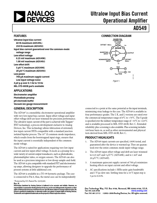
Ultralow Input Bias Current Operational Amplifier AD549
CONNECTION DIAGRAM
GUARD PIN, CONNECTED
TO CASE
OFFSET NULL
8
V+
1 AD549 7
INVERTING INPUT
2
6 OUTPUT
3 NONINVERTING
4. AC specifications include 1 MHz unity-gain bandwidth and 3 V/μs slew rate. Settling time for a 10 V input step is 5 μs to 0.01%.
One Technology Way, P.O. Box 9106, Norwood, MA 02062-9106, U.S.A.
Tel: 781.329.4700
Fax: 781.461.3113 ©2002–2008 Analog Devices, Inc. All rights reserved.
元器件交易网
AD549
TABLE OF CONTENTS
Features .............................................................................................. 1 Applications....................................................................................... 1 Connection Diagram ....................................................................... 1 General Description ......................................................................... 1 Product Highlights ........................................................................... 1 Revision History ............................................................................... 2 Specifications..................................................................................... 3 Absolute Maximum Ratings............................................................ 5
AD590中文资料

AD590中文资料1.引言集成温度传感器将温敏晶体管与相应的辅助电路集成在同一块芯片上,能直接给出正比于绝对温度的理想线性输出,一般用于-55℃~±150℃之间的温度测量。
温敏晶体管在管子的集电极电流恒定时,其基极发射极电压与温度成线性关系,为克服温敏晶体管vb电压产生时的离散性,采用了特殊的差分电路。
集成温度传感器具有电压型和电流型两种,电流输出型集成温度传感器在一定的温度T时相当于一个恒流源。
因此,它不易受接触电阻、引线电阻、电压噪音的干扰,具有很好的线性特性。
本实验采用国产的AD590,它只需要一种电源(4.5~24V)即可实现温度到电流的线性变换,然后在终端使用一只取样电阻,即可实现电流到电压的转换。
它使用方便,并且电流型比电压型的测量精度高。
2.传感器的特性测量2.1实验内容测量AD590在电源电压稳定时,输出电流与温度的关系及不同温度下的伏安特性,采用图1所示电路。
实验中为了测量不同温度下的AD590的特性,必须将AD590用铝外壳保护且引线用绝缘材料封闭,置于恒温水浴中。
伏特表测量电阻两端的电压。
由于AD590近似于高精度电流源,所以要求伏特表有足够的测量精度,本实验采用了三位半数字电压表测量电压值。
对于电阻R,一方面要有足够的有效数字,另一方面其压降又要使伏特表的读数有足够的有效数字。
本实验采用了0.1级电阻箱。
数值为200.0,由I=V/R,即得AD590上的电流值。
以温度作为自变量,电流I为因变量,方程为:2.2数据处理表1为实验测得的一组数据,显示温度和电流的关系(R=200)。
用最小二乘法进行拟合,通过计算机程序,输入10组实验数据计算得出、和相关系数,程序如图2所示。
3. 测温电路3.1实验内容设计一个用AD590精确测量0~100℃范围内温度的电路,为使伏特表的示数正好是摄氏温度的读数,取R1上的电压与R2上的分压差作为V的输入。
测温电路如图3所示。
图3中电阻值根据伏安特性测量时用最小二乘法拟合结果计算得出。
AD数据手册部分内容中文翻译
AD9959数据手册(部分)GENERAL DESCRIPTION概述The AD9959 consists of four direct digital synthesizer (DDS) cores that provide independent frequency, phase, and amplitude control on each channel. This flexibility can be used to correct imbalances between signals due to analog processing, such as filtering, amplification, or PCB layout-related mismatches. Because all channels share a common system clock, they are inherently synchronized. Synchronization of multiple devices is supported. The AD9959 can perform up to a 16-level modulation of frequency, phase, or amplitude (FSK, PSK, ASK). Modulation is performed by applying data to the profile pins. In addition, the AD9959 also supports linear sweep of frequency, phase, or amplitude for applications such as radar and instrumentation.AD9959含有四个直接数字频率合成器(DDS),提供各通道独立的频率、相位和振幅控制。
AD549JHZ资料

1. The AD549 input currents are specified, 100% tested, and guaranteed after the device is warmed up. They are guaranteed over the entire common-mode input voltage range.
Ultralow Input Bias Current Operational Amplifier AD549
CONNECTION DIAGRAM
GUARD PIN, CONNECTED
TO CASE
SET NULL
8
V+
1 AD549 7
INVERTING INPUT
2
6 OUTPUT
3 NONINVERTING
2. The AD549 input offset voltage and drift are laser trimmed to 0.25 mV and 5 μV/°C (AD549K), and to 1 mV and 20 μV/°C (AD549J).
3. A maximum quiescent supply current of 700 μA minimizes heating effects on input current and offset voltage.
ESD Caution.................................................................................. 5 Typical Performance Characteristics ............................................. 6 Functional Description .................................................................. 10
微光信号检测系统
基于AD549的微光信号检测系统引言近年来,随着微光技术及生物芯片技术的高速发展,各类的传感器、光电器件应运而生,广泛应用于工业,农业,军事等各大领域。
然而技术水平的不断提高就要求研究设备对微光信号的响应程度的大幅提高。
微光信号检测是发展高新技术、科学研究的重要手段,微光信号检测精度的高低往往会对产品的性能等起到决定性的作用。
在微光信号检测系统中,通常光电转换器件接收到的光信号都十分的微弱,转换后的电信号也非常的小(nA量级)。
因此,放大器噪声,背景噪声,电路噪声,外界电磁干扰等都会对检测系统的精度产生极大的影响。
为此,选择一个合适的低噪声高精度的前置放大器就显得至关重要了。
本文的微光信号检测系统选用的前置放大器是AD549。
它是具有极低输入偏置电流的单片电路静电计型运算放大器。
为达到高精度的目的,输入偏置电压和输入偏置电压漂移均通过激光调节。
这种极低输入电流性能由ADI公司专有的topgate工艺技术完成。
这样的放大器很好的满足了系统的需要。
1.微光信号检测系统的原理框图微光信号检测系统的原理框图如图1所示。
光信号由光电阴极转换为电信号输入到前置放大器中,经过一级放大的电压信号由二级放大器放大之后再输入到AD转换器件中转换成数字信号,之后经由单片机控制显示出来。
为了防止模拟电路同数字电路间的串扰,及前置放大器屏蔽的需要,本系统将两部分的电路分离开来。
光电检测电路由光电阴极和前置放大器AD549组成,数字显示电路由二级放大器OPA124PA,AD转换器件ADS7816,单片机及数字显示电路组成。
图1 微光信号检测系统的原理框图2.光电检测电路2.1 光电检测电路原理图2 光电检测电路图2为光电检测电路图。
光电阴极是一种灵敏度很高的光电器件,可探测极为微弱的光信号。
光信号经过转换之后输出微弱电信号到前置放大器AD549。
它有极低的偏置电流60fA,输入级具有1015Ω的共模阻抗,其输入电流与共模电压无关。
- 1、下载文档前请自行甄别文档内容的完整性,平台不提供额外的编辑、内容补充、找答案等附加服务。
- 2、"仅部分预览"的文档,不可在线预览部分如存在完整性等问题,可反馈申请退款(可完整预览的文档不适用该条件!)。
- 3、如文档侵犯您的权益,请联系客服反馈,我们会尽快为您处理(人工客服工作时间:9:00-18:30)。
极低偏置电流运算放大器AD5491 概述AD549是具有极低输入偏置电流的单片电路静电计型运算放大器。
为达到高精度的目的,输入偏置电压和输入偏置电压漂移均通过激光调节。
这种极低输入电流性能由ADI公司专有的topgate工艺技术完成。
该技术可以制造与具有极低输入电流的JFET并与双极性电路隔离的集成运放。
输入级具有1015Ω的共模阻抗,其输入电流与共模电压无关。
AD549适用于低输入电流和低输入偏置电压的场合。
它特别适合用作各种电流输出的传感器,如光电二极管、光电倍增管以及氧气传感器等的前置放大器。
该产品也可用作精密积分器或低衰减采样保持器。
AD549的封装与标准FET和静电计运算放大器兼容,因此用户花少量成本即可对系统升级,提高已有系统的性能。
AD549有TO-99密封封装。
金属外壳与8管脚相连,使得金属外壳与同样电压的输入终端独立连接,达到降低外壳泄漏的目的。
AD549具有四种性能等级。
其中J、K和L型号的温度范围是0℃到70℃。
S型号专用于军事,其温度范围:-55℃到125℃。
AD549的输入电流在整个共模输入电压范围内都得到保证,其输入失调电压和漂移由激光分别调节到和5μV/℃(AD549K);1mV和20μV/℃(AD549J)。
700μA的最大静态电流使输入电流和偏置电压的热效应降到最低。
模拟性能包括1MHz的均匀增益带宽和3V/μs的压摆率。
当输入为10V时,建立时间是5μs 到%。
2 AD549的引脚及特性参数图一所示是AD549的引脚图,表一所示是其特性参数。
参数AD549J最小典型最大AD549K最小典型最大AD549L最小典型最大AD549S最小典型最大单位输入偏置电流共模输入,V CM=0V共模输入,V CM=±10V 共模输入T MAX,V CM=0V 失调电流T MAX处失调电流15025015025011507510075100304060406020751007510042030125fAfApAfApA输入失调电压失调T MAX处失调电压受温度的影响受电源的影响T MIN~T MAX,受电源影响长时间失调稳定性0.510203210032100152 510 3210 32150.35 1010 3210 32150.310151032325015mVmVμV/℃μV/VμV/VμV/month输入电压噪声f= ~10Hz f=10Hz f=100Hz f=1kHz4906035354690603535490603535490603535μVp-pnV/nV/nV/nV/图一AD549引脚图表一AD549的主要特性f=10kHz输入电流噪声f= ~10Hz f=10kHz fA rms fA/输入阻抗差模V DFF =±1共模V CM =±101013‖11015‖1013‖11015‖1013‖11015‖1013‖11015‖Ω‖pFΩ‖pF开环增益V0@±10V,R L=10kΩV0@±10V,R L=10kΩ, T MIN/T MAXV0=±10V,R L=10kΩV0=±10V,R L=10kΩ, T MIN/T MAX 300 1000300 800100 25080 200300 1000300 800100 25080 200300 1000300 800100 25080 200300 1000300 800100 25025 150V/mVV/mVV/mVV/mV输入电压范围差模电压共模电压共模抑制比V=+10V,-10V T MIN/T MAX±20-10 +10809076 80±20-10 +109010080 90±20-10 +1090 10080 90±20-10 +1090 10080 90VVdBdB输出性能电压@R L=10kΩ,T MIN/T MAX 电压@R L=2kΩ,T MIN/T MAX 短路电流T MIN/T MAX负载电容稳定性G=+1-12 +12-10 +1015 20359-12 +12-10 +1015 20359-12 12-10 +1015 20359-12 +12-10 +1015 20 3564000VVmAmApF3 AD549的工作原理最小化输入电流AD549具有很小的输入电流和失调电压。
在实际应用中应谨慎考虑如何使用放大器可以减小输入电流。
为减小输入电流,该放大器的工作温度应尽可能低。
像其他JFET 输入放大器一样,AD549的输入电流对芯片温度很敏感,上升斜率因子为每10℃的。
图二所示为AS549不同环境温度时的输入电流。
40004000 4000 频率响应单位增益,小信号全功率响应压摆率建立时间,%建立时间,%过载恢复,50%,G=-1502 35250 2 35 2 50 2 35 2 50 2 35 2MHz kHz V/μs μs μs μs 电源供给 额定性能工作静态电流 ±15 ±5 ±18±15 ±5 ±18 ±15 ±5 ±18 0 .70 ±15 ±5 ±18 V V mA 温度范围工作,额定性能存储+70-65 +150+70-65 +150 0+70-65 +150-55 +70 -65 +150 ℃ ℃封装选择 TO-99(H-08A)芯片AD549JH AD549KHAD549LHAD549SH/883B图二环境温度对输入偏置电流的影响芯片电源损耗使工作温度上升,从而导致输入偏置电流上升。
由于AD549具有极低的静态供应电流,当放大器工作在15V时,芯片温度不会比环境温度高出3℃。
这种情况下输入电流的差异可以忽略。
但大输出负载可引起芯片温度和输入电流的显著增加,因此建议最小负载阻抗不小于10Ω。
电路板设计注意事项很多原因会产生伪电流,从而降低电流测量的精度。
在放大器信号和电源线之间应有大于1015Ω的绝缘阻抗,以获得低输入电流。
然而标准的PCB材料不具备如此高的绝缘阻抗,因此输入线应与具有足够大电阻系数的绝缘材料相连。
为保持其电阻系数,绝缘体的表面应保持干净。
选择绝缘材料时,除了大容量和高表面电阻系数,还要考虑其他性能。
由于表面水膜层会大大减小绝缘性,防止吸水也很重要。
同样需要考虑的因素还有压电效应(机械压力产生电子激发)和静电效应(摩擦产生电子)。
由于这些机理产生的电子不平衡将表现为寄生泄漏电流。
用通过输入电压偏压的金属导体包围输入线有两个好处:一是由于金属导体和输入线之间的电压很小,因此信号线的寄生漏电减小。
二是输入点的分布电容减小。
输入电容可显著地降低信号带宽和电流/电压转换器的稳定性。
使8管脚封装处于AD549输入电压附近,从而减小封装泄漏和输入共模电容。
图三、图四为反向放大器和同相放大器的保护电路图。
其他保护措施还包括:使电线布局紧凑,减小输入线的长度。
所有精密的高阻抗电路都需要屏蔽干扰噪声。
使用低噪声共轴和三轴电缆以尽量隔离输入信号线。
失调电压的补偿AD549的输入失调电压可通过平衡管脚1和5来调整,见图五。
用这种方式补偿输入失调电压将引入一个附加的输入失调电压漂移,大小为每毫伏μV/℃。
AD549K、AD549L和AD549J的最大附加漂移分别是μV/℃、μV/℃和μV/℃。
图六所示方法可用于放大器用作反向器的场合。
这种方法在放大器负输入终端和电源间引入一个参考电压。
放大器的输入失调电压漂移不受影响。
但电源电压的波动将引起失调电压漂移。
高内阻信号源和高反馈阻抗的交流响应电源和反馈阻抗大于100kΩ时,输入电容的影响放大了电路的交流特性。
由于电路带宽和稳定性互相影响,应考虑共模和差分输入电容产生的影响。
在随后级,电源阻抗和单极输入共模电容把带宽限制在½πR S C S。
把器件的金属外壳和管脚8与输出相连可减小电容的影响。
AD549共模输入电容的典型值是。
在反相放大器的结构中,差分输入电容形成环路传递函数的一极,并导致响应的过冲和不稳定。
可用一个反馈电容稳定电路。
AD549差模输入电容的典型值是1pF。
共模输入电压过载额定共模输入电压范围是小于正电源电压3V到大于负电源电压5V。
超过这个范围将降低放大器的共模抑制比。
共模电压高于正电源电压将导致放大器输出级饱和。
当输入恢复到图三反向放大器的保护电路图图四同向放大器的保护电路图图五标准失调电压补偿电路图六用作反向器时的失调电压补偿电路正常值范围内后,典型的恢复时间为2μs。
输入共模电压在负电源电压1V内将导致输出信号相位翻转。
这种情况下,在输入电压回到正常值范围后μs内运放恢复正常工作。
差模输入电压过载图七所示为不同差模输入电压下AD549的的输入电流。
差模电压在1V到内时,两端输入电流在几百fA内。
超出此范围,输入电流在30μA内。
输入保护AD549可以轻易处理供给电压范围内的任何输入电压。
在没有保护的情况下,输入端电压超过电源供给电压会损坏器件,造成输入电流漂移或偏置电压漂移。
图八所示是放大器用作反相器时的保护电路图。
R P将瞬时过电压产生的电流限制在1mA以内(持续时间小于1秒),或连续电流小于100μA。
由于R P处在反馈电路中,并且远小于放大器输入阻抗值,因此不会影响反相器的直流增益。
但电阻器的热噪声增加了放大器的输入噪声。
在AD549用作跟随器的保护电路中(图九),正输入端的和电容引入½πRC的极点。
同样,R P的热噪声增大了放大器的输入电压噪声。
如图十所示为AD549用作反相器并具有输入钳位电压的电路图。
钳位二极管与反相输入端相连,减小超过钳位的电压值。
由于二极管电流低,还可减小漏电流。
应使用低渗漏二极管如FD333并防止照射以防止光电流产生。
即使采取这些措施,二极管的输入电流和电容仍会有所增加。
图七不同差模输入电压下的输入电流图八有输入电流限制的反相放大器图九有输入电流限制的跟随器图十具有输入钳位的反相放大器4 应用电路漏电流的采样和测量有很多方法,如电流积分和直接将电流转换为电压,可测量微弱的漏电流。
无论哪种方法,为准确测量都应考虑电路板和连线的整洁、绝缘材料的选择、保护技术和布线排版。
图十一是采样和差动电路。
电路包括两个AD549静电计放大器用作电流电压转换器,和高阻值(1010Ω)的传感电阻(RSa和RSb)。
R1和R2提高了电路的总灵敏度,其值为10fA/mV (满量程10pA)。
C C和C F用作抑制噪声和闭环补偿。
C C应是一个低渗漏的聚苯乙烯电容。
测量时使用极低渗漏的Kel-F测试插座连接器件。