MSP430g2553原理图
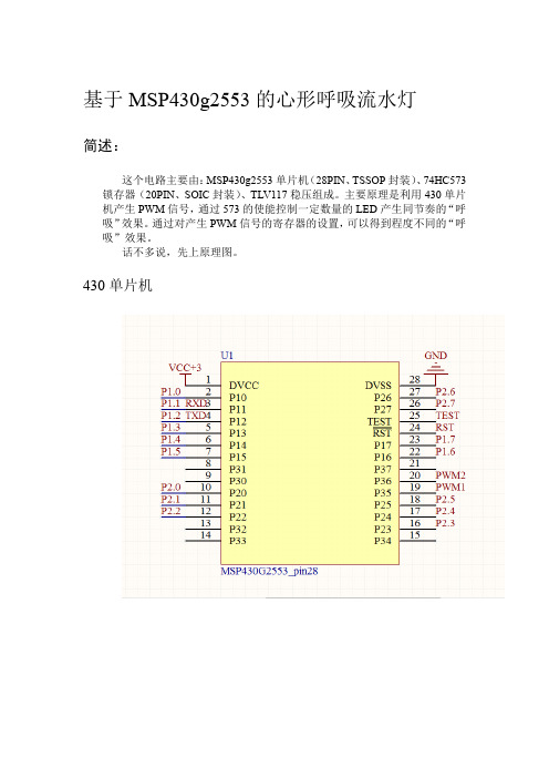
基于MSP430g2553的心形呼吸流水灯
430注意!在画原理图的时候,需留出一个跳线接口,在编程调 试的时候要将复位电路与 430 电路的连接断开( C3 电容会 对编程调试时的数据传输产生影响) 。另一个解决办法是: 去掉 C3 电容,在复位电路与 430 电路之间加一个 2K 的电 阻。
如图所示
锁存器和 LED
breath_down(500,0x01,0xFF); breath_up(500,0xFF,0xFF); delayms(500); breath_down(500,0xFF,0xFF); P1OUT=0x00; P2OUT=0x00; delayms(500); flicker(0x8E,0xE3,6,100); 闪烁“笑脸” for(i=4;i>0;i--) //呼吸 { breath_up(1000,0xFF,0xFF); delayms(500); breath_down(1000,0xFF,0xFF); } P2OUT=0x80; P1OUT=0x00; delayms(500); P2OUT=0x40; P1OUT=0x00; delayms(500); while(1) //两个 LED“永无止境的追逐” { run_two(1); } } }
Made by Wonder 由于能力有限,如有错误,请多多包涵! 如有更好的方案,wondertmac@,欢迎来件交流。
基于 MSP430g2553 的心形呼吸流水灯
简述:
这个电路主要由: MSP430g2553 单片机 (28PIN、 TSSOP 封装) 、 74HC573 锁存器(20PIN、SOIC 封装) 、TLV117 稳压组成。主要原理是利用 430 单片 机产生 PWM 信号, 通过 573 的使能控制一定数量的 LED 产生同节奏的 “呼 吸” 效果。 通过对产生 PWM 信号的寄存器的设置, 可以得到程度不同的 “呼 吸”效果。 话不多说,先上原理图。
MSP430g2553课件

(演示)
南京航空航天大学电子中心&TI南航430联合实验室
如何改变发光二级管闪烁的速度?
改变延时的时间参数
1、亮 2、延时1秒钟 3、熄灭 4、延时1秒钟 5、跳转到 步骤1
(演示)
南京航空航天大学电子中心&TI南航430联合实验室
如何让一只发光管闪快、另一只慢?
增加一个变量xx
南京航空航天大学电子中心&TI南航430联合实验室
MSP430单片机学习方法
强化理论知识 大量做实验 勤于思考 多动手
已经与MSP430厂家———TI(德州仪器) 建立了联合实验室,拥有60套实验设备。 地点:3410。其中40套为赠送,20套购买
南京航空航天大学电子中心&TI南航430联合实验室
while(条件表达式) 语句; 当条件满足时,就反复执行后面的语 句,一直执行到条件不满足时。以软件 延时程序为例说明该语句是如何执行的。 void delay(long v) { while(v!=0)v--; }
南京航空航天大学电子中心&TI南航430联合实验室
P1
P2
P3 P4
P5 P6
南京航空航天大学电子中心&TI南航430联合实验室
引脚控制寄存器
PnDIR PnOUT PnIN PnSEL
方向寄存器 1为输出、0为输入 输出寄存器 1输出高、0为低 输入寄存器 读出口线的状态 第二功能寄存器 n=1,2,3,4,5,6
南京航空航天大学电子中心&TI南航430联合实验室
南京航空航天大学电子中心&TI南航430联合实验室
MSP430g2553原理图
MSP-EXP430G2LaunchPad Evaluation Kit User's GuideLiterature Number:SLAU318EJuly2010–Revised March2014Contents 1MSP-EXP430G2LaunchPad Overview (4)1.1Overview (4)1.2Features (5)1.3Kit Contents (5)1.4Revisions (6)2Installation (6)2.1Download the Required Software (6)2.2Install the Software (6)2.3Install the Hardware (6)3Getting Started With MSP-EXP430G2LaunchPad (7)3.1Getting Started (7)3.2Demo Application,Internal Temperature Measurement (7)4Develop an Application With the MSP-EXP430G2LaunchPad (8)4.1Developing an Application (8)4.2Program and Debug the Temperature Measurement Demo Application (8)4.3Disconnect Emulator From Target With Jumper J3 (9)4.4Program Connected eZ430Target Boards (10)4.5Connecting a Crystal Oscillator (10)4.6Connecting a BoosterPack (11)4.7Supported Devices (11)4.8MSP-EXP430G2On-Board Emulator (13)5MSP-EXP430G2Hardware (13)5.1Device Pinout (13)5.2Schematics (14)5.3PCB Layout (20)5.4Bill of Materials(BOM) (23)6Suggested Reading (24)7Frequently Asked Questions(FAQ) (24)Revision History (26)2Table of Contents SLAU318E–July2010–Revised March2014Submit Documentation FeedbackCopyright©2010–2014,Texas Instruments IncorporatedList of Figures1MSP-EXP430G2LaunchPad Overview (5)2Insert Device Into Target Socket (8)3Code Composer Studio™v4in Debugging Mode (9)4MSP-EXP430G2LaunchPad With Attached eZ430-RF2500Target Board (10)5Device Pinout (13)6Schematics,MSP-EXP430G2Emulator(1of2),Revision1.4 (14)7Schematics,MSP-EXP430G2Emulator(2of2),Revision1.4 (15)8Schematics,MSP-EXP430G2Target Socket,Revision1.4 (16)9Schematics,MSP-EXP430G2Emulator(1of2),Revision1.5 (17)10Schematics,MSP-EXP430G2Emulator(2of2),Revision1.5 (18)11Schematics,MSP-EXP430G2Target Socket,Revision1.5 (19)12Layout,LaunchPad Top Layer (20)13Layout,LaunchPad Bottom Layer (21)14Layout,LaunchPad Silkscreen (22)List of Tables1Jumper Connection J3Between Emulator and Target (9)2eZ430Debugging Interface (10)3Supported Devices (11)4Features Supported by On-Board Emulator (13)5Bill of Materials (23)3 SLAU318E–July2010–Revised March2014List of Figures Submit Documentation FeedbackCopyright©2010–2014,Texas Instruments IncorporatedUser's GuideSLAU318E–July2010–Revised March2014 MSP-EXP430G2LaunchPad Evaluation KitPreface:Read This FirstIf You Need AssistanceIf you have any feedback or questions,support for the MSP430™devices and the MSP-EXP430G2isprovided by the Texas Instruments Product Information Center(PIC)and the TI E2E Forum(/).Contact information for the PIC can be found on the TI web site at .Additional device-specific information can be found on the MSP430web site at /msp430. Related Documentation from Texas InstrumentsThe primary sources of MSP430information are the device-specific data sheets and user's guidesavailable at the Texas Instruments MSP430web site:/msp430.MSP430device user's guides,application reports,software examples and other MSP430user's guides can be found at the Tech Docs section.The CCS user's guide includes detailed information on setting upa project and using Code Composer Studio™for the MSP430microcontroller(SLAU157).Information specific to the MSP-EXP430G2LaunchPad Evaluation Kit,all the available IDEs,Software Libraries,and examples can be found at the Tools&Software section:/tool/msp-exp430g2.1MSP-EXP430G2LaunchPad Overview1.1OverviewThe MSP-EXP430G2LaunchPad is an inexpensive and simple evaluation kit for the MSP430G2xx Value Line series of microcontrollers.It is an easy way to start developing on the MSP430with on-boardemulation for programming and debugging as well as buttons and LEDs for a simple user interface.Rapid prototyping is simplified by the20-pin BoosterPack headers which support a wide range of available BoosterPack plug-in modules.You can quickly add features like wireless connectivity,graphical displays, environmental sensing,and much more.You can either design your own BoosterPack or choose among many already available from TI and third party developers.The LaunchPad features an integrated DIP target socket that supports up to20pins,allowing MSP430™Value Line devices to be plugged into the LaunchPad board.The MSP-EXP430G2LaunchPad comeswith an MSP430G2553device by default.The MSP430G2553has the most memory available of thecompatible Value Line devices.The MSP430G255316-bit MCU has16KB flash,512bytes RAM,up to16-MHz CPU speed,10-bit ADC, capacitive touch enabled I/Os,universal serial communication interface,and more–plenty to get youstarted in your development.Free software development tools are also available:TI's Eclipse-based Code Composer Studio™IDE(CCS),IAR Embedded Workbench™IDE(IAR),and the community-driven Energia open source codeeditor.More information about the LaunchPad,including documentation and design files,can be found on the tool page at /tool/msp-exp430g2.MSP430,Code Composer Studio are trademarks of Texas Instruments.IAR Embedded Workbench is a trademark of IAR Systems.All other trademarks are the property of their respective owners.4MSP-EXP430G2LaunchPad Evaluation Kit SLAU318E–July2010–Revised March2014Submit Documentation FeedbackCopyright©2010–2014,Texas Instruments Incorporated MSP-EXP430G2LaunchPad Overview 1.2FeaturesMSP-EXP430G2LaunchPad features:•USB debugging and programming interface featuring a driverless installation and application UART serial communication with up to9600Baud•Supports MSP430G2xx2,MSP430G2xx3,and MSP430F20xx devices in PDIP14or PDIP20packages (see Section4.7for a complete list of supported devices)•Two general-purpose digital I/O pins connected to green and red LEDs for visual feedback•Two push button for user feedback and device reset•Easily accessible device pins for debugging purposes or as socket for adding customized extension boards•High-quality20-pin DIP socket for an easy plug-in or removal of the target deviceFigure1.MSP-EXP430G2LaunchPad Overview1.3Kit ContentsThe MSP-EXP430G2evaluation kit includes the following hardware:•LaunchPad emulator socket board(MSP-EXP430G2)•Mini USB-B cable,0.5m•Two MSP430flash devices–MSP430G2553:Low-power16-bit MSP430microcontroller with an8-channel10-bit ADC,on-chip comparator,touch-sense enabled I/Os,universal serial communication interface,16kB flashmemory,and512bytes of RAM(preloaded with a sample program)–MSP430G2452:Low-power16-bit MSP430microcontroller with an8-channel10-bit ADC,on-chip comparator,touch-sense enabled I/Os,universal serial interface,8kB flash memory,and256bytesof SRAM•Two10-pin PCB connectors female•32.768-kHz clock crystal from Micro Crystal()•Quick start guide•Two LaunchPad stickers5 SLAU318E–July2010–Revised March2014MSP-EXP430G2LaunchPad Evaluation Kit Submit Documentation FeedbackCopyright©2010–2014,Texas Instruments IncorporatedInstallation 1.4RevisionsThe first production revision of the LaunchPad in2010was1.3.In2012the LaunchPad board revision changed from1.4to1.5to align with the new release of Value Line devices.The differences in theschematic and the kit contents are:•Layout and Schematic:–Voltage feedback in the emulator changed to increase startup stability(Rev1.3to Rev1.4)–Rearranged jumper J3to support two UART configurations:vertical(SW UART),horizontal(HW UART)–VCC on the connector J4can now be disconnected from the emulator VCC by J3–Pullup resistor R34and capacitor C24on P1.3removed to reduce the current consumption–Presoldered male headers J1and J22InstallationThe MSP-EXP430G2LaunchPad installation consists of three easy steps:1.Download the required software.2.Install the selected IDE.3.Connect the LaunchPad to the PC.Then the LaunchPad is ready to develop applications or to use the pre-programmed demo application.2.1Download the Required SoftwareDifferent development software tools are available for the MSP-EXP430G2LaunchPad developmentboard.IAR Embedded Workbench™KickStart IDE and Code Composer Studio™(CCS)IDE are bothavailable in a free limited version.IAR Embedded Workbench allows4KB of C-code S is limited to a code size of16KB.The software is available at /mspds.There are manyother compilers and integrated development environments(IDEs)available to use with the MSP-EXP430 LaunchPad including Rowley Crossworks and MSPGCC.However,example projects have been created using IAR Embedded Workbench KickStart IDE and Code Composer Studio IDE(CCS).For moreinformation on the supported software and the latest code examples,visit the LaunchPad tool page(/tool/msp-exp430g2).2.2Install the SoftwareDownload one of the integrated development environments(IDEs)(see Section2.1).IAR KickStart and CCS offer the required driver support to work with the MSP-EXP430LaunchPad onboard emulation.Once installed,the IDE should find the MSP-EXP430G2LaunchPad as USB:HID debugging interface.Now all is set for developing MSP430G2xx based application on the LaunchPad.2.3Install the HardwareConnect the MSP-EXP430G2LaunchPad socket board with the enclosed USB cable to a PC.The driver installation starts automatically.If prompted for software,allow Windows to install the softwareautomatically.This is possible only if either IAR KickStart or CCS is already installed.6MSP-EXP430G2LaunchPad Evaluation Kit SLAU318E–July2010–Revised March2014Submit Documentation FeedbackCopyright©2010–2014,Texas Instruments Incorporated Getting Started With MSP-EXP430G2LaunchPad 3Getting Started With MSP-EXP430G2LaunchPad3.1Getting StartedThe first time the MSP-EXP430G2LaunchPad Evaluation Kit is used,a demo application automatically starts as soon as the board is powered from the USB host.To start the demo,connect the MSP-EXP430G2LaunchPad with the included mini USB cable to a free USB port.The demo application starts with an LED toggle to show the device is active.More information about the demo application can befound in Section3.2.3.2Demo Application,Internal Temperature MeasurementThe LaunchPad includes a pre-programmed MSP430G2553device already installed in the target socket.When LaunchPad is connected via USB,the demo starts with an LED toggle sequence.The onboardemulation generates the supply voltage and all the signals necessary to start.Press button P1.3to switch the application to a temperature measurement mode.A reference temperature is taken at the beginning of this mode,and the LEDs of the LaunchPad signal a rise or fall in temperature by varying the brightness of the on-board red or green LED,respectively.The reference temperature can also be recalibrated with another button press on P1.3.The collected temperature data is alsocommunicated via back-channel UART through the USB emulation circuitry back to the PC.The internal temperature sensor data from the MSP430G2553device is sent to the PC to be displayed on the GUI.The pre-loaded demo application and the GUI are found in the Software Examples zip folder.The GUI is opened with LaunchPad_Temp_GUI.exe.This GUI is made with Processing()with the source available for customization.The serial communication port on the PC must be configured with 2400bps,one stop bit,and no flow control to display the values correctly.The demo application uses the on-chip peripherals of the MSP430G2553device such as the10-bit ADC, which samples the internal temperature sensor,and16-bit timers,which drive the PWM to vary brightness of the LEDs and enable software UART for communication with the PC.The MSP430G2553offers a USCI interface that is capable of communicating through UART at up to2MBaud,but to be aligned with all the other MSP430G2xx devices,the demo uses the Timer UART implementation,which can be used on all the other devices.This way the demo can be used with any other MSP430G2xx device with an integrated ADC,without any change in the program.The provided applications can be a great starting point for various custom applications and give a good overview of the various applications of the MSP430G2xx Value Line devices.7 SLAU318E–July2010–Revised March2014MSP-EXP430G2LaunchPad Evaluation Kit Submit Documentation FeedbackCopyright©2010–2014,Texas Instruments Incorporated4Develop an Application With the MSP-EXP430G2LaunchPad4.1Developing an ApplicationThe integrated development environments(IDEs)shown in Section2offer support for the wholeMSP430G2xx Value Line.The MSP-EXP430G2LaunchPad needs only a connection to the USB of the Host PC—there is no external hardware required.The power supply and the Spy-Bi-Wire JTAG signals TEST and RST must be connected with jumper J3to allow the onboard emulation connection to thedevice.Now the preferred device can be plugged into the DIP target socket of the LaunchPad(seeFigure2).Both PDIP14and PDIP20devices of the MSP430G2xx Value Line and the MSP430F20xxfamily can be inserted into the DIP socket aligned to pin1.A complete list of supported devices can be found in Section4.7.Figure2.Insert Device Into Target SocketThe following example for Code Composer Studio shows how to download and debug the demoapplication described in Section3.2.4.2Program and Debug the Temperature Measurement Demo ApplicationThe source code of the demo application can be found in the Software Examples zip folder.Download the project folder and unpack it to a location of your choice.For this demo,Code Composer Studio v4ornewer must be installed.The demo application can be loaded to the CCS workspace by clicking File→Import.Select the location of the extracted project files and import Existing projects into Workspace.Now the MSP-EXP430G2-Launchpad project appears inside the CCS workspace.The project must be marked as the active project to start programming and debugging the device.Connect the LaunchPad with an inserted MSP430G2553device to the host PC and click the Debug button on the CCS Toolbar.The MSP-EXP430G2LaunchPad is initialized and the download of the compileddemo application starts.The CCS view switches to a debugging interface once the download is completed and the application is ready to start.Figure3shows Code Composer Studio v4with the MSP-EXP430G2 LaunchPad demo application in debug view.8MSP-EXP430G2LaunchPad Evaluation Kit SLAU318E–July2010–Revised March2014Submit Documentation FeedbackCopyright©2010–2014,Texas Instruments IncorporatedFigure3.Code Composer Studio™v4in Debugging Mode4.3Disconnect Emulator From Target With Jumper J3The connection between the MSP-EXP430G2emulator and the attached target device can be opened with the jumper array J3.This can be useful to access an attached eZ430target board by disconnecting the Spi-Bi-Wire JTAG lines RST and TEST or if the JTAG lines are used for other application purposes.The jumper array can also be used to measure the power consumption of the LaunchPad application.For this intention,all connections except VCC must be opened,and a multi meter can used on the VCCJumper to measure the current of the MSP-EXP430G2target device and its peripherals.The jumper J5 VCC also must be opened if the LaunchPad board is powered with an external power supply over J6Table1or the eZ430interface J4.NOTE:The assignment of jumper J3has been changed in MSP-EXP430G2revision1.5,see thecomments in Table1to find the assignment for a specific board revision.Table1.Jumper Connection J3Between Emulator and TargetJumper Signal Description1VCC Target socket power supply voltage(power consumption test jumper)(located on5before Rev.1.5)Test mode for JTAG pins or Spy-Bi-Wire test clock input during programming and test(located on1before 2TESTRev.1.5)3RST Reset or Spy-Bi-Wire test data input/output during programming and test(located on2before Rev.1.5)4RXD UART receive data input(direction can be selected by jumper orientation)(located on3before Rev.1.5)5TXD UART transmit data output(direction can be selected by jumper orientation)(located on4before Rev.1.5)Jumpers4and5connect the UART interface of the emulator to the target device pins P1.1and P1.2.The direction of the UART signal lines can be selected by the orientation of the attached jumpers.In horizontal orientation,the jumpers connect TXD to P1.1and RXD to P1.2,as they are used for the software UART communication on the demo application(see Section3.2).In vertical orientation,the jumpers connect the TXD signal to P1.2and the RXD signal to P1.1,as required for the MSP430G2553USCI.9 SLAU318E–July2010–Revised March2014MSP-EXP430G2LaunchPad Evaluation Kit Submit Documentation FeedbackCopyright©2010–2014,Texas Instruments Incorporated4.4Program Connected eZ430Target BoardsThe MSP-EXP430G2LaunchPad can program the eZ430-RF2500T target boards,the eZ430-Chronos watch module,or the eZ430-F2012T/F2013T.To connect one of the ez430targets,connector J4must be populated with a0.050-in(1.27-mm)pitch male header,as shown in Figure4.Figure4.MSP-EXP430G2LaunchPad With Attached eZ430-RF2500Target Board To program the attached target without interfering with the LaunchPad socket board,jumper connections TEST and RST of J3must be open.The interface to the eZ430target board is always connected to the MSP-EXP430G2emulator,so the programming and debugging of a connected LaunchPad target device is possible only if the eZ430target is not connected on the same time.The application UART,on the other hand,is connected directly to the LaunchPad target device,and jumper J3can be closed to monitor the transmission from the LaunchPad target to the attached eZ430.This way both possible connections,from the device to the PC and from the device to the eZ430,can be established without changing the direction of the UART pins.The VCC connection to the eZ430interface is directly connected to the LaunchPad target VCC and can be separated with jumper J3,if the LaunchPad itself should be powered via a connected battery on J4.To supply the eZ430interface with the onboard emulator the jumper J3VCC needs to be closed.Table2shows the pinout of the eZ430debugging interface J4,the first pin is the left pin located on the emulator part of the LaunchPad.Table2.eZ430Debugging InterfacePin Signal Description1TXD UART transmit data output(UART communication from PC or MSP430G2xx to eZ430target board)2VCC Power supply voltage(J3VCC needs to be closed to supply via onboard emulator)3TEST/SBWTCK Test mode for JTAG pins and Spy-Bi-Wire test clock input during programming and test4RST/SBWTDIO Reset,Spy-Bi-Wire test data input/output during programming and test5GND Power supply ground6RXD UART receive data input(UART communication from eZ430target board to PC or MSP430G2xx)4.5Connecting a Crystal OscillatorThe MSP-EXP430G2LaunchPad offers a footprint for a variety of crystal oscillators.The XIN and XOUT signals of the LFXT1oscillator can support low-frequency oscillators like a watch crystals of32768Hz or a standard crystal with a range defined in the associated data sheet.The signal lines XIN and XOUT can also be used as multipurpose I/Os or as a digital frequency input.More information on the possibilities of the low-frequency oscillator and the possible crystal selection can be found in the MSP430x2xx Family User's Guide(SLAU144)or the device-specific data sheet.The oscillator signals are connected to J2to use the signals on an attached application board.In case of signal distortion of the oscillator signals that leads to a fault indication at the basic clock module,resistors R29and R28can be used to disconnect the pin header J2from the oscillating lines.10MSP-EXP430G2LaunchPad Evaluation Kit SLAU318E–July2010–Revised March2014Submit Documentation FeedbackCopyright©2010–2014,Texas Instruments Incorporated4.6Connecting a BoosterPackThe LaunchPad can connect to many BoosterPacks within the ecosystem.The BoosterPack headers J1 and J2along with power supply J6fall on a100-mil(0.1-in)grid to allow for easy and inexpensivedevelopment with a breadboard.The LaunchPad adheres to the20-pin LaunchPad pinout standard.Astandard was created to aid compatibility between LaunchPads and BoosterPacks,across the TIecosystem.The20-pin standard is backward compatible with the40-pin standard used by LaunchPads like the MSP-EXP430F5529LP.This allows a subset of some40-pin BoosterPacks to be used with20-pin LaunchPads.While most BoosterPacks are compliant with the standard,some are not.The LaunchPad is compatible with all20-pin(and40-pin)BoosterPacks that are compliant with the standard.If the reseller or owner of the BoosterPack does not explicitly indicate compatibility with the MSP430G2LaunchPad,you might want to compare the schematic of the candidate BoosterPack with the LaunchPad,to ensure compatibility.Keep in mind that sometimes conflicts can be resolved by changing the G2device pin functionconfiguration in software.More information about compatibility can also be found at/launchpad.4.7Supported DevicesTexas Instruments offers several MSP430devices in a PDIP package that is compatible with LaunchPad.Table3shows the supported devices.Table3.Supported Devices11 SLAU318E–July2010–Revised March2014MSP-EXP430G2LaunchPad Evaluation Kit Submit Documentation FeedbackCopyright©2010–2014,Texas Instruments IncorporatedTable3.Supported Devices(continued)12MSP-EXP430G2LaunchPad Evaluation Kit SLAU318E–July2010–Revised March2014Submit Documentation FeedbackCopyright©2010–2014,Texas Instruments Incorporated MSP-EXP430G2Hardware 4.8MSP-EXP430G2On-Board EmulatorThe MSP-EXP430G2on-board emulator enables programming and debugging of supported MSP430devices(see Section4.7).It offers several features that are enabled by a2-wire JTAG interface calledSpy-Bi-Wire.For a more feature-complete emulator,the MSP-FET430UIF flash emulation tool may bemore appropriate.See Table4for more details on the MSP-EXP430G2LaunchPad on-board emulator.Table4.Features Supported by On-Board EmulatorSupport by LaunchPadFeature(MSP-EXP430G2) Supports MSP430F20xx,F21x2,F22xx,G2x01,G2x11,G2x21,G2x31,G2x53✓Allows fuse blowAdjustable target supply voltageFixed2.8-V target supply voltageFixed3.6-V target supply voltage✓4-wire JTAG2-wire JTAG✓Application UART✓Supported by CCS✓Supported by IAR✓5MSP-EXP430G2Hardware5.1Device PinoutFigure5.Device Pinout13 SLAU318E–July2010–Revised March2014MSP-EXP430G2LaunchPad Evaluation Kit Submit Documentation FeedbackCopyright©2010–2014,Texas Instruments IncorporatedMSP-EXP430G2Hardware 5.2SchematicsFigure6.Schematics,MSP-EXP430G2Emulator(1of2),Revision1.414MSP-EXP430G2LaunchPad Evaluation Kit SLAU318E–July2010–Revised March2014Submit Documentation FeedbackCopyright©2010–2014,Texas Instruments Incorporated MSP-EXP430G2HardwareFigure7.Schematics,MSP-EXP430G2Emulator(2of2),Revision1.415 SLAU318E–July2010–Revised March2014MSP-EXP430G2LaunchPad Evaluation Kit Submit Documentation FeedbackCopyright©2010–2014,Texas Instruments IncorporatedMSP-EXP430G2Hardware Figure8.Schematics,MSP-EXP430G2Target Socket,Revision1.416MSP-EXP430G2LaunchPad Evaluation Kit SLAU318E–July2010–Revised March2014Submit Documentation FeedbackCopyright©2010–2014,Texas Instruments Incorporated MSP-EXP430G2HardwareFigure9.Schematics,MSP-EXP430G2Emulator(1of2),Revision1.517 SLAU318E–July2010–Revised March2014MSP-EXP430G2LaunchPad Evaluation Kit Submit Documentation FeedbackCopyright©2010–2014,Texas Instruments IncorporatedMSP-EXP430G2Hardware Figure10.Schematics,MSP-EXP430G2Emulator(2of2),Revision1.518MSP-EXP430G2LaunchPad Evaluation Kit SLAU318E–July2010–Revised March2014Submit Documentation FeedbackCopyright©2010–2014,Texas Instruments Incorporated MSP-EXP430G2HardwareFigure11.Schematics,MSP-EXP430G2Target Socket,Revision1.519 SLAU318E–July2010–Revised March2014MSP-EXP430G2LaunchPad Evaluation Kit Submit Documentation FeedbackCopyright©2010–2014,Texas Instruments IncorporatedMSP-EXP430G2Hardware 5.3PCB Layoutyout,LaunchPad Top Layer20MSP-EXP430G2LaunchPad Evaluation Kit SLAU318E–July2010–Revised March2014Submit Documentation FeedbackCopyright©2010–2014,Texas Instruments Incorporated MSP-EXP430G2Hardwareyout,LaunchPad Bottom Layer21 SLAU318E–July2010–Revised March2014MSP-EXP430G2LaunchPad Evaluation Kit Submit Documentation FeedbackCopyright©2010–2014,Texas Instruments IncorporatedMSP-EXP430G2Hardware yout,LaunchPad Silkscreen22MSP-EXP430G2LaunchPad Evaluation Kit SLAU318E–July2010–Revised March2014Submit Documentation FeedbackCopyright©2010–2014,Texas Instruments Incorporated MSP-EXP430G2Hardware 5.4Bill of Materials(BOM)Table5.Bill of MaterialsNumberPos.Ref Name Descriptionper Board1C2,C3216pF0402(33pF on Rev1.3)2C9,C10222pF04023C1110nF04024C5,C7,C11,C12,C135100nF04025C4,C6,C831µF,6.3V06046D111N4148MicroMELF7EZ_USB1Mini-USB connector8Q11SMD oscillator12MHz9R1,R2,R3,R16,R17347k0402(R16,R17is not populated)10R8161k50402(6k8in Rev1.3and prior)11R19,R2223k3040212R9130k0402(3k3in Rev1.3and prior)13R12,R21233k040214R4,R5,R6,R7,R235100R040215R14,R15233R040216R18,R202100k040217R13,R24,R2531k5040218R10110k040219R11115k040220U11MSP430F1612IPMR21U41TPD2E001DRLR22U31TUSB3410VF23U21TPS77301DGKR24U51I2C EEPROM128k(AT24C128-10TU-2.7)TP1,TP2,TP3,TP4,25TP5,TP6,TP726C1411nF,SMD060327C21,C2212.5pF,SMD0603(not populated)28C23110µF,10V,SMD080529C20,C241100nF,SMD0603(C24is not populated)30LED0,LED12Green DIODE060331LED21Red DIODE060332R34,R27147k SMD0603(R34is not populated)33R32,R262270R SMD060334R331470R SMD060335R28,R2920R SMD060336IC11DIP20socketClock crystal32kHz(Micro Crystal MS3V-T1R32.768kHz CL:12.5pF±20ppm 37Q2included)38J1,J2,210-pin header,TH,2.54mm male(female header included)39J312X05pin header male40J46pin header male1.28mm41J512x02pin header male42J623-pin header,male,TH43S1,S22Push button23 SLAU318E–July2010–Revised March2014MSP-EXP430G2LaunchPad Evaluation Kit Submit Documentation FeedbackCopyright©2010–2014,Texas Instruments IncorporatedSuggested Reading 6Suggested ReadingThe primary sources of MSP430™information are the device-specific data sheets and the family user's guides.The most up-to-date versions of those documents can be found at the Texas Instruments MSP430 landing page.For more information on CCS and IAR,download the latest version from /mspds andread the included user's guides and documentation in the installation folder.Documents describing the IAR tools(Workbench/C-SPY,the assembler,the C compiler,the linker,and the library)are located incommon\doc and430\doc.All necessary CCS documents can be found in the msp430\doc folder in the CCS installation path.The FET user's guide also includes detailed information on how to set up a project for the MSP430using IAR or CCS,and it is included in most of the IDE releases and on the TI MSP430 side.7Frequently Asked Questions(FAQ)1.Can other programming tools like the MSP-FET430UIF interface the MSP-EXP430G2LaunchPadsocket device?The LaunchPad evaluation kit works with any programming tool that supports the2-wire Spy-Bi-Wireinterface.Both the MSP430USB FET(MSP-FET430UIF)and the Gang Programmer(MSP-GANG430) support these devices,but the connection must be made directly to the dedicated Spy-Bi-Wire ports.See MSP-FET430Flash Emulation Tool User's Guide(SLAU138)for details on using MSP430USBFET and the Gang Programmer for a2-wire Spy-Bi-Wire interface.Do not try to connect the standardJTAG connector to the MSP-EXP430G2pinheads,as this could result in damage to the attachedhardware.2.Does the MSP-EXP430G2support fuse blow?The MSP-EXP430G2LaunchPad evaluation kit onboard debugging interface lacks the JTAG securityfuse-blow capability.To ensure firmware security on devices going to production,the USB FlashEmulation Tool or the Gang Production Programmer,which support the fuse-blow feature,arerecommended.3.What versions of IAR Embedded Workbench and Code Composer Studio are supported?The MSP-EXP430G2LaunchPad hardware is supported by IAR Embedded Workbench KickStartVersion6.00or higher and Code Composer Studio v4or higher.To download the IDE visit/mspds.4.What are the part numbers for the connectors between the LaunchPad emulator board and the othereZ430target boards?Header:MALE CONN HEADER.050"6POS PCB R/A(for example,Digi-Key:S9016E-06-ND)Socket:FEMALE CONN HEADER.050"6POS PCB R/A(for example,Digi-Key:S9010E-06-ND)5.I am not able to select the MSP430Application UART and cannot receive data.Ensure that the Application UART driver is correctly installed.This is done by installing either IAREmbedded Workbench or Code Composer Studio v4.To determine if the driver is correctly installed:a.Plug in the MSP-EXP430G2LaunchPad with the included Mini USB cable.b.Right click My Computer and select Properties.c.Select the Hardware tab and click on Device Manager.d.Under Ports(COM&LPT)should be an entry for"MSP430Application UART(COM xx)".If the entry is there,but no characters are received,reconnect the LaunchPad to the PC and restart the application to reload the drivers.If the Application UART is not listed,install the driver by following theinstructions in Section2.2.If the application UART is installed but not receiving UART data,ensure that the jumpers on J3areconfigured for the proper UART communication.The two UART jumpers are configured vertically for asoftware(SW)UART,and horizontally for a hardware(HW)UART.The application implementation and J3jumpers should match for UART data to be properly transmitted.24MSP-EXP430G2LaunchPad Evaluation Kit SLAU318E–July2010–Revised March2014Submit Documentation FeedbackCopyright©2010–2014,Texas Instruments Incorporated。
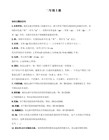
基于MSP430G2553的电压表设计
数字式直流电压表一、整体说明在电子技术中,往往离不开对电压的测量,作为一种测量电压的仪器——电压表是近代电子技术领域的常用工具之一,在许多领域得到广泛应用。
本设计是基于TI单片机设计的数字式直流电压表,它主要由MSP430G2553、LCD12864和分压电路三部分组成。
分压电路先将输入的电压信号衰减一定的倍数,后通过控制双路选择开关设定测量的量程,分别有0~3V和0~15V两个档,以便实现精确读数;分压处理后的电压信号由MSP430G2553内部的ADC10模块转换成数字信号;再通过LCD12864液晶屏进行串行显示。
经多次测量实验得出误差范围在2%以内。
二、原理图基于MSP430G2553单片机设计的数字式直流电压表的电路图如图1所示。
由于MSP430开发板已具备单片机最小系统结构,只需添加显示电路和分压电路。
LCD12864通过串口方式显示,只需占用单片机2个I/O口;分压电路可以通过开关S1选择量程档位,只占用1个I/O口。
图1 直流电压表电路图三、接口定义MSP430G2553的接口说明如表1所示。
图1中的复位和晶振部分是MSP430开发板固有的部分,故不再说明。
P1.0接液晶屏的SID脚,作为串行的数据口用;P1.1则接液晶屏的SCLK脚,控制串行的同步时钟;P1.4接分压电路的输出端。
LCD12864的接口说明如表2所示。
当PSB脚接低电平时,串口模式被选择。
在该模式下,只用2根线(SID与SCLK)来完成数据传输。
RS接高电平,不使用片选功能。
注意:信号源与单片机之间要共地。
表1 MSP430G2553的接口说明表2 LCD12864的接口说明四、程序流程图(一)主函数主函数的流程框图如图1所示。
主函数主要是调用系统初始化函数和循环开启ADC 转换,这是由于ADC10采用单通道单次转换模式,每次采样后需要重新开启ADC ,才会进行下一次信号采样转换。
另外,信号的采样与处理以及电压值的显示都是通过中断来完成。
MSP430G2553的UART与SPI应用
UTXE不会因SWRST 而更改。
ME1 |= UTXE0 + URXE0 //使能 USART0 TXD/RXD模块USART中特有的
使能配置。
IE1 |= URXIE0 //使能USART0 接收中断
10 P2.2
通用I/O 口、Timer1_A捕获CCI1B输入比较Out1输出
11 P2.3
通用I/O 口、Timer1_A捕获CCI0B输入比较Out0输出
12 P2.4
通用I/O 口、Timer1_A捕获CCI2A输入比较Out2输出
U0CTL |= CHAR; // 配置控制寄存器数据类型为8位。
U0TCTL |= SSEL0 // 选择时钟UCLK= ACLK。
U0BR0 = 0x45 // 分频系数的高8位8MHz 时钟下波特率为115200
(CPHA) 控制着两个 SPI 设备间何时数据交换以及何时对接收到的数据进行采样, 来保
证交换(Data Exchanges)
SPI 设备间的数据传输之所以又被称为数据交换, 是因为 SPI 协议规定一个 SPI
SPI 物理模块最终失效. 因此, 在程序中一般都会在 SPI 传输完数据后, 去读取 SPI 设
备里的数据, 即使这些数据(Dummy Data)在我们的程序里是无用的.
3、 工作机制
3.1. 概述
上图只是对 SPI 设备间通信的一个简单的描述, 下面就来解释一下图中所示的几个
测试数据输入或测试时钟输入
15 P1.7
通用I/O 口、ADC10模拟输入A7、Comparator_A+CA7输入、图
基本时钟模块_MSP430G2553

基本时钟模块_MSP430G2553G2xxx系列DCO校准数据(校正寄存器)1MHz:CALBC1_1MHZCALDCO_1MHZ8MHz:CALBC1_8MHZCALDCO_8MHZ12MHz:CALBC1_12MHZCALDCO_12MHZ16MHz:CALBC1_16MHZCALDCO_16MHZ例:设置DCO频率为1MHzif(CALBC1_1MHZ==0xFF || CALDCO_1MHZ==0xFF)while(1);//校准数据是否被擦除,若是则CPU挂起。
BCSCTL1 = CALBC1_1MHZ;DCOCTL = CALDCO_1MHZ;基本时钟模块寄存器寄存器缩写形式类型初始状态DCO控制寄存器DCOCTL 读/写0x60(PUC)基本时钟系统控制器1 BCSCTL1 读/写0x87(POR)基本时钟系统控制器2 BCSCTL2 读/写由PUC复位基本时钟系统控制器3 BCSCTL3 读/写0x05(PUC)中断使能寄存器(特殊功能寄存器)IE1 读/写由PUC复位中断标致寄存器(特殊功能寄存器)IFG1 读/写由PUC复位说明:DCO的频率可以通过软件设定DCOx、MODx、RSELx相应位来调整,DCO频率是通过将f DCO和f DCO+1混频得到。
1、DCOCTL:DCO控制寄存器7 6 5 4 3 2 1 0DCOx MODxrw-0 rw-1 rw-1 rw-0 rw-0 rw-0 rw-0 rw-0 DCOx:DCO频率范围选择位,这些位可以用来在由RESLx设置决定的8个离散的频率范围中选择哪一个。
MODx:调制系数选择位,这些位用来决定在32个DCO时钟周期中f DCO+1占多少个,f DCO 占多少个。
注意:当MODx=0时调制器关闭,DCOx=7时,由于此时没有下一个更高的频率范围f DCO+1可用,因此MODx无效不可用。
2、BCSCTL1:基本时钟系统控制寄存器17 6 5 4 3 2 1 0 XT2OFF XTS(1)(2)DIVAx RSELxrw-(1) rw-(0) rw-(0) rw-(0) rw-0 rw-1 rw-1 rw-1 XT2OFF:第二晶振XT2(可选高频晶振)关闭控制位。
msp430g2553串口通信
MSP430g2553串口通信MSP430的不同型号,其串行通讯工作模式是一样的。
以MSP430G2553为例进行说明。
MSP430G2553是20个引脚的16位单片机。
具有内置的16位定时器、16k 的FLASH 和512B 的RAM ,以及一个通用型模拟比较器以及采用通用串行通信接口的内置通信能力。
此外还具有一个10位的模数(A/D)转换器。
其引脚排布如图1.1所示。
其功能表如表1.1所示。
串行通讯模块主要由三个部分组成:波特率生成部分、发送控制器以及接收控制器。
如图1.2所示。
一、UART 模式在异步模式下,接收器自身实现帧的同步,外部的通讯设备并不使用这一时钟。
波特率的产生是在本地完成的。
异步帧格式由1个起始位、7或8个数据位、校验位(奇/偶/无)、1个地址位、和1或2个停止位。
一般最小帧为9个位,最大为13位。
图1.2 串行通讯模块内部结构图图1.1 MSP430G2553引脚图(一)UART的初始化单片机工作的时钟源来自内部三个时钟或者外部输入时钟,由SSEL1、SSEL0,以决定最终进入模块的时钟信号BRCLK的频率。
所以配置串行通讯的第一步就是选择时钟。
通过选择时钟源和波特率寄存器的数据来确定位周期。
所以波特率的配置是串行通讯中最重要的一部分。
波特率设置用三个寄存器实现:UxBR0(选择控制器0):波特率发生器分频系数低8位。
UxBR1(选择控制器1):波特率发生器分频系数高8位。
UxMCTL 数据传输的格式,以及数据传输的模式是通过配置控制寄存器UCTL来进行设置。
接收控制部分和发送控制部分。
首先需要串行口进行配置、使能以及开启中断。
串口接收数据一般采用中断方式,发送数据采用主动发送。
当接收到一个完整的数据,产生一个信号:URXIFG0=1(类似于51单片机的接收中断标志位),表示接收完整的数据。
当数据正在发送中,UTXIFG0=1,此时不能再发送数据,必须等当前数据发送完毕(UTXIFG0=0)才能进行发送。
103636_基于MSP430G2553的频率计设计
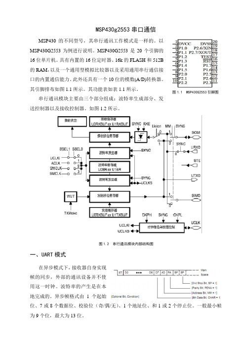
数字式频率计一、设计概述在电子技术中,频率是最基本的参数之一,数字频率计具有精度高、使用方便、测量迅速、以及便于实现测量过程自动化等优点,是近代电子技术领域的重要工具之一,在许多领域得到广泛应用。
本系统以超低功耗MSP430G2553单片机为核心处理芯片来测量信号的频率,通过定时器A 采用计数法完成信号频率测量,并将被测频率值通过LCD12864液晶串行显示。
频率可测量范围在1Hz 到999MHz 之间。
如需要,范围可继续扩宽,频率计的误差在1%以内。
二、原理图基于MSP430G2553的频率计设计原理图如图1所示,通过串口方式液晶显示,只需配置单片机三个口线便可以实现对频率的测量。
其中待测频率信号从P1.0口输入,然后可以直接在液晶屏上显示。
三、引脚说明(一)MSP430G2553引脚功能说明由原理图可以看出,430单片机的最小系统用到1脚电源、16脚复位端、20脚接地端、配置P1.0口为待测信号输入端,P1.4为串行数据输出口,P1.5为串行时钟输出口,如表1所示。
图1 基于MSP430G2553频率计设计原理图表1 MSP430G2553引脚功能说明引脚序号引脚名称功能说明备注1 VCC 电源正2 P1.0 频率信号输入端6 P1.4 串行数据输出端7 P1.6 串行时钟输出端16 RST 复位脚20 GND 电源地(二)LCD12864引脚功能说明LCD12864液晶显示屏用到1、2脚,电源接口线,19、20脚背光电源接口线,15脚并行/串行接口选择,5脚串行数据口,6脚串行的同步时钟。
LCD12864引脚功能如表2所示。
表2 LCD12864接口说明引脚序号引脚名称功能说明备注1 VSS 模块的电源地2 VDD 模块的电源正端4 RS(CS) 并行指令/数据选择信号;串行片选信号5 R/W(SID) 并行读写选择信号;串行的数据口6 E(CLK) 并行使能信号;串行的同步时钟15 PSB PSB并/串行接口选择:H-并行,L-串行19 LED_A 背光源正极20 LED_K 背光源负极(0V)四、软件设计流程图系统软件设计包括初始化模块、中断模块和信号频率显示模块。
单片机msp430g2553中文教程

24 TSSOP 封
LF,
装
-
1
DCO,
VLO
20 引脚
16 TSSOP 封
装
16
20 引脚 PDIP 封装
24
32 引脚 QFN 封装
28 引脚
24 TSSOP 封
LF,
装
-
1
DCO,
VLO
20 引脚
16 TSSOPyright © 2011–2012, Texas Instruments Incorporated
• 通用串行通信接口 (USCI) – 支持自动波特率检测的增强型通用异步收发器 (UART) – IrDA 编码器和解码器 – 同步 SPI – I2C™
• 用于模拟信号比较功能或者斜率模数 (A/D) 转换的 片载比较器
• 带内部基准、采样与保持以及自动扫描功能的 10 位 200-ksps 模数 (A/D) 转换器(见 表 1)
3
MSP430G2x53 MSP430G2x13
ZHCS178E – APRIL 2011 – REVISED JANUARY 2012
器件引出脚配置、MSP430G2x13 和 MSP430G2x53、20 引脚器件、 TSSOP 和 PDIP 封装
DVCC 1 P1.0/TA0CLK/ACLK/A0/CA0 2 P1.1/TA0.0/UCA0RXD/UCA0SOMI/A1/CA1 3 P1.2/TA0.1/UCA0TXD/PUCA0SIMO/A2/CA2 4 P1.3/ADC10CLK/CAOUT/VREF-/VEREF-/A3/CA3 5 P1.4/SMCLK/UCB0STE/UCA0CLK/VREF+/VEREF+/A4/CA4/TCK 6 P1.5/TA0.0/UCB0CLK/UCA0STE/A5/CA5/TMS 7
54MSP430 G2553 1(IO口及时钟A)
54MSP430 G2553 学习笔记一,MSP430G2553单片机的各个功能模块(一),IO口模块,1,我们所用的MSP430G2553有两组IO口,P1和P2。
2,IO口的寄存器有:方向选择寄存器PxDIR,输出寄存器PxOUT,输入寄存器PxIN,IO口内部上拉或下拉电阻使能寄存器PxREN, IO口功能选择寄存器PxSEL和PxSEL2,IO口中断使能寄存器PxIE,中断沿选择寄存器PxIES,IO口中断标志寄存器PxIFG。
3,所有的IO都带有中断,其中所有的P1口公用一个中断向量,所有的P2口公用一个中断向量。
所以在使用中断时,当进入中断后,还要判断到底是哪一个IO口产生的中断,判断方法可以是判断各个IO口的电平。
4,中断标志PxIFG需要软件清除,也可以用软件置位,从而用软件触发一个中断。
注意:在设置PxIESx时根据PxINx有可能会引起相应的PxIFGx置位(具体的情况见用户指南),所以在初始化完IO口中断以后,正式使用IO 中断前要先将对应的PxIFGx清零。
程序如下:void IO_interrupt_init() //IO中断初始化函数{P1REN |= BIT4+BIT5+BIT6+BIT7; // pullup 内部上拉电阻使能//使用中断时,使能内部的上拉电阻这样当该脚悬空时,电平不会跳变,防止悬空时电平跳变不停的触发中断 P1OUT = BIT4+BIT5+BIT6+BIT7; // 当引脚上的上拉或下拉电阻使能时,PxOUT选择是上拉还是下来//0:下拉,1:上拉P1IE |= BIT4+BIT5+BIT6+BIT7; // interrupt enabled P13中断使能P1IES |= BIT4+BIT5+BIT6+BIT7; // Hi/lo edge 下降沿中断//P1IES &= ~BIT3; //上升沿触发中断P1IFG &= ~(BIT4+BIT5+BIT6+BIT7); //中断标志位清零}5,PxOUT:如果引脚选择了内部的上拉或下拉电阻使能,则PxOUT设定电阻是上拉还是下拉,0:下拉,1:上拉 6,当IO口不用时,最好不要设为输入,且为浮动状态(这是IO口的默认状态),因为当输入为浮动时,输入电压有可能会在VIL和VIH之间,这样会产生击穿电流。
基于MSP430G2553的简易信号发生器

基于MSP430G2553的简易信号发生器浙江工业大学摘要:本作品基于TI的LaunchPad设计了一款简易信号发生器,选用TI的MSP430G2553单片机。
通过单片机加外围LCD12864、DAC0832及TL082放大电路,实现了可产生正弦波、锯齿波、三角波、方波的简易信号发生器,且频率可调。
关键词:MSP430G2553 DAC0832 正弦波锯齿波三角波一、作品基本功能介绍表1.1 技术参数2 在信号产生和处理方面。
通过MSP430G2553内部的TA 定时器,外加DAC0832产生四种波形,在DA 输出后,通过一个由运算放大器TL082和精密可调电位器组成的运算放大电路,以实现信号的增益控制。
最后在 50负载电阻上输出电压。
系统总体框图如图1.1所示。
图1.1系统总体框图表1.2 按键功能说明二、系统硬件和软件说明1 硬件构成本作品使用LCD12864作为人机交互模块,由于MSP430G2553的I/O 口很少,所以通过对LCD 的进行串行数据输入,以节约I/O 口。
其连接如图1.2所示。
+5V图1.2 LCD12864硬件连接由于是通过MSP430G2553输出数字量的信号来产生波形,因此需要用到DA 将数字量转换为模拟量。
考虑到单片机的I/O 口数量,选用8位的DA 来进行数模转换。
硬件如图1.3所示,DAC0832采用直通工作方式,节省I/O 口控制引脚。
+5V+5VI OUTP1.0-P1.3P1.4-P1.7图1.3 DAC0832 直通方式硬件连接由DAC 输出模拟量后,由于波形的幅值太小,因此还需要进行幅值的放大。
其中R3是精密可调电位器,方便用户对信号的幅度进行调节。
50Ω的电阻可以保证整个信号发生器的输出阻抗为50Ω。
信号幅度调节和输出部分电路如图1.4所示。
图1.4 幅值放大的硬件电路2 软件系统整个系统的软件主要有主函数、定时器TA 中断函数、按键中断函数三个大的模块组成。
MSP430G2553寄存器资料讲解

MSP430G2553学习笔记常用赋值运算符:清除:&=~ ,置位:|= ,测试:&= ,取反:^= ,看门狗模块:WDT(看门狗)WDTCTL 看门狗定时器控制寄存器15--8 7 6 5 4 3 2 1 0口令HOLD NMIES NMI TMSEL CNTCL SSEL IS1 IS0IS1,IS0 选择看门狗定时器的定时输出,T是WDTCNT的输入时钟源周期0 T x 2(15)1 T x 2(13)2 T x 2(9)3 T x 2(6)SSEL 选择WDTCNT的时钟源0 SMCLK1 ACLKIS0、IS1、SSEL可确定WDT定时时间,WDT只能定时8种和时钟源相关的时间WDT可选的定时时间(晶体为32768HZ,SMCLK=1MHZ)SSEL IS1 IS0 定时时间/ms0 1 1 0.056 Tsmclk x 2(6)0 1 0 0.5 Tsmclk x 2(9)1 1 1 1.9 Taclk x 2(6)0 0 1 8 Tsmclk x 2(13)1 1 0 16 Taclk x 2(9)0 0 0 32 Tsmclk x 2(15)(PUC复位后的值)1 0 1 250 Taclk x 2(13)1 0 0 1000 Taclk x 2(15)CNTCL当该位为1时,清除WDTCNTTMSEL 工作模式选择0 看门狗模式1 定时器模式NMI 选择RST/NMI引脚功能,在PUC后被复位0 RST/NMI引脚为复位端1 RST/NMI引脚为边沿触发的非屏蔽中断输入NMIES 选择中断的边沿触发方式0 上升沿触发NMI中断1 下降沿触发NMI中断HOLD 停止看门狗定时器工作,降低功耗0 WDT功能激活1 时钟禁止输入,计数停止WDT(看门狗)配置语句WDTCTL=WDTPW+WDTHOLD;//将WDTPW+WDTHOLD赋值给WDTCTL,关闭看门狗定时器控制寄存器(Stop watchdogtimer)IE1 |= WDTIE;//使能WDT中断WDTCTL = WDT_ADL Y_1000;//WDT 1 s / 4间隔计时器WDTCTL = WDTPW + WDTHOLD + WDTNMI + WDTNMIES;//WDTCTL 由高8位口令和低8位控制命令组成,要写入操作WDT的控制命令,出于安全原因必须先正确写入高字节看门狗口令。
msp430g2553nrf24l01(msp430g2553nrf24l01)
msp430g2553 nrf24l01(msp430g2553 nrf24l01)#包括“io430。
”#包括“API。
”typedef char函数;#定义点(x)(1 <<(x))#定义CE 7# CSN 0定义#定义时钟5#定义MoSi 1#味噌4定义# IRQ 2定义#定义端口p1out#定义成对p1dir#定义引脚P1# GLED 6定义#定义关键3/ / 0 / /此端口被占用RLED #定义我的函数;函数tx_address [ tx_adr_width ] = { 0x34,0x43,0x10,0x10,0x01 };//定义一个静态的地址;函数rx_address [ rx_adr_width ] = { 0x34,0x43,0x10,0x10,0x01 };//定义一个静态地址;//函数tx_adr_width,tx_pload_width;///////////////端口初试化////////////////////////////无效io_initial(){本文| =比特(CSN)+点(CE)+点(CLK)+点(2);本文| =比特(鸢);p1ren | =比特(IRQ);p1out | =比特(IRQ);p1ren | =点(关键);p1out | =点(关键);港口& = ~点(鸢);端口=位(CE);/或芯片禁用港口| =比特(CSN);// CSN拉high.disable操作端口=位(CLK);/时钟是低的}/ /*********************************************************** *******************************/ /延时函数/ /*********************************************************** *******************************无效delay_us(unsigned int n){为(n;0;n);}//////////////////初始化时钟虚空(void)FaultRoutine而(1);//异常挂起}configclocks虚空(void){如果(calbc1_1mhz = = 0xff | | caldco_1mhz = = 0xff)faultroutine();//如果校准数据擦除/ /运行faultroutine()bcsctl1 = calbc1_1mhz;//设置范围dcoctl = caldco_1mhz;//设置DCO步+调制bcsctl3 | = lfxt1s_2;// LFXT1 = VLOifg1 & = ~ ofifg;//清OSCFault旗bcsctl2 = 0;// MCLK SMCLK DCO = =}////////////// LED开启或关闭//////////////无效gled_off(){港口& = ~点(鸢);}无效gled_on(){港口| =比特(鸢);}无效gled_ray(){港口^ =比特(鸢);}///////////////得到IRQ //////////////////////// get_key函数(void){返回(引脚(位(键)));/////////////////////////读写操作/////////////////////////////////////spi_rw函数(函数的字节){bit_ctr函数;端口=(位(CLK));对于(bit_ctr = 0;bit_ctr<8;bit_ctr + +)/输出8位{如果(字节和0x80)港口| =点(2);其他的{港口& = ~(比特(MOSI));//输出“字节”,MSB 2}字节(byte << 1);/ /移一点到最高位..港口| =比特(CLK);//设置时钟高..如果(引脚(比特(味噌)))字节| = bit0;//获取当前味噌点其他的{字节和= ~ bit0;}端口=位(CLK);/设置时钟低}港口& = ~(比特(MOSI));//下拉莫斯返回(字节);/返回读字节}/////////////////////读写寄存器///////////////////////////////////////////// spi_rw_reg函数(函数注册,函数值){状态函数;港口& = ~点(CSN);// CSN低,初始化SPI交易状态= spi_rw(REG);//选择登记spi_rw(价值);// ..写它的价值..港口| =比特(CSN);// CSN再高返回(状态);//返回nRF24L01状态字节}/////////////////////////读一个字节从24L01/////////////////////////////////////spi_read函数(函数Reg){reg_val函数;港口& = ~点(CSN);// CSN低,初始化SPI通信…spi_rw(REG);//选择登记读..reg_val = spi_rw(0);// ..然后读registervalue 港口| =比特(CSN);// CSN高,终止的SPI通信返回(reg_val);//返回登记的价值}/////////////////////////读取RX的载荷,RX / Tx地址//////////////////////////spi_read_buf函数(函数的函数的函数注册,* pbuf,字节){函数的状态,byte_ctr;港口& = ~点(CSN);//设置CSN低,初始化SPI传输状态= spi_rw(REG);//选择登记写和读状态字节对于(byte_ctr = 0;byte_ctr <字节;byte_ctr + +)byte_ctr pbuf [ ] = spi_rw(0);/ / perform spi _ rw read bytes from nrf24l01port | = bits (csn); / / seen csn high againreturn (status); / / return nrf24l01 status byte}/ / / / / / / / / / / / / / / / / / / / / / / / / write tx payload, rx / tx address / / / / / / / / / / / / / / / / / / / / / / // / / / / / / / / /uchar spi _ write _ buf (uchar reg, uchar * pbuf, uchar bytes) {uchar status byte _ ctr;port & = ~ bits (csn); / / seen csn low practice spi tranactionstatus = spi _ rw (reg); / / select register to write to and read status bytefor (byte _ ctr = 0; byte _ ctr < bytes; byte _ ctr + +) / / then write all bytes in buffer (* pbuf)spi _ rw (* pbuf + +);port | = bits (csn); / / seen csn high againreturn (status); / / return nrf24l01 status byte}/ / * * * * * * * * * * * * * * * * * * * * * * * * * * * * * * * * * * * * * * * * * * * * * * * * * * * * * * * * * * * * * * * * * * * * * * * * * * * * * * * * * * * * * * * */ / nrf24l01初始化/ / * * * * * * * * * * * * * * * * * * * * * * * * * * * * ** * * * * * * * * * * * * * * * * * * * * * * * * * * * * * * * * * * * * * * * * * * * * * * * * * * * * * * * * * /practice _ nrf24l01 void (void){delay _ us (100);port & = ~ bits (ce);port | = bits (csn);port & = ~ bits (clk);spi _ write _ buf (write _ reg + tx _ addr, tx _ address, tx _ adr _ width); / / enter tx _ address two nrf24l01spi _ write _ buf (write _ reg + rx _ addr _ p0, tx _ address, tx _ adr _ width); / / rx _ addr0 same as tx _ adr for auto ack./ / spi _ write _ buf (wr _ tx _ pload, tx _ buf, tx _ pload _ width); / / enter data two tx payloadspi _ rw _ reg (write _ reg + a _ aa, 0x00); / / 禁止所有pipe 自动应答, 调试tx时spi _ rw _ reg (write _ reg + a _ rxaddr, 0x00); / / 禁止所有接受通道spi _ rw _ reg (write _ reg + setup _ retr, 0x00); / / 禁止自动重发spi _ rw _ reg (write _ reg + rf _ ch, 0); / / select rf channel 40spi _ rw _ reg (write _ reg + rx _ pw _ p0, rx _ pload _ width); / / 设置接收数据长度spi _ rw _ reg (write _ reg + rf _ setup, 0x07); / / tx _ pwr: 0dbm, data rate: 1mbps, lna: hcurrspi _ rw _ reg (write _ reg + config, 0x0e); / / seen pwr _ ip bits enable crc (2 bytes) & prim: tx. max _ rt & tx _ ds enabled...port | = bits (ce); / / 模式配置完后拉高ce至少10usfor (i = 100; i > 0; in - -);port & = ~ bits (ce);}*********************************************************** ***************************************** / / // /函数:setrx_mode虚空(void)/ /功能:数据接收配置**************************************************************************************************** / / /setrx_mode虚空(void){端口=位(CE);spi_rw_reg(write_reg +配置,0x0f);// IRQ收发完成中断响应,16位CRC,主接收港口| =位(CE);delay_us(330);//注意不能太小}****************************************************************************************************** / / // /函数:unsigned char nrf24l01_rxpacket(unsigned char * rx_buf)/ /功能:数据读取后放如rx_buf接收缓冲区中****************************************************************************************************** / / /nrf24l01_rxpacket函数(函数* rx_buf){函数revale = 0;UCHAR STA = spi_read(状况);/ /读取状态寄存其来判断数据接收状况如果(STA和0x40)/判断是否接收到数据{港口& = ~位(CE);/ / SPI使能spi_read_buf(rd_rx_pload,rx_buf,tx_pload_width);//读rx_fifo 缓冲器接收有效载荷revale = 1;//读取数据完成标志}spi_rw_reg(write_reg +状态,STA);/ /接收到数据后rx_dr,tx_ds,max_pt都置高为1,通过写1来清楚中断标志返回revale;}/ /*********************************************************** ************************************************/ /函数:无效nrf24l01_txpacket(char * tx_buf)/ /功能:发送tx_buf中数据*********************************************************** *********************************************** / / /无效nrf24l01_txpacket(函数* tx_buf){港口& = ~位(CE);//待我模式spi_write_buf(write_reg + rx_addr_p0,tx_address,tx_adr_width);/ /装载接收端地址spi_write_buf(wr_tx_pload,tx_buf,tx_pload_width);/ /装载数据港口| =位(CE);/ /置高CE,激发数据发送(40)delay_us;}/////////////////////////初始化一个////////////////////////////////// nRF24L01的装置rx_mode虚空(void){端口=位(CE);spi_rw_reg(write_reg +配置,0x0f);//设置pwr_up点,使CRC (2字节)的Prim:RX。
MSP430_g2553
时钟模块的控制寄存器
Power Up Clear,复位信号
// Setting the DCO to 1MHz if (CALBC1_1MHZ ==0xFF || CALDCO_1MHZ == 0xFF) while(1); BCSCTL1 = CALBC1_1MHZ; // Erased calibration data? Trap! // Set range
Agenda
1、Value Line 简介 2、Code Composer Studio 3、CPU及基本时钟系统 4、中断及通用IO 5、定时器及增强型WDT 6、低功耗优化设计 7、ADC10 及 Comparator_A+ 8、串行通信 9、Grace 10、电容式触摸按键解决方案
3.1 MSP430G2xx 结构
4.2 Vector Table
4.3 中断处理函数编程
#pragma vector=WDT_VECTOR __interrupt void WDT_ISR(void) { IE1 &= ~WDTIE; IFG1 &= ~WDTIFG; BUTTON_IE |= BUTTON; } //disable interrupt //clear interrupt flag //Debouncing complete
DCOCTL
= CALDCO_1MHZ;
// Set DCO step + modulation
3.6 VLO校准
在运行期间对VLO进行校准 定时器 Timer_A 时钟源采用校准的1MHz DCO 采用由VLO提供的ACLK/8进行上升沿捕获 fVLO = 8MHz/Counts 参考例程 (SLAA340)
MSP430G2553制作的自行车测度系统
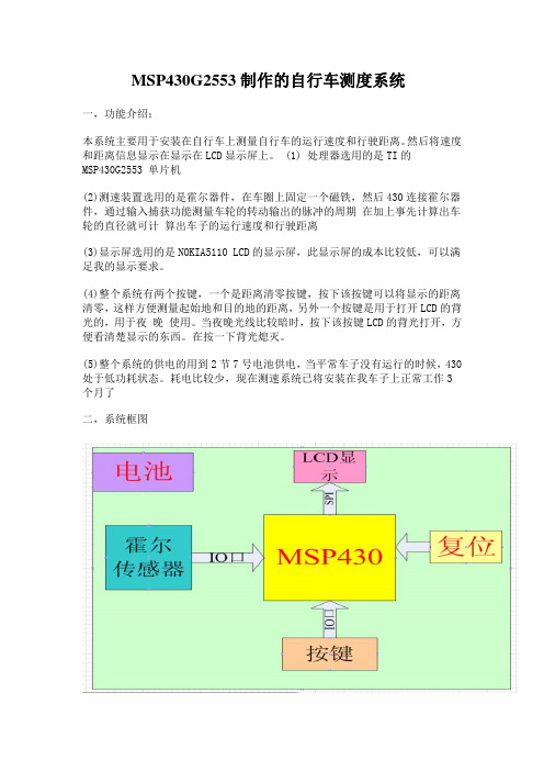
MSP430G2553制作的自行车测度系统一,功能介绍:本系统主要用于安装在自行车上测量自行车的运行速度和行驶距离。
然后将速度和距离信息显示在显示在LCD显示屏上。
(1) 处理器选用的是TI的MSP430G2553 单片机(2)测速装置选用的是霍尔器件,在车圈上固定一个磁铁,然后430连接霍尔器件,通过输入捕获功能测量车轮的转动输出的脉冲的周期在加上事先计算出车轮的直径就可计算出车子的运行速度和行驶距离(3)显示屏选用的是NOKIA5110 LCD的显示屏,此显示屏的成本比较低,可以满足我的显示要求。
(4)整个系统有两个按键,一个是距离清零按键,按下该按键可以将显示的距离清零,这样方便测量起始地和目的地的距离,另外一个按键是用于打开LCD的背光的,用于夜晚使用。
当夜晚光线比较暗时,按下该按键LCD的背光打开,方便看清楚显示的东西。
在按一下背光熄灭。
(5)整个系统的供电的用到2节7号电池供电,当平常车子没有运行的时候,430处于低功耗状态。
耗电比较少,现在测速系统已将安装在我车子上正常工作3个月了二,系统框图图1是整个系统的框图. LCD显示屏和MSP430G2553的连接采用的SPI接口,霍尔传感器和按键和430之间是IO口连接。
三,系统原理图图2是整个系统的原理图四,程序代码//******************************************************************* ***********#include#include#include#includeunsigned char Count, First_Time;unsigned int REdge1, REdge2, FEdge;unsigned char MST_Data, SLV_Data;#define DC P2OUT = P2OUT|(1<<5)#define SCE P2OUT = P2OUT|(1<<4)#define CLK_H P1OUT=P1OUT|(1<<5)#define CLK_L P1OUT=P1OUT&(~(1<<5))#define Data_H P1OUT=P1OUT|((1<<7))#define Data_L P1OUT=P1OUT&(~(1<<7))#define u8 unsigned char#define u16 unsigned inttypedef struct{u8 x;u8 y;}point;/*------5110屏幕尺寸和功能宏定义------*/#define DATA 1 //数据#define CMD 0 //命令#define LCD_X 84 //液晶屏横坐标宽度#define LCD_ROW LCD_X //液晶屏列宽度void LCD_write_byte(unsigned char dat, unsigned char command); void LCD_init(void);void LCD_init(void);void LCD_set_XY(unsigned char X, unsigned char Y);void LCD_clear(void);void LCD_write_char(unsigned char c);void LCD_write_String(unsigned char X,unsigned char Y,unsigned char *s); void LCD_write_byte(unsigned char dat, unsigned char command){unsigned int i;// LCD_SCE = 0; //5110片选有效,允许输入数据P2OUT &=~BIT4;if (command == 0) //写命令// LCD_DC = 0;P2OUT &=~BIT5;else // LCD_DC = 1;P2OUT |=BIT5;//写数据for (i=0;i<8;i++){CLK_L;//spi_clk=0;if((dat & 0x80)==0x80){Data_H;}else{Data_L;}CLK_H; // spi_clk=1;dat=(dat<<1);}P2OUT |=BIT4;}void LCD_init(void){P2OUT &=~BIT4;P1OUT &= ~BIT4;P1OUT |= BIT4;LCD_write_byte(0x21, 0); // LCD模式设置:芯片活动,水平寻址,使用扩展指令LCD_write_byte(0xc8, 0); // 设置液晶偏置电压LCD_write_byte(0x06, 0); // 温度校正LCD_write_byte(0x13, 0); // 1:48LCD_write_byte(0x20, 0); // 使用基本命令,V=0,水平寻址LCD_clear(); // 清屏LCD_write_byte(0x0c, 0); // 设定显示模式,正常显示P2OUT |=BIT4;}void LCD_set_XY(unsigned char X, unsigned char Y){LCD_write_byte(0x80 | X, 0); // X 行(横坐标)LCD_write_byte(0x40 | Y, 0); // column 列(纵坐标)}/*------------------------------------------//LCD_clear: LCD清屏函数--------------------------------------------*/void LCD_clear(void){unsigned char t;unsigned char k;LCD_set_XY(0,0);for(t=0;t<6;t++){for(k=0;k<84;k++){LCD_write_byte(0x00,1);}}}void LCD_write_char(unsigned char c){unsigned char i;c-=0x20; //ASCII码减去 0x20for (i=0; i<6; i++)LCD_write_byte(ASCII_6_8[c], 1);}void LCD_write_String(unsigned char X,unsigned char Y,unsigned char *s){LCD_set_XY(X,Y);while (*s) //等效*s!='\0'{LCD_write_char(*s);s++;}}static float speed;static unsigned char display[10];static unsigned char display2[10];static unsigned int temp ;static unsigned int distance=0;static float Period;static float Distance_km;int main(void){volatile unsigned int i;unsigned char lcd_buf[6][84];WDTCTL = WDTPW + WDTHOLD; // Stop watchdog timerP1DIR |= BIT0; // P1.0/LED OutputP1OUT &= ~BIT0; // LED offif (CALBC1_8MHZ==0xFF) // If calibration constant erased {while(1); // do not load, trap CPU!!}DCOCTL = 0; // Select lowest DCOx and MODx settingsBCSCTL1 = CALBC1_8MHZ; // Set DCO to 8MHzDCOCTL = CALDCO_8MHZ;P1DIR &= ~BIT2;P1SEL |= BIT2;P2DIR &= ~BIT2;P2DIR &= ~BIT1;P2IES |=BIT2+BIT1;P2IE |=BIT2+BIT1;P1DIR |= BIT0;P1DIR|=BIT4|BIT5|BIT7;TA0CCTL1 = CAP + CM_3 + CCIE + SCS + CCIS_0;TA0CTL |= TASSEL_1 + MC_2 + TACLR; // ACLK, Cont Mode; start timer Count = 0x0;First_Time = 0x01;P2OUT = 0x00;P2DIR |=BIT5+BIT4 ;P1DIR |=BIT4 ;_EINT();P1OUT &= ~BIT4; // Now with SPI signals initialized,P1OUT |= BIT4; // reset slaveLCD_init(); //初始化LCD模块LCD_clear(); //清屏幕LCD_write_String(0,1,"Speed:");LCD_write_String(60,1,"km/h");LCD_write_String(0,3,"Dista:");while(1){__bis_SR_register(LPM0_bits+GIE); // Enter LPM0 Period = REdge2 - REdge1; // Calculate Period speed = 1.0362*(32768/Period)*3.6;memset(display,0,sizeof(display));sprintf((char*)display,"%4.1f",speed);LCD_write_String(36,1," ");LCD_write_String(36,1,display);LCD_write_String(60,1,"km/h");LCD_write_String(50,3," ");Distance_km=(float)distance*2.073656/1000.0;if(Distance_km<1){LCD_write_String(34,3," ");Distance_km=Distance_km*1000;sprintf((char*)display2,"%d",(int)Distance_km); LCD_write_String(44,3,display2);}else{LCD_write_String(36,3," ");sprintf((char*)display2,"%6.3f",Distance_km); LCD_write_String(34,3,display2);LCD_write_String(72,3,"km");}}}// TA0_A1 Interrupt vector#pragma vector = TIMER0_A1_VECTOR__interrupt void TIMER0_A1_ISR (void){switch(__even_in_range(TA0IV,0x0A)){case TA0IV_NONE: break; // Vector 0: No interrupt case TA0IV_TACCR1: // Vector 2: TACCR1 CCIFG// distance++;if (TA0CCTL1 & CCI) // Capture Input Pin Status {distance++;if (!Count){REdge1 = TA0CCR1;Count++;}else{REdge2 = TA0CCR1;Count=0x0;__bic_SR_register_on_exit(LPM0_bits +GIE); // Exit LPM0 on return to main }if (First_Time)First_Time = 0x0;}else{if(!First_Time){FEdge = TA0CCR1;}}break;default: break;}}#pragma vector=PORT2_VECTOR__interrupt void PORT2 (void){unsigned int i;for(i=0;i<20000;i++);if(P2IFG&BIT1){distance=0;while(!(P2IN&BIT1));}if(P2IFG&BIT2){P1OUT=P1OUT^BIT0;while(!(P2IN&BIT2));}P2IFG=0x00;__bic_SR_register_on_exit(LPM0_bits +GIE); // Exit LPM0 on return to main }#define LCD_X 84 //液晶屏横坐标宽度#define LCD_ROW LCD_X //液晶屏列宽度。