ESD 保护 layout指南
电气设备的ESD防护指南
设备的ESD防护设计规范Reference to:1、IEC61000-4-2i目录1、目的 (1)2、范围 (1)3、术语和定义 (1)4、规范内容 (1)4.1 静电基础知识 (1)4.1.1静电的来源 (1)4.1.2 静电的特点 (1)4.1.3 静电放电的危害 (1)4.1.4 静电放电模型 (2)4.1.4.1 人体放电模型(Human-Body Model, HBM) (2)4.1.4.2 机器放电模型 (Machine Model, MM) (2)4.1.4.3 组件充电模型(Charged-Device Model, CDM) (4)4.2 设备的ESD防护设计要求 (5)4.2.1 整机结构设计 (5)4.2.2机箱设计 (7)4.2.3设备接地 (9)4.2.4电源线及I/O线 (10)5、相关记录 Records (11)6、附录Appendix (11)ii1、目的本规范的建立是为了给设备的设计和制造人员在设备的ESD防护设计方面提供相应的指导及必须遵循的规约。
2、范围适用于所有设备的设计和制造人员。
3、术语和定义静电:就是物体上多余的电荷积累,由相互摩擦或导体在静电场中感应产生。
ESD:即静电放电(Electro-Static Discharge),指带有不同静电电势的物体或表面之间的静电电荷转移,通过直接接触或电场击穿放电。
4、规范内容4.1静电基础知识4.1.1静电的来源a)摩擦剥离起电;b)绝缘体上堆积点电荷;c)静电场中导体感应起电;4.1.2静电的特点a)高电位:可达数万伏,操作时常达数百至数千伏(人通常对3KV以下静电无感知);b)瞬间大电流:产生瞬时脉冲电流的强度可达到几十安培;c)强电磁辐射:大电流脉冲,并产生强烈的电磁辐射,形成静电放电电磁脉冲,它的电磁能量往往会引起电子系统中敏感部件的损坏、翻转;d)作用时间短:微秒级或毫微秒级;e)受环境影响大:特别是湿度,湿度上升则静电积累减少,静电压下降;4.1.3静电放电的危害a)造成元器件失效,器件失效又分为突发性完全失效和潜在性缓慢失效;b)引起信息出错,逻辑电路翻转,导致设备故障;c)易吸附尘埃微粒,污染PCB板和半导体芯片;124.1.4 静电放电模型静电放电是一个复杂多变的过程。
ESD_layout
Signal Pad Layout(by Vic)Design rulePad项目使用的是tsmc80工艺,但是layout时主要是遵循tsmc90的rule,其中部分地方要参考tsmc80 none shrinkable的规则。
具体来说就是:design rule 有两个pdf文件,分别是90的rule和80的none shrinkable rule,在80文件中提到的none shrinkable的部分就按照80中尺寸要求来画,其他的都按照90中的要求画。
Pad introductionPad一般有signal pad和power pad两种,主要是用来做esd保护和作为芯片与外部的IO接口以及缓冲。
Pad layout在pad的layout中首先需要大致确定powerline,确定金属层的分配,对于pad 的宽度和高度都会有初步的估计和限制要求。
Powerline一般是由所有pad中最复杂的一个来决定的。
因为pad的layout结构都是细长型的,而且layout的结构化比较差,常常是原理图中一个完整的结构,到了layout中却分的很散,相隔比较远,因此连线就比较复杂。
Pad一般都有比较规律的hierarchy结构,top层一般有3个layout block:pwline、odev和dev。
Odev在下面,主要是esd管子和ODT的电阻部分,io从odev的最下面接入。
Dev是上面的控制电路,包括所有的数字控制部分和odt 以及buffer的其余电路。
Pwline主要用来作为各个pad之间的power和信号的连接。
ESD layout大尺寸的esd管子来做esd保护,同时在odev部分都有电阻和大管子做二级保护。
Esd管子基本上follow design rule中的规则来画,需要注意的地方:1、根据管子的类型和工作电压,design rule中有规定器件的w和l;2、注意esd管子的dummy(sdi和esd2dmy)层,以及rpo层的各个规则(包括带u上标的);3、二级esd保护管子没有rpo层,其他规则和普通esd管子一致;4、一排esd管子必须为偶数个,采用share drain端的形式;5、对于宽metal做45度倒角;6、 Drain端contact的数目和metal的宽度需要根据流经的ac和dc电流配合design rule中的公式来计算;7、 Guard ring的contact和管子的对齐;8、 80工艺中不同宽度的metal space要求不同,注意大于4.95um宽的metal 要有1.5um的space,drain端的metal要注意;9、注意IO大电流流经的metal的宽度;10、所有block最外面用接vpp的ring做保护连接;11、Mos管沟道到guard ring的距离,竖直距离为水平距离的1.5到2倍。
PCB layout的设计和抗ESD设计规则
电子设备中电路板布局、布线和安装的抗ESD设计规则在电子产品设计中必须遵循抗静电释放的设计规则,本文介绍静电释放(ESD)产生的原理,以及机箱、屏蔽层、接地、布线设计等诸多设计规则,它们有助于预防并解决静电释放产生的危害,值得中国电子设备设计工程师认真研究和学习。
许多产品设计工程师通常在产品进入到生产环节时才着手考虑抗静电释放(ESD)的问题。
如果电子设备不能通过抗静电释放测试,他们就会加班加点找寻不破坏原有设计的解决方案。
然而,最终的方案通常都要采用昂贵的元器件,还要在制造过程中采用手工装配,甚至需要重新设计,因此,产品的进度势必受到影响。
即使对经验丰富的工程师和设计工程师,也可能并不知道设计中的哪些部分有利于抗ESD。
大多数电子设备在生命期内99%的时间都处于一个充满ESD的环境之中,ESD可能来自人体、家具、甚至设备自身内部。
电子设备完全遭受ESD损毁比较少见,然而ESD干扰却很常见,它会导致设备锁死、复位、数据丢失和不可靠。
其结果可能是:在寒冷干燥的冬季电子设备经常出现故障现象,但是维修时又显示正常,这样势必影响用户对电子设备及其制造商的信心。
ESD产生的机理要防止ESD,首先必须知道ESD是什么以及ESD进入电子设备的过程。
一个充电的导体接近另一个导体时,就有可能发生ESD。
首先,两个导体之间会建立一个很强的电场,产生由电场引起的击穿。
两个导体之间的电压超过它们之间空气和绝缘介质的击穿电压时,就会产生电弧。
在0.7ns到10ns的时间里,电弧电流会达到几十安培,有时甚至会超过100安培。
电弧将一直维持直到两个导体接触短路或者电流低到不能维持电弧为止。
ESD的产生取决于物体的起始电压、电阻、电感和寄生电容:1.可能产生电弧的实例有人体、带电器件和机器。
2.可能产生尖峰电弧的实例有手或金属物体。
3.可能产生同极性或者极性变化的多个电弧的实例有家具。
ESD可以通过五种耦合途径进入电子设备:1.初始的电场能容性耦合到表面积较大的网络上,并在离ESD电弧100mm处产生高达4000V/m的高压。
ESD_layout
ESD_layoutSignal Pad Layout(by Vic)Design rulePad项目使用的是tsmc80工艺,但是layout时主要是遵循tsmc90的rule,其中部分地方要参考tsmc80 none shrinkable的规则。
具体来说就是:design rule 有两个pdf文件,分别是90的rule 和80的none shrinkable rule,在80文件中提到的none shrinkable 的部分就按照80中尺寸要求来画,其他的都按照90中的要求画。
Pad introductionPad一般有signal pad和power pad两种,主要是用来做esd 保护和作为芯片与外部的IO接口以及缓冲。
Pad layout在pad的layout中首先需要大致确定powerline,确定金属层的分配,对于pad 的宽度和高度都会有初步的估计和限制要求。
Powerline一般是由所有pad中最复杂的一个来决定的。
因为pad的layout结构都是细长型的,而且layout的结构化比较差,常常是原理图中一个完整的结构,到了layout中却分的很散,相隔比较远,因此连线就比较复杂。
Pad一般都有比较规律的hierarchy结构,top层一般有3个layout block:pwline、odev和dev。
Odev在下面,主要是esd管子和ODT的电阻部分,io从odev的最下面接入。
Dev是上面的控制电路,包括所有的数字控制部分和odt 以及buffer的其余电路。
Pwline主要用来作为各个pad之间的power和信号的连接。
ESD layout大尺寸的esd管子来做esd保护,同时在odev部分都有电阻和大管子做二级保护。
Esd管子基本上follow design rule中的规则来画,需要注意的地方:1、根据管子的类型和工作电压,design rule中有规定器件的w 和l;2、注意esd管子的dummy(sdi和esd2dmy)层,以及rpo层的各个规则(包括带u上标的);3、二级esd保护管子没有rpo层,其他规则和普通esd管子一致;4、一排esd管子必须为偶数个,采用share drain端的形式;5、对于宽metal做45度倒角;6、Drain端contact的数目和metal的宽度需要根据流经的ac 和dc电流配合design rule中的公式来计算;7、 Guard ring的contact和管子的对齐;8、80工艺中不同宽度的metal space要求不同,注意大于4.95um宽的metal 要有1.5um的space,drain端的metal要注意;9、注意IO大电流流经的metal的宽度;10、所有block最外面用接vpp的ring做保护连接;11、Mos管沟道到guard ring的距离,竖直距离为水平距离的1.5到2倍。
ESD静电控制手册(ESD手册中英文)

ESD静电控制手册TABLE OF CONTENTS1. Purpose 目的2. Scope 范围3. Definition 定义4. Responsibility 职责5. Operation Content 作业内容5.1 ESD Control Program ESD 管制方案5.2 ESD Control Program Mgr or Coordinator ESD 管制方案经理或协调员5.3 Update 文件修改与更新5.4 ESD Control Operation ESD 管制作业5.4.1 ESD Protected Area ESD 保护区5.4.2 Training Requirement 培训要求5.4.3 ESD Test requirements ESD 测试要求5.4.4 ESD Grounding System ESD 接地系统5.4.5 ESD Floor Control ESD 地板管制5.4.6 ESD Garment & ESD Cap Control 静电衣服&静电帽管制5.4.7 ESD Shoe Control 静电鞋管制5.4.8 ESD Gloves& Finger Cots Control 静电手套&指套管制5.4.9 ESD wrist strap Control 静电手环管制5.4.10 Equipment ESD Control 设备ESD 管制5.4.11 Fixture& Tools Control 工治具管制5.4.12 Work Surface control 工作台管制5.4.13 ESD Marking ESD 标示5.4.14 ESD Packaging Material ESD 包装材料管制5.4.15 ESD Seating 静电座椅5.4.16 Soldering Iron Control 铬铁静电管制5.4.17 Air Ionizer Control 离子风机管制5.5 Sub-contractor control 外包商管制6.Reference 参考文件ESD Manual 静电控制手册1. Purpose 目的To prevent ESDS objects in manufacture, assembly, install, package, test, inspection,preservation, transport or other operation activities from damage, and protect electrical or electronic parts, assemblies and equipment so as to guarantee the product quality, so ESD protection.为防止静电敏感元器件在生产、组装,安装,包装,测试,检验、保存、運送及其他活动中受到静电之损害,保护电子器件,组件和设备,从而保证产品品质,特制订此手册,以提供本公司静电防护之最高指引.2. Scope 范围Applicable to all the related activities from ESD objects in DXC适用于公司所有ESD 敏感物件之相关活动作业3. Definition 定义3.1 ESD-E lectro S tatic D ischarge, the transfer or movement of charge between objects that are at different electrical potentials by direct contact or induced by electrostatic field.ESD-静电释放,是指通过直接接触或静电场感应的方式,在不同电势差物体间的电荷转移或移动。
手持设备的ESD保护
手持设备的ESD保护一)ABSTRACT手持设备在其生产和使用过程中都会收到ESD的威胁,可能因此产生器件损坏、死锁、复位、信息丢失等问题,影响系统可靠性,而且随着器件的集成度的提高以及手持设备的小型化,ESD问题越来越需要足够的重视.本文详细论述了ESD的产生原因以及其对手持设备的危害,并介绍了IEC61000-4-2的标准和ESD测试的方法.ESD的防护方法很多,效果不一,在本文中我们对各种方法进行了详细的介绍,另外对于电路的布局也提供了相应的参考.本文针对目前的手持设备ESD防护的需求,重点介绍了串口/SIM卡/AUDIO/LCD等处的ESD防护技术.二)ESD产生的机理与对手持设备的危害两种不导电材料的接触与分离都会引起电子的转移,因而在各物体上产生额外的电荷。
当积累的静态电荷向另一个电位较低(相对地)的物体放电时,就产生了ESD。
在0.7ns到10ns的时间里,电弧电流会达到几十安培,有时甚至会超过100安培。
电弧将一直维持直到两个导体接触短路或者电流低到不能维持电弧为止。
放电量的大小和放电持续时间取决于充电材料的类型和周围的环境等多种因素。
所有的便携电子器件,从最基本的到最复杂的,都容易受到ESD 的损坏。
ESD基本上可以分为三种类型,一是各种机器引起的ESD,二是家俱移动或设备移动引起的ESD,三是人体接触或设备移动引起的ESD。
在手持设备中,人体引起的ESD是主要的因素。
ESD可以产生潜在的破坏电压、电流以及电磁场。
如果是直接接触系统的外部导电端,那么这个电压将直接进入系统内部,如果是空气放电的话,ESD电流产生的电磁场可以直接穿透设备或者通过孔洞、缝隙等耦合到敏感电路上。
当ESD放电电流在系统内部流动的时候,ESD 脉冲所导致的辐射波长从几厘米到数百米,这些辐射能量产生的电磁噪音将损坏或者骚扰它们的运行。
如果ESD感应的电压和/或电流超过电路的信号电平,电路的操作将失常.在高阻电路中,电流信号很小,此时电容耦合将占主导地位,ESD感应电压为主要问题,在低阻电路中,信号主要为电流形式,因而电感耦合占主导地位,ESD感应电流将导致大多数电路出现问题.因此实际系统中可能存在的ESD威胁可以归纳为4点:1)初始的电场能容性耦合到表面积较大的网络上,并在离ESD电弧100mm处产生高达4000V/m的高压。
静电保护(ESD)原理和设计

静电保护(ESD)原理和设计⼀直想给⼤家讲讲ESD的理论,很经典。
但是由于理论性太强,如果前⾯那些器件理论以及snap-back理论不懂的话,这个⼤家也不要浪费时间看了。
任何理论都是⼀环套⼀环的,如果你不会画鸡蛋,注定了你就不会画⼤卫。
静电放电(ESD: Electrostatic Discharge),应该是造成所有电⼦元器件或集成电路系统造成过度电应⼒(EOS: Electrical Over Stress)破坏的主要元凶。
因为静电通常瞬间电压⾮常⾼(>⼏千伏),所以这种损伤是毁灭性和永久性的,会造成电路直接烧毁。
所以预防静电损伤是所有IC设计和制造的头号难题。
静电,通常都是⼈为产⽣的,如⽣产、组装、测试、存放、搬运等过程中都有可能使得静电累积在⼈体、仪器或设备中,甚⾄元器件本⾝也会累积静电,当⼈们在不知情的情况下使这些带电的物体接触就会形成放电路径,瞬间使得电⼦元件或系统遭到静电放电的损坏(这就是为什么以前修电脑都必须要配戴静电环托在⼯作桌上,防⽌⼈体的静电损伤芯⽚),如同云层中储存的电荷瞬间击穿云层产⽣剧烈的闪电,会把⼤地劈开⼀样,⽽且通常都是在⾬天来临之际,因为空⽓湿度⼤易形成导电通到。
那么,如何防⽌静电放电损伤呢?⾸先当然改变坏境从源头减少静电(⽐如减少摩擦、少穿⽺⽑类⽑⾐、控制空⽓温湿度等),当然这不是我们今天讨论的重点。
我们今天要讨论的时候如何在电路⾥⾯涉及保护电路,当外界有静电的时候我们的电⼦元器件或系统能够⾃我保护避免被静电损坏(其实就是安装⼀个避雷针)。
这也是很多IC设计和制造业者的头号难题,很多公司有专门设计ESD的团队,今天我就和⼤家从最基本的理论讲起逐步讲解ESD保护的原理及注意点,你会发现前⾯讲的PN结/⼆极管、三极管、MOS管、snap-back全都⽤上了。
正向导通反向截⽌(不记得就去翻前⾯的课程),⽽且反偏电压继续增加会发⽣雪崩击穿(Avalanche Breakdown)⽽导通,我以前的专题讲解PN结⼆极管理论的时候,就讲过⼆极管有⼀个特性:正向导通反向截⽌们称之为钳位⼆极管(Clamp)。
GGNMOS(grounded-gate NMOS)ESD保护结构原理说明

IC设计小镇:收集整理GGNMOS(grounded-gate NMOS)ESD保护结构原理说明在早期的ESD 保护方案中,这种反接在电源间的diode 结构被广泛应用。
正向连接的diode 可以更好的处理大电流传输,但由于其较低的正向启动点压(6.5V),这样就限制了其在较高电源电平的电路中的应用。
多极串联diode(正向或者反向)可以解决这个问题,但是,同时由于其阻抗的增加减弱了其电流处理能力。
用大尺寸的diode 提高ESD 保护性能的同时会产生更多的寄生效应。
目前I/O 中还添加了应用广泛的ggNMOS(grounded-gate NMOS)ESD 保护结构,Drain 端接至PAD,Gate 端接至电源地。
ESD 保护利用其寄生的NPN三极管,形成一个低阻抗的放电通路,以此来保护IC 的内部电路。
如下图所示GGNMOS静电保护的工作原理GGNMOS 的剖面结构如下当PAD 端聚集大量的负电荷时,通过Drain 端与P-substrate 之间的PN 结,IC设计小镇:收集整理电荷由 B 端泻放到GND。
当PAD 端聚集大量的正电荷时,利用的是寄生的三极管。
寄生三极管的启动原理如下说明。
1、大量的正电荷聚集在Drain 端,一定的正电荷通过Drain 和P-substrate之间反偏的PN 结转移至Psubstrate,这部分正电荷聚集到同为P 型材料的 B 端,转移到GND。
如下图所示2、3、聚集到 B 端的正电荷,使得与Source 端的PN 结导通,由此导通寄生的三极管。
如下图所示寄生的三极管被打开,大量的正电荷通过Gate 下面的区域迅速由Drain 端转移到Source 端。
聚集的正电荷得以快速的泻放到地。
如下图所示在GGNMOS 结构的ESD 保护中,器件的的不均匀性将影响到其性能,在layoutIC设计小镇:收集整理的时候需要充分考虑到这个问题,同时可对器件进行改进,增加Drain 端的宽度,在电路中相当于添加小电阻,减小电流,提高其均匀性。
电子通讯设备ESD防护设计规范和指南
四.1
对于设备级的ESD防护设计,其重点应放在为静电放电设置一条通畅的泄放通道。主要应做好以下几点:
1.机箱金属之间要实现良好搭接。搭接处要采用面接触,避免点接触。搭接的直流电阻不大于2.5 ,整体搭接结构中任意两导电点间的直流电阻不大于25 。相互搭接的金属之间的电化学位差不大于0.6V。
19.对于输入输出接口处信号插针与金属外壳的隔离距离达不到5mm的接插件,其金属外壳附近应尽可能敷设大面积覆铜地线。接插件金属部分应与机壳用最短的接地线相连。
20.在复位信号线靠近复位按钮的输入端与地之间,以及靠近复位芯片的输入端与地之间分别并接0.1uF的陶瓷电容;复位线应尽可能短(小于3cm为宜)而宽(大于1mm为宜)。
人体由于自身的动作以及与其它物体的接触、分离、磨擦或感应等因素,可以带上几千伏甚至上万伏的静电。在干燥的季节,人们在黑暗中脱化纤衣服时,常常会听到“啪啪”的声音,同时还会看到火花,这就是人体的静电放电现象。在工业生产中,人是主要的静电干扰源之一。
一.2
1、静电放电是高电位,强电场,瞬时大电流的过程
大多数情况下静电放电过程往往会产生瞬时脉冲大电流,尤其是带电导体或手持小金属物体的带电人体对接地体产生火花放电时,产生的瞬时电流的强度可达到几十安培甚至上百安培。
⑵潜在性缓慢失效:器件受到ESD造成轻微损伤,器件的性能劣化或参数指标下降而成为隐患,使该电路在以后的工作中,参数劣化逐渐加重,最终失效。概率约90%。
三.2
ESD会在设备各处产生一个幅值为几十伏的干扰脉冲,引起信息出错,导致设备的故障;ESD也可产生频带几百千赫~几十兆赫、电平高达几十毫伏的电磁脉冲干扰,当脉冲干扰耦合到敏感电路时,也会引起信息出错,导致设备的故障。
ESD保护版图设计

摘要静电放电(简写为ESD)是集成电路(简写为IC)在制造、运输、以及使用过程中经常发生并导致IC芯片损坏或失效的重要原因之一。
工业调查表明大约有40%的IC失效与ESD/EOS(过强的电应力)有关。
因此,为了获得性能更好更可靠的IC芯片,对ESD开展专门研究并找到控制方法是十分必要的。
随着芯片尺寸的持续缩小,ESD问题表现得更加突出,已成为新一代集成电路芯片在制造和应用过程中需要重视并着力解决的一个重要问题。
论文论述了CMOS集成电路ESD 保护的必要性,研究了在CMOS电路中ESD 保护结构的设计原理,分析了该结构对版图的相关要求,重点讨论了在I/O电路中ESD 保护结构的设计要求。
论文所做的研究工作和取得的结果完全基于GGNMOS的器件物理分析,是在器件物理层次上研究ESD问题的有益尝试;相对于电路层次上的分析结果,这里的结果更加准确和可靠,可望为GGNMOS ESD保护器件的设计和制造提供重要参考。
关键词:静电放电(ESD);接地栅NMOS;保护器件;电源和地AbstractThe electrostatic discharge (ESD) is integrated circuit (IC) in manufacturing, transportation, and use process occurs frequently and cause IC chips damage or failure of one of the important reasons. Industrial survey shows that about 40 percent of IC failure and ESD/EOS (overpowered electrical stress) relevant. Therefore, in order to obtain better performance more reliable IC chips, to carry out special research and find the ESD control method is very necessary. Along with the continuous narrowing, chip size behaved more prominent ESD problems, has become a new generation of integrated circuit chip in the manufacture and application process needed to pay attention to and addressing an important question.This paper discusses the CMOS integrated circuit, the necessity of ESD protection in CMOS circuit was studied in the structure of ESD protection design principle, analyzes the structure on the map the relevant requirements, especially discussed in the I/O circuit ESD protection structure design requirements.Keywords:Electrostatic Discharge, GND gate NMOS, Protected Device, Power and Ground目录摘要 (1)Abstract (2)第1章绪论 (4)1.1 集成电路的发展状况 (4)1.1.1 集成度的提高 (4)1.1.2 摩尔定律 (4)1.2 集成电路中的ESD保护 (5)1.2.1 为何出现ESD (5)1.2.2 ESD保护的必要性 (5)第2章关于版图设计与版图设计环境的介绍 (7)2.1 集成电路版图设计 (7)2.2 版图结构 (7)2.3 版图设计流程与方法 (8)2.4 版图设计环境 (8)2.4.1 Technology file 与Display Resource File 的建立 (9)2.4.2 Virtuoso工具的使用 (9)第3章CMOS电路的ESD保护结构版图设计 (13)3.1 CMOS电路中ESD测试 (13)3.2 ESD保护原理 (14)3.3 CMOS电路ESD保护结构的设计 (14)3.3.1 CMOS电路ESD保护器件 (15)3.4 CMOS电路ESD保护结构的版图设计 (16)3.4.1 版图设计原则 (16)3.4.2 ESD保护结构版图设计 (17)第4章结束语 (18)参考文献 (19)致谢 (20)第1章绪论1.1 集成电路的发展状况1.1.1 集成度的提高真正导致数字集成电路技术发生革命性变化的是半导体存储器和微处理器的引入。
电源ESD以及芯片layout
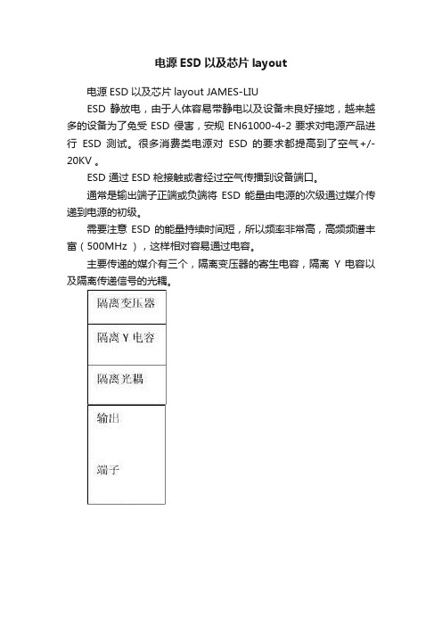
电源ESD以及芯片layout电源ESD 以及芯片layout JAMES-LIUESD 静放电,由于人体容易带静电以及设备未良好接地,越来越多的设备为了免受ESD 侵害,安规EN61000-4-2要求对电源产品进行ESD 测试。
很多消费类电源对ESD 的要求都提高到了空气+/-20KV 。
ESD 通过ESD 枪接触或者经过空气传播到设备端口。
通常是输出端子正端或负端将ESD 能量由电源的次级通过媒介传递到电源的初级。
需要注意ESD 的能量持续时间短,所以频率非常高,高频频谱丰富(500MHz ),这样相对容易通过电容。
主要传递的媒介有三个,隔离变压器的寄生电容,隔离Y 电容以及隔离传递信号的光耦。
ESD 通常不能通过的原因,也是因为一些距离不足,高压产生火花,或有高电压脉冲进入元件,从而造成元件损坏。
因此我们总是要注意一些元件以及走线的距离。
另外ESD 能量总是走阻抗最低的路径,你需要引导它到此路径上来时,就需要做到该线路阻抗比别的线路低。
比如放电针的针尖。
【隔离器件】,隔离变压器一般做好绝缘处理,不容易产生火花。
但也要注意裸露在外的磁芯与周围的一些距离。
光耦初次级的间距一定要比跨接的Y 电容的间距要大(Y 电容距离不够可开槽),否则就容易在光耦上产生火花。
此火花产生的脉冲很容易通过FB 进入芯片,造成芯片损坏。
因此唯一允许泄放的设计通道是将ESD 能量在Y 电容处完全泄放。
需要在Y 电容处设计放电针来实现。
放电针可以并排2,3组。
由于尖端放电的能量最强,所以对应的针尖要对齐。
由于安规距离的限制,最小距离控制在6.5mm 。
【次级回路】layout 上需考虑的就是输出端正,负的走线到初次级Y 电容的阻抗越小越好。
有的甚至正端的走线加放电针与Y 电容放电针并排。
常遇到431的地与输出地连成一片,而地与Y 电容距离较远,那么ESD 能量就容易引入到431,造成431损坏。
另外次级整流管的走线不能被地包围,否则也容易导致二极管损坏。
Layout(集成电路版图)注意事项及技巧总结材料
Layout(集成电路版图)注意事项及技巧总结材料Layout主要工作注意事项●画之前的准备工作●与电路设计者的沟通●Layout 的金属线尤其是电源线、地线●保护环●衬底噪声●管子的匹配精度一、l ayout 之前的准备工作1、先估算芯片面积先分别计算各个电路模块的面积,然后再加上模块之间走线以及端口引出等的面积,即得到芯片总的面积。
2、Top-Down 设计流程先根据电路规模对版图进行整体布局,整体布局包括:主要单元的大小形状以及位置安排;电源和地线的布局;输入输出引脚的放置等;统计整个芯片的引脚个数,包括测试点也要确定好,严格确定每个模块的引脚属性,位置。
3、模块的方向应该与信号的流向一致每个模块一定按照确定好的引脚位置引出之间的连线4、保证主信号通道简单流畅,连线尽量短,少拐弯等。
5、不同模块的电源,地线分开,以防干扰,电源线的寄生电阻尽可能较小,避免各模块的电源电压不一致。
6、尽可能把电容电阻和大管子放在侧旁,利于提高电路的抗干扰能力。
二、与电路设计者的沟通搞清楚电路的结构和工作原理明确电路设计中对版图有特殊要求的地方包含内容:(1)确保金属线的宽度和引线孔的数目能够满足要求(各通路在典型情况和最坏情况的大小)尤其是电源线盒地线。
(2)差分对管,有源负载,电流镜,电容阵列等要求匹配良好的子模块。
(3)电路中MOS管,电阻电容对精度的要求。
(4)易受干扰的电压传输线,高频信号传输线。
三、layout 的金属线尤其是电源线,地线1、根据电路在最坏情况下的电流值来确定金属线的宽度以及接触孔的排列方式和数目,以避免电迁移。
电迁移效应:是指当传输电流过大时,电子碰撞金属原子,导致原子移位而使金属断线。
在接触孔周围,电流比较集中,电迁移更容易产生。
2、避免天线效应长金属(面积较大的金属)在刻蚀的时候,会吸引大量的电荷,这时如果该金属与管子栅相连,可能会在栅极形成高压,影响栅养化层质量,降低电路的可靠性和寿命。
当代手机各外部接口的ESD保护设计指南
当代手机各外部接口的ESD保护设计指南在考虑为手机的ESD保护选择ESD保护元件之前,理解今天电子行业正在发生的一个关键趋势是非常重要的。
简言之,包含在今天各种应用采用的许多芯片组中的ESD保护电路数量正在减少。
换言之,这些芯片组在严重的、用户生成的ESD事件下免受损坏的能力正在下降。
目前几乎所有的芯片组都有片上ESD保护。
ESD电路放在芯片的外围和邻近I/O焊垫处,它用于在晶圆制造和后端装配流程中保护芯片组。
在这些环境中,ESD可通过设备或工厂的生产线工作人员引入到芯片组上。
关键的ESD规范包括人体模型(HBM)、带电器件模型(CDM)和机器模型(MM)。
这些测试规范的目的是确保芯片组在制造环境中维持很高的制造良率。
传统上,芯片制造商一直试图维持HBM要求的2,000V水平。
从成本效益比的角度来看,这已经被证明是件很难做到的事。
从图1可以看出,随著制造技术转向90nm以下,将ESD保护水平维持在2,000V的成本,已开始以指数级上升。
因此,现在新的目标是降低芯片上的ESD保护水平,但维持相同的高制造良率水平。
目前普遍接受的关键ESD保护电压水平约为500V。
在这一水平,芯片成本增加得较合理,良率水平也不会受到损害。
这是因为典型的晶圆厂和装配车间有将ESD限制在500V或以下的政策。
因此,即使所有的芯片组在裸片上包含一些ESD保护电路,其目的也只是确保制造的高良率。
不过,这一级别的ESD保护不足于保护芯片组免受消费者实际使用手机时将会碰到的严重ESD事件的伤害。
在无法预先控制的消费环境中,必须使用不同的ESD保护规范。
这就是IEC61000-4-2。
该IEC规范已被许多应用制造商(手机、智能电话、MP3播放器等)使用来确保其产品可靠地工作,以及不会遭受早期失败。
这一规范的ESD保护电压水平高很多,因此与HBM不兼容。
HBM规范要求的测试集中在500V。
另一方面,IEC中的空气放电方法要求的测试可以超过15,000V。
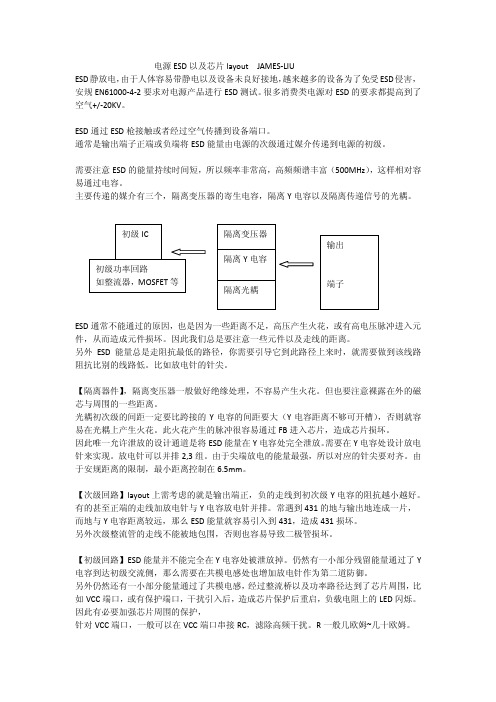
ESD防护指南说明书
APPLICATION GUIDE ESD PROTECTION介面INTERFACEHDMI 1.4HDMI 2/UHD/4KFlex Ray e SATACANBUSCONTROL IOS100MBETHERNET1G 10GPOE/POEPT1/E1-T3/E3USB 2.0USB 3.0USB 3.1USB 3.2XDSLLVDSLINBUS RS-232RS-485SMART BATTERYCOMMUNICATION APPLICATIONSESD Protection Solutions for High Speed Communication Ports• Electrostatic discharge (ESD) occurs when a charge is exchanged between two objects of unequal charge potential. ESD most often occurs between people and metal objects.It is a result of an electron build-up behaving as capacitor when dielectric isolation is available. Manmade materials, such as shoe soles, achieve dielectric isolation while someone walks on carpet creating kinetic energy. The potential threat of an ESD transient poses a challenge to system designers to incorporate overvoltage protection. Often,the included protection must have capacitance while not degrading the transmission rate. Traditionally,the use of a high capacitor was used to provide protection. However,due to high speed requirements, the capacitance perline must be significantly reduced. It must be done while still providing overvoltage protection against potential threats. Threats can include ESD, electrical fast transients (EFT), or surges. This paper discusses standard requirements for ESD. It highlights overvoltage protection solutions for the most common high speed interfaces. These include USB,HDMI and Ethernet ports, as shown in Table 1.Application Data Rate Capacitance RS-2320.20 Mbit/S< 50 pFT1 1.544 Mbit/S< 30 pF E2 2.048 Mbit/SI2C 3.4 Mbit/SEthernet10 Mbit/SUSB1.112 Mbit/S< 20 pF E334.368 Mbit/SRS-48535 Mbit/ST344.736 Mbit/SFast Ethernet100 Mbit/S< 5 pF T5400.352 Mbit/S< 3 pF USB 2.0480 Mbit/SE5565.148 Mbit/SIEEE-1394b786.432 Mbit/SGigabit E565.148 Mbit/SDVI3960 Mbit/S< 1 pF USB 3.05000 Mbit/SDisplayPort5400 Mbit/SSATA 3.06000 Mbit/SHDMI 1.310200 Mbit/SHDMI 2.010800 Mbit/S• CANPart No.V RWM P PK , 8/20uS C J , Max.ESD Level Package FSSU24T23A 24V 350 Watts 45 pF 30KV SOT -23FDA2431T 24V 230 Watts 30 pF 30KV SOT -23SOT24C 24V 160 Watts 50 pF 30KV SOT -23FM7127V / 12V400 Watts75 pF30KVSOT -23CMC optionalC M C L i n eSPLIT CANHCAN XceiverCANHESD ProtectionCAN system architecture with a single device to protect the CAN node• LINPart No.V RWM P PK , 8/20uS C J , Max.ESD Level Package ESD1524VD15V/24V160 Watts20 pF30KVSOD-323LIN system architecture with a single device to protect the LIN nodeVBATLINLIN XceiverGNDESD1524VDC MASTER/SLAVEL I N C o n n e c t o r• FlexRayPart No.V RWM P PK , 8/20uS C J , Max.ESD Level Package BSD24C 24V 350 Watts 50 pF 30KV SOD-323FSD24C 24V 350 Watts 50 pF 30KV SOD-323GBLC24CI 24V 350 Watts 0.6 pF 30KV SOD-323GBLC24C24V350 Watts0.6 pF30KVSOD-323Bi-directional and Uni-directional ESD protection for GRIOGPIO Bi-directional protection I/O pin GPIO Uni-directional protectionI/O pin• Car infotainmentPart No.V RWM P PK , 8/20uS C J , Max.ESD Level Package FW0524LCA5V150 Watts0.4 pF30KVDFN2510-10LIn LVDS systems, the FWO524LCAprovids ultra high-speed ESD protection that is fully AEC-Q101 compliantFW0524LCACentral boardModule board e.g.camera or displayUTP cable• Digital I/OPart No.V RWM P PK , 8/20uS C J , Max.ESD Level Package FLC052AD 5.0V 80 Watts 0.3 pF 25KV DFN0603FLC0529D 5.0V 40 Watts 0.3 pF 22KV DFN1006FLC052XD 5.0V 40 Watts 0.15 pF 22KV DFN0603FLC032XD 3.3V 45 Watts 0.20 pF 20KV DFN0603FHC2511D 2.5V 90 Watts 2.50 pF 30KV DFN1006FHC1815D1.8V200 Watts1.50 pF30KVDFN1006Bi-directional and uni-directional ESD protection for GPIOGPIO Bi-directional protection I/O pin GPIO Uni-directional protectionI/O pinSerial Buses• Legacy: RS-232 and RS-485Part No.V RWM P PK , 8/20uS C J , Max.ESD Level Package SOT12CB 12 V 180 Watts 40 pF 30KV SOT -23SOT15C15 V160 Watts30 pF30KVSOT -23Standard serial port, RS-485, or RS-23 protection can be either unidirectional or bidirectionalTransceiver 0-10 Ohm SOT15C Transceiver0-10 OhmSOT15CTransceiver0-10 OhmSOT12CB• Dual USB 2.0 ProtectionPart No.V RWM P PK , 8/20uS C J , Max.ESD Level Package FW0524LCA5V150 Watts0.4 pF30 KVDFN2510-10LVBUS 1. VBUS 2. D+3. D-4. GND1. VBUS2. D+3. D-4. GNDD1+D1-VBUS DUAL USB HOST.O applicationD1+D1-FW0524LCA• High data-rate: USB 3.0Part No.V RWM P PK , 8/20uS C J , Max.ESD Level Package FW4120LC 5V 150 Watts 0.4 pF 30KV DFN4120-10L FSD052MD5V45 Watts13 pF8KVDFN1006USB 3.0 ESD protectionVBUS USB 3.0TRANSCEIVERSSTX+SSTX-SSRX+SSRX-VBUS D+D-SSTX+SSTX-SSRX+SSRX-GNDD1+D1-FW4120LCFSD052MD• High data-rate: USB 3.1Part No.V RWM P PK , 8/20uS C J , Max.ESD Level Package FLC0529D 5 V 40 Watts 0.15 pF 22 KV DFN1006FDA0531D5 V100 Watts0.40 pF17 KVDFN1006-3LPart No.V RWM P PK , 8/20uS C J , Max.ESD Level Package FSD052MD 5 V 40 Watts 0.3 pF 30 KV DFN1006FW56 Series3.3 V– 20 V>300 Watts35 pF-600 pF30 KVDFN16102121123A 1A 2A 3A 4A 5A 6A 7A 8A 9A 10A 11A 12Super Speed Lines Super Speed Lines Super Speed Lines Super Speed Lines Power 5-20v Config Control Side band 2USB 2.0USB 2.0Side band 2Config Control Power 5-20v Super Speed Lines Super Speed Lines Super Speed Lines Super Speed LinesB 12B 11B 10B 9B 8B 7B 6B 5B 4B 3B 2B 1• High data-rate: eSATAPart No.V RWM P PK , 8/20uS C J , Max.ESD Level Package FW0524LCA5 V150 Watts0.4 pF30 KVDFN2510-10LGND A+A-GND B-B+GNDFW0524LCAeSATA connector• High-speed differential mode signalingPart No.V RWM P PK , 8/20uS C J , Max.ESD Level Package FW0524LCA5 V150 Watts0.4 pF30 KVDFN2510-10LGeneral high-speed differential mode signaling line ESD protectionFW0524LCAFW0524LCATX+TX-RX+RX-RX+RX-TX+TX-TP cableFESD0518LCDHDMI Type-AConnectorD2+GNDD2-D1+GNDD1-D0+GNDD0-CLK+GNDCLK-CECN/C (or HEC_DAT)SCLSDAGND5VHPD (or HEC_DAT)Display Interfaces• HDMI-Type APart No.V RWM P PK, 8/20uS C J, Max.ESD Level Package FESD0518LCD 5 V150 Watts0.4 pF30 KV DFN5515-18LDisplay Interfaces• PHY side in GbePart No.V RWM P PK, 8/20uS C J, Max.ESD Level Package FW0524LCA 5 V150 Watts0.4 pF30 KV DFN2510-10LFW0524LCAFW0524LCATPOPATPONATPOPBTPONBTPOPCTPONCTPOPDTPONDETHERNETTRANSCEIVERQUADTRANSCEIVERRJ45TRANSCEIVER• Gbe ModePart No.V RWM P PK , 8/20uS C J , Max.ESD Level Package FSRV05-45 V350 Watts1.2 pF30 KVSOT23-6Magnetics1/2 FSRV05-4PHY O/PTX O/P RJ45Magnetics 1/2 FSRV05-4PHY I/PRX I/P RJ45Gbe common modeMagnetics1/2 FSRV05-4PHY I/PRX I/PRJ45Gbe Differential mode Magnetics1/2 FSRV05-4PHY O/PTX O/P RJ45Magnetics1/2 FSRV05-4PHY I/PRX I/P RJ45Gbe Differential mode• Gbe ModeDisplay Interfaces• Gbe ModePart No.V RWM P PK, 8/20uS C J, Max.ESD Level Package FSRV05-45V350 Watts 1.2 pF30 KV SOT23-6 FLC03-3.3 2.8 V2500 Watts12 pF30 KV SOP-8FLC03-3.3FLC03-3.3FLC03-3.3FLC03-3.3FW0524LCAFW0524LCATPOPATPONATPOPBTPONBTPOPCTPONCTPOPDTPONDETHERNETTRANSCEIVERQUADTRANSCEIVERRJ45TRANSCEIVERAudio Circuit protectionPart No.V RWM P PK , 8/20uS C J , Max.ESD Level Package FLC052TDQ5 V80 Watts0.3 pF25 KVDFN1006Description:Audio jacks and connectors can present an entrypoint for ESD to enter the system. Audio signals do not typically exceed ± 5 V before amplification but can reach higher voltages after the amplifier. Since the maximumfrequency does not exceed 30 kHz, the capacitance of the ESD diode is not a concern. Because analog audio can have both positive and negative voltage swings, ESD solutions should be bidirectional to prevent premature breakdown which would interfere with the signal.RR AudioR Audio INGNDGNDAudio Amplifier Class AB (ESD Sensitive)Speaker Connector (Source of ESD)LL AudioL Audio INGNDAudio Amplifier Class AB (ESD Sensitive)Gb Ethernet Surge and ESD ProtectionPart No.V RWM P PK , 8/20uS C J , Max.ESD Level Package FHC258AD2.5V1000 Watts1.5 pF30 KVDFN3020-10LFHC258ADFHC258ADQuad TrabsfirnerRJ-45Connector+A -A+B -B +C -C+D -DGigabit Ethernet TransceiverDisplay Port 1.2 ESD and Overcurrent ProtectionPart No.V RWM P PK, 8/20uS C J, Max.ESD Level Package FW0524LCA 5 V150 Watts0.4 pF30 KV DFN2510-10L FDA0533T 5 V100 Watts0.4 pF30 KV SOT23-6D0PD0ND1PD1ND2PD2ND3PD3NAUXNHP_DETReturn DP_PWRDP_PWRAUXPFW0524LCAFW0524LCAFDA0533TD0PGNDD0ND1PGNDD1ND2PGNDD2ND3PGNDD3NAUXPAUXNHP_DETReturn DP_PWRGNDDP_PWRDisplayPortDriverKeypad and Pushbutton Circuit ProtectionPart No.V RWM P PK , 8/20uS C J , Max.ESD Level Package FLC052TDQ5 V80 Watts0.3 pF25 KVDFN1006IO Line 21212GND LineESDensitive DevicePush ButtonsIO LIne 112。
一ESD器件Layout注意问题
Layout注意问题一:ESD 器件由于ESD器件选择和摆放位置同具体的产品相关,下面是一些通用规则:1.让元器件尽量远离板边。
2.敏感线(Reset,PBINT)走板内层不要太靠近板边;RTC部分电路不要靠近板边。
3.可能的话,PCB四周保留一圈露铜的地线。
4. ESD器件接地良好,直接(通过VIA)连接到地平面。
5. 受保护的信号线保证先通过ESD器件,路径尽量短。
二:天线1.13MHz泄漏,会导致其谐波所在的Channel: Chan5, Chan70,Chan521、586、651、716、781、846等灵敏度明显下降;13MHz相关线需要充分屏蔽。
2.一般FPC和LCDM离天线较近,容易产生干扰,对FPC上的线需要采取滤波(RC 滤波)措施和屏蔽FPC,并可靠接地。
靠近天线部分的板上线(不管什么类型)尽量要走到内层或采取一定的屏蔽措施,来降低其辐射。
(板内的其他信号可能耦合到走在表层的信号线上,产生辐射干扰。
)三.LCD1.注意FPC连接器的信号定义:音频信号线最好两边有地线保护;音频信号线与电平变换频繁的信号线要有足够间距;2.FPC上的时钟信号及其他电平变换频繁的信号要有地线保护减少EMI影响;3.LCD的数据线格式是否和BB芯片匹配?例如i80或M68在时序上要求不一致等问题。
4.设计中对LCM 上的JPEG IC时钟信号的频率,幅值要满足需求。
如果时钟幅度不够可能导致JPEG不工作或不正常;注意Camera的输入时钟对Preview的影响,通常较高的Preview刷新帧数要求时钟频率高。
5.布局上,升压电路远离天线;音频器件和音频走线;给Camera供电的LDO靠近Camera放置;主板上Hall器件的位置要恰当,不能对应上盖LCD屏的位置,否则上盖的磁铁不能正对着Hall器件。
四.音频设计PCB布局1.音频器件远离天线、RF、数字部分,防止天线辐射对音频器件(音频功放等)的干扰;如果靠的很近,应该考虑使用屏蔽罩。
电源ESD以及芯片layout
电源ESD 以及芯片layout JAMES-LIUESD 静放电,由于人体容易带静电以及设备未良好接地,越来越多的设备为了免受ESD 侵害,安规EN61000-4-2要求对电源产品进行ESD 测试。
很多消费类电源对ESD 的要求都提高到了空气+/-20KV 。
ESD 通过ESD 枪接触或者经过空气传播到设备端口。
通常是输出端子正端或负端将ESD 能量由电源的次级通过媒介传递到电源的初级。
需要注意ESD 的能量持续时间短,所以频率非常高,高频频谱丰富(500MHz ),这样相对容易通过电容。
主要传递的媒介有三个,隔离变压器的寄生电容,隔离Y 电容以及隔离传递信号的光耦。
ESD 通常不能通过的原因,也是因为一些距离不足,高压产生火花,或有高电压脉冲进入元件,从而造成元件损坏。
因此我们总是要注意一些元件以及走线的距离。
另外ESD 能量总是走阻抗最低的路径,你需要引导它到此路径上来时,就需要做到该线路阻抗比别的线路低。
比如放电针的针尖。
【隔离器件】,隔离变压器一般做好绝缘处理,不容易产生火花。
但也要注意裸露在外的磁芯与周围的一些距离。
光耦初次级的间距一定要比跨接的Y 电容的间距要大(Y 电容距离不够可开槽),否则就容易在光耦上产生火花。
此火花产生的脉冲很容易通过FB 进入芯片,造成芯片损坏。
因此唯一允许泄放的设计通道是将ESD 能量在Y 电容处完全泄放。
需要在Y 电容处设计放电针来实现。
放电针可以并排2,3组。
由于尖端放电的能量最强,所以对应的针尖要对齐。
由于安规距离的限制,最小距离控制在6.5mm 。
【次级回路】layout 上需考虑的就是输出端正,负的走线到初次级Y 电容的阻抗越小越好。
有的甚至正端的走线加放电针与Y 电容放电针并排。
常遇到431的地与输出地连成一片, 而地与Y 电容距离较远,那么ESD 能量就容易引入到431,造成431损坏。
另外次级整流管的走线不能被地包围,否则也容易导致二极管损坏。
layout检查注意总结

Layout 检查注意总结点个人一些layout PCB 总结,如有忽略或者不当可以自行思考。
1、晶体、晶振布局和走线要求器件表层内层都需要净空区,时钟走线立体包地好,下方绝不允许电源走线、敏感走线等2、EMI 器件的位置使用ESD 器件要靠近输入端摆放,而不是靠近保护器件摆放,以快速吸收静电波峰,使之释放瞬间静电到地。
注意ESD 器件接地端必须尽快下到主地,减少静电回路。
注意ESD 器件参数中的开启电压、击穿电压、钳位电压适用电压电路,注意高速信号上的ESD 器件的结电容要求。
注意有些TVS 管是兼容抗浪涌的,多查datasheet 的参数。
一些线路上串1K 电阻也会对静电有一定防护效果,希望看到的朋友注意这点。
3、高速信号走线要求和注意点高速信号必须做等长和等效阻抗处理,等长的要求根据平台要求而定,比如高通平台要求MIPI 高速差分走线组内不超0.7mm,组间不超 1.4mm,阻抗要求100欧。
避免隔层有大电源和敏感走线(比如DCDC、audio、clk),要求立体包地。
4、DCDC 电源走线宽度和要求电源走线要求满足电流宽度要求,比如VBAT 起来瞬间电流最大达到2A 多,要保持余量就会要求走线满足3A(3mm 宽)。
DCDC 电源走线靠近敏感线或者高速线时,如果中间只隔了一根底线,建议隔开宽点,中间底线多打孔到主地。
每条电压一定要注意最大电流大小,需要线宽达到要求。
5、敏感线音频走线、时钟走线要求立体包地,避免和大电源隔层交叉,音频器件远离天线、RF、数字信号。
喇叭走线保证15mil 以上线宽。
MIC 和耳机信号的一些滤波电容靠近输入端摆放,减少噪声输入。
注意IQ 差分走线包地处理,避免和CLK,射频输出线平行。
特别注意平台要求的一些信号线的电容靠近芯片摆放,接地端下主地要求,必须严格执行。
6、射频走线要求、天线走线要求首先要注意RF 输出要原理RF 输入。
发射端匹配电路靠近主芯片一端,接收端匹配电路靠近LAN 端或FEM 一端。
- 1、下载文档前请自行甄别文档内容的完整性,平台不提供额外的编辑、内容补充、找答案等附加服务。
- 2、"仅部分预览"的文档,不可在线预览部分如存在完整性等问题,可反馈申请退款(可完整预览的文档不适用该条件!)。
- 3、如文档侵犯您的权益,请联系客服反馈,我们会尽快为您处理(人工客服工作时间:9:00-18:30)。
Application ReportSLVA680–February 2015ESD Protection Layout GuideGuy Yater High Volume LinearABSTRACTSuccessfully protecting a system against electrostatic discharge (ESD)is largely dependent on the printed circuit board (PCB)design.While selecting the proper transient voltage suppressor (TVS)founds the basis of an ESD protection strategy,its scope is not covered here.ESD selection guides are available in Technical Documents at /esd for guidance in choosing the correct type of TVS diode for a particular system.With the proper TVS selected,designing a PCB Layout that leverages the strategies outlined in this ESD Layout Guide will provide the PCB designer with an avenue towards successfully protecting a system against ESD.Contents 1Introduction ...................................................................................................................11.1Optimizing Impedance for Dissipating ESD .....................................................................31.2Limiting EMI from ESD .............................................................................................41.3Routing with VIAs ...................................................................................................51.4Optimizing Ground Schemes for ESD (6)2Conclusion (8)1IntroductionAn ESD event rapidly forces current (see Figure 1),I ESD ,into a system,usually through a user interface such as a cable connection,or a human input device like a key on a keyboard.Protecting a system against ESD using a TVS relies upon the TVS being able to shunt I ESD to ground.Optimizing a PCB Layout for ESD suppression is largely dependant on designing the path to ground for I ESD with as little impedance as possible.During an ESD event,the voltage presented to the protected integrated circuit (Protected IC),V ESD ,is a function of I ESD and the impedance presented to it.Since the designer has no control over I ESD ,lowering the impedance to ground is the primary means available for minimizing V ESD .Lowering the impedance presents several challenges.Mainly,it cannot be of zero impedance,or the signal line being protected would be shorted to ground.In order for the circuit to have a realistic application,the protected line needs to be able to maintain some voltage,usually under a high impedance to ground.This is where the TVS becomes applicable.Figure 1.IEC 61000-4-2Compliant Level 4(8kV ESD)Waveform1SLVA680–February 2015ESD Protection Layout Guide Submit Documentation Feedback Copyright ©2015,Texas Instruments IncorporatedIntroduction A TVS is an array of diodes (see Figure 2for atypical example)arranged to present a very highimpedance to the voltages normally present inthe circuit,but if voltages exceed the design,theTVS diodes will breakdown and shunt I ESD toground before it can damage the system beingprotected.The system designer is thenchallenged to lower the impedance for I ESD fromthe ESD Source through the TVS to ground.Figure 2.A Typical ESD Protection SchemeThe impedance presented to I ESD is a function of any impedance inherent with the TVS (in the diode array and the package of the TVS)and the PCB Layout between the ESD Source and the TVS ground.A TVS is generally designed to offer as low of an impedance to ground for I ESD as its overall design constraints will allow.With the proper TVS selected,a critical phase of the design is to lower the impedance in the PCB Layout between the ESD Source and the TVS ground.Another concern created by the rapidly changing I ESD is its associated rapidly changing electromagnetic field (EM)causing interference (EMI)to couple onto other circuits of the PCB.This is especially true in the area between the ESD Source and the TVS.Once the TVS shunts I ESD to ground,the trace between the TVS and the Protected IC should be relatively free of EMI.Therefore,unprotected circuits should not be adjacent to an ESD protected circuit's traces between the ESD Source and the TVS.In order to keep EMI emissions at a minimum,circuit traces between the ESD Source and the TVS should have corners which do not exceed 45°or,ideally,which are curved with large radii.In today's PCB Layout,board space is at a premium.ICs,including TVSs,are designed to be very compact.Also,the density of their placement on the PCB is continually increasing.Multiple layer PCB boards and routing lean heavily upon VIAs for maximizing the density to increase the system's feature set while decreasing the system's size.This PCB architecture,particularly related to layer switching and VIAs,plays an important role in shunting I ESD to ground through the rge differences in V ESD at the Protected IC can be induced by the manner in which the circuit is routed to the TVS using VIAs.Generally,placing a VIA between the ESD Source and the TVS is detrimental,but in some circumstances the designer is forced to do so.Even in these circumstance,if properly done,V ESD can still be minimized at the Protected IC.Grounding schemes are critical in protecting against ESD.Having a chassis ground for the TVS that is separated from the digital and/or analog ground by inductance provides very good protection against ESD related failures.Yet it presents great challenges when routing high speed circuits across multiple ground planes.For this reason,many designs use one common ground for the protected circuits.Ground planes are necessary for the TVS to have success in dissipating I ESD without increasing V ESD .Electrical connections to an earth grounded chassis,like a PCB grounded through-hole for a chassis screw,immediately adjacent to the TVS ground and the ESD Source's ground (i.e.a connector shield)provide a sound methodology in keeping ground shifts at Protected ICs to a minimum.If a system cannot utilize a chassis earth ground,tightly coupled multiple layer ground planes can help keep ground shifts at Protected ICs to a minimum.To summarize these parameters,successfully protecting a system against ESD includes:•Controlling impedances around the TVS for dissipating ESD current,I ESD •Limiting the effects of EMI on unprotected circuits •Properly using VIAs to maximize ESD dissipation by the TVS •Designing a grounding scheme which has very low impedance for the TVS2ESD Protection Layout GuideSLVA680–February 2015Submit Documentation FeedbackCopyright ©2015,Texas Instruments Incorporated Introduction PCB Layout Guidelines for Optimizing Dissipation of ESD1.1Optimizing Impedance for Dissipating ESDOutside of controlled RLC values,PCBs have inherent parasitics which contribute to overall board ually these parasitics are detrimental to the functionality of the design.An important parasitic to consider when designing a circuit to dissipate ESD is inductance.Because (see Note 1,below)V ESD =V br_TVS +R DYN(TVS)I ESD +L (dI ESD /dt ),and the term dI ESD /dt is very large,the forced current in an ESD event will cause large voltages to drop across any inductance.For example,in an 8kV ESD event as specified by IEC 61000-4-2,the dI ESD /dt =(30A)/(0.8×10-9s )=4×10¹⁰A/s .So even with 0.25n H of inductance an additional 10V is presented to the system.Note 1:•V br_TVS is the voltage required for theTVS to enter its breakdown region andbegin shunting I ESD to ground.•R DYN(TVS)refers to the resistancethrough the TVS diode array whileoperating in the breakdown region ofthe IV curve.Figure 3.PCB Inductance around a Single-channel TVSIn Figure 3four parasitic inductors are shown:L 1and L 2is the inductance in the circuit between the ESD Source (typically a connector)and the TVS,L 3is the inductance between the TVS and ground,and L 4is the inductance between the TVS and the Protected IC.Not considering VIAs,the inductors L 1and L 4are generally dependant upon design constraints such as impedance controlled signal lines.However,I ESD can still be "steered"towards the TVS by making L 4much larger than L 1.This is accomplished by placing the TVS as near to the ESD Source as the PCB design rules allow while placing the Protected IC far away from the TVS,for example near the middle of the PCB.This effectively creates L 4>>L 1,helping shunt the I ESD to the TVS.Placing the TVS adjacent to the connector also mitigates EMI from radiating into the system.The inductor shown at L 2should not be present in a well designed system.This represents a stub between the TVS and the line being protected.This design practice should be avoided.The Protected Line should run directly from the ESD Source to the protection Pin of the TVS,ideally with no VIAs in the path.The inductor at L 3represents the inductance between the TVS and ground.This value should be reduced as much as possible,and perhaps represents the most predominant parasitic influencing V ESD .The voltage presented to the node "Protected Line"will be V ESD =V br_TVS +I ESD R DYN(TVS)+(L 2+L 3)(dI ESD /dt ).Thus the PCB designer needs to minimize L 3and eliminate L 2.Minimizing L 3is covered in Section 1.4.Minimizing L 1is covered in Section 1.2and Section 1.3.Summary:•Minimize any inductance between the ESD Source and the path to ground through the TVS •Place the TVS as near to the connector as design rules allow •Place the Protected IC much further from the TVS than the TVS is to the connector •Do not use stubs between the TVS and the Protected Line,route directly from the ESD Source tothe TVS•Minimizing inductance between the TVS and ground is critical3SLVA680–February 2015ESD Protection Layout Guide Submit Documentation Feedback Copyright ©2015,Texas Instruments IncorporatedIntroduction 1.2Limiting EMI from ESDFast transients like ESD with high di/dt can cause EMI without proper steps for suppression.For ESD,the primary source of radiation will be in the circuit between the ESD Source and the TVS.For this reason,the PCB designer should consider this region a Keep-Out area for unprotected PCB traces which could damage the system by either having direct contact with an IC,or by carrying the EMI further into the system where it could radiate more EMI.Even with no inductance at L 1(as shown in Figure 3)the rapidly changing electric field during ESD can couple onto nearby circuits,resulting in undesired voltages on unintended circuits.Having any induction at L 1amplifies the EMI.Figure 4shows an unprotected linerunning adjacent to a protected linebetween the ESD Source and the TVS.This practice should be avoided.Duringan ESD event there will be a largedI ESD /dt between the ESD Source andthe TVS.The traces on this path willradiate EMI and any nearby traces couldhave a current induced in them by theEMI.If these traces have no TVSprotecting them,the induced current inthe unprotected line can cause systemdamage.If there are any VIAs on the protectedline between the ESD Source and theTVS,these same principles apply to anylayer the VIA crosses,no unprotectedFigure 4.EMI Coupling onto an Adjacent Unprotected lines should be ran adjacent to the VIA.TraceAnother aspect of PCB Layout to consider is the style of the corners between the ESD Source and the TVS.Corners tend to radiate EMI during I ESD .The best method of routing from the ESD Source to the TVS is using straight paths which are as short as possible.Beyond lowering the impedance in the path to ground for I ESD ,shortening the length of this path also reduces the EMI being radiated inside the system.If corners are necessary,they should be curved with the largest radii possible,with 45°corners being the maximum angle if the PCB technology does not allow curved traces.Figure 5.Electric Field During an 8kV ESD Event for Three Different Corner TypesIn Figure 5note that for a 90°corner,the corner is a strong source of EMI.The electric field at the corner is at least 7kV.This will lead to an electric arc (ionization)for any radius less than about 2.6mm (in air).The EMI for the 45°and curve are much less pronounced.To further show the effects of corner styles,Figure 6plots the crosstalk between parallel traces with these three corner types.The 90°corner has much higher coupling than the others,especially in the ESD frequency content region.4ESD Protection Layout GuideSLVA680–February 2015Submit Documentation FeedbackCopyright ©2015,Texas Instruments IncorporatedPCBPCB Protected IC Protected IC TVSTVS VIA VIA ESD SourceESD SourceCase 1: BestCase 2: Worst 1 MHz 10 MHz 100 MHz 1 GHz 10 GHz 90° 45° CurvedFrequency [Log]M a g n i t u d e (d B )0-10-20-30-40-50-60-70-80-90-100ESD Frequencycontent region IntroductionFigure 6.Inter-trace Crosstalk with 45°,90°,and Curved CornersSummary:•Do not route unprotected circuits in the area between the ESD Source and the TVS •Place the TVS as near to the connector as design rules allow •Route with straight traces between the ESD Source and the TVS if possible •If corners must be used,curves are preferred and a maximum of 45°is acceptable1.3Routing with VIAsIt is best to route traces on the PCB from the ESD Source to the TVS without switching layers by VIA.Figure 7shows two examples.In Case 1,there is no VIA between the ESD Source and the TVS,so that I ESD is forced to the TVS protection pin before the VIA in the path to the Protected IC.In this case the VIA represents L 4shown in Figure 3.In Case 2,I ESD branches between the Protected IC and the VIA to the TVS protection pin.In this case the VIA represents L 2in Figure 3.This practice should be avoided.The inductance of the VIA is between the TVS and the path from the ESD Source to the Protected IC.This has two detrimental effects:Since current seeks the path to ground with the least impedance,the Protected IC may take the brunt of the current in I ESD and any current that does pass through the VIA will increase the voltage presented to the Protected IC by L VIA (dI ESD /dt ).Figure 7.Routing with VIAs5SLVA680–February 2015ESD Protection Layout Guide Submit Documentation Feedback Copyright ©2015,Texas Instruments IncorporatedPCB Protected IC TVSVIAs ESD SourceCase 3Introduction There may be cases where the designer has nochoice but to place the TVS on a different layerthan the ESD Source.Figure 8shows Case 3,a variation to Case 2.In Case 3,I ESD is forced tothe protection pin of the TVS before I ESD has apath to the Protected IC.This is an acceptablecompromise to Case 2.Figure 8.Routing with VIAsThese three cases represent examples when VIAs are used between the ESD Source and the Protected IC.It is best to avoid this practice,but if necessary Case 1is the preferred method,Case 2should be avoided,and Case 3is acceptable if there is no alternative.Summary:•Avoid VIAs between the ESD Source and TVS if possible•If a VIA is required between the ESD Source and the Protected IC,route directly from the ESDSource to the TVS before using the VIA1.4Optimizing Ground Schemes for ESDSuccessfully eliminating all the parasitic inductance between the ESD Source and the TVS will not be effective without a very low impedance path to ground for the TVS.The TVS ground pin should connect to a same layer ground plane that is coupled with another ground plane on an immediately adjacent layer.These ground planes should be stitched together with VIAs,with one VIA immediately adjacent to the ground pin of the TVS (see Figure 10).Figure 9shows the PCB Inductance around a single-channel TVS (as shown earlier in Figure 3).This section considers only the inductance at L 3.Recall that,with L 2eliminated,the voltage presented to the Protected IC during an ESD event will be V ESD =V br_TVS +I ESD R DYN(TVS)+L 3(dI ESD /dt)and for 8kV,dI ESD /dt =4×10¹⁰.Clearly,L 3must be lowered as much as possible.Figure 9.PCB Inductance around a Single-channel TVS6ESD Protection Layout GuideSLVA680–February 2015Submit Documentation FeedbackCopyright ©2015,Texas Instruments IncorporatedVIA in SMD GND VIA:0.254 mm (10 mil) pad,0.152 mm (6 mil) drill.Epoxy filled and plated.GND Plane Detail 0.1 mm (4 mil) clearance VIA to copper Copper pour StitchingVIAs (x 4) IntroductionTo lower L 3,the TVS ground pin would ideally connect directly to a coupled ground plane.Figure 10shows the ground pad of a TVS connected to the top layer ground plane.There are four stitching VIAs connecting the top layer ground plane to an internal ground plane.These could connect more than one ground plane layer depending on the layer count and board design.A grounded chassis screw is located very near to the TVS ground pad as well.A grounding scheme resembling this yields a very low impedance to ground for L 3.Figure 10.Two Layer PCB -Top Ground Plane Stitched to a Mid-Layer Ground PlaneFigure 10is not relevant for some types of TVSs due to package types.Those with BGA packages which have the ground pin internal ground plane,preferably to multiple,coupled ground a ground pin.Figure 11.Grounding an Isolated Ground BGA PackageVIAs need to be constructed to offer as little impedance as possible.Due to the "skin effect,"maximizing the surface area of the GND VIA minimizes the impedance of the path to ground.For this reason make both the VIA pad diameter and the VIA drill diameter as large as possible,thus maximizing the surface area of the outside of the VIA surface and the inside of the VIA surface.The ground plane should not be broken in the vicinity of the GND VIA.If possible,attaching the GND VIA to a ground plane on multiple layers minimizes the impedance.The GND VIA should be filled with a non-conductive filler (like epoxy)as opposed to a conductive filler,in order to keep the surface area of the inside of the VIA created by the drill.The GND VIA should be plated over at the SMD pad.Clearances between the GND VIA and non-ground planes (i.e.power planes)should be kept at a minimum.This increases capacitance which lowers impedance.7SLVA680–February 2015ESD Protection Layout Guide Submit Documentation Feedback Copyright ©2015,Texas Instruments IncorporatedConclusion 2ConclusionDesigning ESD protection into a system can be successful with the proper techniques applied.Following these ESD layout guide outlines will ensure the TVS has optimum conditions for dissipating the ESD.In summary::•Control Impedances around the TVS for dissipating ESD current,IESD–Minimize any inductance between the ESD Source and the path to ground through the TVS–Place the TVS as near to the connector as design rules allow–Place the Protected IC much further from the TVS than the TVS is to the connector–Do not use stubs between the TVS and the Protected Line,route directly from the ESD Source to the TVS–Minimizing inductance between the TVS and ground is critical•Limit the effects of EMI on unprotected circuits:–Do not route unprotected circuits in the area between the ESD Source and the TVS–Place the TVS as near to the connector as design rules allow–Route with straight traces between the ESD Source and the TVS if possible–If corners must be used curves are preferred and a maximum of45°is acceptable •Properly use VIAs to maximize ESD dissipation by the TVS:–Avoid VIAs between the ESD Source and the TVS if possible–If a VIA is required between the ESD Source and the Protected IC,route directly from the ESD Source to the TVS before using the VIA•Use a grounding scheme that has very low impedance:–Connect the TVS Ground Pin directly to a same layer ground plane that has nearby VIAs stitching to an adjacent internal ground plane–Use multiple ground planes when possible–Use a chassis screw,connected to PCB ground,near to the TVS and ESD Source(i.e.the connector ground shield)–Use VIAs of large diameter with a large drill,which lowers impedance8ESD Protection Layout Guide SLVA680–February2015Submit Documentation FeedbackCopyright©2015,Texas Instruments IncorporatedIMPORTANT NOTICETexas Instruments Incorporated and its subsidiaries(TI)reserve the right to make corrections,enhancements,improvements and other changes to its semiconductor products and services per JESD46,latest issue,and to discontinue any product or service per JESD48,latest issue.Buyers should obtain the latest relevant information before placing orders and should verify that such information is current and complete.All semiconductor products(also referred to herein as“components”)are sold subject to TI’s terms and conditions of sale supplied at the time of order acknowledgment.TI warrants performance of its components to the specifications applicable at the time of sale,in accordance with the warranty in TI’s terms and conditions of sale of semiconductor products.Testing and other quality control techniques are used to the extent TI deems necessary to support this warranty.Except where mandated by applicable law,testing of all parameters of each component is not necessarily performed.TI assumes no liability for applications assistance or the design of Buyers’products.Buyers are responsible for their products and applications using TI components.To minimize the risks associated with Buyers’products and applications,Buyers should provide adequate design and operating safeguards.TI does not warrant or represent that any license,either express or implied,is granted under any patent right,copyright,mask work right,or other intellectual property right relating to any combination,machine,or process in which TI components or services are rmation published by TI regarding third-party products or services does not constitute a license to use such products or services or a warranty or endorsement e of such information may require a license from a third party under the patents or other intellectual property of the third party,or a license from TI under the patents or other intellectual property of TI.Reproduction of significant portions of TI information in TI data books or data sheets is permissible only if reproduction is without alteration and is accompanied by all associated warranties,conditions,limitations,and notices.TI is not responsible or liable for such altered rmation of third parties may be subject to additional restrictions.Resale of TI components or services with statements different from or beyond the parameters stated by TI for that component or service voids all express and any implied warranties for the associated TI component or service and is an unfair and deceptive business practice. TI is not responsible or liable for any such statements.Buyer acknowledges and agrees that it is solely responsible for compliance with all legal,regulatory and safety-related requirements concerning its products,and any use of TI components in its applications,notwithstanding any applications-related information or support that may be provided by TI.Buyer represents and agrees that it has all the necessary expertise to create and implement safeguards which anticipate dangerous consequences of failures,monitor failures and their consequences,lessen the likelihood of failures that might cause harm and take appropriate remedial actions.Buyer will fully indemnify TI and its representatives against any damages arising out of the use of any TI components in safety-critical applications.In some cases,TI components may be promoted specifically to facilitate safety-related applications.With such components,TI’s goal is to help enable customers to design and create their own end-product solutions that meet applicable functional safety standards and requirements.Nonetheless,such components are subject to these terms.No TI components are authorized for use in FDA Class III(or similar life-critical medical equipment)unless authorized officers of the parties have executed a special agreement specifically governing such use.Only those TI components which TI has specifically designated as military grade or“enhanced plastic”are designed and intended for use in military/aerospace applications or environments.Buyer acknowledges and agrees that any military or aerospace use of TI components which have not been so designated is solely at the Buyer's risk,and that Buyer is solely responsible for compliance with all legal and regulatory requirements in connection with such use.TI has specifically designated certain components as meeting ISO/TS16949requirements,mainly for automotive use.In any case of use of non-designated products,TI will not be responsible for any failure to meet ISO/TS16949.Products ApplicationsAudio /audio Automotive and Transportation /automotiveAmplifiers Communications and Telecom /communicationsData Converters Computers and Peripherals /computersDLP®Products Consumer Electronics /consumer-appsDSP Energy and Lighting /energyClocks and Timers /clocks Industrial /industrialInterface Medical /medicalLogic Security /securityPower Mgmt Space,Avionics and Defense /space-avionics-defense Microcontrollers Video and Imaging /videoRFID OMAP Applications Processors /omap TI E2E Community Wireless Connectivity /wirelessconnectivityMailing Address:Texas Instruments,Post Office Box655303,Dallas,Texas75265Copyright©2015,Texas Instruments Incorporated。