无线鼠标系统电路设计方案大全(三款电路设计原理详细)
用于无线鼠标的无接触供电电路
目前广泛使用的无线鼠标采用电池供电。
更换电池给用户带来不便。
在此给出一种适用于无线鼠标的无接触供电(Contact-less Power Transfer,CPT)电路,它包括无接触供电初级电路和次级电路2部分。
供电装置采用USB供电,电压为5 V,通过自激振荡电路产生138 kHz左右的高频振荡电压,经鼠标垫内置的无接触耦合初级载流线圈L31输出。
无线鼠标内置次级载流线圈L32,它采用无接触感应耦合方式获取电能,再由MC34063集成稳压芯片构成BUCK稳压电路,负载电压为3.1V。
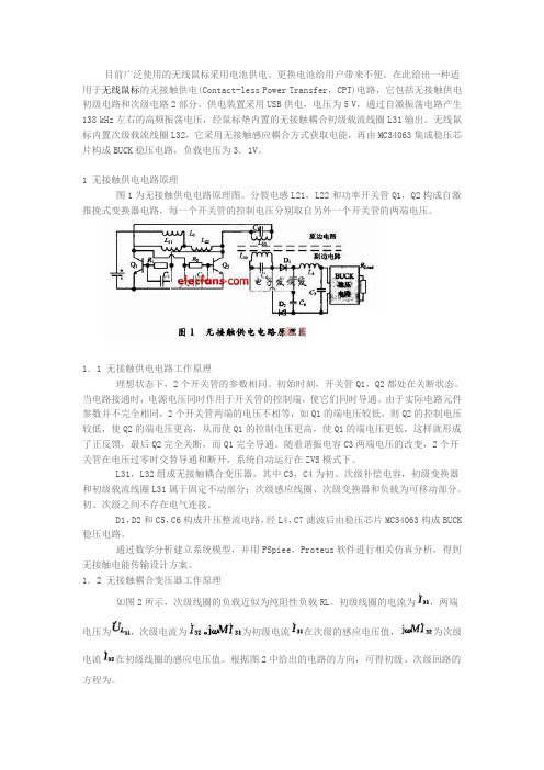
1 无接触供电电路原理图1为无接触供电电路原理图。
分裂电感L21,L22和功率开关管Q1,Q2构成自激推挽式变换器电路,每一个开关管的控制电压分别取自另外一个开关管的两端电压。
1.1 无接触供电电路工作原理理想状态下,2个开关管的参数相同。
初始时刻,开关管Q1,Q2都处在关断状态。
当电路接通时,电源电压同时作用于开关管的控制端,使它们同时导通。
由于实际电路元件参数并不完全相同,2个开关管两端的电压不相等,如Q1的端电压较低,则Q2的控制电压较低,使Q2的端电压更高,从而使Q1的控制电压更高,使Q1的端电压更低,这样就形成了正反馈,最后Q2完全关断,而Q1完全导通。
随着谐振电容C3两端电压的改变,2个开关管在电压过零时交替导通和断开,系统自动运行在ZVS模式下。
L31,L32组成无接触耦合变压器,其中C3,C4为初、次级补偿电容,初级变换器和初级载流线圈L31属于固定不动部分;次级感应线圈、次级变换器和负载为可移动部分。
初、次级之间不存在电气连接。
D1,D2和C5,C6构成升压整流电路,经L4,C7滤波后由稳压芯片MC34063构成BUCK 稳压电路。
通过数学分析建立系统模型,并用PSpiee,Proteus软件进行相关仿真分析,得到无接触电能传输设计方案。
1.2 无接触耦合变压器工作原理如图2所示,次级线圈的负载近似为纯阻性负载RL。
自发电无线鼠标的设计方案及工作原理
第3 0卷 第 4期
2 0 1 4年 7月
森
林
工
程
Vo 1 . 3 0 No . 4
F0RES T ENGI NEERI NG
J u 方 案及 工作 原 理
余 子倩 ,李 洋 ,王 莹 ,张 亮
( 东北林业大学 工程技术学院,哈尔滨 1 5 0 0 4 0 )
t r i c t o a v o i d t h e e x c e s s i v e e n e r g y c o n s u mp t i o n c a u s e d b y e x t e n s i v e u s e o f d r y c e l l a n d s e c o n d a y r p o l l u t i o n o f t h e e n v i r o n me n t p r o b l e m
造 成 环 境 二 次 污染 的 问题 ,有利 于 实现 社 会 可持 续发 展 。
关 键 词 :无 线 鼠 标 ; 自发 电 ;锂 电池
中图 分 类 号 :S 7 7 8
2.4G无线鼠标及RF接收器原理图

---------------------------------------------------------------最新资料推荐------------------------------------------------------2.4G无线鼠标及RF接收器原理图12345678R2 VCC 150K VCCRESTSPI_MISO OSCO C5 OSCI N/A Y1 4MHz RA 1M C2 27P C3 27P主控电路RF电路VCC R5 VCC 150K RF_CS#R6RF_RSTC6 VCC 104R7 4.7~10RTVCCC7 10uF A150KAR1 20KANT U1 P55 P54 TCC GND SPI_MISO SPI_CLK SPI_MOSI RF_CS# LVD# PD#/ID DPI_BTN MBUTTON RBUTTON 1 2 3 4 5 6 7 8 9 10 11 12 13 14 15 16 P55 P54 TCC VDD NC VSS INT P50 P51 P52 P53 P60 P61 P62 P63 P64 P56 P57 RESET OSCI OSCO P77 P76 P75 P74 P73 P72 P71 P70 P67 P66 P65 32 31 30 29 28 27 26 25 24 23 22 21 20 19 18 17 P56 P57 REST OSCI OSCO PKT_FLAG IIC_SDA P75 P74 IIC_SCL SNS_CS# ZWH_C ZWH_A ZWH_B LBUTTON VCC C1 104 C4 104L2 * CF1 *ANT 2. 4GCF2 *VCC+1.8V C16 30PF VCC Y3 12M C15 30PF +1.8V C14 0. 1uF C8 2.2UF ANT R9 680K U3 R8 560R24 23 22 21 20 19C10 0.1uF TVCC C9 0.1uF BSE28A DICE B 1 2 3 4 U2 A0 A1 A2 VSS VCC WP SCL SDA 8 7 6 5 R4 10KXTALO VDD_IN GND CKPHA LDO_VOUT VDD_IOIIC_SCL IIC_SDA24C02(SOP-8)IF_VDD AMS_VDD FIFO_FLAG RXCLK PKT_FLAG GND1 2 3 4 5 6XTALI PLL_VDD VCO_VDD ANT GND RF_VDDSPI_MISO RESET_n SPI_CLK SPI_MOSI SPI_SS DIG_VDD18 17 16 15 14 13SPI_MISO RF_RST SPI_CLK SPI_MOSI RF_CS# +1.8V C11 10nF按键、编码电路S4 DPI_BTN S7 PD#/ID S1 LBUTTON S3 MBUTTON C RBUT TON S2 RIGHT MIDDLE LFETCOM B A7 8 9 10 11 12DPI +1.8V PD/ID1/ 4C13 0.1uF SE1 EC10E8713 DICEC12 10NFPKT_FLAG3 2 1ZWH_C ZWH_B ZWH_ACR3 VCCRST5030#POWER电路B+ BT1 1. 5V X1 C17 104 C18 47uF L1 100uH 3 LXD3 SS12 U4GND低电压检测电路VCC D1 VCC C19 * C20 104 C21 100uF B+ 3 R10 *(150R)GNDSensor电路D2 LED120K R11 VCC *(100R)*R3在16083和A5030上使用, A5090不用R3. *R11在16083和A5030上用100R *R11在A5090上用180RVout2Batt_Low IIC_SCL 1 LVD#U6 SPI_MISO RST5030# SNS_CS# VCC R12 150K ADNS5030 ,16083,A5090 Vout 1 2 3 4 MISO XY_LED NRESET NCS MOSI VDD3 GND SCLK 8 7 6 5 SPI_MOSI VCC GND SPI_CLK VCC + C23 10uF C22 1041BL8530-XX(SOT-89)VinU5 BL8506-XX(SOT-23)D2备注:带*的元器件为选用或根据具体情况选定Title Size A4 Date: File: 1 2 3 4 5 6 Number Revision Sheet of Drawn By: 7DGiGa HiD-V2-SE-5030/16083/509020100309 WYJ8V2.3---------------------------------------------------------------最新资料推荐------------------------------------------------------ 1234AARF电路+1.8V 3V3 C9 0.1uF R3 3.3R RF3V3 C8 0.1uF C7 4.7uF/6.3V主控电路3V3 C2 4.7uF/6.3VD+ 3V3 GND OSCO OSCI+5V C5 4.7uF/10V C1 104OSCOC4 Y1 12M30P(15P)OSCI C3 24P(12P)DSPI_MISO RF_RST#24 23 22 21 20 19OSCI B +1.8V 2.2nF C11 2.2UF ANT L2 ANT1 * CF1 *RFIXP54 P55 P56 P57 P60C141 2 3 4 5D+ V3.3 VSS OSCO OSCI20 19 18 17 16DP92 P93 P52 P53VDD P66 P65 P62 P6115 14 13 12 11+5V LED# E2_WP ID_KEY IIC_SDA BXTALO VDD_IN GND CKPHA LDO_VOUT VDD_IOIF_VDD AMS_VDD FIFO_FLAG RXCLK PKT_FLAG GND1 2 3 4 5 6XTALI PLL_VDD VCO_VDD ANT GND RF_VDDSPI_MISO RESET_n SPI_CLK SPI_MOSI SPI_SS DIG_VDD18 17 16 15 14 13SPI_MISO RF_RST# SPI_CLK SPI_MOSI RF_CS# +1.8V C10 10nF C13 0.1uF R2 3V3 10KSPI_CLK 6 SPI_MOSI 7 8 RF_CS# PKT_FLAG 9 IIC_SCL 10U2 SE95CQ(QFN-20)或SE95CD(DICE)以上是SE95BQ/SE95BD 的升级版1 2 3 SCL GND SDA WP VCC 5 4 E2_WP 3V3 C6 104IIC_SCL GND IIC_SDA+1.8V PKT_FLAG C C12 0.1uF 3V3 R1根据 D1的LED特性确定 R1 0-560R D1 LED LED# +5V DD+ R11 3.3R R9 R10 USBA 33R 33R 1 2 3 4 VCC DD+ GND57 8 9 10 11 12U1 R8713(QFN-24)或8713(DICE)U3 SE24C02TB(TSOT-23-5)CID_KEYL1 SID ID KEY选用电路Bead 需过安规时,R9,R10 ,R11 ,L1用上述值否则直接短路DTitle Size A4 Date: File: 1 2 3GiGa HiD 2.4G Nano RX接收器原理图NumberDGiGa HiD-V2-SE-Nano RXSheet of Drawn By: WYJ3/ 44RevisionV2.320100131。
无线鼠标的设计与实现

无线鼠标的设计与实现摘要:将机械鼠标的滚动动作和左右键的操作转换成开关信号,用方波电路产生的方波信号代替原鼠标内光敏传感器的脉冲信号,用相应的开关动作可以实现鼠标光标移动和鼠标的单双击操作!而用发射和接收电路代替原来的鼠标线,可以实现鼠标的遥控。
设计任务和要求:实现鼠标的长距离(1—50米)遥控。
其中的电路设计包括发射模块(含编码电路)、接收模块(含解码电路)、方波发生电路和开关电路等等电路的设计及它们之间的连接、匹配。
一.无线鼠标电路的设计和实现1.总体方案论证:方案一:在鼠标与电脑接口间用发射和接收电路代替了鼠标线,本方案除了要考虑发射和接收模块外,还要考虑接口协议,如下图。
考虑到时间和难度的问题,没有选择此方案。
方案二:用遥控器控制鼠标,即用遥控器的按键信号控制鼠标的上下左右移动方向和左右键。
只需要考虑发射和接收电路,不需要考虑接口协议,如下图。
选择此方案。
2.发射模块和接收模块的电路的实现方案:方案一:发射模块F05和接受模块J05C的应用。
F05采用声表谐振器稳频,工作频率为315MHZ,以AM方式调制,采用PT2262编码器240mm小拉杆天线发射信号;J05C由超外差电路结构IC芯片和温度补偿电路构成,具有较高的接收灵敏度及稳定性。
芯片内含低噪声射频放大器、混频器、本地振荡器、中频放大器、滤波器及限幅比较器,输出为数据电平信号,直接接至PT2272解码器进行解码,接收天线约22cm。
方案二:利用红外线技术实现红外信号的发射和接收。
发射部分,利用单片机AT89C2051检测坐标位移和按键动作,经过处理按一定的编码输出到发射电路。
接收部分使用红外遥控用专用接收管,如IRM8608S,对红外信号接收和解调,并输出TTL电平;TTL电平的数据流送给单片机进行处理,单片机把该数据转化为符合PS/2鼠标规范的数据报告,发送给计算机。
如图:方案三:利用无线遥控方式实现鼠标的遥控。
原理与上述方案二的原理一样,只是具体的发射和接收电路有所不同。
无线光电鼠标设计
无线光电鼠标设计无线光电鼠标是一种通过光学传感器来感知鼠标在平面上移动并将其转化为电子信号用于控制计算机操作的设备。
相比传统的机械鼠标,光电鼠标具有更高的精确度和灵敏度,且无需使用鼠标垫,操作更为顺畅。
本文将介绍一种基于无线技术的光电鼠标设计。
一、设计原理1.光学传感器:光学传感器是用于感知鼠标在平面上移动的关键组件。
它通过红外线激光照射在平面上,利用接收器接收反射光并转化为电子信号。
光电鼠标通常使用光学传感器,而非机械滚轮来感知鼠标的移动。
2.无线通信:无线光电鼠标采用无线通信技术与计算机进行通信。
一般而言,鼠标通过无线信号传输模块将感测到的鼠标位置信息转化为离散的数字信号,并通过无线接收器发送给计算机。
3.电源管理:由于无线光电鼠标是无线设备,因此电源管理是设计中需要考虑的一个重要因素。
光电鼠标通常通过电池供电,而无线光电鼠标设计中需要考虑如何提高电池寿命,以及如何设计低功耗的电路。
二、无线光电鼠标的设计过程1.系统结构设计:首先,需要设计鼠标的整体结构,包括外壳、按键、光学传感器和无线通信模块等组件的放置。
同时,还需要确定适用于无线光电鼠标的鼠标跟踪算法。
2.硬件设计:硬件设计包括电路设计和电路实现两个阶段。
在电路设计阶段,需要设计电路并选取合适的元器件,如传感器、无线通信模块和按键等。
在电路实现阶段,需要制作电路板及相关电子元件,如红外线激光发射器、激光传感器、无线模块等。
3.软件设计:在软件设计阶段,需要设计鼠标的驱动程序和控制程序。
驱动程序用于控制无线光电鼠标与计算机的通信,而控制程序用于处理鼠标移动数据并将其转化为计算机操作指令,实现指针的移动和点击等功能。
4.电源管理:电源管理是无线光电鼠标设计中的一个关键问题。
设计者需要考虑如何降低系统的功耗以延长电池寿命,例如通过降低工作频率、优化电路中的功耗等方式来实现。
三、设计思路与注意事项1.根据无线光电鼠标的使用场景和目标用户,确定设计要求和性能指标,如无线通信距离、精度和灵敏度等。
无线遥控鼠标电路设计

无线遥控鼠标电路设计一、引言二、功能需求分析1.远程传输鼠标移动信号:用户通过无线遥控器控制鼠标移动,需要将移动信号传输给电脑。
2.按键控制电脑鼠标左右键:用户通过无线遥控器的按键来控制电脑鼠标的左右键操作。
3.光学传感器:鼠标需要具备光学传感器来感知光滑表面,并将移动信号传输给电脑。
三、硬件设计1.遥控器设计a.无线模块:使用无线收发模块,如蓝牙模块或者无线射频模块,来实现与接收端的无线通信。
b.控制电路:设计遥控器的按键电路,将按键信号通过无线模块发送给接收端。
c.电源管理电路:为遥控器提供适当的电源供电,如使用电池或者充电电池。
2.接收端设计a.无线模块:使用与遥控器相匹配的无线收发模块,以接收遥控器发送的信号。
b.微控制器:使用微控制器来处理接收到的信号,进行相应的鼠标操作。
B接口:通过USB接口将处理后的鼠标信号传输给电脑。
d.光学传感器:设计接收端的光学传感器电路,感知鼠标在表面的移动情况,并将移动信号传输给微控制器。
四、软件设计1.遥控器端软件a.编写遥控器端的按键控制软件,将按键操作转换为相应的无线信号。
2.接收端软件a.编写接收端的无线通信软件,接收遥控器发送的信号,并将数据传输给微控制器。
b.编写鼠标操作软件,根据接收到的信号来模拟鼠标的移动和点击操作。
五、测试与优化在完成硬件和软件设计后,需要对整个系统进行测试和优化。
测试时需要验证遥控器的按键操作是否能够正确发送信号并控制鼠标移动和点击,同时需要测试光学传感器的灵敏度和准确性。
对于存在的问题和不足进行优化和改进,确保最终系统的稳定性和性能。
六、总结通过以上的电路设计和软件编写,我们可以实现一个基于无线通信技术的遥控鼠标系统。
该系统能够提供更加便捷的鼠标操作方式,增强用户体验。
在实际应用中,还可以进一步扩展功能,如增加滚轮操作、手势识别等,满足用户不同的需求。
鼠标ic方案

鼠标IC方案概述鼠标是计算机外部设备中最为常见的一种,它通过鼠标指针的移动和按键操作来控制计算机的操作。
鼠标IC(Integrated Circuit)方案是指鼠标硬件设计中的集成电路方案,它负责处理鼠标的信号输入、解码、处理和输出,保证鼠标操作的准确性和稳定性。
本文将介绍鼠标IC方案的基本原理、常见的IC方案及其特点,以及如何选择适合的鼠标IC方案。
基本原理鼠标IC方案的基本原理是通过光学或机械传感器检测鼠标指针在平面上的移动,并将移动信息转换成计算机可以识别的数字信号。
根据传感器的不同,鼠标IC方案可以分为光学鼠标和机械鼠标两种。
光学鼠标光学鼠标使用光电传感器来检测鼠标指针的移动。
光电传感器通常由红外线发射器和红外线接收器组成,发射器发出红外线,当红外线照射到鼠标移动表面上的凹凸不平或颜色变化时,会被接收器接收并产生信号。
鼠标IC会对接收到的信号进行解码和处理,然后输出给计算机。
光学鼠标的优点是精确度高,适用于大多数表面,无需特殊垫子。
而且光学鼠标无机械传动部件,所以耐用性强,使用寿命较长。
机械鼠标机械鼠标使用机械传感器来检测鼠标指针的移动。
机械传感器通常由球体和旋转编码器组成,当鼠标移动时,球体会滚动,旋转编码器会根据球体的滚动方向和速度产生相应的信号。
鼠标IC会对接收到的信号进行解码和处理,然后输出给计算机。
机械鼠标的优点是成本较低、结构简单,适用于一些特殊表面。
然而,机械鼠标需要定期清洁球体和编码器,以保证准确性和稳定性。
并且由于机械传动部件较多,使用寿命相对较短。
常见的IC方案光学鼠标IC方案1.Avago ADNS-3050:Avago ADNS-3050是一种常见的光学鼠标IC方案,具有高精度和低功耗的特点。
它支持多种分辨率和数据输出速率的选择,并且内置了一些增强功能,如自动睡眠模式和运动检测。
这种IC方案适用于各种类型的光学鼠标。
2.PixArt PMW3360:PixArt PMW3360是一种高性能的光学鼠标IC方案,具有极高的分辨率和准确性。
无线射频鼠标设计方案
3D无线射频鼠标的电路设计与实现一种3D无线鼠标设计的新思路,以凌阳单片机为核心控制器,通过MEMS加速度传感器和触控模块。
感知鼠标的移动动作,同时,通过无线射频完成无线通信,从而实现鼠标功能。
使用过程中。
鼠标不仅可以放于载体使用,而且可以在空中使用,增添了鼠标的操控方式,同时,大大增加了此无线鼠标的适用范围。
0引言鼠标作为电脑的一基本部件。
扮演着重要的角色。
随着科技的进步和市场的需求。
鼠标也经历着快速的发展。
传统的鼠标无论是有线鼠标还是无线鼠标。
由于采用控制原理的原因,或者受到线缆的约束,或者离不开对桌面等载体的依赖,适用场合和范围受到限制。
因此,市场上急需一种适用于多种场合。
能满足不同人群特殊功能需求的鼠标,此时。
3D无线鼠标的概念应运而生。
本文通过对运用MEMS加速度传感器。
触控模块和凌阳单片机完成鼠标3D控制原理的阐述。
以及对实验中实际操作的记录为现阶段多功能新型鼠标的制作提供参考依据。
13D无线鼠标的工作原理无线射频鼠标总体分为发射模块(见图1)和接收模块(见图2)两个部分。
发射部分模块集成在手持端,由使用者控制。
接收模块与PC、笔记本等仪器相连。
图1发射模块系统框图图2接收模块系统框图发射模块主要由电阻式触摸屏、MEMS加速度传感器、16位凌阳单片机和nRF2401发射模块组成,主要功能是实现对手势运动趋势信息的采集和发送。
其中触摸屏用于检测使用时坐标X、Y的变化,通过对X、Y变化趋势的分析,完成对鼠标移动轨迹的模拟。
MEMS 加速度传感器则用于感知使用者的动作,通过将这些动作定义为特殊指令。
实现鼠标的特殊功能键。
同时发射模块与接收模块之间通过2.4GHz无线收发一体芯片完成两者之问的无线通信。
最终由接收端的USB驱动电路实现PC端的鼠标控制功能。
其中在通过对X、Y坐标变化,进行算法处理时,需要对操作过程中误差较大的坐标进行滤波,同时简化鼠标的移动方向。
并通过固化匹配的方式,正确反映鼠标的整体的运动趋势。
无线鼠标电路设计及算法实现
无线鼠标电路设计及算法实现周成虎;李小魁;韩大伟【摘要】文中设计的无线鼠标包含发射电路和接收电路两部分,发射电路先采用光传感器ADNS5030检测鼠标的移动信息,然后输出到内置单片机的无线模块CC2430的I/O口,通过CC2430控制并将此信息发射到接收电路,接收电路接收到移动信息后,根据鼠标位移状态机解码算法,得到移动信息及按键信息,通过HT82M98A处理后将信息传给计算机,计算机自动完成相应动作;然后不断的循环;经测试,该电路不仅具备普通有线鼠标的全部功能,还可远距离灵活操纵鼠标,在大礼堂等开阔场所可达80 m以上;计算机自动识别无线鼠标接收电路,不需要额外安装程序,每一次鼠标信号处理总时间不大于1 ms,无线鼠标移动灵活,无停滞现象.%This paper designed wireless mouse contains launch circuit and receiving circuit two parts. The first launch circuit light sensor ADNS5030 detection the mobile information of, mouse and then the output to the built—in wireless module of single chip CC2430 I/O mouth, through the CC2430 control and to this information launch to receiving circuit. Receiving circuit receives mobile information, according to the mouse displacement state machine decoding algorithm, get mobile information and key information, through the HT82M98A treatment will be information on to the computer, the computer automatically complete the corresponding action. Then continuously circulation. By test, this circuit has not only all of the functions of ordinary cable the mouse, and can distance flexible control the mouse, and in the auditorium open place, can reach more than 80 m. Computer automatic identification wireless mousereceiving circuit, do not need extra installation program. Each time the mouse signal processing is no more than the total time 1 ms, wireless mouse flexible, no stagnation phenomenon.【期刊名称】《计算机测量与控制》【年(卷),期】2012(020)012【总页数】3页(P3329-3331)【关键词】无线鼠标;无线模块;无线射频;发射与接收【作者】周成虎;李小魁;韩大伟【作者单位】河南工程学院电气信息工程系,郑州 451191;河南工程学院电气信息工程系,郑州 451191;河南工程学院电气信息工程系,郑州 451191【正文语种】中文【中图分类】TN9230 引言随着计算机技术的发展,有线鼠标的连线给使用者带来许多不便。
2.4G 无线鼠标原理图
ADNB-7051-EV and ADNB-7052-EV Low Power Laser Mouse Bundles Data SheetDescriptionThe Avago Technologies ADNB-7051-EV and ADNB-7052-EV low power laser mouse bundles are the laser-illuminated system enabled for cordless application. Powered by Avago Technologies LaserStream™ technology, the mouse can operate on many surfaces that proved difficult for traditional LED-based optical navigation. Its low power architecture is capable of sens-ing mouse motion while prolonging battery life, two performance areas essential in demanding cordless applications.ADNB-7051-EV and ADNB-7052-EV Low Power Laser Mouse Bundles include: Bundle PartNumber Part Number DescriptionADNB-7051-EV ADNS-7050Low Power Laser Mouse SensorADNV-6340Single-Mode Vertical-Cavity SurfaceEmitting Laser (VCSEL)ADNS-6120Laser Mouse Round LensADNS-6230-001Laser Mouse VCSEL Assembly Clip Bundle PartNumber Part Number DescriptionADNB-7052-EV ADNS-7050Low Power Laser Mouse SensorADNV-6340Single-Mode Vertical-Cavity SurfaceEmitting Laser (VCSEL)ADNS-6130-001Laser Mouse Trim LensADNS-6230-001Laser Mouse VCSEL Assembly Clip The ADNS-7050 sensor along with the ADNS-6120 or ADNS-6130-001 lens, ADNS-6230-001 clip and ADNV-6340 VCSEL form a complete and compact laser mouse tracking system. There is no moving part, which means high reliability and less maintenance for the end user. In addition, precision opti-cal alignment is not required, facilitating high volume assembly.This document will begin with some general information and usage guide-lines on the bundle set, followed by individual detailed information on ADNS-7050 laser mouse sensor, ADNV-6340 VCSEL, ADNS-6120 or ADNS-6130-001 lens and ADNS-6230-001 clip.Overview of Laser Mouse Sensor AssemblyFigure 1. 2D Assembly drawing of ADNB-7052-EV (top and cross-sectional view). 232D Assembly Drawing of ADNB-7051/52-EV, PCBs and Base PlateFigure 2. Exploded view drawing.Shown with ADNS-6130-001 Laser Mouse Lens, ADNS-6230-001 VCSEL As-sembly Clip and ADNV-6340 VCSEL. The components interlock as they are mounted onto defined features on the base plate.The ADNS-7050 laser mouse sensor is designed for mounting on a through hole PCB, looking down. There is an aperture stop and features on the package that align to the lens.The ADNV-6340 VCSEL is recommended for illumination, provides a laser diode with a single longitudinal and a single transverse mode. It is particu-larly suited as lower power consumption and highly coherent replacement of LEDs. It also provides wider operation range while still remaining within single-mode, reliable operating conditions.The ADNS-6120 or ADNS-6130-001 Laser Mouse Lens is designed for use with ADNS-7050 sensor and the illumination subsystem provided by theassembly clip and the VCSEL. Together with the VCSEL, the lens provides the directed illumination and optical imaging necessary for proper operation of the Laser Mouse Sensor. ADNS-6120 and ADNS-6130-001 are precision molded optical components and should be handled with care to avoid scratching of the optical surfaces. ADNS-6120 also has a large round flange to provide a long creepage path for any ESD events that occur at the open-ing of the base plate.The ADNS-6230-001 VCSEL Assembly Clip is designed to provide mechanical coupling of the ADNV-6340 VCSEL to the ADNS-6120 or ADNS-6130-001lens. This coupling is essential to achieve the proper illumination alignment required for the sensor to operate on a wide variety of surfaces.Avago Technologies provides an IGES file drawing describing the base platemolding features for lens and PCB alignment.ADNV-6340 (VCSEL)CUSTOMER SUPPLIED VCSEL PCB* or ADNS-6120 FOR ROUND LENSCUSTOMER SUPPLIED BASE PLATE WITH RECOMMENDED FEATURES PER IGES DRAWING4Figure 3. Recommended PCB mechanical cutouts and spacing.9.Tune the laser output power from the VCSEL to meet the Eye Safe Class I Standard as detailed in the LASER Power Adjustment Procedure.10.Install the mouse top case. There must be a feature in the top case (or other area) to press down onto the sensor to ensure the sensor and lens are interlocked to the correct vertical height.Assembly Recommendation1.Insert the sensor and all other electrical components into the applica-tion PCB (main PCB board and VCSEL PCB board).2.Wave-solder the entire assembly in a no-wash solder process utilizing a solder fixture. The solder fixture is needed to protect the sensor during the solder process. It also sets the correct sensor-to -PCB distance, as the lead shoulders do not normally rest on the PCB surface. The fixture should be designed to expose the sensor leads to solder while shielding the optical aperture from direct solder contact.3.Place the lens onto the base plate.4.Remove the protective kapton tape from the optical aperture of the sensor. Care must be taken to keep contaminants from entering the aperture.5.Insert the PCB assembly over the lens onto the base plate. The sensor aperture ring should self-align to the lens. The optical position refer-ence for the PCB is set by the base plate and lens. Note that the PCB motion due to button presses must be minimized to maintain optical alignment.6.Remove the protective cap from the VCSEL.7.Insert the VCSEL assembly into the lens.8.Slide the clip in place until it latches. This locks the VCSEL and lens together.Design Considerations for Improving ESD PerformanceFor improved electrostatic discharge performance, typical creepage and clearance distance are shown in the table below. Assumption: base plate construction as per the Avago Technologies supplied IGES file and ADNS-6130-001 trim lens (or ADNS-6120 round lens).Typical Distance Millimeters Creepage 12.0Clearance2.1Note that the lens material is polycarbonate and therefore, cyanoacrylate based adhesives or other adhesives that may damage the lens should NOT be used.DIMENSIONS IN MILLIMETERS (INCHES).5Figure 4. Sectional view of PCB assembly highlighting optical mouse components.Figure 5a. Schematic diagram for 3-button scroll wheel corded mouse.EEPROM for Laser Eye Safety for Sun+ ALPC6NotesThe supply and ground paths should be laid out using a star methodology.Level shifting is required to interface a 5V micro-controller to the ADNS-7050. If a 3V micro-controller is used, the 74VHC125 component shown may be omitted.LASER Drive ModeThe laser is driven in pulsed mode during normal operation. A calibration mode is provided which drives the laser in continuous (CW) operation. Eye SafetyThe ADNS-7050 and the associated components in the schematic of Figure 5 are intended to comply with Class 1 Eye Safety Requirements of IEC 60825-1. Avago Technologies suggests that manufacturers perform testing to verify eye safety on each mouse. It is also recommended to review possible single fault mechanisms beyond those described below in the section “Single Fault Detection”. Under normal conditions, the ADNS-7050 generates the drive current for the laser diode (ADNV-6340).In order to stay below the Class 1 power requirements, LASER_CTRL0 (register 0x1a), LASER_CTRL1 (register 0x1f), LSRPWR_CFG0 (register 0x1c) and LSRPWR_CFG1 (register 0x1d) must be programmed to appropriate values. The system comprised of the ADNS-7050 and ADNV-6340, is designed to maintain the output beam power within Class 1 requirements over components manufacturing tolerances and the recommended temperature range when adjusted per the procedure below and imple-mented as shown in the recommended application circuit of Figure 5. For more information, please refer to Eye Safety Application Note AN 5230. LASER Power Adjustment Procedure1.The ambient temperature should be 25°C ±5°C.2.Set VDD to its permanent value.3.Set the Range bit (bit 7 of register 0x1a) to 0.4.Set the Range_C complement bit (bit 7 of register 0x1f) to 1.5.Set the Match_bit (bit 5 of register 0x1a) to the correct value for the bindesignation of the laser being used.6.Set the Match_C_bit (bit 5 of register 0x1f) to the complement of theMatch_bit.7.Enable the Calibration mode by writing to bits [3,2,1] of register 0x1A sothe laser will be driven with 100% duty cycle.8.Write the Calibration mode complement bits to register 0x1f.9.Set the laser current to the minimum value by writing 0x00 to register0x1c, and the complementary value 0xFF to register 0x1d.10.Program registers 0x1c and 0x1d with increasing values to achieve anoutput power as close to 506uW as possible without exceeding it. If this power is obtained, the calibration is complete, skip to step 14.11.If it was not possible to achieve the power target, set the laser current tothe minimum value by writing 0x00 to register 0x1c, and the comple-mentary value 0xff to register 0x1d.12.Set the Range and Range_C bits in registers 0x1a and 0x1f, respectively,to choose to the higher laser current range.13.Program registers 0x1c and 0x1d with increasing values to achieve anoutput power as close to 506uW as possible without exceeding it. 14.Save the value of registers 0x1a, 0x1c, 0x1d, and 0x1f in non-volatilememory in the mouse. These registers must be restored to these values every time the ADNS-7050 is reset.15.Reset the mouse, reload the register values from non-volatile memory,enable Calibration mode, and measure the laser power to verify that the calibration is correct.Good engineering practices such as regular power meter calibration, random quality assurance retest of calibrated mice, etc. should be used to guarantee performance, reliability and safety for the product design.LASER Output PowerThe laser beam output power as measured at the navigation surface plane is specified below. The following conditions apply:1.The system is adjusted according to the above procedure.2.The system is operated within the recommended operating temperaturerange.3.The VDD value is no greater than 300mV above its value at the time ofadjustment.4.No allowance for optical power meter accuracy is assumed.Parameter Symbol Minimum Maximum Units NotesLaser out-LOP716µW Class 1 limit with put power recommendedVCSEL and lens. Disabling the LASERLASER_NEN is connected to the gate of a P-channel MOSFET transistor which when ON connects VDD to the LASER. In normal operation, LASER_NEN is low. In the case of a fault condition (ground or VDD3 at XY_LASER), LASER_NEN goes high to turn the transistor off and disconnect VDD3 from the LASER.Single Fault DetectionADNS-7050 is able to detect a short circuit or fault condition at the XY_LASER pin, which could lead to excessive laser power output. A path to ground on this pin will trigger the fault detection circuit, which will turn off the laser drive current source and set the LASER_NEN output high. When used in combination with external components as shown in the block diagram below, the system will prevent excess laser power for a resistive path to ground at XY_LASER by shutting off the laser. In addition to the ground path fault detection described above, the fault detection circuit is continuously checked for proper operation by internally generating a path to ground with the laser turned off via LASER_NEN. If the XY_LASER pin is shorted to VDD3, this test will fail and will be reported a a fault.7Figure 6. Single fault detection and eye safety feature block diagram.V8ADNS-7050 Laser Mouse Sensor Data SheetTheory of OperationThe ADNS-7050 is based on LaserStream™ Technology, which measures changes in position by optically acquiring sequential surface images (frames) and mathematically determining the direction and magnitude of movement. The ADNS-7050 contains an Image Acquisition System (IAS), a Digital Signal Processor (DSP), and a four wire serial port. The IAS acquires microscopic surface images via the lens and illumination system. These images are pro-cessed by the DSP to determine the direction and distance of motion. The DSP calculates the ∆x and ∆y relative displacement values. An external microcontroller reads the ∆x and ∆y information from the sensor serial port. The microcontroller then translates the data into PS2, USB, or RF signals before sending them to the host PC or game console.Features•Low power architecture•New LaserStream™ technology•Self-adjusting power-saving modes for longest battery life •Speed motion detection up to 20 ips and 8G•Enhanced SmartSpeed self-adjusting frame rate for optimum performance •Motion detect pin output•Internal oscillator – no clock input needed•Selectable 400 and 800 cpi resolution•Wide operating voltage: 2.7 V-3.6 V nominal•Four wire serial port•Minimal number of passive components•Laser fault detect circuitry on-chip for Eye Safety Compliance Applications•Laser mice•Optical trackballs•Integrated input devices•Battery-powered input devicesPinout of ADNS-7050 Optical Mouse SensorPin Name Description1NCS Chip Select (Active Low Input)2MISO Serial Data Output (Master In/Slave Out) 3SCLK Serial Clock Input4MOSI Serial Data Input (Master Out/Slave In) 5MOTION Motion Detect (Active Low Output)6LASER_NEN LASER Enable (Active LOW)7GND Ground8XY_LASER LASER Control9AGND Analog Ground10AVDD Analog Supply Voltage 11AGND Analog Ground12GND Ground13GND Ground14NC No Connection15GND Ground16VDD Supply Voltage17NC No Connection18NC No ConnectionA7050XYYWWZ1 NCS2 MISO3 SCLK4 MOSI5 MOTION6 LASER_NEN7 GND8 XY_LASER9 AGND18 NC17 NC16 VDD15 GND14 NC13 GND12 GND11 AGND10 AVDDFigure 7. Package outline drawing (top view).910Figure 8. Package outline drawing.CAUTION: It is advised that normal static precautions be taken in handling and assembly of this component to prevent damage and/or degradation which may be induced by ESD.NOTES:1. DIMENSIONS IN MILLIMETERS (INCHES).2. DIMENSIONAL TOLERANCE: ± 0.1 mm.3. COPLANARITY OF LEADS: 0.1 mm.4. LEAD PITCH TOLERANCE: ± 0.15 mm.5. CUMULATIVE PITCH TOLERANCE: ± 0.15 mm.6. ANGULAR TOLERANCE: ± 3.0 DEGREES.7. MAXIMUM FLASH: + 0.2 mm.8.CHAMFER (25° X 2) ON THE TAPER SIDE OF THE LEAD.9. * THESE DIMENSIONS ARE FOR REFERENCES ONLY AND SHOULD NOT BE USED TO MECHANICALLY REFERENCE THE SENSOR.PIN 1Figure 9. Block diagram of ADNS-7050 optical mouse sensor.Regulatory Requirements•Passes FCC B and worldwide analogous emission limits when assembled into a mouse with shielded cable and following Avago Technologies recommendations.•Passes IEC-1000-4-3 radiated susceptibility level when assembled into a mouse with shielded cable and following Avago Technologies recom-mendations.•Passes EN61000-4-4/IEC801-4 EFT tests when assembled into a mouse with shielded cable and following Avago Technologies recommendations.•UL flammability level UL94 V-0.•Provides sufficient ESD creepage/clearance distance to avoid discharge up to 15 kV when assembled into a mouse according to usage instruc-tions above.P O W E R A N D C O N T R O LS E R I A L P O R T A N D R E G I S T E R SIMAGE ARRAYDSP OSCILLATORLASER DRIVE GNDAGNDXY_LASER AVDDVDDNCS ADNS-7050SCLK MOSI MISO MOTIONLASER_NENAbsolute Maximum RatingsParameter Symbol Minimum Maximum Units NotesStorage Temperature T S-4085ºCLead Solder Temp260ºC For 10 seconds, 1.6 mm below seating plane. Supply Voltage V DD-0.5 3.7VESD2kV All pins, human body model MIL 883 Method 3015 Input Voltage V IN-0.5V DD + 0.5V All PinsLatchup Current Iout20mA All PinsRecommended Operating ConditionsParameter Symbol Minimum Typical Maximum Units NotesOperating Temperature T A040ºCPower Supply Voltage V DD 2.7 2.8 3.6V Including noisePower Supply Rise Time V RT1µs0 to 2.8 V100msSupply Noise (Sinusoidal)V NA100mVp-p10 kHz - 50 MHzSerial Port Clock Frequency f SCLK1MHz Active drive, 50% duty cycle Distance from Lens Reference Z 2.18 2.40 2.62mm Results in ±0.2 mm minimum DOF. Plane to Surface See Figure 10.Speed S20in/secFigure 10. Distance from lens reference plane to surface, Z.DDParameter Symbol Minimum Typical Maximum Units NotesMotion Delay t MOT-RST23ms From SW_RESET register write to valid motion, assuming after Reset motion is presentShutdown t STDWN50ms From Shutdown mode active to low currentWake from Shutdown t WAKEUP23ms From Shutdown mode inactive to valid motion.Notes: A RESET must be asserted after a shutdown.Refer to section “Notes on Shutdown and Forced Rest”,also note t MOT-RSTForced Rest Enable t REST-EN1s From RESTEN bits set to low currentWake from Forced Rest t REST-DIS1s From RESTEN bits cleared to valid motionMISO Rise Time t r-MISO150300ns C L = 100 pFMISO Fall Time t f-MISO150300ns C L = 100 pFMISO Delay after SCLK t DLY-MISO120ns From SCLK falling edge to MISO data valid, no loadconditionsMISO Hold Time t hold-MISO0.51/f SCLKµs Data held until next falling SCLK edgeMOSI Hold Time t hold-MOSI200ns Amount of time data is valid after SCLK rising edge MOSI Setup Time t setup-MOSI120ns From data valid to SCLK rising edgeSPI Time between t SWW30µs From rising SCLK for last bit of the first data byte, to rising Write Commands SCLK for last bit of the second data byte.SPI Time between Write t SWR20µs From rising SCLK for last bit of the first data byte, to rising and Read Commands SCLK for last bit of the second address byte.SPI Time between Read t SRW500ns From rising SCLK for last bit of the first data byte, to falling and Subsequent t SRR SCLK for the first bit of the address byte of the next Commands command.SPI Read Address-Data t SRAD4µs From rising SCLK for last bit of the address byte, to falling Delay SCLK for first bit of data being read.NCS Inactive after t BEXIT500ns Minimum NCS inactive time after motion burst before next Motion Burst SPI usageNCS to SCLK Active t NCS-SCLK120ns From NCS falling edge to first SCLK rising edgeSCLK to NCS Inactive t SCLK-NCS120ns From last SCLK rising edge to NCS rising edge, for valid MISO (for Read Operation)data transferSCLK to NCS Inactive t SCLK-NCS20µs From last SCLK rising edge to NCS rising edge, for valid MOSI (for Write Operation)data transferNCS to MISO High-Z t NCS-MISO500ns From NCS rising edge to MISO high-Z stateMOTION Rise Time t r-MOTION150300ns C L = 100 pFMOTION Fall Time t f-MOTION150300ns C L = 100 pFTransient Supply Current I DDT45mA Max supply current during a V DD ramp from 0 to 2.8 VDDParameter Symbol Minimum Typical Maximum Units NotesDC Supply Current in I DD_RUN410mA Average current, including LASER current. No load on Various Modes I DD_REST10.5 1.8MISO, MOTION.I DD_REST20.150.4I DD_REST30.050.15Peak Supply Current40mAShutdown Supply Current I DDSTDWN112µA NCS, SCLK = VDDMOSI = GNDMISO = Hi-ZInput Low Voltage V IL0.5V SCLK, MOSI, NCSInput High Voltage V IH V DD – 0.5V SCLK, MOSI, NCSInput Hysteresis V I_HYS100mV SCLK, MOSI, NCSInput Leakage Current I leak±1±10µA Vin = VDD -0.6 V, SCLK, MOSI, NCSXY_LASER Current I LAS0.8mA V xy_laser≥ 0.3 VLP_CFG0 = 0xFFLP_CFG1 = 0x00LASER Current I LAS_FAULT300uA XY_LASER R leakage < 75 kOhms to GND(Fault Mode)Output Low Voltage,V OL0.7V Iout = 1 mA, MISO, MOTIONMISO, LASER_NEN Iout = 1 mA, LASER_NENOutput High Voltage,V OH V DD – 0.7V Iout = -1 mA, MISO, MOTIONMISO, LASER_NEN Iout = -0.5 mA, LASER_NENInput Capacitance C in10pF MOSI, NCS, SCLKTypical Performance CharacteristicsFigure 11. Mean resolution vs. Z at 800 cpi.Figure 12. Average error vs. distance at 800 cpi .Figure 13. Wavelength responsivity.R E L A T I V E R E S P O N S I V I T YWAVELENGTH (nm)Power Management ModesThe ADNS-7050 has three power-saving modes. Each mode has a different motion detection period, affecting response time to mouse motion (Response Time). The sensor automatically changes to the appropriate mode, depending on the time since the last reported motion (Downshift Time). The parameters of each mode are shown in the following table.Mode Response Time (nominal)Downshift Time (nominal)Rest 116.5 ms 237 ms Rest 282 ms 8.4 s Rest 3410 ms504 sMotion Pin TimingThe motion pin is a level-sensitive output that signals the micro-controller when motion has occurred. The motion pin is lowered whenever the motion bit is set; in other words, whenever there is data in the Delta_X or Delta_Y registers. C learing t he m otion b it (by r eading D elta_X a nd D elta_Y, o r w riting to the Motion register) will put the motion pin high.LASER ModeFor power savings, the VCSEL will not be continuously on. ADNS-7050 will flash the VCSEL only when needed.Synchronous Serial PortThe synchronous serial port is used to set and read parameters in the ADNS-7050, and to read out the motion information.The port is a four-wire port. The host micro-controller always initiates com-munication; the ADNS-7050 never initiates data transfers. SCLK, MOSI, and NCS may be driven directly by a micro-controller. The port pins may be shared with other SPI slave devices. When the NCS pin is high, the inputs are ignored and the output is tri-stated.The lines that comprise the SPI port:SCLK:Clock input. It is always generated by the master (the micro-controller).MOSI:Input data. (Master Out/Slave In)MISO:Output data. (Master In/Slave Out)NCS:Chip select input (active low). NCS needs to be low to activate the serial port; otherwise, MISO will be high Z, and MOSI & SCLK will be ignored. NCS can also be used to reset the serial port in case of an error.Chip Select OperationThe serial port is activated after NCS goes low. If NCS is raised during a transaction, the entire transaction is aborted and the serial port will be reset.This is true for all transactions. After a transaction is aborted, the normal address-to-data or transaction-to-transaction delay is still required before beginning the next transaction. To improve communication reliability, all serial transactions should be framed by NCS. In other words, the port should not remain enabled during periods of non-use because ESD and EFT/B events could be interpreted as serial communication and put the chip into an un-known state. In addition, NCS must be raised after each burst-mode transac-tion is complete to terminate burst-mode. The port is not available for further use until burst-mode is terminated.Write OperationWrite operation, defined as data going from the micro-controller to the ADNS-7050, is always initiated by the micro-controller and consists of two bytes. The first byte contains the address (seven bits) and has a “1” as its MSB to indicate data direction. The second byte contains the data. The ADNS-7050 reads MOSI on rising edges of SCLK.Figure14. Write operation.Figure 15. MOSI setup and hold time.11234567891011121314151621D 0D5D 6D 7A 0A 1A 2A 3A 4A 5A 61A 6D 4D 3D 2D 1SCLK NCSMOSIMOSI DRIVEN BY MICRO-CONTROLLERMISOsetup, MOSISCLKMOSIRead OperationA read operation, defined as data going from the ADNS-7050 to the micro-controller, is always initiated by the micro-controller and consists of two bytes. The first byte contains the address, is sent by the micro-controller over MOSI, and has a “0” as its MSB to indicate data direction. The second byte contains the data and is driven by the ADNS-7050 over MISO. The sensor outputs MISO bits on falling edges of SCLK and samples MOSI bits on every rising edge of SCLK.Figure 16. Read operation.Figure 17. MISO delay and hold time.Note: The 0.5/fSCLK minimums high state of SCLK is also the minimum MISO data hold time of the ADNS-7050. Since the falling edge of SCLK is actually the start of the next read or write command, the ADNS-7050 will hold the state of data on MISO until the falling edge of SCLK.Required Timing Between Read and Write CommandsThere are minimum timing requirements between read and write com-mands on the serial port.Figure 18. Timing between two write commands.SCLK NCS SCLK MOSIMISOt WRITE OPERATION WRITE OPERATIONIf the rising edge of the SCLK for the last data bit of the second write command occurs before the required delay (t SWW ), then the first write com-mand may not complete correctly.Figure 19. Timing between write and read commands.If the rising edge of SCLK for the last address bit of the read command occurs before the required delay (t SWR ), the write command may not com-plete correctly.Figure 20. Timing between read and either write or subsequent read commands.During a read operation SCLK should be delayed at least t SRAD after the last address data bit to ensure that the ADNS-7050 has time to prepare the requested data. The falling edge of SCLK for the first address bit of either the read or write command must be at least t SRR or t SRW after the last SCLK rising edge of the last data bit of the previous read operation.Burst Mode OperationBurst mode is a special serial port operation mode that may be used to reduce the serial transaction time for a motion read. The speed improve-ment is achieved by continuous data clocking to or from multiple registers without the need to specify the register address, and by not requiring the normal delay period between data bytes.Burst mode is activated by reading the Motion_Burst register. The ADNS-7050 will respond with the contents of the Motion, Delta_X, Delta_Y, SQUAL,Shutter_Upper, Shutter_Lower, and Maximum_Pixel registers in that or-der. The burst transaction can be terminated anywhere in the sequence after the Delta_X value by bringing the NCS pin high. After sending the register address, the micro-controller must wait t SRAD and then begin read-ing data. All data bits can be read with no delay between bytes by driving SCLK at the normal rate. The data are latched into the output buffer after the last address bit is received. After the burst transmission is complete, the micro-controller must raise the NCS line for at least t BEXIT to terminate burst mode. The serial port is not available for use until it is reset with NCS, even for a second burst transmission.Figure 21. Motion burst timing.WRITE OPERATION NEXT READ OPERATION• • •READ OPERATIONNEXT READor WRITE OPERATION• • •MOTION_BURST REGISTER ADDRESSREAD FIRST BYTEFIRST READ OPERATION READ SECOND BYTE READ THIRD BYTESCLK• • •Notes on Power-upThe ADNS-7050 does not perform an internal power up self-reset; thePOWER_UP_RESET register must be written every time power is applied.The appropriate sequence is as follows:1.Apply power2.Drive NCS high, then low to reset the SPI port3.Write 0x5a to register 0x3a4.Wait for t WAKEUP5.Write 0xFE to register 0x286.Read from registers 0x02, 0x03, and 0x04 (or read these same 3 bytesfrom burst motion register 0x42) one time regardless of the motion pinstate.During power-up there will be a period of time after the power supply ishigh but before any clocks are available. The table below shows the state ofthe various pins during power-up and reset.State of Signal Pins after VDD is ValidPin On Power-Up NCS High before Reset NCS Low before Reset After Reset NCS Functional Hi Low Functional MISO Undefined Undefined Functional Depends on NCS SCLK Ignored Ignored Functional Depends on NCS MOSI Ignored Ignored Functional Depends on NCS XY_LASER Undefined Undefined Undefined Functional MOTION Undefined Undefined Undefined Functional LASER_NEN Undefined Undefined Undefined FunctionalNotes on Shutdown and Forced RestThe ADNS-7050 can be set in Rest mode through the Configuration_Bits register (0x11). This is to allow for further power savings in applications where the sensor does not need to operate all the time.The ADNS-7050 can be set in Shutdown mode by writing 0xe7 to register 0x3b. The SPI port should not be accessed when Shutdown mode is as-serted, except the power-up command (writing 0x5a to register 0x3a). (Other ICs on the same SPI bus can be accessed, as long as the sensor’s NCS pin is not asserted.) The table below shows the state of various pins during shut-down. To deassert Shutdown mode:1. Write 0x5a to register 0x3a.2. Wait for t WAKEUP.3. Write 0xFE to register 0x28.4. Any register settings must then be reloaded.Pin Status when Shutdown ModeNCS Functional*1MISO Undefined*2SCLK Ignore if NCS = 1*3MOSI Ignore if NCS = 1*4XYLASER High(Off)LASER_NEN High(Off)MOTION Undefined *2*1 NCS pin must be held to 1 (high) if SPI bus is shared with other devices. It is recommended to hold to 1 (high) during Power Down unless powering up the Sensor. It must be held to 0 (low) if the sensor is to be re-powered up from shutdown (writing 0x5a to register 0x3a).*2 Depend on last state.*3 SCLK is ignore if NCS is 1 (high). It is functional if NCS is 0 (low).*4 MOSI is ignore if NCS is 1 (high). If NCS is 0 (low), any command present on the MOSI pin will be ignored except power-up command (writing 0x5a to register 0x3a).Note: There are long wakeup times from shutdown and forced Rest. These features should not be used for power management during normal mouse motion.。
无线键盘、鼠标工作原理
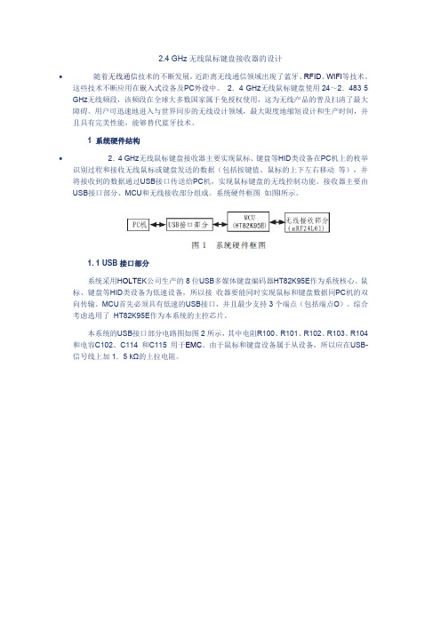
2.4 GHz无线鼠标键盘接收器的设计∙随着无线通信技术的不断发展,近距离无线通信领域出现了蓝牙、RFID、WIFI等技术。
这些技术不断应用在嵌入式设备及PC外设中。
2.4 GHz无线鼠标键盘使用24~2.483 5 GHz无线频段,该频段在全球大多数国家属于免授权使用,这为无线产品的普及扫清了最大障碍。
用户可迅速地进入与世界同步的无线设计领域,最大限度地缩短设计和生产时间,并且具有完美性能,能够替代蓝牙技术。
1 系统硬件结构∙2.4 GHz无线鼠标键盘接收器主要实现鼠标、键盘等HID类设备在PC机上的枚举识别过程和接收无线鼠标或键盘发送的数据(包括按键值、鼠标的上下左右移动等),并将接收到的数据通过USB接口传送给PC机,实现鼠标键盘的无线控制功能。
接收器主要由USB接口部分、MCU和无线接收部分组成。
系统硬件框图如图l所示。
1. 1 USB接口部分系统采用H OLT EK公司生产的8位USB多媒体键盘编码器HT82K95E作为系统核心。
鼠标、键盘等HID类设备为低速设备,所以接收器要能同时实现鼠标和键盘数据同PC机的双向传输。
MCU首先必须具有低速的USB接口,并且最少支持3个端点(包括端点O)。
综合考虑选用了 HT82K95E作为本系统的主控芯片。
本系统的USB接口部分电路图如图2所示,其中电阻R100、R101、R102、R103、R104和电容C102、C114和C115用于EMC。
由于鼠标和键盘设备属于从设备,所以应在USB-信号线上加1.5 kΩ的上拉电阻。
1.2 MCU部分MCU的复位电路采用由R108和C105组成的RC积分电路实现上电复位功能。
上电瞬间,由于电容电压不能突变,所以复位引脚为低电平,然后电容开始缓慢充电,复位引脚电位开始升高,最后变为高电平,完成芯片的上电复位。
HT82K95E微控制器内部还包含一个低电压复位电路(LVR),用于监视设备的供电电压。
如果设备的供电电压下降到0.9 V~VLVR的范围内并且超过1 ms的时间,那么LVR就会自动复位设备。
无线鼠标原理图

几种鼠标电路图1、USB接口鼠标电路图2、电脑无线鼠标电路图3、光电鼠标电路图4、鼠标电路图5、有线USB 光学游戏鼠标电路图A5020方案6、有线USB激光鼠标电路图7、3键USB 有线激光游戏鼠标电路图A7550+CY63743方案8、自制无线鼠标电路图光电鼠标电路图1、两款光电鼠标电路光电鼠标电路一般由两片集成电路与外围元件组成。
一片稍大的是COMS 感光集成电路,另一片一般为鼠标专用集成电路。
CMOS 感光芯片通过检测光电部件因鼠标移动产生的光线变化而得到位置信号,送到鼠标专用集成电路的X、Y 输入端。
而鼠标专用集成电路再检测左、右按键,滚轮键及滚轮前后转到等信息随着CLK时钟信号一起传输给计算机的PS2 或USB 端口。
USB 光电鼠标电路图①为使用GL603 - USB 鼠标集成电路芯片和H2000(400CPI、每秒1500 次扫描) 光电感应芯片的USB 光电鼠标电路图。
PS2 接口鼠标电路图②为使用PAN101 - 208 (800CPI 光学分辨率,2000 次扫描/ 秒) 光电感应芯片和84510 系列鼠标集成电路芯片的PS2 接口光电鼠标电路。
2、光电鼠标原理与电路图传统光学鼠标的工作原理传统光学鼠标工作原理示意图光学跟踪引擎部分横界面示意图光学鼠标主要由四部分的核心组件构成,分别是发光二极管、透镜组件、光学引擎(Optical Engine)以及控制芯片组成。
光学鼠标通过底部的LED灯,灯光以30度角射向桌面,照射出粗糙的表面所产生的阴影,然后再通过平面的折射透过另外一块透镜反馈到传感器上。
当鼠标移动的时候,成像传感器录得连续的图案,然后通过“数字信号处理器”(DSP)对每张图片的前后对比分析处理,以判断鼠标移动的方向以及位移,从而得出鼠标x, y方向的移动数值。
再通过SPI 传给鼠标的微型控制单元(Micro Controller Unit)。
鼠标的处理器对这些数值处理之后,传给电脑主机。
无线鼠标原理图
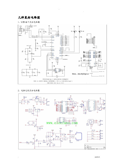
几种鼠标电路图1、USB接口鼠标电路图2、电脑无线鼠标电路图3、光电鼠标电路图4、鼠标电路图5、有线USB 光学游戏鼠标电路图A5020方案6、有线USB激光鼠标电路图7、3键USB 有线激光游戏鼠标电路图A7550+CY63743方案8、自制无线鼠标电路图光电鼠标电路图1、两款光电鼠标电路光电鼠标电路一般由两片集成电路与外围元件组成。
一片稍大的是COMS 感光集成电路,另一片一般为鼠标专用集成电路。
CMOS 感光芯片通过检测光电部件因鼠标移动产生的光线变化而得到位置信号,送到鼠标专用集成电路的X、Y 输入端。
而鼠标专用集成电路再检测左、右按键,滚轮键及滚轮前后转到等信息随着CLK时钟信号一起传输给计算机的PS2 或USB 端口。
USB 光电鼠标电路图①为使用GL603 - USB 鼠标集成电路芯片和H2000(400CPI、每秒1500 次扫描) 光电感应芯片的USB 光电鼠标电路图。
PS2 接口鼠标电路图②为使用PAN101 - 208 (800CPI 光学分辨率,2000 次扫描/ 秒) 光电感应芯片和84510 系列鼠标集成电路芯片的PS2 接口光电鼠标电路。
2、光电鼠标原理与电路图传统光学鼠标的工作原理传统光学鼠标工作原理示意图光学跟踪引擎局部横界面示意图光学鼠标主要由四局部的核心组件构成,分别是发光二极管、透镜组件、光学引擎〔Optical Engine〕以及控制芯片组成。
光学鼠标通过底部的LED灯,灯光以30度角射向桌面,照射出粗糙的外表所产生的阴影,然后再通过平面的折射透过另外一块透镜反应到传感器上。
当鼠标移动的时候,成像传感器录得连续的图案,然后通过“数字信号处理器〞(DSP)对每张图片的前后比照分析处理,以判断鼠标移动的方向以及位移,从而得出鼠标x, y方向的移动数值。
再通过SPI传给鼠标的微型控制单元〔Micro Controller Unit〕。
鼠标的处理器对这些数值处理之后,传给电脑主机。
浅析电子产品无线鼠标的设计与实现

浅析电子产品无线鼠标的设计与实现电子产品无线鼠标是现代人们在使用电脑时常用的一种外设产品,它在使用过程中不受线缆束缚,具有方便携带、操作灵活、使用舒适等优点。
但要实现无线鼠标这一功能,需要设计和实现一系列技术方案,以确保产品的性能稳定、使用安全和便捷。
本文将从电子产品无线鼠标的设计原理、技术方案、实现步骤等方面进行浅析。
一、设计原理在设计无线鼠标时,需要考虑到其通信原理、电源供应、传感器技术等方面的问题。
在通信原理方面,通常采用无线射频技术来实现鼠标与电脑之间的通信。
这种技术能够保证鼠标与电脑之间的稳定连接,同时又能够避免干扰其他无线设备的信号,确保通信质量。
在电源供应方面,一般会采用电池供电或者采用充电电池的方式来为无线鼠标提供电力。
这样可以保证鼠标在使用过程中不会出现断电的情况,保证用户的使用体验。
在传感器技术方面,一般采用光学传感器或者激光传感器来实现鼠标的光标追踪。
这种传感器技术可以保证鼠标在不同表面上都能够稳定的工作,满足用户的不同需求。
二、技术方案在设计无线鼠标的技术方案时,需要考虑到其硬件设计和软件设计两个方面。
在硬件设计方面,一般需要考虑到电路设计、无线通信模块、电源管理、传感器技术等问题。
在电路设计方面,需要保证电路稳定可靠,能够满足鼠标工作的需求。
在无线通信模块方面,需要选择合适的通信模块,保证鼠标与电脑之间的无线通信稳定可靠。
在电源管理方面,需要设计合理的电池供电或者充电电池管理方案,保证鼠标在使用过程中不会出现断电的情况。
在传感器技术方面,需要选择合适的传感器技术,保证鼠标在不同表面上都能够稳定的工作。
在软件设计方面,一般需要考虑到通信协议、鼠标驱动、无线连接管理等问题。
在通信协议方面,需要制定合适的通信协议,保证鼠标与电脑之间的通信稳定可靠。
在鼠标驱动方面,需要设计合理的驱动程序,保证鼠标在不同系统上都能够正常工作。
在无线连接管理方面,需要设计合理的连接管理程序,保证鼠标与电脑之间的无线连接稳定可靠。
无线光电鼠标设计
无线光电鼠标设计李群林电气与信息工程学院测试计量技术与仪器,湖南大学,湖南长沙,410082摘要:无线鼠标技术已相当成熟,市面上已有大量无线鼠标上市,但是价格悬殊很大,本文从无线光电鼠标原理出发,探讨如何设计不同档次的无线光电鼠标。
关键字:USB,无线鼠标,光电鼠标,鼠标1.技术可行性研究无线鼠标技术已相当成熟,市面上已有大量无线鼠标上市,价格在100到600元之间。
有红外和无线电等传输方式;接口类型是USB和PS2;大部分是光电鼠标,也有部分低价的滚轮鼠标,但是由于滚轮鼠标易受灰尘影响,大部分场合工作都不是很理想,故本文只讨论光电鼠标。
2.光电鼠标原理光电鼠标的光学传感器象一部DC/DV一样,跟随操作者的移动连续记录它途经表面的“快照”(假想一下间谍卫星拍摄地球表面的情形,不过比喻不是很恰当,比如光电鼠标是自带光源的,并且它的移动是没有规律的等等),这些快照(即帧)是有一定的频率(即扫描频率、刷新率、帧速率等,以下我们对此不加区分)和尺寸及分辨率(即光学传感器的CMOS晶振的有效像素数),并且光学传感器的透镜应具备一定的放大作用;而光电鼠标的核心――DSP通过对比这些快照之间的差异从而识别移动的方向和位移量,并将这些确定的信息加以封装后通过USB接口源源不断地进入PC;驱动程序(可以是Windows 的默认驱动)则根据这些信号经过一定的转换(参照关系由驱动设置)最终决定鼠标指针在屏幕上的位置。
由此,我们可知一个大略的“(鼠标移动)表面->镜头(组)->光学传感器CMOS 晶阵->DSP->USB接口->驱动程序->PC屏幕坐标”的过程了。
光电鼠标的两个重要参数:光学分辨率和扫描频率。
目前市场上光电鼠标的光学分辨率多数为400DPI和800DPI两种,其含义就是鼠标每移动2.54厘米的距离,光标在屏幕上移动的距离就是400像素和800像素。
扫描频率主要是指光学扫描芯片每秒钟所获得的快照的数量。
基于微机电系统的无线鼠标方案
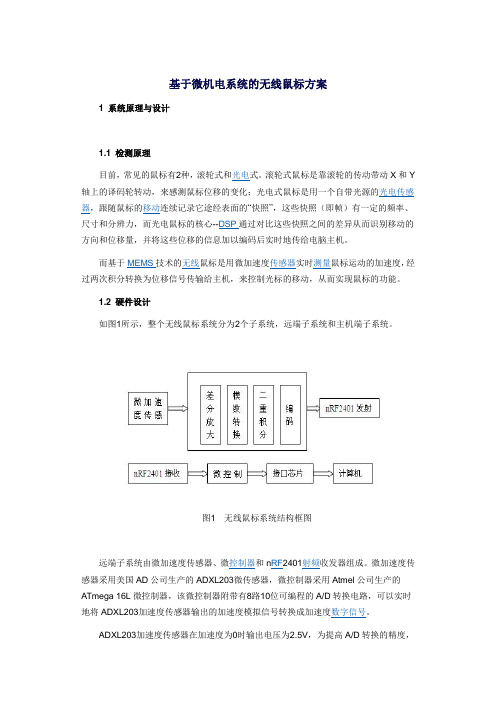
基于微机电系统的无线鼠标方案1 系统原理与设计1.1 检测原理目前,常见的鼠标有2种,滚轮式和光电式。
滚轮式鼠标是靠滚轮的传动带动X和Y 轴上的译码轮转动,来感测鼠标位移的变化;光电式鼠标是用一个自带光源的光电传感器,跟随鼠标的移动连续记录它途经表面的“快照”,这些快照(即帧)有一定的频率、尺寸和分辨力,而光电鼠标的核心--DSP通过对比这些快照之间的差异从而识别移动的方向和位移量,并将这些位移的信息加以编码后实时地传给电脑主机。
而基于MEMS技术的无线鼠标是用微加速度传感器实时测量鼠标运动的加速度,经过两次积分转换为位移信号传输给主机,来控制光标的移动,从而实现鼠标的功能。
1.2 硬件设计如图1所示,整个无线鼠标系统分为2个子系统,远端子系统和主机端子系统。
图1无线鼠标系统结构框图远端子系统由微加速度传感器、微控制器和n RF2401射频收发器组成。
微加速度传感器采用美国AD公司生产的ADXL203微传感器,微控制器采用Atmel公司生产的ATmega 16L微控制器,该微控制器附带有8路10位可编程的A/D转换电路,可以实时地将ADXL203加速度传感器输出的加速度模拟信号转换成加速度数字信号。
ADXL203加速度传感器在加速度为0时输出电压为2.5V,为提高A/D转换的精度,本文利用ATmega 16L内置的差分放大功能,用差分信号将这2.5V电压给滤掉,并将差分后的电压信号放大到与A/D转换的参考电压相匹配。
系统供电采用电器中常见的9V电池,连接一个LM78M05稳压贴片得到恒定的5V电压,供各个模块使用。
主机端子系统由nRF2401射频收发器,串行传输接口芯片和另一个ATmega 16L微控制器组成,其中,RS232串行通信接口芯片采用的是Maxim2IC公司的MAX233芯片,作用是将微控制器输出的5V TTL/CMOS电平转换为EIA/TIA-232-E电平,以便与电脑主机进行串行(RS232)通信。
介绍无线鼠标电路图
介绍无线鼠标电路图<<版权声明:本文由容源电子网(www_dziuu_com)整理提供,部分内容来源于网络,如有侵犯到你的权利请与我们联系更正。
》该装置编译码电路MC145026/MC145027和射频发射/接收模块TDA1808/TDA1809互相配合,可以在10~120m范围内灵活操纵鼠标,而且制作时无须对原有鼠标的外观及内部电路做改动,使用起来符合操作习惯,方便可靠,非常适合爱好者自制。
<<版权声明:本文由容源电子网(www_dziuu_com)整理提供,部分内容来源于网络,如有侵犯到你的权利请与我们联系更正。
》下,鼠标与电脑的连接线内部有4根电路连接线(该电路装置最多可以接受4条数据线输入,读者可根据自己鼠标的选择)分别是电源正极、电源地、数据线1、数据线2。
<<版权声明:本文由容源电子网(www_dziuu_com)整理提供,部分内容来源于网络,如有侵犯到你的权利请与我们联系更正。
》我们将鼠标连线割断,分别找出这4根线,MC145026编码电路的数据传送端D6和D7接受鼠标数据线1和数据线2传来的数据,并在芯片内部编码后经射频发射模块TDA1808发射出去。
<<版权声明:本文由容源电子网(www_dziuu_com)整理提供,部分内容来源于网络,如有侵犯到你的权利请与我们联系更正。
》射频发射模块TDA1809工作后,将接收到的编码信息输入MC145027译码电路,经其转换后在该芯片数据输出端D6和D7复原原鼠标数据线1和数据线2的信号,并通过原鼠标与电脑的连接线送入计算机。
可以看出,上述电路无须改动鼠标及计算机,无须安装额外的鼠标驱动软件,原有鼠标的功能亦能正常使用。
<<版权声明:本文由容源电子网(www_dziuu_com)整理提供,部分内容来源于网络,如有侵犯到你的权利请与我们联系更正。
- 1、下载文档前请自行甄别文档内容的完整性,平台不提供额外的编辑、内容补充、找答案等附加服务。
- 2、"仅部分预览"的文档,不可在线预览部分如存在完整性等问题,可反馈申请退款(可完整预览的文档不适用该条件!)。
- 3、如文档侵犯您的权益,请联系客服反馈,我们会尽快为您处理(人工客服工作时间:9:00-18:30)。
无线鼠标系统电路设计方案大全(三款电路设计原理
详细)
无线鼠标系统电路设计方案(一)
设计的无线鼠标,以CC2430为控制芯片构成发射电路和接收电路。
发射电路负责采集与发送鼠标按键的移动信息,接收电路负责信息接收、处理并与计算机通信。
1、发射部分的电路设计
发射部分的硬件电路由鼠标移动光学传感器ADNS5030、鼠标按键、无线发射模块CC2430(软件设置为发送模式)构成。
由光学传感器ADNS5030检测鼠标的移动信息,将采集到的信息经过SPI 串行接口传递给CC2430处理并发送出去。
发射部分的电路图见图
2。
ADNS-5030光学传感器,功耗低且尺寸小,能高速检测鼠标运动。
它包含图像采集系统(IAS)、数字信号处理器(DSP)和串行总线端口。
IAS将采集的图像通过数字信号处理,计算鼠标在dx和dy方向的相对位移值,决定移动的方向及距离。