STM32_7816智能卡接口笔记
7816物理及协议部分知识整理

工 程 技 术 文 件题目:7816物理及协议部分知识整理摘要:本文档是针对PBOC 银行卡检测需求对7816物理电气特性和协议传输等相关知识的整合。
归 档 类 签 名 项相 关 项相关人日 期 相 关 项签 名日 期 接 收拟 制 魏晓伟 10年3月3日归 档 课题组长魏晓伟打 字 魏晓伟 登记号校 核 魏晓伟位置/ID 号 WISDOM42 MR 号审 核保管期限 长 期 分类号总 工 刘大力关 键 词当前路径 \\Nt02\fangzhen\IDCARD\设计二部与曹总交互目录\100302_7816物理相关文档\7816物理及协议部分知识整理.doc归档路径工程归类北京多思科技工业园股份有限公司公司机密 第 一 稿 共 9 页7816物理及协议部分知识整理1.物理特性 (4)1.1IC卡的一般特性 (4)1.2变形特性 (4)1.3可燃性 (4)1.4有毒性 (4)1.5耐化学性 (4)1.6温度稳定性 (4)1.7湿度 (4)1.8光 (4)1.9带凸印卡 (4)1.10带有磁条的卡 (4)1.11卡的材料 (4)1.12ID-1型卡的翘曲 (5)1.13表面畸变 (5)1.14污染 (5)1.15紫外线 (5)1.16X—射线 (5)1.17触点的表面断面 (5)1.18机械强度(卡和触点) (5)1.19(触点的)电阻 (5)1.20静电 (6)1.21散热 (6)2附加信息记录的方法 (6)2.1凸印(当IC卡带有凸印时) (6)2.2磁条(当IC卡带有磁条时) (6)3IC卡的尺寸和触点位置 (6)3.1IC卡的尺寸 (6)3.2触点尺寸和位置 (6)4电气特性 (8)4.1总则 (8)4.1.1电路 (8)4.2操作条件 (8)4.2.1操作条件的类别 (8)4.2.2操作类别的选择 (8)4.3电压和电流值 (10)4.3.1测量规定 (10)4.3.2VCC (10)4.3.3I/O (10)4.3.4CLK (11)4.3.5RST (11)4.3.6VPP (12)4.3.7外特性 (13)4.3.8卡操作过程 (16)5ATR容量 (18)6字符间隔测试 (19)6.1T=0 (19)6.2T=1 (19)1.物理特性1.1IC卡的一般特性ISO 7810中规定的各类识别卡的物理特性适用于IC卡,ISO 7813中描述的金融交易卡的全部尺寸要求也应适用于这类卡。
STM32笔记(六)
STM32笔记(六)SD卡的读写和FatFS文件系统因为要用,学习了一下SPI操作SD卡,同时移植了一个免费开源的FAT 文件系统:FatFS。
感觉挺好,在单片机上实现了读写文件的操作,接下来就可以解释我的G代码咯!我的SD卡底层操作参考了网上几种常见的代码,但又对其结构做了一定的优化,至少看起来用起来比较方便。
既可以作为文件系统的diskio使用,也可以直接使用底层函数,把SD卡作为一块flash读写。
FatFs文件系统体积蛮小,6-7K足矣,对于128Kflash的STM32来说很合适,代价不大。
同时可移植性很高,最少只需要4个函数修改既可以实现文件系统的移植。
相关文件系统的介绍请看这里。
这里给一套比较完整的参考资料,包括fatfs文件系统的原版资料、几个重要的手册和网上下载的代码。
/bbs/bbs_content.jsp?bbs_sn=3210864&bbs_page_no =1&bbs_id=3020下面是我的代码:其中底层的SPI总线对SD卡的操作在SPI_SD_driver.c/h中,而FATFS 的移植文件diskio.c中对磁盘的操作函数中将调用底层的操作函数。
下面是一些底层操作函数:u8 SPI_ReadWriteByte(u8 TxData); //SPI总线读写一个字节u8 SD_WaitReady(void); //等待SD卡就绪u8 SD_SendCommand(u8 cmd, u32 arg, u8 crc); //SD卡发送一个命令u8 SD_SendCommand_NoDeassert(u8 cmd, u32 arg, u8 crc); //SD卡发送一个命令,不断线u8 SD_Init(void); //SD卡初始化u8 SD_ReceiveData(u8 *data, u16 len, u8 release); //SD卡读数据u8 SD_GetCID(u8 *cid_data); //读SD卡CID u8 SD_GetCSD(u8 *csd_data); //读SD卡CSD u32 SD_GetCapacity(void); //取SD卡容量u8 SD_ReadSingleBlock(u32 sector, u8 *buffer); //读一个sect oru8 SD_WriteSingleBlock(u32 sector, const u8 *buffer); //写一个sect oru8 SD_ReadMultiBlock(u32 sector, u8 *buffer, u8 count); //读多个sect oru8 SD_WriteMultiBlock(u32 sector, const u8 *data, u8 count); //写多个se ctor这是diskio.c中的一段代码,在disk初始化中,我们调用了SPI_SD_drive r.c中的SD卡初始化函数。
STM32学习笔记2

1.通信:设备间信息的交互有线:以太网,USART,USB,CAN,485等无线:wifi,蓝牙,zigbee,射频,红外,2.4G,2G、3G、4G、5G,NB_IOT,广播等2.通信方式划分并行通信:一次传输多位数据,传输速度快,MCU与内存间串行通信:一次传输一位数据串行通信按照数据传输是否同步分为:同步通信:数据传送是以数据块(一组字符)为单位,字符与字符之间、字符内部的位与位之间都同步,需要有同步时钟。
异步通信:字符与字符间的传送是完全异步的,位与位之间的传送基本上是同步的。
串行通信按照数据传输方向划分:单工:数据单向传输-- 广播,收音机等半双工:数据可以双向传输,同一时刻,只能发送或者接收-- 对讲机,485等全双工:数据双向传输-- 手机,SPI等3.串行通信1.物理层1.引脚TXD 数据发送管脚RXD 数据接收管脚GND 信号地2.连接方式a.直接相连-- 模块与模块间,设备与模块间b.RS232 负逻辑电平 1 -- -3~-15V 0 -- +3~+15V-- 设备与设备间,设备与模块间B转串口-- 设备与设备间2.数据链路层(协议)-- 位协议RS232协议:起始位数据位奇偶检验位停止位位数: 1 8/9 1 1~2电平:0 1/0 1/0 1奇偶检验:数据位1的个数+校验位中1的个数奇校验:数据位1的个数+校验位中1的个数为奇数个。
发送的数据:0110 1001发送数据:0110 1001 1接收数据:0110 0001 1 -- 错误0111 0001 1 -- 正确(错误)位:clk周期常用的格式:1+8+0+13.波特率数据传输的速率,每秒传输多少位数据。
常用的波特率:9600,115200,38400等4.STM32中串口的介绍1.数量-- 3个2.特性全双工异步通信小数波特率发生器系统数据字长度可编程(8 位或9 位)停止位可配置- 支持 1 或 2 个停止位发送器和接收器具有单独使能位传输检测标志:—接收缓冲区已满—发送缓冲区为空—传输结束标志3.结构框图1.数据发送和接收数据接收:data = USARTx->DR;数据发送:USARTx->DR = data;2.发送接收控制 -- CR1,CR2,CR33.发送和接收什么时候完成 -- SRTXE:数据发送完成,TDR无数据,移位寄存器有数据TC:数据发送完成,TDR无数据,移位寄存器无数据RXNE:0 –未接收数据 1 - 接收到数据4.波特率5.软件编程1.查看原理图PA9、PA10 复用功能6.蓝牙CC2541工作模式:1.命令响应模式-- 使用AT指令集2.透传模式(透明传输)-- 使用串口发送消息PA6 –通用推挽输出中断配置:优先级4位:占先优先级+ 次级优先级(数字越小,优先级越高)占先优先级:中断发生时能否被打断,谁先执行次级优先级:占先优先级相同时,中断同时到来,优先级高的先执行作业:APP 发送数据*12# ,电机转动发送数据*34# ,电机停止转动。
stm32智能卡函数库
AN2646Application note Smartcard interface with the STM8S microcontrollerIntroductionThis document describes a firmware and hardware smartcard interface solution based onthe STM8 UART1 peripheral. The main purpose of this firmware and hardware package is toprovide resources that facilitate the development of an application using the UART1peripheral in smartcard mode.The firmware interface consists of library source files developed so as to support theISO7816-3/4 specification. An application example is also provided.This document and its associated firmware are available for download from theSTMicroelectronics website: .August 2008 Rev 21/43Contents AN2646 - Application noteContents1Smartcard interface description . . . . . . . . . . . . . . . . . . . . . . . . . . . . . . . 41.1Introduction . . . . . . . . . . . . . . . . . . . . . . . . . . . . . . . . . . . . . . . . . . . . . . . . 41.2External interface . . . . . . . . . . . . . . . . . . . . . . . . . . . . . . . . . . . . . . . . . . . . 41.3Protocol . . . . . . . . . . . . . . . . . . . . . . . . . . . . . . . . . . . . . . . . . . . . . . . . . . . 41.4Smartcard clock generator . . . . . . . . . . . . . . . . . . . . . . . . . . . . . . . . . . . . . 5 2Smartcard reader hardware connection . . . . . . . . . . . . . . . . . . . . . . . . . 63ISO7816 – protocol overview . . . . . . . . . . . . . . . . . . . . . . . . . . . . . . . . . 83.1Introduction . . . . . . . . . . . . . . . . . . . . . . . . . . . . . . . . . . . . . . . . . . . . . . . . 83.2ISO 7816-2 – pin location . . . . . . . . . . . . . . . . . . . . . . . . . . . . . . . . . . . . . . 84ISO 7816-3 – electronic signal and transmission protocol . . . . . . . . . 104.1Card power-up and reset . . . . . . . . . . . . . . . . . . . . . . . . . . . . . . . . . . . . . 114.2Data transfer . . . . . . . . . . . . . . . . . . . . . . . . . . . . . . . . . . . . . . . . . . . . . . . 124.3Answer to reset (A TR) . . . . . . . . . . . . . . . . . . . . . . . . . . . . . . . . . . . . . . . 165ISO 7816-4 – smartcard commands . . . . . . . . . . . . . . . . . . . . . . . . . . . . 185.1T0 protocol . . . . . . . . . . . . . . . . . . . . . . . . . . . . . . . . . . . . . . . . . . . . . . . . 185.2Application-level protocols . . . . . . . . . . . . . . . . . . . . . . . . . . . . . . . . . . . . 205.2.1The ISO 7816-4 APDU . . . . . . . . . . . . . . . . . . . . . . . . . . . . . . . . . . . . . 215.2.2File system API . . . . . . . . . . . . . . . . . . . . . . . . . . . . . . . . . . . . . . . . . . . 225.2.3ISO 7816-4 functions . . . . . . . . . . . . . . . . . . . . . . . . . . . . . . . . . . . . . . . 235.2.4Security API . . . . . . . . . . . . . . . . . . . . . . . . . . . . . . . . . . . . . . . . . . . . . . 246Smartcard interface library: description . . . . . . . . . . . . . . . . . . . . . . . . 266.1File organization . . . . . . . . . . . . . . . . . . . . . . . . . . . . . . . . . . . . . . . . . . . . 266.2Smartcard interface library functions . . . . . . . . . . . . . . . . . . . . . . . . . . . . 266.2.1SC_Handler function . . . . . . . . . . . . . . . . . . . . . . . . . . . . . . . . . . . . . . . 276.2.2SC_PowerCmd . . . . . . . . . . . . . . . . . . . . . . . . . . . . . . . . . . . . . . . . . . . 306.2.3SC_Reset . . . . . . . . . . . . . . . . . . . . . . . . . . . . . . . . . . . . . . . . . . . . . . . 306.2.4SC_ParityErrorHandler . . . . . . . . . . . . . . . . . . . . . . . . . . . . . . . . . . . . . 316.2.5SC_PTSConfig . . . . . . . . . . . . . . . . . . . . . . . . . . . . . . . . . . . . . . . . . . . 31 2/43AN2646 - Application note Contents6.3How to send APDU commands to the smartcard . . . . . . . . . . . . . . . . . . . 326.3.1SC_GET_A2R . . . . . . . . . . . . . . . . . . . . . . . . . . . . . . . . . . . . . . . . . . . . 326.3.2SELECT_FILE . . . . . . . . . . . . . . . . . . . . . . . . . . . . . . . . . . . . . . . . . . . . 326.3.3SC_GET_RESPONSE . . . . . . . . . . . . . . . . . . . . . . . . . . . . . . . . . . . . . 326.3.4SC_READ_BINARY . . . . . . . . . . . . . . . . . . . . . . . . . . . . . . . . . . . . . . . . 336.3.5SC_CREATE_FILE . . . . . . . . . . . . . . . . . . . . . . . . . . . . . . . . . . . . . . . . 336.3.6SC_UPDATE_BINARY . . . . . . . . . . . . . . . . . . . . . . . . . . . . . . . . . . . . . . 346.3.7SC_VERIFY . . . . . . . . . . . . . . . . . . . . . . . . . . . . . . . . . . . . . . . . . . . . . . 346.4Parity error management . . . . . . . . . . . . . . . . . . . . . . . . . . . . . . . . . . . . . 356.4.1Data sent from card to reader . . . . . . . . . . . . . . . . . . . . . . . . . . . . . . . . 356.4.2Data sent from reader to card . . . . . . . . . . . . . . . . . . . . . . . . . . . . . . . . 357Smartcard interface example . . . . . . . . . . . . . . . . . . . . . . . . . . . . . . . . . 367.1Firmware package description . . . . . . . . . . . . . . . . . . . . . . . . . . . . . . . . . 367.1.1FWLib folder . . . . . . . . . . . . . . . . . . . . . . . . . . . . . . . . . . . . . . . . . . . . . . 367.1.2Smartcard_AN folder . . . . . . . . . . . . . . . . . . . . . . . . . . . . . . . . . . . . . . . 367.2Firmware description . . . . . . . . . . . . . . . . . . . . . . . . . . . . . . . . . . . . . . . . 377.2.1Smartcard startup: answer to reset (A2R) . . . . . . . . . . . . . . . . . . . . . . . 387.2.2Reading a file at a specified path . . . . . . . . . . . . . . . . . . . . . . . . . . . . . . 387.2.3Enabling/disabling the PIN1 (CHV1) code . . . . . . . . . . . . . . . . . . . . . . . 407.2.4Verifying the PIN1 (CHV1) code . . . . . . . . . . . . . . . . . . . . . . . . . . . . . . 40 8Conclusion . . . . . . . . . . . . . . . . . . . . . . . . . . . . . . . . . . . . . . . . . . . . . . . . 41 9Revision history . . . . . . . . . . . . . . . . . . . . . . . . . . . . . . . . . . . . . . . . . . . 423/43Smartcard interface description AN2646 - Application note4/431 Smartcard interface description1.1 IntroductionThe smartcard interface is developed using the UART1 smartcard mode. For the description of the UART1 registers, please refer to the STM8S/STM8A reference manual (RM0009). The UART1 smartcard mode supports asynchronous protocol smartcards as defined in the ISO 7816-3 (Class A) standard, please refer to the ISO 7816-3 specification for more details.With the smartcard mode enabled, the UART1 must be configured as:●Eight data bits plus parity ●0.5 or 1.5 stop bitsA 5-bit prescaler and the smartcard clock generator provide the clock to the smartcard. GPIO pins in conjunction with software are used to provide the rest of the functions required to interface to the smartcard.The inverse signalling convention as defined in ISO 7816-3, inverted data and MSB first, is not handled in the software.There are three types of card that operate at different voltages:●5V (ISO7816-3 Class A)●3V (ISO7816-3 Class B)●1.8V (ISO7816-3 Class C)1.2 External interfaceThe Smartcard_RST (Smartcard reset), Smartcard_3/5V (3V or 5V), Smartcard_CMDVCC(command for V CC ), and Smartcard_OFF signals (signal for card detection) are provided by GPIO bits of the I/O ports under software control. Programming the GPIO bits of the port for alternate function open-drain mode connects the UART1_TX data signal to the Smartcard_IO pin with the correct driver type and the clock generator to the Smartcard_CLK pin configured in output push-pull.1.3 ProtocolThe ISO 7816-3 standard defines the bit times for the asynchronous protocol in terms of time units called ETUs (elementary time units), that are related to the clock frequency inputTable 1.Smartcard pinsSTM8S20x pinSmartcard pinFunctionUART1_CK CLK Smartcard clockUART1_TX IO IO serial data: open drain Any GPIO RST Reset to card Any GPIO V CC Supply voltage Any GPIOV PPProgramming voltageAN2646 - Application note Smartcard interface description to the card. The length of an ETU is a bit time. The UART1 transmitter output and receiverinput are internally connected through the Rx_SW line. For the transmission of data from theSTM8S20x to the smartcard, the UART1 must be set up in smartcard mode.Figure 1.ISO 7816-3 asynchronous protocol1.4 Smartcard clock generatorThe smartcard clock generator provides a clock signal to the connected smartcard. Thesmartcard uses this clock to derive the baud rate clock for the serial I/O between thesmartcard and another UART1. The clock is also used for the CPU in the card, if present.Operation of the smartcard interface requires that the clock rate to the card is adjusted whilethe CPU in the card is running code so that the baud rate can be changed or theperformance of the card can be increased. The protocols that govern the negotiation ofthese clock rates and the altering of the clock rate are detailed in the ISO7816-3 standard.The clock is used as the CPU clock for the smartcard, therefore updates to themicrocontroller clock rate must be synchronized to the smartcard clock, that is the clock highor low pulse widths must not be shorter than either the old or new programmed value.5/43Smartcard reader hardware connection AN2646 - Application note 2 Smartcard reader hardware connectionTo interface to the smartcard, the ST8024 device was used. The ST8024 is a complete low-cost, analog interface for asynchronous 3V and 5V smartcards. It is placed between thesmartcard and the STM8S20x with few external components to perform all supply protectionand control functions.The M74HC4052 multiplexer/demultiplexer is configured by software to allow theUART1_TX to the Smartcard_IOTable 2.STM8S20x and smartcard connectionSTM8S20x pins Smartcard pins FunctionUART1_CK: P A6C3: CLK Smartcard clock: output push-pullUART1_TX: P A5C7: IO IO serial data: output open drainPG5C2: RST Reset to card: output push-pullPG7C1: V CC Supply voltage: output push-pullPE0OFF Smartcard detect: input floatingPG43/5V 3 V or 5 V: output push-pull6/43AN2646 - Application note Smartcard reader hardware connection Figure 2.Smartcard interface hardware connection7/43ISO7816 – protocol overview AN2646 - Application note 3 ISO7816 – protocol overview3.1 Introduction"ISO 7816: Identification cards -- Integrated circuit(s) cards with contacts" provides the basisto transition the relatively simple identification card from a token that can be compromisedthrough forgery, theft, or loss into a tamper-resistant and "intelligent" integrated circuit card(ICC), more popularly known as a smartcard. ISO 7816 includes at least six approved partsand has several additional parts under review:●Part 1: Physical characteristics●Part 2: Dimensions and location of the contacts●Part 3: Electrical interface and transmission protocols●Part 3: Amendment 2-Revision of protocol type selection●Part 4: Organization, security and commands for interchange●Part 5: Registration of application providers3.2 ISO 7816-2 – pin locationISO 7816-2 specifies an ICC with eight electrical contacts present in a standardized positionon the front face of the card. These are referred to as C1 through C8. Some of thesecontacts are electrically connected to the microprocessor chip embedded within the card;some are not, having been defined to allow for enhancements but unused at the presenttime. Figure3 shows the contact positions.Figure 3.Contact definitions for smartcards8/43AN2646 - Application note ISO7816 – protocol overviewTable 3.Pin assignmentPins FunctionsC1V CC = 5 V or 3.3 VC2ResetC3ClockC4RFUC5GNDC6V PPC7I/OC8RFU9/43ISO 7816-3 – electronic signal and transmission protocol AN2646 - Application note10/434ISO 7816-3 – electronic signal and transmission protocolISO 7816-3 begins to delve into the specification of the "intelligent" aspects of thesmartcard. This standard describes the relationship between the smartcard and the reader as one of "slave" (the smartcard) and "master" (the reader). Communications areestablished by the reader signaling to the smartcard through the contacts noted previously and are continued by the smartcard responding accordingly.Communication between the card and reader proceed according to various state transitions illustrated in Figure 4.Figure 4.Reader and card FSMThe communication channel is single-threaded; once the reader sends a command to the smartcard, it blocks until a response is received.AN2646 - Application note ISO 7816-3 – electronic signal and transmission protocol4.1 Card power-up and resetWhen a card is inserted into a reader, no power is applied to any of the contacts. The chipon the card could be seriously damaged by applying power to the wrong contacts, and thissituation could easily occur if a card were inserted across powered contact points. Thecontacts remain unpowered until an edge detector determines that the card is properlyaligned with the contact points to within some acceptable (for the reader) mechanicaltolerance.When the reader detects that the card is properly inserted, power is applied to the card.First, the contacts are brought to a coherent idle state, as shown in T able3. A reset signal isthen sent to the card via the RST contact line. The idle state occurs when the power (V CC)contact is brought up to a normal, stable operating voltage of 5 V. An initial power setting of5V is always applied first, even though some microprocessor chips being introducedoperate at 3V when in an I/O state. The I/O contact is set to a reception mode on the readerside and a stable clock (CLK) is applied. The reset line is in a low state. It must remain in alow state for at least 40 000 CLK cycles before a valid reset sequence can be started by thereader, raising the reset line to a high state.Figure 5.Answer to reset1.t3 = 40 000 clock cycles.2.ATR must be issued by card between 400 clock cycles and 40 000 clock cycles after RST goes high.11/43ISO 7816-3 – electronic signal and transmission protocol AN2646 - Application note 12/434.2 Data transferData transfer between the reader and the card occurs through the concerted action of two ofthe contact lines: CLK and I/O. The I/O line conveys a single bit of information per unit oftime as defined by the CLK depending on its voltage relative to GND. A 1 bit can beconveyed either through a +5V value or through a 0V value. The actual convention used isdetermined by the card and is conveyed to the reader through the "initial character" of theATR, which is referenced as TS. To transfer 1 byte of information, 10 bits are actually movedacross the I/O line; the first is always a "start bit" and the last is always a parity bit used toconvey even parity. Considering that the I/O line can be (in one bit period) either in a high(H) state or a low (L) state, the TS character of the form HLHHLLLLLLH signals that the cardwants to use the "inverse convention," meaning that H corresponds to a 0 and Lcorresponds to a 1. A TS character of the form HLHHLHHHLLH signals that the card wantsto use the "direct convention," meaning that H corresponds to a 1 and L corresponds to a 0.The direct convention and the inverse convention also control the bit ordering with each bytetransferred between the card and the reader. In the direct convention, the first bit followingthe start bit is the low-order bit of the byte. Successively higher-order bits follow insequence. In the inverse convention, the first bit following the start bit is the high-order bit ofthe byte. Successively lower-order bits follow in sequence. Parity for each byte transferredshould be even; this means that the total number of 1 bits in the byte, including the parity bit,must be an even number.The I/O line comprises a half-duplex channel; that is, either the card or the reader cantransmit data over the same channel, but they both cannot be transmitting at the same time.So as part of the power-up sequence, both the reader and the card enter a receive state inwhich they are listening to the I/O line. With the start of the reset operation, the readerremains in the receive state while the card must enter a send state in order to send the ATRback to the reader. From this point on, the two ends of the channel alternate between sendstates and receive states. With a half-duplex channel, there is no reliable way for either endto asynchronously change a state from send to receive or from receive to send. Rather, ifthis is desired, that end must go into a receive state and allow a timeout of the operation inprogress; then a reader end will always try to re-establish a known sequence by re-enteringa send state. The CLK and I/O lines can support a wide variety of data transmission speeds.The specific speed is defined by the card and is conveyed back to the reader through anoptional character in the ATR. The transmission speed is set through the establishment ofone bit time on the I/O line, which means that an interval is established at which the I/O linemay be sampled in order to read a bit and then each successive bit. This time is defined asan elementary time unit (ETU) and is established through a linear relationship betweenseveral factors. Note that the TS character is returned before any definition of the ETU canbe made. This is possible because the ETU during the ATR sequence is always specified tobe ETU0=372/(CLK frequency) where the CLK frequency is always between 1MHz and 5MHz; in fact, the frequency is almost always selected such that the initial data transfer rate is9,600 bits per second.This initial etu is used during answer to reset and is replaced by the work etu duringsubsequent transmission. F is the clock rate conversion factor and D is the bit rateadjustment factor used to determine the work etu in subsequent transmissions.For internal clock cards:initial etu = 1/9600 swork etu = (1/D)*(1/9600) sAN2646 - Application note ISO 7816-3 – electronic signal and transmission protocol13/43For external clock cards:initial etu = 372/fi swork etu = (1/D)*(F/fs) s The minimum value of fs must be 1 MHz.The maximum value of fs is given in Table 4.I and P define the active state on VPP .●Maximum programming current: Ipp = 1 mA ●Programming voltage : Vpp = P .VN is an extra guardtime requested by the card. Before receiving the next character, the cardrequires a delay of at least (12+N) etu from the leading edge of the previous character. Noextra guardtime is used to send characters from the card to the interface device.The default values of these parameters are:F = 372; D = 1; I = 50; P = 5; N = 0Integer values represent the number of global interface bytesThe global interface bytes, TA1, TB1, TC1, TB2 contain integer values FI,DI, II, PI1, N andPI2 which either directly contain or are used to compute the values of the parameters F , D, I,P , N presented above.TA1 codes FI over the most significant half byte (b8 to b5) and DI over the least significanthalf byte (b4 to b1).TB1 codes II over bits b7 and b6, and PI1 over the 5 least significant bits b5 to b1. The mostsignificant bit b8 has a value of 0.Note:The interface device may ignore bit b8 of TB1.TC1 codes N over the eight bits (b8 to b1).TB2 codes PI2 over the eight bits (b8 to b1).RFU : Reserved for Future Use Table 4.Clock rate conversion factor F P a r a m e t e r Values FI 0000000100100011010001010110011110001001101010111100110111101111F I n t e r n a l c l k 372558774111614881860RFU RFU 512768102415362048RFU RFUFreqmax -568121620--57.5101520--ISO 7816-3 – electronic signal and transmission protocol AN2646 - Application note 14/43RFU : Reserved for Future Use Table 5.Bit rate adjustment factor D P a r a m e t e r Values DI0000000100100011010001010110011110001001101010111100110111101111D RFU 124816RFU RFU RFU RFU 1/21/41/81/161/32RFUAN2646 - Application note ISO 7816-3 – electronic signal and transmission protocolProgramming voltage factor PPI1 from 5 to 25 gives the value of P in volts. PI1=0 indicates that VPP is connected in thecard which generates an internal programming voltage from VCC. Other values of PI1 arereserved for future use.When PI2 is present, the indication of PI1 should be ignored. PI2 from 50 to 250 gives thevalue of P in 0.1 V units. Other values of PI2 are reserved for future use.Table 6.Maximum programming current factor IParameter ValuesII00011011I2550100RFU RFU : Reserved for Future UseExtra guardtime NN codes the extra guard time directly, from 0 to 254 etu. N=255 indicates that the minimumdelay between the start edges of two consecutive characters is reduced to 11 etu.15/43ISO 7816-3 – electronic signal and transmission protocol AN2646 - Application note4.3 Answer to reset (ATR)Once an RST signal is sent from the reader to the card, the card must respond with the firstcharacter of the ATR within 40 000 CLK cycles. The card might not respond with an ATR fora number of reasons, the most prevalent being that the card is inserted incorrectly into thereader (probably upside down). In some instances, the card may not be functioning becauseit has been damaged or broken. Whatever the case, if the ATR is not returned within theprescribed time, the reader should begin a sequence to power down the card. During thissequence, the reader sets the RST, CLK, and I/O lines low and drops voltage on the V CCline to nominal 0 (that is, less than 0.4 V).The ATR is a string of characters returned from the card to the reader following thesuccessful completion of the power-up sequence. As defined in ISO/IEC 7816-3, the ATRconsists of 33 or fewer characters comprising the following elements:●TS - a mandatory initial character●T0 - a mandatory format character●TAi TBi TCi TDi - optional interface characters●T1, T2,TK - optional historical characters●TCK - a conditional check characterThe historical characters can be defined at the discretion of the card manufacturer or thecard issuer. These characters are typically used to convey some type of designation of thetype, model, and use of this specific card. When used in this way, the historical charactersprovide a mechanism through which systems can automatically detect the use of aninserted card (within that system) and can initiate other actions (or software) accordingly.The check character provides a mechanism through which the integrity of the ATR can bemeasured; that is, whether a transmission error has occurred in sending the characters fromthe card to the reader.The structure of the ATR is illustrated in Table7. As discussed previously, the initial TScharacter is used to establish the bit-signaling and bit-ordering conventions between thereader and the card. The T0 character is used to signal the presence or absence ofsubsequent interface characters or historical characters. The interface characters are usedto tailor the characteristics of the I/O channel, including the specific protocol used by thecard and reader during subsequent exchange of commands (from the reader to the card)and responses (from the card to the reader). The historical characters, if present, are usedto convey card-manufacturer-specific information from the card to the read, and hence to theapplication system being served by the reader. There is really no established standard forthe information presented in the historical bits.16/43AN2646 - Application note ISO 7816-3 – electronic signal and transmission protocol17/43The total length of the ATR sequence is limited to 33 bytes and must adhere to the followingformat:Table 7.Answer-to-reset structureCharacter ID DefinitionInitial character section TS Mandatory initial characterFormat character section T0Indicator for presence of interface charactersInterface character section TA1Global, codes F1 and D1TB1Global, codes 11 and Pl1TC1Global, code NTD1Codes Y2 and TTA2SpecificTB2Global, code Pl2TC2SpecificTD2Codes Y3 and TTA3TAi, TBi and TCi are specific..TDi Codes Yi+1 and TT1Card specific informationHistorical character section i (Maximum of 15 characters)Check character section TCKOptional check characterISO 7816-4 – smartcard commands AN2646 - Application note 18/435 ISO 7816-4 – smartcard commandsThe previous chapter discussed the answer-to-reset (ATR) mechanism, which establishes abasic communication channel between the smartcard and the reader. This channel is a half-duplex physical channel. This chapter investigates the use of more complex protocols on topof this physical channel.A link-level communication protocol resides directly on top of the physical channel, providingerror-free communication between the reader and the smartcard. Once this link-levelprotocol is established, application-level protocols can be defined. ISO 7816-4 defines twosuch application-level protocols:●File system API providing a set of functions to manipulate files (for example read, write, select, etc.).●Security service API allowing the smartcard and the reader to mutually authenticate themselves and also to encrypt data to be exchanged between the card and the reader.ISO 7816-4 defines a protocol message structure to support the application protocol APIs.This message structure consists of application protocol data units (APDUs) which areexchanged between the reader application and the smartcard application by the link-levelprotocol. This chapter will provide an overview of the file access and security APIs.5.1 T0 protocolThe T0 protocol is a byte-oriented protocol where a character is transmitted across thechannel between the reader and the card. In addition, error handling is performed on eachbyte by looking at the parity bit. If the actual parity bit does not correspond to the parity ofthe transmitted data, then an error must have occurred. In the T0 protocol, the receiving sidesignals that it requires the byte to be retransmitted in the case of detecting a parity error.This is done by holding the I/O line low (normally the I/O line is set high preceding thetransfer of a byte). When the transmitting side detects this, it resends the byte that was notreceived correctly.The reader and the smartcard exchange data structures known as transmission protocoldata units (TPDUs). It consists of two distinct structures:●a command that is sent from the reader to the card ● a response that is sent from the card to the readerThe command header includes the following five fields each of one byte in length:●CLA: class designation of the command set to establish a collection of instructions●INS: specifies a specific instruction from within the set of instructions●P1: used to specify the addressing used by the [CLA, INS] instruction●P2: also used to specify the addressing used by the [CLA, INS] instruction●P3: specifies the number of data bytes transferred to or from the card as part of the [CLA, INS] instruction execution.Each value of CLA defines an application-specific set of instructions. T able 8. below listsvalues for some sets of instructions.。
STM32技术支持手记
{
EXTI->IMR &= ~IO_PIN_CHUCK;
//(3)
OS_SendTaskMsgInIsr(PRIO_TASK_POWER,MSG_POWER_LOADER_LOAD,0);
1. 不能太大。如果太大,则不能满足在 VBAT 上电的过程中,VBAT 的输入电流对电源 的带负载能力的要求;
2. 不能太小。如果太小,则不能有效的限制 VDD 上电时从 VBAT 管脚送出的冲击电流, 从而损伤芯片或后备电池;
一般来说,该参数可选在 50K - 100K 之间。同样,考虑到会有冲击电流从 VBAT 管脚送 出,因而输出电容的参数也不宜过大。STM32 的数据手册中给出的推荐值是 0.1uF。
建议: 在 ST 提供的标准外设库中,对大多数的通信口(USART、I2C、SPI、CAN)的波特率的 设定做了一定的封装。这使得我们在设定这些通信口的波特率的时候,只需要给出所要 的波特率数值,而由标准外设库的函数为我们计算出每个相关的外设寄存器所需要的设 定值。这一点大大的方便了软件的编写,但也有其局限性。标准外设库在做波特率到外 设寄存器取值的折算时候,没有对波特率取值的合理性做严格的检查。一旦所给出的波 特率的数值超出了合理的范围,会导致其计算结果出错。所以,在使用标准外设库来做 通信口的波特率的设定的时候,一定要自行审查所设定的波特率是否在硬件所能实现的 波特率的范围之内,否则会导致错误。另外,标准外设库在做波特率到外设寄存器取值 的折算的时候,需要用到一个重要的数据,即 HSE 的振荡频率。该参数的名字为: HSE_Value,在标准外设库的配置文件中给出。通常,标准外设库的配置文件取名为 “stm32xxx_conf.h”,不同版本的库略有差异。在软件设计中,要保证这一参数与实际 硬件的真实频率相符,否则也会导致标准外设库在做波特率到外设寄存器取值的折算的 过程中,出现计算错误。STM32 为使用者提供了灵活的时钟树,在时钟树的许多的环节
STM32学习笔记
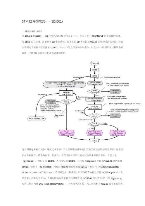
STM32学习笔记——SDIO(1)(2013-02-26 21:45:11)对STM32的SDIO——SD卡输入/输出模块摸索了一下,今天只看了POWER UP这个函数的实现。
对SDIO编写驱动,需要参考SD卡的协议,我手上的SD卡协议是ver2.00的物理层简化协议。
协议主要规定了主机(这里就是STM32)向SD卡写入的各种控制指令,以及SD卡的初始化过程状态转移图。
了解SD卡从初始化状态转移图开始。
这个图看起来有点复杂,感觉无从下手,其实仔细瞧瞧就跟我们数电学的状态转移图差不多,框框里面是各种操作,箭头指向下一步操作,直线引出去的部分就是状态发生跳转的条件。
首先上电(power-on),然后发出CMD0,再接着发送CMD8,有应答(response)判断为Ver2.00或更新的SDMC,无应答(no response)判断为ver2.00或者更新版SDMC(电压不匹配(voltage mismatch) )或ver1.X SDMC或不是SDMC。
若判断为前一种情况,则问询是否为有效应答(valid response),如果不是,判断为无效卡,否则判断为有效卡且开始循环发送ACMD41指令直至SD卡发出power up 应答。
然后判断CCS(card capacity status——卡容量状态)位,为1则判断为ver2.00或者更新的大容量卡(high capacity SD memory card),否则判断为ver2.00或者更新的标准卡(sandard capacity SD memory card)。
至此,power on工作结束。
上文只是对状态图进行了一个解读,真正要控制还是需要知道各个CMD如何发送。
SD卡协议提供了几个CMD的格式以及其响应值的格式(如果有相应的话)。
下面就对函数的具体编写进行下总结。
(1)初始化SDIO利用SDIO_Init中的结构体初始化SDIO接口。
该结构体有以下几个成员函数:SDIO_ClockDiv、SDIO_ClockEdge、SDIO_ClockBypass、SDIO_ClockPowerSave、SDIO_BusWide、SDIO_HardwareFlowControl。
stm32笔记USART整理

stm32笔记USART整理.txt该接口通过3个引脚连接到另外的外部设备上。
任何USART双向通信都至少需要两个引脚:接收数据输入RX和发送数据输出TX当发送器禁能时输出引脚恢复到I/O端口配置。
当发送器使能时且无数据发送,TX引脚为高电平。
字长可以通过设置USART_CR1寄存器中的M位来选择是8位还是9位TX引脚在起始位期间为低,停止位期间为高空闲符被认为是一个全“1”的帧,其后紧跟着包含数据的下一个帧的起始位(“1”的数目包含了停止位的数目)间隙符被认为是一个帧周期都接收到“0”。
在间隙帧之后,发送器插入1个或者2个的停止位(逻辑“1”)来应答起始位发送器发送器可以发送8或者9位的数据字,这取决于M位的状态。
相关时钟脉冲在SCLK引脚输出1、字符发送USART发送期间,TX引脚先出现最低有效位。
这种模式下,USART_DR寄存器包含了一个内部总线和发送移位寄存器之间的缓冲区TDR。
每个字符之前都有一位逻辑低电平的起始位,以可设置数目的停止位结束。
TE位使能之后将发送一个空闲帧2、可配置的停止位1个停止位:这是陌生人的停止位数目2个停止位:常规USART,单线和调制解调器模式下支持0.5个停止位:当处于智能卡模式下接收数据时使用1.5个停止位:当处于智能卡模式下发送数据时使用空闲帧的发送包含了停止位。
间隙帧是10(11)个低位之后跟着配置的停止位配置流程:通过把USART_CR1寄存器中的UE位写1来使能USART->配置USART_CR1寄存器中的M位来定义字长->配置USART_CR2寄存器中的停止位数目->若采用多缓冲通信选择USART_CR3寄存器中的DMA使能位(DMAT),按照多缓冲通信中解释的配置DMA寄存器->设置USART_CR1寄存器中的TE位来发送一个空闲帧来作为第一次发送->通过USART_BRR 寄存器选择期望的波特率->往USART_DR寄存器中写入要发送的数据,这也将清除TXE位。
STM32学习笔记之USART
STM32学习笔记之USARTUSART 功能概述接口通过三个引脚与其他设备连接在一起(见图248)。
任何USART 双向通信至少需要两个脚:接收数据输入(RX)和发送数据输出(TX)。
RX:接收数据串行输。
通过过采样技术来区别数据和噪音,从而恢复数据。
TX:发送数据输出。
当发送器被禁止时,输出引脚恢复到它的I/O 端口配置。
当发送器被激活,并且不发送数据时,TX 引脚处于高电平。
在单线和智能卡模式里,此I/O 口被同时用于数据的发送和接收。
●总线在发送或接收前应处于空闲状态●一个起始位●一个数据字(8 或9 位),最低有效位在前●0.5,1.5,2 个的停止位,由此表明数据帧的结束●使用分数波特率发生器12 位整数和4 位小数的表示方法。
●一个状态寄存器(USART_SR)●数据寄存器(USART_DR)●一个波特率寄存器(USART_BRR),12 位的整数和4 位小数●一个智能卡模式下的保护时间寄存器(USART_GTPR)关于以上寄存器中每个位的具体定义,请参考寄存器描述第节:USART 寄存器描述。
在同步模式中需要下列引脚:●CK:发送器时钟输出。
此引脚输出用于同步传输的时钟,(在Start 位和Stop 位上没有时钟脉冲,软件可选地,可以在最后一个数据位送出一个时钟脉冲)。
数据可以在RX 上同步被接收。
这可以用来控制带有移位寄存器的外部设备(例如LCD 驱动器)。
时钟相位和极性都是软件可编程的。
在智能卡模式里,CK 可以为智能卡提供时钟。
在IrDA 模式里需要下列引脚:●IrDA_RDI: IrDA 模式下的数据输入。
●IrDA_TDO: IrDA 模式下的数据输出。
下列引脚在硬件流控模式中需要:●nCTS: 清除发送,若是高电平,在当前数据传输结束时阻断下一次的数据发送。
voidUSART_SendChar(USART_TypeDef* USARTx, uint16_t Data){ //检测参数assert_param(IS_USART_ALL_PERIPH(USARTx));。
STM32_7816智能卡接口笔记
5.2.4
安全API ....................................................................................................................... 25
6
智能卡接口库:描述...................................................................................................................... 27
4
ISO 7816 – 3 – 电信号和传输协议 ............................................................................................... 10
4.1
智能卡上电启动和重置...................................................................................................... 11
5.2
应用层协议.......................................................................................................................... 19
5.2.1
ISO 7816-4 APDU ....................................................................................................... 20
STM32F101xx 和 STM32F103xx 的智能卡接 说明书口
AN2598
应用笔记
使用 STM32F101xx 和 STM32F103xx 的 智能卡接口
简介 本文叙述了如何使用STM32F10xxx的USART模块实现智能卡接口解决方案,包括固件和硬件接 口的实现。该固件和硬件包的目的是提供相应的资源,使用户使用USART模块的智能卡模式, 更加便捷地开发应用程序。 这个固件接口包括支持ISO 7816-3/4规范的库文件,同时提供基于ST的STM3210B-EVAL和 STM3210E-EVAL评估板的应用程序示例。 本文档及其相关的固件可以从ST的网站下载:
AN2867
ISO7816-3——电信号和传输协议
4 ISO7816-3——电信号和传输协议
IS0 7816-3开始研究智能卡“智能”方面的规范。该标准描述了智能卡和读卡器之间的关系, 其中智能卡作为从设备,读卡器作为主设备。通讯的基础是,读卡器通过触点给智能卡发送信 号,然后智能卡作出回应,如此不断循环交互。
在使能智能卡模式的情况下,必须如下配置USART模块: ● 8位数据位加上奇偶校验 ● 0.5或1.5位停止位
一个5位的预分频器和智能卡时钟发生器为智能卡提供时钟。智能卡接口的其他功能则由软件配 合GPIO口实现。
软件中不处理ISO 7816-3中定义的反向信号传输约定,反转数据和最高有效位优先的情况。
协议
ISO 7816-3标准为异步协议定义了时间基准单位,称作ETU(elementary time units),它与输入 至智能卡的时钟频率有关。一个ETU的长度是一个位时间。USART接收器和发送器在内部通过 Rx_SW信号相连接。必须将USART模块设置为智能卡模式,才能实现从STM32F10xxx向智能 卡传输数据。
- 1、下载文档前请自行甄别文档内容的完整性,平台不提供额外的编辑、内容补充、找答案等附加服务。
- 2、"仅部分预览"的文档,不可在线预览部分如存在完整性等问题,可反馈申请退款(可完整预览的文档不适用该条件!)。
- 3、如文档侵犯您的权益,请联系客服反馈,我们会尽快为您处理(人工客服工作时间:9:00-18:30)。
©2007 MXCHIP Corporation. All rights reserved. 021-52655026/025
5
ISO 7816 – 4 – 智能卡命令 ........................................................................................................... 16
5.1
T0 协议 ............................................................................................................................... 16
1.3
协议........................................................................................................................................ 6
1.4
智能卡时钟发生器................................................................................................................ 7
6.3
怎样发送APDU命令给智能卡 ........................................................................................... 35
6.3.1 6.3.2 6.3.3 6.3.4 6.3.5 6.3.6 6.3.7
应用笔记........................................................................................................................................................... 1
2
智能卡阅读器硬件连接.................................................................................................................... 7
3
ISO 7816:协议概述 ........................................................................................................................ 8
1.1
简介........................................................................................................................................ 5
1.2
外部接口................................................................................................................................ 5
5.2
应用层协议.......................................................................................................................... 19
5.2.1
ISO 7816-4 APDU ....................................................................................................... 20
6.1
文件组织.............................................................................................................................. 27
6.2
智能卡接口库函数.............................................................................................................. 27
6.2.1 6.2.2 6.2.3 6.2.4
SC_Handler function.................................................................................................... 28 SC_PowerCmd............................................................................................................. 32 SC_Reset...................................................................................................................... 33 SC_PTSConfig............................................................................................................. 34
5.2.3
STM32F101xx 和 STM32F103xx 中的智能卡接口
ISO 7816-4 函数 ......................................................................................................... 23
4
ISO 7816 – 3 – 电信号和传输协议 ............................................................................................... 10
4.1
智能卡上电启动和重置...................................................................................................... 11
©2007 MXCHIP Corporation. All rights reserved. 021-52655026/025
目录
STM32F101xx 和 STM32F103xx 中的智能卡接口
AN2598 ........................................................................................................................................................... 1
SC_GET_A2R ............................................................................................................. 35 SELECT_FILE............................................................................................................. 36 SC_GET_RESPONSE ................................................................................................. 36 SC_READ_BINARY ................................................................................................... 37 SC_CREATE_FILE ..................................................................................................... 38 SC_UPDATE_BINARY .............................................................................................. 38 SC_VERIFY ................................................................................................................ 39
3.1
简介........................................................................................................................................ 9