电路分析与电子线路综合训练题(DOC43页)
电路分析模拟试题3套及答案doc资料
《电路理论》1一、填空题1.对称三相电路中,负载Y联接,已知电源相量︒∠=∙0380AB U (V ),负载相电流︒∠=∙305A I (A );则相电压=∙C U (V ),负载线电流=∙Bc I (A )。
2.若12-=ab i A ,则电流的实际方向为 ,参考方向与实际方向 。
3.若10-=ab i A ,则电流的实际方向为 ,参考方向与实际方向 。
4.元件在关联参考方向下,功率大于零,则元件 功率,元件在电路中相当于 。
5.回路电流法自动满足 定律,是 定律的体现6.一个元件为关联参考方向,其功率为―100W ,则该元件 功率,在电路中相当于 。
7.在电路中,电阻元件满足两大类约束关系,它们分别是 和 。
8.正弦交流电的三要素是 、 和 。
9.等效发电机原理包括 和 。
10.回路电流法中自阻是对应回路 ,回路电流法是 定律的体现。
11.某无源一端口网络其端口电压为)302sin(240)(︒+=t t u (V),流入其端口的电流为)602cos(260)(︒-=t t i (A),则该网络的有功功率 ,无功功率 ,该电路呈 性。
若端口电压电流用相量来表示,则其有效值相量=∙U ,=∙I 。
12.无源二端电路N 的等效阻抗Z=(10―j10) Ω,则此N 可用一个 元件和一个 元件串联组合来等效。
13 .LC 串联电路中,电感电压有效值V 10U L =,电容电压有效值V 10U C =,则LC 串联电路总电压有效值=U ,此时电路相当于 。
14.对称三相电路中,当负载△联接,已知线电流为72A ,当A 相负载开路时,流过B 和C 相的线电流分别为 和 。
若A 相电源断开,流过B 和C 相的线电流分别为 和 。
15.对称三相星形连接电路中,线电压超前相应相电压 度,线电压的模是相电压模的 倍。
16 .RLC 并联谐振电路中,谐振角频率0ω为 ,此时电路的阻抗最 。
17 .已知正弦量))(402sin()(1A t t i ︒+=,))(1102cos()(2A t t i ︒+-=,则从相位关系来看,∙1I ∙2I ,角度为 。
电工线路分析考试题及答案
电工线路分析考试题及答案一、选择题(每题2分,共20分)1. 电路的基本组成包括电源、负载和______。
A. 导线B. 开关C. 电阻D. 电容2. 在串联电路中,各电阻两端的电压之和等于______。
A. 电源电压B. 总电阻C. 电流D. 功率3. 欧姆定律表明,电流与电压的关系是______。
A. 正比B. 反比C. 无关D. 有时正比,有时反比4. 并联电路中,各支路的电流之和等于______。
A. 电源电流B. 总电压C. 总电阻D. 电源电压5. 电阻的单位是______。
A. 欧姆B. 安培C. 伏特D. 瓦特6. 电感元件的特点是______。
A. 阻碍电流变化B. 阻碍电压变化C. 阻碍电流和电压变化D. 不阻碍电流和电压变化7. 电容元件的特点是______。
A. 储存电荷B. 消耗电荷C. 阻碍电流D. 产生电流8. 交流电的频率是指______。
A. 每秒电流方向改变的次数B. 电流强度C. 电压大小D. 电流方向9. 三相交流电的相位差是______。
A. 0度B. 30度C. 60度D. 90度10. 功率因数是指______。
A. 有功功率与视在功率的比值B. 无功功率与视在功率的比值C. 有功功率与无功功率的比值D. 视在功率与无功功率的比值答案:1. A2. A3. A4. A5. A6. A7. A8. A9. C10. A二、填空题(每空2分,共20分)1. 电阻的公式为 R = ______ / I,其中 R 代表电阻,I 代表电流。
2. 在串联电路中,总电阻等于各部分电阻之 ______。
3. 电容器的单位是 ______,符号为μF。
4. 电流的国际单位是 ______,符号为 A。
5. 三相交流电的电压相量可以表示为 ______、Vb 和 Vc。
6. 功率因数的提高可以减少 ______ 的损耗。
7. 电路的功率计算公式为P = U × ______。
电路图分析专项训练(新)

电路图分析专项训练(新)1. 简介电路图分析是电子工程领域中的重要基础知识,对于电路设计、故障排除和维修具有重要意义。
本文档旨在提供一种专项训练,帮助研究者加强对电路图的理解与分析能力。
2. 训练目标- 加深对电路图符号和元件功能的理解。
- 学会分析电路图中的电流路径和电压变化。
- 掌握电路图分析的基本方法和步骤。
- 培养解决电路问题时的逻辑思维和问题诊断能力。
3. 训练内容3.1 电路图符号和元件功能- 研究电阻、电容、电感、开关等常见电路元件的符号和功能。
- 了解各种电子元件在电路中的作用和应用。
3.2 电流路径和电压变化分析- 分析电路图中各个路径的电流流向和大小。
- 观察并计算电路元件之间的电压变化。
3.3 电路图分析的基本方法和步骤- 研究如何根据电路图进行正确的分析和推理。
- 掌握基本的电路图分析技巧,如串联、并联、等效电路的转换等。
3.4 问题诊断和解决- 练分析具体电路图中的问题,并进行故障诊断。
- 学会运用所学的电路图分析方法解决实际的电路问题。
4. 训练建议- 从简单电路图开始,逐步深入研究和训练。
- 多进行实践,通过模拟电路环境来加强理论知识的应用能力。
- 参考相关教材和在线资源,扩充研究内容。
5. 结论电路图分析专项训练是提升电子工程技能的重要环节,通过系统的研究和实践,可以帮助研究者掌握电路图分析的基本技巧和解决问题的能力。
建议研究者持续努力,不断提升自己的电路图分析能力。
参考资料:- "电路分析与设计" 作者:张学工,清华大学出版社,2018年。
电路分析试题和答案(全套)

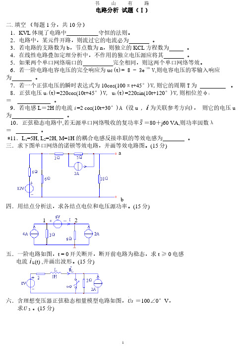
电路分析试题(Ⅰ)二. 填空(每题1分,共10分)1.KVL体现了电路中守恒的法则。
2.电路中,某元件开路,则流过它的电流必为。
3.若电路的支路数为b,节点数为n,则独立的KCL方程数为。
4.在线性电路叠加定理分析中,不作用的独立电压源应将其。
5.若一阶电路电容电压的完全响应为uc(t)= 8 - 3eV,则电容电压的零输入响应为。
7.若一个正弦电压的瞬时表达式为10cos(100πt+45°)V,则它的周期T 为。
8.正弦电压u(t)=220cos(10t+45°)V, u(t)=220sin(10t+120°)V,则相位差φ=。
9.若电感L=2H的电流i =2 cos(10t+30°)A (设u ,为关联参考方向),则它的电压u为。
三.求下图单口网络的诺顿等效电路,并画等效电路图。
(15分)a b四.用结点分析法,求各结点电位和电压源功率。
(15分)1 2五.一阶电路如图,t = 0开关断开,断开前电路为稳态,求t ≥ 0电感电流(t) ,并画出波形。
(15分)电路分析试题(Ⅱ)二. 填空(每题1分,共10分)1.电路的两类约束是。
2.一只100Ω,1w的电阻器,使用时电阻上的电压不得超过 V。
3.含U和I两直流电源的线性非时变电阻电路,若I单独作用时,R 上的电流为I′,当U单独作用时,R上的电流为I",(I′与I"参考方向相同),则当U和I共同作用时,R上的功率应为。
4.若电阻上电压u与电流i为非关联参考方向,则电导G的表达式为。
5.实际电压源与理想电压源的区别在于实际电压源的内阻。
6.电感元件能存储能。
9.正弦稳态电路中, 某电感两端电压有效值为20V,流过电流有效值为2A,正弦量周期T =πS , 则电感的电感量L=。
10.正弦稳态L,C串联电路中, 电容电压有效值为8V , 电感电压有效值为12V , 则总电压有效值为。
11.正弦稳态电路中, 一个无源单口网络的功率因数为0. 5 , 端口电压u(t) =10cos (100t +ψu) V,端口电流(t) = 3 cos(100t - 10°)A (u,i为关联参考方向),则电压的初相ψu为。
电子线路综合练习题三
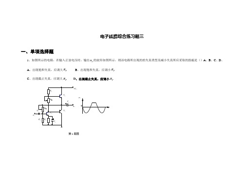
电子线路综合练习题三一、单项选择题1、如图所示的电路,在输入正弦电压时,输出o u 的波形如图所示,则该电路所出现的的失真类型及减小失真所应采取的措施是()A 、B 、C 、D 、 A 、出现饱和失真,应调大P R B 、出现饱和失真,应调小P R C 、出现截止失真,应调大P R D 、出现截止失真,应调小P RR R R R R 112233312C C C V V V +V ccu u ioP 1P2Ou ot第1题图+-u s+V cc+-u o123R R R fff fC C s2第2题图R R R R R 112233312P1P2C C C V V V +V c cu u ioOu ot第3题图2、如图所示的电路中,欲稳定电路的输出电压,应采用的方法是() A 、1与3连接B 、1与4连接C 、2与3连接D 、2与4连接3、如图所示的电路中,输入信号I u 为正弦波,输出o u 的波形如图所示,为减少失真应() A 、调大1P R B 、调小1P R C 、调大2P R D 、调小2P R∞u u io R p5KΩ10KΩ10KΩ第5题图CW7908∞C C IoR R R p 12R L++--U U I o第4题图4、如图所示,三端稳压器采用CW7908,输入 电压I U 足够大,1R =2R =400Ω,P R 的总阻值 也为400Ω,则输出电压Uo 的 可调范围是() A 、-2.67 ~ -5.53V B 、-12 ~ -24V C 、12 ~ 24V D 、2.67 ~ 5.53V5、如图所示的电路,P R 的总阻值也为10K Ω,则电路电压放大倍数IO u u uA 的可调范围是()A 、-1.5 ~ -3VB 、-0 ~ 3VC 、1.5 ~ 3VD 、1 ~ 2VR R R C C C L L 1112223+V c c第6题图第7题图6、如图电路所示,以下说法正确的是()A 、电路不满足振幅平衡条件,故不能自激振荡B 、电路不满足相位平衡条件,故不能自激振荡C 、电路不满足振幅及相位平衡条件,故不能自激振荡D 、电路满足相位平衡条件,且结构合理,故有可能自激振荡7、某组合逻辑电路的输出Y 与AB 的波形如图所示,则该电路的逻辑功能为 A 、与非B 、或非C 、异或D 、同或8、若误用万用表的电流表或电阻挡去测量电路的两点间的直流电压,则()A 、万用表的指针不动B 、万用表测量误差太大C 、万用表读数不稳定D 、可能损伤或烧毁表头9、测得某放大电路中三极管的三个电极对地电位分别是:V 1=-1.5V ,V 2 = -1.5V ,V 3 = -1.5V ,则三个电极的顺序和管型分别为A 、b c e PNP 型B 、b c e NPN 型C 、c b e PNP 型D 、c b eNPN 型 10、在N 型半导体中()A 、只有自由电子B 、只有空穴C 、有空穴也有自由电子D 、以上答案都不对 11、收音机搜索电台,利用的原理是( )A 、自激原理B 、调谐原理C 、蒸馏原理D 、稳压原理 12、场效晶体管是一种( )控制性电子元件 A 、电流B 、电压C 、光D 、磁&&&11ABY13、三端集成稳压器CW7812的输出电压为A 、-12VB 、-24VC 、24VD 、12V14、直接耦合放大器电路存在零点漂移的主要原因是( )A 、电阻阻值B 、参数受温度影响C 、三极管参数的分散性D 、电源电压不稳定15、引入负反馈后,放大器的状态为( ) A 、静态B 、动态C 、开环状态D 、闭环状态 16、LC 正弦波振荡器电路的振荡频率为A 、LCf 10=B 、LC f 10= C 、LCf π210= D 、LC f π210=17、下列逻辑式中,正确的逻辑公式( )A 、AB B A =+ B 、B A B A =+C 、B A B A +=+D 、以上都不对二、填空题1、在图3—3—14所示的电路中,当ωt =Cω1时,电路相当于_________状态。
电子线路试题及答案

电子线路试题及答案### 电子线路试题及答案#### 一、选择题(每题2分,共20分)1. 电阻串联时,总电阻值等于各电阻值之和。
这种说法是()。
- A. 正确- B. 错误2. 一个电路中的电流源可以等效为一个()。
- A. 电压源- B. 电阻- C. 电容3. 在并联电路中,总电阻的倒数等于各并联电阻的倒数之和。
这种说法是()。
- A. 正确- B. 错误4. 一个二极管的正向导通电压通常在()伏特左右。
- A. 0.3- B. 0.7- C. 1.05. 放大电路的基本功能是()。
- A. 整流- B. 滤波- C. 信号放大#### 二、填空题(每题2分,共20分)1. 在电路中,电源的内阻越小,输出的电流能力越()。
2. 一个理想电压源的特点是无论负载如何变化,其输出电压保持()。
3. 欧姆定律的公式是 V = I * R,其中 V 代表()。
4. 一个电路的功率计算公式是 P = V * I,其中 P 代表()。
5. 在分压电路中,各电阻的分压与电阻值成()。
#### 三、简答题(每题10分,共30分)1. 简述整流电路的工作原理及其应用场景。
2. 解释滤波电路的作用,并简述其基本类型。
3. 描述反馈放大电路的基本概念及其优点。
#### 四、计算题(每题15分,共30分)1. 已知一个串联电路中有三个电阻,分别为R1 = 100Ω,R2 = 200Ω,R3 = 300Ω。
求该串联电路的总电阻。
2. 假设有一个并联电路,其中包含两个电阻,R1 = 500Ω 和 R2 = 1000Ω。
求该并联电路的总电阻,并计算当总电压为 10V 时,通过R1 的电流。
3. 给定一个电路,其中包含一个 5V 的理想电压源和一个1000Ω 的电阻。
计算通过电阻的电流,并简述电路的功率。
#### 答案#### 一、选择题1. A2. A3. A4. B5. C#### 二、填空题1. 强2. 恒定3. 电压4. 功率5. 正比#### 三、简答题1. 整流电路将交流电转换为直流电,常用于电源适配器和电池充电器。
电路分析习题.doc
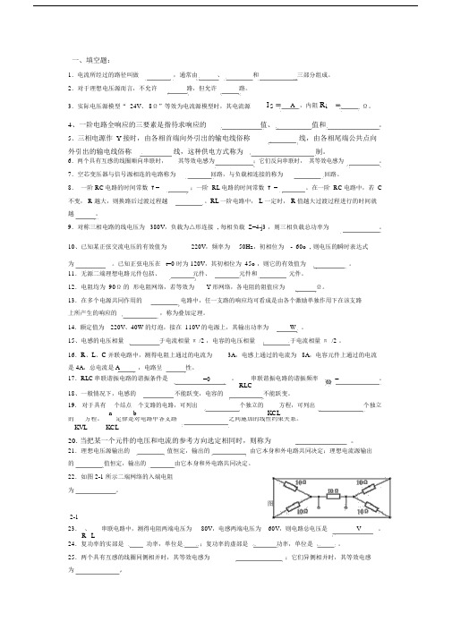
一、填空题:1.电流所经过的路径叫做 ,通常由 、 和 三部分组成。
2.对于理想电压源而言,不允许路,但允许路。
3.实际电压源模型“ 24V 、 8Ω”等效为电流源模型时,其电流源I SA ,内阻 R iΩ。
4、一阶电路全响应的三要素是指待求响应的值、值和。
5、三相电源作 Y 接时,由各相首端向外引出的输电线俗称 线,由各相尾端公共点向外引出的输电线俗称线,这种供电方式称为制。
6.两个具有互感的线圈顺向串联时,其等效电感为;它们反向串联时, 其等效电感为。
7.空芯变压器与信号源相连的电路称为 回路,与负载相连接的称为回路。
8. 一阶 RC 电路的时间常数 τ = ;一阶 RL 电路的时间常数 τ =。
在一阶 RC 电路中,若 C不变, R 越大,则换路后过渡过程越 。
RL 一阶电路中, L 一定时, R 值越大过渡过程进行的时间就越。
9.对称三相电路的线电压为 380V ,负载为△形连接 , 每相负载 Z=4-j3 ,则三相负载总功率为。
10、已知某正弦交流电压的有效值为 220V ,频率为 50Hz ,初相位为 - 60o , 则电压的瞬时表达式为。
已知正弦电压在 t=0 时为 120V ,其初相位为 45o ,则它的有效值为。
11.无源二端理想电路元件包括、 元件、元件和 元件。
12.电阻均为 90Ω的 形电阻网络,若等效为 Y 形网络,各电阻的阻值应为 Ω。
13.在多个电源共同作用的 电路中,任一支路的响应均可看成是由各个激励单独作用下在该支路上所产生的响应的,称为叠加定理。
14. 额定值为 220V 、40W 的灯泡,接在 110V 的电源上,其输出功率为 W 。
15、电感的电压相量于电流相量π /2 ,电容的电压相量于电流相量π /2 。
16.R 、L 、C 并联电路中,测得电阻上通过的电流为 3A ,电感上通过的电流为 8A ,电容元件上通过的电流是 4A ,总电流是A,电路呈性。
17.RLC 串联谐振电路的谐振条件是 =0。
电路分析考试题及答案

电路分析考试题及答案一、单项选择题(每题2分,共20分)1. 电路中,电压与电流相位完全相反的元件是()。
A. 电阻B. 电感C. 电容D. 二极管答案:C2. 在交流电路中,纯电阻电路的功率因数为()。
A. 0B. 0.5C. 1D. -1答案:C3. 电路中,电流的参考方向与实际方向相反时,该电流的值为()。
A. 正值B. 负值C. 不确定D. 零答案:B4. 电路中,若电阻R1和R2并联,则总电阻R的计算公式为()。
A. R = R1 + R2B. R = R1 * R2 / (R1 + R2)C. 1/R = 1/R1 + 1/R2D. R = R1 * R2答案:C5. 电路中,理想电压源与理想电流源不能()。
A. 串联B. 并联C. 直接替换D. 混合使用答案:C6. 电路中,RLC串联电路的谐振频率f0计算公式为()。
A. f0 = 1/(2π√(LC))B. f0 = 1/(2π√(L/C))C. f0 = 1/(2π√(R/L))D. f0 = 1/(2π√(R/C))答案:A7. 电路中,三相电路的星形接法中,线电压与相电压的关系为()。
A. U线 = U相B. U线= √3 * U相C. U线 = 2 * U相D. U线= √2 * U相答案:B8. 电路中,若要测量交流电路中的功率,应使用()。
A. 直流电压表B. 直流电流表C. 交流电压表D. 功率表答案:D9. 电路中,二极管正向导通时的电压降约为()。
A. 0.7VB. 1.5VC. 3VD. 5V答案:A10. 电路中,若要实现电压放大,应使用()。
A. 电阻B. 电容C. 电感D. 三极管答案:D二、填空题(每题2分,共20分)1. 电路中,欧姆定律的数学表达式为 V = ________。
答案:IR2. 电路中,电容器的容抗计算公式为 Xc = ________。
答案:1/(2πfC)3. 电路中,电感器的感抗计算公式为 Xl = ________。
电路分析考试题和答案

电路分析考试题和答案一、单项选择题(每题2分,共20分)1. 电路中,电压和电流的参考方向可以任意选择,但必须保持一致。
()A. 正确B. 错误答案:A2. 在串联电路中,各元件的电流是相等的。
()A. 正确B. 错误答案:A3. 欧姆定律适用于直流电路和交流电路。
()B. 错误答案:B4. 理想电压源的内阻为零,理想电流源的内阻为无穷大。
()A. 正确B. 错误答案:A5. 在并联电路中,各支路的电压是相等的。
()A. 正确B. 错误答案:A6. 基尔霍夫电压定律适用于任何闭合回路。
()B. 错误答案:A7. 理想变压器的原副线圈匝数比等于电压比。
()A. 正确B. 错误答案:B8. 电容器的容抗与频率成正比。
()A. 正确B. 错误答案:B9. 电感器的感抗与频率成反比。
()B. 错误答案:B10. 交流电路中的功率因数是电压与电流相位差的余弦值。
()A. 正确B. 错误答案:A二、填空题(每题2分,共20分)1. 电路中,电压和电流的参考方向可以任意选择,但必须保持______。
答案:一致2. 在串联电路中,各元件的______是相等的。
答案:电流3. 欧姆定律的公式为 V = IR,其中 V 代表______,I 代表电流,R 代表电阻。
答案:电压4. 理想电压源的内阻为______,理想电流源的内阻为无穷大。
答案:零5. 基尔霍夫电流定律适用于任何______。
答案:节点6. 理想变压器的原副线圈匝数比等于______比。
答案:电流7. 电容器的容抗公式为 Xc = 1/(2πfC),其中 f 代表______,C 代表电容。
答案:频率8. 电感器的感抗公式为XL = 2πfL,其中 f 代表频率,L 代表______。
答案:电感9. 交流电路中的功率因数是电压与电流相位差的______值。
答案:余弦10. 电路中的功率 P 可以表示为 P = VI,其中 V 代表电压,I 代表______。
电子线路试题及参考答案
用逻辑抽象掉的。但是到了二十世纪,随着科学实验的发展,特别 是在微观物理学的研究领域中, 由于微观物理的特殊本性以及观测 仪器与被观测系统之间不可避免的干扰的存在, 主体在认识过程中 的巨大的能动作用已成为现代科学方法的一个基本特点。 经典物理学时期,也是科学注重于本体论的探索的时期,人们 把“现象-规律-实体”作为把科学研究向纵深推进的基本线索。这 无疑是一种有效的方法, 今后也还会继续发挥其认识的作用, 不过, 在现代物理学的研究中,人们更注重于关系和模型,这是一个能动 的认识论的时代,一些学者认为,把西方科学中的重视实体,强调 经验、分析和定量表述的方法与中国传统哲学中重视关系,强调整 体、协调和转化的思想结合起来,将会导致一种更加符合我们时代 的科学精神的新的自然面和科学认识方法。 科学活动更加社会化和体制化的趋势, 在物理学研究中也体 现出来,十九世纪前期,科学的进步基本上是通过科学家个人的自 由研究实现的,然而,由于工业革命的发展、生产规模的扩大和科 学作用的增强,从十九世纪下半叶开始,科学活动日益集中于工业 实验室、高等学校以及专门的机构中 ,二十世纪以来,特别是两 次世界大战中各种新式武器的研制以及作战计划的研究方面的惊 人成果, 更引起产业界、 军界和政府对维持和推进科学研究的重视, 全面推动科学和技术的振兴,已经成为各国的基本国策。特别是由 于原子能科学、航天技术、高能物理、极地考察等“大科学”的出
但是, 科学技术的长期发展也导致了一些人们最初的不曾料到 的结果。由于生产的盲目发展,造成了环境污染,生态失调,自然 资源过度消耗;一些发达国家还出现了经济危机,失业增加,犯罪 率提高等社会问题;原子能的实际应用,最初却是以毁灭性的杀人 武器的形式出现的,重大的技术突破却加剧了军备竞赛的进 行。……这些问题当然不能归罪于科学本身,其中有一些问题只能 靠社会制度的合理化和生产管理的科学化去解决; 另一些问题又是 可以靠科学的力量去解决或部分解决的,现代科学对生态系统、环 境治理和资源合理利用的研究, 将加深人们对人类与自然环境的相 互关系的规律的认识, 推进社会的科学化, 协调人类同自然的关系, 使人类能够获得更大的自由。可以预料,随着科学技术的进一步发 展,生产力的巨大提高、人类智力的充分解放以及社会制度的根本 改造都会达到新的水平。 科学在人类全面改造整个社会生活中的作 用,必将更加充分地发挥出来。
电路分析试题库~各章节内容超级全(含答案~)
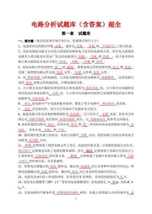
电路分析试题库(含答案)超全第一章 试题库一、填空题(建议较易填空每空0.5分,较难填空每空1分)1、电流所经过的路径叫做 电路 ,通常由 电源 、 负载 和 中间环节 三部分组成。
2、实际电路按功能可分为电力系统的电路和电子技术的电路两大类,其中电力系统的电路其主要功能是对发电厂发出的电能进行 传输 、 分配 和 转换 ;电子技术的电路主要功能则是对电信号进行 传递 、 变换 、 存储 和 处理 。
3、实际电路元件的电特性 单一 而 确切 ,理想电路元件的电特性则 多元 和 复杂 。
无源二端理想电路元件包括 电阻 元件、 电感 元件和 电容 元件。
4、由 理想电路 元件构成的、与实际电路相对应的电路称为 电路模型 ,这类电路只适用 集总 参数元件构成的低、中频电路的分析。
5、大小和方向均不随时间变化的电压和电流称为 稳恒直流 电,大小和方向均随时间变化的电压和电流称为 交流 电,大小和方向均随时间按照正弦规律变化的电压和电流被称为 正弦交流 电。
6、 电压 是电路中产生电流的根本原因,数值上等于电路中 两点电位 的差值。
7、 电位 具有相对性,其大小正负相对于电路参考点而言。
8、衡量电源力作功本领的物理量称为 电动势 ,它只存在于 电源 内部,其参考方向规定由 电源正极高 电位指向 电源负极低 电位,与 电源端电压 的参考方向相反。
9、电流所做的功称为 电功 ,其单位有 焦耳 和 度 ;单位时间内电流所做的功称为 电功率 ,其单位有 瓦特 和 千瓦 。
10、通常我们把负载上的电压、电流方向称作 关联 方向;而把电源上的电压和电流方向称为 非关联 方向。
11、 欧姆 定律体现了线性电路元件上电压、电流的约束关系,与电路的连接方式无关; 基尔霍夫 定律则是反映了电路的整体规律,其中 KCL 定律体现了电路中任意结点上汇集的所有 支路电流 的约束关系, KVL 定律体现了电路中任意回路上所有 元件上电压 的约束关系,具有普遍性。
电路分析模拟试题3套及答案PDF.pdf
V。
3.含 US 和 IS 两直流电源的线性非时变电阻电路,若 IS 单独作用时, R 上的电流为 I′,
当 US 单独作用时,R 上的电流为 I",(I′与 I"
参考方向相同),则当 US 和 IS 共同作用时,R 上的功率应为
。
4.若电阻上电压 u 与电流 i 为非关联参考方向,则电导 G 的表达式
1
书山有路
*七. 含空心变压器正弦稳态电路如图,uS(t)=10 2 cos ( 5t + 15°)V,
求电流i 1(t), i 2(t)。(15 分)
电路分析 试题(Ⅱ)
一.单项选
D.10∠180°V
二. 填空 (每题 1 分,共 10 分)
1.电路的两类约束是
。
2.一只 100Ω,1w 的电阻器,使用时电阻上的电压不得超过
解得: I1 = 1A
I2 = -2A
6
书山有
P4
=
(I1
− I2)2 4
=
(1+ 2)2 4
=
9W 4
六 .解: t < 0 , u C(0-) = - 2V
t > 0 , u C (0+) = u C (0-) = -2V
u C (∞) = 10 – 2 = 8V τ= (1 + 1) 0.25 = 0.5 S
= 1A
电压源单独作用
I3
=
−
6
24 + 3//
6
=
−3A
I2
=
I3
6
6 +
3
=
−3
2 3
=
−2 A
I1 =- I2 =2A
电子线路试题及答案

电子线路试题及答案 It was last revised on January 2, 2021电工与电子技术试题一、填空题(每空1分)1、若各门电路的输入均为A和B,且A=0,B=1;则与非门的输出为_________,或非门的输出为_________。
2、一个数字信号只有________种取值,分别表示为________ 和 ________ 。
3、模拟信号是在时间与幅值上________ 的,数字信号在时间与幅值上是________的。
4、根据逻辑功能的不同特点,逻辑电路可分为两大类: ________ 和 ________。
5、二进制数A=1011010;B=10111,则A-B=____。
6、组合逻辑电路的输出仅仅只与该时刻的 ________ 有关,而与________ 无关。
7、将________变成________ 的过程叫整流。
8、在单相桥式整流电路中,如果负载平均电流是20A,则流过每只晶体二极管的电流是______A。
9、单相半波整流电路,已知变压器二次侧电压有效值为22V,负载电阻RL=10Ω,则整流输出电压的平均值是______;流过二极管的平均电流是______;二极管承受的最高反向电压是______。
10、三极管是________控制元件,场效应管是________控制元件。
11、逻辑函数Y=(A+B)(B+C)(C+A)的最简与或表达式为 _______。
12、三极管输入特性曲线指三极管集电极与发射极间所加电压V CE一定时,与之间的关系。
13、作放大作用时,场效应管应工作在区。
14、放大电路的静态工作点通常是指__、和_。
15、某三级放大电路中,测得Av1=10,Av2=10,Av3=100,总的放大倍数是_。
16、已知某小功率管的发射极电流IE=,电流放大倍数=49,则其输入电阻rbe=。
17. 画放大器的直流通路时应将电容器视为 。
18. 放大器外接一负载电阻RL 后,输出电阻ro 将。
电子线路综合测试卷(一)
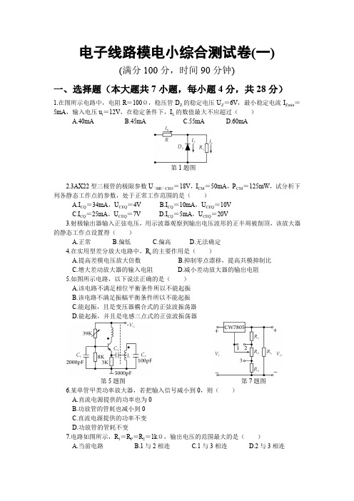
电子线路模电小综合测试卷(一)(满分100分,时间90分钟)一、选择题(本大题共7小题,每小题4分,共28分)1.在图所示电路中,电阻R=100Ω,稳压管D Z的稳定电压U Z=6V,最小稳定电流I Zmin=5mA,输入电压u i=12V,在稳定条件下,I L的数值最大不应超过()A.40mAB.45mAC.55mAD.60mA第1题图2.3AX22型三极管的极限参数U(BR)CEO=18V,I CM=50mA,P CM=125mW,试分析下列各静态工作点的参数,处于正常工作范围的是()A.I CQ=34mA,U CEQ=4VB.I CQ=10mA,U CEQ=10VC.I CQ=25mA,U CEQ=7VD.I CQ=5mA,U CEQ=20V3.射极输出器输入正弦电压,用示波器观察到输出电压波形的正半周被削顶,该放大器的静态工作点设置得()A.正常B.偏低C.偏高D.无法确定4.在实用型差分放大电路中,R e的主要作用是()A.提高差模电压放大倍数B.抑制零点漂移,提高共模抑制比C.增大差动放大器的输入电阻D.减小差动放大器的输出电阻5.如图所示电路,以下说法正确的是()A.该电路不满足相位平衡条件所以不能起振B.该电路不满足振幅平衡条件所以不能起振C.能起振,且是变压器耦合式的正弦波振荡器D.能起振,并且是电感三点式的正弦波振荡器第5题图第7题图6.某单管甲类功率放大器,若把输入信号减小到0,则()A.直流电源提供的功率也为0B.功放管的管耗也减小到0C.直流电源提供的功率不变D.功放管的管耗不变7.电路如图所示,R1=R P=R2=1kΩ,输出电压的范围最大的是()A.当前电路B.1与2相连C.1与3相连D.2与3相连二、是非题(本大题共5小题,每小题2分,共10分,正确填A,错误填B)8.对于NPN三极管,当U BE>0,U BE>U CE,则该管的工作状态是饱和状态。
()9.在NPN三极管共发射极放大电路中,若输出信号负半周平顶,则该放大器发生饱和失真。
电路分析模拟试卷

电路分析模拟试卷(8套)(总40页)--本页仅作为文档封面,使用时请直接删除即可----内页可以根据需求调整合适字体及大小--模拟题1一、选择题:(每小题5分,共35分)1. 图1-1中的电流=I ( )。
A )4A B )6A C )8A D )10A2. 图1-2中的电压=x U ( )。
A )-1V B )0V C )1V D )2V3. 图1-3所示单口网络的输入电阻=ab R ( )。
A )L R B )o R R L // C )L R )1(β+ D )o R β5ΩΩO4. 图1-4所示为一含源单口网络,其戴维南等效电路的等效参数为( )。
A)5V ,2k Ω B )10V ,Ω C )10V ,2k Ω D )20V ,Ω5. 图1-5所示电路已处于稳态。
在0=t 时,开关k 闭合,则=+)0(i ( )。
A)5A B)-2A C)3A D)7A6. 图1-6所示为一正弦稳态电路的一部分,各并联支路中的电流表的读数分别为:A A 14:1,A A 6:2,A A 15:3,A A 25:4,则电流表A 的读数为( )。
A )50AB )10AC )A 210D )A 2157. 已知某单口网络的端口电压和电流分别为:V o )201000cos(10)(-=t t u ,V o )501000cos(5)(-=t t i ,则该单口网络的有功功率和无功功率分别为( )。
A )W,25Var 325B )W,-25Var 325C )W,12.5Var 35.12D )W,-12.5Var 35.12C图1-5二、 二、填空题:(每小题5分,共35分)1. 图2-1所示电路中3Ω电阻吸收的功率=P 。
2. 图2-2所示RL 电路的时间常数为 。
3. 图2-3所示互感电路中,A te i i 3212,0==,则=)(1t u 。
4. 图2-4所示GLC 并联电路,电源频率kHz 650=f ,为使电路发生谐振,电容=C。
(word完整版)电路分析模拟试卷及答案,推荐文档

Is50Ω50Ω2U +-电路分析基础模拟试卷1一、单项选择题:(共10小题,每小题3分,共30分)1. 如图1所示电路中,已知U 2/U 1=0.25,试确定 R x 值是( B )。
A . 50Ω B . 100Ω C . 200Ω D . 25Ω。
图1 图2 2. 如图2所示电路中A 点电压等于( D )。
A.0VB. 56VC.25VD.28V 3. 图3中a 、b 间的等效电阻是( A )Ω。
A. 1.5 B. 4 C. 6 D. 8图3 图4所示,电路换路前处于稳态,t=0时K 打开,则()0c u +=4. 如图4( C )V 。
A. 2S U B . S U - C . S U D . 0 5. 如图5所示的电流i(t)的相量表示(以余弦函数为表达函数)是( D )。
2R36ΩA.10/45°B. 210/135° C. 210/-135° D. 10/135°图5 图66. 已知图6电流表 A1 为10A,电流表 A2 为10A, 电流表 A3 为10A ,则电流表 A为( C )A。
A.30B. 20C. 10D. 07. 在正弦稳态电路中的电感器上,电流i与电压u L为关联参考方向,则下列表达式中正确的是( D )。
A.LiuLω=B.LUIω••=C. LLUjBI••=D.LUI Lω=8. 如图7所示的两个线圈的同名端为( A )。
A.a, d B. a, cC. a, bD. b, d9. 如图8所示电路,该电路的谐振角频率是( C )/rad s。
A. 5510⨯ B. 8510⨯ C. 6510⨯ D. 7510⨯10. 如图9所示电路,双口网络的22Z为( B )Ω。
A. 20B. 40C. 202D. 60图7 图8 图9二、填空题:(共20空,每空1分,共20分)1. 如图10所示电路,理想电压源输出的功率是 12 W 。
电子线路试题及答案

电子线路试题及答案一、选择题(每题2分,共20分)1. 在电路中,电流的参考方向与实际方向相反时,电流的值为:A. 正值B. 负值C. 零D. 无法确定2. 欧姆定律表达式为:A. V = IRB. V = IR + V0C. I = V/RD. R = V/I3. 一个电路的总电阻为10Ω,当并联一个5Ω的电阻后,总电阻将:A. 增加B. 减小C. 保持不变D. 无法确定4. 电容元件在直流电路中相当于:A. 开路B. 短路C. 电阻D. 电感5. 正弦波信号的频率为50Hz,其周期为:A. 0.01秒B. 0.02秒C. 0.1秒D. 1秒二、填空题(每空2分,共20分)6. 根据基尔霍夫电压定律,一个闭合电路中,沿任一闭合路径的电压之和等于______。
7. 串联电路中,总电阻等于各个分电阻的______。
8. 电感元件在交流电路中会产生______。
9. 理想电容元件的电流与电压相位差为______。
10. 一个电路的功率因数是______与有功功率的比值。
三、简答题(每题10分,共30分)11. 解释什么是叠加定理,并给出一个应用叠加定理的例子。
12. 什么是戴维南定理?它在电路分析中有何应用?13. 说明什么是谐振频率,并解释LC谐振电路的工作过程。
四、计算题(每题15分,共30分)14. 给定一个由三个电阻串联组成的电路,R1=100Ω,R2=200Ω,R3=300Ω,求电路的总电阻。
15. 一个RLC串联电路,R=1000Ω,L=100mH,C=10μF,信号频率为50Hz,求电路的阻抗和相位角。
电子线路试题答案一、选择题1. B(负值)2. A(V = IR)3. B(减小)4. A(开路)5. B(0.02秒)二、填空题6. 零7. 总和8. 感抗9. -90度10. 视在功率三、简答题11. 叠加定理是指在一个线性电路中,任何一条支路的电压或电流都可以看作是由电路中每一个独立电源单独作用时在该支路产生的电压或电流的代数和。
电子线路试题及答案
电子线路试题及答案一、单项选择题(每题2分,共20分)1. 在数字电路中,以下哪个不是基本逻辑门?A. 与门B. 或门C. 非门D. 异或门答案:C2. 以下哪个不是模拟信号的特点?A. 连续变化B. 可以数字化C. 可以无限精确D. 可以被模拟电路处理答案:B3. 晶体管的放大作用主要依靠其哪个区域?A. 发射区B. 基区C. 集电区D. 所有区域答案:B4. 在电子电路中,以下哪个元件不是被动元件?A. 电阻B. 电容C. 电感D. 晶体管答案:D5. 以下哪个不是数字电路的特点?A. 离散值B. 抗干扰能力强C. 易于集成D. 频率响应宽答案:D6. 以下哪个不是电子电路中的电源?A. 直流电源B. 交流电源C. 电池D. 电感答案:D7. 在电子电路中,以下哪个元件用于隔离直流?A. 电阻B. 电容C. 电感D. 二极管答案:D8. 以下哪个不是电子电路中的信号类型?A. 模拟信号B. 数字信号C. 光信号D. 声音信号答案:D9. 以下哪个不是电子电路中的放大器类型?A. 运算放大器B. 功率放大器C. 信号放大器D. 逻辑放大器答案:D10. 在电子电路中,以下哪个元件用于限制电流?A. 电阻B. 电容C. 电感D. 二极管答案:A二、多项选择题(每题3分,共15分)1. 以下哪些元件可以用于滤波?A. 电阻B. 电容C. 电感D. 二极管答案:B、C2. 以下哪些是模拟电路的特点?A. 信号连续变化B. 信号离散变化C. 频率响应宽D. 抗干扰能力弱答案:A、C3. 以下哪些元件可以用于整流?A. 电阻B. 二极管C. 电容D. 电感答案:B4. 以下哪些是数字电路的优点?A. 抗干扰能力强B. 易于集成C. 频率响应宽D. 易于实现复杂逻辑答案:A、B、D5. 以下哪些是晶体管的类型?A. NPNB. PNPC. 场效应D. 双极型答案:A、B、C三、填空题(每题2分,共20分)1. 在数字电路中,逻辑“与”操作的输出只有在所有输入都为________时才为高电平。
电路分析与电子线路综合训练题
2018年《电路分析与电子线路》综合训练题注意:2018年《电路分析与电子线路》综合训练组队共同讨论完成综合训练题目3-4题,以书面形式撰写报告,需要详细的讨论过程和仿真的结果。
请同学们自学“数值分析软件(如MATLAB等)及电路仿真软件(如Multisim或Pspice等)”。
提交书面报告时间:6月20日前。
Project 1Power SuppliesObjective: This project will show some of the basic principles of power supplies using fullwave rectifier, Zener diode, and fixed-voltage regulator circuits.Components: Bridge Rectifier (50 PIV, 1 A), Zener diode (10 V at 500 mW), 7805 regulatorIntroduction:Most of the direct current (DC) power used in electronic devices is derived by converting 60 Hz, 115 V alternating current (AC) power to direct current power. This AC to DC conversion usually involves a step-down transformer, rectifier, filter, and a regulator. The step-down transformer is used to decrease the AC line voltage from 115 V RMS to an RMS value near the DC voltage needed. The output of the step-down transformer is then fed into a diode rectifier circuit that only outputs positive halves of the input sinusoid. A filter is then used to smooth the rectifier output to achieve a nearly constant DC voltage level. A regulator can be added after the filter to ensure a constant output voltage in spite of changes in load current and input voltages.Two different types of voltage regulators will be used in this project. The first involves a Zener diode circuit and the second involves a voltage regulator circuit. A Zener diode can be used as a voltage regulator when the diode is reverse biased and operated in the breakdown region. To maintain voltage regulation, the Zener diode must be operated in the breakdown region at a current greater than the "knee" current (I ZK). Forcurrents greater than I ZK, the Zener diode characteristic curve is nearly vertical and the voltage across the diode changes very little. Of course there is a maximum current the diode can tolerate, so good regulation is provided when the diode is reverse biased with currents between I ZK and I ZMAX. Zener diodes are available with a wide variety of breakdown voltages. Another type of voltage regulator is available with the 7800 series regulators. This series of fixed-voltage regulators is numbered 78xx, where xx corresponds to the value of the output voltage. Output voltages from 5 to 24 volts are available. These regulators are easy to use and work very well.Design:1. Find approximations for the DC voltage level and AC peak to peak ripple voltage for the bridge rectifier and filter circuit of Figure 1-1.2. For the Zener diode regulator circuit of Figure 1-2 assume that the Zener diode will regulate at 10 V over a current range of 5 mA to 25 mA. Assuming that the current flowing through R is always between 5 mA and 25 mA and the Zener diode is regulating at 10 V, find the minimum values of R and R L required. You may assume the forward diode drop for the two diodes is 1 V.Lab Procedure:1. Construct the bridge rectifier circuit of Figure 1-1 without the capacitor. Use the Variac with the step-down transformer for the input voltage to the bridge rectifier. With the transformer plugged into the Variac, adjust the Variac until the secondary voltage from the transformer equals 12 V RMS. BE CAREFUL not to short the secondary terminals!Observe the secondary waveform on the oscilloscope. Put the oscilloscope on DC coupling and observe the load voltage waveform V L. Remember that both the input source and the load cannot share a common ground terminal.2. Remove power from the circuit. Insert the capacitor as shown in Figure 1-1 being sure to observe the correct polarity. Energize the circuit. With the oscilloscope on DC couplingobserve V L. Measure the DC voltage level using the digital voltmeter. With the oscilloscope on AC coupling observe the ripple voltage V R. Compare these measured values with the calculated values.3. Observe the effect of loading on the circuit by changing the load resistor from 1 kto 500 . Measure the DC voltage level with the digital voltmeter. Observe the ripple voltage with the oscilloscope set on AC coupling. Compare these values with the previously recorded values.4. Record the Zener diode characteristic curve from the digital curve tracer. Note the value of the breakdown voltage in the breakdown region. Also note the value of the "knee" current I ZK.5. After verifying your designed values for R and R L with the instructor, construct the Zener diode regulator circuit of Figure 1-2. Measure the DC voltage level with the digital voltmeter for the minimum value of R L along with several values above and below the minimum value. Be careful not to overload the Zener diode. Comment on the circuit's operation for these different load resistances.6. Construct the 7805 regulator circuit of Figure 1-3 being careful to observe the correct pin configuration of the regulator. Measure the load voltage for R L equal to 300 , 200 , and 100 . Calculate the current for each of these cases. Does the value of the load resistor affect the output voltage?7. Using R L equal to 200 , record the 7805 regulator input voltage (pin 1) and output voltage (pin 3). Decrease the regulator input voltage by decreasing the setting of the Variac. For each decrease in amplitude, record the regulator input and output voltages. Continue decreasing theamplitude until the output of the regulator drops a measurable amount below 5 V. What is the minimum input voltage needed for the 7805 regulator to produce a 5 V output?Questions:1. Why can't the input source and load have a common ground in the bridge rectifier circuit?2. Can the Zener diode be used as a conventional diode? Explain your answer and verify with a curve from the curve tracer.3. Would the value of the output filter capacitor have to increase, decrease, or remain the same to maintain the same ripple voltage if the bridge rectifier were changed to a half-wave rectifier? Explain your answer.4. How would increasing the frequency of the input source affect the ripple voltage assuming all components remained the same?Project 2Analog Applications of the Operational AmplifierObjective:This project will demonstrate some of the analog applications of an operational amplifier through a summing circuit and a bandpass filter circuit.Components: 741 op-ampIntroduction:Figure 2-1 shows a weighted summer circuit in the inverting configuration. This circuit can be used to sum individual input signals with a variable gain for each signal. The virtual ground at the inverting input terminal of the op-amp keeps the input signals isolated from each other. This isolation makes it possible for each input to be summed with a different gain.The bandpass filter shown in Figure 2-2 uses an op-amp in combination with resistors and capacitors. Since the op-amp can increase the gain ofthe filter, the filter is classified as an active filter. This bandpass filter circuit is extremely useful because the center frequency can be changed by varying a resistor instead of changing the values of the capacitors. The center frequency is given by:The center frequency can be changed by varying the variable resistor R3. Increasing R3 decreases the center frequency while decreasing R3 increases the center frequency. The bandwidth is given by:Notice that the bandwidth is independent of the variable resistor R3 so the center frequency may be varied without changing the value of the bandwidth. The gain at the center frequency of the bandpass filter is given by:Design:1. Find the relationship between the output and inputs for the weighted summer circuit of Figure 2-1.2. Design a bandpass filter with a center frequency of 2.0 kHz and a bandwidth of 200 Hz. Let the voltage gain at the center frequency be 20. Check your design with PSPICE®. Use ± 15 V supplies for the op-amp. Use R L = 2.4 k.Figure 2 - 1: Weighted SummerFigure 2 - 2: Bandpass FilterLab Procedure:1. Construct the summing amplifier of Figure 2-1. Design for the transfer function to be V O = -2 V IN1 - V IN2. Use ± 15 V supplies for the op-amp. Use R L = 2.4 k.2. Let V IN1be a 1 V peak sine wave at 1 kHz and V IN2equal to 5 V DC. Verify the amplifier's operation by monitoring the output waveform on the oscilloscope.3. Construct the bandpass filter of Figure 2-2. Use the designed values for the resistors and capacitors. Use ±15 V supplies for the op-amp. Use R L = 2.4 k.4. Record and plot the frequency response (you may want to use computer control for the sweep and data collection). Find the center frequency, corner frequencies, bandwidth, and center frequency voltage gain to verify that the specifications have been met.5. Change R3to lower the center frequency from 2.0 kHz to 1.0 kHz. Repeat part 4 for the new frequency response. Verify that the new center frequency is 1.0 kHz. What is the new bandwidth? What is the new center frequency voltage gain? Compare with the measurements of Procedure 4.Questions:1. Could the summer circuit be used with the inputs connected to the noninverting terminal and produce the same affect without the inversion? Explain.2. What is/are the benefit(s) of using an op-amp circuit to produce a bandpass filter over using an RLC circuit with a noninverting op-amp at the output of the RLC circuit?Project 3Analog Computer Applications using the Operational AmplifierObjective:This project will focus on the use of the operational amplifier in performing the mathematical operations of integration and differentiation. The design of a simple circuit (analog computer) to solve a differential equation will also be included.Components: 741 op-ampIntroduction:Figures 3-1 and 3-2 illustrate two op-amp based circuits designed to perform differentiation and integration respectively. The operations are performed "real-time" and can be helpful in observing both initial transients and steady state response. The analysis of the circuits is based on the "ideal" op-amp assumptions and performed in the time domain. The resistor R I shown in the two circuits is included to help with stability and for general circuit protection. The value for R I is nominally set equal to the feedback resistor (Figure 3-1) or the input resistor (Figure 3-2). The purpose of the optional resistor is left for student investigation in conjunction with the summary questions.The differentiator and integrator circuits may be combined with "standard" inverting and non-inverting op-amp circuits to provide the building blocks for analog computers. The resultant analog computer circuits are designed to solve differential and/or integral/differential equations in a real time environment. The ability to easily include, and change, initial conditions and forcing functions are additional benefits of the analog computers. Figure 3-3 illustrates a circuit designed to solve the second order differential equation KY- Y = 0 with the initial condition Y(0) = - V X and K = R1R2C1C2. The initial condition is "set" by using the momentary contact switch to force the output to equal the applied voltage at t = 0 (the time the switch is closed).While the major advances in digital computers and digital signal processing have reduced the use of these three circuits, they are still a fast and relatively inexpensive method for process control and stability/operation analysis for systems that can be represented in terms of differential equations.Design:1. Derive the expressions relating the input and output signals for the circuits shown in Figures 3-1 and 3-2.2. Design an analog computer to solve with y(0) = 2. Solve the differential equation when f(t) = 0 and verify your results using PSpice®.Figure 3 - 1: DifferentiatorFigure 3 - 2: IntegratorFigure 3 - 3: Analog Computer (linear, second order, homogenousdifferential equation)Lab Procedure:1. Construct the circuit shown in Figure 3-1. Use ± 15 V supplies for the op-amp and a load resistance of2.4 k.2. Verify the operation of the circuit using a 500 mV peak, 50 Hz sinewave as the input signal. Be sure to design the "gain" such that the output does not saturate.3. Repeat step 2 with a sinewave frequency of 500 Hz. Does the circuit still operate correctly? What changes need to be made to prevent output saturation?4. Repeat steps 2 and 3 using a triangle wave and then using a square wave with the same magnitudes and frequencies as used in steps 2 and 3.5. Construct the circuit shown in Figure 3-2. Again, use ±15 V supplies for the op-amp and a load resistance of 2.4 k.6. Repeat steps 2 through 4 for this circuit. Be sure to adjust your "gain" as necessary to maintain an output signal within the saturation limits of ± 12 V.7. Construct the circuit designed to solve the differential equation in part 2 of the design section. Verify the operation of the design using three different input waves (sine, triangle, and square). Determine the operation for at least three differentfrequencies -- 10 Hz, 1 kHz, and 100 kHz. Explain any differences in operation of the circuit. What affect does the initial condition have on the result?Questions:1. How could you use the differentiator to obtain an estimate of the slew rate for the op-amp?2. Why should you include a resistor in parallel with the capacitor in the integrator?3. What is the purpose of the resistor in series with the input capacitor in the differentiator?4. Is it possible to design a circuit to perform the differentiation and integration functions using the non-inverting input? Explain your answer.Project 4Common Emitter Amplifier(designed for two lab periods)Objective: This project will show how the h-parameters for a BJT can be measured and used in an equivalent circuit model for the BJT. A CE small signal amplifier will be biased and designed to specifications along with both low and high frequency response and adjustment. Series-series feedback will also be used to control the bandwidth and input impedance of the CE amplifier.Components: 2N2222 BJTIntroduction:In order for circuits involving transistors to be analyzed, the terminal behavior of the transistor must be characterized by a model. Two of the models often used for a BJT are the hybrid- and the h-parameter models. The complete hybrid-circuit model for the BJT is shown in Figure 9-1. This model includes the internal capacitances and output resistance of the BJT. Inclusion of the internal transistor capacitances makes the hybrid- model valid throughout the entire frequency range of the transistor. Typical data sheet values of C and C are 13 pF and 8 pF respectively. These values are so small that C and C may be considered open circuits for midband frequencies. The resistance r x typically has a value in the tens of ohms and can be considered a short circuit while r and r o are usually extremely large in value and can be considered open circuits.The h-parameter small signal model for the BJT is characterized by the four h-parameters and is shown in Figure 9-2. Unlike the hybrid-model, the h-parameter model does not ordinarily include frequency related effects and components and is therefore generally valid only at midband frequencies and below . However the h-parameter model is very useful sincethe h-parameters can be easily measured for a BJT. The value of h re is usually on the order of 10-4 and can be considered a short circuit. The value of h oe is usually on the order of 10-5 S making 1/h oe effectively an open circuit for most circuit configurations and biases. Making the same assumptions, the hybrid-and h-parameter models are equivalent at midband frequencies.For a transistor to operate as an amplifier, it must have a stable bias in the active region. To bias a transistor, a constant DC current must be established in the collector and emitter. This current should be as insensitive as possible to variations in temperature and (or h fe). The voltage across the base-emitter junction decreases about 2 mV for each 1 °C rise in temperature, therefore it is important to stabilize V BE to ensure that the transistor does not overheat. The circuit shown in Figure9-3 is the biasing scheme most often used for discrete transistor circuits. For this circuit, the base is supplied with a fraction of the supply voltage V CC through the voltage divider R B1, R B2. For ease of circuit analysis, the Thevenin equivalent circuit shown in Figure 9-4 can replace the voltage divider network. To ensure that the emitter current is insensitive to variations in and V BE, V BB should be much greater than V BE and R BB should be much less than R E. R BB is usually 20-30% of the product R E. The voltage across R E is also usually 2-3 volts for good stabilization. This same biasing scheme can be used for all three of the BJT amplifier configurations (CB, CC, CE).The BJT CE amplifier is shown in Figure 9-5. The signal source and resistive load are capacitively coupled to the amplifier. The coupling capacitors C1and C2, emitter bypass capacitor C E, and internal transistor capacitances shape the frequency response of the amplifier. A typical amplifier frequency response curve is shown in Figure 9-6. The low half power corner frequency F L is controlled by the input and output coupling capacitors and the emitter bypass capacitor. The high half power corner frequency F H is controlled by the internal transistor capacitances and any separate load capacitor. The bandwidth is the difference between the high and low corner frequencies (F H - F L). As the signal frequency drops below midband, the impedance of the coupling capacitors C1 and C2 and emitter bypass capacitor C E increases. The coupling capacitors drop more signal voltage and the emitter bypass capacitor begins to open up and causes increased series-series feedback resulting in a reduction of the gain. One method of relating C1, C2, and C E to the low cutoff frequency is the short circuit time constant method. The time constant method is advantageous because it provides an approximate value for the cutoff frequencies without exactly finding all the poles and zeros of a circuit. The time constant method also helps show which capacitors are dominant in determining the corner frequencies. The short circuit time constant method relates F L and circuit capacitors by:where F L is the low half power frequency, n c is the number of coupling and bypass capacitors in the circuit, and C i is the value, in Farads, of the ith capacitor. R is is the resistance facing the ith capacitor with the ith capacitor removed and all other coupling and bypass capacitors replaced by short circuits and the input signal reduced to zero. This resistance calculation is repeated for each coupling and bypass capacitor in the circuit.The internal capacitances of a transistor have values in the picofarad (pF) range that begin to decrease the gain of the amplifier for frequenciesabove midband. A method of relating the internal transistor capacitances C and C m to the high cutoff frequency is the open circuit time constant method. This method relates F H and the internal transistor capacitances by:where F H is the high half power frequency, n c is the number of internal transistor capacitors in the circuit, and C i is the value, in Farads, of the ith capacitor. R io is the resistance facingthe ith capacitor with the ith capacitor removed and all internal transistor capacitors replaced by open circuits and the input signal reduced to zero. This resistance calculation is repeated for each internal transistor capacitor in the circuit.When the emitter resistor of the CE amplifier is left unbypassed, the input current signal flows through the unbypassed emitter resistor as does the output signal current. This unbypassed emitter resistor in the CE amplifier produces series-series feedback. The feedback resistor is R E. Feedback is used in amplifiers to control input and output impedances, extend bandwidth, enhance signal-to-noise ratio, and reduce parameter sensitivity. These feedback performance improvements are all at the expense of gain in the amplifier.Figure 4 - 1: Hybrid- BJT ModelFigure 4 - 2: h Parameter BJT Model Figure 4 - 3: BJT Typical Biasing CircuitFigure 4 - 4: Thevenin Equivalent Biasing Circuit Figure 4 - 5: Common Emitter AmplifierFigure 4 - 6: Typical Amplifier Frequency Bode DiagramDesign:Design a common emitter amplifier with R E [R E1 + R E2] completely bypassed with the following specifications:1. use a 2N2222 BJT and a 12 volt DC supply2. midband gain V O/V S 503. low cutoff frequency F L between 100 Hz and 200 Hz4. input impedance as seen by the source 1 k5. V O symmetric swing 2.0 volts peak (4 V p-p)6. load resistor R L = 1.5 k7. source resistance R S = 50 (this is in addition to the function generator'sinternal resistance)Lab Procedure: (steps 1 and 2 may be omitted if done prior to this lab period and the same BJT is used)1. From the digital curve tracer, find the value of DC and AC at the designed Q-point of the CE amplifier. Remember DC = I C/I B and AC = I C/I B. How do the two values compare?2. Determine the values of h oe and h ie from the digital curve tracer. The slope of the transistor I C-V CE curves in the active region is h oe. Find h ie by looking at the base-emitter junction as a diode on the curve tracer. The tangent slope of the I B-V BE curve at the I BQ point is 1/h ie.3. Construct the CE amplifier of Figure 9-5. Remember R S is installed in addition to the internal 50 resistance of the function generator. Note that (R E1 + R E2) should equal the designed value for R E and R E1 R E2. Verify that the specifications have been met by measuring the Q-point, midband voltage gain, and peak symmetric output voltage swing. Note any distortion in the output signal.4. Observe the loading affect by replacing R L first by 150 and then by 15 k. Note any changes in the output signal and comment on the loading affect.5. Use computer control to record and plot the frequency response. Find the corner frequencies and bandwidth to verify that the specifications have been met.6. Measure the input impedance seen by the source [look at the current through R S and the node voltage on the transistor side of R S] and the output impedance seen by the load resistor [look at the open circuit voltage and the current through and voltageacross R L = 1.5 k]. Verify that the input impedance specification has been met.7. Now adjust the bypass capacitor C E so that R E1 is not bypassed (which is a series-series feedback configuration). Measure the Q-point and midband voltage gain. Note any distortion in the output signal.8. Repeat steps 4 - 6.9. Remove the bypass capacitor C E completely. Measure the Q-point and midband voltage gain. Note any distortion in the output signal.10. Repeat steps 4 - 6.Questions:1. Compare the measurements in Lab Procedures 3-10 to the theoretical predictions such as those obtained using PSPICE®. Note how increasing the feedback affects the gain, bandwidth, and input and output impedances.2. Can you think of a way to vary the amount of feedback (gain) using a potentiometer of a value equal to R E without affecting the Q point?3. How can F H be reduced using external components?4. Why is the value of F H measured in the lab generally different from (lower than) the value of F H determined using PSPICE® or manual calculations?Project 5Common Collector AmplifierObjective:This project will show the biasing, gain, frequency response, and impedance properties of a common collector amplifier.Components: 2N2222 BJTIntroduction:The common collector amplifier as shown in Figure 10-1 is one of the most useful small-signal amplifier configurations. The same biasing scheme and frequency response approximation technique as used for the common emitter amplifier can also be used for the common collector amplifier. The only change that needs to be made in biasing is that the voltage across the emitter resistor R E is usually larger for the common collector to allow a greater output voltage swing. The collector resistor is also usually omitted in the common collector configuration. The main characteristics of the common collector amplifier are high input impedance, low output impedance, less than unity voltage gain, and high current gain. This amplifier is most often used as a buffer or isolation amplifier to connect a high impedance source to a low impedance load without loss of signal. The load seen by the amplifier's signal source is the input impedance of the amplifier. With a high input impedance, the CC amplifier loads the source very lightly. Therefore the signal source is largely isolated or buffered from the rest of the circuit. The maximum current gain for the CC amplifier is + 1. This high current gain allows the CC amplifier to increase the power of the signal. These power and current gains make the CC amplifier a practical choice as an output stage amplifier driving several devices and/or low impedance loads.Design:Design a common collector amplifier with the following specifications:1. use a 2N2222 BJT and a 12 volt DC supply2. midband gain V O/V S 0.53. low cutoff frequency F L between 100 Hz and 200 Hz4. input impedance seen by the source 10 k5. V O symmetric swing 3.0 volts peak (6 V p - p)6. load resistor R L = 2007. source resistance R S = 50 (this is in addition to the function generator's internal resistance)Figure 5- 1: Common Collector AmplifierLab Procedure:1. Construct the CC amplifier of Figure 10-1. Remember R S is installed in addition to the internal 50 resistance of the function generator. Verify the amplifier operation by measuring the Q-point and midband voltage gain. Monitor the output on the oscilloscope to make sure the waveform is not clipped. Note any distortion in the output signal.2. Adjust the input signal level to get a3.0 volt peak symmetric output voltage swing.3. Determine the midband current gain I L/I S[measure I S by looking at the current through R S] What is the overall power gain?4. Observe the loading affect by replacing R L first by 50 and then by 750 . Note any changes in the output signal and comment on the loading affect.5. Use computer control to record and plot the frequency response. Find the corner frequencies and bandwidth to verify that the specifications have been met.6. Measure the input impedance seen by the source [look at the current through R S and the node voltage on the transistor side of R S] and the output impedance seen by the load resistor [look at the open circuit voltage and the current through and voltageacross R L]. Verify that the input impedance specification has been met.Questions:1. How can you achieve maximum power transfer from the input signal source to the amplifier circuit? Is the load resistance a factor in the answer?2. What value of load resistance results in maximum voltage gain? What load resistance results in maximum power transfer to the load?3. Compare the results of the current gain found in Lab Procedure 3 with the maximum possible gain of +1. Comment on any differences.4. Compare the measurements in Lab Procedures 1-6 to the theoretical predictions such as those obtained using PSPICE®. Note that you must adjust the circuit file to determine the output impedance.5. What other method could be used to measure R O?Project 6Common Emitter, Common Collector Amplifiers with Current Source。
- 1、下载文档前请自行甄别文档内容的完整性,平台不提供额外的编辑、内容补充、找答案等附加服务。
- 2、"仅部分预览"的文档,不可在线预览部分如存在完整性等问题,可反馈申请退款(可完整预览的文档不适用该条件!)。
- 3、如文档侵犯您的权益,请联系客服反馈,我们会尽快为您处理(人工客服工作时间:9:00-18:30)。
2018年《电路分析与电子线路》综合训练题注意:2018年《电路分析与电子线路》综合训练组队共同讨论完成综合训练题目3-4题,以书面形式撰写报告,需要详细的讨论过程和仿真的结果。
请同学们自学“数值分析软件(如MATLAB等)及电路仿真软件(如Multisim或Pspice等)”。
提交书面报告时间:6月20日前。
Project 1Power SuppliesObjective: This project will show some of the basic principles of power supplies using fullwave rectifier, Zener diode, and fixed-voltage regulator circuits.Components: Bridge Rectifier (50 PIV, 1 A), Zener diode (10 V at 500 mW), 7805 regulatorIntroduction:Most of the direct current (DC) power used in electronic devices is derived by converting 60 Hz, 115 V alternating current (AC) power to direct current power. This AC to DC conversion usually involves a step-down transformer, rectifier, filter, and a regulator. The step-down transformer is used to decrease the AC line voltage from 115 V RMS to an RMS value near the DC voltage needed. The output of the step-down transformer is then fed into a diode rectifier circuit that only outputs positive halves of the input sinusoid. A filter is then used to smooth the rectifier output to achieve a nearly constant DC voltage level. A regulator can be added after the filter to ensure a constant output voltage in spite of changes in load current and input voltages.Two different types of voltage regulators will be used in this project. The first involves a Zener diode circuit and the second involves a voltage regulator circuit. A Zener diode can be used as a voltage regulator when the diode is reverse biased and operated in the breakdown region. To maintain voltage regulation, the Zener diode must be operated in the breakdown region at a current greater than the "knee" current (I ZK). Forcurrents greater than I ZK, the Zener diode characteristic curve is nearly vertical and the voltage across the diode changes very little. Of course there is a maximum current the diode can tolerate, so good regulation is provided when the diode is reverse biased with currents between I ZK and I ZMAX. Zener diodes are available with a wide variety of breakdown voltages. Another type of voltage regulator is available with the 7800 series regulators. This series of fixed-voltage regulators is numbered 78xx, where xx corresponds to the value of the output voltage. Output voltages from 5 to 24 volts are available. These regulators are easy to use and work very well.Design:1. Find approximations for the DC voltage level and AC peak to peak ripple voltage for the bridge rectifier and filter circuit of Figure 1-1.2. For the Zener diode regulator circuit of Figure 1-2 assume that the Zener diode will regulate at 10 V over a current range of 5 mA to 25 mA. Assuming that the current flowing through R is always between 5 mA and 25 mA and the Zener diode is regulating at 10 V, find the minimum values of R and R L required. You may assume the forward diode drop for the two diodes is 1 V.Lab Procedure:1. Construct the bridge rectifier circuit of Figure 1-1 without the capacitor. Use the Variac with the step-down transformer for the input voltage to the bridge rectifier. With the transformer plugged into the Variac, adjust the Variac until the secondary voltage from the transformer equals 12 V RMS. BE CAREFUL not to short the secondary terminals!Observe the secondary waveform on the oscilloscope. Put the oscilloscope on DC coupling and observe the load voltage waveform V L. Remember that both the input source and the load cannot share a common ground terminal.2. Remove power from the circuit. Insert the capacitor as shown in Figure 1-1 being sure to observe the correct polarity. Energize the circuit. With the oscilloscope on DC couplingobserve V L. Measure the DC voltage level using the digital voltmeter. With the oscilloscope on AC coupling observe the ripple voltage V R. Compare these measured values with the calculated values.3. Observe the effect of loading on the circuit by changing the load resistor from 1 kΩto 500 Ω. Measure the DC voltage level with the digital voltmeter. Observe the ripple voltage with the oscilloscope set on AC coupling. Compare these values with the previously recorded values.4. Record the Zener diode characteristic curve from the digital curve tracer. Note the value of the breakdown voltage in the breakdown region. Also note the value of the "knee" current I ZK.5. After verifying your designed values for R and R L with the instructor, construct the Zener diode regulator circuit of Figure 1-2. Measure the DC voltage level with the digital voltmeter for the minimum value of R L along with several values above and below the minimum value. Be careful not to overload the Zener diode. Comment on the circuit's operation for these different load resistances.6. Construct the 7805 regulator circuit of Figure 1-3 being careful to observe the correct pin configuration of the regulator. Measure the load voltage for R L equal to 300 Ω, 200 Ω, and 100 Ω. Calculate the current for each of these cases. Does the value of the load resistor affect the output voltage?7. Using R L equal to 200 Ω, record the 7805 regulator input voltage (pin 1) and output voltage (pin 3). Decrease the regulator input voltage by decreasing the setting of the Variac. For each decrease in amplitude, record the regulator input and output voltages. Continue decreasing the amplitude until the output of the regulator drops a measurable amount below 5 V. What is the minimum input voltage needed for the 7805 regulator to produce a 5 V output?Questions:1. Why can't the input source and load have a common ground in the bridge rectifier circuit?2. Can the Zener diode be used as a conventional diode? Explain your answer and verify with a curve from the curve tracer.3. Would the value of the output filter capacitor have to increase, decrease, or remain the same to maintain the same ripple voltage if the bridge rectifier were changed to a half-wave rectifier? Explain your answer.4. How would increasing the frequency of the input source affect the ripple voltage assuming all components remained the same?Project 2Analog Applications of the Operational AmplifierObjective:This project will demonstrate some of the analog applications of an operational amplifier through a summing circuit and a bandpass filter circuit.Components: 741 op-ampIntroduction:Figure 2-1 shows a weighted summer circuit in the inverting configuration. This circuit can be used to sum individual input signals with a variable gain for each signal. The virtual ground at the inverting input terminal of the op-amp keeps the input signals isolated from each other. This isolation makes it possible for each input to be summed with a different gain.The bandpass filter shown in Figure 2-2 uses an op-amp in combination with resistors and capacitors. Since the op-amp can increase the gain of the filter, the filter is classified as an active filter. This bandpass filter circuit is extremely useful because the center frequency can be changed by varying a resistor instead of changing the values of the capacitors. The center frequency is given by:The center frequency can be changed by varying the variable resistor R3. Increasing R3 decreases the center frequency while decreasing R3 increases the center frequency. The bandwidth is given by:Notice that the bandwidth is independent of the variable resistor R3 so the center frequency may be varied without changing the value of the bandwidth. The gain at the center frequency of the bandpass filter is given by:Design:1. Find the relationship between the output and inputs for the weighted summer circuit of Figure 2-1.2. Design a bandpass filter with a center frequency of 2.0 kHz and a bandwidth of 200 Hz. Let the voltage gain at the center frequency be 20. Check your design with PSPICE®. Use ± 15 V supplies for the op-amp. Use R L = 2.4 kΩ.Figure 2 - 1: Weighted SummerFigure 2 - 2: Bandpass FilterLab Procedure:1. Construct the summing amplifier of Figure 2-1. Design for the transfer function to be V O = -2 V IN1 - V IN2. Use ± 15 V supplies for the op-amp. Use R L = 2.4 kΩ.2. Let V IN1be a 1 V peak sine wave at 1 kHz and V IN2equal to 5 V DC. Verify the amplifier's operation by monitoring the output waveform on the oscilloscope.3. Construct the bandpass filter of Figure 2-2. Use the designed values for the resistors and capacitors. Use ±15 V supplies for the op-amp. Use R L = 2.4 k .4. Record and plot the frequency response (you may want to use computer control for the sweep and data collection). Find the center frequency, corner frequencies, bandwidth, and center frequency voltage gain to verify that the specifications have been met.5. Change R3to lower the center frequency from 2.0 kHz to 1.0 kHz. Repeat part 4 for the new frequency response. Verify that the new center frequency is 1.0 kHz. What is the new bandwidth? What is the new center frequency voltage gain? Compare with the measurements of Procedure 4.Questions:1. Could the summer circuit be used with the inputs connected to the noninverting terminal and produce the same affect without the inversion? Explain.2. What is/are the benefit(s) of using an op-amp circuit to produce a bandpass filter over using an RLC circuit with a noninverting op-amp at the output of the RLC circuit?Project 3Analog Computer Applications using the Operational AmplifierObjective:This project will focus on the use of the operational amplifier in performing the mathematical operations of integration and differentiation. The design of a simple circuit (analog computer) to solve a differential equation will also be included.Components: 741 op-ampIntroduction:Figures 3-1 and 3-2 illustrate two op-amp based circuits designed to perform differentiation and integration respectively. The operations are performed "real-time" and can be helpful in observing both initialtransients and steady state response. The analysis of the circuits is based on the "ideal" op-amp assumptions and performed in the time domain. The resistor R I shown in the two circuits is included to help with stability and for general circuit protection. The value for R I is nominally set equal to the feedback resistor (Figure 3-1) or the input resistor (Figure 3-2). The purpose of the optional resistor is left for student investigation in conjunction with the summary questions.The differentiator and integrator circuits may be combined with "standard" inverting and non-inverting op-amp circuits to provide the building blocks for analog computers. The resultant analog computer circuits are designed to solve differential and/or integral/differential equations in a real time environment. The ability to easily include, and change, initial conditions and forcing functions are additional benefits of the analog computers. Figure 3-3 illustrates a circuit designed to solve the second order differential equation KY - Y = 0 with the initial condition Y(0) = - V X and K = R1R2C1C2. The initial condition is "set" by using the momentary contact switch to force the output to equal the applied voltage at t = 0 (the time the switch is closed).While the major advances in digital computers and digital signal processing have reduced the use of these three circuits, they are still a fast and relatively inexpensive method for process control and stability/operation analysis for systems that can be represented in terms of differential equations.Design:1. Derive the expressions relating the input and output signals for the circuits shown in Figures 3-1 and 3-2.2. Design an analog computer to solve with y(0) = 2.Solve the differential equation when f(t) = 0 and verify your results using PSpice®.Figure 3 - 1: DifferentiatorFigure 3 - 2: IntegratorFigure 3 - 3: Analog Computer (linear, second order, homogenousdifferential equation)Lab Procedure:1. Construct the circuit shown in Figure 3-1. Use ± 15 V supplies for the op-amp and a load resistance of ≈2.4 kΩ.2. Verify the operation of the circuit using a 500 mV peak, 50 Hz sinewave as the input signal. Be sure to design the "gain" such that the output does not saturate.3. Repeat step 2 with a sinewave frequency of 500 Hz. Does the circuit still operate correctly? What changes need to be made to prevent output saturation?4. Repeat steps 2 and 3 using a triangle wave and then using a square wave with the same magnitudes and frequencies as used in steps 2 and 3.5. Construct the circuit shown in Figure 3-2. Again, use ± 15 V supplies for the op-amp and a load resistance of ≈ 2.4 kΩ.6. Repeat steps 2 through 4 for this circuit. Be sure to adjust your "gain" as necessary to maintain an output signal within the saturation limits of ≈± 12 V.7. Construct the circuit designed to solve the differential equation in part 2 of the design section. Verify the operation of the design using three different input waves (sine, triangle, and square). Determine the operation for at least three differentfrequencies -- 10 Hz, 1 kHz, and 100 kHz. Explain any differences in operation of the circuit. What affect does the initial condition have on the result?Questions:1. How could you use the differentiator to obtain an estimate of the slew rate for the op-amp?2. Why should you include a resistor in parallel with the capacitor in the integrator?3. What is the purpose of the resistor in series with the input capacitor in the differentiator?4. Is it possible to design a circuit to perform the differentiation and integration functions using the non-inverting input? Explain your answer.Project 4Common Emitter Amplifier(designed for two lab periods)Objective: This project will show how the h-parameters for a BJT can be measured and used in an equivalent circuit model for the BJT. A CE small signal amplifier will be biased and designed to specifications along with both low and high frequency response and adjustment. Series-series feedback will also be used to control the bandwidth and input impedance of the CE amplifier.Components: 2N2222 BJTIntroduction:In order for circuits involving transistors to be analyzed, the terminal behavior of the transistor must be characterized by a model. Two of the models often used for a BJT are the hybrid-π and the h-parameter models. The complete hybrid-πcircuit model for the BJT is shown in Figure 9-1. This model includes the internal capacitances and output resistance of the BJT. Inclusion of the internal transistor capacitances makes the hybrid-π model valid throughout the entire frequency range of the transistor. Typical data sheet values of Cπ and Cμ are 13 pF and 8 pF respectively. These values are so small that Cπ and Cμ may be considered open circuits for midband frequencies. The resistance r x typically has a value in the tens of ohms and can be considered a short circuit while rμand r o are usually extremely large in value and can be considered open circuits.The h-parameter small signal model for the BJT is characterized by the four h-parameters and is shown in Figure 9-2. Unlike the hybrid-πmodel, the h-parameter model does not ordinarily include frequency related effects and components and is therefore generally valid only at midband frequencies and below . However the h-parameter model is very useful since the h-parameters can be easily measured for a BJT. The value of h re is usually on the order of 10-4 and can be considered a short circuit. The value of h oe is usually on the order of 10-5 S making 1/h oe effectively an open circuit for most circuit configurations and biases. Making the same assumptions, the hybrid-π and h-parameter models are equivalent at midband frequencies.For a transistor to operate as an amplifier, it must have a stable bias in the active region. To bias a transistor, a constant DC currentmust be established in the collector and emitter. This current should be as insensitive as possible to variations in temperature and β (or h fe). The voltage across the base-emitter junction decreases about 2 mV for each 1 °C rise in temperature, therefore it is important to stabilize V BE to ensure that the transistor does not overheat. The circuit shown in Figure 9-3 is the biasing scheme most often used for discrete transistor circuits. For this circuit, the base is supplied with a fraction of the supply voltage V CC through the voltage divider R B1, R B2. For ease of circuit analysis, the Thevenin equivalent circuit shown in Figure 9-4 can replace the voltage divider network. To ensure that the emitter current is insensitive to variations in β and V BE, V BB should be much greater than V BE and R BB should be much less than βR E. R BB is usually 20-30% of the product βR E. The voltage across R E is also usually 2-3 volts for good βstabilization. This same biasing scheme can be used for all three of the BJT amplifier configurations (CB, CC, CE).The BJT CE amplifier is shown in Figure 9-5. The signal source and resistive load are capacitively coupled to the amplifier. The coupling capacitors C1and C2, emitter bypass capacitor C E, and internal transistor capacitances shape the frequency response of the amplifier. A typical amplifier frequency response curve is shown in Figure 9-6. The low half power corner frequency F L is controlled by the input and output coupling capacitors and the emitter bypass capacitor. The high half power corner frequency F H is controlled by the internal transistor capacitances and any separate load capacitor. The bandwidth is the difference between the high and low corner frequencies (F H - F L). As the signal frequency drops below midband, the impedance of the coupling capacitors C1 and C2 and emitter bypass capacitor C E increases. The coupling capacitors drop more signal voltage and the emitter bypass capacitor begins to open up and causes increased series-series feedback resulting in a reduction of the gain. One method of relating C1, C2, and C E to the low cutoff frequency is the short circuit time constant method. The time constant method is advantageous because it provides an approximate value for the cutoff frequencies without exactly finding all the poles and zeros of a circuit. The time constant method also helps show which capacitors are dominant in determining the corner frequencies. The short circuit time constant method relates F L and circuit capacitors by:where F L is the low half power frequency, n c is the number of coupling and bypass capacitors in the circuit, and C i is the value, in Farads, of the ith capacitor. R is is the resistance facing the ith capacitor withthe ith capacitor removed and all other coupling and bypass capacitors replaced by short circuits and the input signal reduced to zero. This resistance calculation is repeated for each coupling and bypass capacitor in the circuit.The internal capacitances of a transistor have values in the picofarad (pF) range that begin to decrease the gain of the amplifier for frequencies above midband. A method of relating the internal transistor capacitances Cπ and C m to the high cutoff frequency is the open circuit time constant method. This method relates F H and the internal transistor capacitances by:where F H is the high half power frequency, n c is the number of internal transistor capacitors in the circuit, and C i is the value, in Farads, of the ith capacitor. R io is the resistance facingthe ith capacitor with the ith capacitor removed and all internal transistor capacitors replaced by open circuits and the input signal reduced to zero. This resistance calculation is repeated for each internal transistor capacitor in the circuit.When the emitter resistor of the CE amplifier is left unbypassed, the input current signal flows through the unbypassed emitter resistor as does the output signal current. This unbypassed emitter resistor in the CE amplifier produces series-series feedback. The feedback resistor is R E. Feedback is used in amplifiers to control input and output impedances, extend bandwidth, enhance signal-to-noise ratio, and reduce parameter sensitivity. These feedback performance improvements are all at the expense of gain in the amplifier.Figure 4 - 1: Hybrid-π BJT ModelFigure 4 - 2: h Parameter BJT ModelFigure 4 - 3: BJT Typical Biasing CircuitFigure 4 - 4: Thevenin Equivalent Biasing CircuitFigure 4 - 5: Common Emitter AmplifierFigure 4 - 6: Typical Amplifier Frequency Bode DiagramDesign:Design a common emitter amplifier with R E [R E1 + R E2] completely bypassed with the following specifications:1. use a 2N2222 BJT and a 12 volt DC supply2. midband gain V O/V S≥ 503. low cutoff frequency F L between 100 Hz and 200 Hz4. input impedance as seen by the source ≥ 1 kΩ5. V O symmetric swing ≥ 2.0 volts peak (4 V p-p)6. load resistor R L = 1.5 kΩ7. source resistance R S = 50 Ω (this is in addition to the function generator'sinternal resistance)Lab Procedure: (steps 1 and 2 may be omitted if done prior to this lab period and the same BJT is used)1. From the digital curve tracer, find the value of βDC and βAC at the designed Q-point of the CE amplifier. Remember βDC= I C/I B and βAC= ∆I C/∆I B. How do the two β values compare?2. Determine the values of h oe and h ie from the digital curve tracer. The slope of the transistor I C-V CE curves in the active region is h oe. Find h ie by looking at the base-emitter junction as a diode on the curve tracer. The tangent slope of the I B-V BE curve at the I BQ point is 1/h ie.3. Construct the CE amplifier of Figure 9-5. Remember R S is installed in addition to the internal 50 Ωresistance of the function generator. Note that (R E1+ R E2) should equal the designed value for R E and R E1≈R E2. Verify that the specifications have been met by measuring the Q-point, midband voltage gain, and peak symmetric output voltage swing. Note any distortion in the output signal.4. Observe the loading affect by replacing R L first by 150 Ω and then by 15 kΩ. Note any changes in the output signal and comment on the loading affect.5. Use computer control to record and plot the frequency response. Find the corner frequencies and bandwidth to verify that the specifications have been met.6. Measure the input impedance seen by the source [look at the current through R S and the node voltage on the transistor side of R S] and the output impedance seen by the load resistor [look at the open circuit voltage and the current through and voltageacross R L = 1.5 kΩ]. Verify that the input impedance specification has been met.7. Now adjust the bypass capacitor C E so that R E1 is not bypassed (which is a series-series feedback configuration). Measure the Q-point and midband voltage gain. Note any distortion in the output signal.8. Repeat steps 4 - 6.9. Remove the bypass capacitor C E completely. Measure the Q-point and midband voltage gain. Note any distortion in the output signal.10. Repeat steps 4 - 6.Questions:1. Compare the measurements in Lab Procedures 3-10 to the theoretical predictions such as those obtained using PSPICE®. Note how increasing the feedback affects the gain, bandwidth, and input and output impedances.2. Can you think of a way to vary the amount of feedback (gain) using a potentiometer of a value equal to R E without affecting the Q point?3. How can F H be reduced using external components?4. Why is the value of F H measured in the lab generally different from (lower than) the value of F H determined using PSPICE® or manual calculations?Project 5Common Collector AmplifierObjective:This project will show the biasing, gain, frequency response, and impedance properties of a common collector amplifier.Components: 2N2222 BJTIntroduction:The common collector amplifier as shown in Figure 10-1 is one of the most useful small-signal amplifier configurations. The same biasing scheme and frequency response approximation technique as used for the common emitter amplifier can also be used for the common collector amplifier. The only change that needs to be made in biasing is that the voltage across the emitter resistor R E is usually larger for the common collector to allow a greater output voltage swing. The collector resistor is also usually omitted in the common collector configuration. The main characteristics of the common collector amplifier are high input impedance, low output impedance, less than unity voltage gain, and high current gain. This amplifier is most often used as a buffer or isolation amplifier to connect a high impedance source to a low impedance load without loss of signal. The load seen by the amplifier's signal sourceis the input impedance of the amplifier. With a high input impedance, the CC amplifier loads the source very lightly. Therefore the signal source is largely isolated or buffered from the rest of the circuit. The maximum current gain for the CC amplifier is β+ 1. This high current gain allows the CC amplifier to increase the power of the signal. These power and current gains make the CC amplifier a practical choice as an output stage amplifier driving several devices and/or low impedance loads.Design:Design a common collector amplifier with the following specifications:1. use a 2N2222 BJT and a 12 volt DC supply2. midband gain V O/V S≥ 0.53. low cutoff frequency F L between 100 Hz and 200 Hz4. input impedance seen by the source ≥ 10 kΩ5. V O symmetric swing ≥ 3.0 volts peak (6 V p - p)6. load resistor R L = 200 Ω7. source resistance R S = 50 Ω (this is in addition to the function generator's internal resistance)Figure 5- 1: Common Collector AmplifierLab Procedure:1. Construct the CC amplifier of Figure 10-1. Remember R S is installed in addition to the internal 50 Ω resistance of the function generator. Verify the amplifier operation by measuring the Q-point and midband voltage gain. Monitor the output on the oscilloscope to make sure the waveform is not clipped. Note any distortion in the output signal.2. Adjust the input signal level to get a3.0 volt peak symmetric output voltage swing.3. Determine the midband current gain I L/I S[measure I S by looking at the current through R S] What is the overall power gain?4. Observe the loading affect by replacing R L first by ≈ 50 Ω and then by ≈750 Ω. Note any changes in the output signal and comment on the loading affect.5. Use computer control to record and plot the frequency response. Find the corner frequencies and bandwidth to verify that the specifications have been met.6. Measure the input impedance seen by the source [look at the current through R S and the node voltage on the transistor side of R S] and the output impedance seen by the load resistor [look at the open circuit voltage and the current through and voltageacross R L]. Verify that the input impedance specification has been met.Questions:1. How can you achieve maximum power transfer from the input signal source to the amplifier circuit? Is the load resistance a factor in the answer?2. What value of load resistance results in maximum voltage gain? What load resistance results in maximum power transfer to the load?3. Compare the results of the current gain found in Lab Procedure 3 with the maximum possible gain of β +1. Comment on any differences.4. Compare the measurements in Lab Procedures 1-6 to the theoretical predictions such as those obtained using PSPICE®. Note that you must adjust the circuit file to determine the output impedance.5. What other method could be used to measure R O?。