3.0寸 37PIN(CMO+R61509V)(8bit,16bit)16;9 规格书
金士顿e MMC 5.1嵌入式多媒体卡(e

Embedded Multi-Media Card(e•MMC™ 5.1)EMMC16G-IB29-PE90EMMC32G-IB29-PE90EMMC64G-IB29-PE90v1.0Product Features•Packaged managed NAND flash memory with e•MMC™ 5.1 interface•Backward compatible with all prior e•MMC™ specification revisions•153-ball JEDEC FBGA RoHS Compliant package•Operating voltage range:o VCCQ = 1.8 V/3.3 Vo VCC = 3.3 V•Operating Temperature (T case) - 40C to +85C•Storage Temperature -55C to +85C•Compliant with e•MMC™ 5.1 JEDEC Standard Number JESD84-B51•Factory configured with pseudo Single Level Cell (pSLC) mode for enhanced reliability and performance•Factory configured with reliable writee•MMC™ Specific Feature Support•High-speed e•MMC™ protocol•Variable clock frequencies of 0-200MHz•Ten-wire bus interface (clock, 1 bit command, 8 bit data bus) with an optional hardware reset •Supports three different data bus widths: 1 bit(default), 4 bits, 8 bits•Bus Modes:o Single data transfer rate: up to 52MB/s (using 8 parallel data lines at 52MHz)o Dual data rate mode (DDR-104) : up to 104MB/s @ 52MHzo High speed, single data rate mode (HS-200) : up to 200MB/s @ 200MHzo High speed, dual data rate mode (HS-400) : up to 400MB/s @ 200MHz•Supports alternate boot operation mode to provide a simple boot sequence methodo Supports SLEEP/AWAKE (CMD5)o Host initiated explicit sleep mode for power saving•Enhanced write protection with permanent and partial protection options•Multiple user data partition with enhanced attribute for increased reliability•Error free memory accesso Cyclic Redundancy Code (CRC) for reliable command and data communicationo Internal error correction code (ECC) for improved data storage integrityo Internal enhanced data management algorithmo Data protection for sudden power failure during program operations•Securityo Secure bad block erase commandso Enhanced write protection with permanent and partial protection options•Power off notification for sleep•Field firmware update (FFU)•Production state awareness•Device health report•Command queuing•Enhanced strobe•Cache flushing report•Cache barrier•Background operation control & High Priority Interrupt (HPI)•RPMB throughput improvement•Secure write protection•Pre EOL information•Optimal sizeProduct DescriptionKingston’s e•MMC™ products conform to the JEDEC e•MMC™ 5.1standard. These devices are an ideal universal storage solution for many commercial and industrial applications. In a single integrated packaged device, e•MMC™ combines triple-level cell (TLC) NAND flash memory with an onboard e•MMC™ controller, providing an industry standard interface to the host system. The integrated e•MMC™ controller directly manages NAND flash media which relieves the host processor of these tasks, including flash media error control, wear-leveling, NAND flash management and performance optimization. Future revision to the JEDEC e•MMC™ standard will always maintain backward compatibility. The industry standard interface to the host processor ensures compatibility across future NAND flash generations as well, easing product sustainment throughout the product life cycle. ConfigurationsKingston’s e•MMC™ products support a variety of configurations that allow the e•MMC™ device to be tailored to your specific application needs. The most popular configurations described below are each offered under standard part numbers.Standard TLC – By default the e•MMC™ device is configured with the NAND flash in a standard TLC mode. This configuration provides reasonable performance and reliability for many applications. Pseudo Single Level Cell (pSLC) – The TLC NAND flash in the Kingston e•MMC™ device can be configured to further improve device endurance, data retention, reliability and performance over the standard TLC configuration. This is done by converting the NAND TLC cells to a pseudo single level cell (SLC) configuration. In this configuration, along with the performance and reliability gains, the device capacity is reduced by 2/3 of the capacity. This one-time configuration is achieved by setting the e•MMC™ enhanced attribute for the hardware partition.Kingston e•MMC™ can be ordered preconfigured with the option of reliable write or pSLC at no additional cost. Standard TLC devices can also be one-time configured in-field by following the procedures outlined in the JEDEC e•MMC™ specification. The JEDEC e•MMC™ specification allows for many additional configurations such as up to 4 additional general purpose (GPn) hardware partitions each with the option to support pSLC and reliable write. Additionally, Kingston provides a content loading service that can streamline your product assembly while reducing production costs. For more information, contact your Kingston representative.Kingston e•MMC™ devices are fully compliant with the JEDEC Standard Specification No. JESD84-B51. This datasheet provides technical specifications for Kingston’s family of e•MMC™ devices. Refer to the JEDEC e•MMC™ standard for specific information related to e•MMC™ device function and operation. See: /sites/default/files/docs/JESD84-B51.pdfe•MMC™ Mode and ControllerTLC mode using PS8229 - Leading edge 3D NAND flash technology in TLC mode rated to 3,000 endurance cycles.- Strong data protection with LDPC Error control- Improved data integrity with end-to-end data protection.pSLC mode using PS8229 - Leading edge 3D NAND flash technology in pSLC mode.- Strong data protection with LDPC Error control- Improved data integrity with end-to-end data protection.Part NumberingFigure 1 – Part Number FormatEMMC 16G - xxxx - PE90A B C DPart Number FieldsA: Product Family : EMMCB: Device Capacity : Available capacities of 16GB – 64GBC: Hardware Revision and ConfigurationD: Device Firmware Revision and ConfigurationTable 1 - Device SummaryDevice PerformanceTable 2 below provides sequential read and write speeds for all capacities. Performance numbers can vary under different operating conditions. Values are given at HS400 bus mode. Contact your Kingston Representative for performance numbers using other bus modes.Power ConsumptionDevice current consumption for various device configurations is defined in the power class fields of the EXT_CSD register. Power consumption values are summarized in Table 3 below.Device and Partition CapacityThe device NAND flash capacity is divided across two boot partitions (2048 KB each), a Replay Protected Memory Block (RPMB) partition (512 KB), and the main user storage area. Four additional general purpose storage partitions can be created from the user partition. These partitions can be factory preconfigured or configured in-field by following the procedure outlined in section 6.2 of the JEDEC e•MMC™ specification JESD84-B51. A small portion of the NAND storage capacity is used for the storage of the onboard controller firmware and mapping tables. Additionally, several NAND blocks are held in reserve to boost performance and extend the life of the e•MMC™ device. Table 4 identifies the specific capacity of each partition. This information is reported in the device EXT_CSD register. The contents of this register are also listed in the Appendix.e•MMC™ Bus ModesKingston e•MMC™ devices support all bus modes defined in the JEDEC e•MMC™ 5.1 specification. These modes are summarized in Table 6 below.Signal DescriptionTable 7 - e•MMC™ Signals Name Type DescriptionCLK I Clock: Each cycle of this signal directs a one bit transfer on the command and either a one bit (1x) or a two bits transfer (2x) on all the data lines. The frequency may vary between zero and the maximum clock frequency.DAT[7:0] I/O/PP Data: These are bidirectional data channels. The DAT signals operate in push-pull mode. These bidirectional signals are driven by either the e•MMC™ device or the host controller. By default, after power up or reset, only DAT0 is used for data transfer. A wider data bus can be configured for data transfer, using either DAT0-DAT3 or DAT0-DAT7, by the e•MMC™ host controller. The e•MMC™ device includes internal pull-ups for data lines DAT1-DAT7. Immediately after entering the 4-bit mode, the device disconnects the internal pull ups of lines DAT1, DAT2, and DAT3. Correspondingly, immediately after entering to the 8-bit mode, the device disconnects the internal pull-ups of lines DAT1–DAT7.CMD I/O/PP/OD Command: This signal is a bidirectional command channel used for device initialization and transfer of commands. The CMD signal has two operation modes: open-drain for initialization mode, and push-pull for fast command transfer. Commands are sent from the e•MMC™ host controller to the e•MMC™ device and responses are sent from the device to the host.DS O This signal is generated by the device and used for output in HS400 mode. The frequency of this signal follows the frequency of CLK. For data output each cycle of this signal directs two bits transfer(2x) on the data - one bit for positive edge and the other bit for negative edge. For CRC status response output and CMD response output (enabled only HS400 enhanced strobe mode), the CRC status and CMD Response are latched on the positive edge only, and don't care on the negative edge.RST_n I Hardware Reset: By default, hardware reset is disabled and must be enabled in the EXT_CSD register if used. Otherwise, it can be left un-connected.RFU - Reserved for future use: These pins are not internally connected. Leave floatingNC - Not Connected: These pins are not internally connected. Signals can be routed through these balls to ease printed circuit board design. See Kingston’s Design Guidelines for further details.VSF - Vendor Specific Function: These pins are not internally connectedVddi - Internal Voltage Node: Note that this is not a power supply input. This pin provides access to the output of an internal voltage regulator to allow for the connection of an external Creg capacitor. See Kingston’s Design Guidelines for further details.Vcc S Supply voltage for core Vccq S Supply voltage for I/ODesign GuidelinesDesign guidelines are outlined in a separate document. Contact your Kingston Representative for more information.Package DimensionsFigure 2 – Package DimensionsFigure 3 – Ball Pattern DimensionsBall Assignment (153 ball)Table 8 – Ball Assignment, Top View (HS400)1 2 3 4 5 6 7 8 9 10 11 12 13 14A NC NC DAT0 DAT1 DAT2 Vss RFU NC NC NC NC NC NC NC AB NC DAT3 DAT4 DAT5 DAT6 DAT7 NC NC NC NC NC NC NC NC BC NC Vddi NC Vssq NC Vccq NC NC NC NC NC NC NC NC CD NC NC NC NC NC NC NC DE NC NC NC RFU Vcc Vss VSF VSF VSF NC NC NC EF NC NC NC Vcc VSF NC NC NC FG NC NC RFU Vss VSF NC NC NC GH NC NC NC DS Vss NC NC NC H J NC NC NC Vss Vcc NC NC NC J K NC NC NC RST_n RFU RFU Vss Vcc VSF NC NC NC K L NC NC NC NC NC NC L M NC NC NC Vccq CMD CLK NC NC NC NC NC NC NC NC M N NC Vssq NC Vccq Vssq NC NC NC NC NC NC NC NC NC N P NC NC Vccq Vssq Vccq Vssq RFU NC NC RFU NC NC NC NC P1 2 3 4 5 6 7 8 9 10 11 12 13 14 Note: VSF, RFU and NC balls are not electrically connected. RFU balls may be defined with functionality by the Joint Electron Device Engineering Council (JEDEC) in future revisions of the e•MMC™ standard. Please refer to Kingston’s design guidelines for more info.Device MarkingFigure 4 - EMMC Package Marking240xxxx-xxx.xxxxYYWW PPPPPPPPxxxxxxx-xxxx2xxxxxxTAIWANKingston Logo240xxxx-xxx.xxxx:Internal control numberYYWW:Date code (YY– Last 2 digits ofyear, WW- Work week)PPPPPPPP: Internal control numberxxxxxxx-xxxx Sales P/N2xxxxxx : Internal control numberCountry:TAIWANCard Identification Register (CID)The Card Identification (CID) register is a 128-bit register that contains device identification information used during the e•MMC™ protocol device identification phase. Refer to JEDEC Standard Specification No.JESD84-B51 for details.Field Byte ValueMID [127:120] 0x70reserved [119:114] 0x00CBX [113:112] 0x01OID [111:104] 0x00PNM [103:56 ] IB2916(16G) IB2932(32G) IB2964(64G)PRV [ 55:48 ] 0x90PSN [ 47:16 ] RandomMDT [ 15:8 ] month, yearCRC [ 7:1 ] Follows JEDEC Standard reserved [ 0:0 ] 0x01Card Specific Data Register [CSD]The Card-Specific Data (CSD) register provides information on how to access the contents stored in e•MMC™. The CSD registers are used to define the error correction type, maximum data access time, data transfer speed, data format…etc. For details, refer to section 7.3 of the JEDEC Standard Specification No.JESD84-B51.Field Byte ValueCSD_Structure [127:126] 0x03 (V2.0)SPEC_VER [125:122] 0x04 (V4.0~4.2)reserved [121:120] 0x00TAAC [119:112] 0x4F (40ms)NSAC [111:104] 0x01TRAN_SPEED [103:96 ] 0x32 (26Mbit/s)CCC [ 95:84 ] 0x0F5READ_BL_LEN [ 83:80 ] 0x09 (512 Bytes)READ_BL_PARTIAL [ 79:79 ] 0x00WRITE_BLK_MISALIGN [ 78:78 ] 0x00READ_BLK_MISALIGN [ 77:77 ] 0x00DSR_IMP [ 76:76 ] 0x00reserved [ 75:74 ] 0x00C_SIZE [ 73:62 ] 0xFFFVDD_R_CURR_MIN [ 61:59 ] 0x07 (100mA)VDD_R_CURR_MAX [ 58:56 ] 0x07 (200mA)VDD_W_CURR_MIN [ 55:53 ] 0x07 (100mA)VDD_W_CURR_MAX [ 52:50 ] 0x07 (200mA)C_SIZE_MULT [ 49:47 ] 0x07 (512 Bytes)ERASE_GRP_SIZE [ 46:42 ] 0x1FERASE_GRP_MULT [ 41:37 ] 0x1FWP_GRP_SIZE [ 36:32 ] 0x0FWP_GRP_ENABLE [ 31:31 ] 0x01DEFAULT_ECC [ 30:29 ] 0x00R2W_FACTOR [ 28:26 ] 0x02WRITE_BL_LEN [ 25:22 ] 0x09 (512 Bytes)WRITE_BL_PARTIAL [ 21:21 ] 0x00reserved [ 20:17 ] 0x00CONTENT_PROT_APP [ 16:16 ] 0x00FILE_FORMAT_GRP [ 15:15 ] 0x00COPY [ 14:14 ] 0x00PERM_WRITE_PROTECT [ 13:13 ] 0x00TMP_WRITE_PROTECT [ 12:12 ] 0x00FILE_FORMAT [ 11:10 ] 0x00Field Byte ValueECC [ 9:8 ] 0x00CRC [ 7:1 ] Follow JEDEC Standard reserved [ 0:0 ] 0x01Extended Card Specific Data Register [EXT_CSD]The Extended CSD register defines the Device properties and selected modes. It is 512 bytes long. The most significant 320 bytes are the Properties segment, which defines the Device capabilities and cannot be modified by the host. The lower 192 bytes are the Modes segment, which defines the configuration the Device is working in. These modes can be changed by the host by means of the SWITCH command. For details, refer to section 7.4 of the JEDEC Standard Specification No.JESD84-B51.Field Byte ValueReserved [511:506] 0EXT_SECURITY_ERR [505:505] 0x00S_CMD_SET [504:504] 0x01HPI_FEATURES [503:503] 0x01BKOPS_SUPPORT [502:502] 0x01MAX_PACKED_READS [501:501] 0x3CMAX_PACKED_WRITES [500:500] 0x20DATA_TAG_SUPPORT [499:499] 0x01TAG_UNIT_SIZE [498:498] 0x03TAG_RES_SIZE [497:497] 0x00CONTEXT_CAPABILITIES [496:496] 0x05LARGE_UNIT_SIZE_M1 [495:495] 0x17(16G) 0x2F(32G) 0x5F(64G)EXT_SUPPORT [494:494] 0x03 SUPPORTED_MODES [493:493] 0x01FFU_FEATURES [492:492] 0x00 OPERATION_CODE_TIMEOUT [491:491] 0x00FFU_ARG [490:487] 65535 BARRIER_SUPPORT [486:486] 0x01Reserved [485:309] 0CMDQ_SUPPORT [308:308] 0x01CMDQ_DEPTH [307:307] 0x0FReserved [306:306] 0x00 NUMBER_OF_FW_SECTORS_CORRECTLY_PROGRAMMED [305:302] 0 VENDOR_PROPRIETARY_HEALTH_REPORT [301:270] 0 DEVICE_LIFE_TIME_EST_TYP_B [269:269] 0x01DEVICE_LIFE_TIME_EST_TYP_A [268:268] 0x01PRE_EOL_INFO [267:267] 0x01 OPTIMAL_READ_SIZE [266:266] 0x01OPTIMAL_WRITE_SIZE [265:265] 0x08Field Byte Value OPTIMAL_TRIM_UNIT_SIZE [264:264] 0x01 DEVICE_VERSION [263:262] 0FIRMWARE_VERSION [261:254] 0x90 PWR_CL_DDR_200_360 [253:253] 0x00 CACHE_SIZE [252:249] 1024 GENERIC_CMD6_TIME [248:248] 0x32 POWER_OFF_LONG_TIME [247:247] 0xFF BKOPS_STATUS [246:246] 0x00 CORRECTLY_PRG_SECTORS_NUM [245:242] 0 INI_TIMEOUT_AP [241:241] 0x64 CACHE_FLUSH_POLICY [240:240] 0x01 PWR_CL_DDR_52_360 [239:239] 0x00 PWR_CL_DDR_52_195 [238:238] 0x00PWR_CL_200_195 [237:237] 0x00PWR_CL_200_130 [236:236] 0x00 MIN_PERF_DDR_W_8_52 [235:235] 0x00 MIN_PERF_DDR_R_8_52 [234:234] 0x00 Reserved [233:233] 0x00TRIM_MULT [232:232] 0x11(16G) 0x11(32G) 0x22(64G)SEC_FEATURE_SUPPORT [231:231] 0x55 SEC_ERASE_MULT [230:230] 0xF7 SEC_TRIM_MULT [229:229] 0xF7 BOOT_INFO [228:228] 0x07Reserved [227:227] 0x00 BOOT_SIZE_MULT [226:226] 0x20ACC_SIZE [225:225] 0x07(16G) 0x08(32G) 0x09(64G)HC_ERASE_GRP_SIZE [224:224] 0x01ERASE_TIMEOUT_MULT [223:223] 0x11(16G) 0x11(32G) 0x22(64G)REL_WR_SEC_C [222:222] 0x01HC_WP_GRP_SIZE [221:221] 0x10 S_C_VCC [220:220] 0x08S_C_VCCQ [219:219] 0x08 PRODUCTION_STATE_AWARENESS_TIMEOUT [218:218] 0x14 S_A_TIMEOUT [217:217] 0x15 SLEEP_NOTIFICATION_TIME [216:216] 0x0FField Byte ValueSEC_COUNT [215:212] 10207232 (16G) 20414464 (32G) 40828928 (64G)SECURE_WP_INFO [211:211] 0x01 MIN_PERF_W_8_52 [210:210] 0x08 MIN_PERF_R_8_52 [209:209] 0x08 MIN_PERF_W_8_26_4_52 [208:208] 0x08 MIN_PERF_R_8_26_4_52 [207:207] 0x08 MIN_PERF_W_4_26 [206:206] 0x08 MIN_PERF_R_4_26 [205:205] 0x08 Reserved [204:204] 0x00 PWR_CL_26_360 [203:203] 0x00 PWR_CL_52_360 [202:202] 0x00 PWR_CL_26_195 [201:201] 0x00 PWR_CL_52_195 [200:200] 0x00 PARTITION_SWITCH_TIME [199:199] 0xFF OUT_OF_INTERRUPT_TIME [198:198] 0xFF DRIVER_STRENGTH [197:197] 0x1F DEVICE_TYPE [196:196] 0x57 Reserved [195:195] 0x00 CSD_STRUCTURE [194:194] 0x02 Reserved [193:193] 0x00 EXT_CSD_REV [192:192] 0x08 CMD_SET [191:191] 0x00Reserved [190:190] 0x00 CMD_SET_REV [189:189] 0x00 Reserved [188:188] 0x00 POWER_CLASS [187:187] 0x00 Reserved [186:186] 0x00HS_TIMING [185:185] 0x01 STROBE_SUPPORT [184:184] 0x01 BUS_WIDTH [183:183] 0x02Reserved [182:182] 0x00 ERASED_MEM_CONT [181:181] 0x00 Reserved [180:180] 0x00 PARTITION_CONFIG [179:179] 0x00 BOOT_CONFIG_PROT [178:178] 0x00 BOOT_BUS_CONDITIONS [177:177] 0x00 Reserved [176:176] 0x00 ERASE_GROUP_DEF [175:175] 0x00 BOOT_WP_STATUS [174:174] 0x00C - 4Field Byte Value BOOT_WP [173:173] 0x00 Reserved [172:172] 0x00 USER_WP [171:171] 0x00 Reserved [170:170] 0x00 FW_CONFIG [169:169] 0x00 RPMB_SIZE_MULT [168:168] 0x20 WR_REL_SET [167:167] 0x00 WR_REL_PARAM [166:166] 0x15 SANITIZE_START [165:165] 0x00 BKOPS_START [164:164] 0x00 BKOPS_EN [163:163] 0x00 RST_n_FUNCTION[162:162] 0x00 HPI_MGMT[161:161] 0x00 PARTITIONING_SUPPORT [160:160] 0x07 MAX_ENH_SIZE_MULT [159:157] 623(16G) 1246(32G) 2492(64G) PARTITIONS_ATTRIBUTE[156:156] 0x01 PARTITION_SETTING_COMPLETED[155:155] 0x01 GP_SIZE_MULT_4 [154:152] 0 GP_SIZE_MULT_3 [151:149] 0 GP_SIZE_MULT_2 [148:146] 0 GP_SIZE_MULT_1[145:143] 0 ENH_SIZE_MULT[142:140] 623(16G) 1246(32G) 2492(64G)ENH_START_ADDR[139:136] 0 Reserved[135:135] 0x00 SEC_BAD_BLK_MGMNT[134:134] 0x00 PRODUCTION_STATE_AWARENESS[133:133] 0x00 TCASE_SUPPORT [132:132] 0x00 PERIODIC_WAKEUP[131:131] 0x00 PROGRAM _CID_CSD_DDR_SUPPORT[130:130] 0x01 Reserved[129:128] 0 VENDOR_SPECIFIC_FIELD[127:67 ] 538968064ERROR_CODE [ 66:65 ] 0 ERROR_TYPE[ 64:64 ] 0x00 NATIVE_SECTOR_SIZE [ 63:63 ] 0x00 USE_NATIVE_SECTOR [ 62:62 ] 0x00 DATA_SECTOR_SIZE [ 61:61 ] 0x00 INI_TIMEOUT_EMU[ 60:60 ] 0x00C - 5FieldByte Value CLASS_6_CTRL [ 59:59 ] 0x00 DYNCAP_NEEDED[ 58:58 ] 0x00 EXCEPTION_EVENTS_CTRL [ 57:56 ] 0 EXCEPTION_EVENTS_STATUS [ 55:54 ] 0 EXT_PARTITIONS_ATTRIBUTE[ 53:52 ] 0 CONTEXT_CONF[ 51:37 ] 0 PACKED_COMMAND_STATUS [ 36:36 ] 0x00 PACKED_FAILURE_INDEX [ 35:35 ] 0x00 POWER_OFF_NOTIFICATION[ 34:34 ] 0x00 CACHE_CTRL [ 33:33 ] 0x00 FLUSH_CACHE [ 32:32 ] 0x00 BARRIER_CTRL [ 31:31 ] 0x00 MODE_CONFIG[ 30:30 ] 0x00 MODE_OPERATION_CODES[ 29:29 ] 0x00 Reserved [ 28:27 ] 0 FFU_STATUS[ 26:26 ] 0x00 PRE_LOADING_DATA_SIZE [ 25:22 ] 0MAX_PRE_LOADING_DATA_SIZE[ 21:18 ] 3304106(16G) 6608213(32G) 13216426(64G)PRODUCT_STATE_AWARENESS_ENABLEMENT[ 17:17 ] 0x01 SECURE_REMOVAL_TYPE[ 16:16 ] 0x01 CMDQ_MODE_EN[ 15:15 ] 0x00 Reserved[ 14:0 ]。
3.5寸液晶屏规格书SGC035COM—54PIN
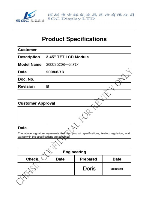
Product SpecificationsCustomerDescription 3.45” TFT LCD ModuleModel Name SGC035COM—54PINDate 2008/6/13Doc. No.Revision BCustomer ApprovalDateThe above signature represents that the product specifications, testing regulation, and warranty in the specifications are acceptedEngineeringCheck Date Prepared DateDoris2008/6/13CONTENTSNo. ITEM PAGE0 RECORD OF REVISION 31 SUMMARY 42 FEATURES 43 GENERAL SPECIFICATIONS 44 ABSOLUTE MAXIMUM RATINGS 45 ELECTRICAL CHARACTERISTICS 56 DC CHARATERISTICS 67 AC CHARACTERISTICS 6~108 OPTICAL CHARATERISTIC 119 TOUCH PANEL 14~1510 INTERFACE 16~1911 BLOCK DIAGRAM 2012 QUALITY ASSURANCE 2113 OUTLINE DRAWING 2214 PACKAGE INFORMATION 2315 PRECAUTIONS 24~26RECORD OF REVISIONSRevision Date Page DescriptionA 2008/2/12 all New CreationB 2008/6/13 18 LCM PIN Definition1. SUMMARYThis technical specification applies to 3.45“color TFT-LCD panel. The 3.45“ color TFT-LCD panel is designed for GPS, camcorder, digital camera application and other electronic products which require high quality flat panel displays. This module follows RoHS.2. FEATURESHigh Resolution: 230,400 Dots (320 RGB x 240). SGC 035COM—54PIN is atransmissive type color active matrix liquid crystal display (LCD) which uses amorphous thin film transistor (TFT) asswitching devices. This product is composed of a TFT LCD panel, driver ICs, FPC, backlight unit and touch panel.,3. GENERAL SPECIFICATIONSParameter Specifications Unit Screen size 3.45(Diagonal) InchDisplay Format 320 RGB x 240 DotActive area 70.08(H) x 52.56(V) mmDot size 73x 219 umPixel Configuration RGB-Stripe Outline dimension 76.9(W) x 63.9(H) x 3.3(D) mm Display Mode Normally white/Transmissive Surface Treatment Haze 20% Display Garmut NTSC 60% Input Interface Digital 24-bit RGB/SERIALRGB/CCIR656/CCIR601Weight (31) g View Angle direction 6 o’clockOperation -20~70 ℃Temperature RangeStorage -30~80 ℃4. ABSOLUTE MAXIMUM RATINGSItem Symbol Condition Min. Max. Unit Remark Power Voltage DVDD,AVDD GND=0 -0.3 5.0 V Input SignalVoltage V in GND=0 -0.3 VDD+0.3 VNOTE Logic OutputVoltageV OUT GND=0 -0.3 VDD+0.3 V NOTENote: Device is subject to be damaged permanently if stresses beyond those absolute maximum ratings listed above1. Temp. ≤ 60℃, 90% RH MAX.Temp. > 60℃, Absolute humidity shall be less than 90% RH at 60℃2.5. ELECTRICAL CHARACTERISTICS 5.1. Operating conditions:Parameter SymbolRatingMin. Typ. Max.Unit ConditionPower Voltage VCC 3.0 3.3 3.6 V Digital Operation CurrentIcc 8.6 mA Gate On Power VGH 14 15 18 V Gate Off Power VGL -11-10 -8V Vcom High Voltage VcomH 3.7 V Note1 Vcom low VoltageVcomL-1.6VNote1Vcom level max VcomA 6 VNote1. VcomH& VcomL :Adjust the color with gamma data. Vp-p should be higher then4V.(Option 5V)Note: Please power on following the sequence VCC Æ VDD5.2 LED driving conditionsParameter Symbol Min. Typ. Max. Unit Remark LED current- 20 - m A Power Consumption - 400 420 mW LED voltage VBL+ 18.619.8 21 V Note 1 LED Life Time - (50,000)- - HrNote 2,3Note 1 : There are 1 Groups LEDILEDNote 2 : Ta = 25℃Note 3 : Brightess to be decreased to 50% of the initial value深圳宏辉成液晶显示有限公司/6. DC CHARATERISTICSParameter SymbolRatingUnit Condition Min. Typ. Max.Low level input voltage V IL 0-0.3VCCVHight level input voltage V IH0.7VCC-VCC V7. AC CHARATERISTICSDigital Parallal RGB interfaceSignal Item Symbol Min Typ Max UnitFrequency Tosc - 156 - ns Dclk High Time Tch - 78 - nsLow Time Tcl - 78 - nsDataSetup Time Tsu 12 - - nsHold Time Thd 12 - - nsPeriod TH - 408 - Tosc Pulse Width THS 5 30 - ToscHsyncBack-Porch Thb 38 ToscDisplay Period TEP - 320 - ToscHsync-den time THE 36 68 88 TsocFront-Porch Thf - 20 - ToscPeriod Tv - 262 - THPulse Width Tvs 1 3 5 TH Vsync Back-Porch Tvb - 15 - TH Display Period Tvd - 240 - THFront-Porch Tvf 2 4 - TH1. Thp + Thb = 68, the user is make up by yourself.2. Tv = Tvs + Tvb + Tvd + Tvf , the user is make up by yourself.3.When SYNC mode is used,1st data start from 68th Dclk after Hsync fallingDigital Serial RGB interfaceSignal Item Symbol Min Typ Max Unit Frequency Tosc - 52 - ns Dclk High Time Tch - 78 - ns Low Time Tcl - 78 - nsData Setup Time Tsu 12 - - nsHold Time Thd 12 - - nsPeriod TH - 1224 - Tosc Pulse Width THS 5 90 - ToscHsyncBack-Porch Thb 114 ToscDisplay Period TEP - 960 - Tosc Hsync-den time THE 108 204 264Front-Porch Thf - 60 - ToscPeriod Tv - 262 - THPulse Width Tvs 1 3 5 THVsync Back-Porch Tvb - 15 - THDisplay Period Tvd - 240 - THFront-Porch Tvf 2 4 - TH Note: 1. Thp + Thb = 204, the user is make up by yourself.2. Tv = Tvs + Tvb + Tvd + Tvf , the user is make up by yourself.3. When SYNC mode is used,1st data start from 204th Dclk after Hsync fallinCCIR601/656 InterfaceSignalData Setup Time Tsu 12 - - ns Hold Time Thd 12 - - ns深圳宏辉成液晶显示有限公司/[_//f+--------------------H " "'= 1560--------------------+jInvalid Data Inva l i d Da t a018,0"'=DOTCLK In va li d DataIn v a l i d Data]---...t--f------------H018, =1440-------------+jslrL//RR[7:0]In va lid DataIn va l i d Dataf---- t.<sP = HBP[6:0]'4+STH[1:0'1-- *. - ----------- IH0,se = 128--- --- ----.!Figure1 CCIR601 Horizontal Timing深圳宏辉成液晶显示有限公司 /手机 : 133 166 766 58 MSN: lcd.sales@ QQ:1378107648Doc. No.SEL[2:0] = 100- 111, NTSCVSYNC HSYNCRR[7:0]tveP = VBP[6:0]DL1DL2DL3IDL2391DL240I---ODD Field VSYNCEVEN FieldHSYNCRR[7:0]tvsP= VBP[6:0] + 1·IODD FieldI IDL1DL2DL3IDL2391DL240ISEL[2:0] = 100- 111, PAL, PALM=OEVEN VSYNCHSYNCRR[7:0]tvsP= VBP[6:0]DL1DL2DL3IDL2791DL280IODD Field VSYNCEVEN Fi l eHSYNCRR[7:0]tvsP= VBP[6:0] + 1·IODD FieldI IDL1DL2DL3IDL2791DL280ISEL[2:0] = 100 - 111, PAL, PALM=1EVEN VSYNCHSYNCRR[7:0]tveP= VBP[6:0]DL1DL2DL3IDL2871DL288 1ODD Field VSYNCEVEN Fi l eHSYNCI深圳宏辉成液晶显示有限公司 /手机 : 133 166 766 58 MSN: lcd.sales@ QQ:1378107648IRR[7:0]lvsP= VBP[6 0] + 1·IDL1DL2DL3IDL287 1DL288 1Figure1CCIR601 Vertical Timing深圳宏辉成液晶显示有限公司 /手机 : 133 166 766 58 MSN: lcd.sales@ QQ:1378107648Figure2 CCIR656 Horizontal Timing深圳宏辉成液晶显示有限公司 /手机 : 133 166 766 58 MSN: lcd.sales@ QQ:1378107648Figure2 CCIR656 Vertical Timing深圳宏辉成液晶显示有限公司 /手机 : 133 166 766 58 MSN: lcd.sales@ QQ:1378107648Figure 3Digital RGB NTSC mode Vertical Data Format for 262THH cycle = 1224tHBP = 204HDISP = 960t HFP = 60DOTCLKHSYNCPixel DataDumm yD0D1----------D 957 D 958 D 959Dum mya ) Horizontal Data Transaction Tim ing V cycle = 262 Lines t VBP = 18VSYNC VDISP = 240 Lines t VFP = 4HSYNC Line 0 b ) Vertical Data Transaction Tim ing Line 239深圳宏辉成液晶显示有限公司 /手机 : 133 166 766 58 MSN: lcd.sales@ QQ:1378107648Figure 3 Data Transaction Timing in Serial RGB (8 bit) Interface (SYNC Mode)深圳宏辉成液晶显示有限公司 /手机 : 133 166 766 58 MSN: lcd.sales@ QQ:1378107648Figure3 Data Transaction Timing in Serial RGB (8 bit) Interface (DE Mode)深圳宏辉成液晶显示有限公司 /手机 : 133 166 766 58 MSN: lcd.sales@ QQ:1378107648Figure3Data Transaction Timing in Parallel RGB (24 bit) Interface (SYNC Mode)深圳宏辉成液晶显示有限公司 /手机 : 133 166 766 58 MSN: lcd.sales@ QQ:1378107648Figure4 Data Transaction Timing in Parallel RGB (24 bit) Interface (DE Mode)7.1.1 Standby ON/OFF Control LQ35NC211 has a power ON/OFF sequence control function. When STB pin is pulled L,blank data is outputted for 5-frames first, form the falling edge of the following VSYNC signal. The blank data would be gray level 255 for normally white LC.Figure5 Standby ON/OFF Control 7.1.2 Clock and Sync waveforms深圳宏辉成液晶显示有限公司 /手机 : 133 166 766 58 MSN: lcd.sales@ QQ:1378107648Figure6 CLK and IHS timing waveformTV FTC LTH B7.2 Reset Timing ChartThe RESET input must be held at least 1ms after power is stable8. OPTICAL CHARATERISTICTa=25±2℃, ILED=20mA Item Symbol Condition Min. Typ. Max. Unit Remark Response timeTr θ=0°、Φ=0°Tf- 10 ms- 15 msNote 3,5 Contrast ratio CRAt optimizedviewing angle300 400 - - Note 4,5 Color ChromaticityWhiteRedGreenBlueWxθ=0°、Φ=0WyRxθ=0°、Φ=0RyGxθ=0°、Φ=0GyBxθ=0°、Φ=0By(0.26) (0.31) (0.36) Note 2,6,7(0.28) (0.33) (0.38)Hor.ΘR(50) (60)Viewing angleΘL CR≧10(50) (60)Deg. Note 1Ver.ΦT(40) (50)ΦB(45) (55)Brightness - - 180 200 - cd/m2Center ofdisplayTa=25±2℃, I L=20mANote 1: Definition of viewing angle rangeFig. 8-1 Definition of viewing angleNote 2: Test equipment setup:After stabilizing and leaving the panel alone at a driven temperature for 10 minutes, the measurement should be executed. Measurement should be executed in a stable, windless, and dark room. Optical specifications are measured by Topcon BM-7 luminance meter 1.0° field of view at a distance of 50cm and normal direction.Fig. 8-2 Optical measurement system setupNote 3: Definition of Response time:The response time is defined as the LCD optical switching time interval between “White” state and“Black” state. Rise time, Tr, is the time between photo detector output intensity changed from 90﹪to 10﹪. And fall time, Tf, is the time between photo detector output intensity changedfrom10﹪to 90﹪.Note 4: Definition of contrast ratio:The contrast ratio is defined as the following expression.Contrast ratio (CR)= Luminance measured when LCD on the “White” stateLuminance measured when LCD on the “Black” stateNote 5: White Vi = V i50 ± 1.5VBlack Vi = Vi50 ± 2.0V“±” means that the analog input signal swings in phase with VCOM signal. “±” means that the analog input signal swings out of phase with VCOM signal.The 100% transmission is defined as the transmission of LCD panel when all the input terminals of module are electrically opened.Note 6: Definition of color chromaticity (CIE 1931)Color coordinates measured at the center point of LCDNote 7: Measured at the center area of the panel when all the input terminals of LCD panel are electrically opened.Brightness (min)Note 8 : Uniformity (U) = x 100%Brightness (max)9. TOUCH PANELNA10. INTERFACE10.1. LCM PIN DefinitionPin Symbol I/O Function Remark1 LED- I Backlight LED Ground2 LED- I Backlight LED Ground3 LED+ I Backlight LED Power4 LED+ I Backlight LED Power5 Y1 I Top electrode ,6 X1 I Right electrode7 NC Not Use8 /RESET - Hardware Reset9 SPENA I SPI Interface Data Enable Signal Note 310 SPCLK I SPI Interface Data Clock Note 311 SPDAT I SPI Interface Data Note 312 B0 I Blue Data Bit 013 B1 I Blue Data Bit 114 B2 I Blue Data Bit 215 B3 I Blue Data Bit 316 B4 I Blue Data Bit 417 B5 I Blue Data Bit 518 B6 I Blue Data Bit 619 B7 I Blue Data Bit 720 G0 I Green Data Bit021 G1 I Green Data Bit122 G2 I Green Data Bit223 G3 I Green Data Bit324 G4 I Green Data Bit425 G5 I Green Data Bit526 G6 I Green Data Bit627 G7 I Green Data Bit728 R0 I Red Data Bit0 /DX0 Note 429 R1 I Red Data Bit1 /DX1 Note 430 R2 I Red Data Bit2 /DX2 Note 431 R3 I Red Data Bit3 /DX3 Note 432 R4 I Red Data Bit4 /DX4 Note 4Control the input data format /floatingControl the input data formatControl the input data formatNot UseData Enable Input54 AVSS INote:1. The mode control (SEL2) not use ,it can’t control CCIR601 interface , If not use CCIR601 ,itcan floating.2. For digital RGB input data format, both SYNC mode and DE+SYNC mode are supported. If DEsignal is fixed low, SYNC mode is used. Otherwise, DE+SYNC mode is used.Suggest used SYNC mode!!Suggest the DE signal usually pull low.3. usually pull high.4. IF select serial RGB or CCIR601/656 input mode is selected,only DX0-DX7 used,and the other short to GND, Onlyselected serial RGB、CCIR601/656 interface,DX BUS will enable,Digital input mode DX0 is LSB and DX7 is MSB.5. Control the input data formatDoc. No.10.2 SPI timing CharacteristicsFigure8 SPI read、write timingFigure9 SPI timingFigure10 SPI Reference program10.3 SPI Register DescriptionWill be showing on Application Note From Chihsin .10.4 Basic Display Color and Gray ScaleColorRedMSB LSBInput Color DataGreenMSB LSBBlueMSBLSBR7 R6 R5 R4 R3 R2 R1 R0 G7 G6 G5 G4 G3 G2 G1 G0 B7 B6 B5 B4 B3 B2 B1 B0BasicColorsBlack Red(255) Green(255) Blue(255)CyanMagenta Yellow White 0 0 0 1 1 1 0 0 0 0 0 0 0 0 0 1 1 1 1 1 1 1 1 1 0 0 0 0 0 0 0 1 1 1 1 1 0 0 0 0 0 0 0 1 1 0 0 0 0 0 0 0 0 0 0 0 0 1 1 1 1 1 1 1 0 0 1 1 1 1 1 1 1 1 1 1 1 1 1 1 0 0 0 0 0 0 1 1 1 0 0 0 1 1 1 0 0 0 1 1 1 1 1 1 0 0 0 0 0 0 1 1 1 0 0 0 1 1 1 0 0 0 1 1 1 1 1 1 0 0 0 0 0 0 0 0 0 1 1 1 1 1 1 1 1 1 0 0 0 1 1 1 0 0 0 0 0 0 0 0 0 0 0 0 0 0 0 1 1 1 1 1 1 1 1 1 1 1 1 1 1 1 0 0 0 0 0 1 1 1 1 1RedRed(0) Dark Red(1) Red(2) :Red(253) Red(254)Red(255) Bright0 0 0 0 0 0 0 0 0 : : : 1 1 1 1 1 1 1 1 10 0 0 0 0 0 0 0 0 0 0 1 0 0 0 0 0 1 0 0 0 : : : : : : : 1 1 1 0 1 0 0 1 1 1 1 0 0 0 1 1 1 1 1 0 0 0 0 0 0 0 0 0 0 0 : : : 0 0 0 0 0 0 0 0 0 0 0 0 0 0 0 0 0 0 : : : 0 0 0 0 0 0 0 0 0 0 0 0 0 0 0 0 0 0 : : : 0 0 0 0 0 0 0 0 0 0 0 0 0 00 0 0 0 0 0 0 0 0 0 : : : : : 0 0 0 0 0 0 0 0 0 0 0 0 0 0 0GreenGreen(0) Dark 0 0 0 Green(1) 0 0 0 Green(2) 0 0 0:: : : Green(253) 0 0 0 Green(254) 0 0 0 Green(255)Bright 0 0 0 0 0 0 0 0 0 0 0 0 0 0 0 0 0 0 0 0 0 0 0 0 : : : : : : : 0 0 0 0 0 1 1 0 0 0 0 0 1 1 0 0 0 0 0 1 1 0 0 0 0 0 0 0 0 0 : : : 1 1 1 1 1 1 1 1 1 0 0 0 0 0 1 0 1 0 : : : 1 0 1 1 1 0 1 1 1 0 0 0 0 0 0 0 0 0 : : : 0 0 0 0 0 0 0 0 0 0 0 0 0 0 0 0 0 0 0 0 0 0 0 0 : : : : : 0 0 0 0 0 0 0 0 0 0 0 0 0 0 0Blue Blue(0) Dark Blue(1) Blue(2): Blue(253)Blue(254)Blue(255) Bright0 0 0 0 0 0 0 0 0 : : : 0 0 0 0 0 0 0 0 00 0 0 0 0 0 0 0 0 0 0 0 0 0 0 0 0 0 0 0 0 : : : : : : : 0 0 0 0 0 0 0 0 0 0 0 0 0 0 0 0 0 0 0 00 0 0 0 0 0 0 0 0 : : : 0 0 0 0 0 0 00 0 0 0 0 0 0 0 0 : : : 0 0 0 0 0 0 00 0 0 0 0 0 0 0 0 : : : 1 1 1 1 1 1 10 0 0 0 0 0 0 0 0 1 0 0 0 1 0 : : : : : 1 1 1 0 1 1 1 1 1 0 1 1 1 1 111. BLOCK DIAGRAMCUSTOMER’S SYSTEMDigital24-bits,CCIR656, CCIR601,SERIAL SPCLK, SPDAT, Hsync, Vsync, DCLK12. QUALITY ASSURANCENo. Test Items Test Condition REMARK 1 High Temperature Storage Test Ta=80℃ Dry 240h 2 Low Temperature Storage Test Ta=-30℃ Dry 240h 3 High Temperature Operation Test Ta=70℃ Dry 240h 4 Low Temperature Operation Test Ta=-20℃ Dry 240h5High Temperature and High HumidityOperation TestTa=60℃ 90%RH 240h6 Electro Static Discharge Test7 Shock Test (non-operating)8 Vibration Test (non-operating) Panel surface / top case. Contact / Air :±6KV / ±8KV ,150pF ,330ΩShock Level : 100GWaveform : Half Sinusoidal WaveShock Time : 6msNumber of Shocks : 3 times for each ±X, ±Y, ±Z direction Frequency range: 10Hz ~ 550HzStoke :1.3mmSweep : 1.5G, 33.3~400HzVibration : Sinusoidal Wave, 1Hrsfor X,YZ direction.Non-operating9 Thermal Shock Test-20℃(0.5h) ~ 70℃(0.5h) / 100cycles***** T a = Ambient TemperatureNote:1. The test samples have recovery time for 2 hours at room temperature before the function check. In the standard conditions, there is no display function NG issue occurred.2. All the cosmetic specifications are judged before the reliability stress.Doc. No.13. OUTLINE DRAWING Rev: BPage: 27 of 30Date: 2008/6/13ITO Film:Sheet Resistance 200~900ΩITO Glass:Sheet Resistance 200~900ΩSurface hardness MIN. 3H此區顯示為 lable 的貼附範圍lable 的實際大小則依據B L specComponent H=1.5mmX2 Y1Y2 X1 +Kapton1DATEDATEDATE 2007-11-192007-11-19TITLE:8Doc. No.14.PACKAGE INFORMATION Rev: BPage: 28 of 30Date: 2008/6/132APPROVED DATEE奇信電子股份有限公司DWG. NO.: HS-P-03450915QH011CHECKED DATE REV.:UNIT: SCALE:SHEET:DESIGNER Lake Chao DATE 01/15"07SIEZ: A2PART NO.: 09150190-001:1 1/14 5DRAWER Lake Chao7DATE 01/15"078TITLE:包材圖15 RECAUTIONSPlease pay attention to the following when you use this TFT LCD module.15.1 MOUNTING PRECAUTIONS(1) You must mount a module using arranged in four corners or four sides.(2) You should consider the mounting structure so that uneven force (ex. Twisted stress) is notapplied to the module.And the case on which a module is mounted should have sufficient strength so that external force is not transmitted directly to the module.(3) Please attach a transparent protective plate to the surface in order to protect the polarizer.Transparent protective plate should have sufficient strength in order to the resist external force.(4) You should adopt radiation structure to satisfy the temperature specification.(5) Acetic acid type and chlorine type materials for the cover case are not describe becausethe former generates corrosive gas of attacking the polarizer at high temperature and the latter causes circuit break by electro-chemical reaction.(6) Do not touch, push or rub the exposed polarizers with glass, tweezers or anything harderthan HB pencil lead. And please do not rub with dust clothes with chemical treatment.Do not touch the surface of polarizer for bare hand or greasy cloth. (Some cosmetics are determined to the polarizer)(7) When the surface becomes dusty, please wipe gently with adsorbent cotton or other softmaterials like chamois soaks with petroleum benzene. Normal-hexane is recommended for cleaning the adhesives used to attach front / rear polarizers. Do not use acetone, toluene and alcohol because they cause chemical damage to the polarizer.(8) Wipe off saliva or water drops as soon as possible. Their long time contact with polarizercauses deformations and color fading.(9) Do not open the case because inside circuits do not have sufficient strength.15.2 OPERATING PRECAUTIONS(1) The spike noise causes the mis-operation of circuits. It should be lower than followingvoltage:V=±200mV(Over and under shoot voltage)(2) Response time depends on the temperature. (In lower temperature, it becomes longer.)(3) Brightness depends on the temperature. (In lower temperature, it becomes lower)And in lower temperature, response time (required time that brightness is stable after turned on) becomes longer.(4) Be careful for condensation at sudden temperature change. Condensation makes damageto polarizer or electrical contacted parts. And after fading condensation, smear or spot will occur.(5) When fixed patterns are displayed for a long time, remnant image is likely to occur.(6) Module has high frequency circuits. Sufficient suppression to the electromagneticinterference shall be done by system manufacturers. Grounding and shielding methods may be important to minimize the interference.15.3 ELECTROSTATIC DISCHARGE CONTROLSince a module is composed of electronic circuits, it is not strong to electrostatic discharge.Make certain that treatment persons are connected to ground through wristband etc. And don’t touch interface pin directly.15.4 PRECAUTIONS FOR STRONG LIGHT EXPOSUREStrong light exposure causes degradation of polarizer and color filter.15.5 STORAGE When storing modules as spares for a long time, the following precautions are necessary. (1) Store them in a dark place. Do not expose the module to sunlight or fluorescent light. Keep the temperature between 5℃ and 35℃ at normal humidity. (2) The polarizer surface should not come in contact with any other object. It is recommended that they be stored in the container in which they were shipped. 15.6 HANDLING PRECAUTIONS FOR PROTECTION FILM (1) When the protection film is peeled off, static electricity is generated between the film and polarizer. This should be peeled off slowly and carefully by people who are electrically grounded and with well ion-blown equipment or in such a condition, etc. (2) The protection film is attached to the polarizer with a small amount of glue. Is apt to remain on the polarizer.Please carefully peel off the protection film without rubbing it against the polarizer. (3) When the module with protection film attached is stored for a long time, sometimes there remains a very small amount of glue still on the polarizer after the protection film is peeled off. (4) You can remove the glue easily. When the glue remains on the polarizer surface or its vestige is recognized, please wipe them off with absorbent cotton waste or other soft material like chamois soaked with normal-hexane. 15.7 Cautions for installing and assembling Bezel edge must be positioned in the area between the Active area and View area. The bezel may press the touch screen and cause activation if the edge touches the active area. A gap of approximately 0.5mm is needed between the bezel and the top electrode. It may cause unexpected activation if the gap is too narrow. There is a tolerance of 0.2 to 0.3mm for the outside dimensions of the touch panel and tail. A gap must be made to absorb the tolerance in the case and connector.。
NS4205深圳市纳芯威科技有限公司双声道D类音频功率放大器说明书
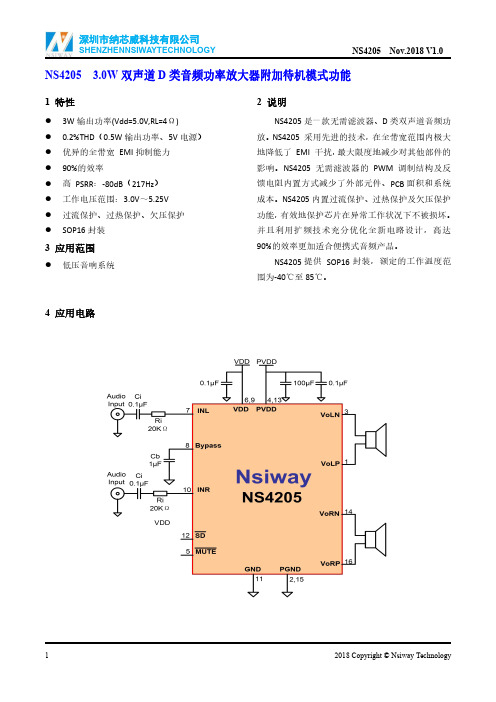
NS4205 3.0W双声道D类音频功率放大器附加待机模式功能1特性●3W输出功率(Vdd=5.0V,RL=4Ω)●0.2%THD(0.5W输出功率、5V电源)●优异的全带宽EMI抑制能力●90%的效率●高PSRR:-80dB(217Hz)●工作电压范围:3.0V~5.25V●过流保护、过热保护、欠压保护●SOP16封装3应用范围●低压音响系统2说明NS4205是一款无需滤波器、D类双声道音频功放。
NS4205采用先进的技术,在全带宽范围内极大地降低了EMI干扰,最大限度地减少对其他部件的影响。
NS4205无需滤波器的PWM调制结构及反馈电阻内置方式减少了外部元件、PCB面积和系统成本。
NS4205内置过流保护、过热保护及欠压保护功能,有效地保护芯片在异常工作状况下不被损坏。
并且利用扩频技术充分优化全新电路设计,高达90%的效率更加适合便携式音频产品。
NS4205提供SOP16封装,额定的工作温度范围为-40℃至85℃。
4应用电路5管脚配置NS4205SOP8的俯视图如下图所示:6极限工作参数●电源电压范围 2.8V~5.5V ●输入电压范围-0.3V~VDD ●ESD电压(HBM)4000V ●工作温度范围-40℃~+85℃●存储温度范围-65℃~+150℃●最大结温+150℃●焊接温度(10s内)+220℃●θJC)/θJA)(SOP-16)20/80o C/W 注:超过上述极限工作参数范围可能导致芯片永久性的损坏。
长时间暴露在上述任何极限条件下可能会影响芯片的可靠性和寿命。
7功能框图图3工作条件(除非特别说明):T A=25℃,V DD=5V。
注:测试D类时必须加低通滤波器,一般由33uH电感和1uF电容构成。
为减小功率损耗和干扰噪声,让测试数据更加精准,测试NS4205时可选用电阻电容做滤波器,电阻值选500Ω,电容值选10nF。
10典型特性曲线11应用说明11.1工作模式设置NS4205的工作模式通过管脚/SD 和/MUTE 设置,如下表。
ACX502BMU索尼3.5寸液晶屏
HT CC on f i d e n t i aHT CC on f i d e n t i aHT CC on f i d e n t i aHT CC on f i d e n t i aHT CC on f i d e n t i aHT CC on f i d e n t i aHT CC on f i d e n t i aHT CC on f i d e n t i aHT CC on f i d e n t i aHT CC on f i d e n t i aHT CC on f i d e n t i aHT CC on f i d e n t i aHT CC on f i d e n t i aHT CC on f i d e n t i aHT CC on f i d e n t i aHT CC on f i d e n t i aHT CC on f i d e n t i aHT CC on f i d e n t i aHT CC on f i d e n t i aHT CC on f i d e n t i aHT CC on f i d e n t i aHT CC on f i d e n t i aHT CC on f i d e n t i aHT CC on f i d e n t i aHT CC on f i d e n t i aHT CC on f i d e n t i aHT CC on f i d e n t i aHT CC on f i d e n t i aHT CC on f i d e n t i aACX502BMU-7LCD panel Light source 30•‹ Oscilloscope Optical detectorDisplay Data 100% 90% Optical Instruments ResponseWhite(111111) ToffBlack(000000)Ton10% 0%Fig.3 Measurement system-3100% 90%Relative Reflectivity50%10% 0%HT CV10Fig.4 V-R characteristics** Liquid crystal voltage = |Selected voltage level - Common voltage + Reference voltage center - Common voltage center | See page17 for ‘Selected voltage level ‘.CoV50 V90 Selected voltage level (V)31nfide nti aWhite(111111) TimeACX502BMU-7400•}50mm1 •KReflective LCD Module(a)The apparatus for Luminance measurementK K/6 K/3 K/3L/6 1 L/3 L 4 L/3 7 L/6 2Co5 6 8 9 Fig.5 Measurement system-432HT C(b)The spot locations for luminance measurementnfiK/6 3 FPCde nti aIlluminance Colorimeter BM-5AACX502BMU-7Amplifier (Rion NA-42)FFT (Rion SA-01A2)PCLCD10mm LCD module Wood plate Measurement SystemMeasurement pointFig.6 Measurement system-5HT CCo33nfide nti aMicrophone (Rion NH-34)ACX502BMU-721. Note on handling(1) Static charge prevention Be sure to take the following protective measures. TFT-LCD panels are easily damaged by static charges. A) Use non-chargeable gloves, or simply use bare hands. B) Use an earth-band when handling. C) Do not touch any electrodes of a panel. D) Wear non-chargeable clothes and conductive shoes. E) Install grounded conductive mats on the working floor and working table. F) Keep panels away from any charged materials. G) Use ionized air to discharge the panels. (2) Protection from dust and dirt A) Operate in a clean environment. B) Do not touch the front light surface. The surface is easily scratched . C) Use ionized air to blow dust off the panel.(3) Other handling precautions A) Do not twist or bend the flexible PC board especially at the connection region because the board is easily deformed. B) Do not drop the module. C) Do not twist or bend the module. D) Keep the module away from heat sources. E) Do not dampen the module with water or other solvents. F) Avoid storage or using the module at high temperatures or high humidity , as this may result in damage.HT CCo34nfide nti a。
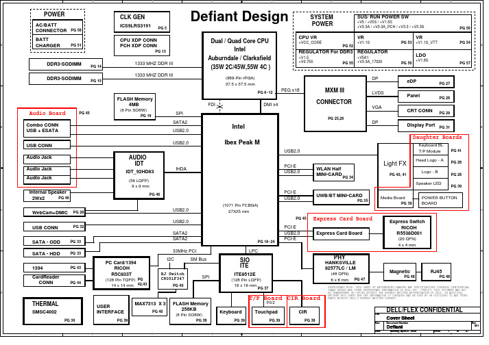
DELL外星人系列,15寸带独显电路图
27 28 29 30 31 32 33 34
C
V V V V V V V V
35 36 37 38 39 40,41
C
V
V
V
V
define define V V
define
V V
V V
define WOLdefine WOLdefine WOL
By Albert
D
D
PROPRIETARY NOTE: THIS SHEET OF ENGINEERING DRAWING AND SPECIFICATIONS CONTAINS CONFIDENTIAL TRADE SECRET AND OTHER PROPRIETARY INFORMATION OF DELL INC. ("DELL") THIS DOCUMENT MAY NOT BE TRANSFERRED OR COPIED WITHOUT THE EXPRESS WRITTEN AUTHORIZATION OF DELL. IN ADDITION, NEITHER THIS SHEET NOR THE INFORMATION IT CONTAINS MAY BE USED BY OR DISCLOSED TO ANY THIRD PARTY WITHOUT DELL'S EXPRESS WRITTEN CONSENT.
A
SA_CK0 SA_CK1
2 333MHz MAX 2
?MHz
BCLK_ITP BCLK_ITP#
SO-DIMM 1
PROPRIETARY NOTE: THIS SHEET OF ENGINEERING DRAWING AND SPECIFICATIONS CONTAINS ONFIDENTIAL TRADE SECRET AND OTHER PROPRIETARY INFORMATION OF DELL INC. ("DELL") THIS DOCUMENT MAY NOT BE TRANSFERRED OR COPIED WITHOUT THE EXPRESS WRITTEN AUTHORIZATION OF DELL. IN ADDITION, NEITHER THIS SHEET NOR THE INFORMATION IT CONTAINS MAY BE USED BY OR DISCLOSED TO ANY THIRD PARTY WITHOUT DELL'S EXPRESS WRITTEN CONSENT.
贴片电阻常见封装有9种(学)
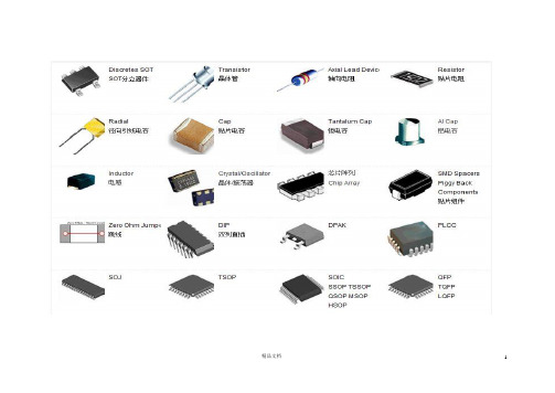
贴片电阻常见封装有9种,用两种尺寸代码来表示。
一种尺寸代码是由4位数字表示的EIA(美国电子工业协会)代码,前两位与后两位分别表示电阻的长与宽,以英寸为单位。
我们常说的0603封装就是指英制代码。
另一种是米制代码,也由4位数字表示,其单位为毫米。
下表列出贴片电阻封装英制和公制的关系及详细的尺寸:英制(inch)公制(mm)长(L)(mm)宽(W)(mm)高(t)(mm)a(mm)b(mm)020106030.60±0.050.30±0.050.23±0.050.10±0.050.15±0.05 04021005 1.00±0.100.50±0.100.30±0.100.20±0.100.25±0.10 06031608 1.60±0.150.80±0.150.40±0.100.30±0.200.30±0.20 08052012 2.00±0.201.25±0.150.50±0.100.40±0.200.40±0.20 12063216 3.20±0.201.60±0.150.55±0.100.50±0.200.50±0.20 12103225 3.20±0.202.50±0.200.55±0.100.50±0.200.50±0.20 18124832 4.50±0.203.20±0.200.55±0.100.50±0.200.50±0.20 20105025 5.00±0.202.50±0.200.55±0.100.60±0.200.60±0.20 25126432 6.40±0.203.20±0.200.55±0.100.60±0.200.60±0.20一、零件规格:(a)、零件规格即零件的外形尺寸,SMT发展至今,业界为方便作业,已经形成了一个标准零件系列,各家零件供货商皆是按这一标准制造。
U-SIN-R6000C-HRCN3 无纸记录仪 使用说明书
请将本手册交于操作者阅读。 在操作之前,请熟读本手册,并对产品有深入了解。 本手册只对产品的功能进行阐述,本公司不保证该产品将适合于用 户的某一特殊用途。
产品保护、安全及改造相关注意事项
为了确保安全使用本产品以及由其控制的系统,操作时请务必遵守 本手册中所述说明和注意事项。如果违反操作规程,则有可能会损坏本 产品所提供的保护功能。对由以上情况产生的质量、性能、功能和安全 问题,本公司不承担任何责任。
III
够完善,请勿运行。 仪表壳体上的通风孔须保持通畅,避免由于高温发生故障、动 作异常、寿命缩短和火灾。 请严格按照本手册的各项说明进行操作,否则可能损坏仪表的 保护装置。
开箱时若发现仪表损坏或变形,请勿使用。 安装时避免灰尘、线头、铁屑或其它异物进入仪表,否则会发 生动作异常或故障。 运行过程中,如需进行修改组态、信号输出、启动、停止等操 作,应充分考虑操作安全性,错误操作可能导致仪表和被控设备 发生故障乃至损坏。 仪表各部件有一定的寿命期限,为保证长期使用,务必进行定 期保养和维护。 报废本产品时,请按工业垃圾处理,避免污染环境。 不使用本产品时,请务必断开产品电源。 本仪表运行过程中如发现冒烟,异味,异响等异常情况时,请 立即关掉电源开关,同时切断供给电源,并及时与本公司取得联 系。
序号
产品包装内容
名称
数量
备注
1
无纸记录仪
1
2
说明书
1
3
合格证
1
V
目录 第一章 产品概述..............................................................................................1 第二章 主要技术参数......................................................................................1 第三章 使用注意事项及安装......................................................................... 3
额定参数——精选推荐
DWIN DMD64480A-01W 智能LCD显示终端Ver1.0 1额定参数! 供电电源:DC12-28V 8VA,纹波不超过100mVp-p;! 工作电流(供电电压为DC12V):650mA(背光开)/150mA(背光关);! 通信接口:3线制(DIN/DOUT/GND)RS232串行接口;! 背光方式:CCFL背光;! 显示颜色:256色;! LCD类型:640×4800点阵 10.4” TFT LCD! 西文字库:8×8、8×12点阵全ASCII字符;! 中文字库:12×12、16×16、24×24、32×32点阵全GB2312简体中文点阵字库;! 用户可配置FLASH空间:512KB字库空间,16MB图片存储空间;! 工作温度范围:-20℃-65℃2 软件接口2.1基本约定串口格式:UART(RS232),1/N、8、1、波特率可软件设置;帧结构:0xAA(帧头)+指令码(1字节,定义见接口指令集)+数据(N字节,N<253);帧结束标志:接收超时,超时定时器长度可软件设置。
2.2指令集说明:1.X(XH:XL),Y表示屏幕坐标,XH是X高字节,XL是X低字节;X范围0x00-0x27F,Y范围0x00-0x1DF。
2.所有指令均为十六进制(HEX)格式。
类型指令码数据说明无(下行)查询终端上电是否就绪,终端上电后到能够相应指令需要0.5-2秒时间,随电源不同而不同。
0x00‘OK’(上行)终端应答。
如果终端上电初始化过程未结束,将不应答。
握手举例:查询终端上电是否就绪串口下发: AA 00如果终端就绪,终端将应答:AA 00 4F 4B 04 07(生产日期)0x40 COLOR+BKCOLOR 设置当前调色板,BKCOLOR为背景颜色(比如清屏即是用背景色填充全屏),COLOR为前景颜色。
颜色范围为0x00-0xFF,最多256色。
W25X16
Publication Release Date: May 5, 200816M-BIT, 32M-BIT, AND 64M-BIT SERIAL FLASH MEMORY WITH4KB SECTORS AND DUAL OUTPUT SPITable of Contents1.GENERAL DESCRIPTION (4)2.FEATURES (4)3.PIN CONFIGURATION SOIC 150-MIL (5)4.PIN CONFIGURATION SOIC 208-MIL (5)5.PAD CONFIGURATION WSON 6X5-MM & 8X6-MM (5)6.PIN CONFIGURATION PDIP 300-MIL (6)7.PIN DESCRIPTION SOIC 150 / 208-MIL, PDIP 300-MIL, WSON 6X5 / 8X6-MM (6)8.PIN CONFIGURATION SOIC 300-MIL (7)9.PIN DESCRIPTION SOIC 300-MIL (7)9.1Package Types (8)9.2Chip Select (/CS) (8)9.3Serial Data Output (DO) (8)9.4Write Protect (/WP) (8)9.5HOLD (/HOLD) (8)9.6Serial Clock (CLK) (8)9.7Serial Data Input / Output (DIO) (8)10.BLOCK DIAGRAM (9)11.FUNCTIONAL DESCRIPTION (10)11.1SPI OPERATIONS (10)11.1.1SPI Modes (10)11.1.2Dual Output SPI (10)11.1.3Hold Function (10)11.2WRITE PROTECTION (11)11.2.1Write Protect Features (11)12.CONTROL AND STATUS REGISTERS (12)12.1STATUS REGISTER (12)12.1.1BUSY (12)12.1.2Write Enable Latch (WEL) (12)12.1.3Block Protect Bits (BP2, BP1, BP0) (12)12.1.4Top/Bottom Block Protect (TB) (12)12.1.5Reserved Bits (12)12.1.6Status Register Protect (SRP) (13)12.1.7Status Register Memory Protection (14)12.2INSTRUCTIONS (16)12.2.1Manufacturer and Device Identification (16)Publication Release Date: may 5, 200812.2.2 Instruction Set...............................................................................................................17 12.2.3 Write Enable (06h)........................................................................................................18 12.2.4 Write Disable (04h).......................................................................................................18 12.2.5 Read Status Register (05h)..........................................................................................19 12.2.6 Write Status Register (01h)..........................................................................................20 12.2.7 Read Data (03h)...........................................................................................................21 12.2.8 Fast Read (0Bh)...........................................................................................................22 12.2.9 Fast Read Dual Output (3Bh).......................................................................................23 12.2.10 Page Program (02h)...................................................................................................24 12.2.11 Sector Erase (20h).....................................................................................................25 12.2.12 Block Erase (D8h)......................................................................................................26 12.2.13 Chip Erase (C7h)........................................................................................................27 12.2.14 Power-down (B9h)......................................................................................................28 12.2.15 Release Power-down / Device ID (ABh).....................................................................29 12.2.16 Read Manufacturer / Device ID (90h).........................................................................31 12.2.17JEDEC ID (9Fh) (32)13. ELECTRICAL CHARACTERISTICS.........................................................................................33 13.1 Absolute Maximum Ratings..........................................................................................33 13.2 Operating Ranges.........................................................................................................33 13.3 Endurance and Data Retention....................................................................................34 13.4 Power-up Timing and Write Inhibit Threshold..............................................................34 13.5 DC Electrical Characteristics........................................................................................35 13.6 AC Measurement Conditions........................................................................................36 13.7 AC Electrical Characteristics........................................................................................37 13.8 Serial Output Timing.....................................................................................................39 13.9Input Timing (39)13.10 Hold Timing.................................................................................................................39 14.PACKAGE SPECIFICATION....................................................................................................40 14.1 8-Pin SOIC 150-mil (Package Code SN)......................................................................40 14.2 8-Pin SOIC 208-mil (Package Code SS)......................................................................41 14.3 8-Pin PDIP 300-mil (Package Code DA)......................................................................42 14.4 8-Contact 6x5mm WSON (Package Code ZP)............................................................43 14.5 8-Contact 8x6mm WSON (Package Code ZE)............................................................45 14.6 16-Pin SOIC 300-mil (Winbond Package Code SF).. (46)15. ORDERING INFORMATION ....................................................................................................47 16. REVISION HISTORY. (49)1.GENERAL DESCRIPTIONThe W25X16/W25X16A (16M-bit), W25X32 (32M-bit), and W25X64 (64M-bit) Serial Flash memories provide a storage solution for systems with limited space, pins and power. The 25X series offers flexibility and performance well beyond ordinary Serial Flash devices. They are ideal for code download applications as well as storing voice, text and data. The devices operate on a single 2.7V to 3.6V power supply with current consumption as low as 5mA active and 1µA for power-down. All devices are offered in space-saving packages.The W25X16/16A/32/64 array is organized into 8,192/16,384/32,768 programmable pages of 256-bytes each. Up to 256 bytes can be programmed at a time using the Page Program instruction. Pages can be erased in groups of 16 (sector erase), groups of 256 (block erase) or the entire chip (chip erase). The W25X16/16A/32/64 has 512/1024/2048 erasable sectors and 32/64/128 erasable blocks respectively. The small 4KB sectors allow for greater flexibility in applications that require data and parameter storage. (See figure 2.)The W25X16/16A/32/64 supports the standard Serial Peripheral Interface (SPI), and a high performance dual output SPI using four pins: Serial Clock, Chip Select, Serial Data I/O and Serial Data Out. SPI clock frequencies of up to 75MHz are supported allowing equivalent clock rates of 150MHz when using the Fast Read Dual Output instruction. These transfer rates are comparable to those of 8 and 16-bit Parallel Flash memories.A Hold pin, Write Protect pin and programmable write protect, with top or bottom array control features, provide further control flexibility. Additionally, the device supports JEDEC standard manufacturer and device identification.2.FEATURES•Family of Serial Flash Memories– W25X16/16A: 16M-bit/2M-byte (2,097,152) – W25X32: 32M-bit / 4M-byte (4,194,304)– W25X64: 64M-bit / 8M-byte (8,388,608)– 256-bytes per programmable page– Uniform 4K-byte Sectors / 64K-byte Blocks •SPI with Single or Dual Outputs– Clock, Chip Select, Data I/O, Data Out– Optional Hold function for SPI flexibility •Data Transfer up to 150M-bits / second– Clock operation to 75MHz– Fast Read Dual Output instruction– Auto-increment Read capability •Flexible Architecture with 4KB sectors– Sector Erase (4K-bytes)– Block Erase (64K-byte)– Page program up to 256 bytes <2ms– Minimum 100,000 erase/write cycles– 20-year retention •Low Power Consumption, Wide Temperature Range– Single 2.7 to 3.6V supply*– 5mA active current, 1µA Power-down (typ) – -40° to +85°C operating range •Software and Hardware Write Protection – Write-Protect all or portion of memory– Enable/Disable protection with /WP pin– Top or bottom array protection•Space Efficient Packaging– 8-pin SOIC 150-mil (X16A)– 8-pin SOIC 208-mil (X16/16A, X32)– 8-pin PDIP 300-mil (X16/16A, X32, X64) – 16-pin SOIC 300-mil (X16/16A, X32, X64) – 8-pad WSON 6x5-mm (X16/16A)– 8-pad WSON 8x6-mm (X32, X64)* Single 2.3V to 3.6V supply for W25X16ALPublication Release Date: May 5, 20083. PIN CONFIGURATION SOIC 150-MILFigure 1a. W25X16A Pin Assignments, 8-pin SOIC (Package Code SN)4. PIN CONFIGURATION SOIC 208-MILFigure 1b. W25X16/16A and W25X32 Pin Assignments, 8-pin SOIC (Package Code SS)5. PAD CONFIGURATION WSON 6X5-MM & 8X6-MMFigure 1c. W25X16/16A/32/64 Pad Assignments, 8-pad WSON 6x5-mm, 8x6-mm (Package Code ZP, ZE)6.PIN CONFIGURATION PDIP 300-MILFigure 1d. W25X16/16A, W25X32, W25X64 Pin Assignments, 8-pin PDIP (Package Code DA)7.PIN DESCRIPTION SOIC 150 / 208-MIL, PDIP 300-MIL, WSON 6X5 / 8X6-MMPIN NO. PIN NAME I/O FUNCTION1 /CS I Chip Select InputDataOutput2 DO O3 /WP I Write Protect Input4 GND Ground5 DIO I/O Data Input / Output6 CLK I Serial Clock Input7 /HOLD I HoldInputSupply8 VCC PowerPublication Release Date: may 5, 20088.PIN CONFIGURATION SOIC 300-MILFigure 1e. W25X16/16A, W25X32 and W25X64 Pin Assignments, 16-pin SOIC 300-mil (Package Code SF)9. PIN DESCRIPTION SOIC 300-MILPIN NO.PIN NAMEI/OFUNCTION1 /HOLD I Hold Input2 VCC Power Supply3 N/C No Connect4 N/C No Connect5 N/C No Connect6 N/C No Connect7 /CS I Chip Select Input8 DO O Data Output9 /WPIWrite Protect Input10 GND Ground 11 N/C No Connect 12 N/C No Connect 13 N/C No Connect 14 N/C No Connect 15 DIO I/O Data Input / Output 16CLKISerial Clock Input9.1Package TypesAt the time this datasheet was published not all package types had been finalized. Contact Winbond to confirm availability of these packages before designing to this specification. W25X16A is offered in an 8-pin plastic 150-mil width SOIC (package code SN). W25X16/16A and W25X32 are offered in an 8-pin plastic 208-mil width SOIC (package code SS). The W25X16/16A in 6x5-mm WSON (package code ZP) and 25X32 and 25X64 in 8x6-mm WSON (package code ZE). The 25X16/16A, W25X32 and W25X64 are offered in 16-pin plastic 300-mil width SOIC (package code SF) and 300-mil DIP (package code DA). See figures 1a-e.Package diagrams and dimensions are illustrated at the end of this datasheet.9.2Chip Select (/CS)The SPI Chip Select (/CS) pin enables and disables device operation. When /CS is high the device is deselected and the Serial Data Output (DO) pin is at high impedance. When deselected, the devices power consumption will be at standby levels unless an internal erase, program or status register cycle is in progress. When /CS is brought low the device will be selected, power consumption will increase to active levels and instructions can be written to and data read from the device. After power-up, /CS must transition from high to low before a new instruction will be accepted. The /CS input must track the VCC supply level at power-up (see “Write Protection” and figure 20). If needed a pull-up resister on /CS can be used to accomplish this.9.3Serial Data Output (DO)The SPI Serial Data Output (DO) pin provides a means for data and status to be serially read from (shifted out of) the device. Data is shifted out on the falling edge of the Serial Clock (CLK) input pin. 9.4Write Protect (/WP)The Write Protect (/WP) pin can be used to prevent the Status Register from being written. Used in conjunction with the Status Register’s Block Protect (BP2, BP1, and BP0) bits and Status Register Protect (SRP) bits, a portion or the entire memory array can be hardware protected. The /WP pin is active low.9.5HOLD (/HOLD)The /HOLD pin allows the device to be paused while it is actively selected. When /HOLD is brought low, while /CS is low, the DO pin will be at high impedance and signals on the DIO and CLK pins will be ignored (don’t care). When /HOLD is brought high, device operation can resume. The/HOLD function can be useful when multiple devices are sharing the same SPI signals. (“See Hold function”)9.6Serial Clock (CLK)The SPI Serial Clock Input (CLK) pin provides the timing for serial input and output operations. ("See SPI Operations")9.7Serial Data Input / Output (DIO)The SPI Serial Data Input/Output (DIO) pin provides a means for instructions, addresses and data to be serially written to (shifted into) the device. Data is latched on the rising edge of the Serial Clock (CLK) input pin. The DIO pin is also used as an output when the Fast Read Dual Output instruction is executed.10. BLOCK DIAGRAMPublication Release Date: may 5, 2008Figure 2. W25X16/16A, W25X32 and W25X64 Block Diagram11.FUNCTIONAL DESCRIPTION11.1SPI OPERATIONS11.1.1SPI ModesThe W25X16/16A/32/64 is accessed through an SPI compatible bus consisting of four signals: Serial Clock (CLK), Chip Select (/CS), Serial Data Input/Output (DIO) and Serial Data Output (DO). Both SPI bus operation Modes 0 (0,0) and 3 (1,1) are supported. The primary difference between Mode 0 and Mode 3 concerns the normal state of the CLK signal when the SPI bus master is in standby and data is not being transferred to the Serial Flash. For Mode 0 the CLK signal is normally low. For Mode 3 the CLK signal is normally high. In either case data input on the DIO pin is sampled on the rising edge of the CLK. Data on the DO and DIO pins are clocked out on the falling edge of CLK.11.1.2Dual Output SPIThe W25X16/16A/32/64 supports Dual output operation when using the "Fast Read with Dual Output" (3B hex) instruction. This feature allows data to be transferred from the Serial Flash memory at twice the rate possible with the standard SPI. This instruction is ideal for quickly downloading code from Flash to RAM upon power-up (code-shadowing) or for applications that cache code-segments to RAM for execution. The Dual output feature simply allows the SPI input pin to also serve as an output during this instruction. All other operations use the standard SPI interface with single output signal. 11.1.3Hold FunctionThe /HOLD signal allows the W25X16/16A/32/64 operation to be paused while it is actively selected (when /CS is low). The/HOLD function may be useful in cases where the SPI data and clock signals are shared with other devices. For example, consider if the page buffer was only partially written when a priority interrupt requires use of the SPI bus. In this case the/HOLD function can save the state of the instruction and the data in the buffer so programming can resume where it left off once the bus is available again.To initiate a/HOLD condition, the device must be selected with /CS low. A/HOLD condition will activate on the falling edge of the /HOLD signal if the CLK signal is already low. If the CLK is not already low the/HOLD condition will activate after the next falling edge of CLK. The/HOLD condition will terminate on the rising edge of the/HOLD signal if the CLK signal is already low. If the CLK is not already low the/HOLD condition will terminate after the next falling edge of CLK.During a/HOLD condition, the Serial Data Output (DO) is high impedance, and Serial Data Input/Output (DIO) and Serial Clock (CLK) are ignored. The Chip Select (/CS) signal should be kept active (low) for the full duration of the/HOLD operation to avoid resetting the internal logic state of the device.Publication Release Date: may 5, 200811.2 WRITE PROTECTIONApplications that use non-volatile memory must take into consideration the possibility of noise and other adverse system conditions that may compromise data integrity. To address this concern the W25X16/16A/32/64 provides several means to protect data from inadvertent writes.11.2.1 Write Protect Features • Device resets when VCC is below threshold. • Time delay write disable after Power-up. • Write enable/disable instructions.• Automatic write disable after program and erase. • Software write protection using Status Register.• Hardware write protection using Status Register and /WP pin. •Write Protection using Power-down instruction.Upon power-up or at power-down the W25X16/16A/32/64 will maintain a reset condition while VCC is below the threshold value of V WI , (See Power-up Timing and Voltage Levels and Figure 20). While reset, all operations are disabled and no instructions are recognized. During power-up and after the VCC voltage exceeds V WI , all program and erase related instructions are further disabled for a time delay of t PUW . This includes the Write Enable, Page Program, Sector Erase, Block Erase, Chip Erase and the Write Status Register instructions. Note that the chip select pin (/CS) must track the VCC supply level at power-up until the VCC-min level and t VSL time delay is reached. If needed a pull-up resister on /CS can be used to accomplish this.After power-up the device is automatically placed in a write-disabled state with the Status Register Write Enable Latch (WEL) set to a 0. A Write Enable instruction must be issued before a Page Program, Sector Erase, Chip Erase or Write Status Register instruction will be accepted. After completing a program, erase or write instruction the Write Enable Latch (WEL) is automatically cleared to a write-disabled state of 0.Software controlled write protection is facilitated using the Write Status Register instruction and setting the Status Register Protect (SRP) and Block Protect (TB, BP2, BP1, and BP0) bits. These Status Register bits allow a portion or all of the memory to be configured as read only. Used in conjunction with the Write Protect (/WP) pin, changes to the Status Register can be enabled or disabled under hardware control. See Status Register for further information.Additionally, the Power-down instruction offers an extra level of write protection as all instructions are ignored except for the Release Power-down instruction.12.CONTROL AND STATUS REGISTERSThe Read Status Register instruction can be used to provide status on the availability of the Flash memory array, if the device is write enabled or disabled, and the state of write protection. The Write Status Register instruction can be used to configure the devices write protection features. See Figure 3.12.1STATUS REGISTER12.1.1BUSYBUSY is a read only bit in the status register (S0) that is set to a 1 state when the device is executing a Page Program, Sector Erase, Block Erase, Chip Erase or Write Status Register instruction. During this time the device will ignore further instructions except for the Read Status Register instruction (see t W, t PP, t SE,t BE, and t CE in AC Characteristics). When the program, erase or write status register instruction has completed, the BUSY bit will be cleared to a 0 state indicating the device is ready for further instructions.12.1.2Write Enable Latch (WEL)Write Enable Latch (WEL) is a read only bit in the status register (S1) that is set to a 1 after executing a Write Enable Instruction. The WEL status bit is cleared to a 0 when the device is write disabled. A write disable state occurs upon power-up or after any of the following instructions: Write Disable, Page Program, Sector Erase, Block Erase, Chip Erase and Write Status Register.12.1.3Block Protect Bits (BP2, BP1, BP0)The Block Protect Bits (BP2, BP1, and BP0) are non-volatile read/write bits in the status register (S4, S3, and S2) that provide Write Protection control and status. Block Protect bits can be set using the Write Status Register Instruction (see t W in AC characteristics). All, none or a portion of the memory array can be protected from Program and Erase instructions (see Status Register Memory Protection table). The factory default setting for the Block Protection Bits is 0, none of the array protected. The Block Protect bits can not be written to if the Status Register Protect (SRP) bit is set to 1 and the Write Protect (/WP) pin is low.12.1.4Top/Bottom Block Protect (TB)The Top/Bottom bit (TB) controls if the Block Protect Bits (BP2, BP1, BP0) protect from the Top (TB=0) or the Bottom (TB=1) of the array as shown in the Status Register Memory Protection table. The TB bit is non-volatile and the factory default setting is TB=0. The TB bit can be set with the Write Status Register Instruction provided that the Write Enable instruction has been issued. The TB bit can not be written to if the Status Register Protect (SRP) bit is set to 1 and the Write Protect (/WP) pin is low.12.1.5Reserved BitsStatus register bit location S6 is reserved for future use. Current devices will read 0 for this bit location. It is recommended to mask out the reserved bit when testing the Status Register. Doing this will ensure compatibility with future devices.Publication Release Date: may 5, 200812.1.6 Status Register Protect (SRP)The Status Register Protect (SRP) bit is a non-volatile read/write bit in status register (S7) that can be used in conjunction with the Write Protect (/WP) pin to disable writes to status register. When the SRP bit is set to a 0 state (factory default) the /WP pin has no control over status register. When the SRP pin is set to a 1, the Write Status Register instruction is locked out while the /WP pin is low. When the/WP pin is high the Write Status Register instruction is allowed.Figure 3. Status Register Bit Locations12.1.7Status Register Memory ProtectionSTATUS REGISTER(1)W25X64 (64M-BIT) MEMORY PROTECTIONTB BP2 BP1 BP0 BLOCK(S) ADDRESSES DENSITY PORTION x 0 0 0 NONE NONE NONE NONE 0 0 0 1 126 and 127 7E0000h - 7FFFFFh 128KB Upper 1/640 0 1 0 124 and 127 7C0000h - 7FFFFFh 256KB Upper 1/320 0 1 1 120 thru 127 780000h - 7FFFFFh 512KB Upper 1/160 1 0 0 112 thru 127 700000h - 7FFFFFh 1MB Upper 1/80 1 0 1 96 thru 127 600000h - 7FFFFFh 2MB Upper 1/40 1 1 0 64 thru 127 400000h - 7FFFFFh 4MB Upper 1/21 0 0 1 0 and 1 000000h - 01FFFFh 128KB Lower 1/641 0 1 0 0 thru 3 000000h - 03FFFFh 256KB Lower 1/321 0 1 1 0 thru 7 000000h - 07FFFFh 512KB Lower 1/161 1 0 0 0 thru 15 000000h – 0FFFFFh 1MB Lower 1/81 1 0 1 0 thru 31 000000h – 1FFFFFh 2MB Lower 1/41 1 1 0 0 thru 63 000000h – 3FFFFFh 4MB Lower 1/2x 1 1 1 0 thru 127 000000h - 7FFFFFh 8MB ALLSTATUS REGISTER(1)W25X32 (32M-BIT) MEMORY PROTECTIONTB BP2 BP1 BP0 BLOCK(S) ADDRESSES DENSITY PORTION x 0 0 0 NONE NONE NONE NONE 0 0 0 1 63 3F0000h - 3FFFFFh 64KB Upper 1/640 0 1 0 62 and 63 3E0000h - 3FFFFFh 128KB Upper 1/320 0 1 1 60 thru 63 3C0000h - 3FFFFFh 256KB Upper 1/160 1 0 0 56 thru 63 380000h - 3FFFFFh 512KB Upper 1/80 1 0 1 48 thru 63 300000h - 3FFFFFh 1MB Upper 1/40 1 1 0 32 thru 63 200000h - 3FFFFFh 2MB Upper 1/21 0 0 1 0 000000h - 00FFFFh 64KB Lower 1/641 0 1 0 0 and 1 000000h - 01FFFFh 128KB Lower 1/321 0 1 1 0 thru 3 000000h - 03FFFFh 256KB Lower 1/161 1 0 0 0 thru 7 000000h - 07FFFFh 512KB Lower 1/81 1 0 1 0 thru 15 000000h – 0FFFFFh 1MB Lower 1/41 1 1 0 0 thru 31 000000h – 1FFFFFh 2MB Lower 1/2x 1 1 1 0 thru 63 000000h - 3FFFFFh 4MB ALLSTATUS REGISTER(1)W25X16/16A (16M-BIT) MEMORY PROTECTIONTB BP2 BP1 BP0 BLOCK(S) ADDRESSES DENSITY PORTION x 0 0 0 NONE NONE NONE NONE 0 0 0 1 31 1F0000h - 1FFFFFh 64KB Upper 1/320 0 1 0 30 and 31 1E0000h - 1FFFFFh 128KB Upper 1/160 0 1 1 28 thru 31 1C0000h - 1FFFFFh 256KB Upper 1/80 1 0 0 24 thru 31 180000h - 1FFFFFh 512KB Upper 1/40 1 0 1 16 thru 31 100000h - 1FFFFFh 1MB Upper 1/21 0 0 1 0 000000h - 00FFFFh 64KB Lower 1/321 0 1 0 0 and 1 000000h - 01FFFFh 128KB Lower 1/161 0 1 1 0 thru 3 000000h - 03FFFFh 256KB Lower 1/81 1 0 0 0 thru 7 000000h - 07FFFFh 512KB Lower 1/41 1 0 1 0 thru 15 000000h - 0FFFFFh 1MB Lower 1/2x 1 1 x 0 thru 31 000000h - 1FFFFFh 2MB ALL1. x = don’t carePublication Release Date: may 5, 200812.2INSTRUCTIONSThe instruction set of the W25X16/16A/32/64 consists of fifteen basic instructions that are fully controlled through the SPI bus (see Instruction Set table). Instructions are initiated with the falling edge of Chip Select (/CS). The first byte of data clocked into the DIO input provides the instruction code. Data on the DIO input is sampled on the rising edge of clock with most significant bit (MSB) first. Instructions vary in length from a single byte to several bytes and may be followed by address bytes, data bytes, dummy bytes (don’t care), and in some cases, a combination. Instructions are completed with the rising edge of edge /CS. Clock relative timing diagrams for each instruction are included in figures 4 through 19. All read instructions can be completed after any clocked bit. However, all instructions that Write, Program or Erase must complete on a byte boundary (CS driven high after a full 8-bits have been clocked) otherwise the instruction will be terminated. This feature further protects the device from inadvertent writes. Additionally, while the memory is being programmed or erased, or when the Status Register is being written, all instructions except for Read Status Register will be ignored until the program or erase cycle has completed.12.2.1Manufacturer and Device IdentificationMANUFACTURER ID (M7-M0)Winbond Serial Flash EFHDevice ID(ID7-ID0)(ID15-ID0)90h 9FhInstruction ABh,W25X16/16A 14h 3015hW25X32 15h 3016hW25X64 16h 3017hPublication Release Date: may 5, 200812.2.2 Instruction Set (1)INSTRUCTION NAMEBYTE 1 CODEBYTE 2 BYTE 3BYTE 4BYTE 5BYTE 6N-BYTES Write Enable 06h Write Disable 04hRead StatusRegister 05h (S7–S0)(1)(2)Write StatusRegister 01h S7–S0Read Data 03h A23–A16 A15–A8 A7–A0 (D7–D0) (Next byte) continuous Fast Read 0BhA23–A16A15–A8A7–A0dummy(D7–D0)(Next Byte) continuous Fast Read Dual Output 3Bh A23–A16 A15–A8 A7–A0 dummyI/O =(D6,D4,D2,D0)O =(D7,D5,D3,D1) (one byte per 4 clocks, continuous) Page Program02hA23–A16A15–A8A7–A0(D7–D0)(Next byte)Up to 256 bytes Block Erase(64KB)D8h A23–A16 A15–A8 A7–A0Sector Erase(4KB)20h A23–A16 A15–A8 A7–A0Chip Erase C7h Power-down B9hRelease Power-down / Device ID ABh dummy dummy dummy (ID7-ID0)(4)Manufacturer/Device ID (3)90h dummy dummy 00h (M7-M0) (ID7-ID0)JEDEC ID 9Fh(M7-M0)Manufacturer(ID15-ID8)Memory Type(ID7-ID0) CapacityNotes:1. Data bytes are shifted with Most Significant Bit first. Byte fields with data in parenthesis “( )” indicate data being read from the device on the DO pin.2. The Status Register contents will repeat continuously until /CS terminates the instruction.3. See Manufacturer and Device Identification table for Device ID information.4. The Device ID will repeat continuously until /CS terminates the instruction.12.2.3Write Enable (06h)The Write Enable instruction (Figure 4) sets the Write Enable Latch (WEL) bit in the Status Register to a 1. The WEL bit must be set prior to every Page Program, Sector Erase, Block Erase, Chip Erase and Write Status Register instruction. The Write Enable instruction is entered by driving /CS low, shifting the instruction code “06h” into the Data Input (DI) pin on the rising edge of CLK, and then driving /CS high.Figure 4. Write Enable Instruction Sequence Diagram12.2.4Write Disable (04h)The Write Dissable instruction (Figure 5) resets the Write Enable Latch (WEL) bit in the Status Register to a 0. The Write Disable instruction is entered by driving/CS low, shifting the instruction code “04h” into the DIO pin and then driving /CS high. Note that the WEL bit is automatically reset after Power-up and upon completion of the Write Status Register, Page Program, Sector Erase, Block Erase and Chip Erase instructions.Figure 5. Write Disable Instruction Sequence Diagram。
Pro-face 5.7英寸触摸屏操作器接口 PFXGP4301TADW 数据手册说明书
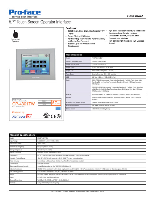
PFXGP4301TADWC
GP-4301TW: 5.7" TFT Color Touchscreen (Analog), QVGA, 2x Serial, Ethernet, 2x USB, 24VDC, UL/CE, Conformal Coating
Optional Items
Part Number
Connectivity
(WKHUQHW0XOWL/LQNIXQFWLRQ
0DVWHU
7KH(WKHUQHW0XOWL/LQNIXQFWLRQ DOORZV\RXWRHDVLO\DGGD*3DV DVXEGLVSOD\WRWKHIDFLOLW\ ZLWKRXWFKDQJLQJDQ\VHWWLQJVRI WKHFRQWUROGHYLFH
DC 24V QVGA
5.7-inch
Ethernet
Ro
Ethernet Backlight
Brightness and Contrast Controls Programming Memory Backup Memory
PFXGP4301TADW
320 x 240 pixels (QVGA) TFT Color LCD (5.7 inch) 65,536 Colors (no blink), 16,384 (blink) W115.2 x H86.4 mm [W4.54 x H3.40 in.] Resistive film analog 1024 x 1024 resolution USB Type-A (2.0) x 1 , USB mini-B (2.0) x1 COM1: RS-232C Asynchronous Transmission Data Length: 7 or 8 bits, Parity: None, Odd or Even, Stop Bit: 1 or 2 bits, Data Transmission Speed: 2,400 bps to 115.2 kbps, Connector: D-Sub9 (plug)
w25q16数据手册_引脚图_参数

8.
QUAD ENABLE (QE) – VOLATILE/NON-VOLATILE WRITABLE .............................................. 14
Write Protect Selection (WPS) – Volatile/Non-Volatile Writable ........................................15
4.3 Write Protect (/WP)............................................................................................................... 7
4.4 HOLD (/HOLD) ..................................................................................................................... 7
6.1 Standard SPI Instructions..................................................................................................... 9
6.2 Dual SPI Instructions ............................................................................................................ 9
Write Enable Latch (WEL) – Status Only...........................................................................11
3.5寸液晶屏SGC035G6-54NT

深圳市宏辉成科技有限公司Shenzhen SGC Techno logy Co, LtdSPECIFI CA TIONFORLCD M OD ULE手机:133 166 766 58 邮箱:lcd.sales@Customer:Product Model:Sample code:The specification of “TBD” should refer to the measured value of sample . If there is difference between the design specification and measured value, we naturally shall negotiate and agree to solution with customer.手机: 邮件:!P S(o zmShenzhen SGC Techno logy Co LtdRevision HistorvVers i on Contents Date NoteA Original2010.01.06Shenzhen SGC Techno logy Co, LtdContents©All Rights Reserved3/26REV.AShenzhen SGC Techno logy Co, Ltd1 Numbering System(1)(2) (3) (4)(5) (6) (7) 8NoDefinitionSpecifications(1)TFT LCMProductor No.KD ---- Wintektion technologiy Co.,Ltd(2)Display monitor opposite angle line sizeUnit :mm or mmm (size <10 inch: takes two integers ; size >=10 inch: takes three integers )(3)Productor TypesD ---- Digital photo frame / DVD G ----GPS M ----MPP ----Mobil-Phone(4)Productor Development Series No.By two figures characters expression from 01 to99(5)Interface PIN NumberBy two figures characters expression from 01 to99(6)With Touch Panel Or NotT----With T/PN----Without T/P(7)LCD TypeA----AUO M----CMO C----CPT P----PVI L----LG W----Wintek H----HSD T----T opply Y----Hydis I----Hitach S----Sharp(8)Productor Development edition No.By The English litters : A 1~ Z9©All Rights Reserved5/26REV.AShenzhen SGC Techno logy Co, Ltd2 ScopeThis specification applies to the TFT LCD module which is designed and manufactured by LCM Factory of Shenzhen Wintektion Technology Co.,Ltd.It is capable of using 262k colors mode 24bit parallel bi-directional interface.3 Normative ReferenceGB/T4619-1996Liquid Crystal Display Test MethodGB/T2424 Basic environmental Testing Procedures for Electric and Electronic Products.GB/T2423 Basic Testing Procedures for Electric and Electronic Products IEC61747-1 SIXTH PARTGB2828`2829-87 National Standard of PRC4 Definitions4.1 Definitions of VopThe definitions of threshold voltage Vth1, Vth2 the following typical waveforms are applied on liquid crystal by the method of equalized voltage for each duty and bias.selected waveform non-selected waveformVth1: The voltage which the brightness of segment indicates 50% ofsaturated value on the conditions of selected waveform(f f =80Hz, =10 =270 at 25 )Vth2: The voltage which the brightness of segment indicates 50% ofsaturated value on the conditions of non-selected waveform(f f =80Hz, =10 =270 at 25 )Vop: (Vth1(50%)+Vth2(50%))/2(f f =80Hz,=10=270 at 25 )4.2 Definition of Response Time Tr, TdTr: The time required which the brightness of segment becomes 10% from 100% when waveform is switched to selected one from non-selected one. (f f =80Hz, Φ=10°θ=270°at 25 )Shenzhen SGC Techno logy Co, Ltd Td: The time required which the brightness of segment©All Rights Reserved7/26REV.AShenzhen SGC Techno logy Co, Ltdbecomes 90% from 10% when waveform is switched to selected one from selected one. (f f =80Hz, Φ=10°θ=270°at 25 )4.3 Definition of Contrast Ratio CrCr=A/BA: Segments brightness in case of non-selected waveform B: Segments brightness in case of selected waveform4.4 Definition of Angle and Viewing RangeAngular Graph: Constrast RatioSuch as:Viewing Angle Range:80(Cr>2) Horizontal 70(Cr>2) Vertical5 Technology Specifications5.1 FeatureShenzhen SGC Techno logy Co, Ltd This single-display module is suitable for use in Multidedia Player products.Shenzhen SGC Techno logy Co, LtdThe LCD adopts one backlight with High brightness 6-lamps white LED.1) Construction: 3.5 color TFT-LCD ,White LED backlight, FPC.2) LCD:2.1 Amorphous-TFT3.5-inch display, transmissive, normally white type.2.2 320(RGB) 240dots Matrix.2.3 Narrow-contact ledge technique.2.4 LCD Driver IC: NT39016D 1.3) Low cross talk by frame rate modulation.4) 262K Color ,24bit RGB interface.5) Video signal interface: Parallel RGB .5.2 Mechanical SpecificationsItem SpecificationsUnit Dimensional outline 76.9(W) ×63.9(H)×3.2 (T) mm TP outline mmTP(V.A)mmTP(A.A)mmActive area 70.08(W) ×52.56 (H) mmPixel size 219(W) ×219(H) umResolution 320(RGB) 240 pixel 5.3 Absolute Max. Rating©All Rights Reserved9/26REV.AShenzhen SGC Techno logy Co, Ltd5.4 Electrical CharacteristicsDC Electr i cal Charact e r isticsD CE l ec t r ica l C h arac t e ri s t i cs Vt:TeslCond i tíon:VDIÞVDDP=3.3V I VDD A:51GN O:GNO A::GND P:0T A 25t) r cuígít a l cì(Fo r lhe dìFe thol V F8 0.55 .6 O. V O CiU C op.V ωrren 20mAβj5 Shenzhen SGC Techno logy Co Ltd5.5 Optical specificationsn e opUC3l Ch;l mctensocs sho berrasureo m d3ft( room A 1t er 5 mmutes o ef30αthe oP1J cal propo""ÐS aro f Y asurod 3t 00or poont of LCD scn:>o n _ AII np t 'ITI onals LCD par I mustbe g n._nd when me aMSTlf1g e center area of the paneLPh o O tectorF cldTFT -L CO Mod ule τhc cc:nte>" of tt C 3crccnCon a 5t Ra tioLum nan<::e C h lO maUCUY t .um U nlT onmty R esoαls e "P rr Pho1.0 d et< ::to r S R -3A B M-7ANote 2" oe nitionof Ni ng ar Ie r:a nge :m d meas -e rr sy mviow íng ang n asurod 31 tt C r po.n t of ttlo LCD by CC OSCOPE( 90--80)φ-00" 1:?_ o -dock dlfect n=180φ=o / > I7-""7'" τC ;1";T - q =270.;:) o'clock dlred íonF Ig 1 Definition of931E@AI I Rights Reserved 9/6 REV AShenzhen SGC Techno logy Co, Ltd5.6 LED back light specification (6 White Chips)Item Symbol Condition Min Typ Max Unit Forward Voltage Vf lf=20mA - 19.2 - V Uniformity (with L/G) B p lf=20mA 80 - - % Luminance for LCD L V If=20mA3600-cd/m2 LED CIRCUITShenzhen SGC Techno logy Co, LtdKDOS5G6-5 T-Al5.71nterface Pin Connections@A I/RightsRes ved11126REV.AShenzhen SGC Techno logy Co, Ltd6 Signal timing diagram and Circuit block diagram6.1 Circuit block diagram6.2 SignalTiming Diagram6.2.1Power ON SequenceP owerO n f SeqL nce03 6-54N T-AlTo p r even t I C frω1)power reset fa l lhe r lsl IImeσ01dlglal power supply V DD.s h ou l:l be n trol lV h n t he spec iFl ca tio o. fe r10the"A C Cha raa eris t1c l.o r the de II t im.eas e'00VD D PST n\'i rt t1)V Il IlVDDV IlIl PS T O (.h!..".."" )-l f \JV D D@AII Rights Reserved1Y26REV.At7f 深圳市宏辉成科技有限公司Shenzhen SGC Techno logy Co, LtdW'INT lC l r N Ei6.2.2Ser i a l mode t imi ng &c l ockKD036G6-6T-Al 3.Wir e T im i n g D i a g r a mV SDv - S N3I ! ul _---- f ' s A Y αC 1m 3 i s 1 !\ 1 l ! .\ I i I \ l r " \_J...-\J JT6.2.3 Se r i a l T r a n sm i ss i o n mode3-W ìr e Se r ìa l P ort Int erface (D efau l t R eglste r M ap)3.W i r e Cornmand F o rmalNT30016 s I h o 3-w l o 50 I tas m nu1afion lotfaeo lor aJ Itlo ωc lion am or$01.3.W i ro mmu C i ωn be lJi.ároc t øl ßl co troll t7f 100 "rwr b In I(I9SS i Nη9016 :J W . ire gn lJlnaωDS a "S l svo l11Cld o'for aB tho timo . and Wi ll nOI $Uoa nyωmmand 10 tho 3-Wio bus its ! Und read modo 3-W ìro I wi B flI tum lhe dat íl d un lS O" rolur llGd dala $uld b & 1 al tho r is 001 SPCK tornal ωntronor . O ata 1n Ih9 i.Z 13$0'w l bQ nor ω b'f 3-W @ no durlng writo oporation . a nd sho d bQ ignor r i ng rωd o ration $0.Ouring road opor a: \IlX t mal ntr I ÐrUkI tSPDA pinunc r -Hi.Z ph il!l o" aln &9". 10 thosoction 01-3-'11110 nmlng agram" l or tho d aU l .50Ad d fllSS {S :O ] Oa :0]SPEN8SPDASK1 ν'26 @AII Rights Reserved REV.A aTV::::fI C l K V : .. .- _L LL JL_JI_ m----L JL_ L l "wawy610N 3-Wlre Command rma :l 11 \ 03 6-54N T-Al6.2.3D EM ode T imingVe r t ica l T i m ing Oi ag r a "(DE M o de)A\\ . '!?" _..... J ?U L F . .. ......._... -ι•!>J;. -- .. --@- J _d ...'+;. :!1lE ......"" .h l-ru--l---y- 7-深圳市宏辉成科技有限公司Shenzhen SGC Techno logy Co, Ltd7 Initial code880 /-30 120hrs70 /-20 120hrs (operating60 ,90% RH, 96Hrs-30 (30Min ) 25 (5Min)80 (30Min)(conversion time, : 5 sec ) 20©All Rights Reserved17/26REV.A深圳市宏辉成科技有限公司Shenzhen SGC Techno logy Co, Ltd150 ( according to die if exist)Free faller movement for eachside cording angle (75cmHigh 6 sides 2 angle 210. Inspection standardD 0.10.1 D 0.15D 0.151 ν'26@AII Rights Reserved REV.A©All Rights Reserved 19/26 REV.AD 0.1 0.1 D 0.15 0.15 D 0.20 D 0.20 0.015 L 2.0 0.015 W1.0 0.025 WD 0.05 xC-STN : if D 0.1 , unqualified0.015 1.00.015 W 2.01.00.025 WD 0.050.015 , unqualified深圳市宏辉成科技有限公司Shenzhen SGC Techno logy Co, LtdComponentLeak Solder©All Rights Reserved21/26REV.A深圳市宏辉成科技有限公司Shenzhen SGC Techno logy Co, Ltd1/3 of solder side ofcomponent, reject1 Rolling strake with visual inspection,forbid2 Differentness of color in viewing areawith visual inspection ( full white redgreen blue), forbidDisplayinspection , forbid1 ν'26@AII Rights Reserved REV.AColor Of 10 CIECoordinatex ywhite±0.05 ±0.05 Red±0.05±0.05Green ±0.05 ±0.05Blue ±0.05 ±0.05 According to the specification or sample customer have approvedDrive LCD under normalcondition, 25 Φ =0 θ =0Test white red green blue with DMS Record11 BrightnessIn accord with product specificationDrive condition is according to specificationMeasure location is in Follow Picture3 Adjust brightness instrument tozero , burrow against the surface of LCD , press “measure” , record when the display is steady.(YOKOGAWA-3298)12CR (Max)According to specification Measure locationAccording to product specification Measure instrument ( DMS-501 )13Response time According to specification According to product specification Measure instrument ( DMS-501 )14Viewing angleVibration15 RingFrequency 16 Of FPC Bend According to specificationCompare with thesample customer supply According to the use of product( main FPC offoldaway cellphone 6thousand )According to product specification Measure instrument ( DMS-501 )Compare with the sample customer supply when assemble Measure instrument Bend angle : 150° Fix FPC in the casement when customer supply。
LQ035NC111
Page: 6 of 28
VGL -11 -10 -8
V
Vcom High Voltage VcomH
3.7
V
Note1
Vcom low Voltage VcomL
-1.6
V
Note1
Vcom level max
VcomA
6
V
Note1. VcomH& VcomL:Adjust the color with gamma data. Vp-p should be higher then
CONTENTS
No.
ITEM
0
RECORD OF REVISION
1
SUMMARY
2
FEATURES
3
GENERAL SPECIFICATIONS
4
ABSOLUTE MAXIMUM RATINGS
5
ELECTRICAL CHARACTERISTICS
6
DC CHARATERISTICS
7
AC CHARACTERISTICS
2. FEATURES High Resolution: 230,400 Dots (320 RGB x 240). LQ035NC111 is a transmissive type color active matrix liquid crystal display (LCD) which uses amorphous thin film transistor (TFT) as switching devices. This product is composed of a TFT LCD panel, driver ICs, FPC and a backlight unit.
华邦(winbond)产品手册
PRODUCT GUIDE ==Winbond、ISSI 授权香港及中国代理== 8 位单片宽工作电压系列
型号 ROM 型式 ROM RAM I/O 脚 外扩存储 器空间 64K 工作电压 定时器/ 计数器 3 封装 Int 特殊功能 PDIP 6 CMOS 通用功能 特殊 I/O 口 /INT2, /INT3,WDT 特殊 I/O 口 /INT2, /INT3,WDT 16 KB 掩膜 ROM W78L54 掩膜 16K 256 32/36 64K 5.5V - 1.8V 3 8 特殊 I/O 口 /INT2,/INT3,WDT W78L801 掩膜 4K 256 36 64K 5.5V - 1.8V 2 12 特殊 I/O 口,P1 口 退出省电方式 WDT 可多次编程,特殊 I/O 口 / INT2, /INT3, WDT 可多次编程特殊 I/O 口 / INT2, /INT3, WDT 可多次编程特殊 I/O 口 / INT2, /INT3, WDT 可多次编程,可在线编程 特殊 I/O 口/ INT2, /INT3 可多次编程,可在线编程 W78LE516 Flash EPROM 64K 512 32/36 64K 5.5V - 2.4V 3 8 特殊 I/O 口,/ INT2, /INT3, 可多次编程,可在线编程 W78LE365 Flash EPROM 64K 1280 32/36 64 K 5.5V - 2.4V 3 8 特殊 I/O 口/ INT2, /INT3,WTD,PWM 特殊 I/O 口 W78LE812 Flash EPROM 8K 256 36 64K 5.5V - 2.4V 3 14 P1 口退出省电方式 WDT,UART 40 44 44 40 44 44 40 44 44 40 44 44 40 44 44 40 PLCC 44 PQFP 44
MJD350 300V PNP高电压传输器TO252(DPAK)商品说明书
Features∙ BV CEO > -300V∙ I C = -0.5A Continuous Collector Current ∙ I CM = -0.75A Peak Pulse Current∙ Ideal for Power Switching or Amplification Applications ∙ Complementary NPN Type: MJD340∙ Totally Lead-Free & Fully RoHS Compliant (Notes 1 & 2) ∙ Halogen and Antimony Free. “Green” Device (Note 3) ∙ Qualified to AEC-Q101 Standards for High ReliabilityMechanical Data∙ Case: TO252 (DPAK)∙ Case Material: Molded Plastic, "Green" Molding Compound UL Flammability Classification Rating 94V-0 ∙ Moisture Sensitivity: Level 1 per J-STD-020∙ Terminals: Finish – Matte Tin Plated Leads, Solderable per MIL-STD-202, Method 208 ∙Weight: 0.34 grams (Approximate)Ordering Information (Note 4)Notes: 1. No purposely added lead. Fully EU Directive 2002/95/EC (RoHS), 2011/65/EU (RoHS 2) & 2015/863/EU (RoHS 3) compliant.2. See https:///quality/lead-free/ for more information about Diodes Incorporated’s definitions of Hal ogen- and Antimony-free, "Green" and Lead-free.3. Halogen and Antimony free "Green” products are defined as those which contain <900ppm bromine, <900ppm chlorine (<1500ppm tot al Br + Cl) and <1000ppm antimony compounds.4. For packaging details, go to our website at https:///design/support/packaging/diodes-packaging/.Marking InformationTop ViewDevice SchematicPin Out ConfigurationTop ViewMJD350 = Product Type Marking Code = Manufacturers’ Code Marking YYWW = Date Code MarkingYY = Last Two Digits of Year (ex: 18 = 2018) WW = Week Code (01 to 53)TO252 (DPAK)TO252 (DPAK)MJD350Thermal Characteristics(@T A = +25°C, unless otherwise specified.)Notes: 5. For a device mounted on FR-4 PCB with minimum recommended pad layout.6. Refer to JEDEC specification JESD22-A114 and JESD22-A115.Thermal Characteristics and Derating InformationElectrical Characteristics(@T A = +25°C, unless otherwise specified.)Note: 7. Measured under pulsed conditions. Pulse width ≤300μs. Duty cycle ≤2%.Typical Electrical Characteristics(@T A = +25°C, unless otherwise specified.)Package Outline DimensionsPlease see /package-outlines.html for the latest version.TO252 (DPAK)Suggested Pad LayoutPlease see /package-outlines.html for the latest version.TO252 (DPAK)Note:For high voltage applications, the appropriate industry sector guidelines should be considered with regards to creepage and clearance distances between device Terminals and PCB tracking.7°±1°Seating Plane。
Hi3798C V200
基本信息
文档版本 发布日期
00B02 2016-02-03
版权所有 © 深圳市海思半导体有限公司 2016。保留一切权利。
非经本公司书面许可,任何单位和个人不得擅自摘抄、复制本文档内容的部分或思商标均为深圳市海思半导体有限公司的商标。
3 启动模式.......................................................................................................................................3-1
4 地址空间映射...............................................................................................................................4-1
版本 00B01 00B02
修订说明 第一次临时版本发布。 修改地址空间映射。
文档版本 00B02 (2016-02-03)
海思专有和保密信息 版权所有 © 深圳市海思半导体有限公司
1-1
Hi3798C V200 Data Sheet 基本信息
目录
目录
前 言...............................................................................................................................................1-1
产品版本
与本文档相对应的产品版本如下。
诺瓦科技LED显示屏接收卡A5s规格书

1
接收卡 A5s 规格书
请勿擅自维修产品,您可以随时联系诺瓦科技。 请使用诺瓦科技的同款产品进行备件更换。
1 安全说明
西安诺瓦电子科技有限公司
2
接收卡 A5s 规格书
2 概述
2 概述
司
A5s 是诺瓦推出的小尺寸全功能高端接收卡,单卡带载 320×256(PWM IC)像素。
3.2 提升可维护性 .............................................................................................................................................. 4
司 1.2 安装和使用安全 ........................................................................................................................................... 1 公 2 概述..................................................................................................................................3
V1.0.1 V1.0.0
2017-07-27 2016-10-25
优化文档的内容及架构。
有限 第一次正式发布。
技
科
子
电
瓦
诺
安
西
ii
接收卡 A5s 规格书
执法终端、移动执法箱技术规格参数:

执法终端、移动执法箱技术规格参数:一、执法终端(含数据服务)34套,技术规格参数:1、执法终端:国内知名品牌,6寸屏,八核处理器,1600万像素,双卡双4G,安全操作系统,兼容android6.0,3G运行内存,32G机身内存,支持128G扩展内存。
2、数据服务:3年数据服务,每月国内语音通话500分钟,定向免费通话500分钟,国内流量1GB,定向流量2G。
二、移动执法箱2套,技术规格参数:1、笔记本电脑:操作系统:预装WIN8;CPU:INTEL酷睿I5-5200U,2.2GHz;三级缓存:3MB;内存:4GB DDR3L1600MHz;硬盘:8GB(SSD)+500GB(普通);屏幕:14英寸16:91366×768,LED背光防眩光屏;全屏触摸;显卡:Geforce830M;显存:2GB DDR3;多媒体:集成摄像头,内置音效芯片、扬声器、麦克风;网络:1000M以太网卡、4G无线网卡、蓝牙4.0;I/0接口:3×USB3.0、HDMI、耳机/麦克风、多合一读卡器;输入设备:触摸板+全尺寸键盘。
2、便携式打印机:最高分辨率不低于:4800×1200dpi;打印速度:黑白22ppm,彩色18ppm;最大打印幅面:A4便携式喷墨;支持USB2.0接口;进纸盒容量:不低于50页;标配蓝牙,锂电池。
3、数码摄像机:有效像素≥220万像素;数码变焦倍数:350倍;支持夜间拍摄与投影;光学变焦:30倍;传感器类型CMOS传感器,背照式Exmor R CMOS;影像处理器:BIONZ X存储:32G卡;动态有效像素:200万像素(16:9),150万像素(4:3);高清规格:1080p,扩展变焦:延伸光学变焦不低于55倍;光圈范围:F1.8-F4.0;支持光学防抖功能,OSS防抖;录制格式:图片:JPEG视频:AVCHD,MPEG-2,MP4;电池:标配锂电池。
4、单反相机:传感器类型:CMOS;传感器尺寸:22.3×14.9mm;总像素:不低于1850万像素;有效像素:1750万素;最高分辨率:5184×3456高清摄像:全高清(1080p)★影像处理系统:DIGIC5;支持夜间拍摄,自带闪光灯同步闪光速度不高于1/200秒;连拍:支持连拍功能,每秒不低于5张;光学防抖;存储:16G SD卡,读写速度大于30M/s;镜头描述:伸缩式套机镜头:EF-S18-55mm IS STM;最大光圈:F3.5-F5.6;实际焦距:18-55mm;电池:锂离子电池LP-E8。
- 1、下载文档前请自行甄别文档内容的完整性,平台不提供额外的编辑、内容补充、找答案等附加服务。
- 2、"仅部分预览"的文档,不可在线预览部分如存在完整性等问题,可反馈申请退款(可完整预览的文档不适用该条件!)。
- 3、如文档侵犯您的权益,请联系客服反馈,我们会尽快为您处理(人工客服工作时间:9:00-18:30)。
修改记录日期版本修改内容拟制检查核准2012-8-28 01 初版发行上线目录1. 概述 - - - - - - - - - - - - - - - - -- - - - - - - - - - 32. 产品特征 - - - - - - - - - - - - - - - - -- - - - - - - - - - 33. 机械规格- - - - - - - - - - - - - - - - -- - - - - - - - - - 34. 外形尺寸 - - - - - - - - - - - - - - - - -- - - - - - - - - - 45. 接口定义 - - - - - - - - - - - - - - - - -- - - - - - - - - - 56. 功能框图 - - - - - - - - - - - - - - - - -- - - - - - - - - - 67. 接口时序 - - - - - - - - - - - - - - - - -- - - - - - - - - - 68. 复位时序 - - - - - - - - - - - - - - - - -- - - - - - - - - - 79. DDRAM 映射表 - - - - - - - - - - - - - - - - -- - - - - - - - 810. 极限技术参数 - - - - - - - - - - - - - - - - -- - - - - - - - 1011. 电气参数 - - - - - - - - - - - - - - - - -- - - - - - - - - - 1012. 背光参数 - - - - - - - - - - - - - - - - -- - - - - - - - - - 1113. 光电参数 - - - - - - - - - - - - - - - - - - - - - - -- - - - 1114. 极限环境参数- - - - - - - - - - - - - - - - -- - - - - - - - - 1515. 可靠性测试 - - - - - - - - - - - - - - - - - - - - - - - - - - 1516. LCM检验标准 - - - - - - - - - - - - - - - - - - - -- - - - 1617. LCM的使用- - - - - - - - - - - - - - - - -- - - - -- - - - 191. 概述1-1范围:此份规格书涵盖了LCM从上线科技到客户的运输过程中应该注意的所有要求。
1-2产品:LCD模块 (LCM)1-3型号:SX-TFT300-372. 产品特征transmissive(1)显示类型: Transmissive(全透式),1.77寸TFT,COG;(2)显示色彩: 262K;(3)驱动IC: R61509V(4)视角:12点(5)点阵:240(RGB) (W) ×400(H) Pixels;3. 机械规格项目规格单位外形尺寸77.00(L) x45.00(W) x2.8 mm 可视区域65.5(L) x39.5(W) mm 显示内容240RGB *400 Dots --- 结构类型COG+FPC+BL --- 背光类型WHITE LED -7.接口时序8.复位时序9. DDRAM 映射表14 极限环境参数ITEMSYMBOL CONDITIONS CRITERIONOPERATING TEMPERATURE T OPR -20℃~+70℃ NO DEFECT IN DISPLAYING AND OPERATIONAL FUNCTION STORAGE TEMPERATURE T STG -30℃~+80℃NO DEFECT IN DISPLAYING AND OPERATIONAL FUNCTION HUMIDITY-See NoteWITHOUT CONDENSATION15 可靠性测试16.LCM检验标准(1)外观检验项目及标准(非工作状态)次序项目判断标准AQL1 尺寸状况尺寸超出产品规格 12 缺口1、一般缺口2、角缺X Y Z≥ K/8 不进入A区≤TX Y Z≥ K/8 不进入A区不计2.503、引脚部位缺口4、边缘突起缺口伤及线路斑马纸产品Y ≤L/5;导电胶条产品Y ≤L/3;装脚产品Y ≤0.3mm 判断X Y Z ≥ K/8≥ L/3不计X Y ≥ K/8≥ L/33点状缺陷X:长径 Y:短径D:平均直径D=(X+Y)/2D 允许缺陷数 A/B 区 C 区D <0.2 不限 不限0.2≤D <0.3 2 0.3≤D ≤0.51 D>0.52.504线状缺陷长度 宽度 允许缺陷数 A/B 区 C 区不计 W ≤0.02 不计 不限L ≤3W ≤0.05 2 L ≤2.5W ≤0.05 2W >0.05按点状缺陷判定2.503字划/图案 粗细W :图案设计尺寸 C 、D :差异尺寸 G=|E-F|宽度接收规格W <0.4 C 、D 、G ≤1/2W W ≥0.4C 、D 、G ≤0.21.04点状缺陷X:长径 Y:短径D:平均直径D=(X+Y)/2如黑点、污迹在字段区,按“笔段缺陷”判定D 允许缺陷数 A/B 区 C 区D <0.1 不限 不限0.1≤D <0.22 0.2≤D ≤0.251 D>0.252.505线状缺陷L:长度 W:宽度长度宽度 允许缺陷数 A/B 区 C 区 不计 W ≤0.02 不计 不限L ≤3 W ≤0.03 2 L ≤2.50.03<W ≤0.052W >0.05按点状缺陷判定2.5017 LCM 的使用16-1晶显示模块LCD 是由玻璃和偏光片组成,在搬运过程中,请注意以下事项: (1) 请保证使用和存储是在规定的温度范围之内。
高温高湿会导致偏光性能降级,产生气泡或者偏光片剥落。
(2) LCM 表面的偏光片质软容易划伤,不要用硬度大于HB 铅笔芯的任何物品(玻璃,镊子等)接触,挤压或者摩擦外露的偏光片(3) 用来粘合底/面偏光片和反射片的有机粘合剂会被一些化学物质,如丙酮,甲苯,乙醇和异链烷烃破坏,建议用N-己烷进行清洁。
(4) 显示屏表面有脏污,请吹拂同时用干的软布擦拭表面。
如果脏污比较严重,建议用脱脂棉或者其他的柔软材料,如擦拭用软皮,浸湿异丙醇或酒精之后进行擦拭其表面。
不要用力擦洗以避免损伤显示屏表面。
(5) 不可使用以下溶剂:水,酮,芳香烃。
其溶剂可能损坏偏光片。
(6) 避免与油和脂肪接触。
(7) 因低温而产生的表面浓缩和端子的连接,会损坏,染污或者弄脏偏光片。
产品在低温测试之后,需要先在容器之内烘干之后才可以与室温接触。
(8) 不要放置或贴附任何东西在屏幕上,以免留下痕迹。
(9) 不要裸手触摸显示器。
这样会染污显示区域,并且降低接线端子之间的绝缘性(对于偏光片一些化妆品是确定的)(10) 采取措施尽量减小电极的腐蚀。
水滴,凝结的潮气或者高湿环境下的电流会加速电极的腐蚀。
(11) 因为玻璃是易碎的,搬运过程中容易产生缺口(特别是边缘)。
请避免跌落或震动。
16-2组装LCM的注意事项因为LCM是高精密度的组装和调试,请避免因过度的撞击,或者进行任何的变更或者修改。
(1) 不要更改或者改变金属框架的突起形状。
(2) 不要在线路印刷板上另外钻孔,修改形状或者改变其上的元器件的位置。
(3) 不要损坏或者修改线路印刷板上的图案。
(4) 绝对不要更改斑马条(导电橡胶)或者热压连接器。
(5) 除了焊接接口,不要用烙铁进行任何的修改或者变更。
(6) 不要跌落,弯曲或者扭转LCM。
特别注意不可用力拉或者扭转I/O口或背光的排线。
(7) 为了防止FPC破裂,请特别注意FPC的可弯曲部分,覆盖层的边缘,镀金区域的表面,焊接区域或者通孔区域。
16-3静电放电控制因为模块使用CMOS LSI,像平常的CMOS IC一样需要注意静电的防护。
(1) 手持LCM时,请确保身体是接地的。
为了尽量减少因静电而产生的LCM功能降级,在运输模块时小心操作避免接触到:印刷电路板的外露区域,元件的电极。
(2) 从包装袋中取出LCM或者与其他装置装配时,请确保模块与你的身体的电势一致。
(3) 焊接LCM的接线端时,请确保烙铁的交流电源没有漏电。
(4) 使用电动螺丝批装配LCM时,电动螺丝批须接地以尽可能减小马达换向器产生火花而引起的电磁波辐射(5) 尽量使你的工衣,工作台达到地电位。
(6) 为了减少静电产生需要注意工作环境的空气不可太干燥。
建议相对湿度为50%-60%。
16-4操作注意事项:(1) 液晶的视角会随着驱动电压(VO)的变化而变化,调节VO使之显示为最好的对比度。
(2) 极限值以上的驱动电压会缩短LCD的使用寿命。
(3) 如果LCM长时间的显示一个图案,图案可能残存(似鬼影)或者其暗影不规则的显示。
隔段时间后使用即可恢复正常。
请注意这种现象不会影响显示。
(4) 在低于操作温度范围的温度下工作会造成响应时间延长。
但是,这并不意味着LCD不能工作。
它会在温度恢复至规定范围后恢复正常。
(5) 如果在工作过程中显示区域被猛烈的挤压,显示会异常。
但是,关电后重新启动后会恢复正常。
(6) 端子的凝结水汽会导致电化学反应,破坏线路的接线端。
所以,必须在低于40°C , 50% RH环境条件下中使用。
(7) 电源打开,在正极/负极电压稳定之后,输入信号。