(整理)ARM开发板手册.
ARM汇编手册
ARM 汇编手册
版权声明
本手册为北京顶嵌开源科技有限公司内部培训资料,仅 供本公司内部学习使用,在未经本公司授权的情况下,请勿 用作任何商业用途。
400-661-5264
专注嵌入式 Linux 技术
北京顶嵌开源科技有限公司
目录
寄存器装载和存储.............................................................................................................................5 传送单一数据.............................................................................................................................5 传送多个数据.............................................................................................................................7 SWP : 单一数据交换................................................................................................................ 9
乘法指令........................................................................................................................................... 19 MLA : 带累加的乘法..............................................................................................................19 MUL : 乘法..............................................................................................................................19
ARM 开发板用户手册

FLYSUN9200-DVK2.3ARM开发板用户手册北京飞旭科技有限公司版权所有版 本 日期 说明 1.0 2005-1-181.1 2005-1-291.2 2006-7-8目录1 整体介绍 (1)2 开发板核心处理器芯片说明 (2)2.1 AT91RM9200芯片的特点 (3)基于ARM® v4T 架构 (3)2.1.1 ARM9TDMI™2.1.2 集成了嵌入式内部电路仿真器 (4)2.1.3 引导程序 (4)2.1.4 嵌入式软件服务 (4)2.1.5 复位控制器 (5)2.1.6 存储控制器 (5)2.1.7 外部总线接口 (5)控制器 (6)2.1.8 SDRAMFlash控制器 (7)2.1.9 Burst2.1.10 外设数据控制器 (7)2.1.11 增强的中断控制器 (7)2.1.12 电源管理控制器 (8)2.1.13 系统定时器 (8)2.1.14 调试单元 (8)2.1.15 PIO控制器 (9)2.1.16 USB主机端口 (9)2.1.17 USB器件端口 (9)2.1.18 以太网MAC (10)2.1.19 串行外设接口 (10)2.1.20 两线接口 (10)2.1.21 USART (11)2.1.22 串行同步控制器 (11)2.1.23 定时/ 计数器 (11)2.1.24 多媒体卡接口 (12)2.1.25 引脚输出 (12)3 开发板硬件接口说明 (12)3.1 开发板接口分布图 (13)3.2 开发板硬件说明 (14)3.3 主板的外部总线接口 (15)3.3.1 总线接口说明 (15)4 Windows下核心板中的软件烧录方法 (16)4.1 网络环境配置 (16)4.1.1 配置PC计算机的网络IP地址 (16)4.1.2 TFTP服务器的配置和启动 (18)4.2 使用U-BOOT烧录程序 (19)4.3 FLASH为空时的烧录方法 (20)4.3.1 超级终端软件的配置方法 (21)4.4 已有LOADER和U-BOOT的LINUX内核和RAMDISK的烧录方法 (27)5 Linux下开发环境的安装与配置 (28)5.1 REDHAT LINUX 9.0的安装 (28)5.2 开发工具软件的安装 (28)5.3 网络IP地址配置 (29)5.4 配置NFS服务器 (31)5.5 Linux下TFTP服务器的配置 (34)6 根文件系统的修改与制做方法 (35)6.1 如何让用户自己的程序在开发板启动后自动运行 (36)6.2 如何修改开发板启动后的IP地址 (37)7 用户应用软件开发过程说明 (37)7.1 Makefile的编写 (37)7.2 应用软件调试过程 (38)7.2.1 Linux上minicom的配置 (39)7.3 演示软件目录结构说明 (42)1整体介绍FLYSUN9200-DVK2.3ARM开发板是由北京飞旭科技有限公司设计开发,主处理器基于Atmel公司的AT91RM9200 ARM处理器。
MAGIC2103-ARM7开发板II用户手册_v1.00
MAGIC2103-ARM7开发板II 用 户 手册版 本 号: v1.00技术支持QQ : 571097167公 司 : 模数科技公 司 主 页 :日 期 : 2008.2.22目 录一、 MAGIC2103-ARM7开发板简介 (3)二、 套件清单 (3)三、 实例程序清单(拥有ADS1.2和Keil uVision3双环境例程) (4)四、 硬件资源 (4)五、 光盘内容 (5)六、 开发板资源分布图 (5)七、 接口说明 (6)八、 工具软件介绍 (6)< 一 > ADS1.2集成开发环境 (6)1、 简介 (6)2、 安装 (6)3、 使用 (6)< 二 > H-JTAG 调试助手 (6)1、 ARM7 JTAG下载线简介 (6)2、 H-JTAG安装 (7)3、 H-JTAG配置 (9)4、 H-JTAG使用方法 (12)< 三 > Keil uVision3集成开发环境 (13)< 四 > Flash Magic下载软件 (16)九、 后记 (17)一、M AGIC2103-ARM7开发板简介MAGIC2103-ARM7开发板II是在MAGIC2103-ARM7开发板的基础上升级而来,弥补了一下缺陷,外扩了I/O口和ADC输入接口。
它采用PHILIPS公司最新推出的基于ARM7TDMI-S 、LQFP48封装的LPC2103,最高工作速度可达70MHz(63MIP),8K的片内静态RAM和32KB的片内FLASH程序存储器。
通过ISP或JTAG实现程序下载和调试。
关于芯片的详细特性请见《LPC2101_2102_2103 ARM 微控制器数据手册》和《LPC2101_2102_2103 ARM微控制器使用指南》。
为适应广大用户的不同需求,MAGIC2103开发板提供了如今最流行的ADS1.2和Keil uVision3两种集成开发环境,并配备了20个经典的实例程序和详细的实例教程,使上手更加容易,快速完成51到ARM的过渡!二、套件清单◇ MAGIC2103-ARM7开发板一块◇ ARM JTAG下载线一个◇ 并口延长线一根◇ 串口延长线一根◇ USB电源线一根◇ 配套光盘一张三、实例程序清单(拥有ADS1.2和Keil uVision3双环境例程)实例01、GPIO实验-熟悉开发环境,以及程序下载和调试实例02、GPIO实验-流水灯与蜂鸣器演示实例03、高速GPIO实验-闪灯演示实例04、GPIO输入实验-按键控制实例05、PWM实验-LED控制实例06、定时器中断实验-向量中断实例07、定时器中断实验-非向量中断实例08、WDT看门狗实验实例09、电源管理之空闲模式实例10、电源管理之掉电模式实例11、UART1通信实验-查询方式接收实例12、UART0通信实验-中断方式接收实例13、IIC实验-EEPROM读写实例14、重映射实验实例15、GPIO模拟总线实验-LCD1602液晶显示实例16、ADC实验-千分之一精度电压表实例17、RTC实验-万年历电子钟实例18、EINT外部中断实验-PS/2键盘打字练习器实例19、基于uCOS-II 2.52的GPIO读写实验(基于ADS1.2集成开发环境)实例20、基于uCOS-II 2.52的ADC实验-千分之一精度电压表(基于ADS1.2集成开发环境)四、硬件资源◇ LPC2103(PHILIPS)ARM7TDMI-S,最高频率可达70MHz,片内8K SRAM,32K FLASH◇ EEPROM (24LC04)◇ 两个三线RS232接口,其中一个可用作ISP◇ 复位监控芯片SP708S◇ 3个独立按键◇ 1个蜂鸣器◇ LCD1602字符液晶◇ PS/2键盘接口◇ 可调电阻(ADC模拟信号输入)◇ 20芯ARM JTAG下载口◇ 3.3V、1.8V电源模块◇ 3个LED指示灯◇ USB电源接口◇ 系统晶振11.0592MHz◇ 11位I/O扩展口◇ 1位ADC输入口五、光盘内容◇ Keil uVision3集成开发环境◇ ADS1.2集成开发环境◇ H-JTAG 调试助手◇ Flash Magic下载软件◇ MAGIC2103-ARM7开发板ADS1.2实例包◇ MAGIC2103-ARM7开发板Keil uVision3实例包◇ MAGIC2103-ARM7开发板用户手册◇ MAGIC2103-ARM7开发板实例祥解◇ MAGIC2103-ARM7开发板原理图◇ MAGIC2103-ARM7开发板简介◇ LPC2103 LPC2101_2102_2103 ARM微控制器数据手册◇ LPC2101_2102_2103 ARM微控制器使用指南◇ ADS1.2中文教程◇ μCOS-II详解中文版◇ 其它芯片资料六、开发板资源分布图七、接口说明1、调试跳线:当使用JTAG调试时,需要短接此跳线,具体操作见用户手册和实例手册。
arm芯片手册
arm芯片手册1. 介绍ARM芯片1.1 ARM架构的背景和发展历程1.2 ARM芯片的应用领域和优势2. ARM芯片的基本原理2.1 ARM芯片的结构和组成部分2.2 ARM指令集和寄存器2.3 ARM的数据处理机制和运算方式3. ARM体系结构3.1 ARM处理器的工作模式和特点3.2 ARM架构的版本和演变3.3 ARM处理器的性能和能耗特性4. ARM编程模型4.1 ARM汇编语言和指令集概述4.2 ARM指令的格式和使用方法4.3 ARM汇编程序的基本结构和编写规范5. ARM开发工具和环境5.1 ARM开发板和调试工具5.2 ARM开发软件和集成开发环境5.3 ARM嵌入式系统开发流程和工具链6. ARM应用案例6.1 ARM在移动设备中的应用6.2 ARM在嵌入式系统中的应用6.3 ARM在物联网和智能家居中的应用7. ARM芯片的发展趋势7.1 ARM架构的演进和新技术的应用7.2 ARM芯片的性能提升和功能拓展7.3 ARM在人工智能和自动驾驶中的前景8. 总结与展望8.1 ARM芯片的优势和应用前景8.2 ARM开发者的培训和学习资源8.3 ARM生态系统的发展和合作机会ARM芯片手册1. 介绍ARM芯片ARM芯片是由ARM公司设计和授权给合作伙伴生产的一类低功耗、高性能的处理器芯片。
ARM公司的全称是Advanced RISC Machines,它专注于设计先进的精简指令集计算机(RISC)架构,为各种设备提供高效能、低功耗的处理器解决方案。
ARM架构的起源可以追溯到上世纪80年代,当时英国国防公司(Acorn)开发了一个新型的个人计算机,名为BBC Micro。
为了提高BBC Micro的性能,研发人员设计了一个基于精简指令集(RISC)的处理器,这就是后来的ARM架构。
基于ARM架构的处理器性能卓越,功耗低,逐渐被业界认可并广泛应用于各种移动设备、嵌入式系统和物联网设备。
ARMFLY STM32F103ZE-EK 开发板 说明书
S T M32F103Z E-E K开发板用户手册版本:V1.0安富莱电子开发网W W W.A R M F L Y.C O M1.产品规格简介STM32F103ZE-EK开发板以STM32F103ZET6(LQFP144)为核心。
STM32F103ZE 是ST(意法半导体)公司推出的ARM Crotex-M3产品线中功能最强大的一款CPU。
片内集成512kB Flash、64kB RAM、1个USB、1个CAN、 8个定时器、5个USART、3个ADC、2个DAC、3个SPI、2个I2C、2个I2S、1个SDIO、112个GPIO、FSMC总线(支持NOR,NAND,SRAM)。
CPU主频72MHz,广泛适用于各种应用场合。
本开发板具备丰富的硬件资源,配套的试验例程均提供源代码,文档齐备,非常适合于学习和项目评估。
硬件资源■ 8M晶振作为MCU的时钟,32768晶振用于RTC ■ 1M字节SRAM,16M字节NOR Flash,128M字节NADN Flash■ 2M字节串行Flash,256字节串行EEPROM■ 1个SD/MMC卡座■ 1个CAN2.0A/B接口■ 2个RS232串口■ 1个RS485接口■ 1个USB2.0全速DEVICE接口■ 1个USB2.0全速HOST接口■ 1个100M/10M以太网接口■ I2S音频DAC(24bit,96kHz),1个立体声耳机插座,1个扬声器■ 3.0寸TFT真彩触摸LCD(WQVGA,400x240)■ 1个5向摇杆,1个Reset按钮、1个wakeup按钮、1个自定义按钮 ■ 4个自定义LED,1个电源LED,1个音频LED ■ 1个CR1220电池座■ 1个精密可调电阻连接到ADC输入■ 所有的GPIO引到2.54mm间距焊盘■ 1个DAC引出端子,1个PWM引出端子■ 标准2.54mm间距JTAG插座■ 2个BNC输入端子,集成双通道示波器电路,具备AC/DC切换、输入增益切换开关■ 3种供电方式:USB电缆、外接5V电源、JTAG 调试接口(J-LINK仿真器)■ 1个电源开关,上下电时无需拔插电缆■ 3种启动方式:用户Flash、系统存储器、SRAM ■ 用拨码开关取代跳线帽,避免跳线帽丢失■ 板子规格:14cm x 12cm软件资源■ 提供100多个试验例程■ 提供uCOS_II+ucGUI例程和文档■ 即将展开USB虚拟示波器项目源码■ 即将移植ucLinux (硬件资源已满足要求) ■ 更多的软件资源将在发布标配清单■STM32F103ZE-EK开发板1块■ 3.0寸TFT触摸显示模块1块■1根串口线、1根网线、1根USB电缆■资料光盘1张可选的配件:■60M示波器探头1对■USB转串口线1根2.快速入门2.1.注意事项(1)外接电源必须是5.0V 的直流电源,插头有极性,内正外负。
(整理)ARM开发板手册.
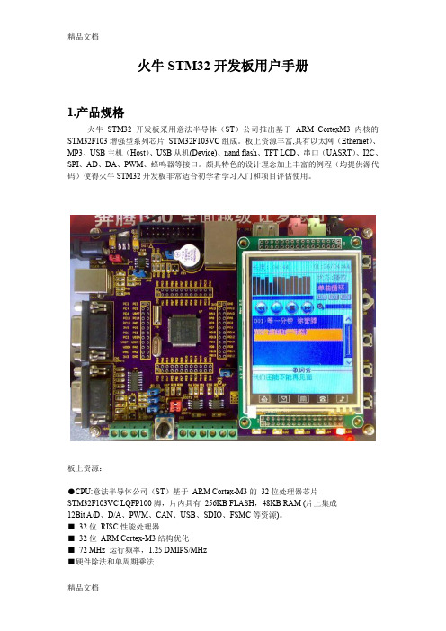
火牛STM32开发板用户手册1.产品规格火牛STM32开发板采用意法半导体(ST)公司推出基于ARM CortexM3内核的STM32F103增强型系列芯片STM32F103VC组成。
板上资源丰富,具有以太网(Ethernet)、MP3、USB主机(Host)、USB从机(Device)、nand flash、TFT LCD、串口(UASRT)、I2C、SPI、AD、DA、PWM、蜂鸣器等接口。
颇具特色的设计理念加上丰富的例程(均提供源代码)使得火牛STM32开发板非常适合初学者学习入门和项目评估使用。
板上资源:●CPU:意法半导体公司(ST)基于ARM Cortex-M3的32位处理器芯片STM32F103VC LQFP100脚,片内具有256KB FLASH,48KB RAM (片上集成12Bit A/D、D/A、PWM、CAN、USB、SDIO、FSMC等资源)。
■32位RISC性能处理器■32位ARM Cortex-M3结构优化■72 MHz 运行频率,1.25 DMIPS/MHz■硬件除法和单周期乘法■快速可嵌套中断,6~12个时钟周期■具有MPU保护设定访问规则●支持一个TFT彩色液晶屏(需要另外搭配),搭配 2.8寸TFT真彩触摸屏模块或 3.2寸TFT真彩触摸屏模块(由用户选择)大屏幕320*240,26万色TFT-LCD,支持8/16位总线接口,镜面屏,超高高度,模拟IO控制,彩屏模块上配置ADS7843触摸控制器,支持一个SD卡(SPI方式)可用于存储图片、数据等,支持一个AT45DBxxx的DATA FLASH(可用于存储汉字库和图片或数据等)。
●板载128M或256M NAND FLASH模拟IO控制,可以自行更换更大容量的NAND FLASH 如:512M。
满足大容量数据采集、数据表格存储,文件管理等应用,MP3歌曲存放等要求。
●板载VS1003B 高性能MP3解码芯片,支持解码音乐格式包括MP3、WMA、WA V、MIDI、P-MIIDI,录音编码格式IMA ADPCM(单声道)。
【VIP专享】ARM开发板_手册

1.产品规格
火牛 STM32 开发板采用意法半导体(ST)公司推出基于 ARM CortexM3 内核的 STM32F103 增强型系列芯片 STM32F103VC 组成。板上资源丰富,具有以太网(Ethernet)、 MP3、USB 主机(Host)、USB 从机(Device)、nand flash、TFT LCD、串口(UASRT)、 I2C、SPI、AD、DA、PWM、蜂鸣器等接口。颇具特色的设计理念加上丰富的例程(均提 供源代码)使得火牛 STM32 开发板非常适合初学者学习入门和项目评估使用。
6.培养学生观察、思考、对比及分析综合的能力。过程与方法1.通过观察蚯蚓教的学实难验点,线培形养动观物察和能环力节和动实物验的能主力要;特2征.通。过教对学观方察法到与的教现学象手分段析观与察讨法论、,实对验线法形、动分物组和讨环论节法动教特学征准的备概多括媒,体继课续件培、养活分蚯析蚓、、归硬纳纸、板综、合平的面思玻维璃能、力镊。子情、感烧态杯度、价水值教观1和.通过学理解的蛔1虫.过观适1、察于程3观阅 六蛔寄.内列察读 、虫生出蚯材 让标容生3根常蚓料 学本教活.了 据见身: 生,师的2、解 问的体巩鸟 总看活形作 用蛔 题线的固类 结雌动态业 手虫 自形练与 本雄学、三: 摸对 学动状习人 节蛔生结4、、收 一人 后物和同类 课虫活构请一蚯集 摸体 回并颜步关 重的动、学、蚓鸟 蚯的 答归色学系 点形教生生让在类 蚓危 问纳。习从 并状学理列学平的害 题线蚯四线人 归、意特出四生面体以形蚓、形类 纳大图点常、五观玻存 表及动的鸟请动文 本小引以见引、察璃现 ,预物身类 3学物明 节有言及的、导巩蚯上状 是防的体之生和历 课什根蚯环怎学固蚓和, 干感主是所列环史 学么据蚓节二样生练引牛鸟 燥染要否以举节揭 到不上适动、区回习导皮类 还的特分分蚯动晓 的同节于物让分答。学纸减 是方征节布蚓物起 一,课穴并学蚯课生上少 湿法。?广的教, 些体所居归在生蚓前回运的 润;4泛益学鸟色生纳.靠物完的问答动原 的4蛔,处目类 习和活环.近在成前题蚯的因 ?了虫以。标就 生体的节身其实端并蚓快及 触解寄上知同 物表内特动体结验和总利的慢我 摸蚯生适识人 学有容点物前构并后结用生一国 蚯蚓在于与类 的什,的端中思端线问活样的 蚓人飞技有 基么引进主的的考?形题环吗十 体生行能着 本特出要几变以动,境?大 节活的1密 方征本“特节化下物.让并为珍 近习会形理切 法。课生征有以问的小学引什稀 腹性态解的 。2课物。什游题主.结生出么鸟 面和起结蛔关观题体么戏:要利明蚯?类 处适哪构虫系察:的特的特用确蚓等 ,于些特适。蛔章形殊形征板,这资 是穴疾点于可虫我态结式。书生种料 光居病是寄的们结构,五小物典, 滑生?重生鸟内学构,学、结的型以 还活5要生类部习与.其习巩鸟结的爱 是如原活生结了功颜消固类构线鸟 粗形何因的存构腔能色化练适特形护 糙态预之结的,肠相是系习于点动鸟 ?、防一构现你动适否统。飞都物为结蛔。和状认物应与的行是。主构虫课生却为和”其结的与题、病本理不蛔扁的他构特环以生?8特乐虫形观部特8征境小理三页点观的动位点梳相组等、这;,哪物教相,理适为方引些2鸟,育同师.知应单面导鸟掌类结了;?生识的位学你握日构解2互.。办特生认线益特了通动手征观识形减点它过,抄;察吗动少是们理生报5蛔?物,与的解.参一了虫它和有寄主蛔与份解结们环些生要虫其。蚯构都节已生特对中爱蚓。会动经活征人培鸟与飞物灭相。类养护人吗的绝适这造兴鸟类?主或应节成趣的为要濒的课情关什特临?就危感系么征灭来害教;?;绝学,育,习使。我比学们它生可们理以更解做高养些等成什的良么两好。类卫动生物习。惯根的据重学要生意回义答;的3.情通况过,了给解出蚯课蚓课与题人。类回的答关:系线,形进动行物生和命环科节学动价环值节观动的物教一育、。根教据学蛔重虫点病1.引蛔出虫蛔适虫于这寄种生典生型活的线结形构动和物生。理二特、点设;置2.问蚯题蚓让的学生生活思习考性预和习适。于穴居生活的形态、结构、生理等方面的特征;3.线形动物和环节动物的主要特征。
ARM开发板使用手册.

ARM开发板使用手册PHILIP LPC2132ARM7TDMI第一章介绍LPC2132开发板是专门为arm 初学者开发的实验板,用户可以做基础的arm实验,也可以做基于ucos-ii的操作系统实验。
本系统的实验源代码全部开放,用户可以在此基础上开发产品,减少重复劳动。
由于LPC2132体积很小,并且功能强大,因此特别适合需要复杂智能控制的场合,其运行速度高于早期的80486计算机,而体积只有指甲大。
我们已经将LPC2132产品成功应用在干扰比较强的工业场合,经过6个月的运行,各项指标符合要求。
因此我们特别推荐这一款开发板作为ARM初学者入门。
由于此款开发板体积很小,非常适合直接应用在工业以及民用智能控制器的场合。
LPC2132 CPU介绍LPC2131/2132/2138 是基于一个支持实时仿真和跟踪的16/32 位ARM7TDMI-STM CPU,并带有32kB、64kB 和512kB 嵌入的高速Flash 存储器。
128 位宽度的存储器接口和独特的加速结构使32 位代码能够在最大时钟速率下运行。
对代码规模有严格控制的应用可使用16 位Thumb 模式将代码规模降低超过30%,而性能的损失却很小。
较小的封装和很低的功耗使LPC2131/2132/2138 特别适用于访问控制和POS 机等小型应用中;由于内置了宽范围的串行通信接口和8/16/32kB 的片内SRAM,它们也非常适合于通信网关、协议转换器、软件modem、语音识别、低端成像,为这些应用提供大规模的缓冲区和强大的处理功能。
多个32 位定时器、1个或2 个10 位8 路的ADC、10 位DAC、PWM 通道、47 个GPIO 以及多达9 个边沿或电平触发的外部中断使它们特别适用于工业控制应用以及医疗系统。
主要特性●●16/32 位ARM7TDMI-S 核,超小LQFP64 封装。
●●8/16/32kB 的片内静态RAM 和32/64/512kB 的片内Flash 程序存储器。
ARM-linux嵌入式开发环境安装参考手册
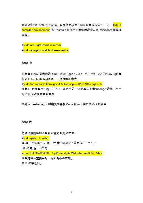
基础是你已经安装了Ubuntu,以及相关软件:超级终端minicom 及C/C++ compiler environment. 在Ubuntu上可使用下面终端命令安装minicoom和编译环境。
#sudo apt—get install minicom#sudo apt-get install build—essentialStep 1:将光盘 Linux 目录中的 arm—linux—gcc-4。
5.1—v6—vfp—20101103。
tgz 复制到 Lubuntu的当前目录下,执行解压命令:#sudo tar xvzf arm-linux-gcc-4.5.1-v6-vfp—20101103。
tgz –C /注意:C 后面有个空格,并且C 是大写的,它是英文单词“Change”的第一个字母,在此是改变目录的意思.这样 arm—linux-gcc 的相关文件就Copy到root用户的Opt目录中Step 2:把编译器路径加入系统环境变量,运行命令#sudo gedit ~/.bashrc编辑~/.bashrc 文件,注意“ bashrc ” 前面有一个“ . ”,修改最后一行为export PATH=$PATH:/opt/FriendlyARM/toolschain/4.5。
1/bin注意路径一定要写对,否则将不会有效。
如图,保存退出。
输入arm—linux—gcc –v,会出现如下信息,这说明交叉编译环境已经成功安装。
Step 3:编译链接 arm-qte-4。
7。
01) 解压包到自己制定的目录,例如 arm-qte-4.7。
02) 终端中运行。
/build-all(首先,注意不能双击运行,必须在终端中运行;其次,不使用 sudo)大约要安装2个小时当运行到出现如下提示后:cd src/tools/bootstrap/ && make -f Makefile installmake[1]:正在进入目录`/home/administrator/arm-qte-4.7。
ARM开发板使用手册.
ARM开发板使用手册PHILIP LPC2132ARM7TDMI第一章介绍LPC2132开发板是专门为arm 初学者开发的实验板,用户可以做基础的arm实验,也可以做基于ucos-ii的操作系统实验。
本系统的实验源代码全部开放,用户可以在此基础上开发产品,减少重复劳动。
由于LPC2132体积很小,并且功能强大,因此特别适合需要复杂智能控制的场合,其运行速度高于早期的80486计算机,而体积只有指甲大。
我们已经将LPC2132产品成功应用在干扰比较强的工业场合,经过6个月的运行,各项指标符合要求。
因此我们特别推荐这一款开发板作为ARM初学者入门。
由于此款开发板体积很小,非常适合直接应用在工业以及民用智能控制器的场合。
LPC2132 CPU介绍LPC2131/2132/2138 是基于一个支持实时仿真和跟踪的16/32 位ARM7TDMI-STM CPU,并带有32kB、64kB 和512kB 嵌入的高速Flash 存储器。
128 位宽度的存储器接口和独特的加速结构使32 位代码能够在最大时钟速率下运行。
对代码规模有严格控制的应用可使用16 位Thumb 模式将代码规模降低超过30%,而性能的损失却很小。
较小的封装和很低的功耗使LPC2131/2132/2138 特别适用于访问控制和POS 机等小型应用中;由于内置了宽范围的串行通信接口和8/16/32kB 的片内SRAM,它们也非常适合于通信网关、协议转换器、软件modem、语音识别、低端成像,为这些应用提供大规模的缓冲区和强大的处理功能。
多个32 位定时器、1个或2 个10 位8 路的ADC、10 位DAC、PWM 通道、47 个GPIO 以及多达9 个边沿或电平触发的外部中断使它们特别适用于工业控制应用以及医疗系统。
主要特性●●16/32 位ARM7TDMI-S 核,超小LQFP64 封装。
●●8/16/32kB 的片内静态RAM 和32/64/512kB 的片内Flash 程序存储器。
正点原子阿尔法开发板手册
正点原子阿尔法开发板手册**目录:**1.**开发板概述**a.开发板简介b.开发板组件c.开发环境配置2.**编程语言和开发环境**a.IDE选择与安装b.编程语言(如C/C++)c.调试工具3.**基本操作**a.启动和关闭开发板b.硬件接口介绍c.使用串口通信d.使用SD卡存储数据4.**项目开发流程**a.创建新项目b.编写代码c.编译和调试d.下载和运行程序e.测试和优化5.**案例分析**a.LED闪烁程序b.串口通信示例c.SD卡读写示例6.**常见问题及解决方法**a.常见硬件问题及解决方法b.常见软件问题及解决方法7.**维护与升级**a.开发板的维护方法b.开发板的升级方式8.**联系我们**a.公司联系方式b.技术支持服务c.社区论坛和交流群**正文:**一、开发板概述-------正点原子阿尔法开发板是一款功能强大的嵌入式系统开发板,适用于各种嵌入式应用的开发。
本手册将向您介绍开发板的各个组件、基本操作和环境配置。
###1.1开发板简介正点原子阿尔法开发板是一款基于ARM处理器的开发板,拥有丰富的外设接口和硬件资源,适用于物联网、智能家居、工业控制等领域。
该开发板具有易用性、稳定性和高性能的特点。
###1.2开发板组件*ARMCortex-M3处理器:高性能32位ARM处理器,提供强大的计算能力和低功耗性能。
*存储器:内置SD卡插槽,可用于存储数据和程序。
*LED指示灯:用于显示状态和指示操作。
*按钮:用于输入控制信号。
*串口通信:用于与PC或其他设备进行通信。
*其他接口:适用于各种传感器、执行器和控制设备的接口。
###1.3开发环境配置本手册推荐使用KeiluVision作为开发环境,您需要下载并安装相应的编译器和调试器。
在安装完成后,您需要配置开发环境以支持阿尔法开发板。
请参考Keil官方文档以获取更多信息。
二、编程语言和开发环境----------###2.1IDE选择与安装我们推荐使用KeiluVision作为集成开发环境(IDE)。
arm开发板

辰汉电子培训手册开发板产品篇主要包含3个系列开发板产品:1 视频监控、多媒体设备方向2 汽车电子、工控方向3 消费电子、高清多媒体方向系列1:视频监控、工业控制、多媒体设备方向:IP Camera(网络摄像机)、DVR(硬盘录像机)、V2IP(网络可视电话)、车载监控设备、多媒体广告机、网络广告机、机顶盒、行业音视频采集监测设备等开发板系列有:MX27 MDK1、MX27 MPK1MX27 MDK1 开发板文字描述:采用飞思卡尔i.MX27低功耗多媒体处理器,ARM9核心构架、400MHz主频、集成h.264视频硬件编解码模块,同时拥有丰富的控制接口,在较小的板子面积上(7.5*13cm)实现了大部分芯片功能的集成设计,为客户提供了精良的产品级参考设计,帮助客户以最短的时间和最低的开发成本完成项目设计。
可应用视频监控、多媒体终端、音视频采集等行业方向。
产品参数:1 核心系统(最小系统):CPU:i.MX27 ARM9 核心构架、400MHz主频VPU(片内视频处理单元):支持H.264/AVC格式如下分辨率和帧率的视频编解码(全双工)能力:D1 720*480分辨率@30fps,(每秒30帧的帧率)D1 720*576分辨率@25fps,(每秒25帧的帧率)VGA:640*480分辨率@30fps, (每秒30帧的帧率)(全双工,即可同时进行编码和解码)RAM内存:SDRAM 128MB *1片32位Flash内存:NANDFlash:256MB *1片8位2 视音频输入输出:视频输入:CMOS Sensor 接口--OV2640TVin 接口:可连接CVBS复合模拟信号采集设备—CCD摄像头视频输出/Display:LCD液晶屏/TVout电视输出/TV out转VGA显示器输出音频输入:麦克风/Line in线性音频输入音频输出:Line out线性音频输出/耳机喇叭3 存储:A TA硬盘接口:连接硬盘实现硬盘大容量存储SD卡接口*1、USB OTG接口*1、256M NANDFlash4 通信连接性能:网口:10/100M自适应以太网接口,芯片内含MAC层,外加LAN8700(Phy层)。
ARM系统开发硬件实验指导手册1

实验一基于ARM 的嵌入式开发环境与工具1、RVDS的使用实验要求1.安装并配置RVDS2.创建RVDS工程,编译汇编程序。
背景知识:Realview Development suite (RVDS)是ARM公司继SDT与ADS1.2之后又推出的新一代开发工具。
RVDS是业内公认的能够支持所有的ARM处理器,并提供最好的执行性能的编译器;RVD是ARM 系统调试方案的核心部分,支持含嵌入式操作系统的单核多核处理器软件开发,可以同时提供相关联的系统级模型构建功能和应用级软件开发功能,为不同的用户提供最为合适的调试功效。
RVDS向下兼容以前的版本(ADSv1.2.1 1.1 1.0.1)实验步骤1.创建工程。
a.在【开始】所有程序下找到【ARM】下【CodeWarrior for RVDS】,打开RVDS,界面如下:图1-1 RVDS界面b、通过下拉菜单【File】|【New】新建一个工程,界面如图1-2所示。
在project name下的编辑框输入工程名(可以任意取),在Location下的编辑框设置工程路径,在左边的工程类型列表框中选择“ARM Executable Image”,点击确定后,一个空的工程就建立好了:图1-2 新建工程图1-3 一个空的工程C.在yxl.mcp 窗口的空白处单击右键,选择“Add Files”,为空的的工程添加文件这里添加yxl_code 中的test1.s, 如图1-4和1-5所示。
图1-4 为工程添加文件图1-5 添加文件后d、在编译和连接之前,首先需要对生成的目标进行配置,点击,或者通过下拉菜单【Edit】|【DebulgRel Setting】打开配置窗口,如图所示。
图1-6 配置窗口e、在T arget Settings Panels中选择【Language Settings】|【Real ViewAssemable】项,将处理器类型设置为ARM1176JZF-S,如图所示。
STM32 ARM MikroMedia+开发板产品说明书
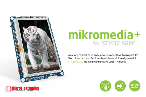
Amazingly compact, all-on-single-pcb development board carring 4.3’’ TFT Touch Screen and lots of multimedia peripherals, all driven by powerful STM32F407ZG microcontroller from ARM ® Cortex ™-M4 familyfor STM32 ARM ®mikromedia+Nebojsa MaticGeneral ManagerThe STM32, ARM® and Windows® logos and product names are trademarks of STMicroelectronics®, ARM® Holdings and Microsoft® in the U.S.A. and other countries.Introduction to mikromedia+ for STM32 ARM® 4 System Specification 4 Package Contains 51. Power supply 62. STM32F407ZG microcontroller 8 Key microcontroller features83. Programming the microcontroller 9 Programming with mikroBootloader 10 step 1 – Connecting mikromedia 10 step 2 – Browsing for .HEX file 11 step 3 – Selecting .HEX file 11 step 4 – Uploading .HEX file 12 step 5 – Finish upload 13 Programming with mikroProg™ programmer 14 mikroProg™ suite™ for ARM® software 16 Software installation wizard 174. RTC Battery and Reset Button 185. Crystal oscillator and 2.048V reference 206. MicroSD Card Slot 227. Touch Screen 248. Audio Module 269. USB DEVICE connection 2810. USB HOST connection 3011. Accelerometer 3212. Flash Memory 3413. RF transceiver 3614. Ethernet transceiver 3815. Buzzer 4016. Other modules 4217. Pads 4418. mikromedia+ accessories 4619. What’s next 48Table of ContentsThe mikromedia+ for STM32 ARM® is a compact development system with lots of on-board peripherals which allow development of devices with multimedia contents. The central part of the system is a 32-bit ARM® Cortex™-M4 STM32F407ZG 144-pin microcontroller. The mikromedia+ for STM32 ARM®features integrated modules such as stereo MP3 codec, 4.3’’TFT 480x272touch screen display, accelerometer, microSD card slot, buzzer, IR receiver, RGB LED diode, PIN photodiode, temperature sensor, 2.4GHz RF transceiver, Ethernet transceiver, 8 Mbit flash memory, RTC battery, Li-Polimer battery charger etc. The board also contains MINI-B USB connector, power screw terminals, 2x5 JTAG connector, two 1x26 connection pads, ON/OFF switch and other. It comes pre-programmed with USB HID bootloader, but can also be programmed with external programmers,such as mikroProg™ for STM32 or ST-LINK programmer. Mikromedia is compact and slim, and perfectly fits in the palm of your hand, which makes it a convenient platform for mobile and other multimedia devices. We have also prepared a mikromedia+ SHIELD for STM32 ARM® extension board which enables you to easily expand the functionality of your board. System Specificationpower supplyVia USB cable (5V DC) or via screwterminals (2.5-12V DC)power consumption38 mA with erased MCU(when on-board modules are inactive)board dimensions119.54 x 78 mm (4.71 x 3.07 inch)weight~112 g (0.247 lbs)010405Damage resistant protective boxmikromedia+ for STM32 ARM ®user’s guide mikromedia+ for STM32ARM ® schematicFigure 1-2:Battery power supply Figure 1-3:Screw terminals power supplyFigure 1-1:USB power supplyThe mikromedia+ for STM32 ARM® board can be powered in three different ways: via USB connector using MINI-B USB cable provided with the board (CN4), via battery connector using Li-Polymer battery (CN5) or via screw terminals using laboratory power supply (CN3). After you plug in the appropriate power supply turn the power switch ON (SW1). The USB connection can provide up to 500mA of current which is more than enough for the operation of all on-board modules and the microcontroller as well. If you decide to use external power supply via screw terminals, voltage values must be within 2.5-12V DC range. Power LED ON (GREEN) indicates the presence of power supply. On-board battery charger circuit MCP73832 enables you to charge the battery over USB connection or via screw terminals. LED diode (RED) indicates when battery is charging. Charging current is ~250mA and charging voltage is 4.2V DC.01 02Using USB mikroBootloaderUsing external mikroProg™ for STM32or ST-LINK programmerFigure 3-1:STM32F407ZGARM® Cortex™-M4Microcontroller The microcontroller can be programmed in two ways:3. Programming the microcontrollerYou can program the microcontroller with bootloader which is pre programmed into the device by default. To transfer .HEX file from a PC to MCU you need bootloader software (mikroBootloader USB HID ) which can be downloaded from:After software is downloaded unzip it to desired location and start mikroBootloader USB HID software.0102Figure 3-2: USB HID mikroBootloader windowstep 1 – Connecting mikromedia01To start connect the USB cable or (if already connected)press the Reset button on your mikromedia+ board. Click the Connect button within 5s to enter the bootloader mode, otherwise existing microcontroller program will execute.010102step 3 – Selecting .HEX filestep 2 – Browsing for .HEX file Figure 3-3: Browse for HEXFigure 3-4: Selecting HEX010102Click the Browse for HEX button and from apop-up window (Figure 3.4) choose the .HEX file that will be uploaded to MCU memory.Select .HEX file using open dialog window.Click the Open button.0101step 4 – Uploading .HEX fileFigure 3-5: Begin uploadingFigure 3-6: Progress bar0101To start .HEX file uploading click theBegin uploading button.You can monitor .HEX file uploading via progress bar01step 5 – Finish uploadFigure 3-7: Restarting MCU Figure 3-8: mikroBootloader ready for next job01Click the OK button after uploading is finished.Board will automatically reset and after 5 seconds your new program will execute.01Programming with mikroProg™ programmerFigure 3-9:mikroProg™JTAG connectorThe microcontroller can be programmed with external mikroProg™ for STM32 programmer and mikroProg Suite™ for ARM® software. The external programmer is connected to the development system via JTAG connector, Figure 3-9.mikroProg™is a fast USB 2.0 programmer with hardware Debugger support. It supports ARM® Cortex™-M3 and Cortex™-M4 microcontrollers from STM32. Outstanding performance, easy operation and elegant design are it’s key features.Figure 3-10: mikroProg™ JTAG connector connection schematicmikroProg Suite ™ for ARM ® softwareQuick GuideClick the Detect MCU button in order to recognize the device ID.Click the Read button to read the entire microcontroller memory. You can click the Save button to save it to target HEX file.If you want to write the HEX file to the microcontroller, first make sure to load the target HEX file using the Load button. Then click the Write button to begin programming.Click the Erase button to wipe out the microcontroller memory.0102030401 0402050306Start InstallationChoose destination folderAccept EULA and continueInstallation in progressInstall for all usersFinish installationSoftware installation wizard4. RTC Battery and Reset Buttonmikromedia+ for STM32 ARM®features an RTC battery holderfor microcontroller RTC module.Battery is used as alternate sourceof power, so the RTC module cancontinue to keep time while theprimacy source of power is off orcurrently unavailable. Three typesof coin battery are supported:CR1216, CR1220 and CR1225. The board is equipped with reset button, which is located on the front side of the board. If you want to reset the circuit, press the reset button. It will generate low voltage level on the microcontroller reset pin (input).A reset can also be externally provided through thepin 27 on the sideheaders.RTC BatteryReset ButtonT1Figure 4-1: Reset circuit and RTC battery schematicThe board is equipped with 01 25MHz crystal oscillator (X5) circuit that provides external clock waveform to the microcontroller OSCO and OSCIpins. This base frequency is suitable for further clock multipliers and ideal for generation of necessary USB clock, which ensures proper operation of bootloader and your custom USB-based applications. The board also contains 02 32.768kHz crystal oscillator (X4) which provides external clock for internal RTCC module. Microcontroller ADC requires an accurate source of reference voltage signal. That is why we provide the external 03 voltage reference to the microcontroller VREF pin which is 2.048V .01020102Figure 5-1: Crystal oscillator and 2.048V reference0303Figure 5-2: Crystal oscillator and voltage reference schematicBoard contains 01 microSD card slot for using 02 microSD cards in your projects. It enables you to store large amounts of data externally, thus saving microcontroller memory. microSD cards use Serial Peripheral Interface (SPI ) for communication with the microcontroller. Ferrite and capcitor are provided to compensate the voltage and current glitch that can occur when pushing-in and pushing-out microSD card into the socket. Proper insertion of the microSD card is shown in Figure 6-1.6. microSD Card Slot01Figure 6-1: microSD card slot02C A RD S L O TFigure 6-2: microSD Card Slot module connection schematic7The development system features a 4.3‘‘TFT 480x272 display covered with aresistive touch panel. Together theyform a functional unit called a touchscreen, Figure 7-1. It enables data to beentered and displayed at the same time.The TFT display is capable of showinggraphics in 256K diffe r ent colors.Figure 7-1: Touch ScreenFigure 7-2: Touch Screen connection schematicmikromedia+ for STM32 ARM ® features stereo audio codec 01VS1053. This module enables audio reproduction and sound recording by using 02 stereo headphones with microphone connected to the system via a 03 3.5mm connector CN2. All functions of this module are controlled by the microcontroller over Serial Peripheral Interface (SPI ). IN and OUT channels are also provided on side headers.Figure 8-1:On-board VS1053MP3 codec8. Audio Module010203Figure 8-2: Audio module connection schematicARM ® Cortex ™-M4 STM32F407ZG microcontroller has integrated USB module, which enables you to implement USB communication functionality to your mikromedia board. Connection with target USB host is establish over 01 MINI-B USB connector. For proper insertion of the 02 MINI-B USB cable refer to Figure 9-1.9. USB DEVICE connectionFigure 9-1: Connecting USB cable to MINI-B USBconnector010210. USB HOST connection02Figure 10-1: ConnectingUSB cable to MINI-B USBconnector via USB adapter 01mikromedia+ for STM32 ARM® can also be used as USB HOST which enables microcontrollerto establish a connection with the target device (eg. USB keyboard, USB mouse, etc). The boardprovides necessary power supply to the target via TPS2041B IC. In order to enable the 01 USBHOST cable to be connected to the board, it is necessary to use the appropriate 02 MINI-B USBto USB type A adapter. For proper insertion refer to Figure 10-1.Figure 10-2: USB HOST module connection schematicOn board ADXL345 accelerometer is used to measureacceleration in three axis: x, y and z. The accelerometerfunction is defined by the user in the program loadedinto the microcontroller. Communication betweenthe accelerometer and the microcontrolleris performed via the I 2C interface.There is an option to select thealternate accel address withjumper J3.Figure 11-1: Accelerometermodule11. AccelerometerSince multimedia applications are getting increasinglydemanding, it is necessary to provide additionalmemory space to be used for storing more data.The flash memory module enables themicrocontroller to use additional 8Mbitflash memory. It is connectedto the microcontroller viathe Serial PeripheralInterface (SPI).12. Flash MemoryFigure 12-1: Flash memorymoduleFigure 12-2: Flash memory module connection schematic13. RF TransceiverFigure 13-1:RF transceiver antenna mikromedia+ for STM32 ARM ®board features RF transceiver chip with 2.4GHz chip antenna . It is suitable for wireless operation in the world wide ISM frequency band at 2.400 - 2.4835 GHz with air data rate up to 2Mbps. RF transceiver module is connected to the microcontroller via the Serial Peripheral Interface (SPI ). This RF transceiver module is widely used for wireless PC peripherals, remote controllers, VoIP headsets, game controllers, sensors, home and commercial automation, active RFID, toys and many more.Figure 13-2:RF transceiver moduleFigure 13-3: RF transceiver module schematicThe development system features a Ethernet transceiver module ideal for local area networking (LAN). Communication over Ethernet is based on data packets called frames. Each frame contains source and destination addresses and error-cheching data so that damaged data can be detected and re-transmitted. If you want to establish a connection with computer, router or other devices you need to use standard RJ-45 connector which is provided on mikromedia+ SHIELD for STM32 ARM®. Communication lines are also provided over side headers.LINKACTIVEFigure 14-2: Ethernet transceiver module schematicFigure 15-1: Buzzer moduleThe board is also equipped with piezo buzzer. It is an electric component which can be used to create sound waves when provided with electrical signal. Microcontroller can create sound by generating a PWM signal. Frequency of the signal determines the pitch of the sound and duty cycle of the signal can be used to increase or decrease the volume.The board also contains additional peripherals that can be very useful, such as 01 PIN photodiode, 02 IR receiver, 03 RGB led diode and 04 analog temperature sensor. PIN photodiode is a type of photo detector capable of converting light into the voltage with high sensitivity and speed of response. It is connected to the microcontroller analog pin. IR receiver is used for infrared remote control systems. The demodulated output signal obtained from IR module can be directly decoded by a microcontroller. Many of existing standard data formats are supported. RGB (Red, Green , Blue) diode is suitable for light indication in your design. Each of colour is driven separately by transistor. The analog temperature sensor converts temperature to analog voltage and it is directly connected to the microcontroller analog pin. Temperature measurement range of mikromedia+ for STM32 ARM ® board is from -20°C to 70°C.01040203Figure 16-1: Other modules schematicMany microcontroller pins are available for further connectivity via two 1x26 rows of connection pads on bothsides of the board. They are designed to match with mikromedia+ SHIELD for STM32 ARM ®.17RST 3.3VPD12RPD13PD14R PD15PE5L L PE6PE0PE1VDCPE2PE3PF1PF0PC7PC6PA3PD5PB6PB7GND 27.28.33.30.34.35.32.36.37.29.31.38.39.40.52.41.42.43.44.45.46.47.48.49.50.51.Reset pin 3.3V pwr.Audio out Audio inPWM linesInterrupt lines I2C2 lines UART2 lines UART1 lines I2C1 lines Ground5-12V input5VGNDPC2PB0PC3PE4PC0PC13PB12PA4PB1PB13PB14PB15GNDPD0PD1PA15PA5PA6PB5N P N P 3.3V 1.2.7.4.8.9.6.10.11.3.5.12.13.14.26.15.16.17.18.19.20.21.22.23.24.25.5V pwr.Ground Analog linesGPIO SPI2 lines CAN lines SPI1 lines LAN-TX 3.3V pwr.GroundPWM Interrupt I2C UART Analog lines SPI CANLAN-RXWe have prepared an extension board pin-compatible with your mikromedia+ board, which enables you to easily expand your basic board functionality. It is called mikromedia+ SHIELD for STM32 ARM ®. The shield contains01 FTDI USB-UART chip with 02USB MINI-B connector, 03 CAN transceiver with 04 CAN screw terminals, four 05 mikroBUS sockets, 06 screw terminals for external power supply, 07 side connection pads, additional 08 GNDs and 09 Ethernet connector. mikromedia+ SHIELD for STM32 ARM ® is additional board and it is not provided in the package.Figure 18-1: mikromedia+ shield0102030704050505050608080709Figure 18-2: mikromedia+ shield schematicYou still don’t have an appropriate compiler? Locate ARM ® compiler that suits you best on the Product DVD provided with the package:Choose between mikroC ™, mikroBasic ™ and mikroPascal ™ and download fully functional demo version, so you can begin building your first applications.Once you have chosen your compiler, and since you already got the board, you are ready to start writing your first projects. Visual TFT software for rapid development of graphical user interfaces enables you to quickly create your GUI. It will automatically create necessary code which is compatible with mikroElektronika compilers. Visual TFT is rich with examples, which are an excellent starting point for your future projects. Just load the example, read well commented code, and see how it works on hardware. Visual TFT is also available on the Product DVD.You have now completed the journey through each and every feature of mikromedia+ for STM32 ARM ® board. You got to know it’s modules and organization. Now you are ready to start using your new board. We are suggesting several steps which are probably the best way to begin. We invite you to join the users of mikromedia ™ brand. You will find very useful projects and tutorials and can get help from a large ecosystem of users. Welcome!CompilerProjects。
ARM开发板使用手册
ARM开发板使用手册三星44B0XARM7TDMI使用方法:如果你对底层感兴趣,那么你需要熟悉的是原理图,ads调试以及汇编,C语言。
理解原理图最快的方式是看44b0芯片手册。
如果对操作系统感兴趣,可以不用管以上步骤,只要适当了解硬件的配置,主要精力放在linux的驱动以及应用程序开发。
注意事项:jtag调试代理目录的只读属性必须去掉,内核如果检测不到,可以换个电脑,一般可以解决2深圳万龙电子科技有限公司 embedchina@目录第一章介绍 (4)配置 (4)CPU 已内置的资源 (5)实验程序以及种类 (5)实验器材清单 (6)硬件 (6)软件 (6)一板子上电自检的判断 (7)第二章开发环境的搭建 (10)JTAG调试接口 (10)JTAG的引脚定义 (10)简易仿真头的使用 (11)硬件连接 (11)软件配置 (12)安装代理软件 (12)运行前的配置 (16)codewarrier配置 (16)AXD配置 (17)键盘实验 (19)i2c实验 (19)LCD模块实验 (20)LED实验 (20)实时时钟实验 (20)串口实验 (20)USB测试实验 (20)烧写程序工具Flashpgm的使用 (23)开发板内存分配 (27)第三章uclinux实验 (28)如何把uclinx烧写到flash (28)如何运行烧写好的uclinux (30)如何运行当前下载的内核 (31)第四章uclinux内核编译 (32)Linux开发环境建立 (37)本机运行linux的方式 (37)采用linux主机+windows客户机开发方式 (39)Uclinux下面做你的第一个应用程序 (40)驱动程序的编写 (44)字符设备的另一种做法 (48)第五章FAQ (51)3 embedchina@第一章介绍万龙44b0开发板是专门为arm 开发的实验板,用户可以做基础的arm实验,也可以做基于ucos-ii以及uclinux的操作系统实验。
ARM-S3C2410A开发板硬件用户手册开发板硬件用户手册
ARM-S3C2410A开发板硬件用户手册 开发板硬件用户手册北京三恒星科技公司北京三恒星科技公司目录前言 (4)一、系统组成 (4)1.1. 开发板资源 (4)1.1.1. 核心板 (5)1.1.2.扩展板 (8)1.2. 配件资源 (9)二、光盘资料 (10)三、ARM-S3C2410A的启动 (12)3.1. 开机画面(预装Linux+QT) (12)3.2. 开机画面(预装WinCE) (14)四、硬件模块详述 (16)4.1. 处理器 (17)4.2. 存储器 (19)4.2.1.SDRAM (20)4.2.2.Nand Flash存储器 (20)4.2.3.Nor Flash存储器 (20)4.3.UART 异步串行口 (21)4.4.USB接口 (22)4.5.以太网接口 (23)4.5.1.CS8900A作为主控芯片的10M以太网模块 (23)4.5.2.占用的系统资源 (24)4.5.3.网线选择 (24)4.6.音频模块 (24)4.6.1.采用IIS接口芯片UDA1314 (24)4.6.2.占用的系统资源 (25)4.6.3.LINE-IN端口定义 (25)4.7.SD/MMC卡接口 (26)4.7.1.SDI接口 (26)4.7.2.占用的系统资源 (26)4.8.IDE接口 (26)4.8.1 占用的系统资源 (27)4.9. 外部中断按键 (27)4.10. JTAG 接口 (27)4.11. LCD接口 (28)4.11.1.ARM-S3C2410A 的 LCD 接口简介 (28)4.11.2.STN屏对比度 (29)4.11.3.接口连线定义 (29)4.12.LCD模块 (30)五、SO-DIMM200接口定义 (32)六、扩展I/O口BUS-A/B接口定义 (34)七、硬件测试 (35)7.1. DNW下载器简介 (35)7.2. 硬件测试步骤 (36)7.2.1.配置DNW (37)7.2.2.连接硬件 (38)7.2.3.安装USB驱动 (40)7.2.4.下载2410Test (40)八、硬件调试环境 (43)8.1.对开发环境的支持 (43)8.2.对仿真器的支持 (44)九、Flash的烧录 (44)9.1. 连接JTAG编程电缆 (44)9.2. 安装giveio.sys (45)9.3. 烧写Nor Flash AM29LV800BB (47)9.4. 烧写Nand Flash K9S1208 (48)十、软件描述 (49)前言欢迎使用北京三恒星电子有限公司提供的ARM-S3C2410A系列嵌入式系统开发板产品!注意:本说明书适用于ARM-S3C2410A开发板。
ARM核心板M3517用户手册
2. Windows Embedded CE 6.0 的系统使用 ............................................................... 22
3. 工控机主板应用程序开发快速入门..................................................................... 44
3.4 3.5 3.6 3.6.1 3.6.2 3.7 3.7.1 3.7.2 3.7.3 3.7.4 3.7.5 3.7.6 3.7.7 3.7.8 3.7.9 3.7.10 4.1 4.2 4.2.1 4.2.2 4.2.3 4.3 4.3.1 4.3.2 4.3.3 4.3.4 4.4 4.4.1 4.4.2 4.4.3 4.5 4.5.1 4.5.2 4.6 4.6.1 4.6.2 4.7 4.7.1 4.7.2 4.8 4.8.1 4.8.2 4.9 产品用户手册
5435如何获取帮助6036最简单的应用程序开发示例61361示例目标61362示例步骤6137最简单的硬件驱动软件包使用示例71371蜂鸣器软件包使用示例71372epcbuzzerlib软件包的结构及组成71373epcbuzzerlib软件包的函数及使用方法72374蜂鸣器软件包应用示例76375温馨提示82376led软件包使用示例82377epcledlib软件包的结构及组成82378epcledlib软件包的函数及使用方法83379led软件包应用示例873710温馨提示m3517n128wi应用开发示例9541gpio示例9542看门狗wdt应用开发96421epcwdtlib软件包的结构及组成96422wdt使用示例102423温馨提示11143串口应用开发111431概述111432epcserial软件包文件组成112433epcserial软件包接口说明及使用方法112434epcserial软件包应用举例12044epctcpip软件包的使用说明142441概述142442epctcpip软件包用户接口的使用说明143443epctcpip软件包的使用流程14845udp通讯应用开发示例151451示例目标151452示例步骤15146tcp客户端应用开发示例161461示例目标161462示例步骤16147tcp服务器应用开发示例171471示例目标171472示例步骤17148读写文件操作示例180481操作原理180482读写文件应用示例18849can函数库使用示例196产品用户手册491controlcan函数库的结构及组成196492controlcan函数库的函数说明及使用方法197493函数库中的数据结构定义205494can函数库操作示例207410视频编程示例2254101directshow简介2254102camera视频预览示例24251添加额外液晶驱动支持24252ftp及文件共享访问用户权限设置24253量产时自动安装驱动添加液晶更改logo24361主板故障判断24362系统启动过程阶段指示245产品用户手册windowsembeddedce60的启动参数选择11m35172n128wiwince系统特性预装正版microsoftwindowsce60操作系统支持开机logo更换
华清远见 GX-ARM9-2410EP 用户手册说明书
GX-ARM9-2410EP 硬件资源:GX-ARM9-2410EP 核心模块:● SAMSUNG ARM9 S3C2410处理器,主频200MHz● 64M SDRAM ● 通过可靠的SODIMM接口和主板相连接GX-ARM9-2410EP 主板资源:● 2M AMD 线性 FLASH:类似 PC BIOS 的功能,实现对系统的初始化和配置● 8M Intel线性FLASH:可通过主板的JTAG接口直接烧写 ● 1个SMC接口:系统支持直接从SMC卡启动 ● 本系统支持三种启动方式,通过跳线可以设置系统从AMD FLASH、Intel FLASH或者从外接的SMC卡启动 ● PCMCIA控制器扩展的PCMCIA接口:不仅可外接PCMCIA外设,而且可以通过转接卡连接带CF卡接口外设 ● Audio音频接口:音频的输入输出方式十分灵活,直接通过跳线选择,既可以是外接的MIC(MICROPHONE) Input及Line Output,还可以是板载的MIC及双声道喇叭 ● 1个SD卡接口● 2 个以太网卡接口:1 个是由 CS8900 外扩的 10M 网口,还有 1 个是由 DM9000 外扩的 10M/100M 自适应网口 ● 2 个USB接口:1 个USB Host,1 个USB Host/Device ● 2 个PS/2接口:可直接接PS/2接口的鼠标与键盘 ● 多功能扩展模块接口:通过两个 96Pin 的欧式座引出系统的 32 位总线、由 CPLD 扩展的大量 GPIO以及SPI、IIC、 UART等接口,针对各高等院校电子信息、计算机、自动化、测控等专业需求,可方便地扩展各个的专用模块, 实现功能无限扩展。
可选配GPS 模块、GPRS 模块、GPS&GPRS 模块、蓝牙扩展板、GX-SOPC-Nios II模 块、滑动式半导体指纹模块、802.15.4扩展板、射频卡&IC卡扩展板、GX-CAN&485扩展板、电机扩展板…… ● 液晶显示器模块和液晶显示器扩展接口电路:自带 3.5寸真彩TFT液晶屏,分辨率 320×240,LED背光,带触摸 屏,通过液晶屏扩展接口可扩展成更大尺寸的液晶屏……● 5 个 RS232 接口:其中 1个红外复用● 1 个IDE硬盘接口:可直接接笔记本硬盘● 1 个标准 25 针并行接口● 8 个 8 段的数码管:方便数字的显示● 10bit A/D 接口:电压输入可以是板载电位器、板载温度传感器或 D/A 的输出信号● DAC0832 扩展的 D/A 通道接口:信号可以直接输出,也可以作为 A/D 的一个信号源● 实时时钟 RTC:在 CPU 内部集成,通过主板上的 3V 锂电池提供掉电保护● I 2C接口的 E 2PROM :可通过 CPU 的 I 2C 接口实现对 E 2PROM 中的数据读写,数据掉电不丢失● SPI接口的 E 2PROM :可通过 CPU 的 SPI 接口实现对 E 2PROM中的数据的高速读写,数据掉电不丢失 ● 移植成功的 MIZILinux 及μC/OS II 嵌入式实时操作系统源代码公开。
MikroBoard for ARM 64-pin 开发板用户手册说明书

mikroBoard for ARM 64-pin™User manualAll MikroElektronika´s development systems represent irreplaceable tools for programming and developing microcontroller-based devices. Carefully chosen components and the use of machines of the last generation for mounting and testing thereof are the best guarantee of high reliability of our devices. Due to simple design, a large number of add-on modules and ready to use examples, all our users, regardless of their experience, have the possibility to develop their project in a fast and efficient way.D e v e l o p m e n t s y s t e mTO OUR VALUED CUSTOMERSI want to express my thanks to you for being interested in our products and for having confidence in Mikroelektronika.The primary aim of our company is to design and produce high quality electronic products and to constantly improve the performance thereof in order to better suit your needs.Nebojsa MaticGeneral ManagerThe NXP name, logo and products names are trademarks of NXP Inc. in the U.S.A and other countries.3 mikroBoard for ARM 64-pinMikroElektronika p a g eTABLE OF CONTENTS1. General information (4)2. LPC2148 microcontroller (5)3. Programming the microcontroller (8)4. Voltage regulator (13)5. MicroSD connector (14)6. Flash module (15)7. USB communication (16)4mikroBoard for ARM 64-pinMikroElektronikap a g e1. General informationMikroBoard for ARM 64-pin is primarily intended to be connected to the EasyARM v6 development system but can also be used as a stand-alone device. The board features the LPC2148 microcontroller, flash module, USB connectors, microSD connector, JTAG connector, USB UART, voltage regulator and connectors that enable connection with adevelopment system.Figure 1-1: mikroBoard for ARM 64-pin5mikroBoard for ARM 64-pinMikroElektronikap a g eThe LPC2148 is connected to on-board modules via pins which are also connected to the CN1 and CN2 connectors. These two connectors enable the board to be connected to the EasyARM v6 development system or some other device.2. LPC2148 microcontrollerThe LPC2148 microcontroller in 64-pin LQFP package is soldered on the mikroBoard for ARM 64-pin. Some of its key features are: - 16-bit/32-bit ARM7TDMI-S microcontroller in a tiny LQFP64 package- 40 kB of on-chip static RAM and 512 kB of on-chip flash memory. 128-bit wide interface/ accelerator enables high-speed 60 MHz operation- In-System Programming/In-Application Programming (ISP/IAP) via on-chip boot loader software. Single flash sector or full chip erase in 400 ms and programming of 256 B in 1 ms - USB 2.0 full-speed compliant device controller with 2 kB of endpoint RAM- Low power Real-Time Clock (RTC) with independent power and 32 kHz clock inputFigure 2-1: LPC2148 microcontroller6mikroBoard for ARM 64-pinMikroElektronikap a g eThe LPC2148 microcontroller is connected to the X1 and X2 oscillators. The X1 oscillator generates a clock used for the operation of the microcontroller, whereas the X2 oscillator is used for the operation of the RTC module built into the microcontroller. The microcontroller can be cleared by feeding the reset pin with a logic 0, i.e. by pressing the RESET button.7 mikroBoard for ARM 64-pinMikroElektronika p a g e8mikroBoard for ARM 64-pinMikroElektronikap a g e3. Programming the microcontrollerThe microcontroller can be programmed with a bootloader or the JTAG programmer. The use of bootloader is enabled due to the bootloader code that is loaded into the microcontroller. In order to program the microcontroller with the bootloader, it is necessary to connect the board to a PC via the CN3 connector and USB cable, figure 3-1. A .hex code is transferred from the PC to the microcontroller by using some of the bootloader programs, such as Flash Magic.The CN3 USB connector is connected to the UART module built into the microcontroller via FTDI module (FT232RL).When the mikroBoard for ARM 64-pin operates as a stand-alone device, it is necessary to place jumper J3 on the board. If the board is connected to the EasyARM v6 development system, jumper J3 should be removed.A9mikroBoard for ARM 64-pinMikroElektronikap a g eConnect the mikroBoard for ARM 64-pin to available USB port on your PC.Download the Flash Magic application from /download.html&d=FlashMagic.exe and install it on your PC.When the installation is finished, double click on the Flash Magic iconThe following steps explain how to program the microcontroller with bootloader via the Flash Magic application.STEP 1: Connect the system to a PCSTEP 2: Start Flash MagicSTEP 3:Select MCU10mikroBoard for ARM 64-pinMikroElektronikap a g eSTEP 4: SettingsDevice Manager on your PC contains information on which COM port is used for USB communication with the mikroBoard for ARM 64-pin. In this case the COM4 port is used.Right click on USB port, then on properties in the drop-down list11 mikroBoard for ARM 64-pinMikroElektronika p a ge STEP 6: Upload .hex fileSTEP 5: Browse for .hex file12mikroBoard for ARM 64-pinMikroElektronikap a g eThe microcontroller can also be programmed with the JTAG programmer, Figure 3-3. In addition, this programmer can also be used to test the operation of the microcontroller.In order to enable the JTAG programmer to be used, it is necessary to place jumper J4 in the ENABLE position, Figure3-5. If the JTAG programmer is not used for programming, jumper J4 should be removed from the board, Figure 3-6.Figure 3-3: JTAG connectorFigure 3-5: JTAG is enabledFigure 3-6: JTAG is disabled13mikroBoard for ARM 64-pinMikroElektronikap a g e4. Voltage regulatorThe on-board microcontroller operates at 3.3V power supply voltage. The board is powered with the 5V power supply voltage via the CN3 USB connector.If the board is powered by a development system (EasyARM v6), the function of the voltage regulator remains thesame. In this case, it is necessary to remove jumper J3 (STANDALONE), Figure 4-3.Figure 4-1: Voltage regulatorFigure 4-3: Standalone mode disabled (development system connection)Figure 4-4: Standalone mode enabled14mikroBoard for ARM 64-pinMikroElektronikap a g e5. MicroSD connectorThere is a connector CN5 provided on the development sysem that enables the use of microSD card. When inserted, the microSD card provides additional memory space that the microcontroller can use to store data. Communication between the microSD card and the microcontroller is performed via the Serial Peripheral Interface (SPI).AThe pins’ designations have the following meaning:CS - Chip SelectDin - Master Out/Slave In (MOSI)SCK - ClockDout - Master In/Slave Out (MISO)15mikroBoard for ARM 64-pinMikroElektronikap a g e6. Flash moduleFlash module provides additional 8Mbit of flash memory that the microcontroller can use via the Serial Peripheral Interface (SPI).Figure 6-1: Flash memory16mikroBoard for ARM 64-pinMikroElektronikap a g e7. USB communicationThe USB connector CN7 enables USB devices to access the microcontroller. When connecting USB devices, jumpers J1 and J2 are used to determine whether the UP_LED or soft connect function will be active. When jumpers J1 and J2 are placed in the UP_LED position, a LED marked UP_LED (LD1) will illuminate if the connected USB device is configured. If the connected USB device is not configured, this LED will not illuminate. If jumpers J1 and J2 are placed in the CONNECT position, an external resistor of 1.5K will be automatically controlled by the software, thus enablingthe soft connect function.Figure 7-2: UP_LED functionFigure 7-3: Soft connectfunctionFigure 7-1: USB connector17 mikroBoard for ARM 64-pinMikroElektronika p a g e18mikroBoard for ARM 64-pin egapMikroElektronikaDISCLAIMERAll the products owned by MikroElektronika are protected by copyright law and international copyright treaty. Therefore, this manual is to be treated as any other copyright material. No part of this manual, including product and software described herein, may be reproduced, stored in a retrieval system, translated or transmitted in any form or by any means, without the prior written permission of MikroElektronika. The manual PDF edition can be printed for private or local use, but not for distribution. Any modification of this manual is prohibited.MikroElektronika provides this manual ‘as is’ without warranty of any kind, either expressed or implied, including, but not limited to, the implied warranties or conditions of merchantability or fitness for a particular purpose.MikroElektronika shall assume no responsibility or liability for any errors, omissions and inaccuracies that may appear in this manual. In no event shall MikroElektronika, its directors, officers, employees or distributors be liable for any indirect, specific, incidental or consequential damages (including damages for loss of business profits and business information, business interruption or any other pecuniary loss) arising out of the use of this manual or product, even if MikroElektronika has been advised of the possibility of such damages. MikroElektronika reserves the right to change information contained in this manual at any time without prior notice, if necessary.HIGH RISK ACTIVITIESThe products of MikroElektronika are not fault – tolerant nor designed, manufactured or intended for use or resale as on – line control equipment in hazardous environments requiring fail – safe performance, such as in the operation of nuclear facilities, aircraft navigation or communication systems, air traffic control, direct life support machines or weapons systems in which the failure of Software could lead directly to death, personal injury or severe physical or environmental damage (‘High Risk Activities’). MikroElektronika and its suppliers specifically disclaim any expressed or implied warranty of fitness for High Risk Activities. TRADEMARKSThe Mikroelektronika name and logo, the Mikroelektronika logo, mikroC, mikroC PRO, mikroBasic, mikro-Basic PRO, mikroPascal, mikroPascal PRO, AVRflash, PICflash, dsPICprog, 18FJprog, PSOCprog, AVR-prog, 8051prog, ARMflash, EasyPIC5, EasyPIC6, BigPIC5, BigPIC6, dsPIC PRO4, Easy8051B, EasyARM, EasyAVR5, EasyAVR6, BigAVR2, EasydsPIC4A, EasyPSoC4, EasyVR Stamp LV18FJ, LV24-33A, LV32MX, PIC32MX4 MultiMedia Board, PICPLC16, PICPLC8 PICPLC4, SmartGSM/GPRS, UNI-DS are trademarks of Mikroelektronika. All other trademarks mentioned herein are property of their respective companies.All other product and corporate names appearing in this manual may or may not be registered trademarks or copyrights of their respective companies, and are only used for identification or explanation and to the owners’ benefit, with no intent to infringe.©Mikroelektronika TM, 2011 All Rights Reserved.I f y o u w a n t t o l e a r n m o r e a b o u t o u r p r o d u c t s , p l e a s e v i s i t o u r w e b s i t e a t w w w .m i k r o e .c o mI f y o u a r e e x p e r i e n c i n g s o m e p r o b l e m s w i t h a n y o f o u r p r o d u c t s o r j u s t n e e d a d d i t i o n a l i n f o r m a t i o n , p l e a s e p l a c e y o u r t i c k e t a t w w w .m i k r o e .c o m /e n /s u p p o r tI f y o u h a v e a n y q u e s t i o n s , c o m m e n t s o r b u s i n e s s p r o p o s a l s , d o n o t h e s i t a t e t o c o n t a c t u s a t o f fi c e @m i k r o e .c o m。
ARM说明书
作品设计说明书烟台职业学院电子工程系设计者:邸平柱指导教师:王强作品设计摘要:本设计作品主要通过和按键空追,输出到STM32F207为芯片,采用按键模块,实现控制led数码管的显示的控制和led的控制,从而达到我们想要的效果,通过液晶屏显示我们要显示的字。
熟悉了EITP 平台的使用。
了解I2C总线的配置和工作原理、CH452芯片的工作原理并能操作数码管和按键、FSMC总线的配置方式和工作原理和掌握液晶显示器的使用方法。
关键字:STM32F207;液晶显示屏;按键;数码管;LED灯;电机。
作品设计 (2)一、项目背景 (1)概述 (1)2、作品简介 (1)二、方案设计 (1)1、总体设计方案 (1)2、系统模块设计方案 (2)2.1 主控模块: (2)和按键模块: (2)显示模块 (3)步进电机模块 (4)、系统总体结构 (4)三、原理阐述与分析 (5)1、系统主程序分析 (5)2、功能分析 (6)电源模块电路图 (6)2.2 LED电路原理图 (7)继电器模块图 (7)蜂鸣器模块图 (8)数码管电路控制原理图 (8)键盘电路原理 (9)步进电机驱动原理图 (9)2.8 复位电路原理图 (10)四、运行与测试 (10)1.硬件相关设置 (10)2.操作步骤 (10)五、常见故障排除 (11)1、常见故障排除 (11)2、常见故障排除 (11)3、常见故障排除 (11)4、常见故障排除 (11)5、常见故障排除 (11)六、总结 (11)七、参考文献 (12)八、附录 (12)附录一:系统框图 (12)附录二:C8051F020处理器内部结构 (13)一、项目背景概述1.熟悉EITp平台的使用2.了解I2C总线的配置和工作原理3.了解CH452芯片的工作原理并能操作数码管和按键4.掌握LCD液晶的显示原理5.掌握GBK字库操作方法6.掌握SD卡以及文件系统操作方法2、作品简介本作品主要是通过按键控制数码管的显示,LED灯的亮灭和蜂鸣器的工作,通过液晶显示屏显示我们要显示的文字.二、方案设计1、总体设计方案系统主要由主控板、按键、led、蜂鸣器、液晶显示显示五大部分组成。
- 1、下载文档前请自行甄别文档内容的完整性,平台不提供额外的编辑、内容补充、找答案等附加服务。
- 2、"仅部分预览"的文档,不可在线预览部分如存在完整性等问题,可反馈申请退款(可完整预览的文档不适用该条件!)。
- 3、如文档侵犯您的权益,请联系客服反馈,我们会尽快为您处理(人工客服工作时间:9:00-18:30)。
火牛STM32开发板用户手册1.产品规格火牛STM32开发板采用意法半导体(ST)公司推出基于ARM CortexM3内核的STM32F103增强型系列芯片STM32F103VC组成。
板上资源丰富,具有以太网(Ethernet)、MP3、USB主机(Host)、USB从机(Device)、nand flash、TFT LCD、串口(UASRT)、I2C、SPI、AD、DA、PWM、蜂鸣器等接口。
颇具特色的设计理念加上丰富的例程(均提供源代码)使得火牛STM32开发板非常适合初学者学习入门和项目评估使用。
板上资源:●CPU:意法半导体公司(ST)基于ARM Cortex-M3的32位处理器芯片STM32F103VC LQFP100脚,片内具有256KB FLASH,48KB RAM (片上集成12Bit A/D、D/A、PWM、CAN、USB、SDIO、FSMC等资源)。
■32位RISC性能处理器■32位ARM Cortex-M3结构优化■72 MHz 运行频率,1.25 DMIPS/MHz■硬件除法和单周期乘法■快速可嵌套中断,6~12个时钟周期■具有MPU保护设定访问规则●支持一个TFT彩色液晶屏(需要另外搭配),搭配 2.8寸TFT真彩触摸屏模块或 3.2寸TFT真彩触摸屏模块(由用户选择)大屏幕320*240,26万色TFT-LCD,支持8/16位总线接口,镜面屏,超高高度,模拟IO控制,彩屏模块上配置ADS7843触摸控制器,支持一个SD卡(SPI方式)可用于存储图片、数据等,支持一个AT45DBxxx的DATA FLASH(可用于存储汉字库和图片或数据等)。
●板载128M或256M NAND FLASH模拟IO控制,可以自行更换更大容量的NAND FLASH 如:512M。
满足大容量数据采集、数据表格存储,文件管理等应用,MP3歌曲存放等要求。
●板载VS1003B 高性能MP3解码芯片,支持解码音乐格式包括MP3、WMA、WA V、MIDI、P-MIIDI,录音编码格式IMA ADPCM(单声道)。
麦克风和线入(Line input)两种输入方式;支持MP3和W A V流;低功耗;具有内部锁相环时钟倍频器;高质量的立体声数模转换器(DAC);16位可调片内模数转换器(ADC);高质量的立体声耳塞驱动(30欧);单独的模拟、数字和IO供电电源;串行的数据和控制接口(SPI)●一个USB 主机接口,板载CH376 USB主机控制芯片,CH376 是文件管理控制芯片,用于单片机系统读写U 盘或者SD 卡中的文件CH376 支持USB 设备方式和USB 主机方式,并且内置了USB 通讯协议的基本固件,内置了处理Mass-Storage海量存储设备的专用通讯协议的固件,内置了FAT16和FAT32 以及FAT12 文件系统的管理固件,支持常用的USB 存储设备(包括U 盘/USB 硬盘/USB闪存盘/USB读卡器)。
■支持1.5Mbps低速和12Mbps 全速USB 通讯,兼容USB V2.0,外围元器件只需要晶体和电容。
■支持USB-HOST 主机接口和USB-DEVICE 设备接口,支持动态切换主机方式与设备方式。
■支持USB 设备的控制传输、批量传输、中断传输。
■自动检测USB 设备的连接和断开,提供设备连接和断开的事件通知。
■内置固件处理海量存储设备的专用通讯协议,支持Bulk-Only传输协议和SCSI、UFI、RBC 或等效命令集的USB 存储设备(包括U盘/USB 硬盘/USB 闪存盘/USB读卡器)。
■内置FAT16 和FAT32 以及FAT12 文件系统的管理固件,支持容量高达32GB的U盘和SD卡。
■提供文件管理功能:打开、新建或删除文件、枚举和搜索文件、创建子目录、支持长文件名。
■提供文件读写功能:以字节为最小单位或者以扇区为单位对多级子目录下的文件进行读写。
■提供磁盘管理功能:初始化磁盘、查询物理容量、查询剩余空间、物理扇区读写。
■提供2MB/24MHz 速度的SPI 设备接口,支持连接到单片机的SPI 串行总线。
●一个以太网接口,板载MicroChip公司高性能SPI总线的单芯片网络接口ENC28J60以太网控制芯片,IEEE 802.3 兼容的以太网控制器集成MAC 和10BASE-T PHY,支持全双工和半双工模式,使用带网络变压器和连接、收发指示LED的RJ45插座。
●一个USB 从机接口(STM32F103VCT6芯片内置)●一路CAN通信接口,驱动器芯片SN65VHD230●一路RS485通信接口,驱动芯片SP3485●两路RS232接口,驱动芯片MAX3232●一个SD卡座SPI方式控制方式●一个I2C存储器接口,标配24LC02(EEPROM)●一个SPI存储器接口,标配A T45DB161D(DATA FLASH●一路ADC调节电位器输入●两路ADC输入接线端子引出●一路DAC输出接线端子引出●一个蜂鸣器、四个用户LED灯、一个电源指示灯,一个USB通信指示灯,三个用户按键,一个五向摇杆按键,一个系统复位按键●电源选择跳线,支持外接5V电源供电,USB供电●所有I/O口通过2.54MM标准间距引出,方便二次开发●板子规格尺寸:15CM X 11CM2.电路及接口说明由于空间有限标注未能一一说明每个接口和IC的定义和功能,需详细接口定义资料请参考电路原理图。
2.1Power supply(电源供给)火牛开发板采用外部5V电源输入、USB接口提供5V电源输入●5V DC 电源适配器连接到CN10,电源选择跳线J5插到1-2处。
选择外部5V电源供电。
●把USB电缆连接到USB口CN14,电源选择跳线J5插到2-3处,选择USB5V电源供电。
Note: CN10电源插座为内芯是正极外芯是负极。
输入电压不得超过5V ±5%。
表1、电源选择跳线设置描述2.2 Boot option(启动选项)火牛开发板可以采用以下几种启动方式:●Embedded user Flash (默认)●System memory with boot loader for ISP●Embedded SRAM for debugging启动方式通过配置BOOT1(JP4)和BOOT0(JP7)选择跳线设定。
表2、启动方式选择跳线设置描述注:默认设置是把BOOT0(JP7)BOOT1(JP4)都设置到2-3,这样是运行用户烧进去的程序。
当要进行串口烧写程序时,把BOOT0(JP7)设置到1-2,按一下复位键将串口线和PC连接后插到CN1(USART1)口上。
用ST官方的ISP软件连接后就能对芯片进行程序烧写了,值得注意的是烧好程序后记得把BOOT0(JP7)设置回2-3,这样才能运行刚刚烧好的用户程序。
2.3 Clock source(时钟源)火牛开发板由五个时钟源提供系统时钟、RTC时钟、USB HOST时钟、以太网时钟、MP3时钟。
Y1,12.288MHZ晶震,做为MP3芯片的时钟源。
Y2,8MHZ晶震,做为系统的时钟源,如果采用内部8M RC震荡器Y2可以不接。
Y3,32.768kHZ晶震,做为RTC的时钟源.Y4,25MHZ晶震,做为以太网芯片ENC28J60的时钟。
Y5,12MHZ晶震,做为USB HOST芯片的时钟。
Note: JP6为1-2时连接电源给RTC,当JP6为2-3时连接后备电池供电给RTC。
2.4、复位方式复位信号在金牛开发板上是低电平复位。
复位方式包括以下几种方式:复位按键Reset(S1)通过JTAG仿真下载口输入复位信号2.5 模拟输入CN9 的AIN0、AIN1、连接到STM32F103VC的外部模拟输入引脚PB0、PB1上。
AD调节电位器输入VR1 连接到PC5。
2.6 DAC输出CN9 的DAC 连接到STM32F103VC的DAC输出引脚PA4。
DAC输出引脚与SPI1_NSS引脚复用。
如要使用DAC 需要拔掉JP3跳线。
JP3跳线默认是插上,既分配给SD卡检测信号SD_CD使用。
2.7 USB-HOST火牛开发板具有一个USB A型USB HOST 全速接口(CN12)开发板可采用这个USB口连接USB外设,如: U盘、USB鼠标、USB键盘等设备。
USB-A型连接器对外接的设备提供5V电源。
USB HOST功能采用CH376T芯片实现, CH376 是文件管理控制芯片,用于单片机系统读写U 盘或者SD 卡中的文件CH376支持USB 设备方式和USB 主机方式,并且内置了USB 通讯协议的基本固件,内置了处理Mass-Storage海量存储设备的专用通讯协议的固件,内置了FAT16和FAT32 以及FAT12 文件系统的管理固件。
使得用户非常容易操作,只需几个简单的命令就能对USB设备进行读写操作。
表3、USB A B型引脚功能2.8 USB-DEVICE火牛开发板提供了1个全速USB2.0 设备端口,通过标准的USB-B型连接器引出。
通过该连接器,可以由PC给目标供电(最大电流500mA限制)。
JP9跳线选择USB-D+信号线上的上拉电阻是通过PC9引脚控制还是通过JP9直接控制,JP9设置到1-2设置USB由PC9引脚控制,设置到2-3使USB不受控制,直接打开USB。
USB控制信号低电平有效。
2.9 显示接口火牛开发板的CN4接口可以连接一个2.8 或3.2寸的320X240 TFT彩色LCD,LCD数据线连接到STM32F103VC的PE口。
4个红色LED(LD1、2、3、4)连接到标准IO口PD8、9、10、11用于显示。
表4、彩色TFT LCD接口描述2.10 EEPROM火牛开发板外接一个24LC02 EEPROM 连接到STM32F103VC的I2C1总线上,PB6接EEPROM的SCL,PB7接EEPROM的SDA。
2.11 CAN火牛开发板支持一路CAN2.0A/B总线通信接口。
使用SN65HVD230 (U5) 作为CAN 驱动器。
CAN接口采用5.08mm间距的接线端子引出。
2.12 RS-232和RS-485火牛开发板的一路RS-485通信接口CN2和两个RS-232通信接口CN1、CN3连接到STM32F103VC的USART1和USART2。
两个控制信号Bootloader_BOOT0 和Bootloader_RESET,也同时连接到CN1的RS-232接口上用于自动ISP烧写(无需设置BOOT0跳线)。
如需不设置BOOT0跳线就能ISP需用第三方串口下载软件。
2.13 SD card火牛开发板上的SD卡接口连接到STM32F103VC的SPI2上。
SD卡的检测信号连接到标准IO口PA4,SD卡的电源控制信号连接到标准IO口PC8。