TL4201EEYA;中文规格书,Datasheet资料
XL4201规格书(中文版)

宽输入电压范围n输出电压从1.25V到37V可调n最小压差0.3Vn固定150KHz开关频率n最大3A开关电流n内置功率MOSn出色的线性与负载调整率n内置恒流环路n内置频率补偿功能n内置输出短路保护功能n内置输入过压保护功能n内置热关断功能n推荐输出功率小于13Wn SOP8-EP封装应用n车载充电器n电池充电器n LCD电视与显示屏n便携式设备供电n通讯设备供电n降压恒流驱动n显示器LED背光n通用LED照明描述XL4201是一款高效降压型DC-DC转换器,可工作在DC8V到40V输入电压范围,低纹波,内置功率MOS。
XL4201内置固定频率振荡器与频率补偿电路,简化了电路设计。
PWM控制环路可以调节占空比从0~100%之间线性变化。
内置输出过电流保护功能。
内部补偿模块可以减少外围元器件数量。
图1.XL4201封装150KHz 40V 3A开关电流自带恒流环路降压型DC-DC转换器XL4201引脚配置图2. XL4201引脚配置表1.引脚说明引脚号引脚名称引脚描述1,6 NC 无连接。
2 SW 功率开关输出引脚,SW是输出功率的开关节点。
3 GND 接地引脚。
4 FB 反馈引脚,通过外部电阻分压网络,检测输出电压进行调整,参考电压为1.25V。
5 CS 输出电流检测引脚(IOUT=0.11V/RCS)。
7 VC 内部电压调节旁路电容,需要在VC与VIN之间并联1uF电容。
8 VIN 输入电压,支持DC8V~40V宽范围电压操作,需要在VIN与GND 之间并联电解电容以消除噪声。
背部焊盘为SW150KHz 40V 3A开关电流自带恒流环路降压型DC-DC转换器XL4201 方框图图3. XL4201方框图典型应用(车载充电)图4. XL4201系统参数测量电路150KHz 40V 3A开关电流自带恒流环路降压型DC-DC转换器XL4201典型应用(降压LED恒流驱动)ILED=0.11V/RCS图5.XL4201系统参数测量电路(LED恒流驱动)订购信息产品型号打印名称封装方式包装类型XL4201E1 XL4201E1 SOP8-EP 2500只每卷XLSEMI无铅产品,产品型号带有“E1”后缀的符合RoHS标准。
MBRS4201T3G;中文规格书,Datasheet资料

ON Semiconductor MBRS4201 eliminates reverse recovery oscillations present in Ultrafast devices in the market, particularly at hot temperatures. *Test Conditions: IF = 1 A, dI/dT = 100 A/ms, VR = 30 V
Mechanical Characteristics
AYWW B421G G
Small Compact Surface Mount Package with J–Bend Leads Rectangular Package for Automated Handling Weight: 217 mg (Approximately) Finish: All External Surfaces Corrosion Resistant and Terminal Leads are Readily Solderable Lead and Mounting Surface Temperature for Soldering Purposes: 260C Maximum for 10 Seconds ESD Ratings: Machine Model = A Human Body Model = 1C Polarity: Notch in Plastic Body Indicates Cathode Lead
*For additional information on our Pb−Free strategy and soldering details, please download the ON Semiconductor Soldering and Mounting Techniques Reference Manual, SOLDERRM/D.
MAX4203EUA+,MAX4203ESA+,MAX4205EUA+,MAX4204ESA+,MAX4201ESA+T, 规格书,Datasheet 资料

MAX4200–MAX4205
Ultra-High-Speed, Low-Noise, Low-Power, SOT23 Open-Loop Buffers
ABSOLUTE MAXIMUM RATINGS
Supply Voltage (VCC to VEE)................................................+12V Voltage on Any Pin to GND..............(VEE - 0.3V) to (VCC + 0.3V) Output Short-Circuit Duration to GND........................Continuous Continuous Power Dissipation (TA = +70°C)
MAX4203/MAX4204/MAX4205
IB RIN AV PSR ROUT
IOUT
ISC
VOUT
(Note 1)
-3.0V ≤ VOUT ≤ 3.0V
MAX4200/MAX4203, REXT = 150Ω MAX4201/MAX4204, REXT = 50Ω MAX4202/MAX4205, REXT = 75Ω
19-1338; Rev 3; 3/07
MAX4200–MAX4205
Ultra-High-Speed, Low-Noise, Low-Power, SOT23 Open-Loop Buffers
________________General Description
The MAX4200–MAX4205 are ultra-high-speed, openloop buffers featuring high slew rate, high output current, low noise, and excellent capacitive-load-driving capability. The MAX4200/MAX4201/MAX4202 are single buffers, while the MAX4203/MAX4204/MAX4205 are dual buffers. The MAX4201/MAX4204 have integrated 50Ω termination resistors, making them ideal for driving 50Ω transmission lines. The MAX4202/MAX4205 include 75Ω back-termination resistors for driving 75Ω transmission lines. The MAX4200/MAX4203 have no internal termination resistors.
D44L-R1AA;D44L-R1ML;D45L-R1ML;D44L-R1RA;D42L-R1XL;中文规格书,Datasheet资料

Features• 6 current ratings•Various terminal types•Cadmium-free contact material•Choice of standard or light operating force •Long-life coil spring mechanism•Agency approved extended life versions •ENEC/VDE approval standard•Tracking index PTI 300 according toIEC 60112Operating life for 125°C and 150°C available upon request.* Denotes extended life versions available.Electrical RatingsElectrical Life at Rated Load at 85º CSwitch Series EN61058 Rating UL1054 Rating According to EN(Min. Operations)According to UL(Min. Operations)D410.1(0.05)A, 250V~;0.5A 30VDC0.1A, 125/250VAC; 0.5A 30VDC,1A 125VAC (6k life only)50,0006,000*D423(1)A, 250V~3A, 125/250VAC; 1/10HP,250VAC50,0006,000*D436(2)A, 250V~5A, 125/250VAC, 1/4HP, 250VAC50,0006,000* D4410(3)A, 250V~10A, 1/2HP, 125/250VAC50,0006,000*D4516(4)A, 250V~10(3)A, 400V~(Std. force only)15A, 1/2HP, 125/250VAC50,0006,000*D4821(8)A, 250V~21A, 250VAC; 1HP, 125VAC; 2HP,250VAC10,0006,000Electrical SpecificationsTemperature Rating: -40° to +85°C, 125°C or 150°CFlammability Rating: UL94V-OMaterialsCase/Cover: Thermoplastic Polyester (PET)Actuating Button: Thermoplastic Acetal (POM), 85°C Thermoplastic Polyester (PET), 125°C or 150°CAuxiliary Actuator: Stainless Steel or Cold-Rolled Steel (Nickel-Plated) Common Terminal: BrassNO/NC Terminals: BrassMoving Blade: Silver-Plated BrassContacts: Gold Crosspoint (D41) Silver (D42)Silver Alloy (D43 ‒ D48)ROHS Compliant UL File Number: E314201 Switch Protection Level: IP40TerminalsActuatorsMany special forms and lengths of actuators are available. Standard type integral hinged lever and roller actuators are available in choice of 2 mounting positions. Actuation lengths are dimensioned from centerline of switch mounting hole as shown below.IdentifiersSwitches with a “standard” operating force are identified by a ʻYʼ next to the standard model description, e.g. D43Y. Switches with a “light” operating force are identified by an ʻXʼ next to the standard model description, e.g. D43X. Switches with 100,000 cycles approved per UL1054 are marked with ʻLʼ in circle.Mounting — US VersionRecommended mounting screw size: #4-40 Round head with washer. Recommended torque on screw: 60 NCM max. Mounting — European VersionRecommended mounting screw size with washer: M3. Recommended torque on screw: 60 NCM max.Drilling Patterns for PCB TerminalsLength of Auxiliary Actuator* Connector part #823-0518 (mates with Y5 only) ** Connector housing for RAST 5 QC terminalsMiniature Snap Action SwitchD4 Series** Additional part numbers available. Contact factory for minimums and availability .Case Identifier Mark: Case Stamp to denote light or standard force after contact rating. For example 10 amp light force is D44X, 10 amp standard force is D44Y.Commonly Stocked Distributor Items / Preferred Part NumbersItemNumberEN RatingUL RatingTerminalsMaximum Operating Force (cN) Maximum Pretravel inches (mm)Operating Point inches (mm) Minimum Overtravel inches (mm) Max. Movement Differential inches (mm) Actuation Length inches (mm)Housing MarkD41CR1AA 0.1 (0.05) A, 250 VAC 0.5 A, 30 VDC 1(1) A, 250 VAC 0.1 A, 125/250 VAC 0.5 A, 30 VDC 1 A, 125 VAC 0.187" x 0.020" 170 0.047" (1.2) 0.559 / 0.599 (14.2 / 15.2) 0.05" (1.3) 0.012" (0.3) N/A D41Y D41CR1LA 0.1 (0.05) A, 250 VAC 0.5 A, 30 VDC 1(1) A, 250 VAC 0.1 A, 125/250 VAC 0.5 A, 30 VDC 1 A, 125 VAC 0.187" x 0.020" 190 0.047" (1.2) 0.579" / .618" (14.7 / 15.7) 0.035" (0.9) 0.012" (0.3) 0.835" (21.2) D41Y D41CR1LD 0.1 (0.05) A, 250 VAC 0.5 A, 30 VDC 1(1) A, 250 VAC 0.1 A, 125/250 VAC 0.5 A, 30 VDC 1 A, 125 VAC 0.187" x 0.020" 86 0.126" (3.2) 0.551" / 0.646" (14.0 / 16.4) 0.090" (2.3) 0.031" (0.8) 1.40" (35.6) D41Y D41CR1RA 0.1 (0.05) A, 250 VAC 0.5 A, 30 VDC 1(1) A, 250 VAC 0.1 A, 125/250 VAC 0.5 A, 30 VDC 1 A, 125 VAC 0.187" x 0.020" 190 0.047" (1.2) 0.776" / 0.839" (19.7 / 21.3) 0.039" (1.0) 0.012" (0.4) 0.811" (20.6) D41Y D41LR1AA 0.1 (0.05) A, 250 VAC 0.5 A, 30 VDC 1(1) A, 250 VAC 0.1 A, 125/250 VAC 0.5 A, 30 VDC 1 A, 125 VAC 0.187" x 0.020" 45 0.047" (1.2) 0.559" / 0.599" (14.2 / 15.2) 0.05" (1.3) 0.012" (0.3) N/A D41X D42LR1AA 3(1) A, 250 VAC 3A, 125/250 VAC, 1/10 HP, 250 VAC 0.187" x 0.020" 45 0.047" (1.2) 0.559" / 0.599" (14.2 / 15.2) 0.05" (1.3) 0.012" (0.3) N/A D42X D42LRGAA 3(1) A, 250 VAC 3A, 125/250 VAC, 1/10 HP, 250 VAC 0.187" x 0.020" 2 0.500" (12.7) 0.433" / 0.764" (11.0 / 19.4) 0.311" (7.9) 0.098" (2.5) 2.93" (74.4) D42X D43CR1AA 6(2) A, 250 VAC 5A, 125/250 VAC 1/4 HP, 250 VAC 0.187" x 0.020" 170 0.047" (1.2) 0.559" / 0.599" (14.2 / 15.2) 0.05" (1.3) 0.012" (0.3) N/A D43Y D44CR1AA 10(3) A, 250 VAC 10 A, 1/2 HP, 125/250 VAC 6 A, 30 VDC 0.187" x 0.020" 285 0.047" (1.2) 0.559" / 0.599" (14.2 / 15.2) 0.05" (1.3) 0.012" (0.3) N/A D44Y D44CR1LD 10(3) A, 250 VAC 10 A, 1/2 HP, 125/250 VAC 6 A, 30 VDC 0.187" x 0.020" 144 0.126" (3.2) 0.551" / 0.646" (14.0 / 16.4) 0.090" (2.3) 0.031" (0.8) 1.40" (35.6) D44Y D44CR1RA 10(3) A, 250 VAC 10 A, 1/2 HP, 125/250 VAC 6 A, 30 VDC 0.187" x 0.020" 330 0.047" (1.2) 0.776" / 0.839" (19.7 / 21.3) 0.039" (1.0) 0.012" (0.4) 0.811" (20.6) D44Y D44CR1RD 10(3) A, 250 VAC 10 A, 1/2 HP, 125/250 VAC 6 A, 30 VDC 0.187" x 0.020"144 0.126" (3.2) 0.764" / 0.850" (19.4 / 21.6) 0.087" (2.2) 0.031" (0.8) 1.34" (34.1) D44Y D44LR1AA 10(3) A, 250 VAC 10 A, 1/2 HP, 125/250 VAC 6 A, 30 VDC 0.187" X 0.020" 75 0.047" (1.2) 0.559" / 0.599" (14.2 / 15.2) 0.05" (1.3) 0.012" (0.3) N/A D44X D44LR1LD 10(3) A, 250 VAC 10 A, 1/2 HP, 125/250 VAC 6 A, 30 VDC 0.187" x 0.020" 40 0.126" (3.2) 0.551" / 0.646" (14.0 / 16.4) 0.090" (2.3) 0.031" (0.8) 1.40" (35.6) D44X D44LR1LL 10(3) A, 250 VAC 10 A, 1/2 HP, 125/250 VAC 6 A, 30 VDC 0.187" x 0.020" 17 0.030" (7.6) 0.472" / .724" (12.0 / 18.4) 0.185" (4.7) 0.067" (1.7) 2.75" (69.9) D44X D44LR1MD 10(3) A, 250 VAC 10 A, 1/2 HP, 125/250 VAC 6 A, 30 VDC 0.187" x 0.020" 25 0.020" (5.1) 0.535" / 0.661" (13.6 / 16.8) 0.142" (3.6) 0.051" (1.3) 1.58" (40.1) D44X D44LR1ML 10(3) A, 250 VAC 10 A, 1/2 HP, 125/250 VAC 6 A, 30 VDC 0.187" x 0.020" 10 0.050" (12.7) 0.433" / .763" (11.0 / 19.4) 0.311" (7.9) 0.098" (2.5) 2.92" (74.4) D44X D44LR1RA 10(3) A, 250 VAC 10 A, 1/2 HP, 125/250 VAC 6 A, 30 VDC 0.187" x 0.020" 75 0.047" (1.2) 0.776" / 0.839" (19.7 / 21.3) 0.039" (1.0) 0.012" (0.4) 0.811" (20.6) D44X D44LR1RD 10(3) A, 250 VAC10 A, 1/2 HP, 125/250 VAC 6 A, 30 VDC 0.187" x 0.020" 40 0.126" (3.2) 0.764" / 0.850" (19.4 / 21.6) 0.087" (2.2) 0.031" (0.8) 1.34" (34.1) D44X D45CR1AA 15 A, 1/2 HP, 125/250 VAC 0.187" x 0.020" 400 0.047" (1.2) 0.559" / 0.599" (14.2 / 15.2) 0.05" (1.3) 0.012" (0.3) N/A D45Y D45LR1AA 15 A, 1/2 HP, 125/250 VAC 0.187" x 0.020" 100 0.047" (1.2) 0.559" / 0.599" (14.2 / 15.2) 0.05" (1.3) 0.012" (0.3) N/A D45X D45LR1LL 15 A, 1/2 HP, 125/250 VAC 0.187" x 0.020" 22 0.030" (7.6) 0.472" / .724" (12.0 / 18.4) 0.185" (4.7) 0.067" (1.7) 2.75" (69.9) D45X D45LR1ML15 A, 1/2 HP, 125/250 VAC0.187" x 0.020"130.050" (12.7)0.433" / .763" (11.0 / 19.4)0.311" (7.9)0.098" (2.5)2.92" (74.4)D45XMiniature Snap Action SwitchD4 SeriesSpecifications subject to change without noticeC o ntactCall, fax or visit ourWebsite for more information.Last Updated: 04/01/11ZF Electronics Corporation 11200 88th AvenuePleasant Prairie, WI 53158Phone: 262.942.6500Web: Email: cep_sales@ Fax: 262.942.6566The manufacturer accepts no liability for errors or non-availability, and reserves the right to change specifications without prior notice.Technical data relates to product specifications only. Features may differ from those described. Only drawings combined with product specifications shall be deemed binding.© 2007 ZF Electronics Corporation分销商库存信息:CHERRYD44L-R1AA D44L-R1ML D45L-R1ML D44L-R1RA D42L-R1XL D41C-R1AA D41C-R1LD D43C-R1AA D44C-R1AA D42L-R1AA D45L-R1AA D45C-R1AA D45L-R1LL D44C-R1LD D44L-R1LD D44LR1LL D44L-R1MD D44C-R1RD D44C-R1RA D44L-R1RD D41L-R1AA D41C-R1LA D41C-R1RA。
BY520-14E-E354;BY520-16E-E354;BY520-14EHE354;BY520-16EHE354;中文规格书,Datasheet资料
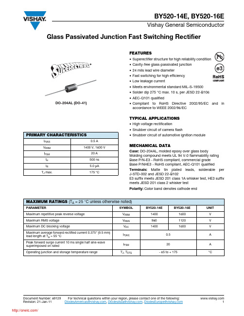
Document Number: 89129For technical questions within your region, please contact one of the following:Glass Passivated Junction Fast Switching RectifierBY520-14E, BY520-16EVishay General SemiconductorFEATURES•Superectifier structure for high reliability condition •Cavity-free glass-passivated junction •24 mils lead wire diameter •Fast switching for high efficiency •Low leakage current•Meets environmental standard MIL-S-19500•Solder dip 275 °C max. 10 s, per JESD 22-B106•AEC-Q101 qualified•Compliant to RoHS Directive 2002/95/EC and in accordance to WEEE 2002/96/ECTYPICAL APPLICATIONS•High voltage rectification •Snubber circuit of camera flash•Snubber circuit of automotive ignition moduleMECHANICAL DATACase: DO-204AL, molded epoxy over glass bodyMolding compound meets UL 94 V-0 flammability rating Base P/N-E3 - RoHS compliant, commercial grade Base P/NHE3 - RoHS compliant, AEC-Q101 qualified Terminals: Matte tin plated leads, solderable per J-STD-002 and JESD 22-B102E3 suffix meets JESD 201 class 1A whisker test, HE3 suffix meets JESD 201 class 2 whisker test Polarity: Color band denotes cathode endPRIMARY CHARACTERISTICSI F(AV)0.5 A V RRM 1400 V, 1600 VI FSM 20 A t rr 500 ns I R 5.0 μA T J max.175 °CDO-204AL (DO-41)MAXIMUM RATINGS (T A = 25°C unless otherwise noted)PARAMETERSYMBOL BY520-14EBY520-16EUNIT Maximum repetitive peak reverse voltage V RRM 14001600V Maximum RMS voltage V RMS 9801120V Maximum DC blocking voltageV DC 14001600V Maximum average forward rectified current 0.375" (9.5 mm) lead length at T A = 55 °CI F(AV)0.5A Peak forward surge current 10 ms single half sine-wave superimposed on ratedI FSM 20A Operating junction and storage temperature rangeT J , T STG- 65 to + 175°C For technical questions within your region, please contact one of the following:Document Number: 89129BY520-14E, BY520-16EVishay General SemiconductorNotes(1)Pulse test: 300 μs pulse width, 1 % duty cycle (2)Pulse test: Pulse width ≤ 40 msNote(1)Thermal resistance from junction to ambient and from junction to lead at 0.375" (9.5 mm) lead length, P.C.B. mountedNote(1)AEC-Q101 qualifiedRATINGS AND CHARACTERISTICS CURVES(T A = 25 °C unless otherwise noted)Fig. 1 - Forward Current Derating Curve Fig. 2 - Typical Instantaneous Forward CharacteristicsELECTRICAL CHARACTERISTICS (T A = 25°C unless otherwise noted)PARAMETER TE S T CONDITION S S YMBOL BY520-14EBY520-16EUNIT Maximum instantaneous forward voltageI F = 0.5 A T A = 25 °C V F (1) 2.4V Maximum reverse current V R = V RRMT A = 25 °C I R (2) 5.0μA T A = 125 °C50Maximum reverse recovery timeI F = 0.5 A, I R = 1.0 A,I rr = 0.25 At rr500nsTHERMAL CHARACTERISTICS (T A = 25°C unless otherwise noted)PARAMETERSYMBOL BY520-14EBY520-16EUNIT Typical thermal resistanceR θJA (1)65°C/WR θJL(1)30ORDERING INFORMATION (Example)PREFERRED P/N UNIT WEIGHT (g)PREFERRED PACKAGE CODEBASE QUANTITYDELIVERY MODEBY520-14E-E3/540.2454550013" diameter paper tape and reel BY520-14EHE3/54 (1)0.2454550013" diameter paper tape and reelDocument Number: 89129For technical questions within your region, please contact one of the following:BY520-14E, BY520-16EVishay General SemiconductorFig. 3 - Typical Reverse Characteristics Fig. 4 - Typical Junction CapacitancePACKAGE OUTLINE DIMENSIONS in inches (millimeters)Legal Disclaimer Notice VishayDisclaimerALL PRODU CT, PRODU CT SPECIFICATIONS AND DATA ARE SU BJECT TO CHANGE WITHOU T NOTICE TO IMPROVE RELIABILITY, FUNCTION OR DESIGN OR OTHERWISE.Vishay Intertechnology, Inc., its affiliates, agents, and employees, and all persons acting on its or their behalf (collectively,“Vishay”), disclaim any and all liability for any errors, inaccuracies or incompleteness contained in any datasheet or in any other disclosure relating to any product.Vishay makes no warranty, representation or guarantee regarding the suitability of the products for any particular purpose or the continuing production of any product. To the maximum extent permitted by applicable law, Vishay disclaims (i) any and all liability arising out of the application or use of any product, (ii) any and all liability, including without limitation special, consequential or incidental damages, and (iii) any and all implied warranties, including warranties of fitness for particular purpose, non-infringement and merchantability.Statements regarding the suitability of products for certain types of applications are based on Vishay’s knowledge of typical requirements that are often placed on Vishay products in generic applications. Such statements are not binding statements about the suitability of products for a particular application. It is the customer’s responsibility to validate that a particular product with the properties described in the product specification is suitable for use in a particular application. Parameters provided in datasheets and/or specifications may vary in different applications and performance may vary over time. All operating parameters, including typical parameters, must be validated for each customer application by the customer’s technical experts. Product specifications do not expand or otherwise modify Vishay’s terms and conditions of purchase, including but not limited to the warranty expressed therein.Except as expressly indicated in writing, Vishay products are not designed for use in medical, life-saving, or life-sustaining applications or for any other application in which the failure of the Vishay product could result in personal injury or death. Customers using or selling Vishay products not expressly indicated for use in such applications do so at their own risk and agree to fully indemnify and hold Vishay and its distributors harmless from and against any and all claims, liabilities, expenses and damages arising or resulting in connection with such use or sale, including attorneys fees, even if such claim alleges that Vishay or its distributor was negligent regarding the design or manufacture of the part. Please contact authorized Vishay personnel to obtain written terms and conditions regarding products designed for such applications.No license, express or implied, by estoppel or otherwise, to any intellectual property rights is granted by this document or by any conduct of Vishay. Product names and markings noted herein may be trademarks of their respective owners.Material Category PolicyVishay Intertechnology, Inc. hereb y certifies that all its products that are identified as RoHS-Compliant fulfill the definitions and restrictions defined under Directive 2011/65/EU of The European Parliament and of the Council of June 8, 2011 on the restriction of the use of certain hazardous substances in electrical and electronic equipment (EEE) - recast, unless otherwise specified as non-compliant.Please note that some Vishay documentation may still make reference to RoHS Directive 2002/95/EC. We confirm that all the products identified as being compliant to Directive 2002/95/EC conform to Directive 2011/65/EU.Revision: 12-Mar-121Document Number: 91000分销商库存信息:VISHAY-GENERAL-SEMICONDUCTORBY520-14E-E3/54BY520-16E-E3/54BY520-14EHE3/54 BY520-16EHE3/54。
DC1C-A1AA;DC3C-A1LB;DC2CA1RB;DC2C-AWAA;DC3C-A1AA;中文规格书,Datasheet资料
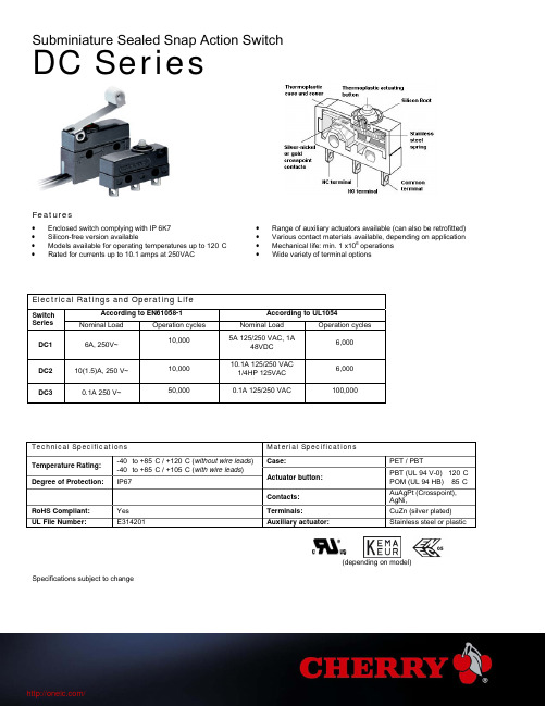
DC Series
Ordering Information
/
Contact
Call, fax or visit our Website for more information.
ZF Electronics Corporation 11200 88th Avenue Pleasant Prairie, WI 53158
Hole pattern for pcb terminals with location pins
(Post Dimensions)
Hole pattern for pcb terminals without location pins
/
Subminiature Sealed Snap Action Switch
DC Series
Terminal Options inches (mm)
Hole pattern for .051” (1.3) pcb
Short Solder Code A
0.110 x 0.020 QC (2.8 x 0.5)
Code L
0.051 X 0.020 PCB Code H (1.3 x 0.5)
6,000
0.1A 125/250 VAC
100,000
Technical Specifications
MU11-4201中文资料
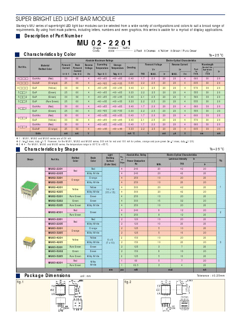
De s c ription of Pa rt NumberS t a n l e y ’s MU series of super-bright LED light bar modules can be selected from a wide variety of configurations and colors to suit a broad range ofre q u i rements. By using front mask patterns, including letters, numbers and even graphics, this series is usable for a myriad of display applications.C h a r a c t e ristics by ColorC h a r a c t e ristics by Shap ePa ckage Dimensionsunit : mmT olerance : ±0.25mmfig.1fig.2Ch ara c teristics by Shap ePa ckage Dimensions unit : mm T olerance : ±0.25mm fig.3fig.4fig.5fig.6fig.7MU04-2101MU04-2105MU04-3101MU04-3105MU04-4101MU04-4105MU04-5101MU04-5102MU04-5105MU07-2101MU07-4101MU07-5101MU08-2201MU08-3201MU08-4201MU08-5201MU08-9301UnitsMU07-31014206x19(7x20)202020202020202020202020202020202020mA3232161632321620164020402040204020121215158815158108201020102010201088mcd180180190190225225190225190300320375320240250300250240250mW3333333335555444444pcsRedMilky WhiteOrangeMilky WhiteYellowMilky WhiteGreenGreenMilky WhiteYellowGreenRedOrangeYellowGreenGreenmmRedOrangeYellowPure GreenGreenPure GreenRedOrangeRedPure GreenY ellowPure GreenRedOrangeY ellowPure GreenRedOrange6x29(7x30)14x16(15x17)567 Shape Part No.EmittedColorResinColorLightEmittingSurface(Outer Size)N o.o fC h i p sAbsolute Max. RatingPower DissipationPdElectro-Optical CharacteristicsLuminous Intensity IvMIN.TYP.I Ffig.T a=25°CCh a r a cte ristics by ShapePa ckage Dimensionsunit : mmfig.8fig.9fig.10fig.11Absolute Max. Rating Power DissipationPdElectro-Optical Characteristics Luminous Intensity Iv MIN.TYP .I F fig.ShapePart No.Emitted Color Resin ColorLight Emitting Surface (Outer Size)No.of Chips MU09-9101MU09-9102MU09-9103MU11-2201MU11-3201MU11-4201MU11-5201MU13-9102Units820φ6.4(φ7)20202020202020202020202020202020202086812882010201012141240161612121644464410510567620886686012560150601251201251501256031060375120120125125150mW1212122222151522222pcsMilky WhiteMilky WhiteMilky WhiteRed Orange Yellow Milky WhiteRed Milky White Orange Milky White mmRed Orange Y ellow Pure GreenRed YellowPure GreenPure GreenRed Yellow RedOrangeGreen Milky White4.6x 9.5(5.6x 10.5)4x 12(5x 13)101112MU17-2101MU17-2105MU17-3101MU17-3105MU17-4101MU17-4105MU17-5101MU17-5105MU16-2101MU16-2105MU16-3101MU16-3105MU16-4101MU16-4105MU16-5101MU16-5105YellowPure GreenRedOrangeMU13-9101Red Pure GreenRed Yellow Red Orange Yellow Milky White Green Milky WhiteRed Milky White Orange Milky White Y ellow Milky White Green Milky White9x 9(10.1x 10.1)4x 19(5x 20)2333333332215012512518018019019022522519019084412129912125516882424181824241010mcdmA20202020202020202020209Ta=25°CT olerance : ±0.25mmCh a r act e ristics by ShapePa ckage Dimensionsunit : mmT olerance : ±0.25mmfig.12fig.13fig.14fig.15fig.16Absolute Max. Rating Power DissipationPdElectro-Optical Characteristics Luminous Intensity Iv MIN.TYP .I F fig.ShapePart No.Emitted ColorResin Color Light Emitting Surface (Outer Size)No.of Chips MU20-2101MU20-2105MU20-3101MU20-3105MU20-4101MU20-4105MU20-5101MU20-5105MU91-2001MU91-3001MU91-5001MU92-2001MU92-3001MU92-4001MU92-5001MU93-2001MU93-300113205x 9(6x 10)20202020202020202020202020202020202020886688446662.46662.4888443344223331.23331.2444606062.5062.50757562.5062.5060757575607575756075757511111111111111111111Red Milky White Orange Milky WhiteYellow Milky White Green Milky WhiteRed Green Red Orange Y ellow Green mm RedOrangeY ellowPure GreenRed Orange Y ellow Pure GreenOrange Y ellow 6x 6(6x 6)9x 5(9x 5)141516mApcsmW1.5310x 10(10x 10)Red Orange Yellow GreenUnitsRed Orange Y ellow Pure GreenRed Orange Y ellow Pure GreenMU93-4001MU93-5001MU91-4001mcdTa=25°C。
MSK4201中文资料

PWM INPUT - Is a TTL compatible input pin for providing the PWM signal to modulate the output switches. The duty cycle can be between 0% (DC Low) and 100% (DC High). See typical system operation notes.
(315) 701-6751
FEATURES:
Low Cost Complete H-Bridge 28 Volt, 5 Amp Capability, 75 Volt Maximum Rating Self-contained Smart Lowside/Highside Drive Circuitry Internal Deadtime Generation, Shoot-through Protection Output Disable/Shutdown Capability Isolated Case Allows Direct Heatsinking Four Quadrant Operation, Torque Control Capability Available Fully Screened To MIL-H-38534
Peak Output Current 37A ○
○
○
○
○
○
○
○
○
○
○
○
○
○
○
Output Voltage Range GND-2V min. To V+ max.
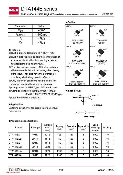
DTA144EUBTL;中文规格书,Datasheet资料
OUTPUT CURRENT : IO [A]
© 2012 ROHM Co., Ltd. All rights reserved.
3/10
2012.04 - Rev.A
/
DTA144E series
lElectrical characteristic curves(Ta = 25°C)
4/10
2012.04 - Rev.A
/
DTA144E series
lDimensions (Unit : mm)
D b1 c
Data Sheet
VMT3
A
L
e
b
H
E
x
S A b3
l1
Lp
A
A1
S
l1
b2
e
Patterm of terminal position areas
DTA144E series
PNP -100mA -50V Digital Transistors
(Bias Resistor Built-in Transistors)
Datasheet
lOutline Parameter Value
VMT3 OUT IN GND IN GND EMT3F OUT
Data Sheet
Symbol VCC VIN IO IC(MAX.)*1
MIC5841YWM TR;MIC5841YWM;MIC5841YN;MIC5841YV;MIC5842YN;中文规格书,Datasheet资料

MIC5841/58428-Bit Serial-Input Latched DriversMicrel Inc. • 2180 Fortune Drive • San Jose, CA 95131 • USA • tel +1 (408) 944-0800 • fax + 1 (408) 474-1000 • General DescriptionUsing BiCMOS technology, the MIC5841/5842 integrated circuits were fabricated to be used in a wide variety of peripheral power driver applications. The devices each have an eight-bit CMOS shift register, CMOS control circuitry, eight CMOS data latches, and eight bipolar current-sink Darlington output drivers.These two devices differ only in maximum voltage ratings. The MIC5842 offers premium performance with a minimum output breakdown voltage rating of 80V (50Vsustaining). The drivers can be operated with a split supplywhere the negative supply is down to –20V.The 500mA outputs, with integral transient-suppressiondiodes, are suitable for use with lamps, relays, solenoids and other inductive loads.These devices have improved speed characteristics. With a 5V logic supply, they will typically operate faster than 5 MHz. With a 12V supply, significantly higher speeds are obtained. The CMOS inputs are compatible with standard CMOS, PMOS, and NMOS logic levels. TTL or DTL circuits may require the use of appropriate pull-up resistors. By using the serial data output, the drivers can be cascaded for interface applications requiring additional drive lines.The MIC5840 family is available in DIP, PLCC, and SOIC packages. Because of limitations on package power dissipation, the simultaneous operation of all drivers at maximum rated current might require a reduction in duty cycle. A copper-alloy lead frame provides for maximum package power dissipation.Features• 3.3 MHz Minimum Data-Input Rate • CMOS, PMOS, NMOS, TTL Compatible• Internal Pull-Up/Pull-Down Resistors • Low-Power CMOS Logic and Latches• High-Voltage Current-Sink Outputs• Output Transient-Protection Diodes • Single or Split Supply OperationOrdering InformationPart NumberStandard Pb-Free Temperature RangePackage MIC5841BN MIC5841YN –40ºC to +85ºC 18-Pin Plastic DIP MIC5841BV MIC5841YV –40ºC to +85ºC 20-Pin PLCC MIC5841BWM MIC5841YWM –40ºC to +85ºC 18-Pin Wide SOIC MIC5842BN MIC5842YN –40ºC to +85ºC 18-Pin Plastic DIP MIC5842BV MIC5842YV –40ºC to +85ºC 20-Pin PLCC MIC5842BWM MIC5842YWM–40ºC to +85ºC18-Pin Wide SOICFunctional DiagramSERIAL DATA OUT CLKV S SV DDS T R O B EOUTPUT ENABLE (ACTIVE LOW)87654321Absolute Maximum Ratings (1,2,3)At 25°C Free-Air Temperature and V SS ...................0V Output Voltage, V CE (MIC5841)............................. 50V (MIC5842)..............................80V Output Voltage, V CE(SUS) (MIC5841)(1)..................................35V (MIC5842)........................50V Logic Supply Voltage, V DD .......................................15V VDD with Reference to V EE . (25V)Emitter Supply Voltage, V EE ...................................–20V Input Voltage Range, V IN ...............–0.3V to V DD + 0.3V Continuous Output Current, I OUT .........................500mA Package Power Dissipation, P D (2)........................1.82W Operating Temperature Range, T A .......–55°C to +85°C Storage Temperature Range, T S ........–65°C to +150°CElectrical CharacteristicsAt T A = 25°C V DD = 5V, V SS = V EE = 0V (unless otherwise noted)LimitsCharacteristic Symbol Applicable Devices Test ConditionsMin Max Unit V OUT = 50V50 MIC5841V OUT = 50V, T A = +70ºC100 V OUT = 80V50 Output Leakage CurrentI CEXMIC5842 V OUT = 80V, T A = +70ºC100 µAI OUT = 100mA1.1 I OUT = 200mA1.3 Collector-Emitter Saturation VoltageV CE(SAT) Both I OUT = 350mA, V DD = 7.0V1.6V MIC5841 I OUT = 350mA, L = 2mH35Collector-Emitter Saturation Voltage V CE(SUS)(5)MIC5842 I OUT = 350mA, L = 2mH50V V IN(0) Both0.8V DD = 12V 10.5 V DD = 10V 8.5 Input VoltageV IN(1) BothV DD = 5.0V(4)3.5 V V DD = 12V50 V DD = 10V 50 Input ResistanceR IN Both V DD = 5.0V50k Ω All Drivers ON, V DD = 12V16All Drivers ON, V DD = 10V 14 IDD (ON) Both All Drivers ON, V DD = 5.0V 8.0 All Drivers OFF, V DD = 12V 2.9 All Drivers OFF, V DD = 10V 2.5 Supply CurrentIDD (OFF) BothAll Drivers OFF, V DD = 5.0V1.6 1.6 MIC5841 V R = 50V50 Clamp Diode Leakage Current I R MIC5842 V R = 80V50 µA Clamp Diode Forward VoltageV F Both I F = 350mA2.0 VElectrical CharacteristicsAt T A = –55°C V DD = 5V, V SS = V EE = 0V (unless otherwise noted)LimitsCharacteristic Symbol Test Conditions Min Max Unit Output Leakage CurrentI CEX V OUT = 80V 50 µA I OUT = 100mA 1.3 I OUT = 200mA1.5 Collector-Emitter Saturation VoltageV CE(SAT)I OUT = 350mA, V DD = 7.0V1.8 V V IN(0)0.8 V DD = 12V 10.5 Input VoltageV IN(1)V DD = 5.0V3.5 V V DD = 12V35 V DD = 10V 35 Input ResistanceR IN V DD = 5.0V35k Ω All Drivers ON, V DD = 12V16All Drivers ON, V DD = 10V 14 I DD(ON) All Drivers ON, V DD = 5.0V10 All Drivers OFF, V DD = 12V3.5 Supply CurrentI DD(OFF) All Drivers OFF, V DD = 5.0V2.0mAElectrical CharacteristicsAt T A = +125°C V DD = 5V, V SS = V EE = 0V (unless otherwise noted)LimitsCharacteristic Symbol Test Conditions Min Max Unit Output Leakage CurrentI CEX V OUT = 80V 500 µA I OUT = 100mA 1.3 I OUT = 200mA1.5 Collector-Emitter Saturation VoltageV CE(SAT)I OUT = 350mA, V DD = 7.0V1.8 V V IN(0)0.8 V DD = 12V 10.5 Input VoltageV IN(1)V DD = 5.0V3.5 V V DD = 12V50 V DD = 10V 50 Input ResistanceR IN V DD = 5.0V50 k Ω All Drivers ON, V DD = 12V16 All Drivers ON, V DD = 10V 14 I DD(ON) All Drivers ON, V DD = 5.0V 8 All Drivers OFF, V DD = 12V 2.9 Supply CurrentI DD(OFF)All Drivers OFF, V DD = 5.0V2.1.6 mA MIC5841A V R = 50V1.6 µA Clamp Diode Leakage CurrentI R MIC5842A V R = 80V100Notes :1. For Inductive load applications.2. Derate at the rate of 18.2mW/°C above TA = 25°C (Plastic DIP)3. CMOS devices have input-static protection but are susceptible to damage when exposed to extremely high static electrical charges.4. Operation of these devices with standard TTL may require the use of appropriate pull-up resistors to insure an input logic HIGH.5. Not 100% tested. Guaranteed by design.Timing Conditions(TA = 25°C Logic Levels are V DD and V SS ) V DD = 5V A. Minimum Data Active Time Before Clock Pulse (Data Set-Up Time)...................................................................... 75 ns B. Minimum Data Active Time After Clock Pulse (Data Hold Time) ............................................................................75 ns C. Minimum Data Pulse Width ...................................................................................................................................150 ns D. Minimum Clock Pulse Width...................................................................................................................................150 ns E. Minimum Time Between Clock Activation and Strobe ...........................................................................................300 ns F. Minimum Strobe Pulse Width..................................................................................................................................100 ns G. Typical Time Between Strobe Activation and Output Transition............................................................................500 ns SERIAL DATA present at the input is transferred to the shift register on the logic “0” to logic “1” transition of the CLOCK input pulse. On succeeding CLOCK pulses, the registers shift data information towards the SERIAL DATA OUTPUT. The SERIAL DATA must appear at the input prior to the rising edge of the CLOCK input waveform.Information present at any register is transferred to its respective latch when the STROBE is high (serial-to-parallel conversion). The latches will continue to accept new data as long as the STROBE is held high. Applications where the latches are bypassed (STROBE tied high) will require that the ENABLE input be high during serial data entry. When the ENABLE input is high, all of the output buffers are disabled (OFF) without affecting information stored in the latches or shift register. With the ENABLE input low, the outputs are controlled by the state of the latches.MIC5840 Family Truth TableShift Register Contents Latch Contents Output Contents Serial Data InputClock InputI 1I 2I 3 … I 8Serial Data OutputStrobe InputI 1I 2I 3 … I 8 OutputEnableI 1I 2I 3…I 8H H R1 R2 … R7 R7 L L R1 R2 … R7 R7 X R1 R2 R3 … R8 R8X X X … X X L R1 R2 R3 … R8P1 P2 P3 … P8P8 H P1 P2 P3 … P8 L P1 P2 P3 …P8X X X (X)HH H H …HL = Low Logic Level H = High Logic Level X = Irrelevant P = Present State R = Previous StateTypical Output DriverTypical Input CircuitsMaximum Allowable Duty Cycle (Plastic DIP)V DD = 5.0VMax. Allowable Duty Cycle at Ambient Temperature ofNumber of Outputs ON(I OUT = 200mA V DD = 5.0V)25ºC 40ºC 50ºC 60ºC 70ºC8 85% 72% 64% 55% 46%7 97% 82% 73% 63% 53% 6 100% 96% 85% 73% 62%5 100% 100% 100% 88% 75% 4 100% 100% 100% 100% 93%3 100% 100% 100% 100% 100%2 100% 100% 100% 100% 100%1100% 100% 100% 100% 100%V DD = 12VMax. Allowable Duty Cycle at Ambient Temperature ofNumber of Outputs ON(I OUT = 200mA V DD = 12V)25ºC 40ºC 50ºC 60ºC 70ºC8 80% 68% 60% 52% 44%7 91% 77% 68% 59% 50%6 100% 90% 79% 69% 58% 5 100% 100% 95% 82% 69%4 100% 100% 100% 100% 86%3 100% 100% 100% 100% 100%2 100% 100% 100% 100% 100%1100% 100% 100% 100% 100%Typical ApplicationsRelay/Solenoid Driver MIC5842 MIC5841 Hammer DriverMIC5841 Solenoid Driver with Output Enable MIC5841 Level Shifting Lamp Driver withDarlington Emitters Tied to a Negative SupplyTypical Applications, ContinuedMICREL, INC. 2180 FORTUNE DRIVE SAN JOSE, CA 95131 USATEL +1 (408) 944-0800 FAX +1 (408) 474-1000 WEB http:/The information furnished by Micrel in this data sheet is believed to be accurate and reliable. However, no responsibility is assumed by Micrel for its use. Micrel reserves the right to change circuitry and specifications at any time without notification to the customer.Micrel Products are not designed or authorized for use as components in life support appliances, devices or systems where malfunction of a product can reasonably be expected to result in personal injury. Life support devices or systems are devices or systems that (a) are intended for surgical implant into the body or (b) support or sustain life, and whose failure to perform can be reasonably expected to result in a significant injury to the user. A Purchaser’s use or sale of Micrel Products for use in life support appliances, devices or systems is a Purchaser’s own risk and Purchaser agrees to fullyindemnify Micrel for any damages resulting from such use or sale.© 1998 Micrel, Incorporated.分销商库存信息:MICRELMIC5841YWM TR MIC5841YWM MIC5841YNMIC5841YV MIC5842YN MIC5842YWM MIC5842YV MIC5841YV TR MIC5842YWM TR MIC5842YV TR MIC5841BN MIC5841BWM MIC5841BWM TR MIC5842BN MIC5841BVMIC5841BV TR MIC5842BV MIC5842BV TR MIC5842BWM MIC5842BWMTR。
LTC4411ES5#TRMPBF;LTC4411ES5#TR;LTC4411ES5#TRPBF;LTC4411ES5#TRM;中文规格书,Datasheet资料

IFWD
Figure 1. Automatic Switchover of Load Between a Battery and a Wall Adapter
VFWD
/
U
LTC4411 vs Schottky Diode Forward Voltage Characteristics
LTC4411 2.6A Low Loss Ideal Diode in ThinSOTTM
FEATURES
■ ■ ■ ■ ■ ■ ■ ■ ■ ■ ■ ■
ቤተ መጻሕፍቲ ባይዱ
DESCRIPTIO
Low Loss Replacement for PowerPathTM OR’ing Diodes Small Regulated Forward Voltage (28mV) 2.6A Maximum Forward Current Low Forward ON Resistance (140mΩ Max) Low Reverse Leakage Current (<1µA) 2.6V to 5.5V Operating Range Internal Current Limit Protection Internal Thermal Protection No External Active Components Pin-Compatible Monolithic Replacement for the LTC4412 Low Quiescent Current (40µA) Low-Profile (1mm) 5-lead SOT-23 Package
●
ELECTRICAL CHARACTERISTICS
STAT Output IS(SNK) IS(OFF) tS(ON) tS(OFF) CTL Input VTH VHYST ICTL IOC IQOC
TPL0401EVM;中文规格书,Datasheet资料

User's GuideSLIU008–September2011TPL0401EVMContents1Features (2)2Introduction (2)3Mode Selection (2)4Jumpers Connections (3)5Software Setup (3)6Schematics,Layout and Bill of Materials (6)List of Figures1GUI for DPOT Control (4)2TPL0401B Variable Gain (5)3TCA5405,TCA7408Schematic (6)4TLC59108Schematic (7)5TPL0401Schematic (7)6Routing,Assembly and Silkscreen Top (9)7Layer2Power Plane (10)8Layer3Ground Plane (11)9Routing and Assembly Bottom (12)List of Tables1Description of Connectors and Jumpers (3)2430Boost-TPL0401EVM Bill of Material (12)Windows is a trademark of Microsoft Corporation.1 SLIU008–September2011TPL0401EVMSubmit Documentation FeedbackCopyright©2011,Texas Instruments Incorporated/Features 1Features•Works with low cost MSP430based LaunchPad platform•Simple GUI to control EVM•EVM can be operated in three different modes–Auto run LED mode–Adjustable Voltage reference mode–Variable gain mode•Board is powered by USB2IntroductionThe TPL0401is an I2C bus controlled,single channel,linear-taper digital potentiometer with128wiperpositions.TPL0401A/B have an end-to-end resistance of10k ohms and the low terminal internallyconnected to ground.The position of the wiper can be adjusted using an I2C interface.The TPL0401isavailable in a6-pin SC-70package with a specified temperature range of–40°C to125°C.The part has a10k end-to-end resistance and can operate with a supply voltage range of2.7V to5.5V.THE TPL0401EVM also consists of multiple other TI products(port expanders,LED drivers etc.).However,the scope of this document is to illustrate the use of the EVM to evaluate the TPL0401.TheTPL0401EVM is designed to operate with the Texas Instruments LaunchPad(MSP-EXP430G2).TheTPL0401EVM comes with a preprogrammed MSP430G2553microcontroller which is to be inserted in theDIP socket on the LaunchPad.The LaunchPad can be separately purchased at /launchpad.The TPL0401EVM has three different evaluation modes:Mode1–LED mode–This is the standard mode the TPL0401comes up in when powered up.In thismode the TPL0401devices are used to control the color mixing on the RGB LEDs.The DPOTs are usedto set the current limit for the TLC59108LED driver.This mode is and auto run mode that does not haveany GUI control.The flashing lights and color mixing is controlled by the keys on the board and other TIproducts on the board.Mode2–Adjustable voltage reference mode–in this mode the TPL0401is used in conjunction with anLMV321op amp as an adjustable voltage reference circuit.Mode3–Variable gain mode–in this mode the TPL0401is configured as part of a variable gainnon-inverting amplifier.The gain of the amplifier can be controlled by a digital interface.This mode can beused to evaluate the bandwidth of the TPL0501.The EVM is operated by connecting the LaunchPad to a PC that has Windows™()via the USBPort.Other standard lab equipment such as Signal generator,multimeter,spectrum analyzer etc may berequired for detailed analysis of the TPL0501performance using this EVM.3Mode SelectionTo setup any of these two modes,begin by connecting the EVM to the LaunchPad.Note the location ofthe VCC and GND pins on headers J1and J2on both the LaunchPad and the EVM to ensure correctinstallation.1.LED ModeConnect Jumpers1and2of J6Connect+5V supply to J3Connect LaunchPad to computer through USB cableNOTE:It can be possible to power up the LEDs by connecting a wire from the VCC pin of J1to thepositive pin of J3.A5V supply might be required because the max voltage drop across the blue LEDplus the drop across the TLC59108is larger than the supply voltage of the LaunchPad.2.Voltage reference modeStart up the board in LED mode as described earlierConnect pins1and2of Jumper J7.Connect pins1and2of Jumper J5.Connect the LaunchPad and TPL0501EVM to a computer through the USB connector.2TPL0401EVM SLIU008–September2011Submit Documentation FeedbackCopyright©2011,Texas Instruments Incorporated/ Jumpers Connections Press keys SW2and SW3simultaneouslyStart GUI software on computer3.Variable Gain modeConnect pins2and3of jumper J6.Connect pins1and2of jumper J7.Attach a signal generator to the EXT_IN connector(SMA or SMB connector may need to bepopulated).Press keys SW2and SW3simultaneouslyStart GUI software on computerConnect the LaunchPad and TPL0501EVM to a computer through the USB connector4Jumpers Connections1.J1&J2–LaunchPad HeadersThese connectors mate with the male headers on the LaunchPad2.J3–External LED PowerThis connector is where the external+5V supply is attached to power the two RGB LEDs.3.J4–TCA7408GPIOThis is a pin out of the four unused GPIO pins from the TCA7408,GPIO4-GPIO7.4.J5–Feedback loopFor the TPL0401A to function as a voltage reference circuit the negative feedback loop must beshorted,placing a jumper across this header will short the inverting input to the output.5.J6–LED or Op-ampThis header controls what the TPL0401B is attached to.When shorted across position1and2theTPL0401B is connected in series with the external resistor to control the current through the LEDdriver.When shorted across position2and3the TPL0401B is connected to the inverting input of theop-amp to change the gain of the circuit.6.J7–Op-amp inputThis header controls the input to the non-inverting pin of the LMV321.When shorted across position1and2,the TPL0401A in a voltage divider mode is attached to the non-inverting input of the LVM321.This setup is used to test the voltage reference setup.When shorted across pins2and3,the SMAconnector is attached to the non-inverting input.7.J9–Test PointsThis connector offers test points for the serial data lines,SDA,SCL and the DIN that drives theTCA5405Table1.Description of Connectors and JumpersLabel DescriptionJ1,J2Connectors to interface with LaunchPadJ3External5V for LEDJ4GPIO4-GPIO7from TCA7408J5Control jumper to short feedback loopJ6Jumper to control LED or Op-AmpJ7Jumper to control input to Op-AmpJ8SMA/B Footprint for external inputJ9Test points for DIN,SDA and SCL5Software SetupThe EVM does not require any software set up to operate in the LED mode.The keys SW1-SW4controlthe blinking rate of the LEDs and the color mixing of the LEDs,without any additional software setup.To operate the EVM in any other mode,GUI software is required.The GUI software is available in a zip3 SLIU008–September2011TPL0401EVMSubmit Documentation FeedbackCopyright©2011,Texas Instruments Incorporated/Software Setup file located on the TPL0401product page on .Download the zip file and extract its contents toa desired location on your PC.You will see an executable file called TPL0401_GUI.exe in the extractedfolder.Double click the file to open it and the GUI program should launch.IMPORTANT:Before launchingthe GUI please make sure the TPL0401EVM is setup in the desired mode and connected to the PCthrough a USB port.Figure1.GUI for DPOT ControlThere are three methods to adjust the value of the TPL0401A/B.Start by clicking one of the buttonscircled in GREEN to select the corresponding TPL0401device.To adjust the tap value directly simply click the box that says tap and you will be prompted to input a tapvalue between0and127.After typing in the desired value press enter and the tap value will be sent tothe TPL0401A and the GUI will reflect the value you just entered.To adjust the TPL0401by inputting a wiper to low terminal resistance,click the box that says W-LResistance.You will then be prompted to input a value between0and10,000ohms;press enter after youhave input a value.The GUI will use the theoretical resistance values to find a tap that is closest to thevalue that was input.NOTE:All W-L resistance values are typical values;the actual value will be within20%of thedisplayed value4TPL0401EVM SLIU008–September2011Submit Documentation FeedbackCopyright©2011,Texas Instruments Incorporated/OUT Software Setup5.1Voltage Reference ModeMake sure the EVM is set up in voltage reference mode as described in Section 3.With the GUI open and TPL0401A selected you are also given the option to change the voltage divider ratio of the TPL0401A as a percent value.To do this simply click the box that says percent and you will be prompted to input apercent value between 0and 100;decimal values can be used.After pressing enter,the GUI will find and send the tap value that is closest to the chosen percent value.Using any of the methods to change the tap value of the TPL0401A will update the output voltage at TP1.The output will be a percent of the supply voltage,3.6V.5.2Variable Gain ModeThe 430Boost-TPL0401EVM allows for a variable gain setup to evaluate the bandwidth of the TPL0401.After following the setup instructions in section 2.3.2?,the circuit will look as follows:Figure 2.TPL0401B Variable GainThe capacitor C6and the resistor R12are unpopulated and should be set by the user.R12will set the possible gain values and C6will keep the loop stable.Changing the value of the TPL0401B works the same as described in the beginning of section 3.1.5SLIU008–September 2011TPL0401EVMSubmit Documentation FeedbackCopyright ©2011,Texas Instruments Incorporated/Schematics,Layout and Bill of Materials6Schematics,Layout and Bill of Materials6.1SchematicsFigure3.TCA5405,TCA7408Schematic6TPL0401EVMCopyright©2011,Texas Instruments Incorporated / SchematFigure4.TLC59108SchematicFigure5.TPL0401SchematicSLIU008–September2011Submit Documentation FeedbackCopyright©2011,Texas Instruments Incorporated/Schematics,Layout and Bill of Materials8TPL0401EVMCopyright©2011,Texas Instruments Incorporated / Schematics,Layout and Bill of Materials6.2LayoutsFigure6.Routing,Assembly and Silkscreen Top9 SLIU008–September2011TPL0401EVMSubmit Documentation FeedbackCopyright©2011,Texas Instruments Incorporated/Schematics,Layout and Bill of Materials yer2Power Plane10TPL0401EVM SLIU008–September2011Submit Documentation FeedbackCopyright©2011,Texas Instruments Incorporated/分销商库存信息: TITPL0401EVM。
MAX4204EUA+中文资料
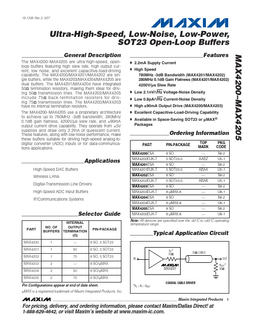
___________Typical Application Circuit
MAX4200 MAX4201 MAX4202 MAX4203 MAX4204 MAX4205
8 SO, 5 SOT23 8 SO, 5 SOT23 8 SO, 5 SOT23 8 SO/µMAX 8 SO/µMAX 8 SO/µMAX MAX4201
________________________Applications
High-Speed DAC Buffers Wireless LANs Digital-Transmission Line Drivers High-Speed ADC Input Buffers IF/Communications Systems
DC ELECTRICAL CHARACTERISTICS
(VCC = +5V, VEE = -5V, RL = ∞, TA = TMIN to TMAX, unless otherwise noted. Typical values are at TA = +25°C.) PARAMETER Operating Supply Voltage Quiescent Supply Current Input Offset Voltage Input Offset Voltage Drift Input Offset Voltage Matching Input Bias Current Input Resistance Voltage Gain Power-Supply Rejection Output Resistance IB RIN AV PSR ROUT (Note 1) -3.0V ≤ VOUT ≤ 3.0V MAX4200/MAX4203, REXT = 150Ω MAX4201/MAX4204, REXT = 50Ω MAX4202/MAX4205, REXT = 75Ω MAX4200/MAX4203 f = DC MAX4201/MAX4204 MAX4202/MAX4205 MAX4200/MAX4203 Output Current IOUT RL = 30Ω MAX4201/MAX4204 MAX4202/MAX4205 MAX4200/MAX4203 Short-Circuit Output Current ISC Sinking or sourcing MAX4201/MAX4204 MAX4202/MAX4205 RL = 150Ω MAX4200/MAX4203 Output-Voltage Swing VOUT MAX4201/MAX4204 MAX4202/MAX4205 RL = 100Ω RL = 37.5Ω RL = 50Ω RL = 75Ω ±1.9 ±2.0 ±3.3 ±3.2 0.9 0.42 0.41 55 SYMBOL VS IS VOS TCVOS CONDITIONS Guaranteed by PSR test Per buffer, VIN = 0V VIN = 0V VIN = 0V MAX4203/MAX4204/MAX4205 MIN ±4 2.2 1 20 0.4 0.8 500 0.96 0.50 0.50 72 8 50 75 ±90 ±52 ±44 150 90 75 ±3.8 ±3.7 ±3.3 ±2.1 ±2.3 V mA mA Ω 1.1 0.58 0.59 dB V/V 10 TYP MAX ±5.5 4 15 UNITS V mA mV µV/°C mV µA kΩ
TEA1721ATN1,118;中文规格书,Datasheet资料

The TEA1721 is a small and low cost module Switched Mode Power Supply (SMPS) controller IC for low power applications (up to 5 W) and operates directly from the rectified universal mains input. The device includes a high voltage power switch (700 V) and has been optimized for flyback converter topologies to provide high-efficiency over the entire load range with ultra-low power consumption in the no-load condition. It provides a circuit for start-up directly from the rectified mains voltage without any external bleeder circuits.
/
NXP Semiconductors
TEA1721AT
HV start-up flyback controller with integrated MOSFET for 5 W
Green features:
Enables no-load power consumption below < 10 mW Very low supply current in no-load condition with energy saver mode Incorporates a high voltage start-up circuit with zero current consumption under
PC4201B-12CFT中文资料
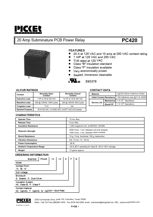
20 Amp Subminature PC B Power RelayFEATURES20 A at 125 VAC and 10 amp a t 250 VAC contact rating 1 \HP at 125 VAC and 250 VAC Class "B" insulation standard TV8 rated at 125 VACClass "F" insulation available Very economically priced PC420UL/CUR RATINGSCHARACTERISTICSOperate Time 15 ms. Max.Release Time Insulation Resistance 5 ms. Max.1,000 megohms min, at 500VDC, 50%RH Dielectric Strength 4000 Vrms, 1 min. between coil and contacts 1000 Vrms, 1 min. between open contacts Shock Resistance 10 g, 11ms, functional; 100 g, destructive Vibration Resistance DA 1.5 mm, 10 - 55 Hz Power Consumption .36 WAmbient Temperature Range -40 to 85 C operating for class B, -40 to 130 C s torage Weight13 grams approx.Sales: Call Toll Free (888)997-3933 Fax (818) 342-5296 email: pickerwest@ URL: 3220 Commander Drive, Suite 102, Carrollton, T exas 75006PC420 Rev C 4-26-05PAGE 1ORDERING INFORMATIONExample:PC420Model -1A1A, 1B, 1C Sealed, immersion cleanableSCONTACT DATAMaterialInitial Contact Resistance Service LifeMechanical ElectricalAgCdO (Silver Cadmium Oxide)100 milliohms max @ 0.1A, 6VDC 1 X 1071 X 105Operations OperationsInsulation SystemNil: Class B, F: Class FContact Form Contact MaterialNil: AgCdO, T: AgSnO, G: AgCdO + G old PlateGFCoil Voltage-1220 A/125 VAC, 10 A/250 VAC, 6 A/277 VAC All Con tacts20A @ 125VAC 100K CyclesE93379EnclosureS: Sealed; C: Dust Cover Inductive Load Normally OpenContact Contact 1 HP at 125 & 250 VAC 1/2 HP at 125 & 250 VAC Normally ClosedContact Resistive Load 20A @ 125VAC 30K CyclesTungsten Load TV-8NAGeneral PurposePC420PC420COIL DATACoil Voltage56122448Resistanceohms + 10%Must OperateVoltage Max.(VDC)Must Release Voltage Min.(VDC)Continuous Voltage Max.(VDC)257010040016006400 3.54.28.416.833.60.50.61.22.44.86.57.815.631.262.4_Sales: Call Toll Free (888) 997-3933 F ax (818) 342-5296 email: pickerwest@sbc URL: 3220 Commander Drive, Suite 102, Car rollton, Texas 75006PAGE 2Note: Custom coil voltages within the ra nges shown are available on special order.Tolerances +.010 unless otherwise notedNotes:Contact Form C shownOn Contact Forms A & B Unused Pins are Omitte d3 2.10.3 3.9Dimensions in Inches (millimet ers)Side ViewEnd ViewBottom View PC Board LayoutWiring Diagram9225 6.30.911.71510151020304050100C u r r e n t i n A m p s AC Contact Voltage.20036020Contact Derating for AC loads1020304050100DC Contact Voltage.Contact Derating for DC loads151015C u r r e n t i n A m p s204030。
MS614SE,MS518SE,MS621FE,MS920SE-FL27E,MS412FE, 规格书,Datasheet 资料
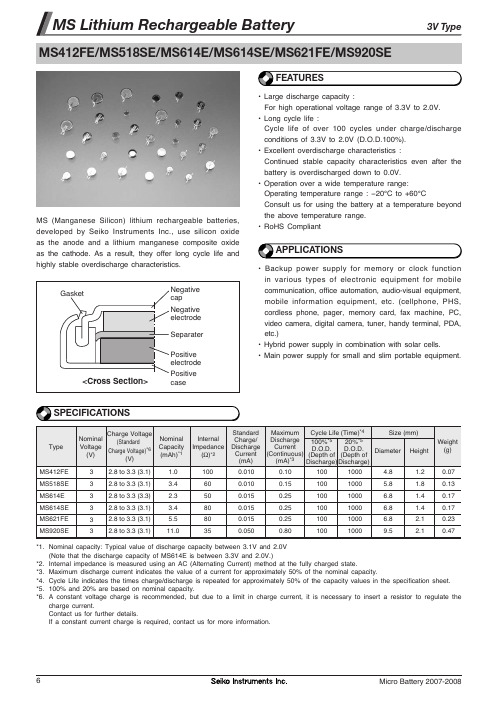
Gasket
<Cross Section>
Positive case
SPECIFICATIONS
Charge Voltage Nominal (Standard Voltage Charge Voltage)*6 (V) (V) 3 3 3 3 3 3 2.8 to 3.3 (3.1) 2.8 to 3.3 (3.1) 2.8 to 3.3 (3.3) 2.8 to 3.3 (3.1) 2.8 to 3.3 (3.1) 2.8 to 3.3 (3.1) Nominal Capacity (mAh)*1 1.0 3.4 2.3 3.4 5.5 11.0 Internal Impedance (Ω)*2 100 60 50 80 80 35 Cycle Life (Time)*4 Size (mm) Standard Maximum Charge/ Discharge 100%*5 20%*5 Discharge Current D.O.D. D.O.D. Current (Continuous) (Depth of (Depth of Diameter Height *3 (mA) (mA) Discharge) Discharge) 0.010 0.010 0.015 0.015 0.015 0.050 0.10 0.15 0.25 0.25 0.25 0.80 100 100 100 100 100 100 1000 1000 1000 1000 1000 1000 4.8 5.8 6.8 6.8 6.8 9.5 1.2 1.8 1.4 1.4 2.1 2.1 Weight (g) 0.07 0.13 0.17 0.17 0.23 0.47
ADS7828E250;ADS7828EB250;ADS7828E2K5;ADS7828E2K5G4;ADS7828EB2K5;中文规格书,Datasheet资料
Power Dissipation .................................................... (TJ max – TA)/θJA θJA Thermal Impedance ........................................................ 240°C/W Lead Temperature, Soldering
"
"
"
"
ADS7828EB/2K5 Tape and Reel, 2500
NOTE: (1) For the most current package and ordering information, see the Package Option Addendum at the end of this data sheet, or see the TI web site at .
PIN CONFIGURATION
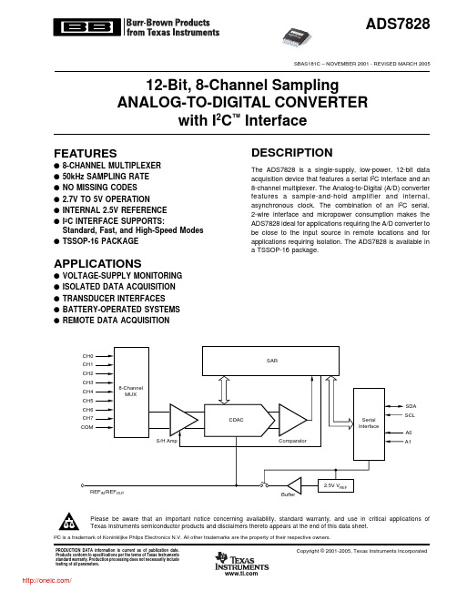
Top View
CH0 1 CH1 2 CH2 3 CH3 4 CH4 5 CH5 6 CH6 7 CH7 8
ADS7828
TSSOP
16 +VDD 15 SDA 14 SCL 13 A1 12 A0 11 COM 10 REFIN / REFOUT 9 GND
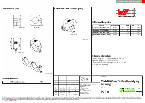
7427155;中文规格书,Datasheet资料
6.1 6.0 5.02012-06-272012-04-302007-01-25SStSStSMuSStSMu-Würth Elektronik eiSos GmbH & Co. KGEMC & Inductive SolutionsMax-Eyth-Str. 174638 WaldenburgGermanyTel. +49 (0) 79 42 945 - 0A Dimensions: [mm]Additional FeaturesSafety key to lock/ unkock74271D2 General Properties:Ferrite core Ferrite core Ferrite core Plastic housing Plastic housing Test cable Test cablePropertiesMaterial Initial permeability Curie temperatureColourFlammability ClassificationApplicable cable Applicable cable lengthµi T CValue 4 W 620620150Grey UL94-V0AWG26120Unit°Cmm Tol.typ.typ.F Typical Impedance Characteristics:I Cautions and Warnings:The following conditions apply to all goods within the product series of WE-STAR RINGof Würth Elektronik eiSos GmbH & Co. KG:General:All recommendations according to the general technical specifications of the data sheet have to be complied with.The disposal and operation of the product within ambient conditions which probably alloy or harm the component surface has to be avoided.The packaging of the product is to encase the needed humidity of the plastic housing. To ensure the humidity level, the products have to be stored in this delivered packaging. If not, the products are losing their humidity. In this case you can re-condition the components according to the internal standard WE1883 to ensure the necessary humidity in the plastic.To ensure the operating mode of the product, the ambient temperature at processing (when the part will be mounted on the cable) has to be in the range of 15 to 25 °C.Before mounting, the part should be stored for one hour in this condition.The responsibility for the applicability of customer specific products and the use in a particular customer design is always within the authority of the customer. All technical specifications for standard products do also apply for customer specific products.Direct mechanical impact to the product and the forcible closing of this shall be prevented as the ferrite material of the ferrite body or the pla-stic housing could flake or in the worst case it could break.Product specific:Follow all instructions mentioned in the datasheet, especially:•The cable diameter must be pointed out, otherwise no warranty will be sustained.•Violation of the technical product specifications such as exceeding the nominal rated current will result in the loss of warranty.1. General Customer ResponsibilitySome goods within the product range of Würth Elektronik eiSos GmbH & Co. KG contain statements regarding general suitability for certain application areas. These statements about suitability are based on our knowledge and experience of typical requirements concerning the are-as, serve as general guidance and cannot be estimated as binding statements about the suitability for a customer application. The responsibi-lity for the applicability and use in a particular customer design is always solely within the authority of the customer. Due to this fact it is up to the customer to evaluate, where appropriate to investigate and decide whether the device with the specific product characteristics described in the product specification is valid and suitable for the respective customer application or not.2. Customer Responsibility related to Specific, in particular Safety-Relevant ApplicationsIt has to be clearly pointed out that the possibility of a malfunction of electronic components or failure before the end of the usual lifetime can-not be completely eliminated in the current state of the art, even if the products are operated within the range of the specifications.In certain customer applications requiring a very high level of safety and especially in customer applications in which the malfunction or failure of an electronic component could endanger human life or health it must be ensured by most advanced technological aid of suitable design of the customer application that no injury or damage is caused to third parties in the event of malfunction or failure of an electronic component.3. Best Care and AttentionAny product-specific notes, warnings and cautions must be strictly observed.4. Customer Support for Product SpecificationsSome products within the product range may contain substances which are subject to restrictions in certain jurisdictions in order to serve spe-cific technical requirements. Necessary information is available on request. In this case the field sales engineer or the internal sales person in charge should be contacted who will be happy to support in this matter.5. Product R&DDue to constant product improvement product specifications may change from time to time. As a standard reporting procedure of the Product Change Notification (PCN) according to the JEDEC-Standard inform about minor and major changes. In case of further queries regarding the PCN, the field sales engineer or the internal sales person in charge should be contacted. The basic responsibility of the customer as per Secti-on 1 and 2 remains unaffected.6. Product Life CycleDue to technical progress and economical evaluation we also reserve the right to discontinue production and delivery of products. As a stan-dard reporting procedure of the Product Termination Notification (PTN) according to the JEDEC-Standard we will inform at an early stage about inevitable product discontinuance. According to this we cannot guarantee that all products within our product range will always be available. Therefore it needs to be verified with the field sales engineer or the internal sales person in charge about the current product availability ex-pectancy before or when the product for application design-in disposal is considered.The approach named above does not apply in the case of individual agreements deviating from the foregoing for customer-specific products.7. Property RightsAll the rights for contractual products produced by Würth Elektronik eiSos GmbH & Co. KG on the basis of ideas, development contracts as well as models or templates that are subject to copyright, patent or commercial protection supplied to the customer will remain with Würth Elektronik eiSos GmbH & Co. KG.8. General Terms and ConditionsUnless otherwise agreed in individual contracts, all orders are subject to the current version of the “General Terms and Conditions of Würth Elektronik eiSos Group”, last version available at .J Important Notes:The following conditions apply to all goods within the product range of Würth Elektronik eiSos GmbH & Co. KG:分销商库存信息: WURTH-ELECTRONICS 7427155。
