74V1T14CTR中文资料
74系列芯片数据手册大全
74系列芯片数据手册大全【强烈推荐】74系列集成电路名称与功能常用74系列标准数字电路的中文名称资料7400 TTL四2输入端四与非门7401 TTL 集电极开路2输入端四与非门7402 TTL 2输入端四或非门7403 TTL 集电极开路2输入端四与非门7404 TTL 六反相器7405 TTL 集电极开路六反相器7406 TTL 集电极开路六反相高压驱动器7407 TTL 集电极开路六正相高压缓冲驱动器7408 TTL 2输入端四与门7409 TTL 集电极开路2输入端四与门7410 TTL 3输入端3与非门74107 TTL 带清除主从双J-K触发器74109 TTL 带预置清除正触发双J-K触发器7411 TTL 3输入端3与门74112 TTL 带预置清除负触发双J-K触发器7412 TTL 开路输出3输入端三与非门74121 TTL 单稳态多谐振荡器74122 TTL 可再触发单稳态多谐振荡器74123 TTL 双可再触发单稳态多谐振荡器74125 TTL 三态输出高有效四总线缓冲门74126 TTL 三态输出低有效四总线缓冲门7413 TTL 4输入端双与非施密特触发器74132 TTL 2输入端四与非施密特触发器74133 TTL 13输入端与非门74136 TTL 四异或门74138 TTL 3-8线译码器/复工器74139 TTL 双2-4线译码器/复工器7414 TTL 六反相施密特触发器74145 TTL BCD—十进制译码/驱动器7415 TTL 开路输出3输入端三与门74150 TTL 16选1数据选择/多路开关74151 TTL 8选1数据选择器74153 TTL 双4选1数据选择器74154 TTL 4线—16线译码器74155 TTL 图腾柱输出译码器/分配器74156 TTL 开路输出译码器/分配器74157 TTL 同相输出四2选1数据选择器74158 TTL 反相输出四2选1数据选择器7416 TTL 开路输出六反相缓冲/驱动器74160 TTL 可预置BCD异步清除计数器74161 TTL 可予制四位二进制异步清除计数器74162 TTL 可预置BCD同步清除计数器74163 TTL 可予制四位二进制同步清除计数器74164 TTL 八位串行入/并行输出移位寄存器74165 TTL 八位并行入/串行输出移位寄存器74166 TTL 八位并入/串出移位寄存器74169 TTL 二进制四位加/减同步计数器7417 TTL 开路输出六同相高压缓冲/驱动器74170 TTL 开路输出4×4寄存器堆74173 TTL 三态输出四位D型寄存器74174 TTL 带公共时钟和复位六D触发器74175 TTL 带公共时钟和复位四D 触发器74180 TTL 9位奇数/偶数发生器/校验器74181 TTL 算术逻辑单元/函数发生器74185 TTL 二进制—BCD代码转换器74190 TTL BCD同步加/减计数器74191 TTL 二进制同步可逆计数器74192 TTL 可预置BCD双时钟可逆计数器74193 TTL 可预置四位二进制双时钟可逆计数器74194 TTL 四位双向通用移位寄存器74195 TTL 四位并行通道移位寄存器74196 TTL 十进制/二-十进制可预置计数锁存器74197 TTL 二进制可预置锁存器/计数器7420 TTL 4输入端双与非门7421 TTL 4输入端双与门7422 TTL 开路输出4输入端双与非门74221 TTL 双/单稳态多谐振荡器74240 TTL 八反相三态缓冲器/线驱动器74241 TTL 八同相三态缓冲器/线驱动器74243 TTL 四同相三态总线收发器74244 TTL 八同相三态缓冲器/线驱动器74245 TTL 八同相三态总线收发器74247 TTL BCD—7段15V输出译码/驱动器74248 TTL BCD—7段译码/升压输出驱动器74249 TTL BCD—7段译码/开路输出驱动器7425 双4输入端或非门(有选通端74251 TTL 三态输出8选1数据选择器/复工器74253 TTL 三态输出双4选1数据选择器/复工器74256 TTL 双四位可寻址锁存器74257 TTL 三态原码四2选1数据选择器/复工器74258 TTL 三态反码四2选1数据选择器/复工器74259 TTL 八位可寻址锁存器/3-8线译码器7426 TTL 2输入端高压接口四与非门缓冲器74260 TTL 5输入端双或非门74266 TTL 2输入端四异或非门7427 TTL 3输入端三或非门74273 TTL 带公共时钟复位八D触发器74279 TTL 四图腾柱输出S-R锁存器7428 TTL 2输入端四或非门缓冲器74283 TTL 4位二进制全加器74290 TTL 二/五分频十进制计数器74293 TTL 二/八分频四位二进制计数器74295 TTL 四位双向通用移位寄存器74298 TTL 四2输入多路带存贮开关74299 TTL 三态输出八位通用移位寄存器7430 TTL 8输入端与非门7432 TTL 2输入端四或门74322 TTL 带符号扩展端八位移位寄存器74323 TTL 三态输出八位双向移位/存贮寄存器7433 TTL 开路输出2输入端四或非缓冲器74347 TTL BCD—7段译码器/驱动器74352 TTL 双4选1数据选择器/复工器74353 TTL 三态输出双4选1数据选择器/复工器74365 TTL 门使能输入三态输出六同相线驱动器74365 TTL 门使能输入三态输出六同相线驱动器74366 TTL 门使能输入三态输出六反相线驱动器74367 TTL 4/2线使能输入三态六同相线驱动器74368 TTL 4/2线使能输入三态六反相线驱动器7437 TTL 开路输出2输入端四与非缓冲器74373 TTL 三态同相八D锁存器74374 TTL 三态反相八D锁存器74375 TTL 4位双稳态锁存器74377 TTL 单边输出公共使能八D锁存器74378 TTL 单边输出公共使能六D 锁存器74379 TTL 双边输出公共使能四D锁存器7438 TTL 开路输出2输入端四与非缓冲器74380 TTL 多功能八进制寄存器7439 TTL 开路输出2输入端四与非缓冲器74390 TTL 双十进制计数器74393 TTL 双四位二进制计数器7440 TTL 4输入端双与非缓冲器7442 TTL BCD—十进制代码转换器7443 4线-10线译码器(余3码输入)7444 4线-10线译码器(余3葛莱码输入) 74447 TTL BCD—7段译码器/驱动器7445 TTL BCD—十进制代码转换/驱动器74450 TTL 16:1多路转接复用器多工器74451 TTL 双8:1多路转接复用器多工器74453 TTL 四4:1多路转接复用器多工器7446 TTL BCD—7段低有效译码/驱动器74460 TTL 十位比较器74461 TTL 八进制计数器74465 TTL 三态同相2与使能端八总线缓冲器74466 TTL 三态反相2与使能八总线缓冲器74467 TTL 三态同相2使能端八总线缓冲器74468 TTL 三态反相2使能端八总线缓冲器74469 TTL 八位双向计数器7447 TTL BCD—7段高有效译码/驱动器7448 TTL BCD—7段译码器/内部上拉输出驱动7449 4线-7段译码器74490 TTL 双十进制计数器74491 TTL 十位计数器74498 TTL 八进制移位寄存器7450 TTL 2-3/2-2输入端双与或非门74502 TTL 八位逐次逼近寄存器74503 TTL 八位逐次逼近寄存器7451 TTL 2-3/2-2输入端双与或非门7452 4路2-3-2-2输入与或门7453 4路2-2-2-2输入与或非门74533 TTL 三态反相八D锁存器74534 TTL 三态反相八D锁存器7454 TTL 四路输入与或非门74540 TTL 八位三态反相输出总线缓冲器7455 TTL 4输入端二路输入与或非门74563 TTL 八位三态反相输出触发器74564 TTL 八位三态反相输出D触发器74573 TTL 八位三态输出触发器74574 TTL 八位三态输出D触发器7460 双4输入与扩展器7461 三3输入与扩展器7462 4路2-3-3-2输入与或扩展器7464 4路4-2-3-2输入与或非门74645 TTL 三态输出八同相总线传送接收器7465 4路4-2-3-2输入与或非门(OC)74670 TTL 三态输出4×4寄存器堆7470 与门输入J-K触发器√7471 与或门输入J-K触发器√7472 与门输入J-K触发器7473 TTL 带清除负触发双J-K触发器7474 TTL 带置位复位正触发双上升沿D触发器7476 TTL 带预置清除双J-K 触发器7478 双D型触发器7483 TTL 四位二进制快速进位全加器7485 TTL 四位数字比较器7486 TTL 2输入端四异或门7487 4位二进制原码/反码7490 TTL 可二/五分频十进制计数器7493 TTL 可二/八分频二进制计数器7495 TTL 四位并行输入\输出移位寄存器7497 TTL 6位同步二进制乘法器74101 与或门输入J-K触发器74102 与门输入J-K触发器74107 双主-从J-K触发器74108 双主-从J-K触发器74109 双主-从J-K触发器74110 与门输入J-K触发器74111 双主-从J-K触发器74112 双下降沿J-K触发器113 双下降沿J-K触发器114 双下降沿J-K触发器116 双4位锁存器120 双脉冲同步驱动器121 单稳态触发器122 可重触发单稳态触发器123 可重触发双稳态触发器125 四总线缓冲器126 四总线缓冲器128 四2输入端或非线驱动器132 四2输入端与非门。
74VHC14MTCX,74VHC14MX,74VHC14MTC,74VHC14M,规格书,Datasheet 资料

74VHC14Hex Schmitt InverterGeneral DescriptionThe VHC14 is an advanced high speed CMOS Hex Schmitt Inverter fabricated with silicon gate CMOS technol-ogy. It achieves the high speed operation similar to equiva-lent Bipolar Schottky TTL while maintaining the CMOS low power dissipation. Pin configuration and function are the same as the VHC04 but the inputs have hysteresis between the positive-going and negative-going input thresholds, which are capable of transforming slowly changing input signals into sharply defined, jitter-free out-put signals, thus providing greater noise margin than con-ventional inverters.An input protection circuit ensures that 0V to 7V can be applied to the input pins without regard to the supply volt-age. This device can be used to interface 5V to 3V systems and two supply systems such as battery back up. This cir-cuit prevents device destruction due to mismatched supply and input voltages.Features■High Speed: t PD= 5.5 ns (typ) at V CC= 5V■Low power dissipation: I CC= 2 μA (Max) at T A= 25°C ■High noise immunity: V NIH= V NIL= 28% V CC (Min)■Power down protection is provided on all inputs■Low noise: V OLP= 0.8V (Max)■Pin and function compatible with 74HC14Ordering Code:Order Number PackageNumberPackage Description74VHC14M(Note 1)M14A14-Lead Small Outline Integrated Circuit (SOIC), JEDEC MS-012, 0.150" Narrow74VHC14MX_NL (Note 2)M14A Pb-Free 14-Lead Small Outline Integrated Circuit (SOIC), JEDEC MS-012, 0.150"Narrow74VHC14SJ(Note 1)M14D Pb-Free 14-Lead Small Outline Package (SOP), EIAJ TYPE II, 5.3mm Wide74VHC14MTC(Note 1)MTC1414-Lead Thin Shrink Small Outline Package (TSSOP), JEDEC MO-153, 4.4mm Wide74VHC14MTC_NL (Note 3)MTC14Pb-Free 14-Lead Thin Shrink Small Outline Package (TSSOP), JEDEC MO-153,4.4mm Wide74VHC14MTCX_NL (Note 2)MTC14Pb-Free 14-Lead Thin Shrink Small Outline Package (TSSOP), JEDEC MO-153,4.4mm Wide74VHC14N(Obsolete)N14A14-Lead Plastic Dual-In-Line Package (PDIP), JEDEC MS-001, 0.300" WidePb-Free package per JEDEC J-STD-020B.Note 1: Surface mount packages are also available on Tape and Reel. Specify by appending the suffix letter “X” to the ordering code.Note 2: “_NL” indicates Pb-Free product (per JEDEC J-STD-020B). Device is available in Tape and Reel only.Note 3: “_NL” indicates Pb-Free product (per JEDEC J-STD-020B).© 2010 Fairchild Semiconductor Corporation Logic Symbol/sIEEE/IECPin DescriptionsPin Names DescriptionA n InputsO n OutputsConnection Diagram/sTruth Table/sA OL HH L2Absolute Maximum Ratings(Note 4)Supply Voltage (V CC)−0.5V to +7.0V DC Input Voltage (V IN)−0.5V to +7.0V DC Output Voltage (V OUT)−0.5V to V CC+ 0.5V Input Diode Current (I IK)−20 mA Output Diode Current (I OK)±20 mA DC Output Current (I OUT)±25 mA DC V CC/GND Current (I CC)±50 mA Storage Temperature (T STG)−65°C to +150°C Lead Temperature (T L)Soldering (10 seconds)260°C Recommended Operating Conditions (Note 5)Supply Voltage (V CC)+2.0V to +5.5V Input Voltage (V IN)0V to +5.5V Output Voltage (V OUT)0V to V CC Operating Temperature (T OPR)−40°C to +85°C Note 4: Absolute maximum ratings are values beyond which the device may be damaged or have its useful life impaired. The data book specifica-tions should be met, without exception, to ensure that the system design is reliable over its power supply, temperature, and output/input loading vari-ables. Fairchild does not recommend operation outside databook specifica-tions.Note 5: Unused inputs must be held HIGH or LOW. They may not float.DC Electrical CharacteristicsSymbol Parameter V CCT A= 25°C T A=−40°C to +85°CUnits Conditions Min Typ Max Min MaxV P Positive Threshold Voltage 3.0 2.20 2.204.5 3.15 3.15V5.5 3.85 3.85V N Negative Threshold Voltage 3.00.900.904.5 1.35 1.35V5.5 1.65 1.65V H Hysteresis Voltage 3.00.30 1.200.30 1.204.50.40 1.400.40 1.40V5.50.50 1.600.50 1.60V OH HIGH Level Output Voltage 2.0 1.9 2.0 1.9V IN=V IL3.0 2.9 3.0 2.9V I OH=−50 μA4.5 4.4 4.5 4.43.0 2.58 2.48V I OH=−4 mA4.5 3.94 3.80I OH=−8 mA V OL LOW Level Output Voltage 2.00.00.10.1V IN= V IH3.00.00.10.1V I OL= 50 μA4.50.00.10.13.00.360.44V I OL= 4 mA4.50.360.44I OL= 8 mAI IN Input Leakage Current0–5.5±0.1±1.0μA V IN= 5.5V or GNDI CC Quiescent Supply Current 5.5 2.020.0μA V IN= V CC or GND Noise CharacteristicsSymbol Parameter V CCT A= 25°CUnits Conditions Typ LimitsV OLP (Note 6)Quiet Output Maximum Dynamic V OL5.00.40.8VC L= 50 pFV OLV (Note 6)Quiet Output Minimum Dynamic V OL5.0−0.4−0.8VC L= 50 pFV IHD (Note 6)Minimum HIGH Level Dynamic Input Voltage5.0 3.5VC L= 50 pFV ILD (Note 6)Maximum LOW Level Dynamic Input Voltage5.0 1.5VC L= 50 pFNote 6: Parameter guaranteed by design.AC Electrical CharacteristicsSymbol Parameter V CCT A= 25°C T A=−40°C to +85°CUnits Conditions Min Typ Max Min Maxt PLH Propagation Delay 3.3 ± 0.38.312.8 1.015.0ns C L= 15 pFt PHL Time10.816.3 1.018.5C L= 50 pF5.0 ± 0.5 5.58.6 1.010.0ns C L= 15 pF7.010.6 1.012.0C L= 50 pFC IN Input Capacitance41010pF V CC= OpenC PD Power Dissipation Capacitance21pF(Note 7)Note 7: C PD is defined as the value of the internal equivalent capacitance which is calculated from the operating current consumption without load. Average operating current can be obtained by the equation: I CC (Opr) = C PD * V CC * f IN+ I CC/6 (per Gate)468。
74LVC1G04
VI
Input Voltage
VO Output Voltage
IOH High-level output current
Parameter Operating Data retention only VCC = 1.65V to 1.95V VCC = 2.3V to 2.7V VCC = 3V to 3.6V VCC = 4.5V to 5.5V VCC = 1.65V to 1.95V VCC = 2.3V to 2.7V VCC = 3V to 3.6V VCC = 4.5V to 5.5V
IOH = -4mA IOH = -8mA IOH = -16mA IOH = -24mA
1.65V
1.2
2.3V
1.9
2.4 3V
2.3
0.95 1.7
V 2.2 2.0
IOH = -32mA
4.5V
3.8
3.4
IOL = 100μA
1.65V to 5.5V
0.1
0.1
Low Level VOL Output
(Top View)
NC 1 A2
GND 3
6 VCC 5 NC 4Y
X2-DFN1010-6
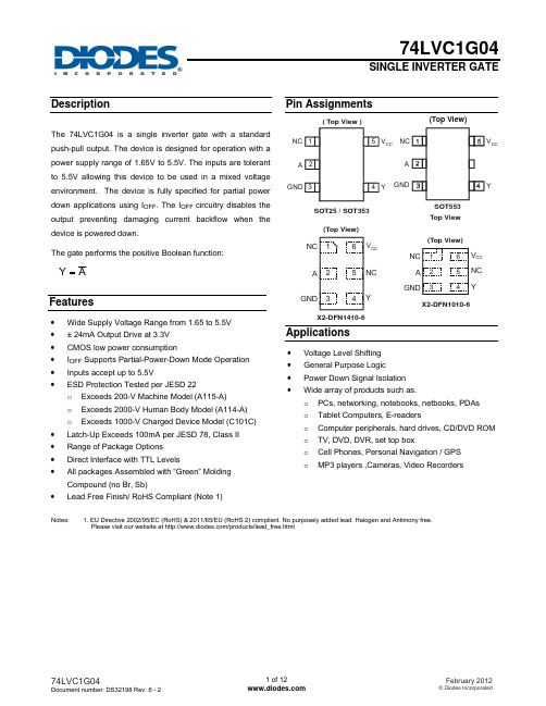
• Voltage Level Shifting • General Purpose Logic • Power Down Signal Isolation • Wide array of products such as.
VCC = 1.65V VCC = 2.3V
VCC = 3V
VCC = 4.5V
VCC = 1.65V
VCC = 2.3V
IOL
Low-level output current
74LVC1G14 单片1输入施密特触发器翻转器说明书
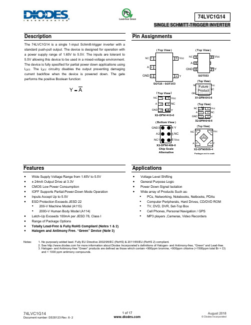
74LVC1G14SINGLE SCHMITT-TRIGGER INVERTERNotes: 1. No purposely added lead. Fully EU Directive 2002/95/EC (RoHS) & 2011/65/EU (RoHS 2) compliant.2. See for more information about Diodes Incorporated’s definitions of Halogen- and Antimony-free, "Green" and Lead-free.3. Halogen- and Antimony-free "Green” products are defined as those which contain <900ppm bromine, <900ppm chlorine (<1500ppm total Br + Cl) and < 1000 ppm antimony compounds.DescriptionThe 74LVC1G14 is a single 1-input Schmitt-trigger inverter with a standard push-pull output. The device is designed for operation with a power supply range of 1.65V to 5.5V. The inputs are tolerant to 5.5V allowing this device to be used in a mixed-voltage environment. The device is fully specified for partial power down applications using I OFF . The I OFF circuitry disables the output preventing damaging current backflow when the device is powered down. The gate performs the positive Boolean function:AY =Pin AssignmentsX2-DFN1410-6AX2-DFN1010-6YVccSOT25 / SOT353(Top View )YVccSOT553(Top View )X2-DFN0808-4Packages not to scaleX2-DFN1409-6Chip Scale AlternativeGNDA Y NC NC Vcc(Bottom View )X1-DFN1010-6NCGND VccYNC A 123456Features• Wide Supply Voltage Range from 1.65V to 5.5V • ± 24mA Output Drive at 3.3V • CMOS Low Power Consumption• IOFF Supports Partial-Power-Down Mode Operation • Inputs Accept Up to 5.5V•ESD Protection Exceeds JESD 22 ▪ 200-V Machine Model (A115)▪ 2000-V Human Body Model (A114)• Latch-Up Exceeds 100mA per JESD 78, Class I • Range of Package Options• Totally Lead-Free & Fully RoHS Compliant (Notes 1 & 2) •Halogen and Antimony Free. “Green” Device (Note 3)Applications• Voltage Level Shifting • General Purpose Logic• Power Down Signal Isolation • Wide array of Products Such as : ▪ PCs, Networking, Notebooks, Netbooks, PDAs ▪ Computer Peripherals, Hard Drives, CD/DVD ROM ▪ TV, DVD, DVR, Set-Top Box▪ Cell Phones, Personal Navigation / GPS ▪MP3 players ,Cameras, Video RecordersFuture ProductOrdering InformationLVC : 1.65 to 5.5 V Schmitt Trigger SE : SOT353Logic Family Inverter Z : SOT5531G : One Gate FS3 : X2-DFN0808-4 FW5 : X1-DFN1010-6 FW4 :X2-DFN1010-6 FX4 : X2- DFN1409-6FZ4 : X2- DFN1410-6Notes: 4. Pad layout as shown on Diodes’ suggested pad layout, which can be found on our website at /package-outlines.html.5. The taping orientation is located on our website at https:///assets/Diodes-Packaging/ap02007.pdf.Pin DescriptionsPin NameDescriptionA Data Input GND Ground Y Data Output V CCSupply VoltageLogic DiagramAYDevicePackage Code Package (Notes 4 & 5) Package Size7” Tape and Reel QuantityPart Number Suffix74LVC1G14W5-7 W5 SOT25 3.0mm × 2.8mm × 1.2mm 0.95mm Lead Pitch 3000/Tape & Reel -7 74LVC1G14SE-7 SE SOT353 2.0mm × 2.0mm × 1.1mm 0.65mm Lead Pitch 3000/Tape & Reel -7 74LVC1G14Z-7 SE SOT553 1.6mm × 1.6 mm × 0.62mm0.5mm Lead Pitch 4000/Tape & Reel -7 74LVC1G14FS3-7 FS3 X2-DFN0808-4 0.9mm × 0.9 mm × 0.35mm 0.5mm Pad Pitch (Diamond) 5000/Tape & Reel -7 74LVC1G14FW5-7 (Future Product) FW5 X1-DFN1010-6 (Future Product) 1.0mm × 1.0mm × 0.5mm0.35mm Pad Pitch 5000/Tape & Reel -7 74LVC1G14FW4-7 FW4 X2-DFN1010-6 1.0mm × 1.0mm × 0.4mm0.35mm Pad Pitch 5000/Tape & Reel -7 74LVC1G14FX4-7 FX4 X2-DFN1409-6 (Chip Scale Alternative)1.4mm × 0.9mm × 0.4mm0.5mm Pad Pitch 5000/Tape & Reel -7 74LVC1G14FZ4-7FZ4X2-DFN1410-61.4mm × 1.0mm × 0.4mm0.5mm Pad Pitch5000/Tape & Reel-7Notes: 6. Stresses beyond the Absolute Maximum Ratings may result in immediate failure or reduced reliability. These are stress values and device operation should be within recommend values.7. Forcing the maximum allowed voltage could cause a condition exceeding the maximum current or conversely forcing the maximum current couldcause a condition exceeding the maximum voltage. The ratings of both current and voltage must be maintained within the controlled range.. Recommended Operating Conditions(Note 8)Symbol Parameter Min Max UnitV CC Operating Voltage Operating 1.65 5.5 V Data Retention Only 1.5 — VV I Input Voltage 0 5.5 V V O Output Voltage 0 V CC VI OH High-Level Output Current V CC = 1.65V — -4mA V CC = 2.3V — -8V CC = 2.7V — -12V CC = 3V— -16— -24V CC = 4.5V — -32I OL Low-Level Output Current V CC = 1.65V — 4mA V CC = 2.3V — 8V CC = 2.7V — 12V CC = 3V— 16— 24V CC = 4.5V — 32T A Operating Free-Air Temperature — -40 +125 °C Note: 8. Unused inputs should be held at V CC or Ground.74LVC1G14Electrical Characteristics (continued) (@T A = -40°C to +125°C. All typical values are at V CC = 3.3V, T A = +25°C)Symbol Parameter Test Conditions V CC Min Typ. Max UnitV T+Positive- Going InputThreshold Voltage— 1.65V 0.70 — 1.20 —— 2.3V 1.11 — 1.60 —— 3V 1.50 — 2.00 —— 4.5V 2.16 — 2.74 —— 5.5V 2.61 — 3.33 —V T-Negative- Going InputThreshold Voltage— 1.65V 0.30 — 0.75 —— 2.3V 0.58 — 1.03 —— 3V 0.80 — 1.33 —— 4.5V 1.21 — 1.95 —— 5.5V 1.45 — 2.35 —ΔV T Hysteresis(V T+- V T-)— 1.65V 0.30 — 0.62 —— 2.3V 0.37 — 0.80 —— 3V 0.32 — 1.00 —— 4.5V 0.50 — 1.20 —— 5.5V 0.55 — 1.40 —V OH High Level Output Voltage I OH = -100μA 1.65V to 5.5V V CC– 0.1 — —V I OH = -4mA 1.65V 0.95 — —I OH = -8mA 2.3V 1.7 — —I OH = -12mA 2.7V 1.9 — —I OH = -16mA3V1.9 — —I OH = -24mA 2.0 — —I OH = -32mA 4.5V 3.4 — —V OL Low-Level Output Voltage I OL= 100μA 1.65V to 5.5V — — 0.1V I OL = 4mA 1.65V — — 0.7I OL = 8mA 2.3V — — 0.45I OL = 12mA 2.7V — — 0.6I OL = 16mA3V— — 0.6I OL = 24mA — — 0.8I OL = 32mA 4.5V — — 0.8I I Input Current V I = 5.5V or GND 0 to 5.5V — — ± 100 µA I OFF Power Down Leakage Current V I or V O= 5.5V 0 — — ± 200 µAI CC Supply Current V I = 5.5V of GNDI O = 01.65V to 5.5V — — 200 µAΔI CC Additional Supply Current Input at V CC –0.6V 3V to 5.5V — — 5000 µANote: 9. Test condition for each of the 8 package types: Device mounted on FR-4 substrate PC board, 2oz copper, with minimum recommended pad layout.Switching CharacteristicsT A= -40°C to +85°C, C L = 15pF as noted (see Figure 1)Parameter FromInputToOutputV CC = 1.8V± 0.15VV CC = 2.5V± 0.2VV CC = 3.3V± 0.3VV CC = 5V± 0.5V UnitMin Max Min Max Min Max Min Maxt pd A Y 1.0 9.9 0.7 5.5 0.7 4.6 0.7 4.4 ns T A = -40°C to +85°C, C L = 30 or 50pF as noted (See Figure 2)Parameter FromInputToOutputV CC = 1.8V± 0.15VV CC = 2.5V± 0.2VV CC = 3.3V± 0.3VV CC = 5V± 0.5V UnitMin Max Min Max Min Max Min Maxt pd A Y 1.0 11 0.7 6.5 0.7 5.5 0.7 5 ns T A= -40°C to +125°C, C L = 15pF as noted (See Figure 1)Parameter FromInputToOutputV CC = 1.8V± 0.15VV CC = 2.5V± 0.2VV CC = 3.3V± 0.3VV CC = 5V± 0.5V UnitMin Max Min Max Min Max Min Maxt pd A Y 1.0 12.5 0.7 7.5 0.7 6.5 0.7 5.5 ns T A = -40°C to +125°C, C L = 30 or 50pF as noted (See Figure 2)Parameter FromInputToOutputV CC = 1.8V± 0.15VV CC = 2.5V± 0.2VV CC = 3.3V± 0.3VV CC = 5V± 0.5V UnitMin Max Min Max Min Max Min Maxt pd A Y 1.0 14.0 0.7 8.5 0.7 7.0 0.7 6.5 nsOperating CharacteristicsT A = +25°CParameterTest Conditions V CC = 1.8V V CC = 2.5V V CC = 3.3V V CC = 5V Unit Typ. Typ. Typ. Typ. C pdPower Dissipation Capacitancef = 10 MHz20212225pFParameter Measurement InformationR LC L(see Note A)From Output Under TestV CCInputsV MC L R LV It r /t f 1.8V±0.15V V CC ≤2ns V CC /2 15pF 1M Ω2.5V±0.2V V CC ≤2ns V CC /2 15pF 1M Ω3.3V±0.3V 3V ≤2.5ns 1.5V 15pF 1M Ω 5V±0.5VV CC≤2.5nsV CC /215pF1M ΩV l0 VVoltage Waveform Pulse DurationV l0 V V OHV OLV OHV OLVoltage Waveform Propagation Delay TimesInverting and Non Inverting OutputsFigure 1. Load Circuit and Voltage WaveformsNotes: A. Includes test lead and test apparatus capacitance.B. All pulses are supplied at pulse repetition rate ≤ 10MHz .C. Inputs are measured separately one transition per measurement.D. t PLH and t PHL are the same as t PD .Parameter Measurement Information (continued)R LC L(see Note A)From Output Under TestV CC InputsV M C L R LV I t r /t f 1.8V±0.15V V CC ≤2ns V CC /2 30pF 1k Ω2.5V±0.2V V CC ≤2ns V CC /2 30pF 500Ω3.3V±0.3V 3V ≤2.5ns 1.5V 50pF 500Ω 5V±0.5VV CC≤2.5nsV CC /250pF500ΩV l0 VVoltage Waveform Pulse DurationV l0 V V OHV OLV OHV OLVoltage Waveform Propagation Delay TimesInverting and Non Inverting OutputsFigure 2. Load Circuit and Voltage WaveformsNotes: A. Includes test lead and test apparatus capacitance.B. All pulses are supplied at pulse repetition rate ≤ 10MHz .C. Inputs are measured separately one transition per measurement.D. t PLH and t PHL are the same as t PD .Marking Information(1) SOT25, SOT353, and SOT553XX Y W X : Identification Code : Year 0~9: Week : A~Z : 1~26 week; a~z : 27~52 week;z represents 52 and 53 week : A~Z : Internal Code(Top Views)SOT25/353SOT553Part Number Package Identification Code74LVC1G14W5-7 SOT25 UP 74LVC1G14SE-7 SOT353 UP 74LVC1G14Z-7SOT553UP(2) DFN PackagesPart Number Package Identification Code74LVC1G14FS3-7 X2-DFN0808-4WP 74LVC1G14FW5-7 X1-DFN1010-6 V8 74LVC1G14FW4-7 X2-DFN1010-6 UP 74LVC1G14FX4-7 X2-DFN1409-6 MG 74LVC1G14FZ4-7X2-DFN1410-6UPPackage Outline DimensionsPlease see /package-outlines.html for the latest version.(1) Package Type: SOT25SOT25Dim Min Max Typ A 0.35 0.50 0.38 B 1.50 1.70 1.60 C 2.70 3.00 2.80 D — — 0.95 H 2.90 3.10 3.00 J 0.013 0.10 0.05 K 1.00 1.30 1.10 L 0.35 0.55 0.40 M 0.10 0.20 0.15 N 0.70 0.80 0.75 a 0° 8° — All Dimensions in mm(2) Package Type: SOT353SOT353SOT353Dim Min Max Typ A1 0.00 0.10 0.05 A2 0.90 1.00 0.95 b 0.10 0.30 0.25 c 0.10 0.22 0.11 D 1.80 2.20 2.15 E 2.00 2.20 2.10 E1 1.15 1.35 1.30 e 0.650 BSC F 0.40 0.45 0.425 L 0.25 0.40 0.30 a 0° 8° — All Dimensions in mmPlease see /package-outlines.html for the latest version.(3) Package Type: SOT553(4) Package Type X2-DFN0808-4Please see /package-outlines.html for the latest version.(5) Package Type: X1-DFN1010-6(Future Product)(6) Package Type X2-DFN1010-6X2-DFN1010-6X2-DFN1010-6 Dim Min Max Typ A — 0.40 0.39 A1 0.00 0.05 0.02 A3 ——0.13 b 0.14 0.20 0.17 b1 0.05 0.15 0.10 D 0.95 1.05 1.00 E 0.95 1.05 1.00 e — — 0.35 L 0.35 0.450.40 K 0.15 — — Z——0.065All Dimensions in mm(7) Package Type: X2-DFN1409-66x)74LVC1G14Package Outline Dimensions (continued)Please see /package-outlines.html for the latest version.(8) Package Type: X2-DFN1410-6b(6x)Z1(4x)Suggested Pad LayoutPlease see /package-outlines.html for the latest version.(1) Package Type: SOT25(2) Package Type: SOT353DimensionsValue (in mm) C 0.650 C1 1.900 G 1.300 X 0.420 X1 1.720 Y 0.600 Y12.500(3) Package Type: SOT553XZYC1C2C2G XZYC1C2C2GPlease see /package-outlines.html for the latest version.(4) Package Type X2-DFN0808-4Dimensions ValueC 0.480X 0.320X1 0.300X2 0.106X3 0.800Y 0.320Y1 0.300Y20.106Y3 0.900(5) Package Type X1-DFN1010-6(Future Product)(6) Package Type X2-DFN1010-6DimensionsValue (in mm)C 0.350 G 0.150 X 0.200 X1 0.900 Y 0.550 Y1 1.250Please see /package-outlines.html for the latest version.(7) Package Type: X2-DFN1409-6DimensionsValue (in mm)C 1.000C1 0.500D 0.300G 0.200G1 0.200X 0.400Y 0.150 (8) Package Type: X2-DFN1410-6DimensionsValue (in mm)C 0.500G 0.250X 0.250X1 1.250Y 0.525Y1 1.250 6x)74LVC1G14。
74LVT14资料

元器件交易网SO14:plastic small outline package; 14 leads; body width 3.9 mm SOT108-1SSOP14:plastic shrink small outline package; 14 leads; body width 5.3 mm SOT337-1TSSOP14:plastic thin shrink small outline package; 14 leads; body width 4.4 mm SOT402-1NOTESPhilips Semiconductors and Philips Electronics North America Corporation reserve the right to make changes, without notice, in the products,including circuits, standard cells, and/or software, described or contained herein in order to improve design and/or performance. Philips Semiconductors assumes no responsibility or liability for the use of any of these products, conveys no license or title under any patent, copyright,or mask work right to these products, and makes no representations or warranties that these products are free from patent, copyright, or mask work right infringement, unless otherwise specified. Applications that are described herein for any of these products are for illustrative purposes only. Philips Semiconductors makes no representation or warranty that such applications will be suitable for the specified use without further testing or modification.LIFE SUPPORT APPLICATIONS Philips Semiconductors and Philips Electronics North America Corporation Products are not designed for use in life support appliances, devices,or systems where malfunction of a Philips Semiconductors and Philips Electronics North America Corporation Product can reasonably be expected to result in a personal injury. Philips Semiconductors and Philips Electronics North America Corporation customers using or selling Philips Semiconductors and Philips Electronics North America Corporation Products for use in such applications do so at their own risk and agree to fully indemnify Philips Semiconductors and Philips Electronics North America Corporation for any damages resulting from such improper use or sale.This data sheet contains preliminary data, and supplementary data will be published at a later date. PhilipsSemiconductors reserves the right to make changes at any time without notice in order to improve designand supply the best possible product.Philips Semiconductors 811 East Arques Avenue P .O. Box 3409Sunnyvale, California 94088–3409Telephone 800-234-7381DEFINITIONSData Sheet Identification Product Status DefinitionObjective Specification Preliminary Specification Product Specification Formative or in Design Preproduction Product Full Production This data sheet contains the design target or goal specifications for product development. Specificationsmay change in any manner without notice.This data sheet contains Final Specifications. Philips Semiconductors reserves the right to make changesat any time without notice, in order to improve design and supply the best possible product.Philips Semiconductors and Philips Electronics North America Corporation register eligible circuits under the Semiconductor Chip Protection Act.© Copyright Philips Electronics North America Corporation 1996All rights reserved. Printed in U.S.A.。
SN74LVC1G14_08中文资料
FUNCTION TABLE
INPUT A
H
L
OUTPUT Y
L
H
LOGIC DIAGRAM (POSITIVE LOGIC) (DBV, DCK, DRL, DRY, and YZP Package)
A2
4Y
LOGIC DIAGRAM (POSITIVE LOGIC) (YZV Package)
A1
____ CF
CF_ C14_
CF_ CF_
(1) Package drawings, standard packing quantities, thermal data, symbolization, and PCB design guidelines are available at /sc/package.
NanoFree is a trademark of Texas Instruments.
PRODUCTION DATA information is current as of publication date. Products conform to specifications per the terms of the Texas Instruments standard warranty. Production processing does not necessarily include testing of all parameters.
– 1000-V Charged-Device Model (C101)
DCK PACKAGE (TOP VIEW)
DRL PACKAGE (TOP VIEW)
NC
1
5
VCC
NC
1
74LVC1G14单芯片阈值稳定器反转器数据表说明书

74LVC1G14Single Schmitt-trigger inverterRev. 15 — 8 June 2018Product data sheet1General descriptionThe 74LVC1G14 provides the inverting buffer function with Schmitt-trigger input. It iscapable of transforming slowly changing input signals into sharply defined, jitter-freeoutput signals.The input can be driven from either 3.3 V or 5 V devices. This feature allows the useof this device in a mixed 3.3 V and 5 V environment. Schmitt-trigger action at the inputmakes the circuit tolerant for slower input rise and fall time.This device is fully specified for partial power-down applications using I OFF. The I OFFcircuitry disables the output, preventing the damaging backflow current through thedevice when it is powered down.2Features and benefits•Wide supply voltage range from 1.65 V to 5.5 V•High noise immunity•Complies with JEDEC standard:–JESD8-7 (1.65 V to 1.95 V)–JESD8-5 (2.3 V to 2.7 V)–JESD8-B/JESD36 (2.7 V to 3.6 V).•±24 mA output drive (V CC = 3.0 V)•CMOS low power consumption•Latch-up performance exceeds 250 mA•Direct interface with TTL levels•Unlimited rise and fall times•Input accepts voltages up to 5 V•Multiple package options•ESD protection:–HBM: ANSI/ESDA/JEDEC JS-001 Class 2 exceeds 2000 V–MM: JESD22-A115-A exceeds 200 V.•Specified from -40 °C to +85 °C and -40 °C to +125 °C.3Applications•Wave and pulse shaper•Astable multivibrator•Monostable multivibratorSingle Schmitt-trigger inverter 4Ordering information5Marking[1]The pin 1 indicator is located on the lower left corner of the device, below the marking code.Single Schmitt-trigger inverter6Functional diagram7Pinning information7.1Pinning74LVC1G14n.c.V CCA GNDY001aab65512354Figure 4. Pin configuration SOT353-1 and SOT75374LVC1G14A 001aae976n.c.GNDn.c.V CC YT ransparent top view231546Figure 5. Pin configuration SOT886, SOT891, SOT1115and SOT1202n.c.V CCGND13254AY aaa-003024Transparent top view 74LVC1G14Figure 6. Pin configuration SOT1226 (X2SON5)aaa-028401Transparent top view74LVC1G14V CC4Y3A 1GND 2Figure 7. Pin configuration SOT1269-2 (X2SON4)7.2Pin descriptionSingle Schmitt-trigger inverter8Functional description[1][1]H = HIGH voltage level; L = LOW voltage level9Limiting valuesTable 5. Limiting valuesIn accordance with the Absolute Maximum Rating System (IEC 60134). Voltages are referenced to GND (ground = 0 V).[1]The input and output voltage ratings may be exceeded if the input and output current ratings are observed.[2]For TSSOP5 and SC-74A packages: above 87.5 °C the value of P tot derates linearly with 4.0 mW/K.For XSON6 and X2SON5 package: above 118 °C the value of P tot derates linearly with 7.8 mW/K.[3]For X2SON4 packages: above 57 °C the value of P tot derates linearly with 1.7 mW/K.Single Schmitt-trigger inverter 10Recommended operating conditions11Static characteristicsTable 7. Static characteristicsAt recommended operating conditions; voltages are referenced to GND (ground = 0 V).Single Schmitt-trigger inverter[1]All typical values are measured at maximum V CC and T amb = 25 °C.Table 8. Transfer characteristicsVoltages are referenced to GND (ground = 0 V); for test circuit see Figure 9.[1]Typical values are measured at T amb = 25 °C and V CC = 1.8 V, 2.5 V, 2.7 V, 3.3 V and 5.0 V respectively.Single Schmitt-trigger inverter 12Dynamic characteristicsTable 9. Dynamic characteristicsVoltages are referenced to GND (ground = 0 V); for test circuit see Figure 9.[1]Typical values are measured at T amb = 25 °C and V CC = 1.8 V, 2.5 V, 2.7 V, 3.3 V and 5.0 V respectively.[2]t pd is the same as t PLH and t PHL.[3]C PD is used to determine the dynamic power dissipation (P D in μW).P D = C PD x V CC2 x f i + (C L x V CC2 x f o) where:f i = input frequency in MHz;f o = output frequency in MHz;C L = output load capacitance in pF;V CC = supply voltage in V.12.1Waveform and test circuitSingle Schmitt-trigger inverterSingle Schmitt-trigger inverter12.2Waveforms transfer characteristics13Application informationThe slow input rise and fall times cause additional power dissipation, this can becalculated using the following formula:P add = f i x (t r x ΔI CC(AV) + t f x ΔI CC(AV)) x V CC where:•P add = additional power dissipation (μW);•f i = input frequency (MHz);•t r = input rise time (ns); 10 % to 90 %;•t f = input fall time (ns); 90 % to 10 %;•ΔI CC(AV) = average additional supply current (μA).Average ΔI CC(AV) differs with positive or negative input transitions, as shown in Figure 13.An example of a relaxation circuit using the 74LVC1G14 is shown in Figure 14.Single Schmitt-trigger inverteraaa-0219851234560.20.40.60.811.2V CC (V)KFigure 15. Typical K-factor for relaxation oscillatorSingle Schmitt-trigger inverter 14Package outlineSingle Schmitt-trigger inverterSingle Schmitt-trigger inverterSingle Schmitt-trigger inverterSingle Schmitt-trigger inverterSingle Schmitt-trigger inverterSingle Schmitt-trigger inverterSingle Schmitt-trigger inverterSingle Schmitt-trigger inverter 15Abbreviations16Revision historySingle Schmitt-trigger inverter 17Legal information17.1 Data sheet status[1]Please consult the most recently issued document before initiating or completing a design.[2]The term 'short data sheet' is explained in section "Definitions".[3]The product status of device(s) described in this document may have changed since this document was published and may differ in case of multipledevices. The latest product status information is available on the Internet at URL .17.2 DefinitionsDraft — The document is a draft version only. The content is still under internal review and subject to formal approval, which may result in modifications or additions. Nexperia does not give any representations or warranties as to the accuracy or completeness of information included herein and shall have no liability for the consequences of use of such information.Short data sheet — A short data sheet is an extract from a full data sheet with the same product type number(s) and title. A short data sheet is intended for quick reference only and should not be relied upon to contain detailed and full information. For detailed and full information see the relevant full data sheet, which is available on request via the local Nexperia sales office. In case of any inconsistency or conflict with the short data sheet, the full data sheet shall prevail.Product specification — The information and data provided in a Product data sheet shall define the specification of the product as agreed between Nexperia and its customer, unless Nexperia and customer have explicitly agreed otherwise in writing. In no event however, shall an agreement be valid in which the Nexperia product is deemed to offer functions and qualities beyond those described in the Product data sheet.17.3 DisclaimersLimited warranty and liability — Information in this document is believed to be accurate and reliable. However, Nexperia does not give any representations or warranties, expressed or implied, as to the accuracyor completeness of such information and shall have no liability for the consequences of use of such information. Nexperia takes no responsibility for the content in this document if provided by an information source outside of Nexperia. In no event shall Nexperia be liable for any indirect, incidental, punitive, special or consequential damages (including - without limitation -lost profits, lost savings, business interruption, costs related to the removal or replacement of any products or rework charges) whether or not such damages are based on tort (including negligence), warranty, breach of contract or any other legal theory. Notwithstanding any damages that customer might incur for any reason whatsoever, Nexperia's aggregate and cumulative liability towards customer for the products described herein shall be limited in accordance with the Terms and conditions of commercial sale of Nexperia.Right to make changes — Nexperia reserves the right to make changesto information published in this document, including without limitation specifications and product descriptions, at any time and without notice. This document supersedes and replaces all information supplied prior to the publication hereof.Suitability for use — Nexperia products are not designed, authorized or warranted to be suitable for use in life support, life-critical or safety-critical systems or equipment, nor in applications where failure or malfunctionof an Nexperia product can reasonably be expected to result in personal injury, death or severe property or environmental damage. Nexperia and its suppliers accept no liability for inclusion and/or use of Nexperia products in such equipment or applications and therefore such inclusion and/or use is at the customer’s own risk.Applications — Applications that are described herein for any of these products are for illustrative purposes only. Nexperia makes no representation or warranty that such applications will be suitable for the specified use without further testing or modification. Customers are responsible for the design and operation of their applications and products using Nexperia products, and Nexperia accepts no liability for any assistance with applications or customer product design. It is customer’s sole responsibility to determine whether the Nexperia product is suitable and fit for the customer’s applications and products planned, as well as for the planned application and use of customer’s third party customer(s). Customers should provide appropriate design and operating safeguards to minimize the risks associated with their applications and products. Nexperia does not accept any liability related to any default, damage, costs or problem which is based on any weakness or default in the customer’s applications or products, or the application or use by customer’s third party customer(s). Customer is responsible for doing all necessary testing for the customer’s applications and products using Nexperia products in order to avoid a default of the applications and the products or of the application or use by customer’s third party customer(s). Nexperia does not accept any liability in this respect.Limiting values — Stress above one or more limiting values (as defined in the Absolute Maximum Ratings System of IEC 60134) will cause permanent damage to the device. Limiting values are stress ratings only and (proper) operation of the device at these or any other conditions above thosegiven in the Recommended operating conditions section (if present) or the Characteristics sections of this document is not warranted. Constant or repeated exposure to limiting values will permanently and irreversibly affect the quality and reliability of the device.Terms and conditions of commercial sale — Nexperia products aresold subject to the general terms and conditions of commercial sale, as published at /profile/terms, unless otherwise agreed in a valid written individual agreement. In case an individual agreement is concluded only the terms and conditions of the respective agreement shall apply. Nexperia hereby expressly objects to applying the customer’s general terms and conditions with regard to the purchase of Nexperia products by customer.No offer to sell or license — Nothing in this document may be interpreted or construed as an offer to sell products that is open for acceptance orthe grant, conveyance or implication of any license under any copyrights, patents or other industrial or intellectual property rights.Export control — This document as well as the item(s) described herein may be subject to export control regulations. Export might require a prior authorization from competent authorities.Single Schmitt-trigger inverterNon-automotive qualified products — Unless this data sheet expressly states that this specific Nexperia product is automotive qualified, the product is not suitable for automotive use. It is neither qualified nor tested in accordance with automotive testing or application requirements. Nexperia accepts no liability for inclusion and/or use of non-automotive qualified products in automotive equipment or applications. In the event that customer uses the product for design-in and use in automotive applications to automotive specifications and standards, customer (a) shall use the product without Nexperia's warranty of the product for such automotive applications, use and specifications, and (b) whenever customer uses the product for automotive applications beyond Nexperia's specifications such use shall be solely at customer’s own risk, and (c) customer fully indemnifies Nexperia for any liability, damages or failed product claims resulting from customer design and use of the product for automotive applications beyond Nexperia's standard warranty and Nexperia's product specifications.Translations — A non-English (translated) version of a document is for reference only. The English version shall prevail in case of any discrepancy between the translated and English versions.17.4 TrademarksNotice: All referenced brands, product names, service names and trademarks are the property of their respective owners.74LVC1G14All information provided in this document is subject to legal disclaimers.© Nexperia B.V. 2018. All rights reserved. Product data sheet Rev. 15 — 8 June 201821 / 22Single Schmitt-trigger inverterContents1General description (1)2Features and benefits (1)3Applications (1)4Ordering information (2)5Marking (2)6Functional diagram (3)7Pinning information (3)7.1Pinning (3)7.2Pin description (3)8Functional description (4)9Limiting values (4)10Recommended operating conditions (5)11Static characteristics (5)12Dynamic characteristics (7)12.1Waveform and test circuit (7)12.2Waveforms transfer characteristics (9)13Application information (9)14Package outline (11)15Abbreviations (19)16Revision history (19)17Legal information (20)Please be aware that important notices concerning this document and the product(s)described herein, have been included in section 'Legal information'.© Nexperia B.V. 2018.All rights reserved.For more information, please visit: Forsalesofficeaddresses,pleasesendanemailto:***************************Date of release: 8 June 2018Document identifier: 74LVC1G14Mouser ElectronicsAuthorized DistributorClick to View Pricing, Inventory, Delivery & Lifecycle Information:N experia:74LVC1G14GS,13274LVC1G14GN,13274LVC1G14GF,13274LVC1G14GM,11574LVC1G14GM,132 74LVC1G14GV,12574LVC1G14GW,12574LVC1G14GX,12574LVC1G14GX4Z。
74HCT14中文资料
Fig.4 IEC logic symbol.
2003 Oct 30
4
元器件交易网
Philips Semiconductors
Product specification
Hex inverting Schmitt trigger
74HC14; 74HCT14
handbook, halfpage
2003 Oct 30
2
元器件交易网
Philips Semiconductors
Product specification
Hex inverting Schmitt trigger
FUNCTION TABLE INPUT nA L H Note 1. H = HIGH voltage level; L = LOW voltage level. ORDERING INFORMATION PACKAGE TYPE NUMBER TEMPERATURE RANGE 74HC14D 74HCT14D 74HC14DB 74HCT14DB 74HC14N 74HCT14N 74HC14PW 74HCT14PW 74HC14BQ 74HCT14BQ PINNING PIN 1 2 3 4 5 6 7 8 9 10 11 12 13 14 1A 1Y 2A 2Y 3A 3Y GND 4Y 4A 5Y 5A 6Y 6A VCC SYMBOL data input data output data input data output data input data output ground (0 V) data output data input data output data input data output data input supply voltage −40 to +125 °C −40 to +125 °C −40 to +125 °C −40 to +125 °C −40 to +125 °C −40 to +125 °C −40 to +125 °C −40 to +125 °C −40 to +125 °C −40 to +125 °C PINS 14 14 14 14 14 14 14 14 14 14 PACKAGE SO14 SO14 SSOP14 SSOP14 DIP14 DIP14 TSSOP14 TSSOP14 DHVQFN14 DHVQFN14
M74HCT14M1R中文资料
DIM.
P001A
5/9
元器件交易网
M54/M74HCT14
Ceramic DIP14/1 MECHANICAL DATA
mm MIN. A B D E e3 F G H L M N P Q 7.8 2.29 0.4 1.17 0.22 1.52 0.38 15.24 2.79 0.55 1.52 0.31 2.54 10.3 8.05 5.08 0.307 0.090 0.016 0.046 0.009 0.060 3.3 0.015 0.600 0.110 0.022 0.060 0.012 0.100 0.406 0.317 0.200 TYP. MAX. 20 7.0 0.130 MIN. inch TYP. MAX. 0.787 0.276
Input Leakage Current Quiescent Supply Current
5.5 5.5
3/9
元器件交易网
M54/M74HCT14
AC ELECTRICAL CHARACTERISTICS (C L = 50 pF, Input t r = tf = 6 ns)
B1R (Plastic Package)
F1R (Ceramic Package)
M1R (Micro Package)
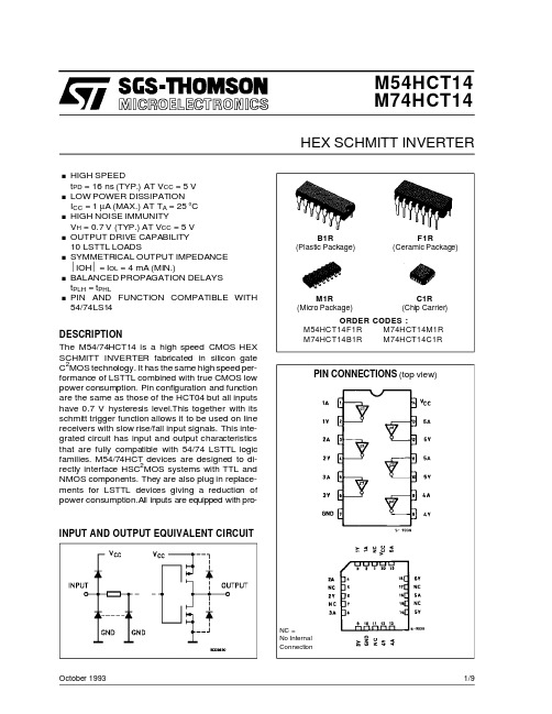
C1R (Chip Carrier)
DESCRIPTION The M54/74HCT14 is a high speed CMOS HEX SCHMITT INVERTER fabricated in silicon gate C2MOS technology. It has the same high speed performance of LSTTL combined with true CMOS low power consumption. Pin configuration and function are the same as those of the HCT04 but all inputs have 0.7 V hysteresis level.This together with its schmitt trigger function allows it to be used on line receivers with slow rise/fall input signals. This integrated circuit has input and output characteristics that are fully compatible with 54/74 LSTTL logic families. M54/74HCT devices are designed to directly interface HSC2MOS systems with TTL and NMOS components. They are also plug in replacements for LSTTL devices giving a reduction of power consumption.All inputs are equipped with pro-
常用74系列标准数字电路的中文名称资料
常用74系列标准数字电路的中文名称资料收藏常用74系列标准数字电路的中文名称资料器件代号器件名称74 74LS 74HC00 四2输入端与非门√√√01 四2输入端与非门(OC) √√02 四2输入端或非门√√√03 四2输入端与非门(OC) √√04 六反相器√√√05 六反相器(OC) √√06 六高压输出反相器(OC,30V) √√07 六高压输出缓冲,驱动器(OC,30V) √√√08 四2输入端与门√√√09 四2输入端与门(OC) √√√10 三3输入端与非门√√√11 三3输入端与门√√12 三3输入端与非门(OC) √√√13 双4输入端与非门√√√14 六反相器√√√15 三3输入端与门(OC) √√16 六高压输出反相器(OC,15V) √17 六高压输出缓冲,驱动器(OC,15V) √20 双4输入端与非门√√√21 双4输入端与门√√√22 双4输入端与非门(OC) √√25 双4输入端或非门(有选通端) √√√26 四2输入端高压输出与非缓冲器√√√27 三3输入端或非门√√√28 四2输入端或非缓冲器√√√器件代号器件名称74 74LS 74HC30 8输入端与非门√√√32 四2输入端或门√√√33 四2输入端或非缓冲器(OC) √√37 四2输入端与非缓冲器√√38 四2输入端与非缓冲器(OC) √√40 双4输入端与非缓冲器√√√42 4线-10线译码器(BCD输入) √√43 4线-10线译码器(余3码输入) √44 4线-10线译码器(余3葛莱码输入) √48 4线-7段译码器√49 4线-7段译码器√50 双2路2-2输入与或非门√√√51 2路3-3输入,2路2-2输入与或非门√√√52 4路2-3-2-2输入与或门√53 4路2-2-2-2输入与或非门√54 4路2-3-3-2输入与或非门√√55 2路4-4输入与或非门√60 双4输入与扩展器√√61 三3输入与扩展器√62 4路2-3-3-2输入与或扩展器√64 4路4-2-3-2输入与或非门√65 4路4-2-3-2输入与或非门(OC) √70 与门输入J-K触发器√71 与或门输入J-K触发器√72 与门输入J-K触发器√器件代号器件名称74 74LS 74HC74 双上升沿D型触发器√√78 双D型触发器√√85 四位数值比较器√86 四2输入端异或门√√√87 4位二进制原码/反码√95 4位移位寄存器√101 与或门输入J-K触发器√102 与门输入J-K触发器√107 双主-从J-K触发器√108 双主-从J-K触发器√74F74是高速的TTL芯片和74HC一样就是速度高109 双主-从J-K触发器√110 与门输入J-K触发器√111 双主-从J-K触发器√√112 双下降沿J-K触发器√113 双下降沿J-K触发器√114 双下降沿J-K触发器√116 双4位锁存器√120 双脉冲同步驱动器√121 单稳态触发器√√√122 可重触发单稳态触发器√√√123 可重触发双稳态触发器√√√125 四总线缓冲器√√√126 四总线缓冲器√√√128 四2输入端或非线驱动器√√√132 四2输入端与非门√√√d触发器芯片有:74HC74 74LS90 双D触发器74LS7474LS364八D触发器(三态)7474、74 H74、74F74、74ALS74、74L74、74LS74A、74S74、74HC73、74C74双D型正沿触发器(带预置和清除端)74174、74LS174、74F174、74ALS174、74S174、74HC174、74C174六D型触发器(带清除端)74175、74LS175、74F175、74ALS175、74S175、74HC175、74C175 四D型触发器(带清除端)74273、74LS273、74S273、74F273、74ALS273、74HC273 八D型触发器(带清除端)74LS364八D触发器(三态)74LS377、74F377、74S3777八D 触发器74LS378、74F378、74S378、74HC378六D 触发器74LS379、74F379、74S379、74HC379八D 触发器。
SN74LVC1G04YZAR中文资料
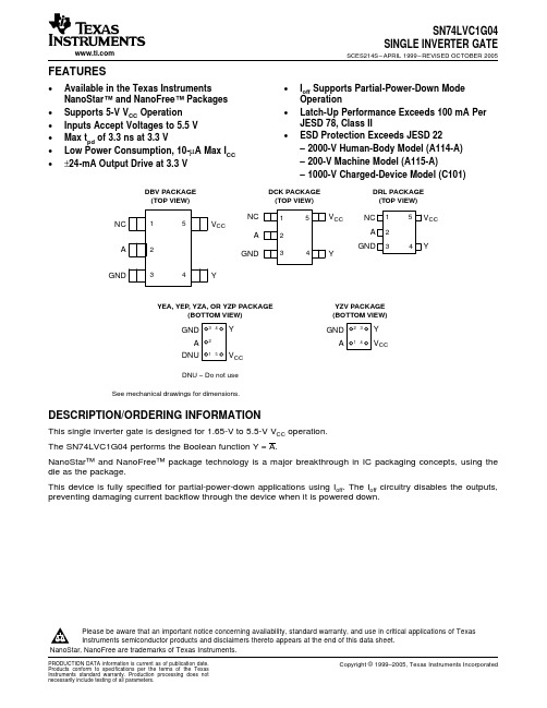
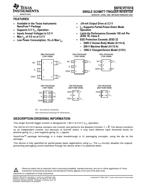
NanoFree™ – WCSP (DSBGA) 0.23-mm Large Bump – YZP (Pb-free)
NanoStar™ – WCSP (DSBGA) 0.23-mm Large Bump – YZV (Pb-free)
DCK PACKAGE (TOP VIEW)
DRL PACKAGE (TOP VIEW)
NC
1
A
2
5
VCC
NC
1
5
VCC
NC 1
5 VCC
A
2
A2
GND
3
4Y
GND 3 4 Y
GND
3
4
Y
YEA, YEP, YZA, OR YZP PACKAGE (BOTTOM VIEW)
GND 3 4 Y A2
DNU 1 5 VCC
SN74LVC1G04 SINGLE INVERTER GATE
SCES214S – APRIL 1999 – REVISED OCTOBER 2005
• Ioff Supports Partial-Power-Down Mode Operation
• Latch-Up Performance Exceeds 100 mA Per JESD 78, Class II
VO
Voltage range applied to any output in the high or low state(2)(3)
IIK
Input clamp current
VI < 0
IOK
Output clamp current
HD74LV1GT14AVS资料
Note: Unused or floating inputs must be held high or low.
4
HD74LV1GT14A
Electrical Characteristic
• Ta = –40 to 85°C
Item Input voltage Symbol VCC (V) * VT
HD74LV1GT14A
Inverter with Schmitt-trigger Input
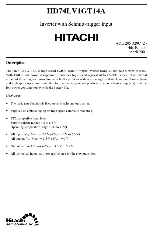
ADE-205-329C (Z) 4th. Edition April 2001 Description
The HD74LV1GT14A is high speed CMOS schmitt-trigger inverter using silicon gate CMOS process. With CMOS low power dissipation, it provides high speed equivalent to LS–TTL series. The internal circuit of three stages construction with buffer provides wide noise margin and stable output. Low voltage and high speed operation is suitable for the battery powered products (e.g., notebook computers), and the low power consumption extends the battery life.
Unit Test
FROM
TO (Output) Y
电子行业74系列芯片中文资料超级全

电子行业74系列芯片中文资料超级全CD4506双二组2输入可扩展或非门CD4508双4位锁存D型触发器CD4510可预置BCD码加/减计数器CD4511BCD锁存,7段译码,驱动器CD4512八路数据选择器CD4513BCD锁存,7段译码,驱动器(消隐)CD45144位锁存,4线-16线译码器CD45154位锁存,4线-16线译码器CD4516可预置4位二进制加/减计数器CD4517双64位静态移位寄存器CD4518双BCD同步加计数器CD4519四位与或选择器CD4520双4位二进制同步加计数器CD452124级分频器CD4522可预置BCD同步1/N计数器CD4526可预置4位二进制同步1/N计数器CD4527BCD比例乘法器CD4528双单稳态触发器CD4529双四路/单八路模拟开关CD4530双5输入端优势逻辑门CD453112位奇偶校验器CD45328位优先编码器CD4536可编程定时器CD4538精密双单稳CD4539双四路数据选择器CD4541可编程序振荡/计时器CD4543BCD七段锁存译码,驱动器CD4544BCD七段锁存译码,驱动器CD4547BCD七段译码/大电流驱动器CD4549函数近似寄存器CD4551四2通道模拟开关CD4553三位BCD计数器CD4555双二进制四选一译码器/分离器CD4556双二进制四选一译码器/分离器CD4558BCD八段译码器CD4560"N"BCD加法器CD4561"9"求补器CD4573四可编程运算放大器CD4574四可编程电压比较器CD4575双可编程运放/比较器CD4583双施密特触发器CD4584六施密特触发器CD45854位数值比较器CD45998位可寻址锁存器。
74LX1G14CTR, 规格书,Datasheet 资料
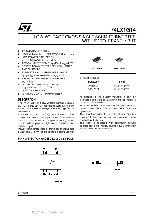
1/11April 2004s 5V TOLERANT INPUTSs HIGH SPEED:t PD =7.5ns (MAX.)at V CC =3V sLOW POWER DISSIPATION:I CC =1µA (MAX.)at T A =25°Cs TYPICAL HYSTERESIS:V h =1V at V CC =4.5V sPOWER DOWN PROTECTION ON INPUTS AND OUTPUTSsSYMMETRICAL OUTPUT IMPEDANCE:|I OH |=I OL =24mA (MIN)at V CC =3V sBALANCED PROPAGATION DELAYS:t PLH ≅t PHLsOPERATING VOLTAGE RANGE:V CC (OPR)=1.65V to 5.5V (1.2V Data Retention)sIMPROVED LATCH-UP IMMUNITYDESCRIPTIONThe 74LX1G14is a low voltage CMOS SINGLE SCHMITT INVERTER fabricated with sub-micron silicon gate and double-layer metal wiring C 2MOS technology.It is ideal for 1.65to 5.5V CC operations and low power and low noise applications.The internal circuit is composed of 3stages including buffer output,which provide high noise immunity and stable output.Power down protection is provided on input and output and 0to 7V can be accepted on inputs with no regard to the supply voltage.It can be interfaced to 5V signal environment for inputs in mixed 3.3/5V system.Pin configuration and function are the same as those of the 74LX1G04but the 74LX1G14has hysteresis.This together with its schmitt trigger function allows it to be used on line receivers with slow rise/fall input signals.The input is equipped with protection circuits against static discharge,giving it ESD immunity and transient excess voltage.74LX1G14LOW VOLTAGE CMOS SINGLE SCHMITT INVERTERWITH 5V TOLERANTINPUTPIN CONNECTION AND IEC LOGIC SYMBOLSORDER CODESPACKAGE T &R SOT23-5L 74LX1G14STR SOT323-5L74LX1G14CTR74LX1G142/11INPUT AND OUTPUT EQUIVALENT CIRCUITPIN DESCRIPTIONTRUTH TABLEABSOLUTE MAXIMUM RATINGSAbsolute Maximum Ratings are those values beyond which damage to the device may occur.Functional operation under these conditions is not implied.1)Truth Table guaranteed:1.2V to 3.6V 2)V IN from 0.8V to 2V at V CC =3.0VPIN N°SYMBOL NAME AND FUNCTION 1NC Not Connected 21A Data Input 41Y Data Output 3GND Ground (0V)5V CCPositive Supply VoltageA Y L H HLSymbol ParameterValue Unit V CC Supply Voltage -0.5to +7.0V V I DC Input Voltage-0.5to +7.0V V O DC Output Voltage (V CC =0V)-0.5to +7.0V V O DC Output Voltage (High or Low State)(note 1)-0.5to V CC +0.5V I IK DC Input Diode Current-50mA I OK DC Output Diode Current (note 2)-50mA I O DC Output Current ±50mA I CC or I GND DC V CC or Ground Current per Supply Pin±50mA T stg Storage Temperature -65to +150°C T LLead Temperature (10sec)300°C74LX1G14 RECOMMENDED OPERATING CONDITIONSSymbol Parameter Value Unit V CC Supply Voltage(note1) 1.65to5.5V V I Input Voltage0to5.5V V O Output Voltage(V CC=0V)0to5.5V V O Output Voltage(High or Low State)0to V CC VI OH,I OL High or Low Level Output Current(V CC=4.5to5.5V)±32mAI OH,I OL High or Low Level Output Current(V CC=3.0to3.6V)±24mAI OH,I OL High or Low Level Output Current(V CC=2.7to3.0V)±12mAI OH,I OL High or Low Level Output Current(V CC=2.3to2.7V)±8mAI OH,I OL High or Low Level Output Current(V CC=1.65to2.3V)±4mAT op Operating Temperature-55to125°C1)Truth Table guaranteed:1.2V to3.6V2)V IN from0.8V to2V at V CC=3.0V3/1174LX1G144/11DC SPECIFICATIONSSymbolParameterTest ConditionValueUnitV CC (V)-40to 85°C -55to 125°C Min.Max.Min.Max.V T+Positive Input threshold1.650.79 1.160.79 1.16V2.3 1.11 1.56 1.11 1.563 1.5 1.87 1.5 1.874.5 2.16 2.74 2.16 2.745.5 2.613.33 2.61 3.33V T-Negative Input threshold1.650.390.620.390.62V2.30.580.870.580.8730.84 1.140.84 1.144.5 1.41 1.79 1.41 1.795.5 1.87 2.291.872.29V OHHigh Level Output Voltage1.65to 4.5I O =-100µA V CC -0.1V CC -0.1V1.65I O =-4mA 1.2 1.22.3I O =-8mA 1.9 1.93.0I O =-16mA 2.4 2.4I O =-24mA 2.2 2.24.5I O =-32mA 3.83.8V OLLow Level Output Voltage1.65to 4.5I O =100µA 0.10.1V 1.65I O =4mA 0.450.452.3I O =8mA 0.30.33.0I O =16mA 0.40.4I O =24mA 0.550.554.5I O =32mA0.550.55V HHysteresis Voltage1.650.370.620.370.62V2.30.480.770.480.7730.560.870.560.874.50.71 1.040.71 1.045.50.711.110.711.11I I Input Leakage Current1.65to 5.5V I =0to 5.5V ±10±10µA I off Power Off Leakage Current0V I or V O =5.5V 1010µA I CCQuiescent Supply Current1.65to 5.5V I =V CC or GND 1010µA74LX1G145/11AC ELECTRICAL CHARACTERISTICS(*)Voltage range is 3.3V ±0.3V (**)Voltage range is 5.0V ±0.5VCAPACITIVE CHARACTERISTICS1)C PD is defined as the value of the IC’s internal equivalent capacitance which is calculated from the operating current consumption without load.(Refer to Test Circuit).Average operating current can be obtained by the following equation.I CC(opr)=C PD x V CC x f IN +I CCSymbolParameterTest ConditionValueUnitV CC (V)C L (pF)R L (Ω)t s =t r (ns)-40to 85°C -55to 125°C Min.Max.Min.Max.t PLH t PHLPropagation Delay Time1.65to 1.95151M Ω 3.0215.6215.6ns2.3to 2.719.519.53.0to 3.61 6.51 6.54.5to5.50.5 5.50.5 5.51.65to 1.95301000 2.0 1.510 1.5102.3to 2.730500 2.02 5.52 5.52.750500 2.5 1.5 5.5 1.5 5.53.0to 3.650500 2.5 1.57.5 1.57.54.5to 5.550500 2.50.86.20.86.2SymbolParameterTest ConditionValue UnitV CC (V)T A =25°C Min.Typ.Max.C IN Input Capacitance04pF C PDPower Dissipation Capacitance (note 1)1.8f IN =10MHz12pF 2.5183.32474LX1G146/11TEST CIRCUITT OUT TEST CIRCUIT AND WAVEFORM SYMBOL VALUEWAVEFORM:PROPAGATION DELAY (f=1MHz;50%duty cycle)SymbolV CC 1.65to1.95V2.3to 2.7V 2.7to 5.5V C L 15pF/30pF 15pF/30pF 15pF/50pF R L 1M Ω/1000Ω1M Ω/500Ω1M Ω/500ΩV IH V CC V CC V CC V M V CC /2V CC /2V CC /2t r =t f<2.0ns<2.0ns<2.5ns74LX1G149/1174LX1G14 Information furnished is believed to be accurate and reliable. However, STMicroelectronics assumes no responsibility for the consequences of use of such information nor for any infringement of patents or other rights of third parties which may result from its use. No license is granted by implication or otherwise under any patent or patent rights of STMicroelectronics. Specifications mentioned in this publication are subject to change without notice. This publication supersedes and replaces all information previously supplied. STMicroelectronics products are not authorized for use as critical components in life support devices or systems without express written approval of STMicroelectronics.The ST logo is a registered trademark of STMicroelectronicsAll other names are the property of their respective owners© 2004 STMicroelectronics - All Rights ReservedSTMicroelectronics GROUP OF COMPANIESAustralia - Belgium - Brazil - Canada - China - Czech Republic - Finland - France - Germany - Hong Kong - India - Israel - Italy - Japan - Malaysia - Malta - Morocco - Singapore - Spain - Sweden - Switzerland - United Kingdom - United States.11/11芯天下--/。
74V1G125STR,74V1G125CTR, 规格书,Datasheet 资料
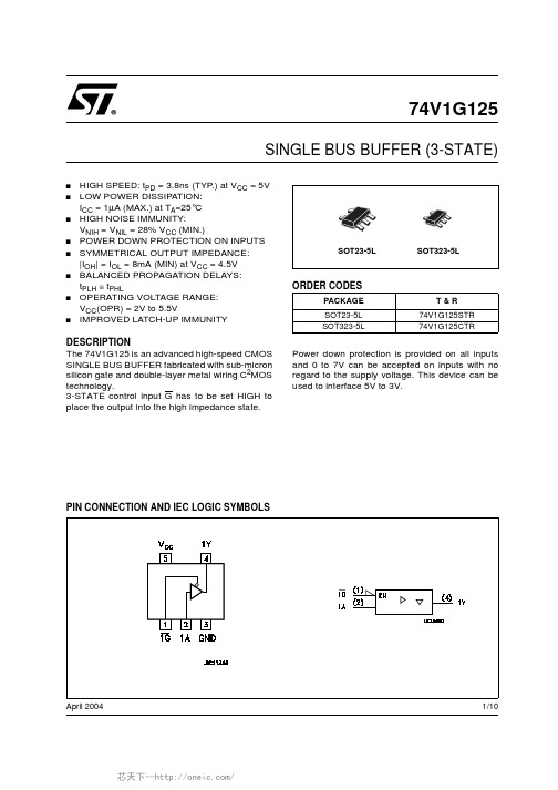
1/10April 2004s HIGH SPEED:t PD =3.8ns (TYP.)at V CC =5V sLOW POWER DISSIPATION:I CC =1µA (MAX.)at T A =25°C sHIGH NOISE IMMUNITY:V NIH =V NIL =28%V CC (MIN.)s POWER DOWN PROTECTION ON INPUTS sSYMMETRICAL OUTPUT IMPEDANCE:|I OH |=I OL =8mA (MIN)at V CC =4.5V sBALANCED PROPAGATION DELAYS:t PLH ≅t PHLsOPERATING VOLTAGE RANGE:V CC (OPR)=2V to 5.5VsIMPROVED LATCH-UP IMMUNITYDESCRIPTIONThe 74V1G125is an advanced high-speed CMOS SINGLE BUS BUFFER fabricated with sub-micron silicon gate and double-layer metal wiring C 2MOS technology.3-STATE control input G has to be set HIGH to place the output into the high impedance state.Power down protection is provided on all inputs and 0to 7V can be accepted on inputs with no regard to the supply voltage.This device can be used to interface 5V to 3V.74V1G125SINGLE BUS BUFFER(3-STATE)PIN CONNECTION AND IEC LOGIC SYMBOLSORDER CODESPACKAGE T &R SOT23-5L 74V1G125STR SOT323-5L74V1G125CTR74V1G1252/10INPUT EQUIVALENT CIRCUITPIN DESCRIPTIONTRUTH TABLEX :Don’t CareZ :High ImpedanceABSOLUTE MAXIMUM RATINGSAbsolute Maximum Ratings are those values beyond which damage to the device may occur.Functional operation under these conditions is not implied.RECOMMENDED OPERATING CONDITIONS1)V IN from 30%to 70%of V CCPIN N°SYMBOL NAME AND FUNCTION 11G Output Enable Input 21A Data Input 41Y Data Output 3GND Ground (0V)5V CCPositive Supply VoltageA G Y X H Z L L L HLHSymbol ParameterValue Unit V CC Supply Voltage -0.5to +7.0V V I DC Input Voltage -0.5to +7.0V V O DC Output Voltage -0.5to V CC +0.5V I IK DC Input Diode Current -20mA I OK DC Output Diode Current ±20mA I ODC Output Current±25mA I CC or I GND DC V CC or Ground Current±50mA T stg Storage Temperature-65to +150°C T LLead Temperature (10sec)260°CSymbol ParameterValue Unit V CC Supply Voltage 2to 5.5V V I Input Voltage 0to 5.5V V O Output Voltage 0to V CC V T op Operating Temperature-55to 125°C dt/dvInput Rise and Fall Time (note 1)(V CC =3.3±0.3V)(V CC =5.0±0.5V)0to 1000to 20ns/V ns/V74V1G1253/10DC SPECIFICATIONSAC ELECTRICAL CHARACTERISTICS (Input t r =t f =3ns)(*)Voltage range is 3.3V ±0.3V (**)Voltage range is 5.0V ±0.5VSymbolParameterTest ConditionValue UnitV CC (V)T A =25°C -40to 85°C -55to 125°C Min.Typ.Max.Min.Max.Min.Max.V IHHigh Level Input Voltage 2.0 1.5 1.5 1.5V3.0to 5.50.7V CC0.7V CC0.7V CCV ILLow Level Input Voltage2.00.50.50.5V3.0to 5.50.3V CC0.3V CC0.3V CCV OHHigh Level Output Voltage2.0I O =-50µA 1.9 2.0 1.9 1.9V3.0I O =-50µA 2.9 3.0 2.9 2.94.5I O =-50µA 4.4 4.54.4 4.43.0I O =-4mA 2.58 2.48 2.44.5I O =-8mA 3.943.83.7V OLLow Level Output Voltage2.0I O =50µA 0.00.10.10.1V3.0I O =50µA 0.00.10.10.14.5I O =50µA 0.00.10.10.13.0I O =4mA 0.360.440.554.5I O =8mA 0.360.440.55I OZ High Impedance Output Leakage Current5.5V I =V IH or V IL V O =V CC or GND ±0.25±2.5±5µA I I Input Leakage Current0to 5.5V I =5.5V or GND ±0.1±1±1µA I CCQuiescent Supply Current5.5V I =V CC or GND11020µA SymbolParameterTest ConditionValueUnitV CC (V)C L (pF)T A =25°C -40to 85°C -55to 125°C Min.Typ.Max.Min.Max.Min.Max.t PLH t PHLPropagation Delay Time3.3(*)15 5.17.5 1.08.5 1.09.5ns 3.3(*)50 5.68.0 1.09.5 1.010.55.0(**)15 3.8 5.5 1.0 6.5 1.07.55.0(**)50 4.3 6.5 1.07.5 1.08.5t PLZ t PHZOutput Disable Time3.3(*)15 5.48.0 1.09.0 1.010.0ns 3.3(*)507.911.5 1.012.5 1.013.55.0(**)15 3.6 5.0 1.0 6.0 1.07.05.0(**)50 5.17.0 1.08.0 1.09.0t PZL t PZHOutput Enable Time3.3(*)15 5.47.6 1.09.5 1.010.5ns 3.3(*)50 5.98.5 1.010.0 1.011.05.0(**)15 3.7 5.9 1.07.0 1.08.05.0(**)504.16.51.07.51.08.574V1G1254/10CAPACITIVE CHARACTERISTICS1)C PD is defined as the value of the IC’s internal equivalent capacitance which is calculated from the operating current consumption without load.(Refer to Test Circuit).Average operating current can be obtained by the following equation.I CC(opr)=C PD x V CC x f IN +I CCTEST CIRCUITCL =15/50pF or equivalent (includes jig and probe capacitance)R1=1K Ω or equivalentR T =Z OUT of pulse generator (typically 50Ω)SymbolParameterTest ConditionValue UnitT A =25°C -40to 85°C -55to 125°C Min.Typ.Max.Min.Max.Min.Max.C IN Input Capacitance 4101010pF C OUT OutputCapacitance4pF C PDPower Dissipation Capacitance (note 1)10pF TESTSWITCH t PLH ,t PHL Open t PZL ,t PLZ V CC t PZH ,t PHZGND74V1G1255/10WAVEFORM 1:PROPAGATION DELAYS (f=1MHz;50%duty cycle)WAVEFORM 2:OUTPUT ENABLE AND DISABLE TIME (f=1MHz;50%dutycycle)74V1G1258/1074V1G125Information furnished is believed to be accurate and reliable. However, STMicroelectronics assumes no responsibility for the consequences of use of such information nor for any infringement of patents or other rights of third parties which may result from its use. No license is granted by implication or otherwise under any patent or patent rights of STMicroelectronics. Specifications mentioned in this publication are subject to change without notice. This publication supersedes and replaces all information previously supplied. STMicroelectronics products are not authorized for use as critical components in life support devices or systems without express written approval of STMicroelectronics.The ST logo is a registered trademark of STMicroelectronicsAll other names are the property of their respective owners© 2004 STMicroelectronics - All Rights ReservedSTMicroelectronics GROUP OF COMPANIESAustralia - Belgium - Brazil - Canada - China - Czech Republic - Finland - France - Germany - Hong Kong - India - Israel - Italy - Japan - Malaysia - Malta - Morocco - Singapore - Spain - Sweden - Switzerland - United Kingdom - United States.10/10。
74系列功能大全(中文)

74系列功能大全(中文)74、74HC、74LS系列芯片资料,从网上下的,集合了一下系列电平典型传输延迟ns 最大驱动电流(-Ioh/Lol)mAAHC CMOS 8.5 -8/8AHCT COMS/TTL 8.5 -8/8HC COMS 25 -8/8HCT COMS/TTL 25 -8/8ACT COMS/TTL 10 -24/24F TTL 6.5 -15/64ALS TTL 10 -15/64LS TTL 18 -15/24注:同型号的74系列、74HC系列、74LS系列芯片,逻辑功能上是一样的。
74LSxx的使用说明如果找不到的话,可参阅74xx或74HCxx的使用说明。
有些资料里包含了几种芯片,如74HC161资料里包含了74HC160、74HC161、74HC162、74HC163四种芯片的资料。
找不到某种芯片的资料时,可试着查看一下临近型号的芯片资料。
7400 QUAD 2-INPUT NAND GATES 与非门7401 QUAD 2-INPUT NAND GATES OC 与非门7402 QUAD 2-INPUT NOR GATES 或非门7403 QUAD 2-INPUT NAND GATES 与非门7404 HEX INVERTING GATES 反向器7406 HEX INVERTING GATES HV 高输出反向器7408 QUAD 2-INPUT AND GATE 与门7409 QUAD 2-INPUT AND GATES OC 与门7410 TRIPLE 3-INPUT NAND GATES 与非门7411 TRIPLE 3-INPUT AND GATES 与门74121 ONE-SHOT WITH CLEAR 单稳态74132 SCHMITT TRIGGER NAND GATES 触发器与非门7414 SCHMITT TRIGGER INVERTERS 触发器反向器74153 4-LINE TO 1 LINE SELECTOR 四选一74155 2-LINE TO 4-LINE DECODER 译码器74180 PARITY GENERATOR/CHECKER 奇偶发生检验74191 4-BIT BINARY COUNTER UP/DOWN 计数器7420 DUAL 4-INPUT NAND GATES 双四输入与非门7426 QUAD 2-INPUT NAND GATES 与非门7427 TRIPLE 3-INPUT NOR GATES 三输入或非门7430 8-INPUT NAND GATES 八输入端与非门7432 QUAD 2-INPUT OR GATES 二输入或门7438 2-INPUT NAND GATE BUFFER 与非门缓冲器7445 BCD-DECIMAL DECODER/DRIVER BCD译码驱动器7474 D-TYPE FLIP-FLOP D型触发器7475 QUAD LATCHES 双锁存器7476 J-K FLIP-FLOP J-K触发器7485 4-BIT MAGNITUDE COMPARATOR 四位比较器7486 2-INPUT EXCLUSIVE OR GATES 双端异或门74HC00 QUAD 2-INPUT NAND GATES 双输入与非门74HC02 QUAD 2-INPUT NOR GATES 双输入或非门74HC03 2-INPUT OPEN-DRAIN NAND GATES 与非门74HC04 HEX INVERTERS 六路反向器74HC05 HEX INVERTERS OPEN DRAIN 六路反向器74HC08 2-INPUT AND GATES 双输入与门74HC107 J-K FLIP-FLOP WITH CLEAR J-K触发器74HC109A J-K FLIP-FLOP W/PRESET J-K触发器74HC11 TRIPLE 3-INPUT AND GATES 三输入与门74HC112 DUAL J-K FLIP-FLOP 双J-K触发器74HC113 DUAL J-K FLIP-FLOP PRESET 双JK触发器74HC123A RETRIGGERABLE MONOSTAB 可重触发单稳74HC125 TRI-STATE QUAD BUFFERS 四个三态门74HC126 TRI-STATE QUAD BUFFERS 六三态门74HC132 2-INPUT TRIGGER NAND 施密特触发与非门74HC133 13-INPUT NAND GATES 十三输入与非门74HC137 3-TO-8 DECODERS W/LATCHES 3-8线译码器74HC138 3-8 LINE DECODER 3线至8线译码器74HC139 2-4 LINE DECODER 2线至4线译码器74HC14 TRIGGERED HEX INVERTER 六触发反向器74HC147 10-4 LINE PRIORITY ENCODER 10-4编码器74HC148 8-3 LINE PRIORITY ENCODER 8-3编码器74HC149 8-8 LINE PRIORITY ENCODER 8-8编码器74HC151 8-CHANNEL DIGITAL MUX 8通道多路器74HC153 DUAL 4-INPUT MUX 双四输入多路器74HC154 4-16 LINE DECODER 4线至16线译码器74HC155 2-4 LINE DECODER 2线至4线译码器74HC157 QUAD 2-INPUT MUX 四个双端多路器74HC161 BINARY COUNTER 二进制计数器74HC163 DECADE COUNTERS 十进制计数器74HC164 SERIAL-PARALLEL SHIFT REG 串入并出74HC165 PARALLEL-SERIAL SHIFT REG 并入串出74HC166 SERIAL-PARALLEL SHIFT REG 串入并出74HC173 TRI-STATE D FLIP-FLOP 三态D触发器74HC174 HEX D FLIP-FLOP W/CLEAR 六D触发器74HC175 HEX D FLIP-FLOP W/CLEAR 六D触发器74HC181 ARITHMETIC LOGIC UNIT 算术逻辑单元74HC182 LOOK AHEAD CARRYGENERATR 进位发生器74HC190 BINARY UP/DN COUNTER 二进制加减计数器74HC191 DECADE UP/DN COUNTER 十进制加减计数器74HC192 DECADE UP/DN COUNTER 十进制加减计数器74HC193 BINARY UP/DN COUNTER 二进制加减计数器74HC194 4BIT BI-DIR SHIFT 4位双向移位寄存器74HC195 4BIT PARALLEL SHIFT 4位并行移位寄存器74HC20 QUAD 4-INPUT NAND GATE 四个四入与非门74HC221A NON-RETRIG MONOSTAB 不可重触发单稳74HC237 3-8 LINE DECODER 地址锁3线至8线译码器74HC242/243 TRI-STAT TRANSCEIVER 三态收发器74HC244 OCTAL 3-STATE BUFFER 八个三态缓冲门74HC245 OCTAL 3-STATE TRANSCEIVER 三态收发器74HC251 8-CH 3-STATE MUX 8路3态多路器74HC253 DUAL 4-CH 3-STATE MUX 4路3态多路器74HC257 QUAD 2-CH 3-STATE MUX 4路3态多路器74HC258 2-CH 3-STATE MUX 2路3态多路器74HC259 3-8 LINE DECODER 8位地址锁存译码器74HC266A 2-INPUT EXCLUSIVE NOR GATE 异或非74HC27 TRIPLE 3-INPUT NOR GATE三个3输入或非门74HC273 OCTAL D FLIP-FLOP CLEAR 8路D触发器74HC280 9BIT ODD/EVEN GENERATOR 奇偶发生器74HC283 4BIT BINARY ADDER CARRY 四位加法器74HC299 3-STATE UNIVERSAL SHIFT 三态移位寄存74HC30 8-INPUT NAND GATE 8输入端与非门74HC32 QUAD 2-INPUT OR GATE 四个双端或门74HC34 NON-INVERTER 非反向器74HC354 8-CH 3-STATE MUX 8路3态多路器74HC356 8-CH 3-STATE MUX 8路3态多路器74HC365 HEX 3-STATE BUFFER 六个三态缓冲门74HC366 3-STATE BUFFER INVERTER 缓冲反向器74HC367 3-STATE BUFFER INVERTER 缓冲反向器74HC368 3-STATE BUFFER INVERTER 缓冲反向器74HC373 3-STATE OCTAL D LATCHES 三态D型锁存器74HC374 3-STATE OCTAL D FLIPFLOP 三态D触发器74HC393 4-BIT BINARY COUNTER 4位二进制计数器74HC4016 QUAD ANALOG SWITCH 四路模拟量开关74HC4020 14-Stage Binary Counter 14输出计数器74HC4017 Decade Counter/Divider with 10 Decoded Outputs 十进制计数器带10个译码输出端74HC4040 12 Stage Binary Counter 12出计数器74HC4046 PHASE LOCK LOOP 相位监测输出器74HC4049 LEVEL DOWN CONVERTER 电平变低器74HC4050 LEVEL DOWN CONVERTER 电平变低器74HC4051 8-CH ANALOG MUX 8通道多路器74HC4052 4-CH ANALOG MUX 4通道多路器74HC4053 2-CH ANALOG MUX 2通道多路器74HC4060 14-STAGE BINARY COUNTER 14阶BIN计数74HC4066 QUAD ANALOG MUX 四通道多路器74HC4075 TRIPLE 3-INPUT OR GATE 3输入或门74HC42 BCD TO DECIMAL BCD转十进制译码器74HC423A RETRIGGERABLE MONOSTAB 可重触发单稳74HC4511 BCD-7 SEG DRIVER/DECODER 7段译码器74HC4514 4-16 LINE DECODER 4至16线译码器74HC4538A RETRIGGERAB MONOSTAB 可重触发单稳74HC4543 LCD BCD-7 SEG LCD用的BCD-7段译码驱动74HC51 AND OR GATE INVERTER 与或非门74HC521 8BIT MAGNITUDE COMPARATOR 判决定路74HC533 3-STATE D LATCH 三态D锁存器74HC534 3-STATE D FLIP-FLOP 三态D型触发器74HC540 3-STATE BUFFER 三态缓冲器74HC541 3-STATE BUFFER INVERTER三态缓冲反向器74HC58 DUAL AND OR GATE 与或门74HC589 3STATE 8BIT SHIFT 8位移位寄存三态输出74HC594 8BIT SHIFT REG 8位移位寄存器74HC595 8BIT SHIFT REG 8位移位寄存器出锁存74HC597 8BIT SHIFT REG 8位移位寄存器入锁存74HC620 3-STATE TRANSCEIVER 反向3态收发器74HC623 3-STATE TRANSCEIVER 八路三态收发器74HC640 3-STATE TRANSCEIVER 反向3态收发器74HC643 3-STATE TRANSCEIVER 八路三态收发器74HC646 NON-INVERT BUS TRANSCEIVER 总线收发器74HC648 INVERT BUS TRANCIVER 反向总线收发器74HC688 8BIT MAGNITUDE COMPARATOR 8位判决电路74HC7266 2-INPUT EXCLUSIVE NOR GATE 异或非门74HC73 DUAL J-K FLIP-FLOP W/CLEAR 双JK触发器74HC74A PRESET/CLEAR D FLIP-FLOP 双D触发器74HC75 4BIT BISTABLE LATCH 4位双稳锁存器74HC76 PRESET/CLEAR JK FLIP-FLOP 双JK触发器74HC85 4BIT MAGNITUDE COMPARATOR 4位判决电路74HC86 2INPUT EXCLUSIVE OR GATE 2输入异或门74HC942 BAUD MODEM 300BPS低速调制解调器74HC943 300 BAUD MODEM 300BPS低速调制解调器74LS00 QUAD 2-INPUT NAND GATES 与非门74LS02 QUAD 2-INPUT NOR GATES 或非门74LS03 QUAD 2-INPUT NAND GATES 与非门74LS04 HEX INVERTING GATES 反向器74LS05 HEX INVERTERS OPEN DRAIN 六路反向器74LS08 QUAD 2-INPUT AND GATE 与门74LS09 QUAD 2-INPUT AND GATES OC 与门74LS10 TRIPLE 3-INPUT NAND GATES 与非门74LS109 QUAD 2-INPUT AND GATES OC 与门74LS11 TRIPLE 3-INPUT AND GATES 与门74LS112 DUAL J-K FLIP-FLOP 双J-K触发器74LS113 DUAL J-K FLIP-FLOP PRESET 双JK触发器74LS114 NEGATIVE J-K FLIP-FLOP 负沿J-K触发器74LS122 Retriggerable Monostab 可重触发单稳74LS123 Retriggerable Monostable 可重触发单稳74LS125 TRI-STATE QUAD BUFFERS 四个三态门74LS13 QUAL 4-in NAND TRIGGER 4输入与非触发器74LS160 BCD DECADE 4BIT BIN COUNTERS 计数器74LS136 QUADRUPLE 2-INPUT XOR GATE 异或门74LS138 3-8 LINE DECODER 3线至8线译码器74LS139 2-4 LINE DECODER 2线至4线译码器74LS14 TRIGGERED HEX INVERTER 六触发反向器74HC147 10-4 LINE PRIORITY ENCODER 10-4编码器74HC148 8-3 LINE PRIORITY ENCODER 8-3编码器74HC149 8-8 LINE PRIORITY ENCODER 8-8编码器74LS151 8-CHANNEL DIGITAL MUX 8通道多路器74LS153 DUAL 4-INPUT MUX 双四输入多路器74LS155 2-4 LINE DECODER 2线至4线译码器74LS156 2-4 LINE DECODER/DEMUX 2-4译码器74LS157 QUAD 2-INPUT MUX 四个双端多路器74LS158 2-1 LINE MUX 2-1线多路器74LS160A BINARY COUNTER 二进制计数器74LS161A BINARY COUNTER 二进制计数器74LS162A BINARY COUNTER 二进制计数器74LS163A DECADE COUNTERS 十进制计数器74LS164 SERIAL-PARALLEL SHIFT REG 串入并出74LS168 BI-DIRECT BCD TO DECADE 双向计数器74LS169 4BIT UP/DN BIN COUNTER 四位加减计数器74LS173 TRI-STATE D FLIP-FLOP 三态D触发器74LS174 HEX D FLIP-FLOP W/CLEAR 六D触发器74LS175 HEX D FLIP-FLOP W/CLEAR 六D触发器74LS190 BINARY UP/DN COUNTER 二进制加减计数器74LS191 DECADE UP/DN COUNTER 十进制加减计数器74LS192 DECADE UP/DN COUNTER 十进制加减计数器74LS193 BINARY UP/DN COUNTER 二进制加减计数器74LS194A 4BIT BI-DIR SHIFT 4位双向移位寄存器74LS195A 4BIT PARALLEL SHIFT4位并行移位寄存器74LS20 QUAD 4-INPUT NAND GATE 四个四入与非门74LS21 4-INPUT AND GATE 四输入端与门74LS240 OCTAL 3-STATE BUFFER 八个三态缓冲门74LS244 OCTAL 3-STATE BUFFER 八个三态缓冲门74LS245 OCTAL 3-STATE TRANSCEIVER 三态收发器74LS253 DUAL 4-CH 3-STATE MUX 4路3态多路器74LS256 4BIT ADDRESS LATCH 四位可锁存锁存器74LS257 QUAD 2-CH 3-STATE MUX 4路3态多路器74LS258 2-CH 3-STATE MUX 2路3态多路器74LS27 TRIPLE 3-INPUT NOR GATES 三输入或非门74LS279 QUAD R-S LATCHES 四个RS非锁存器74LS28 QUAD 2-INPUT NOR BUFFER 四双端或非缓冲74LS283 4BIT BINARY ADDER CARRY 四位加法器74LS30 8-INPUT NAND GATES 八输入端与非门74LS32 QUAD 2-INPUT OR GATES 二输入或门74LS352 4-1 LINE SELECTOR/MUX 4-1线选择多路器74LS365 HEX 3-STATE BUFFER 六个三态缓冲门74LS367 3-STATE BUFFER INVERTER 缓冲反向器74LS368A 3-STATE BUFFER INVERTER 缓冲反向器74LS373 OCT LATCH W/3-STATE OUT三态输出锁存器74LS76 Dual JK Flip-Flop w/set 2个JK触发器74LS379 QUAD PARALLEL REG 四个并行寄存器74LS38 2-INPUT NAND GATE BUFFER 与非门缓冲器74LS390 DUAL DECADE COUNTER 2个10进制计数器74LS393 DUAL BINARY COUNTER 2个2进制计数器74LS42 BCD TO DECIMAL BCD转十进制译码器74LS48 BCD-7 SEG BCD-7段译码器74LS49 BCD-7 SEG BCD-7段译码器74LS51 AND OR GATE INVERTER 与或非门74LS540 OCT Buffer/Line Driver 8路缓冲驱动器74LS541 OCT Buffer/LineDriver 8路缓冲驱动器74LS74 D-TYPE FLIP-FLOP D型触发器74LS682 8BIT MAGNITUDE COMPARATOR 8路比较器74LS684 8BIT MAGNITUDE COMPARATOR 8路比较器74LS75 QUAD LATCHES 双锁存器74LS83A 4BIT BINARY ADDER CARRY 四位加法器74LS85 4BIT MAGNITUDE COMPARAT 4位判决电路74LS86 2INPUT EXCLUSIVE OR GATE 2输入异或门74LS90 DECADE/BINARY COUNTER 十/二进制计数器74LS95B 4BIT RIGHT/LEFT SHIFT 4位左右移位寄存74LS688 8BIT MAGNITUDE COMPARAT 8位判决电路74LS136 2-INPUT XOR GATE 2输入异或门74LS651 BUS TRANSCEIVERS 总线收发器74LS653 BUS TRANSCEIVERS 总线收发器74LS670 3-STATE 4-BY-4 REG 3态4-4寄存器74LS73A DUAL J-K FLIP-FLOP W/CLEAR 双JK触发器。
SL74HCT14资料
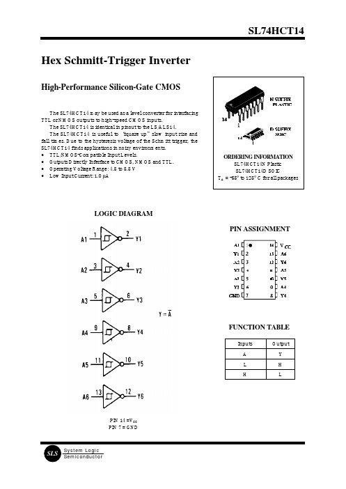
Min 4.5 0 -55 0
Max 5.5 VCC +125 No Limit*
Unit V V °C ns
When VIN ≈ 50% VCC ,ICC>1.0 mA.
This device contains protection circuitry to guard against damage due to high static voltages or electric fields. However, precautions must be taken to avoid applications of any voltage higher than maximum rated voltages to this high-impedance circuit. For proper operation, VIN and VOUT should be constrained to the range GND≤(VIN or VOUT)≤VCC. Unused inputs must always be tied to an appropriate logic voltage level (e.g., either GND or VCC). Unused outputs must be left open.
元器件交易网
SL74HCT14
Hex Schmitt-Trigger Inverter
High-Performance Silicon-Gate CMOS
The SL74HCT14 may be used as a level converter for interfacing TTL or NMOS outputs to high-speed CMOS inputs. The SL74HCT14 is identical in pinout to the LS/ALS14. The SL74HCT14 is useful to “square up” slow input rise and fall times. Due to the hysteresis voltage of the Schmitt trigger, the SL74HCT14 finds applications in noisy environments. • TTL/NMOS-Compatible Input Levels. • Outputs Directly Inferface to CMOS, NMOS and TTL. • Operating Voltage Range: 4.5 to 5.5 V • Low Input Current: 1.0 µA
MC74VHC1GT14中文资料
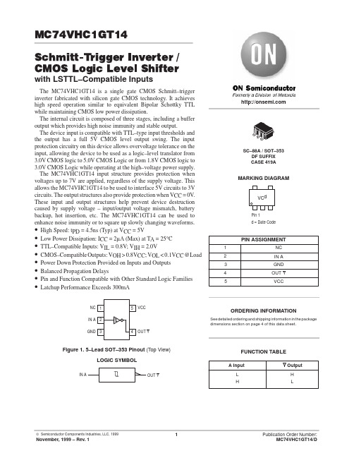
PIN ASSIGNMENT123GND NC IN A 45VCCOUT YUSA/EUROPE Literature Fulfillment :Literature Distribution Center for ON Semiconductor P .O. Box 5163, Denver, Colorado 80217 USAPhone : 303–675–2175 or 800–344–3860 Toll Free USA/Canada Fax : 303–675–2176 or 800–344–3867 Toll Free USA/Canada Email : ONlit@Fax Response Line *:303–675–2167800–344–3810 Toll Free USA/Canada*To receive a Fax of our publicationsON Semiconductor and are trademarks of Semiconductor Components Industries, LLC (SCILLC). SCILLC reserves the right to make changes without further notice to any products herein. SCILLC makes no warranty, representation or guarantee regarding the suitability of its products for any particular purpose, nor does SCILLC assume any liability arising out of the application or use of any product or circuit, and specifically disclaims any and all liability,including without limitation special, consequential or incidental damages. “Typical” parameters which may be provided in SCILLC data sheets and/or specifications can and do vary in different applications and actual performance may vary over time. All operating parameters, including “Typicals” must be validated for each customer application by customer’s technical experts. SCILLC does not convey any license under its patent rights nor the rights of others.SCILLC products are not designed, intended, or authorized for use as components in systems intended for surgical implant into the body, or other applications intended to support or sustain life, or for any other application in which the failure of the SCILLC product could create a situation where personal injury or death may occur. Should Buyer purchase or use SCILLC products for any such unintended or unauthorized application, Buyer shall indemnify and hold SCILLC and its officers, employees, subsidiaries, affiliates, and distributors harmless against all claims, costs, damages, and expenses, and reasonable attorney fees arising out of, directly or indirectly, any claim of personal injury or death associated with such unintended or unauthorized use, even if such claim alleges that SCILLC was negligent regarding the design or manufacture of the part. SCILLC is an Equal Opportunity/Affirmative Action Employer.PUBLICATION ORDERING INFORMATIONASIA/PACIFIC : LDC for ON Semiconductor – Asia SupportPhone :303–675–2121 (Tue–Fri 9:00am to 1:00pm, Hong Kong Time)Email : ONlit–asia@JAPAN : ON Semiconductor, Japan Customer Focus Center4–32–1 Nishi–Gotanda, Shinagawa–ku, Tokyo, Japan 141–8549Phone : 81–3–5487–8345Email : r14153@ON Semiconductor Website: 。
- 1、下载文档前请自行甄别文档内容的完整性,平台不提供额外的编辑、内容补充、找答案等附加服务。
- 2、"仅部分预览"的文档,不可在线预览部分如存在完整性等问题,可反馈申请退款(可完整预览的文档不适用该条件!)。
- 3、如文档侵犯您的权益,请联系客服反馈,我们会尽快为您处理(人工客服工作时间:9:00-18:30)。
1/9April 2004s HIGH SPEED:t PD =5.0ns (TYP.)at V CC =5V sLOW POWER DISSIPATION:I CC =1µA(MAX.)at T A =25°C sTYPICAL HYSTERESIS:V h =700mV at V CC =4.5Vs POWER DOWN PROTECTION ON INPUT sSYMMETRICAL OUTPUT IMPEDANCE:|I OH |=I OL =8mA (MIN)at V CC =4.5V sBALANCED PROPAGATION DELAYS:t PLH ≅t PHLsOPERATING VOLTAGE RANGE:V CC (OPR)=4.5V to 5.5VsIMPROVED LATCH-UP IMMUNITYDESCRIPTIONThe 74V1T14is an advanced high-speed CMOS SINGLE SCHMITT INVERTER fabricated with sub-micron silicon gate and double-layer metal wiring C 2MOS technology.The internal circuit is composed of 3stages including buffer output,which provide high noise immunity and stable output.Power down protection is provided on input and 0to 7V can be accepted on input with no regard to the supply voltage.This device can be used tointerface 5V to 3V.Pin configuration and function are the same as those of the 74V1T04but the 74V1T14has hysteresis.This together with its schmitt trigger function allows it to be used on line receivers with slow rise/fall input signals.The input is equipped with protection circuits against static discharge,giving it ESD immunity and transient excess voltage.74V1T14SINGLE SCHMITTINVERTERPIN CONNECTION AND IEC LOGIC SYMBOLSORDER CODESPACKAGE T &R SOT23-5L 74V1T14STR SOT323-5L74V1T14CTR74V1T142/9INPUT EQUIVALENT CIRCUITPIN DESCRIPTIONTRUTH TABLEABSOLUTE MAXIMUM RATINGSAbsolute Maximum Ratings are those values beyond which damage to the device may occur.Functional operation under these conditions isnot implied.RECOMMENDED OPERATING CONDITIONSPIN N°SYMBOL NAME AND FUNCTION 1NC Not Connected 21A Data Input 41Y Data Output 3GND Ground (0V)5V CCPositive Supply VoltageA Y L H HLSymbol ParameterValue Unit V CC Supply Voltage -0.5to +7.0V V I DC Input Voltage -0.5to +7.0V V O DC Output Voltage -0.5to V CC +0.5V I IK DC Input Diode Current -20mA I OK DC Output Diode Current ±20mA I ODC Output Current±25mA I CC or I GND DC V CC or Ground Current±50mA T stgStorage Temperature -65to +150°C T LLead Temperature (10sec)260°CSymbol ParameterValue Unit V CC Supply Voltage 4.5to 5.5V V I Input Voltage 0to 5.5V V O Output Voltage 0to V CC V T opOperating Temperature-55to 125°C74V1T143/9DC SPECIFICATIONSAC ELECTRICAL CHARACTERISTICS (Input t r =t f =3ns)(*)Voltage range is 5.0V ±0.5VCAPACITIVE CHARACTERISTICS1)C PD is defined as the value of the IC’s internal equivalent capacitance which is calculated from the operating current consumption without load.(Refer to Test Circuit).Average operating current can be obtained by the following equation.I CC(opr)=C PD x V CC x f IN +I CCSymbolParameterTest ConditionValue UnitV CC (V)T A =25°C -40to 85°C -55to 125°C Min.Typ.Max.Min.Max.Min.Max.V t+High LevelThreshold Voltage 4.50.9 2.00.9 2.00.9 2.0V 5.5 1.1 2.0 1.1 2.0 1.1 2.0V t-Low LevelThreshold Voltage 4.50.5 1.50.5 1.50.5 1.5V 5.50.6 1.60.6 1.60.6 1.6V h Hysteresis Voltage 4.50.4 1.40.4 1.40.4 1.4V 5.50.5 1.60.5 1.60.5 1.6V OH High Level Output Voltage4.5I O =-50µA 4.4 4.54.4 4.4V 4.5I O =-8mA 3.943.83.7V OL Low Level Output Voltage4.5I O =50µA 0.00.10.10.1V4.5I O =8mA 0.360.440.55I I Input Leakage Current0to 5.5V I =5.5V or GND ±0.1±1.0±1.0µA I CC Quiescent Supply Current5.5V I =V CC or GND 11020µA +I CCAdditional Worst Case Supply Current5.5One Input at 3.4V,other input at V CCor GND1.351.5 1.5mA SymbolParameterTest ConditionValue UnitV CC (V)C L (pF)T A =25°C -40to 85°C -55to 125°C Min.Typ.Max.Min.Max.Min.Max.t PLH t PHLPropagation Delay Time5.0(*)15 5.07.5 1.09.0 1.010.5ns 5.0(*)506.58.51.010.01.011.5SymbolParameterTest ConditionValue UnitT A =25°C -40to 85°C -55to 125°C Min.Typ.Max.Min.Max.Min.Max.C IN Input Capacitance 4101010pF C PDPower Dissipation Capacitance (note 1)14pF74V1T144/9TEST CIRCUITL R T =Z OUT of pulse generator (typically 50Ω)WAVEFORM:PROPAGATION DELAY (f=1MHz;50%dutycycle)74V1T147/974V1T14 Information furnished is believed to be accurate and reliable. However, STMicroelectronics assumes no responsibility for the consequences of use of such information nor for any infringement of patents or other rights of third parties which may result from its use. No license is granted by implication or otherwise under any patent or patent rights of STMicroelectronics. Specifications mentioned in this publication are subject to change without notice. This publication supersedes and replaces all information previously supplied. STMicroelectronics products are not authorized for use as critical components in life support devices or systems without express written approval of STMicroelectronics.The ST logo is a registered trademark of STMicroelectronicsAll other names are the property of their respective owners© 2004 STMicroelectronics - All Rights ReservedSTMicroelectronics GROUP OF COMPANIESAustralia - Belgium - Brazil - Canada - China - Czech Republic - Finland - France - Germany - Hong Kong - India - Israel - Italy - Japan - Malaysia - Malta - Morocco - Singapore - Spain - Sweden - Switzerland - United Kingdom - United States.9/9。
