lec6_7 Image Enhencement in Frequency Domain
ICH-Q7a(中英文对照)

Q7a(中英文对照)FDA原料药GMP指南Table of Contents 目录1. INTRODUCTION 1. 简介1.1 Objective 1.1目的1.2 Regulatory Applicability 1.2法规的适用性1.3 Scope 1.3范围2. QUALITY MANAGEMENT 2.质量管理2.1 Principles 2.1总则2.2 Responsibilities of the Quality Unit(s) 2.2质量部门的责任2.3 Responsibility for Production Activities 2.3生产作业的职责2.4 Internal Audits (Self Inspection) 2.4内部审计(自检)2.5 Product Quality Review 2.5产品质量审核3. PERSONNEL 3. 人员3.1 Personnel Qualifications 3.人员的资质3.2 Personnel Hygiene 3.2 人员卫生3.3 Consultants 3.3 顾问4. BUILDINGS AND FACILITIES 4. 建筑和设施4.1 Design and Construction 4.1 设计和结构4.2 Utilities 4.2 公用设施4.3 Water 4.3 水4.4 Containment 4.4 限制4.5 Lighting 4.5 照明4.6 Sewage and Refuse 4.6 排污和垃圾4.7 Sanitation and Maintenance 4.7 卫生和保养5. PROCESS EQUIPMENT 5. 工艺设备5.1 Design and Construction 5.1 设计和结构5.2 Equipment Maintenance and Cleaning 5.2 设备保养和清洁5.3 Calibration 5.3 校验5.4 Computerized Systems5.4 计算机控制系统6. DOCUMENTATION AND RECORDS6. 文件和记录 6.1 Documentation System andSpecifications6.1 文件系统和质量标准 6.2 Equipment cleaning and Use Record6.2 设备的清洁和使用记录 6.3 Records of Raw Materials,Intermediates, API Labeling and Packaging Materials6.3 原料、中间体、原料药的标签和包装材料的记录 6.4 Master Production Instructions (Master Production and Control Records)6.4 生产工艺规程(主生产和控制记录) 6.5 Batch Production Records (Batch Production and Control Records)6.5 批生产记录(批生产和控制记录) 6.6 Laboratory Control Records6.6 实验室控制记录 6.7 Batch Production Record Review6.7批生产记录审核7. MATERIALS MANAGEMENT7. 物料管理 7.1 General Controls7.1 控制通则 7.2 Receipt and Quarantine7.2接收和待验 7.3 Sampling and Testing of Incoming Production Materials7.3 进厂物料的取样与测试 7.4 Storage7.4储存 7.5 Re-evaluation7.5复验8. PRODUCTION AND IN-PROCESS CONTROLS8. 生产和过程控制 8.1 Production Operations8.1 生产操作 8.2 Time Limits8.2 时限 8.3 In-process Sampling and Controls8.3 工序取样和控制 8.4 Blending Batches of Intermediates or APIs8.4 中间体或原料药的混批 8.5 Contamination Control8.5 污染控制9. PACKAGING AND IDENTIFICATION LABELING OF APIs AND INTERMEDIATES9. 原料药和中间体的包装和贴签 9.1 General9.1 总则 9.2 Packaging Materials9.2 包装材料 9.3 Label Issuance and Control9.3 标签发放与控制 9.4 Packaging and Labeling Operations9.4 包装和贴签操作10. STORAGE AND DISTRIBUTION10.储存和分发 10.1 Warehousing Procedures10.1 入库程序 10.2 Distribution Procedures10.2 分发程序11. LABORATORY CONTROLS11.实验室控制 11.1 General Controls11.1 控制通则 11.2 Testing of Intermediates and APIs11.2 中间体和原料药的测试 11.3 Validation of Analytical Procedures11.3 分析方法的验证 11.4 Certificates of Analysis11.4 分析报告单 11.5 Stability Monitoring of APIs11.5 原料药的稳定性监测 11.6 Expiry and Retest Dating11.6 有效期和复验期 11.7 Reserve/Retention Samples11.7 留样12. V ALIDATION12.验证 12.1 Validation Policy12.1 验证方针 12.2 Validation Documentation12.2 验证文件 12.3 Qualification12.3 确认 12.4 Approaches to Process Validation12.4 工艺验证的方法 12.5 Process Validation Program12.5 工艺验证的程序 12.6 Periodic Review of Validated Systems12.6验证系统的定期审核 12.7 Cleaning Validation12.7 清洗验证 12.8 Validation of Analytical Methods12.8 分析方法的验证13. CHANGE CONTROL13.变更的控制14. REJECTION AND RE-USE OFMATERIALS14.拒收和物料的再利用 14.1 Rejection14.1 拒收 14.2 Reprocessing14.2 返工 14.3 Reworking14.3 重新加工 14.4 Recovery of Materials and Solvents14.4 物料与溶剂的回收 14.5 Returns14.5 退货15. COMPLAINTS AND RECALLS15.投诉与召回16. CONTRACT MANUFACTURERS(INCLUDING LABORATORIES)16.协议生产商(包括实验室)17. AGENTS, BROKERS, TRADERS, DISTRIBUTORS, REPACKERS, ANDRELABELLERS17.代理商、经纪人、贸易商、经销商、重新包装者和重新贴签者 17.1 Applicability17.1适用性 17.2 Traceability of Distributed APIs and Intermediates17.2已分发的原料药和中间体的可追溯性 17.3 Quality Management17.3质量管理 17.4 Repackaging, Relabeling, and Holding of APIs and Intermediates17.4原料药和中间体的重新包装、重新贴签和待检17.5 Stability17.5稳定性 17.6 Transfer of Information17.6 信息的传达 17.7 Handling of Complaints and Recalls17.7 投诉和召回的处理 17.8 Handling of Returns17.8 退货的处理18. Specific Guidance for APIsManufactured by Cell Culture/Fermentation 18. 用细胞繁殖/发酵生产的原料药的特殊指南18.1 General18.1 总则 18.2 Cell Bank Maintenance and Record Keeping18.2细胞库的维护和记录的保存 18.3 Cell Culture/Fermentation18.3细胞繁殖/发酵 18.4 Harvesting, Isolation and Purification18.4收取、分离和精制 18.5 Viral Removal/Inactivation steps18.5 病毒的去除/灭活步骤19. APIs for Use in Clinical Trials19. 用于临床研究的原料药 19.1 General19.1 总则 19.2 Quality19.2 质量 19.3 Equipment and Facilities19.3 设备和设施 19.4 Control of Raw Materials19.4 原料的控制 19.5 Production19.5 生产 19.6 Validation19.6 验证 19.7 Changes19.7 变更 19.8 Laboratory Controls19.8 实验室控制 19.9 Documentation19.9 文件20. Glossary20. 术语Q7a GMP Guidance for APIsQ7a 原料药的GMP 指南1. INTRODUCTION1. 简介 1.1 Objective1.1目的 This document is intended to provide guidance regarding good manufacturing practice (GMP) for the manufacturing of active pharmaceutical ingredients (APIs) under an appropriate system for managing quality. It is also intended to help ensure that APIs meet the quality and purity characteristics that they purport, or are represented, to possess. 本文件旨在为在合适的质量管理体系下制造活性药用成分(以下称原料药)提供有关优良药品生产管理规范(GMP )提供指南。
10.噪声系数分析仪(NFA)

Rg
P no
Rg (2900 K ) vg
ve2
无噪网络
G pm
2 v 实际网络 (T0 = 290 K ) 用一无噪声网络和一噪声源 e 等效。 2 设 ve 是由信号源内阻R g 在一假想温度Te 下产生的噪声电压。
v e2 = 4 KT e R g ∆ f
此温度 T e 是网络的等效噪声温度。
当噪声源中的二极管没有偏置时,只有噪声源中的衰减器产生的 热噪声,称为“冷态”; 当二极管有反向偏置并进入雪崩状态时,噪声大大增加,称为 “热态”。
Agilent提供的SNS系列噪声源指标如下图所示。
噪声源(续1)
噪声信号源的超噪比ENR(Excess Noise Ratio)的定义:
or ( ENR ) dB = 10 lg [(TSON − TSOFF ) / T0 ]
10.3.1 噪声源
大多数通用的噪声源是采用低结电容的二极管,当二极 管反向偏置并进入雪崩状态时,二极管产生的噪声是常 数。 精密噪声源(例如:Agilent的SNS系列)的输出端加入 衰减器,以降低SWR,减少测量中失配带来的误差。 利用噪声源的两种状态(on和off)可以测量噪声系数。
上式说明:级联网络的噪声系数,主要由网络前级的噪声系 数确定。前级的噪声系数越小,功率增益越高,则级联网络 的噪声系数就越小。
网络的噪声性能也可以用噪声温度来表示。但要注意的是, 网络的噪声温度不是该网络的实际物理温度,而是用以表征 该网络噪声性能的一种假想温度。
噪声温度
实际网络
vg G pm , PnA
ENR = (TSON − TSOFF ) / T0
噪声源(续2)
TECHKON说明书

Your TECHKON Team
Contents
Chapter 1: General description of the measurement system 1.1 Product description. .............................................................................. 5 1.2 Packing list ...........................................................................................2 4.3 4.4 4.5 4.6 4.7 4.8 4.9
Welcome We welcome you among the worldwide community of users of TECHKON products. We are happy that you have selected this high-quality measurement instrument. It will be a valuable tool for your day-to-day quality control tasks. With this manual we invite you to learn how to use SpectroDrive, the software ExPresso 3 and SpectroConnect. The manual is divided into four chapters: Chapter 1: Chapter 2: Chapter 3: Chapter 4: General description of the measurement system Installation of SpectroDrive and the software ExPresso 3 How to use SpectroDrive and the software ExPresso 3 How to use the Windows software SpectroConnect
Eu配合物 Efficient two-photon-sensitized luminescence
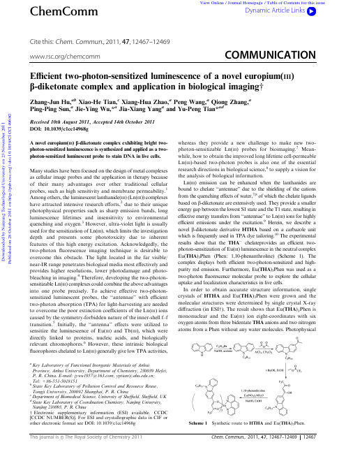
Cite this:mun .,2011,47,12467–12469Efficient two-photon-sensitized luminescence of a novel europium(III )b -diketonate complex and application in biological imaging wZhang-Jun Hu,ab Xiao-He Tian,c Xiang-Hua Zhao,a Peng Wang,a Qiong Zhang,a Ping-Ping Sun,a Jie-Ying Wu,*a Jia-Xiang Yang a and Yu-Peng Tian*adReceived 10th August 2011,Accepted 14th October 2011DOI:10.1039/c1cc14968gA novel europium(III )b -diketonate complex exhibiting bright two-photon-sensitized luminescence is synthesized and applied as a two-photon-sensitized luminescent probe to stain DNA in live cells.Many studies have been focused on the design of metal complexes as cellular image probes and the application in therapy because of their many advantages over other traditional cellular probes,such as high sensitivity and membrane permeability.1Among others,the luminescent lanthanide(III )(Ln(III ))complexes have attracted intensive research efforts,2due to their unique photophysical properties such as sharp emission bands,long luminescence lifetimes and insensitivity to environmental quenching and oxygen.3However,ultra-violet light is usually used for the sensitization of Ln(III ),which limits the investigation depth and presents some phototoxicity due to inherent features of this high energy excitation.Acknowledgedly,the two-photon fluorescence imaging technique is desirable to overcome this obstacle.The light located in the far visible/near-IR range penetrates biological media most effectively and provides higher resolutions,lower photodamage and photo-bleaching in imaging.4Therefore,developing the two-photon-sensitizable Ln(III )complexes could combine the above advantages into one probe precisely.To achieve effective two-photon-sensitized luminescent probes,the ‘‘antennae’’with efficient two-photon absorption (TPA)for light-harvesting are needed to overcome the poor extinction coefficients of the Ln(III )ions caused by the symmetry-forbidden nature of the inner-shell f–f transition.5Initially,the ‘‘antenna’’effects were utilized to sensitize the luminescence of Eu(III )and Tb(III ),which were directly linked to proteins,nucleic acids,and biologically relevant chromophores.6However,these intrinsic biological fluorophores chelated to Ln(III )generally give low TPA activities,whereas they provide a new challenge to make new two-photon-sensitizable Ln(III )probes for bioimaging.7Mean-while,how to obtain the improved long lifetime cell-permeable Ln(III )-based two-photon probes is also one of the essential research directions in biological science,8to supply a vision for the analysis of biological information.Ln(III )emission can be enhanced when the lanthanides are bound to chelate ‘‘antennae’’due to the shielding of the cations from the quenching effects of water,7,8of which the chelate ligands based on b -diketonate are extensively used.They provide a smaller energy gap between the lowest S1state and the T1state,resulting in effective energy transfers from ‘‘antennae’’to Ln(III )ions for highly efficient emissions under the excitation.9Herein,we describe a novel b -diketonate derivative HTHA based on a carbazole unit which is frequently used in TPA dye tailoring.10The experimental results show that the THA Àchelateprovides an efficient two-photon-sensitization of Eu(III )luminescence in the neutral complex Eu(THA )3Phen (Phen:1,10-phenanthroline)(Scheme 1).The complex displays both efficient two-photon-sensitized and high-purity red emission.Furthermore,Eu(THA )3Phen was used as a two-photon fluorescence molecular probe to explore the cellular uptake and localization characteristics in live cells.In order to obtain accurate structure information,single crystals of HTHA and Eu(THA )3Phen were grown and the molecular structures were determined by single crystal X-ray diffraction (in ESI w ).The result shows that Eu(THA )3Phen is mononuclear and the Eu(III )ion eight-coordinates with six oxygen atoms from three bidentate THA anions and two nitrogen atoms from a Phen without any water molecules.PhotophysicalaKey Laboratory of Functional Inorganic Materials of AnhuiProvince,Anhui University,Department of Chemistry,230039Hefei,P.R.China.E-mail:jywu1957@,yptian@;Tel:+86-551-5018151bState Key Laboratory of Pollution Control and Resource Reuse,Tongji University,200092Shanghai,P.R.China cDepartment of Biomedical Science,University of Sheffield,Sheffield,UK dState Key Laboratory of Coordination Chemistry,Nanjing University,Nanjing 210093,P.R.Chinaw Electronic supplementary information (ESI)DC [CCDC NUMBER(S)].For ESI and crystallographic data in CIF or other electronic format see DOI:10.1039/c1cc14968gChemCommDynamic Article Links/chemcommCOMMUNICATIOND o w n l o a d e d b y N a n y a n g T e c h n o l o g i c a l U n i v e r s i t y o n 23 N o v e m b e r 2011P u b l i s h e d o n 28 O c t o b e r 2011 o n h t t p ://p u b s .r s c .o r g | d o i :10.1039/C 1C C 14968GView Online / Journal Homepage / Table of Contents for this issuedata for HTHA and Eu(THA )3Phen are provided in Table 1.As shown in Fig.1a,HTHA mainly presents a broad absorption band centered at 360nm and a shoulder around 278nm in absorption spectra.The TD-DFT {[6-31G(d)]}calculations (Fig.2)indicate that the low energy transition presents marked charge transfer (CT)character,with the HOMO and the LUMO being mainly located on the carbazole donor and trifluoro-methane acceptor parts of the molecule,respectively.The most intense transition (367.8nm)arises from HOMO -LUMO and HOMO À1-LUMO transition,it has a p –p *character.The 4.23eV (293.4nm)transitions receive contributions from excitations involving several molecular orbitals,with a predominant weight of excitations from HOMO À1,HOMO À2and HOMO toward LUMO and LUMO À1.These transitions are assigned to two classes of transitions.One corresponds mainly to CT transition from the alkyl group to the p -conjugated bridge part,the other one can arise from a locally excited (LE)transition as monoelectronic transition localized in the p -conjugated plexation to Eu(III )results in a slight shift of the CT transition,which shows that the lanthanide Lewis acidity effect is partially compensated by the tris-anionic nature of the complex.As shown in Fig.1a,the spectral shapes of the complex are similar to HTHA ,indicating that the coordination of the Eu(III )does not significantly influence the energy of the singlet state of the b -diketone ligand.11Furthermore,it is accompanied by a threefold escalation of the extinction coefficient of low energy transition.Upon excitation of Eu(THA )3Phen at 364nm (CT band of the ligand),the characteristic bright-red long-livedluminescence of Eu(III )is observed,confirming that energy transfer takes place from the THA anions to Eu(III ).As shown in Fig.1b,the bands at lower energy are the emission bands of Eu(III ),which are typical of europium centered transitions from the 5D 0levels to the lower 7F 0–4levels of the ground-state multiplet.The sharp emission at 613nm corresponds to the hypersensitive transition of 5D 0-7F 2,which is forbidden as an electric dipole for Eu(III )in the strict D 4d symmetry.The Eu(III )cation factually has a geometrical environment between a square antiprism and a dodecahedron (in ESI w ).12This coordi-nation configuration around Eu(III )leads to a low structural symmetry.In addition,other important factors cannot be ignored,such as the aromatic electronic clouds and polarization effects 13caused by strong bonding of Eu(III )to the three THA Àand the disorders in the crystal.14They may also result in the effective crystal electric field symmetry at the Eu(III )site being lower than the ca.D 4d adopted by the coordination polyhedron or trigger 5D 0-7F 2transition.13Notably,it is found that the intensity of the short-wavelength emission (B 440nm)from the THA anions nearly disappears and 5D 0-7F 0–4are well resolved when excited in the solid state,which means that only a minute fraction of the energy of the THA anions is given out as their own emissions rather than transferred to Eu(III ).It can be presumed that the presence of solvent oscillators in solution could well serve to affect the local symmetry of the Eu(III )site or deactivate the ligand and Eu(III )excited states,so that the energy transfer to Eu(III )becomes less efficient.15The luminescent quantum yield is rather modest (0.08)at room temperature,however,due to the emission being concentrated in the hypersensitive D J =2narrow band (613nm),the emitted red light is still intense.The measured 5D 0-7F 2luminescence decays of Eu(THA )3Phen can be described by monoexponential kinetics and the measured luminescence lifetime (t )is 678m s at room temperature,which matches the need of long lifetime sensor systems.The excitation-energy dependence of integrated emission for HTHA and Eu(THA )3Phen are present in a logarithmic scale,respectively (Fig.S3,in ESI w ).In both cases,the experimental points fit nicely to a linear relationship with similar slopes of 2.06Æ0.03and 2.09Æ0.04,respectively.These values indicate that the emissions (Fig.1d)arise from a two-photon process.TheTable 1Photophysical data for HTHA and Eu(THA )3Phen measured at room temperature in dichloromethane (DCM)Compound l a e b Â104l c F d t e s f HTHA360 2.374490.36 4.19ns —Eu(THA )3Phen3646.576130.08678m s80al max of the maximum linear absorption spectra in nm.b The molar absorption coefficient in L mol À1cm À1.c l max of the emission spectra in nm.d Fluorescence quantum yield (Æ15%).e Luminescence life-time (Æ5%).f Maximum TPA cross-section in GM (at 720nm).Fig.1(a)Absorption spectra of HTHA and Eu(THA )3Phen in DCM (1Â10À5mol L À1);(b)photoluminescence spectra of Eu(THA )3Phen in DCM and solid sate (insets:photographs of solid powder and solution of Eu(THA )3Phen under UV light (365nm));(c)TPA cross sections (s )for Eu(THA )3Phen;(d)Two-photon-excited fluorescence of HTHA and two-photon-sensitized luminescence of Eu(THA )3Phen in DCM (1Â10À3mol L À1).Fig.2TD-DFT computed frontier orbitals of HTHA obtained at the B3LYP level.D o w n l o a d e d b y N a n y a n g T e c h n o l o g i c a l U n i v e r s i t y o n 23 N o v e m b e r 2011P u b l i s h e d o n 28 O c t o b e r 2011 o n h t t p ://p u b s .r s c .o r g | d o i :10.1039/C 1C C 14968Gexcitation power dependence was examined for 700–810nm and used in the subsequent determination of the TPA cross-sections (s ),which shows that the Eu(THA )3Phen is considered to have high efficiency in two-photon sensitization (Fig.1c).The maximum s value is estimated to be 80GM at 720nm,which is comparable to that of the two-photon-sensitized luminescent Eu(III )complex reported.7a –f Notably,the experimental points of TPA spectra agree with the wavelength-doubled linear absorption spectra of HTHA ,which indicates that the sensitized lumines-cence at 614nm is attributed to THA anions.6aOur initial confocal microscopy studies reveal that Eu(THA )3Phen functions as a luminescent cellular DNA stain for MCF-7cells being successfully taken up by live cells and clearly displaying nucleus structure.In 400m M of complex,most of luminescence emerges from cellular cytoplasm (in Fig.3a);we presume that the luminescence from punctate bright dots outside the nuclei region is because of the aggregation of the complex inside the lysosome or mitochondria due to the high concentration.Some of the charged biological macro-molecules like peptides and liposomes accelerate this aggregation.In this context,we lowered the concentration to 200m M,and then took an image (in Fig.3b).The punctate luminescence disappears,however,luminescence from the cell nucleus and nucleoli is clearly observed.As we can see cellular DNA undergoes both interphase and metaphase staining by the complex;in other words,in lower complex concentration,we propose that there is no aggregation in the cytosol hence the cell nucleus and nucleoli uptake the complex without affect.The imaging properties of the Eu(III )complex somehow provide a great opportunity to develop a low toxicity,highly sensitive and DNA-specific molecular two-photon probe for cell biologists.We are also investigating the mechanism by which the complex recognizes DNA and this will form the basis of future researches.In conclusion,we have demonstrated an efficient two-photon sensitization of Eu(III )luminescence in the novel Eu(THA )3Phen complex.The TPA cross section values of Eu(THA )3Phen were determined and the obtained maximum value is 80GM.Additionally,it functions as a luminescent cellular DNA stain being successfully taken up by live MCF-7cells and clearly displaying nucleus structure.As presented in this work,the Eu(III )complex combines the advantages of two-photon sensitization and Ln(III )luminescence well.Oncemore it identifies the promising direction for the synthesis of two-photon sensitized luminescent probes for less harmful and better quality bioimaging.Further optimizations of the ‘‘antennae’’structure for needs of biological imaging are currently underway and will be reported in due course.This work was supported by a grant from the National Natural Science Foundation of China (21071001,50873001),Education Committee of Anhui Province (KJ2010A030),the Team for Scientific Innovation Foundation of Anhui Province (2006KJ007TD),the 211Project of Anhui University,and the Ministry of Education Funded Projects Focus on Returned Overseas Scholar.Notes and references1M.R.Gill,J.Garcia-Lara,S.J.Foster,C.Smythe,G.Battaglia and J.A.Thomas,Nat.Chem.,2009,1,662–667.2(a )K.Binnemans,Chem.Rev.,2009,109,4283–4374;(b )C.P.Montgomery,B.S.Murray,E.J.New,R.Pal and D.Parker,Acc.Chem.Res.,2009,42,925–937;and references therein.3J.G.Bu nzli and C.Piguet,Chem.Rev.,2002,102,1897–1928.4(a )R.M.Martin,H.Leonhardt and M.C.Cardoso,Cytometry,Part A ,2005,67,45–52;(b )W.R.Zipfel,R.M.Williams and W.W.Webb,Nat.Biotechnol.,2003,2,1369–1377;(c )J.H.Lee,C.S.Lim,Y.S.Tian,J.H.Han and B.R.Cho,J.Am.Chem.Soc.,2010,132,1216–1217.5D.Rendell,Fluorescence and Phosphorescence ,John Wiley &Sons,1987.6(a )G.Piszczek,B.P.Maliwal,I.Grycaynski,J.Dattelbaum and kowicz,J.Fluoresc.,2001,11,101–107;(b )G.F.white,K.L.Litvinenko,S.R.Meech,D.L.Andrew and A.J.Thompson,Photochem.Photobiol.Sci.,2004,3,47–55.7(a )C.Yang,L.M.Fu,Y.Wang,J.P.Zhang,W.T.Wong,X.C.Ai,Y.F.Qiao,B.S.Zou and L.L.Cui,Angew.Chem.,Int.Ed.,2004,43,5010–5013;(b )M.H.V.Werts,N.Nerambourg,D.Pele gry,G.Y.Le and M.Blanchard-Desce,Photochem.Photobiol.Sci.,2005,4,531–538;(c )L.Palsson,R.Pal,B.S.Murray,D.Parker and A.Beeby,Dalton Trans.,2007,5726–5734;(d )A.D.Aleo,A.Picot,P.L.Baldeck,C.Andraud and O.Maury,Inorg.Chem.,2008,47,10269–10279;(e )A.Picot,A.D’Aleo,P.L.Baldeck,A.Grishine,A.Duperray,C.Andraud and O.Maury,J.Am.Chem.Soc.,2008,130,1532–1533;(f )S.V.Eliseeva,G.Aubo ck,F.Mourik,A.Cannizzo,B.Song,E.Deiters,A.Chauvin,M.Chergui and J.G.Bu nzli,J.Phys.Chem.B ,2010,114,2932–2937;(g ) A.Bourdolle,M.Allali,J.Mulatier, B.L.Guennic,J.M.Zwier,P.L.Baldeck,J.G.Bu nzli,C.Andraud,marque and O.Maury,Inorg.Chem.,2011,50,4987–4999.8C.Andraud and O.Maury,Eur.J.Inorg.Chem.,2009,4357–4371.9(a )R.Hao,M.Li,Y.Wang,J.Zhang,Y.Ma,L.Fu,X.Wen,Y.Wu,X.Ai,S.Zhang and Y.Wei,Adv.Funct.Mater.,2007,17,3663–3669;(b )J.Wang,R.Wang,J.Yang,Z.Zheng,M.D.Carducci and T.Cayou,J.Am.Chem.Soc.,2001,123,6179–6180;(c )Y.Zhang,C.Li,H.H.Shi,B.Du,W.Yang and Y.Cao,New J.Chem.,2007,31,569–574.10Z.J.Hu,P.P.Sun,L.Li,Y.P.Tian,J.X.Yang,J.Y.Wu,H.P.Zhou,L.M.Tao,C.K.Wang,M.Li,G.H.Cheng,H.H.Tang,X.T.Tao and M.H.Jiang,Chem.Phys.,2009,355,91–98.11M.Shi,F.Y.Li,D.Q.Zhang,H.M.Hu and C.H.Huang,Inorg.Chem.,2005,44,8929–8936.12G.Zucchi,V.Murugesan,D.Tondelier,D.Aldakov,T.Jeon,F.Yang,P.Thuery,M.Ephritikhine and B.Geffroy,Inorg.Chem.,2011,50,4851–4856.13R.C.Howell,K.V.N.Spence,I.A.Kahwa and D.J.Williams,J.Chem.Soc.,Dalton Trans.,1998,2727–2733.14L.Sweeting and A.L.Rheingold,J.Am.Chem.Soc.,1987,109,2652–2658.15N.Petkova,S.Gutzov,N.Lesev,S.Kaloyanova,S.Stoyanov and T.Deligeorgiev,Opt.Mater.(Amsterdam),2011,33,1715–1720.Fig.3Live cellular image based on Eu(THA )3Phen,MCF-7cells were incubated with:(a)400m M and (b)200m M complex for 1hour,then imaged by two-photon microscopy (excitation wavelength l =770nm,emission wavelength l =613nm)without fixation.Note that cell cytosol staining is clear emerging in higher concentration;in contrast cell nucleus and nucleoli luminescence is more significant in low concentration.All the scale bars represent 10m m.D o w n l o a d e d b y N a n y a n g T e c h n o l o g i c a l U n i v e r s i t y o n 23 N o v e m b e r 2011P u b l i s h e d o n 28 O c t o b e r 2011 o n h t t p ://p u b s .r s c .o r g | d o i :10.1039/C 1C C 14968G。
EN 1886-2007 中文
BS EN 1886:2007Ventilation for buildings —Air handling units—Mechanical performance目录前言简介1 范围2 引用标准3 术语和定义4 使用实际机组和或模型箱体来验证机械性能5 箱体的机械强度5.1 要求和分类5.2 试验6 箱体漏风量6.1 要求和分类6.1.1 仅运行在负压下的机组6.1.2 仅运行在负压下的机组6.2 试验6.2.1试验装置6.2.2 试验准备6.3 试验规范6.4 确定允许泄漏率7 过滤器旁通泄漏量7.1 要求7.1.1 一般规定7.1.2 可接受的过滤器旁通漏风量7.1.3 在机组内有2个或更多个过滤段7.2 试验7.2.1 一般规定7.2.2 风机下游的过滤器(正压)7.2.3 风机上游的过滤器(负压)8 箱体热性能8.1 一般规定8.2 要求与等级8.2.1 热传递系数8.2.2 热桥8.3 试验8.3.1一般规定8.3.2 试验设备8.3.3 试验规范8.3.4 试验结果的评价9 箱体隔声9.1 一般要求9.2 试验要求9.3 试验方法9.4 试验规程9.5 箱体声音插入损失Dp的评价10 防火10.1 一般要求10.2 材料10.3 机组密封10.4空气处理机组中局部受限和小的结构部件10.5 空气加热器10.6过滤器、接触式加湿器和水分微滴消除器10.7 热回收11 机械安全附录A 循环风机的布置和要求4 使用实际机组和或模型箱体来验证机械性能为了清晰的和不引起歧义的区分,无论是用实际机组或模型箱体做试验,在文件中应通过使用字母M表示模型箱体,字母R表示实际机组。
实际机组和模型箱体的测试项目列于表1.5 箱体的机械强度5.1 要求和分类空气处理机组的箱体应按照表2进行分类。
表2 空气处理机组箱体强度分类分类最大相对偏移量mm*m-1D1 4D2 10D3 >10注意:泄漏试验应在强度试验之后进行。
NF077_tech_doc_077-03_mechanical_mixer_taps_18

TECHNICAL DOCUMENT
E
SANITARY TAPWARE
Technical document 077-03
ECAU and EChAU ratings for mechanical mixer taps
Technical document 077-03 rev 18 01/06/2017
MODIFICATION HISTORY
Revision No.
18
Date
01/06/2017
Modifications made
Updating of the frame and the reference of the document Substantive change: some technical changes
OBJECT ...............................................................................................................................................6 FIELD OF APPLICATION ....................................................................................................................6 APPLICATION RULES AND ADDENDA ..............................................................................................6
Agilent Technologies 8657A和8657B信号生成器产品说明书
Spectral performance for general-purpose test OverviewThe Agilent Technologies 8657A and 8657B signal gener-ators are designed to test AM, FM, and pulsed receivers as well as components. With their exceptional analog modulation, good spectral purity, and superb output level performance, these signal generators are ideal for R&D, manufacturing, and support.In-channel performanceMeasurement confidenceThe 8657A and B signal generators provide the spectral purity and modulation versatility needed for RF testing of communication and navigation equipment.Low residual FM ensures wide hum and noise test margins Hum and noise testing requires a signal generator to have low residual FM to ensure no measurement error. The residual FM of the 8657A and B provides the test margins you need for the most demanding hum and noise tests.Output level range and accuracy for sensitivity testingWith a dynamic range from +13 to –143.5 dBm, the 8657A and B allow sensitivity measurements to be made on even the most sensitive receivers. The 8657A and B couple this with a level accuracy of ±1 dB (typically0.5 dB) to –127 dBm across the full temperature range of 0 to 55 degrees C, to give you accurate and repeatable measurements every time.Low RF leakage eliminates measurement interference Sensitivity measurements can often be masked by RF leakage (radiated emissions). With the 8657A and B, RF leakage is reduced to a level that assures virtually no measurement interference.DCFM faithfully reproduces digital signalsFor radios with digital squelching, the 8657A and B have extremely stable dc-coupled FM (dcFM). The dc coupling of low-rate tones or digital data eliminates droop, and the exceptional stability and center-frequency accuracy when in dcFM mode eliminates the need to retune the signal generator after dcFM is selected.Pulse modulation with the 8657BHigh-performance pulse modulation (available on the 8657B) will give you confidence in your radar or pulsed carrier measurements. This includes rise/fall times of<35 ns, rates from dc to 30 MHz, and better than 70 dB on/off ratios (fc<1030 MHz).Agilent 8657A/8657BSignal GeneratorsProfile/HP-Agilent-8657B-Signal-Generator.aspxTo buy, sell, rent or trade-in this product please click on the link below:Out-of-channel measurements with the 8657A/B Low single-sideband phase noise for adjacent channel selectivity testingA receiver’s ability to reject unwanted signals is meas-ured using out-of-channel tests. With its good spectral purity, the 8657A andB make it easy to perform demanding tests such as adjacent channel selectivity measurements.Adjacent channel selectivity measures a receiver’s ability to pick out a desired signal while rejecting a strong sig-nal one channel away. To measure adjacent channel selectivity the out-of-channel signal generator must have low single-sideband (SSB) phase noise and nonharmonic spurious content at channel spacings, otherwise the in-channel signal is masked. The exceptional phase noise performance of the 8657A and B provides a cost-effective solution for many out-of-channel tests.General purpose and component testsOutput power to drive high-level inputsFor applications requiring high output power, the 8657A and B can overrange beyond the +13 dBm specified out-put level to >+16 dBm for most frequencies.DCFM for VCO simulationState-of-the-art dcFM and wide FM bandwidth make the 8657A and B ideal sources for many VCO simulation applications. For example, the 8657A or B can be used to replace a receiver’s VCO during design.Phase adjust to characterize phase-sensitive devicesThe 8657A and B give you the ability to adjust the phase of the output signal in one-degree increments with respect to a source that is locked to the same reference timebase. This feature makes it easy to characterize phase-detector or phase-interferometer receivers during design or manufacturing.Manual tests100 nonvolatile store/recall registers save set-up timeThe 8657A and B offer as a standard feature the ability to store 100 complete instrument states. This feature decreases set-up time when performing repetitive tests and reduces operator errors.Register sequencing provides semi-automationStepping through the store/recall registers is easy with the front-panel sequence keys or the rear-panel remote-sequence connector. These features allow the user to sequence through the storage registers in any order.Automated testsReliable output attenuatorsWith production lines requiring ever-faster throughput, test equipment must be more reliable than ever. Output level cycling requires electromechanical relays to switch in and out of different attenuators to produce varying output levels. The 8657A and B enhance system up-time by using a very reliable attenuator technology. The 8657A is especially dependable with its electronic atten-uator design. Instead of using mechanical relays for switching the attenuators, the 8657A uses solid-state components for setting output levels. The patented design uses PIN-diode switching elements with 3 million hours mean time between failure rate. This exceptional reliability is backed with a 5-year warranty against attenuator failure.Ordering informationPlease contact your Agilent Technologies Sales and Service Office for more information or visit our website at /find/tmdirOption Description001High-stability timebase002Rear-panel connections003Pulse modulation ( 8657B only)1BN Mil std 45662A calibration certification1BP Mil std 45622A calibration with test data907Front handle kit908Rack flange kit909Rack flange kit w/ front handle910Adds operation/calibration manual and two service manuals915Adds service manualW303-year return repair serviceW323-year return calibration serviceW343-year standards compliant calibration serviceW505-year return repair serviceW525-year return calibration serviceW545-year standards compliant calibration service2Technical specificationsSpecifications describe the instruments warranted per-formance and apply after a 30-minute warm-up. All specifications are valid over the signal generator’s entire operating/environment range unless otherwise noted.Supplemental characteristics(indicated by italic type)are intended to provide information useful in estimating instrument capability in your application by describing typical, but not warranted, performance.Note:The upper frequency range of the 8657A is 1.04 GHz. Specifications above 1.04 GHz apply only to the 8657B. FrequencyRange8657A100 kHz to 1.04 GHz8657B100 kHz to 2.6 GHzUnderrange To 10 kHz with uncalibrated output andmodulation.Resolution8657A10 Hz8657B 1 HzAccuracy and stability Same as timebaseSwitching speed1<35 ms.2(30 ms typical at 25 °C) Phase offset Output signal phase is adjustable in1-degree nominal increments. Internal reference oscillatorStd. (typ.)High-stability Option 001Aging rate±2 ppm/yr8657A, 1.5 x 10⁻⁸parts/day after 10 days1.0 x 10-9parts/day after 180 days8657B, 1.0 x 10⁻⁹parts/day after 45 days Temperature(0 to 55 °C)±10 ppm7 x 10-9Line voltage 2 x 10⁻⁹(+5%, –10%)Frequency50 MHz10 MHzTimebase reference Available at a level of >0.15 V rms into output (rear panel)50 Ω(output of 10, 5, or 1 MHz is selec-table via internal jumper). If external ref-erence is used, output will be the samefrequency.External reference input Accepts any 10, 5, or 1 MHz ±0.002%) (rear panel)Frequency standard at a level>0.15 Vrms into 50 ΩOutputRange (dBm)8657A+13 dBm to –143.5 dBm into 50 Ω,+10 dBm to –143.5 dBm for frequenciesfrom 100 kHz to 1 MHz8657B+13 dBm to –143.5 dBm into 50 Ω,+10 dBm to –143.5 dBm with pulsemodulation installed at f c<1.03 GHz Resolution0.1 dBAbsolute level accuracy38657A<±1.5 dB (>+7 dBm)<±1.0 dB (+7 to –127 dBm)<±1.5 dB (<–127 dBm)8657B<±1.5 dB (>+3.5 dBm)<±1.0 dB (+3.5 to –127 dBm)<±1.5 dB (<–127 dBm)Level flatness100 kHz to 2.06 GHz±0.5 dB, output level setting of 0 dBm Reverse power protectionto maximum output frequency)50 watts (from a 50 Ωsource) Maximum DC voltage8657A, 50 V8657B, 25 VSWR8657A (fc(400 kHz)<1.5 for levels <–3.5 dBm<2.0 for levels ≤+13 dBm8657B<1.5 for levels ≤–6.5 dBm<2.0 for levels ≤+13 dBmOutput impedance50 Ωnominal1.To be within 100 Hz of carrier frequency.2.Add 5 ms when switching to fc>1.03 GHz for the 8657B.3.Absolute level accuracy includes allowances for detector linearity, temperature,flatness, attenuator accuracy and measurement uncertainty.34Spectral puritySSB phase noise (in CW mode, at 20 kHz offset)0.1 to 130 MHz <–124 dBc/Hz (<–130 dBc/Hz, typical)130 to 260 MHz <–136 dBc/Hz (<–140 dBc/Hz, typical)260 to 520 MHz <–130 dBc/Hz (<–136 dBc/Hz, typical)520 MHz to 1.04 GHz <–124 dBc/Hz (<–130 dBc/Hz, typical)1.04 to 2.06 GHz <–118 dBc/Hz (<–123 dBc/Hz, typical)Typical Agilent 8657A SSB phase noise at 500 MHzTypical Agilent 8657B SSB phase noise at 500 MHzResidual FM (CW mode, rms)Post detection BW(rms detector) Frequency range300 Hz to 3 kHz50 Hz to 15 kHz 10.1 to 130 MHz <4 Hz (typical <2 Hz)<6 Hz (typical <3 Hz)130 to 260 MHz <1 Hz (typical <0.5 Hz)<1.5 Hz (typical <1 Hz)260 to 520 MHz <2 Hz (typical <1 Hz)<3 Hz (typical <1 Hz)520MHz to1.04GHz8657A,<4 Hz (typical <1 Hz)8657A,<6 Hz8657B,<3 Hz (typical <1 Hz)8657B,<4 Hz (typical <1.5 Hz)1.04to2.06GHz<6 Hz (typical <2 Hz)<8 Hz (typical <3 Hz)1.Typical residual FM specifications for the 50 Hz to 15 kHz post detection band-width apply only to the 8657B.Residual AM (50 Hz to 15 kHz post-detection noise bandwidth, in CW mode)<0.04% AMHarmonics (≤+7 dBm output levels)18657A<–30 dBc8657B0.1 to 1.03 GHz<–30 dBc1.03 to 1.8 GHz<–25 dBc1.8 to2.06 GHz<–25 dBc Subharmonics (≤+7 dBm output levels)8657A, 8657B0.1 to 1.03 GHz None8657B 1.03 to 1.8 GHz<–40 dBc1.8 to2.06 GHz<–35 dBcNonharmonics (CW mode)Offset from carrierFrequency range 5 kHz to 2 MHz>2 MHz0.1 to 130 MHz8657A, <–60 dBc<–60 dBc8657B, <–63 dBc (typical)130 to 260 MHz8657A, <–72 dBc<–60 dBc8657B, <–75 dBc (typical)260 to 520 MHz8657A, <–66 dBc<–60 dBc8657B, <–66 dBc (typical)520MHz to1.04GHz28657A, <–60 dBc<–60 dBc8657B, <–63 dBc (typical)1.03 to2.06 GHz8657B, <–57 dBc (typical)<–54 dBc Frequency modulationMaximum FM peak deviation3Center frequency AC mode (the lesser of)DC mode0.1 to 130 MHz4000 x rate (Hz) or DC mode8657A, 99 kHzmax. deviation8657B, 200 kHz130 to 260 MHz1000 x rate (Hz) or DC mode8657A, 50 kHzmax. deviation8657B, 50 kHz260 to 520 MHz2000 x rate (Hz) or DC mode8657A, 99 kHzmax. deviation8657B, 100 kHz520MHz to1.04GHz4000 x rate (Hz) or DC mode8657A, 99 kHzmax. deviation8657B, 200 kHz1.04to2.06GHz8000 x rate (Hz) or DC mode8657B, 400 kHzmax. deviationResolution8657A100 Hz for deviations < 10 kHz;1 kHz for deviations ≥10 kHz8657B100 Hz (200 Hz for carrier frequency >1.04 GHz)for deviations <20 kHz;200 Hz (400 Hz for carrier frequency >1.04 GHz)for deviations >20 kHzFM rateInternal400 Hz and 1 kHz, ±2%External(referenced to1kHz)dc/5 Hz to 100 kHz, 3 dB bandwidth; dc/20 Hz to50 kHz, 1 dB bandwidth1.Spurious specifications apply for output levels ≤+4 dBm and f c<1.03 GHz whenpulse modulation is installed (8657B) only.2.520 MHz to 1.03 GHz for 8657B.3.FM not specified when peak deviation is >(f c–100 kHz).5Center frequency accuracy in dc modeCarrier frequency Center frequency accuracy0.1 to 130 MHz±500 Hz130 to 260 MHz±125 Hz260 to 520 MHz±250 Hz520 MHz to 1.04 GHz±500 Hz1.04 to2.06 GHz±1000 HzCenter frequency<10 Hz per hour drift (typical <3 Hz per stability in dc mode hour)Distortion (at internal rates)1<0.5% THD plus noise (typical <1.5% forall specified deviations and rates) Sensitivity 1 V peak for indicated accuracy, 1 V dcwhen in dc-FM modeIndicator accuracy(internal rates)<±5% of settingIncidental AM (peak deviations<20 kHz, internal rates)f c>500 kHz<0.1% AMf c>1.03 GHz2<0.5% AM Amplitude modulationRange8657A30 to 99%, level ≤+7 dBm, f c≥400 kHz40 to 30%, level ≤+10 dBm, f c≥400 kHz4 8657B50 to 100%, level ≤+7 dBm, f c≥400 kHz0 to 30%, level ≤+10 dBm, f c≥400 kHz Resolution1%RatesInternal400 Hz and 1 kHz, ±2%External20 Hz to 40 kHz (1dB bandwidth);8657B, typical, 20 Hz to 100 kHz(3 dB bandwidth)Distortion (internal rates, level <+7 dBm)AM depth f c<1.04 GHz f c>1.04 GHz0 to 30% AM<1.5%4%31 to 70% AM<3.0%4%71 to 90% AM<4.0%7%Sensitivity (typical)1 V peak for indicated accuracyIndicator accuracy (for depths <90%and internal rates and levels ≤+7 dBm)<±(2% + 6% of setting) Incidental phase modulation(at 30% AM depth, internal rates)<0.3 radians peak1.8657A only. FM distortion only specified for deviations up to 25 kHz for130<fc<260 MHz, and for 260<fc<520 MHz.2.8657B only.3.AM depth is further limited by indicator accuracy specifications.4.8657A only. For fc<400 kHz, AM depths of 0 to 30%, levels ≤+7 dBm.5.8657B only. When pulse modulation is installed, maximum specified output levelin AM is reduced by 3 dB when fc<1.03 GHz.6External modulation inputFront panel BNC, 600 Ωdc-coupled; front panel annunciators indicate 1 V peak signal ±5%.Modulating signal outputInternal modulating signal is provided at the front panel BNC connector at nominally 1 V peak into a 600 Ωresistive load.Simultaneous modulationInternal/External AM/FM, FM/AM, AM/AM, FM/FM,AM/FM/(Pulse1)Internal/Internal AM/FMExternal/External AM/FMPulse modulation (Agilent 8657B only)1On/off ratiof c≥130 MHz>70 dBf c≥1.03 GHz>95 dBRise/fall timesf c≥130 MHz>35 nsf c≥1.03 GHz>50 ns Maximum repetition rate dc to 30 MHz, typicalLevel accuracy±1.0 dB, typicalDuty cycle0 to 100%, typical (limited by rise/falltime)Pulse modulation input BNC, high impedance (internally selec-table to 50 ohms), can be driven directlyby TTLMaximum input level±15 V, typicalNominal input threshold 1.6 V, typicalVideo feedthrough<15%, typicalPulse time delay2On to off34 ns, typicalOff to on47 ns, typical Remote programmingInterface GPIB (IEEE-488)IEEE-488 functions SH0, AH1, T0, L2, SR0, RL1, PP0, DC1,DT0, C0, E11.8657B only. Pulse modulation specifications apply for carriers >130 MHz and lev-els ≤+7 dBm (frequency switching speed typically increases by 30 ms with pulse modulation on). Additionally, AM is unspecified with pulse modulation turned on at fc≥1.03 GHz.2.Time delay between a change in input pulse and carrier response.7GeneralOperating temperature range0 to 55 °CStorage temperature range–40 to +71 °CLeakage Conducted and radiated interference iswithin the requirements of RE02 (andCE03 for the 8657B, except broadbandconducted below 70 kHz) of MIL STD461B, and FTZ 1046 (FTZ 1115 for8657B). Furthermore, RF leakage of lessthan 1.0 µV is induced in a two-turnloop, 2.5 cm in diameter, held 2.5 cmaway from the front surface. (Typicalleakage for the 8657Bis <0.05 µV forlevels <–40 dBm.)Save/recall/sequence100 non-volatile registers are available storage registers to save front panel settings.Rear-panel SEQ input level TTL low to recall next storage registercontents.Power requirements100 or 120 or 220 or 240 volts (+5%,–10% for 8657A; ±10% for 8657B) from48 to 440 Hz; 160 VA maximum for8657A (200 VA maximum for 8657B).IEC 1010 compliant.Weight8657A, net 18.2 kg (40 lb);shipping 23.6 kg (52 lb)8657B, net 20.5 kg (45 lb);shipping 26.0 kg (57 lb)Dimensions133 mm H x 425 mm W x 574 mm D(5.25 in H x 16.75 in W x 22.6 in D)By internet, phone, or fax, get assistance with all your test and measurement needs.Online Assistance/find/assistPhone or FaxUnited States:(tel)180****4844Canada:(tel)187****4414(fax) (905) 206 4120Europe:(tel) (31 20) 547 2323(fax) (31 20) 547 2390Japan:(tel) (81) 426 56 7832(fax) (81) 426 56 7840Latin America:(tel) (305) 269 7500(fax) (305) 269 7599Australia:(tel) 1 800 629 485(fax) (61 3) 9272 0749New Zealand:(tel) 0 800 738 378(fax) (64 4) 495 8950Asia Pacific:(tel) (852) 3197 7777(fax) (852) 2506 9284Product specifications and descriptions in thisdocument subject to change without notice.Copyright © 1998, 2000 Agilent TechnologiesPrinted in U.S.A. 8/005968-2704E。
Agilent ESA Series Spectrum Analyzers 数据手册说明书
The ESA family of spectrum analyzers have proven and guaranteed performance with the flexibility to select the right level of functionality for your test needs. Take advantage of the best overall perfor-mance on a mid-performance spectrum analyzer.Industry best typical performance•Warm up time: 5 minutes•Third order intermodulation distortion: +16 dBm •Sensitivity: -166 dBm•Amplitude accuracy: ±0.4 dB•Overall phase noise (all carrier frequencies a ): •-101 dBc/Hz (10 kHz)•-122 dBc/Hz (100 kHz)•-136 dBc/Hz (1 MHz)AgilentESA Series Spectrum AnalyzersData SheetExpress analyzer configurations•Basic AnalyzerExpress Option BAS •Standard Analyzer Express Option STD•Communications Test AnalyzerExpress Option COMDefinitions and ConditionsThe distinction between specifications and characteristics is described as follows.•Specifications describe the performance of parameters covered by the product warranty.(The temperature range is 0 °C to 55 °C, unlessotherwise noted.)•Characteristics describe product performance that is useful in the application of the product, but isnot covered by the product warranty.•Typical performance describes additional product performance information that is not covered by the product warranty. It is performance beyondspecification that 80% of the units exhibit witha 95% confidence level over the temperature range20 to 30 °C. Typical performance does not includemeasurement uncertainty.•Nominal values indicate the expected performance, or describe product performance that is useful in the application of the product, but is not covered by the product warranty.•N/A (not applicable) - Not specified for this configurationThe following conditions must be met for the analyzer to meet its specifications.•The analyzer is within the one year calibration cycle.•If Auto Align All is selected:•After 2 hours of storage within the operating temperature range.• 5 minutes after the analyzer is turned on with sweep times less than 4 seconds.•If Auto Align Off is selected:•When the analyzer is at a constant temperature, within the operating temperature range, for aminimum of 90 minutes.•After the analyzer is turned on for a minimum of 90 minutes and Align Now All has been run.•When Align Now All is run:•Every hour•If the ambient temperature changes more than 3 °C•If the 10 MHz reference changes•If Auto Align All but RF is selected:•When the analyzer is at a constant temperature, within the operating temperature range, for aminimum of 90 minutes.•After the analyzer is turned on for a minimum of 90 minutes and Align Now RF has been run.•When Align Now RF is run:•Every hour•If the ambient temperature changes more than 3 °C Table of ContentsDefinitions and Conditions2 Frequency Specifications3 Amplitude Specifications7 Tracking Generator Specifications12 Quasi-Peak Detector Specifications13 General Specifications14 Option Ordering1623E4411B Frequency range E4403B E4408B BAS configuration 9 kHz - 1.5 GHz 9 kHz - 3 GHz9 kHz - 26.5 GHzCustom configurationN/AN/A(75 Ω input Option 1DP)1 MHz - 1.5 GHzE4402B E4404B E4405B E4407B STD or COM configuration9 kHz - 3 GHz 9 kHz – 6.7 GHz9 kHz – 13.2 GHz9 kHz - 26.5 GHz Custom configurationLow frequency extension Option UKB 100 Hz a - 3 GHz100Hz a - 6.7 GHz 100Hz a - 13.2 GHz100Hz a - 26.5 GHz External mixing Option AYZAdd 18 GHz - 325 GHzFrequency range Frequency range 100 Hz - 3 GHz2.85 - 6.7 GHz6.2 - 13.2 GHz12.8 – 19.2 GHz18.7 – 26.5 GHzBand 01234Harmonic (N b ) mixing mode1-1-2-4-4-gStandard analyzerCommunications test analyzer or ESA withOption 1D5±2 x 10⁻⁶/year ±1 x 10⁻⁷/year (Opt. 1D5)±5 x 10⁻⁶/year±1 x 10–8/year b (Opt. 1D5)±5 x 10⁻⁷/year±1 x 10–8/year (Opt. 1D5)[0.5 % + 1/ (sweep points –1) ] x span [0.5 % + 1/ (sweep points –1) ] x span10 MHz1 - 30 MHzLogarithmic scaleN/ARange = 0 Hz (zero span), 100 Hz to maximum frequency range of the analyzer AccuracyLinear scale 1% of span ±[0.5% x span + 2 x span/(sweep points – 1)]2% of span, nominalMarker frequency counter dAccuracy = ±(marker frequency x frequency reference error + counter resolution)Counter resolution = selectable from 1 Hz to 100 kHz Frequency spanSpan coefficient (SP)c 0.75 % x spanExternal reference10 MHzTemperature stability ±5 x 10⁻⁶/year±1 x 10–8/year bSettability ±5 x 10⁻⁷/year±1 x 10–8/yearFrequency readout accuracy (start, stop, center, marker)= ±(frequency indication x frequency reference error + SP c +15% of RBW + 10 Hz + 1 Hz x N a )Aging rate ±2 x 10⁻⁶/year±1 x 10–7/yearBasic analyzer Frequency referenceFrequency reference error = ± [(aging rate x time since last adjustment )+ settability + temperature stability]5Standard analyzer Communications test analyzer or ESA with Option AYXor ESA with Option B7D/B7ESpan = 0 Hz 4 ms – 4000 s 50 ns a – 4000 s25 ns a - 4000 sSpan ≥ 100 Hz4 ms – 4000 sRF burst (B7E)Span = 0 Hz 401Span ≥ 100 Hz401Delayed trigger range 1 us to 400 s Sweep (trace) points Range2 - 8192101 - 8192Accuracy (Span = 0 Hz)± 1%Trigger type bFree Run, Single, Line, Video, Offset, Delayed, ExternalGate (1D6)Basic analyzerSweep time and trigger Range1 ms– 4000 sN/AN/ACommunications test analyzer or ESA with Option 1DR and 1D5(-3 dB)1 kHz – 5 MHz d 1 kHz – 5 MHz d 1 Hz to 5 MHz d (-6 dB EMI)9 KHz, 120 kHz 9 KHz, 120 kHz 200 Hz, 9 kHz,120 kHz With 1DR c (-3dB)Add 100 Hz, 300 Hz Add 10 Hz - 300 Hz(-6 dB EMI)Add 200 Hz Add 200 Hz With 1DR and 1D5e N/A Add 1 Hz and 3 Hz Included 1 Hz to 300 Hz 1 kHz to 3 MHz5 MHz100 Hz to 300 Hz1 kHz to 5 MHz Rangewith 1DR < 15:1 synchronously tuned four poles, approximately Gaussian Video bandwidths (1-3-10 sequence)30 Hz to 3 MHz Adds 1, 3, 10 Hz for RBWs less than 1 kHz± 15%± 30%Selectivity (60 dB/3 dB bandwidth ratio)< 5:1 digital, approximately Gaussian RangeIncludedAccuracy ± 10%Basic analyzer Standard analyzerResolution bandwidths (1-3-10 sequence)6ESA-EE4411BE4403B/08Bwith Option 120aOffset from CW signal≥ 1 kHz ≥ 10 kHz -93, -95 dBc/Hz-98, -101 dBc/Hz (Option 1D5)d -100, -105 dBc/Hz -104, -107 dBc/Hz-106, -112 dBc/Hz-110, -113 dBc/Hz -118, -122 dBc/Hz-118, -122 dBc/Hz -125, -127 dBc/Hz -127, -129 dBc/Hz-131, -136 dBc/Hz -133, -136 dBc/Hz -135, -139 dBc/Hz -137, -141 dBc/Hz-100, -102 dBc/Hz -104, -106 dBc/Hz -113, -116 dBc/Hz -90, -94 dBc/Hz ≥ 20 kHz≥ 30 kHz ≥ 100 kHz ≥ 1 MHz ≥ 5 MHz ≥ 10 MHz Residual FM (peak-to-peak)StabilityNoise sidebands offset from CW signal with 1 kHz RBW, 30 Hz VBW and sample detector Spec and typical dBc/Hz applies to all frequencies ≤ 6.7 GHz b, cItalics indicate typical performance-78 dBc/Hz (Option 1D5 and 1DR)Basic analyzerStandard and communications test analyzerE4402B/04B/05B/07BN/A N/A N/A N/A N/AN/A N/A N/A N/A N/AN/AN/A N/AN/A N/A N/AOption 1D5 only 100 msOption 1DR only 20 msOption 1DR & 1D520 ms≥ 30 kHz offset from carrier CW signalSystem related sidebands ≤ -65 dBc + 20logN c≤ 10 Hz x N c ≤ 2 Hz peak-to-peak x N c≤ 150 Hz x N c (100 ms)≤ 10 Hz x N c (20 ms), Option 1DR≤ 2 Hz peak-to-peak x N c , (20 ms), Option 1DR & 1D5≤ 100 Hz x N c 1 kHz RBW, 1 kHz VBW (measurement time)≤ 150 Hz x N c (100 ms)≤ 30 Hz x N c (20 ms), Option 1DRFigure 1. Typical ESA-E Series performance at 1 GHzTypical performance @ 1 GHz (Standard)Typical performance @ 1 GHz (Option 120)Spec (Standard)Spec (Option 120)Spec (Option 1DR)7Amplitude Specifications9Amplitude SpecificationsAmplitude SpecificationsFigure 2. Specified dynamic range for E4407B spectrum analyzerTracking Generator SpecificationsTracking generator Specifications (Options 1DN and 1DQ)Frequency rangeE4411BOption 1DN, (50 Ω) 9 kHz to 1.5 GHzOption 1DQ, (75 Ω) 1 MHz to 1.5 GHzE4402B/03B/04B/05B/07B/08BOption 1DN, (50 Ω) 9 kHz to 3.0 GHzRBW range 1 kHz to 5 MHzOutput power level rangeE4411BOption 1DN 0 to –70 dBmOption 1DQ +42.75 to –27.25 dBmVE4402B/03B/04B/05B/07B/08BOption 1DN –2 to –66 dBmOutput vernier rangeE4411B 10 dBE4402B/03B/04B/05B/07B/08B 8 dBOutput attenuator rangeE4411B 0 to 60 dB, 10 dB stepsE4402B/03B/04B/05B/07B/08B 0 to 56 dB, 8 dB stepsOutput flatnessE4411BOption 1DN, (50 W)9 kHz to 10 MHz ±2.0 dB10 MHz to 1.5 GHz ±1.5 dBOption 1DQ, (75 W)1 MHz to 10 MHz ±2.5 dB10 MHz to 1.5 GHz ±2.0 dBE4402B/03B/04B/05B/07B/08B9 kHz to 10 MHz ±3.0 dB10 MHz to 3.0 GHz ±2.0 dBEffective source match (characteristic)E4411B < 2.5:1E4402B/03B/04B/05B/07B/08B < 2.0:1 (0 dB attenuator)< 1.5:1 (8 dB attenuator)Spurious outputHarmonic spursE4411B(0 dBm output)9 kHz to 20 MHz < –20 dBc20 MHz to 1.5 GHz < –25 dBcE4402B/03B/04B/05B/07B/08B(–1 dBm output)20 kHz to 3 GHz < –25 dBcNon-Harmonic spursE4411B < –35 dBcE4402B/03B/04B/05B/07B/08B9 kHz to 2 GHz < –27 dBc2 GHz to3 GHz < –23 dBcDynamic rangeMaximum output power – displayed average noise levelOutput power sweep rangeE4411BOption 1DN (–15 dBm to 0 dBm) – (source attenuator setting)Option 1DQ (+27.75 dBmV to +42.75 dBmV) –(source attenuator setting) E4402B/03B/04B/05B/07B/08BOption 1DN (–10 dBm to –2 dBm) – (source attenuator setting)121415Inputs/outputsFront panel Input 50 Ω type N (f); 75 Ω BNC (f) (Option 1DP); 50 Ω APC 3.5 (m) (Option BAB) RF out50 Ω type N (f); 75 Ω BNC (f) (Option 1DQ)Probe power + 15 Vdc, -12.6 Vdc at 150 mA maximum (characteristic)External keyboard 6-pin mini-DIN, PC keyboards (for entering screen titles and file names) Headphone Front panel knob controls volume Power output0.2 W into 4 Ω (characteristic) AMPT REF out50 Ω BNC (f) (nominal) IF INPUT (Option AYZ)50 Ω SMA (f) (nominal) LO OUTPUT (Option AYZ)50 Ω SMA (f) (nominal)Rear panel10 MHz REF OUT 50 Ω BNC (f), > 0 dBm (characteristic)10 MHz REF IN50 Ω BNC (f), -15 to +10 dBm (characteristic) GATE TRIG/EXT TRIG IN BNC (f), 5 V TTL GATE /HI SWP OUT BNC (f), 5 V TTLVGA OUTPUTVGA compatible monitor, 15-pin mini D-SUB, (31.5 kHz horizontal, 60 Hz vertical sync rates, non-interlaced analog RGB 640 x 480)IF, sweep and video ports (Option A4J or AYX)AUX IF OUT BNC (f), 21.4 MHz, nominal -10 to -70 dBm (uncorrected) AUX VIDEO OUT BNC (f), 0 to 1V, characteristic (uncorrected) HI SWP IN BNC (f), low stops sweep, (5 V TTL) HI SWP OUT BNC (f), (5 V TTL) SWP OUT BNC (f), 0 to +10 V ramp GPIB interface (Option A4H)IEEE-488 bus connector Serial interface (Option 1AX)RS-232, 9-pin D-SUB (m)Parallel interface (Option A4H or 1AX)25-pin D-SUB (f) printer port only Dimensions and weight for the ESA family of analyzers. Width to outside of instrument handle 416 mm (16.4 in.) Width to outside of the shipping cover 373 mm (14.7 in.) Overall height222 mm (8.75 in.) Depth from front frame to rear frame409 mm (16.1 in.) Depth with instrument handle rotated horizontal 516 mm (20.3 in.)E4401B/11BInstrument Weight 13.2 kg (29.1 lbs.) Shipping Weight 25.1 kg (55.4 lbs.) E4402B/E4403B Instrument Weight 15.5 kg (34.2 lbs.) Shipping Weight 27.4 kg (60.4 lbs.) E4404B/E4405B Instrument Weight 17.1 kg (37.7 lbs.) Shipping Weight 31.9 kg (70.3 lbs.) E4407B/08BInstrument Weight 17.1 kg (37.7 lbs.) Shipping Weight 31.9 kg (70.3 lbs.)I/O connectivity software IO Libraries Suite (www. /find/iosuite/data-sheet)General Specifications (continued)Option OrderingFor information on ordering options, please refer to the ESA/EMC Spectrum Analyzer Configuration Guide , literature number 5968-3412E.More InformationFor the latest information on the Agilent ESA-E Series see our Web page at:/find/esaAgilent Technologies’ Test and Measurement Support, Services, and Assistance Agilent T echnologies aims to maximize the value you receive, while minimizing your risk and problems. We strive to ensure that you get the test and measurement capabilities you paid for and obtain the support you need. Our extensive support resources and services can help you choose the right Agilent products for your applications and apply them successfully. Every instrument and system we sell has a global warranty. T wo concepts underlie Agilent’s overall support policy: “Our Promise” and “Your Advantage.”Our PromiseOur Promise means your Agilent test and measurement equipment will meet its advertised performance and functionality. When you are choosing new equipment, we will help you with product information, including realistic perfor-mance specifications and practical recommendations from experienced test engi-neers. When you receive your new Agilent equipment, we can help verify that it works properly and help with initial product operation.Your AdvantageYour Advantage means that Agilent offers a wide range of additional expert test and measurement services, which you can purchase according to your unique tech-nical and business needs. Solve problems efficiently and gain a competitive edge by contracting with us for calibration, extra-cost upgrades, out-of-warranty repairs,and onsite education and training, as well as design, system integration, project management, and other professional engineering services. Experienced Agilent engineers and technicians worldwide can help you maximize your productivity, opti-mize the return on investment of your Agilent instruments and systems, and obtain dependable measurement accuracy for the life of those products./find/openAgilent Open simplifies the process of connecting and programming test systems to help engineers design, validate and manufacture electronic products. Agilent offers open connectivity for a broad range of system-ready instruments, open industry software, PC-standard I/O and global support, which are combined to more easily integrate test system development.United States:Korea:(tel) 800 829 4444(tel) (080) 769 0800(fax) 800 829 4433(fax) (080)769 0900Canada:Latin America:(tel) 877 894 4414(tel) (305) 269 7500(fax) 800 746 4866Taiwan :China:(tel) 0800 047 866(tel) 800 810 0189(fax) 0800 286 331(fax) 800 820 2816Other Asia Pacific Europe:Countries:(tel) 31 20 547 2111(tel) (65) 6375 8100Japan:(fax) (65) 6755 0042(tel) (81) 426 56 7832Email:*****************(fax) (81) 426 56 7840Contacts revised: 05/27/05For more information on Agilent Technologies’ products, applications or services,please contact your local Agilent office. The complete list is available at:/find/contactusProduct specifications and descriptions in this document subject to change without notice.© Agilent Technologies, Inc. 2005, 2004Printed in USA, October 5, 20055968-3386E/find/emailupdatesGet the latest information on the products and applications you select.Agilent Email Updates/find/agilentdirectQuickly choose and use your test equipment solutions with confidence.Agilent DirectAgilent Open。
DIN EN ISO 9227 (en)

September 2012Translation by DIN-Sprachendienst.English price group 13No part of this translation may be reproduced without prior permission ofDIN Deutsches Institut für Normung e. V., Berlin. Beuth Verlag GmbH, 10772 Berlin, Germany,has the exclusive right of sale for German Standards (DIN-Normen).ICS 77.060!$~E,"1913409www.din.de DDIN EN ISO 9227Corrosion tests in artificial atmospheres –Salt spray tests (ISO 9227:2012);English version EN ISO 9227:2012,English translation of DIN EN ISO 9227:2012-09Korrosionsprüfungen in künstlichen Atmosphären –Salzsprühnebelprüfungen (ISO 9227:2012);Englische Fassung EN ISO 9227:2012,Englische Übersetzung von DIN EN ISO 9227:2012-09Essais de corrosion en atmosphères artificielles –Essais aux brouillards salins (ISO 9227:2012);Version anglaise EN ISO 9227:2012,Traduction anglaise de DIN EN ISO 9227:2012-09©SupersedesDIN EN ISO 9227:2006-10www.beuth.deDocument comprises pagesIn case of doubt, the German-language original shall be considered authoritative.2708.12N o r m e n -D o w n l o a d -B e u t h -J O P P G m b H -K d N r .248840-L f N r .6307583001-2013-08-05 08:40DIN EN ISO 9227:2012-092A comma is used as the decimal marker.National forewordThis standard has been prepared by Technical Committee ISO/TC 156 “Corrosion of metals and alloys” (Secretariat: SAC, China) and has been adopted as EN ISO 9227:2012 by Technical Committee CEN/TC 139 “Paints and varnishes” (Secretariat: DIN, Germany) within the scope of the Agreement on technical cooperation between ISO and CEN (Vienna Agreement).The responsible German body involved in its preparation was the Normenausschuss Materialprüfung (Materials Testing Standards Committee), Working Committee NA 062-01-71 AA Korrosion und Korrosions-schutz.The DIN Standards corresponding to the International Standards referred to in this document are as follows: ISO 1456 DIN EN ISO 1456 ISO 1513 DIN EN ISO 1513 ISO 1514 DIN EN ISO 1514 ISO 2808 DIN EN ISO 2808 ISO 3613 DIN EN ISO 3613 ISO 3270 DIN EN 23270 ISO 3668 DIN EN ISO 3668 ISO 4527 DIN EN ISO 4527 ISO 4628-1 DIN EN ISO 4628-1 ISO 4628-2 DIN EN ISO 4628-2 ISO 4628-3 DIN EN ISO 4628-3 ISO 4628-4 DIN EN ISO 4628-4 ISO 4628-5 DIN EN ISO 4628-5 ISO 4628-8 DIN EN ISO 4628-8 ISO 7253 DIN EN ISO 7253 ISO 7599 DIN EN ISO 7599 ISO 8993 DIN EN ISO 8993 ISO 8994 DIN EN ISO 8994 ISO 10289 DIN EN ISO 10289 ISO 15528 DIN EN ISO 15528 ISO 17872DIN EN ISO 17872AmendmentsThis standard differs from DIN EN ISO 9227:2006-10 as follows: a) the standard has undergone minor revisions. Previous editionsDIN 50021: 1970-04, 1975-05, 1988-06 DIN 53167: 1972-08, 1985-12 DIN 45646: 1988-07DIN EN ISO 7235: 1995-09, 2004-02 DIN EN ISO 9227: 2006-10N o r m e n -D o w n l o a d -B e u t h -J O P P G m b H -K d N r .248840-L f N r .6307583001-2013-08-05 08:40DIN EN ISO 9227:2012-093National Annex NA(informative)BibliographyDIN EN 23270, Paints, varnishes and their raw materials — Temperatures and humidities for conditioning and testingDIN EN ISO 1456, Metallic and other inorganic coatings — Electrodeposited coatings of nickel, nickel plus chromium, copper plus nickel and of copper plus nickel plus chromiumDIN EN ISO 1513, Paints and varnishes — Examination and preparation of test samples DIN EN ISO 1514, Paints and varnishes — Standard panels for testing DIN EN ISO 2808, Paints and varnishes — Determination of film thicknessDIN EN ISO 3613, Metallic and other inorganic coatings — Chromate conversion coatings on zinc, cadmium, aluminium-zinc alloys and zinc-aluminium alloys — Test methodsDIN EN ISO 3668, Paints and varnishes — Visual comparison of the colour of paintsDIN EN ISO 4527, Metallic coatings — Autocatalytic (electroless) nickel-phosphorus alloy coatings — Specification and test methodsDIN EN ISO 4628-1, Paints and varnishes — Evaluation of degradation of coatings — Designation of quantity and size of defects, and of intensity of uniform changes in appearance — Part 1: General introduction and designation systemDIN EN ISO 4628-2, Paints and varnishes — Evaluation of degradation of coatings — Designation of quantity and size of defects, and of intensity of uniform changes in appearance — Part 2: Assessment of degree of blisteringDIN EN ISO 4628-3, Paints and varnishes — Evaluation of degradation of coatings — Designation of quantity and size of defects, and of intensity of uniform changes in appearance — Part 3: Assessment of degree of rustingDIN EN ISO 4628-4, Paints and varnishes — Evaluation of degradation of coatings — Designation of quantity and size of defects, and of intensity of uniform changes in appearance — Part 4: Assessment of degree of crackingDIN EN ISO 4628-5, Paints and varnishes — Evaluation of degradation of coatings — Designation of quantity and size of defects, and of intensity of uniform changes in appearance — Part 5: Assessment of degree of flakingDIN EN ISO 4628-6, Paints and varnishes — Evaluation of degradation of coatings — Designation of quantity and size of defects, and of intensity of uniform changes in appearance — Part 6: Assessment of degree of chalking by tape methodDIN EN ISO 4628-7, Paints and varnishes — Evaluation of degradation of coatings — Designation of quantity and size of defects, and of intensity of uniform changes in appearance — Part 7: Assessment of degree of chalking by velvet methodN o r m e n -D o w n l o a d -B e u t h -J O P P G m b H -K d N r .248840-L f N r .6307583001-2013-08-05 08:40DIN EN ISO 9227:2012-094DIN EN ISO 4628-8, Paints and varnishes — Evaluation of degradation of coatings — Designation of quantity and size of defects, and of intensity of uniform changes in appearance — Part 8: Assessment of degree of delamination and corrosion around a scribe or other artificial defectDIN EN ISO 4628-10, Paints and varnishes — Evaluation of degradation of coatings — Designation of quantity and size of defects, and of intensity of uniform changes in appearance — Part 10: Assessment of degree of filiform corrosionDIN EN ISO 7253, Paints and varnishes — Determination of resistance to neutral salt spray (fog) (withdrawn) DIN EN ISO 7599, Anodizing of aluminium and its alloys — General specifications for anodic oxidation coatings on aluminiumDIN EN ISO 8993, Anodizing of aluminium and its alloys — Rating system for the evaluation of pitting corrosion — Chart methodDIN EN ISO 8994, Anodizing of aluminium and its alloys — Rating system for the evaluation of pitting corrosion — Grid methodDIN EN ISO 10289, Methods for corrosion testing of metallic and other inorganic coatings on metallic substrates — Rating of test specimens and manufactured articles subjected to corrosion tests DIN EN ISO 15528, Paints, varnishes and raw materials for paints and varnishes — SamplingDIN EN ISO 17872, Paints and varnishes — Guidelines for the introduction of scribe marks through coatings on metallic panels for corrosion testingN o r m e n -D o w n l o a d -B e u t h -J O P P G m b H -K d N r .248840-L f N r .6307583001-2013-08-05 08:40EUROPEAN STANDARD NORME EUROPÉENNE EUROPÄISCHE NORMEN ISO 9227May 2012ICS 77.060Supersedes EN ISO 9227:2006English VersionCorrosion tests in artificial atmospheres - Salt spray testsEssais de corrosion en atmosphères artificielles - Essaisaux brouillards salins (ISO 9227:2012)Korrosionsprüfungen in künstlichen Atmosphären -Salzsprühnebelprüfungen (ISO 9227:2012)This European Standard was approved by CEN on 14 May 2012.CEN members are bound to comply with the CEN/CENELEC Internal Regulations which stipulate the conditions for giving this European Standard the status of a national standard without any alteration. Up-to-date lists and bibliographical references concerning such national standards may be obtained on application to the CEN-CENELEC Management Centre or to any CEN member.This European Standard exists in three official versions (English, French, German). A version in any other language made by translation under the responsibility of a CEN member into its own language and notified to the CEN-CENELEC Management Centre has the same status as the official versions.CEN members are the national standards bodies of Austria, Belgium, Bulgaria, Croatia, Cyprus, Czech Republic, Denmark, Estonia, Finland, France, Germany, Greece, Hungary, Iceland, Ireland, Italy, Latvia, Lithuania, Luxembourg, Malta, Netherlands, Norway, Poland, Portugal, Romania, Slovakia, Slovenia, Spain, Sweden, Switzerland, Turkey and United Kingdom.EUROPEAN COMMITTEE FOR STANDARDIZATION C O M I T É E U R O P ÉE N D E N O R M A LI S A T I O N EUR OP ÄIS C HES KOM ITEE FÜR NOR M UNGManagement Centre: Avenue Marnix 17, B-1000 Brussels© 2012 CENAll rights of exploitation in any form and by any means reserved worldwide for CEN national Members.Ref. No. EN ISO 9227:2012: E(ISO 9227:2012)N o r m e n -D o w n l o a d -B e u t h -J O P P G m b H -K d N r .248840-L f N r .6307583001-2013-08-05 08:40Contents EN ISO 9227:2012 (E)DIN EN ISO 9227:2012-09 2PageForeword ..............................................................................................................................................................3 Introduction .........................................................................................................................................................4 1 Scope ......................................................................................................................................................5 2 Normative references ............................................................................................................................ 3 Test solutions .........................................................................................................................................6 3.1 Preparation of the sodium chloride solution ......................................................................................6 3.2 pH adjustment ........................................................................................................................................6 4.5 Collecting devices .................................................................................................................................8 4.6 Re-use .....................................................................................................................................................8 5 Method for evaluating cabinet corrosivity ..........................................................................................8 5.1 General ....................................................................................................................................................85.2 NSS test ..................................................................................................................................................9 5.3 AASS test ..............................................................................................................................................10 5.4 CASS test ..............................................................................................................................................11 6 Test specimens ....................................................................................................................................12 7 Arrangement of the test specimens...................................................................................................12 8 Operating conditions ...........................................................................................................................13 9 Duration of tests ..................................................................................................................................13 10Treatment of specimens after test .....................................................................................................14 11 Evaluation of results ...........................................................................................................................14 12Test report (1)Annex A (informative) Schematic diagram of one possible design of spray cabinet with meansfor treating fog exhaust and drain .....................................................................................................16 Annex B (informative) Complementary method for evaluating cabinet corrosivity using zincreference specimens ...........................................................................................................................18 Annex C (normative) Preparation of panels with organic coatings for testing ..........................................20 Annex D (normative) Required supplementary information for testing test panelswith organic coatings ..........................................................................................................................21 Bibliography (22)4 3.3 Filtration .................................................................................................................................................. 4 Apparatus ...............................................................................................................................................7 4.1 Component protection ..........................................................................................................................7 4.2 Spray cabinet .........................................................................................................................................7 4.3 Heater and temperature control ...........................................................................................................7 4.4 Spraying device .....................................................................................................................................7 65N o r m e n -D o w n l o a d -B e u t h -J O P P G m b H -K d N r .248840-L f N r .6307583001-2013-08-05 08:40ForewordThis document (EN ISO 9227:2012) has been prepared by Technical Committee ISO/TC 156 Corrosion of metals and alloys” in collaboration with Technical Committee CEN/TC 139 “Paints and varnishes” the secretariat of which is held by DIN.This European Standard shall be given the status of a national standard, either by publication of an identical text or by endorsement, at the latest by November 2012, and conflicting national standards shall be withdrawn at the latest by November 2012.Attention is drawn to the possibility that some of the elements of this document may be the subject of patent rights. CEN [and/or CENELEC] shall not be held responsible for identifying any or all such patent rights. This document supersedes EN ISO 9227:2006.According to the CEN/CENELEC Internal Regulations, the national standards organizations of the following countries are bound to implement this European Standard: Austria, Belgium, Bulgaria, Croatia, Cyprus, Czech Republic, Denmark, Estonia, Finland, France, Germany, Greece, Hungary, Iceland, Ireland, Italy, Latvia, Lithuania, Luxembourg, Malta, Netherlands, Norway, Poland, Portugal, Romania, Slovakia, Slovenia, Spain, Sweden, Switzerland, Turkey and the United Kingdom.Endorsement noticeThe text of ISO 9227:2012 has been approved by CEN as a EN ISO 9227:2012 without any modification.“ EN ISO 9227:2012 (E)DIN EN ISO 9227:2012-093N o r m e n -D o w n l o a d -B e u t h -J O P P G m b H -K d N r .248840-L f N r .6307583001-2013-08-05 08:40IntroductionThere is seldom a direct relation between resistance to the action of salt spray and resistance to corrosion in other media, because several factors influencing the progress of corrosion, such as the formation of protective films, vary greatly with the conditions encountered. Therefore, the test results should not be regarded as a direct guide to the corrosion resistance of the tested metallic materials in all environments where these materials might be used. Also, the performance of different materials during the test should not be taken as a direct guide to the corrosion resistance of these materials in service.Nevertheless, the method described gives a means of checking that the comparative quality of a metallic material, with or without corrosion protection, is maintained.Salt spray tests are generally suitable as corrosion protection tests for rapid analysis for discontinuities, pores and damage in organic and inorganic coatings. In addition, for quality control purposes, comparison can be made between specimens coated with the same coating. As comparative tests, however, salt spray tests are only suitable if the coatings are sufficiently similar in nature.It is often not possible to use results gained from salt spray testing as a comparative guide to the long-term behaviour of different coating systems, since the corrosion stress during these tests differs significantly from the corrosion stresses encountered in practice.EN ISO 9227:2012 (E)DIN EN ISO 9227:2012-09 4N o r m e n -D o w n l o a d -B e u t h -J O P P G m b H -K d N r .248840-L f N r .6307583001-2013-08-05 08:401 ScopeThis International Standard specifies the apparatus, the reagents and the procedure to be used in conducting the neutral salt spray (NSS), acetic acid salt spray (AASS) and copper-accelerated acetic acid salt spray (CASS) tests for assessment of the corrosion resistance of metallic materials, with or without permanent or temporary corrosion protection.It also describes the method employed to evaluate the corrosivity of the test-cabinet environment.It does not specify the dimensions of test specimens, the exposure period to be used for a particular product, or the interpretation of results. Such details are provided in the appropriate product specifications.The salt spray tests are particularly useful for detecting discontinuities, such as pores and other defects in certain metallic, organic, anodic oxide and conversion coatings.The neutral salt spray test is the test method in which a 5 % sodium chloride solution in the pH range from 6,5 to 7,2 is atomized under a controlled environment. It particularly applies to:— metals and their alloys,— metallic coatings (anodic and cathodic),— conversion coatings,— anodic oxide coatings, and— organic coatings on metallic materials.The acetic acid salt spray test is the test method in which a 5 % sodium chloride solution with the addition of glacial acetic acid in the pH range from 3,1 to 3,3 is atomized under a controlled environment. It is especially useful for testing decorative coatings of copper + nickel + chromium, or nickel + chromium. It has also been found suitable for testing anodic coatings on aluminum.The copper-accelerated acetic acid salt spray test is the test method in which a 5 % sodium chloride solution with the addition of copper chloride and glacial acetic acid in the pH range from 3,1 to 3,3 is atomized under a controlled environment. It is useful for testing decorative coatings of copper + nickel + chromium, or nickel + chromium. It has also been found suitable for testing anodic coatings on aluminum.The salt spray methods are all suitable for checking that the comparative quality of a metallic material, with or without corrosion protection, is maintained. They are not intended to be used for comparative testing as a means of ranking different materials relative to each other with respect to corrosion resistance.2 Normative referencesThe following referenced documents are indispensable for the application of this document. For dated references, only the edition cited applies. For undated references, the latest edition of the referenced document (including any amendments) applies.ISO 1514, Paints and varnishes — Standard panels for testing ISO 2808, Paints and varnishes — Determination of film thicknessISO 3574, Cold‑reduced carbon steel sheet of commercial and drawing qualitiesISO 8407, Corrosion of metals and alloys — Removal of corrosion products from corrosion test specimensEN ISO 9227:2012 (E)DIN EN ISO 9227:2012-095N o r m e n -D o w n l o a d -B e u t h -J O P P G m b H -K d N r .248840-L f N r .6307583001-2013-08-05 08:40ISO 17872, Paints and varnishes — Guidelines for the introduction of scribe marks through coatings on metallic panels for corrosion testing3 Test solutions3.1 Preparation of the sodium chloride solutionDissolve a sufficient mass of sodium chloride in distilled or deionized water with a conductivity not higher than 20 µS/cm at 25 °C ± 2 °C to produce a concentration of 50 g/l ± 5 g/l. The sodium chloride concentration of the sprayed solution collected shall be 50 g/l ± 5 g/l. The specific gravity range for a 50 g/l ± 5 g/l solution is 1,029 to 1,036 at 25 °C.The sodium chloride shall contain less than 0,001 % mass fraction of copper and less than 0,001 % mass fraction of nickel, as determined by atomic absorption spectrophotometry or another analytical method of similar sensitivity. It shall not contain more than 0,1 % of a mass fraction of sodium iodide, or more than 0,5 % of a mass fraction of total impurities calculated for dry salt.NOTE If the pH of the prepared solution at 25 °C ± 2 °C is outside the range 6,0 to 7,0, investigate the presence of undesirable impurities in the salt and/or the water.3.2 pH adjustment3.2.1 pH of the salt solutionAdjust the pH of the salt solution to the desired value on the basis of the pH of the sprayed solution collected.3.2.2 NSS testAdjust the pH of the salt solution (3.1) so that the pH of the sprayed solution collected within the test cabinet (4.2) is 6,5 to 7,2 at 25 °C ± 2 °C. Check the pH using electrometric measurement or in routine checks, with a short-range pH paper, which can be read in increments or 0,3 pH units or less. Make any necessary corrections by adding hydrochloric acid, sodium hydroxide or sodium bicarbonate solution of analytical grade.Possible changes in pH may result from loss of carbon dioxide from the solution when it is sprayed. Such changes can be avoided by reducing the carbon dioxide content of the solution by, for example, heating it to a temperature above 35 °C before it is placed in the apparatus, or by making the solution using freshly boiled water.3.2.3 AASS testAdd a sufficient amount of glacial acetic acid to the salt solution (3.1) to ensure that the pH of samples of sprayed solution collected in the test cabinet (4.2) is between 3,1 and 3,3. If the pH of the solution initially prepared is 3,0 to 3,1, the pH of the sprayed solution is likely to be within the specified limits. Check the pH using electrometric measurement at 25 °C ± 2 °C, or in routine checks, with a short-range pH paper which can be read in increments of 0,1 pH units or less. Make any necessary corrections by adding glacial acetic acid or sodium hydroxide of analytical grade.3.2.4 CASS testDissolve a sufficient mass of copper(II) chloride dihydrate (CuCl 2⋅2H 2O) in the salt solution (3.1) to produce a concentration of 0,26 g/l ± 0,02 g/l [equivalent to (0,205 ± 0,015) g of CuCl 2 per litre].Adjust the pH using the procedures described in 3.2.3.3.3 FiltrationIf necessary, filter the solution before placing it in the reservoir of the apparatus, to remove any solid matter which might block the apertures of the spraying device.EN ISO 9227:2012 (E)DIN EN ISO 9227:2012-09 6N o r m e n -D o w n l o a d -B e u t h -J O P P G m b H -K d N r .248840-L f N r .6307583001-2013-08-05 08:404 Apparatus4.1 Component protectionAll components in contact with the spray or the test solution shall be made of, or lined with, materials resistant to corrosion by the sprayed solution and which do not influence the corrosivity of the sprayed test solutions.4.2 Spray cabinetThe cabinet shall be such that the conditions of homogeneity and distribution of the spray are met. The upper parts of the cabinet shall be designed so that drops of sprayed solution formed on its surface do not fall on the specimens being tested.The size and shape of the cabinet shall be such that the collection rate of solution in the cabinet is within the limits specified in Table 2, measured as specified in 8.3.Preference shall be given to apparatus that has a means for properly dealing with fog after the test, prior to releasing it from the building for environmental conservation, and for drawing water prior to discharging it to the drainage system.NOTEA schematic diagram of one possible design of spray cabinet is shown in Annex A.4.3 Heater and temperature controlAn appropriate system maintains the cabinet and its contents at the specified temperature (see Table 2). The temperature shall be measured at least 100 mm from the walls.4.4 Spraying deviceThe device for spraying the salt solution comprises a supply of clean air, of controlled pressure and humidity, a reservoir to contain the solution to be sprayed, and one or more atomizers.The compressed air supplied to the atomizers shall be passed through a filter to remove all traces of oil or solid matter, and the atomizing pressure shall be at an overpressure of 70 kPa 1) to 170 kPa. The pressure should be 98 kPa ± 10 kPa.NOTE Atomizing nozzles can have a “critical pressure” at which an abnormal increase in the corrosiveness of the salt spray occurs. If the “critical pressure” of a nozzle has not been established with certainty, control of fluctuations in the air pressure within ±0,7 kPa, by installation of a suitable pressure regulator valve, minimizes the possibility that the nozzle will be operated at its “critical pressure”.In order to prevent the evaporation of water from the sprayed droplets, the air shall be humidified before entering the atomizer by passing through a saturation tower containing hot distilled water or deionized water at a temperature 10 °C above that of the cabinet. The appropriate temperature depends on the pressure used and on the type of atomizer nozzle and shall be adjusted so that the rate of collection of spray in the cabinet and the concentration of the collected spray are kept within the specified limits (see 8.3). In Table 1, guiding values are given for the hot-water temperature in the saturation tower at different pressures. The level of the water shall be maintained automatically to ensure adequate humidification.-B e u t h -J O P P G m b H -K d N r .248840-L f N r .6307583001-2013-08-05 08:40Table 1 — Guiding values for the temperature of the hot water in the saturation towerAtomizing overpressureGuiding values for the temperature, in °C, of the hot water in the saturation tower when performing the different salt spray tests kPa Neutral salt spray (NSS) and acetic acid salt spray (AASS)Copper‑accelerated acetic acidsalt spray (CASS)704561844663984864112496612650671405269The atomizers shall be made of inert material. Baffles may be used to prevent direct impact of the spray on the test specimens, and the use of adjustable baffles is helpful in obtaining uniform distribution of the spray within the cabinet. For this purpose, a dispersion tower equipped with an atomizer may also be helpful. The level of the salt solution in the salt reservoir shall be maintained automatically to ensure uniform spray delivery throughout the test.4.5 Collecting devicesAt least two suitable collecting devices shall be available, consisting of funnels made of chemically inert material, with the stems inserted into graduated cylinders or other similar containers. Suitable funnels have a diameter of 100 mm, which corresponds to a collecting area of approximately 80 cm 2. The collecting devices shall be placed in the zone of the cabinet where the test specimens are placed, one close to an inlet of spray and one remote from an inlet. They shall be placed so that only mist, and not liquid falling from specimens or from parts of the cabinet, is collected.4.6 Re‑useIf the cabinet has been used once for an AASS or CASS test, or has been used for any other purpose with a solution differing from that specified for the NSS test, it shall not be used for the NSS test.It is nearly impossible to clean a cabinet that was once used for AASS or CASS testing so that it can be used for an NSS test. However, in such circumstances, the equipment shall be thoroughly cleaned and checked using the method described in Clause 5, ensuring in particular that the pH of the collected solution is correct throughout the entire spraying period. After this procedure, the specimens to be tested are placed in the cabinet.5 Method for evaluating cabinet corrosivity5.1 GeneralTo check the reproducibility and repeatability of the test results for one piece of apparatus, or for similar items of apparatus in different laboratories, it is necessary to verify the apparatus at regular intervals as described in 5.2 to 5.4.NOTE During permanent operation, a reasonable time period between two checks of the corrosivity of the apparatus is generally considered to be 3 months.To determine the corrosivity of the tests, reference-metal specimens made of steel shall be used.As a complement to the reference-metal specimens made of steel, high-purity zinc reference-metal specimens may also be exposed in the tests in order to determine the corrosivity against this metal as described in Annex B.-B e u t h -J O P P G m b H -K d N r .248840-L f N r .6307583001-2013-08-05 08:40。
LeicaQCleanUserManual

Table of Contents1Carrying out filter specimen analysis using the Leica Materials Workstation and QClean.31.1.1Login to the system (3)2Carrying out a filter analysis (5)Selection of filter settings (5)Moving into the mount position (7)Focus settings and stage centring (8)Method 1: Setting the filter centre (automatically): (8)Note: The focus can only be set on the DM 4000M microscope using the XYZ operator element/Smart Move! (9)XYZ operator element/Smart Move: (9)Method 1: Setting the filter centre manually: (9)Method 1: Setting the filter centre manually: (10)Auto-detection (11)Check display and start of analysis after auto-detection (12)The Measurement will start as soon as the “Analysis” button has been pressed (12)Manual detection (13)Check display and start of analysis after manual detection (14)Analysis (16)Analysis result and relocalisation (18)1 Carrying out filter specimen analysis using the LeicaMaterials Workstation and QCleanIt is imperative that any information prefaced by this symbol isfollowed at all times in order to guarantee a filter specimen.These instructions have been written for the user's information. Any discrepancies for the supervisor will be indicated separately.It is not permitted to use the computer equipment or microscope in any way other than that indicated in the following information. Doing so will jeopardise theaccuracy of analysis of the filter specimens.General:The camera system must not be shut down in order to ensure that the parameters set are not affected. However, in the event that the system has been shut down for an extended period, i.e. at the weekend, analysis may only be started two hours after power-up. Before activating the image analysis system, the main switch on the microscope must be switched on so that it can be properly initialised by the computer.1.1.1 Login to the systemAfter the Leica MW program has been started, the following login window will be displayed. This is where the operator’s user name and password is entered, to check the authorisation rights for the user or supervisor.After login, the following desktop will be displayed:Please ensure that the objective lenses of the microscope are not obstructed and confirm stage initialisation by pressing OK.The “Filter Entry” program symbol is locked for level 1 users (normal users) and cannot be selected. This is described in more detail in the supervisor instructions.Select the “Filter Analysis” item and note further messages.2 Carrying out a filter analysisSelection of filter settingsThe following screen will be displayed when the “Filter Analysis” menu item is selected:Selection:A specific filter can be selected for analysis from the existing filter database. Upon selection, the stored parameters (lamp voltage, brightness, contrast, threshold) will be transferred from the filter specification and used for the subsequent analysis.Sorting:To simplify selection, entries can be sorted according to the selectable criteria. By clicking (left mouse button) on a column title, all entries will be sorted according to this criteria.After an action has been carried out, the “Next” button can be used to call up the entry window.The filter specifications can only be changed in Supervisor mode. To do this, a new system login is required (restart or File->Log in menu item).The 5x objective lens is normally used and the POL-cube rotated in during filter analysis. The display on the base of the microscope stand shows the objective lens used and the contrast procedure. During the measurement, “IL POL” (contrastMoving into the mount positionIf the “Next” button is pressed, the following window is displayed after the filter selection has been made:Mount position:To enable greater ease of filter mounting, the motorised stage can be specially positioned if required. When the “Mount position” button is pressed, the motorised stage moves to the foremost, lowest position.After positioning the filter, click the “Next” button (a specimen description must have been entered beforehand).Focus settings and stage centringAfter the filter has been positioned, the motorised stage moves to the last known focus and centre positions (from the previous measurements or after initialisation) of the motorised stage.There are 2 methods for positioning the filter; these are pre determined by the supervisor:Method 1: Setting the filter centre (automatically):This is where you can correct the centre position and the focus of the filter using the XYZ operator elements (Smart Move). The camera image displayed is used for inspection (Live Image). The centring button is used to redefine the filter centre, which will then be saved.The focus settings are subsequently scanned at four further positions in a cross-shape on the filter surface. This is also where you can check for optimal focus.Button for filter centring Current image setting display Button foractivating theHelp functionAutomatic focusThe “Next” button, which has been inactive until now, will only become active once “Read focus” has been clicked.These settings must be as precise as possible in order to ensure the optimal preconditions for Arraythe actual filter specimen.Help function display for the focus settings: ArrayNote: The focus can only be set on the DM 4000M microscope using the XYZ operator element/Smart Move!XYZ operator element/Smart Move:Method 1: Setting the filter centre manually:You can use this method to calculate the filter centre automatically by defining three points at the edge of the filter. The centre of the filter can be calculated from the corners.The sample will move automatically to the three points one after the other. Correct each position and then focus. Then press the “Read focus” button otherwise the “Next” button will still be inactive.Auto-detectionAfter all focus positions have been set, the threshold is automatically given. The auto-detection procedure has been implemented with two different methods in the current version. The system operator sets the method. Most customers use the pre-analysis method as standard.“Pre-analysis” method:After the focus has been set, an analysis of the filter condition takes place at 5 filter positions.A threshold will then be ascertained based on this data and used for the subsequent analysis. The following screen display shows that auto-detection pre-analysis has been activated:“Single field” methodThis method is still being optimised at the current time and has only been implemented in the current version for test purposes.If auto-detection fails:In both cases, it may occasionally occur that no optimum threshold is found. The system will then send a message to this effect and you will be asked to either accept the preset threshold from the filter database by pressing ‘Yes’ or to press ‘No’ to cancel the analysis:For this reason, a correct manual setting of the threshold in the filter database isstill essential. (See instructions for the system operator.)Check display and start of analysis after auto-detectionAfter the last position set has been confirmed, the following window will be displayed:The detection on the previously set filter positions will be displayed (in red) for checking. At the same time, the single thresholds recorded and the resulting auto-threshold will be given. Correction opportunity:Use the “Back” button to repeat all previously executed focus settings.Cancel:The “Exit” button cancels the analysis process at this point and asks the user to log in again. Start of analysis:The Measurement will start as soon as the “Analysis” button has been pressed.Manual detectionIf auto-detection fails or the supervisor has determined a manual detection in the measuringspecification, the following buttons are active in the analysis window:After pressing the “Check threshold” button, the following window opens and the thresholdcan be corrected in the grey-scale histogram:You can then leave the “Correct threshold” menu by pressing the “OK” button or cancel the process by pressing the “Cancel” button.With Manual detection, the threshold can be checked on all 5 focus positions moved to. After you have checked the focus and if necessary the threshold on all focus positions, you will be shown a check display.Check display and start of analysis after manual detectionAfter the last position set has been confirmed, the following window will be displayed:The detection on the previously set filter positions will be displayed (in red) for checking. Correction opportunity:The threshold can be rechecked and subsequently changed here. To do this, move the vertical line in the grey-scale histogram until an optimal detection has been obtained.Use the “Back” button to repeat all previously executed focus settings.Cancel:The “Exit” button cancels the analysis process at this point and asks the user to log in again. Start of analysis:Measurement will be started once the “Analysis” button has been pressed.AnalysisOnce the analysis has been started, the following image windows will be displayed in the desktop.Mosaic image display:In Mosaic mode, a mosaic image has been formed here from nine individual images (3x3). Detected particles appear in colour:Blue-coloured particles are those which have appeared for the first time and have been counted in the current field. Purple-coloured particles are located in the overlap area and have already been detected and counted in the previous mosaic image. Black particles at the edges will only be counted in the next image.Progress bar:This is where you can pause the analysis for test purposes without influencing the analysis result. However, it is also possible to cancel the measuring procedure:Analysis result and relocalisationOverview image with all windows displayed after measurementDisplay on desktop after a filter evaluation without using the ISO 16232 / VDA standard method:The Results tab:The log for the last analysis will be saved by pressing “Save”. The log will be printed by pressing “Print”.The “Preview” function shows the page preview.As with all previous screen forms, “Exit” can be pressed to cancel at any time. However, ifthe data has not yet been saved, a security inquiry will appear at this point.By deactivating the “Include class 2” option, the particles from classes 1 and 2 will not beincluded in the contamination index.By activating the “Neg. cumulative” option, the representation of the results histogramwill be changed to the cumulative representation.Display on desktop after a filter evaluation with using the ISO 16232 / VDA standard method:The particle display contains information for each detected particle on particle area, length, breadth and the X and Y position in the filter. The length statement helps with finding and deleting detected fibres from the result.The individual particle data will be automatically sorted according to length!Most customers include the parameter length in the classification of the particle. Pressing “Print” or “Preview” will show the selected particle in the image report.The “Save” button is deactivated here since the overall result has to be saved in the previous tab.Comments and remarks about the analysis can be entered in the “Comment” tab. After leaving the analysis screen by pressing “Exit”, the motorised stage will move to an “unmount” position. A new analysis can then be started.。
The Nitech-NAIST HMM-based speech synthesis system for the Blizzard Challenge
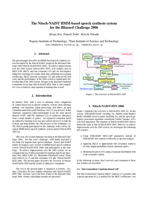
2. Introduction
In January 2005, with a view to allowing closer comparison of corpus-based text-to-speech synthesis systems from labeling, pruning, cost functions, signal processing, and others, an open evaluation named Blizzard Challenge 2005 [1] was devised. In this challenge, organizers asked participants to use the same speech datasets (CMU ARCTIC databases [2]) to synthesize utterances from a small number of genres. An organized evaluation based on subjective listening tests was also carried out to try to rank the systems and help identify the effectiveness of the techniques [3]. The Nitech group participated in this challenge with a newly designed HMM-based speech synthesis system named Nitech-HTS 2005 [4]. This year, the second challenge was held as the Blizzard Challenge 2006. For this year’s challenge, ATR kindly provided a five-hour US English male speech database. Nitech and NAIST jointly developed a new version of HMM-based speech synthesis system (Nitech-NAIST-HTS 2006) and participated in the challenge. To achieve improvements over the 2005 system, we investigated the use of Mel-Generalized Cepstrum-based Line Spectrum Pair (MGC-LSP) [5], Maximum Likelihood Linear Transform (MLLT) [6, 7], and full covariance GV pdf. Nitech-NAISTHTS 2006. The present paper describes the overview of NitechNAIST-HTS 2006 and the results of subjective evaluations. The rest of the present paper is organized as follows. Section 2 describes the new features integrated into Nitech-NAISTHTS 2006. Section 3 gives the brief results of the Blizzard Challenge 2006. Finally concluding remarks are presented.
双频激电及其数据处理

甘肃某金银矿点 金银矿受断裂带产于绿泥石角闪片岩、绢云母石英片岩内的挤压带中,金、银与铅、锌、黄铁矿化共生,且有正相关关系。黄铁矿化较强处可呈稠密浸染至半块状。图为该矿体IV号剖面综合图。Fs 与 ηs 相似性也是一目了然。
时间域与频率域的差异
频率域电法的主要优点 a.轻便; b.抗干扰能力强。 传统频率域电法的主要缺点 任何一种频率域电法都是要在不同的频率进行测量,传统的主动源电法勘探(包括激发极化法和电磁法)的工作方式都是“变频法”,变频法是一个频率、一个频率地逐个改变频率进行测量,以致带来了它两大致命弱点. a.变频法的工作效率低(“扫面”的速度更低); b.变频法的相对精度低。 (1)在激电法中区分矿异常性质能力低, (2)在电磁法(CSAMT)中发现深部异常能力低。 (3)不能(像TEM那样)进行近区的频率域电磁测深。
电流脉冲宽度 T(即充电时间长度) 对极化强度的影响
ΔV0
电位差ΔV
ΔV0
时间 (t)
T大,二次电位大
电位差ΔV
ΔV0
ΔV0
T小,二次电位小
T
T
二次电位差 ΔVIP
频率域与时间域的等效性
脉冲宽度 (T)
电位差 ΔV
二次电位差 ΔVIP
ΔVIP
时间域
时间域
频率域
二次电位差 ΔVIP
频率域IP与时间域IP的物理实质是一样的,对于寻找金属矿来说它们的能力是等效的。
01
对于线性时不变系统,在理论上二者是可以相互转换的。
02
在实际条件下,一般电流密度都非常小(小于0.01μA/cm2),实际上可以看作线性系统,如果能测量到相当完整的时间响应和频率响应,则它们在一定精度内也是可以相互转换的。
Agilent NFA系列噪声分析器配置指南说明书

AgilentN8972A, N8973A, N8974A, N8975A NFA Series Noise Figure AnalyzersConfiguration GuideThis configuration guide will assist withoptimization of an NFA series noise figureanalyzer for specific applications.Models• N8972A noise figure analyzer (10 MHz to 1.5 GHz)• N8973A noise figure analyzer (10 MHz to 3.0 GHz)• N8974A noise figure analyzer (10 MHz to 6.7 GHz)• N8975A noise figure analyzer (10 MHz to 26.5 GHz) 1981NFA series noise figure analyzersN8972A 10 MHz to 1.5 GHz NFA series noise figure analyzerN8973A 10 MHz to 3.0 GHz NFA series noise figure analyzerN8974A 10 MHz to 6.7 GHz NFA series noise figure analyzerN8975A 10 MHz to 26.5 GHz NFA series noise figure analyzerStandard NFA seriesnoise figure analyzers include:• A flexible and intuitive user interface•Easy measurement setup•Low instrument uncertainty•Color graphical display of noise figure and gain versus frequency•Enhanced PC and printer connectivity•SNS series noise source compatible•Ability to automatically upload ENR calibrationdata from SNS series noise sources•Local oscillator control through second dedicated GPIB•3-year warranty as standardUpgrading a modelAll options other than those marked with *, can be ordered at any time for use with an instrument.Noise sources(required to make noise figure measurements)The Agilent SNS Series of noise sources are recommended for use with the Agilent NFA. These noise sources work in conjunction with the NFA Series analyzers to simplify measurement set-up and improve accuracy.Frequency range:N4000A nominal ENR 6dB 10MHz to 18GHzN4001A nominal ENR 15dB 10MHz to 18GHzN4002A nominal ENR 15dB 10MHz to 26.5GHzThe new SNS Series of noise sources are designed specifically for use with the NFA Series of noise figure analyzers. The new noise sources cover the majority of applications with a range of frequencies, ENR and also coaxial connector types.Unique calibration data is stored electronically inside the SNS and is automatically downloaded when connectedto the Agilent noise figure analyzer. The SNS Series also has the capability to measure it’s own temperature so that compensation can be applied to it’s calibration. These features will lead to more reliable measurements.Other compatible noise sources include the Agilent 346 (co-axial) series and the 347 (waveguide) series. Compatible local oscillatorsThe NFA Series noise figure analyzers support the use ofa local oscillator as part of your measurement setup, if you are making measurements on frequency translating devices or making measurements our of one standard frequency range of your noise figure analyzer. SCPI compatible signal generators are recommended, but users may also use their own custom command set.Please note: Care must be taken when specifying a local oscillator, as factors such as phase noise, spectral purity and noise floor of the signal generator may affect noise figure measurements. Filtering may therefore be required on some models of signal generators to enable accurate noise figure measurements to be made. Compatible printersA supported printer is defined as one that is equipped with a parallel interface and accepts printer control language (PCL) level 3 or 5. Purchase an IEEE 1284 compliant printer cable to enable the printer to be used.For further informationAgilent NFA Series – noise figure analyzer applicationand product information is listed below.Key literaturePlease visit the Agilent noise figure analysis web site for on-line access to literature or contact your local Agilent sales office or representative.NFA Series - Noise Figure Analyzers, Brochure,literature number 5980-0166ENFA Series - Noise Figure Analyzers,Technical Specifications, literature number 5980-0164E NFA Series – Noise Figure AnalyzerProgramming Examples,literature number 5968-9498E Fundamental of RF and Microwave Noise Figure Measurements, Application Note 57-1,literature number 5952-8255ENoise Figure Measurement Accuracy ApplicationNote 57–2, literature number 5968-4545E10 Hints for Making Successful Noise Figure Measurements, Application Note 57-3,literature number 5980-0288ESNS Series – Noise Sources, Product Overview,literature number 5988-0081ENKey web resourcesFor the latest information on our noise figure solutions, visit our web page at:/find/nfFor the latest news on the component test industry,visit our web page at:/find/component_testFor on-line manuals, visit our web page at:/find/manualsFundamentals of Noise Figure Measurements Net Seminar (archived version)3Agilent Technologies’ Test and Measurement Support, Services, and AssistanceAgilent Technologies aims to maximize the value you receive, while mini-mizing your risk and problems. We strive to ensure that you get the test and measurement capabilities you paid for and obtain the support you need. Our extensive support resources and services can help you choose the right Agilent products for your applications and apply them success-fully. Every instrument and system we sell has a global warranty. Support is available for at least five years beyond the production life of the prod-uct. Two concepts underlie Agilent’s overall support policy: “Our promise” and “Your Advantage.”Our PromiseOur Promise means your Agilent test and measurement equipment will meet its advertised performance and functionality. When you are choos-ing new equipment, we will help you with product information, including realistic performance specifications and practical recommendations from experienced test engineers. When you use Agilent equipment, we can verify that it works properly, help with product operation, and provide basic measurement assistance for the use of specified capabilities, at no extra cost upon request. Many self-help tools are available.Your AdvantageYour Advantage means that Agilent offers a wide range of additional expert test and measurement services, which you can purchase accord-ing to your unique technical and business needs. Solve problems effi-ciently and gain a competitive edge by contracting with us for calibration,extra-cost upgrades, out-of-warranty repairs, and on-site education and training, as well as design, system integration, project management, and other professional engineering services. Experienced Agilent engineers and technicians worldwide can help you maximize your productivity, opti-mize the return on investment of your Agilent instruments and systems,and obtain dependable measurement accuracy for the life of those products.Get the latest information on the products and applications you select.By internet, phone, or fax, get assistance with all your test & measurement needsOnline assistance:/find/assistPhone or Fax Product specifications and descriptions in this document subject to change without notice.© Agilent Technologies, Inc. 2002Printed in USA, June 5, 20025980-0163EUnited States:(tel) 800 452 4844Canada:(tel) 877 894 4414(fax) 905 282 6495China:(tel) 800 810 0189(fax) 800 820 2816Europe:(tel) (31 20) 547 2323(fax) (31 20) 547 2390Japan:(tel) (81) 426 56 7832(fax) (81) 426 56 7840Korea:(tel) (82 2) 2004 5004 (fax) (82 2) 2004 5115Latin America:(tel) (305) 269 7500(fax) (305) 269 7599Taiwan:(tel) 0800 047 866 (fax) 0800 286 331Other Asia Pacific Countries:(tel) (65) 6375 8100 (fax) (65) 6836 0252Email:*******************/find/emailupdatesGet the latest information on the products and applications you select.Agilent Email Updates。
【图像分析与计算机视觉-英文版】精品讲义-Lec3 Image Enhancement in the Spatial Domain I
Image Analysis and Computer Vision
September 16, 2010 10 / 51
Piecewise-Linear Transformation Functions Case 2:Gray-level Slicing
W.Q. Wang (SISE,GUCAS)
W.Q. Wang (SISE,GUCAS)
Image Analysis and Computer Vision
September 16, 2010 3 / 51
Outline
1 Background 2 Intensity Transformation Functions 3 Image Histogram Processing
W.Q. Wang (SISE,GUCAS)
Image Analysis and Computer Vision
September 16, 2010 8 / 51
Power-Law Transform Example 3: Contrast manipulation
W.Q. Wang (SISE,GUCAS)
g(x, y) = T [f (x, y)]
where f (x, y): the input image g(x, y): the processed image T : an operator on f , defined over some neighborhood of (x, y)
T can operate on a set of images, e.g., noise reduction Square and rectangular neighborhood are by far the most popular due to their ease of implementation, although circle is also used.
IEC61967-3_Surface_Scan
2004-07-09
IEC CISPR/A
Functions concerned Safety EMC
47A/674/CD - 47A/685A/CC
Environment Quality assurance
THIS DOCUMENT IS STILL UNDER STUDY AND SUBJECT TO CHANGE. IT SHOULD NOT BE USED FOR REFERENCE PURPOSES. RECIPIENTS OF THIS DOCUMENT ARE INVITED TO SUBMIT, W ITH THEIR COMMENTS, NOTIFICATION OF ANY RELEVANT PATENT RIGHTS OF WHICH THEY ARE AW ARE AND TO PROVIDE SUPPORTING DOCUMENTATION.
FORM DTS (IEC) 2002-08-09
61967-3 Ed.1/ DTS IEC
2
TABLE OF CONTENTS
FOREWORD........................................................................................................................... 4 1 2 3 4 5 Scope............................................................................................................................... 6 Normative References ...................................................................................................... 6 Definitions ........................................................................................................................ 6 General ............................................................................................................................ 7 Test Conditions ................................................................................................................7 5.1 Supply voltage ........................................................................................................ 7 5.2 Frequency range ..................................................................................................... 7 Test Equipment ................................................................................................................ 8 6.1 6.2 6.3 6.4 Shielding ................................................................................................................. 8 RF measuring instrument ........................................................................................ 8 Preamplifier............................................................................................................. 8 Near field probe ...................................................................................................... 8 6.4.1 Magnetic (H) field probe .............................................................................. 8 6.4.2 Electric (E) field probe ................................................................................. 9 6.4.3 Electromagnetic (E/H) field probe ................................................................ 9 6.5 Probe positioning and data acquisition system ........................................................ 9 Test Set-up ...................................................................................................................... 9 7.1 7.2 7.3 Test 8.1 8.2 8.3 Test 9.1 9.2 9.3 Test configuration.................................................................................................... 9 Test PCB............................................................................................................... 11 Scan software set-up............................................................................................. 11 Procedure ............................................................................................................... 11 Ambient conditions ................................................................................................ 11 Operational check ................................................................................................. 11 Test technique ...................................................................................................... 11 Report .................................................................................................................... 12 Measurement conditions........................................................................................ 12 Probe design and calibration ................................................................................. 12 Data analysis ........................................................................................................ 12
量子频率标准Quantum Frequency Standards Chapter6

6.1 Storage of Atoms and Molecules in a Cell
The confinement of absorbers in a suitable container for interrogation has a number of distinct advantages. Besides allowing for a compact set-up, the absorbing material can be prepared and kept at well defined conditions, e.g., at constant temperature or pressure. It furthermore allows one to make economic use of expensive material with defined purity or isotopic composition.
Hence, the progress achieved in the past with frequency standards was intimately related to the development of novelmethods for interrogating and manipulating the absorbers under well defined conditions.
6.5 Doppler-free Non-linear Spectroscopy
6.5.1 Saturation Spectroscopy 6.5.2 Power-dependent Selection of Low-velocity Absorbers 6.5.3 Two-photon Spectroscopy
6EQ资料
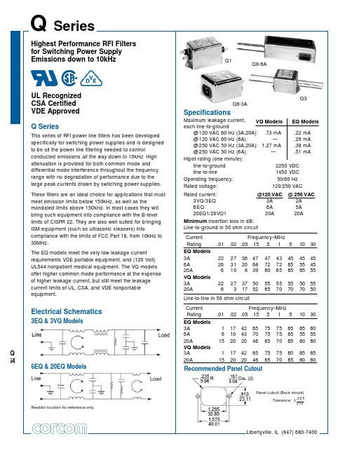
.0 0 5
0.13
Libertyville, IL (847) 680-7400
元器件交易网
Series
Case Styles
Metric shown in italics.
Q
Case Style
Metric shown in italics.
Q1
6A-Q8 & Q8M
Line-to-line in 50 ohm circuit Current Rating EQ Models 3A 6A 20A VQ Models 3A 20A .01 1 6 15 1 15 Frequency–MHz .02 .05 .15 .5 1 5 17 10 20 17 20 42 43 20 42 20 65 70 46 65 46 75 75 65 75 65 75 75 70 75 70 65 65 65 60 65 10 30 65 60 55 55 60 60 65 65 60 60
Electrical Schematics
3EQ & 3VQ Models
Q 64 6EQ & 20EQ Models
Recommended Panel Cutout
Panel cutout (Back mount) Tolerance: ± Resistor location for reference only.
(5) Holes:
.0 7
1.8
Dia.(4) Slot:
.07 x .16
1.8 x 4.1
Mounting holes:
.188
4.78
Dia.(2)
3VQ3, 3EQ3 3VQ8, 3VQ8M 3EQ8, 3EQ8M 6EQ1 6EQ3 6EQ8, 6EQ8M 20EQ1,20VQ1
LM3687 Evaluation Board User's Guide
User's GuideSNVA249A–July2008–Revised April2013AN-1647LM3687Evaluation Board1IntroductionThis evaluation board is designed to enable independent evaluation of the LM3687electrical performance.Each board is pre-assembled and tested in the factory.The evaluation kit is available in two options:LM3687TL-1812EV and LM3687TL-1815EV.For othervoltage options,the device can be ordered from LM3687product folder on the TI website.The board contains the LM3687,an inductor,and input and output capacitors connected to GND.This user's guide contains information about the evaluation board.For further information on deviceelectrical characteristics and component selection,please refer to LM3687Step-Down DC-DC Converter with Integrated Low Dropout Regulator and Startup Mode(SNVS473).2General DescriptionThe LM3687is a high efficiency synchronous switching step-down DC-DC converter with an integrated low dropout Linear Regulator optimized for powering ultra-low voltage circuits from a single Li-Ion cell or3 cell NiMH/NiCd batteries.It provides a dual output with fixed output voltages and combined load current up to750mA in post regulation mode or1100mA in independent mode of operation.The LM3687is capable of operating with input voltage ranges from2.7V≤VBATT ≤5.5V and0.7V≤VIN_LIN≤4.5V.It also features internal protection against short-circuit and over-temperature conditions.For the Evaluation Board the typical post regulation application is realized:the output voltage of the DC-DC converter is used as supply for the linear regulator(VOUT_DCDC =VIN_LIN).Thereby a higher efficiency andlower power dissipation of the system can be achieved compared to using the battery voltage VBATT assupply for the linear regulator(VIN_LIN).For both available evaluation kit options the output voltage of the DC-DC converter is1.8V and therefore sufficiently high as supply for both linear regulator output voltage options(the power input voltage appliedat VIN_LIN should be at least0.25V above the nominal output voltage of the linear regulator).VBATTshouldbe at least1.5V above the output voltage of the linear regulator(VOUT_LIN )and1.0V above the outputvoltage of the DC-DC converter(VOUT_DCDC )(with a minimum of2.7V)to operate the device withinoperating conditions.That means for the1.8V-1.2V combination,the minimum VBATT =2.8V and for the1.8V-1.5V combination it is3.0V.Input connections should be kept reasonably short(<20cm)to minimize input inductance and ensure optimum transient performance.It's good practice to twist the wires to the supply for minimum inductance. ON/OFF control of the LM3687outputs is provided on the evaluation board by a logic signal applied to theenable pins VEN_DCDC and VEN_LIN.To simplify the enabling of the outputs,two'three pin jumpers'areprovided on the board:•J5to enable the DC-DC converter•J6to enable the linear regulatorThe middle pins of the two jumpers are directly connected to the appropriate enable pins of the device.A logic signal with a minimum of1.0V to enable the output or with a maximum of0.4V to disable it can be directly connected to this jumper pin in the middle.Alternatively the middle pin can be shorted to the pin next to it to the left(marked ON,shorted to VBATT)or to the right.All trademarks are the property of their respective owners.1 SNVA249A–July2008–Revised April2013AN-1647LM3687Evaluation Board Submit Documentation FeedbackCopyright©2008–2013,Texas Instruments IncorporatedVOUT_DCDCGNDVBATTVOUT_LINGNDVIN_LINJP1Schematic Diagram A load of up to 750mA maximum may be connected from the V OUT_DCDC pin to GND if no additional load is applied at the output of the linear regulator.For V OUT_LIN ,the maximum load is 350mA.As in the typical post regulation application the load of the linear regulator is supplied by the DC-DC converter,the combined maximum load conditions are:350mA at V OUT_LIN plus 400mA at V OUT_DCDC .At the top of the board the output voltage option (1812or 1815)is printed.The 'connectors'J1,J2,J3,and J4represents a 'sense path'to V OUT_DCDC ,V IN_LIN ,V BATT and V OUT_LIN .They can be used for more precise voltage measurements or to connect a differential probe.In case the two regulators shall be operated independently instead of in the post regulation mode,the connection from V OUT_DCDC to V IN_LIN can be removed by cutting the trace between the two pads at JP1.Then an external source needs to be connected to V IN_LIN .V BATT is still needed for the linear regulator as well,it supplies internal circuitry.It's important that V IN_LIN does not exceed V BATT at any time .An input capacitor of 1.0µF at V IN_LIN needs to be added if no other filter bypass capacitor is present in this supply path.3Schematic DiagramFigure 1.Evaluation Board Schematic2AN-1647LM3687Evaluation BoardSNVA249A–July 2008–Revised April 2013Submit Documentation FeedbackCopyright ©2008–2013,Texas Instruments Incorporated Evaluation Board Top Layer Layout 4Evaluation Board Top Layer LayoutFigure2.Top Layer Board LayoutBoard Size:40mm×45mm3 SNVA249A–July2008–Revised April2013AN-1647LM3687Evaluation Board Submit Documentation FeedbackCopyright©2008–2013,Texas Instruments IncorporatedSGNDB2V OUT_LINV IN_LIN EN_LINEN_DCDCPGND V BATTSW FB_DCDCA1 B1 C1 C2 A3B3C3A2Evaluation Board Picture Top Side 5Evaluation Board Picture Top SideFigure 3.Picture Top Side6Connection DiagramFigure 4.Connection Diagram 9-Bump Thin DSBGA Package,Large Bump,0.5mm Pitch4AN-1647LM3687Evaluation BoardSNVA249A–July 2008–Revised April 2013Submit Documentation FeedbackCopyright ©2008–2013,Texas Instruments Incorporated Bill of MaterialsTable1.Pin DescriptionsPin#Name DescriptionA1PGND Power Ground pinA2SGND Signal Ground pinA3V OUT_LIN Voltage Output of the linear regulatorB1SW Switching Node Connection to the internal PFET switch and NFET synchronous rectifierB2EN_DCDC Enable Input for the DC-DC converter.The DC-DC converter is in shutdown mode if voltage atthis pin is<0.4V and enabled if>1.0V.Do not leave this pin floating.See Table2.B3V IN_LIN Power Supply Input for the linear regulatorC1V BATT Power Supply for the DC-DC output stage and internal circuitry.Connected to the input filtercapacitor.C2FB_DCDC Feedback Analog Input for the DC-DC converter.Directly connected to the output filter capacitor.C3EN_LIN Enable Input for the linear regulator.The linear regulator is in shutdown mode if voltage at this pinis<0.4V and enabled if>1.0V.Do not leave this pin floating.See Table2.Table2.Enable CombinationsEN_DCDC EN_LIN Comments00No Outputs01Linear Regulator enabled only(1)10DC-DC converter enabled only11DC-DC converter and linear regulator active(1)(1)Startup Mode:•V IN_LIN must be higher than V OUT_LIN(NOM)+200mV in order to enable the main regulator(I MAX=350mA).•If V IN_LIN<V OUT_LIN(NOM)+100mV(100mV hysteresis),the startup LDO(I MAX=50mA)is active,supplied from V BATT.For example in the typical post regulation application,the LDO will remain in startup mode until the DC-DC converter hasramped up its output voltage.7Bill of MaterialsTable3.Bill of MaterialsItem Description Qty Footprint Mfg.,Part NumberC1C IN_LIN,ceramic capacitor,1µF,X5R at V IN_LIN,00603/0402optional,not needed in post regulationapplication due to C4C2C BATT,ceramic capacitor,4.7µF,X5R at V BATT10805/0603TDK,C1608X5R1A475KC3C OUT_LIN,ceramic capacitor,2.2µF,X5R at10603/0402TDK,C1608X5R1A225K V OUT_LINC4C OUT_DCDC,ceramic capacitor,10µF,X5R at10805/0603TDK,C1608X5R0J106K V OUT_DCDCL1Inductor,2.2µH,1.6A I SAT1Coilcraft,DO3314-222MLB U1LM368719-bump DSBGA Texas Instruments,YZR0009BBA LM3687 V BATT,V OUT_DCDC,Terminal5Cambion,160-1026-02-05 V OUT_LIN,2x GNDJ5,J63pin jumper for enable function25 SNVA249A–July2008–Revised April2013AN-1647LM3687Evaluation Board Submit Documentation FeedbackCopyright©2008–2013,Texas Instruments IncorporatedApplication Hints 8Application Hints8.1Power Dissipation and Device OperationThe permissible power dissipation for any package is a measure of the capability of the device to pass heat from the power source,the junctions of the IC,to the ultimate heat sink,the ambient environment.Thus the power dissipation is dependent on the ambient temperature and the thermal resistance across the various interfaces between the die and ambient air.The allowable power dissipation for the device in a given package can be calculated using the following equation:PD_SYS =(TJ(MAX)-TA)/θJA(1)For the LM3687there are two different main sources contributing to the systems power dissipation(PD_SYS):•the DC-DCconverter(PD_DCDC)•the linear regulator(PD_LIN)Neglecting switching losses and quiescent currents these two main contributors can be estimated by the following equations:PD_LIN =(VIN_LIN-VOUT_LIN)×IOUT_LIN(2)PD_DCDC =IOUT_DCDC2×[(RDSON(P)×D)+(RDSON(N)×(1-D))](3)with duty cycle D=VOUT_DCDC /VBATT.As an example,assuming the typical post regulation application,the conversion from VBATT =3.6V toVOUT_DCDC =1.8Vand further to VOUT_LIN=1.5V,at maximum load currents,results in following powerdissipations:PD_DCDC=(0.75A)2×(0.38Ω×1.8V/3.6V+0.25Ω×(1-1.8V/3.6V))=177mW andPD_LIN=(1.8V-1.5V)×0.35A=105mWPD_SYS=282mWWith aθJA =70°C/W for the DSBGA9package,this PD_SYSwill cause a rise of the junction temperature TJof:ΔTJ =PD_SYS×θJA=20KFor the same conditions but the linear regulator biased from VBATT ,this results in a PD_LINof735mW,PD_DCDC =50mW(because IOUT_DCDC=400mA)and therefore an increase of TJ=55K.As lower total powerdissipation translates to higher efficiency this example highlights the advantage of the post regulationsetup.6AN-1647LM3687Evaluation Board SNVA249A–July2008–Revised April2013Submit Documentation FeedbackCopyright©2008–2013,Texas Instruments IncorporatedIMPORTANT NOTICETexas Instruments Incorporated and its subsidiaries(TI)reserve the right to make corrections,enhancements,improvements and other changes to its semiconductor products and services per JESD46,latest issue,and to discontinue any product or service per JESD48,latest issue.Buyers should obtain the latest relevant information before placing orders and should verify that such information is current and complete.All semiconductor products(also referred to herein as“components”)are sold subject to TI’s terms and conditions of sale supplied at the time of order acknowledgment.TI warrants performance of its components to the specifications applicable at the time of sale,in accordance with the warranty in TI’s terms and conditions of sale of semiconductor products.Testing and other quality control techniques are used to the extent TI deems necessary to support this warranty.Except where mandated by applicable law,testing of all parameters of each component is not necessarily performed.TI assumes no liability for applications assistance or the design of Buyers’products.Buyers are responsible for their products and applications using TI components.To minimize the risks associated with Buyers’products and applications,Buyers should provide adequate design and operating safeguards.TI does not warrant or represent that any license,either express or implied,is granted under any patent right,copyright,mask work right,or other intellectual property right relating to any combination,machine,or process in which TI components or services are rmation published by TI regarding third-party products or services does not constitute a license to use such products or services or a warranty or endorsement e of such information may require a license from a third party under the patents or other intellectual property of the third party,or a license from TI under the patents or other intellectual property of TI.Reproduction of significant portions of TI information in TI data books or data sheets is permissible only if reproduction is without alteration and is accompanied by all associated warranties,conditions,limitations,and notices.TI is not responsible or liable for such altered rmation of third parties may be subject to additional restrictions.Resale of TI components or services with statements different from or beyond the parameters stated by TI for that component or service voids all express and any implied warranties for the associated TI component or service and is an unfair and deceptive business practice. TI is not responsible or liable for any such statements.Buyer acknowledges and agrees that it is solely responsible for compliance with all legal,regulatory and safety-related requirements concerning its products,and any use of TI components in its applications,notwithstanding any applications-related information or support that may be provided by TI.Buyer represents and agrees that it has all the necessary expertise to create and implement safeguards which anticipate dangerous consequences of failures,monitor failures and their consequences,lessen the likelihood of failures that might cause harm and take appropriate remedial actions.Buyer will fully indemnify TI and its representatives against any damages arising out of the use of any TI components in safety-critical applications.In some cases,TI components may be promoted specifically to facilitate safety-related applications.With such components,TI’s goal is to help enable customers to design and create their own end-product solutions that meet applicable functional safety standards and requirements.Nonetheless,such components are subject to these terms.No TI components are authorized for use in FDA Class III(or similar life-critical medical equipment)unless authorized officers of the parties have executed a special agreement specifically governing such use.Only those TI components which TI has specifically designated as military grade or“enhanced plastic”are designed and intended for use in military/aerospace applications or environments.Buyer acknowledges and agrees that any military or aerospace use of TI components which have not been so designated is solely at the Buyer's risk,and that Buyer is solely responsible for compliance with all legal and regulatory requirements in connection with such use.TI has specifically designated certain components as meeting ISO/TS16949requirements,mainly for automotive use.In any case of use of non-designated products,TI will not be responsible for any failure to meet ISO/TS16949.Products ApplicationsAudio /audio Automotive and Transportation /automotiveAmplifiers Communications and Telecom /communicationsData Converters Computers and Peripherals /computersDLP®Products Consumer Electronics /consumer-appsDSP Energy and Lighting /energyClocks and Timers /clocks Industrial /industrialInterface Medical /medicalLogic Security /securityPower Mgmt Space,Avionics and Defense /space-avionics-defense Microcontrollers Video and Imaging /videoRFID OMAP Applications Processors /omap TI E2E Community Wireless Connectivity /wirelessconnectivityMailing Address:Texas Instruments,Post Office Box655303,Dallas,Texas75265Copyright©2013,Texas Instruments Incorporated。
- 1、下载文档前请自行甄别文档内容的完整性,平台不提供额外的编辑、内容补充、找答案等附加服务。
- 2、"仅部分预览"的文档,不可在线预览部分如存在完整性等问题,可反馈申请退款(可完整预览的文档不适用该条件!)。
- 3、如文档侵犯您的权益,请联系客服反馈,我们会尽快为您处理(人工客服工作时间:9:00-18:30)。
The two-dimensional Fourier transform and its inverse
10 / 48
2-D Discrete Fourier Transform
Properties of 2-D DFT (cont.)
Seperability F (u, v) = [f (x, y)] = Σy [Σx f (x, y)exp(−j2π xu )]exp(−j2π yv ) M N = Σy F (u, y)exp(−j2π yv ) N The 2D DFT F (u, v) can be obtained by
September 30, 2010
11 / 48
2-D Discrete Fourier Transform
I(u,v) tan−1 [ R(u,v) ]
1
(spectrum)
(phase angle) (powerspectrum)
P (u, v) = |F (u, v)|2 = R2 (u, v) + I 2 (u, v)
I(u, v): the imaginary part of F (u, v). R(u, v): the real part of F (u, v).
−
N 2)
N −1 y=0 f (x, y)
(average)
(conjugate symmetric)
|F (u, v)| = |F (−u, −v)| (symmetric)
W.Q. Wang (SISE,GUCAS)
Image Analysis and Computer Vision
September 30, 2010
Image Analysis and Computer Vision Lecture 6,7!Image Enhencement in Frequency Domain
Weiqiang Wang School of Information Science and Engineering, GUCAS September 30, 2010
1 2
Taking the 1D DFT of every row of image f (x, y), F (u, y). The 1D DFT of every column of F (u, y).
W.Q. Wang (SISE,GUCAS)
Image Analysis and Computer Vision
Fourier transform 1 F (u) = M
M −1 x=0
f (x)e−
j2πux M
f or u = 0, 1, 2, ..., M − 1
Inverse Fourier transform: j2πux M −1 f (x) = u=0 F (u)e M
1 M M −1 2πux x=0 f (x)[cos M
I(u) φ(u) = tan−1 [ R(u) ] (phase angle or phase spectrum)
1
I(u): the imaginary part of F (u). R(u): the real part of F (u).
Power spectrum: P (u) = |F (u)|2 = R2 (u) + I 2 (u)
W.Q. Wang (SISE,GUCAS)
Image Analysis and Computer Vision
September 30, 2010
9 / 48
2-D Discrete Fourier Transform
Properties of 2-D DFT
Time-shifting [f (x − x0 , y − y0 )] = F (u, v)e−j2π( Frequency shifting [f (x, y)e−j2π(
f or x = 0, 1, 2, ..., M − 1
Since ejθ = cos θ + j sin θ, then DCT can be redefined as F (u) = − j sin 2πux ] M f or u = 0, 1, 2, ..., M − 1
Frequency (time) domain: the domain (values of u) over which the values of F (u) range; because u determines the frequency of the components of the transform. Frequency (time) component: each of the M terms of F (u).
W.Q. Wang (SISE,GUCAS)
Image Analysis and Computer Vision
September 30, 2010
8 / 48
2-D Discrete Fourier Transform
2-D Discrete Fourier Transform
We define the Fourier spectrum, phase angle, and power spectrum as follows: |F (u, v)|2 = [R2 (u, v) + I 2 (u, v)] 2 φ(u, v) =
W.Q. Wang (SISE,GUCAS) Image Analysis and Computer Vision September 30, 2010 3 / 48
2-D Discrete Fourier Transform
2-D Continuous Fourier Transform
The one-dimensional Fourier transform and its inverse
M −1 u=0 N −1 v=0
F (u, v)ej2π( M + N )
ux
vy
f or x = 0, 1, 2, ..., M − 1, y = 0, 1, 2, ..., N − 1
u,v: the transform or frequency variables x,y: the spatial or image variables
W.Q. Wang (SISE,GUCAS)
Image Analysis and Computer Vision
September 30, 2010
1 / 48
Outline
1
2-D Discrete Fourier Transform Filtering in the Frequency Domain Obtaining Frequency Domain Filters from Spatial Filters Generating Filters Directly in the Frequency Domain Sharpening Frequency Domain Filters
2
3
4
5
W.Q. Wang (SISE,GUCAS)
Image Analysis and Computer Vision
September 30, 2010
2 / 48
2-D Discrete Fourier Transform
2-D Fourier Transform
Any function that periodically repeats itself can be expressed as the sum of sines and/or cosines of different frequencies, each multiplied by a different coefficient (Fourier series). Even functions that are not periodic (but whose area under the curve is finite) can be expressed as the integral of sines and/or cosines multiplied by a weighting function (Fourier transform). The frequency domain refers to the plane of the two dimensional discrete Fourier transform of an image. The purpose of the Fourier transform is to represent a signal as a linear combination of sinusoidal signals of various frequencies.
Fourier transform ∞ F (u) = −∞
∞ −∞
f (x, y)e−j2π(ux+vy) dxdy
Inverse Fourier transform: ∞ ∞ f (x, y) = −∞ −∞ F (u, v)ej2π(ux+vy) dudv
W.Q. Wang (SISE,GUCAS)
Image Analysis and Computer Vision
September 30, 2010
7 / 48
2-D Discrete Fourier Transform