RJZ-2405SHP中文资料
电气控制柜LED照明系统
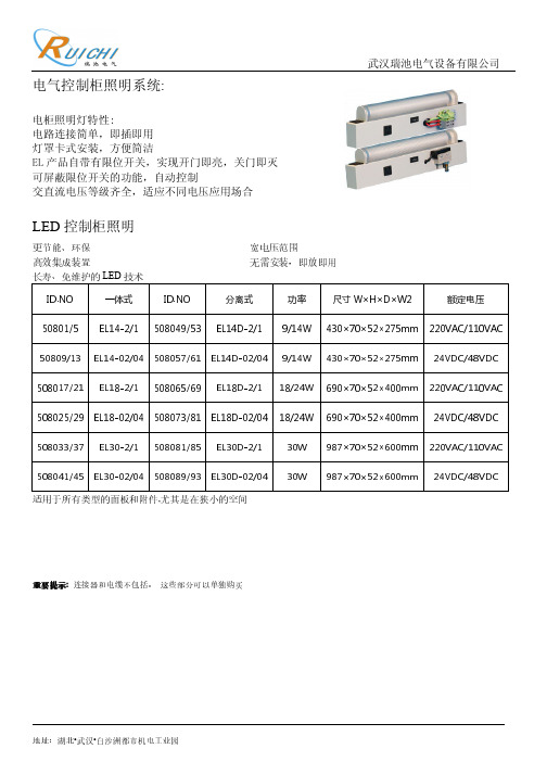
武汉瑞池电气设备有限公司地址:湖北•武汉•白沙洲都市机电工业园电气控制柜照明系统:电柜照明灯特性:电路连接简单,即插即用灯罩卡式安装,方便简洁EL 产品自带有限位开关,实现开门即亮,关门即灭可屏蔽限位开关的功能,自动控制交直流电压等级齐全,适应不同电压应用场合LED 控制柜照明更节能、环保 宽电压范围高效集成装置 无需安装,即放即用 长寿、免维护的LED 技术ID.NO一体式 ID.NO 分离式 功率 尺寸W×H×D×W2 额定电压 50801/5EL14-2/1 508049/53 EL14D-2/1 9/14W 430×70×52×275mm 220VAC/110VAC 50809/13EL14-02/04 508057/61 EL14D-02/04 9/14W 430×70×52×275mm 24VDC/48VDC 508017/21 EL18-2/1 508065/69 EL18D-2/1 18/24W 690×70×52×400mm 220VAC/110VAC508025/29 EL18-02/04 508073/81 EL18D-02/04 18/24W690×70×52×400mm 24VDC/48VDC 508033/37 EL30-2/1 508081/85 EL30D-2/1 30W987×70×52×600mm 220VAC/110VAC 508041/45 EL30-02/04 508089/93 EL30D-02/0430W 987×70×52×600mm 24VDC/48VDC 适用于所有类型的面板和附件,尤其是在狭小的空间重要提示: 连接器和电缆不包括。
这些部分可以单独购买。
RN-2405SHP中文资料
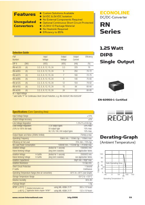
Features
Unregulated Converters
● ● ● ● ● ● ●
Custom Solutions Available 1kVDC & 2kVDC Isolation No External Components Required Optional Continuous Short Circuit Protected UL94V-0 Package Material No Heatsink Required Efficiency to 85%
Deviation from Nominal (%)
15.000 10.000 5.000 0.000 -5.000 -10.000
Deviation from Nominal (%)
0505
15.000 10.000 5.000 0.000 -5.000 -10.000
0509
1205
1209
0% 20% 40% 60% Total Output current (%)
ECONOLINE
DC/DC-Converter
RN Series
1.25 Watt DIP8 Single Output
Selection Guide
Part Number DIP 8 RN-xx3.3S RN-xx05S RN-xx07S RN-xx09S RN-xx12S RN-xx15S (2kV) (H) (H) (H) (H) (H) (H) Input Voltage (VDC) 3.3, 5, 9, 12, 15, 24 3.3, 5, 9, 12, 15, 24 3.3, 5, 9, 12, 15, 24 3.3, 5, 9, 12, 15, 24 3.3, 5, 9, 12, 15, 24 3.3, 5, 9, 12, 15, 24 Output Voltage (VDC) 3.3 5 7 9 12 15 Output Current (mA) 378 250 180 140 104 84 Efficiency (%) 70 70-72 72-75 75-80 79-82 80-84 80-85
2405使用说明书(英文)041122
中央控制器FS2405使用说明书MDS CENTRAL UNIT FS2405InstructionPD10. UMN. FS2405拟制日期审核日期标准化日期批准日期弗曼科斯(上海)电子有限公司文件序列号:PDA13版本号:V1.0中央控制器FS2405使用说明书MDS CENTRAL UNIT FS2405InstructionPD10. UMN. FS24051产品名称NAME、型号model产品名称:中央控制器MDS CENTRAL UNIT,产品型号:FS2405。
2适用范围适用于MDS系统。
The MDS Central Unit can be used in MDS system.3主要功能及技术参数Characteristics And Features3.1 主要功能Characteristics3.1.1负责管理MDS Digital系统,其中包括音频视频信号的通断控制、出入口的控制、电梯的控制及其自动化、监控全部连接在中控器上的设备的运行。
The MDS Central Unit can work as an audio door entry system(including video signal)working as an MDS-DIGITAL system and also as an entry access control system, working as an MDS-Digital Controller.3.1.2Electronic directory of users: name, apartment, door number…(up to 1020 registers).存储用户信息:姓名、楼层、房号、开门密码及分组。
(1020位住户)。
3.1.3多个中控器可进行FXL联网(最多可连接63个)。
Central Units FXL networklinkable(up to 63).3.1.4远程PC管理,通过REF. 2466 PC接口可直接连接打印机,即时打印或存储信息。
管状电动机性能
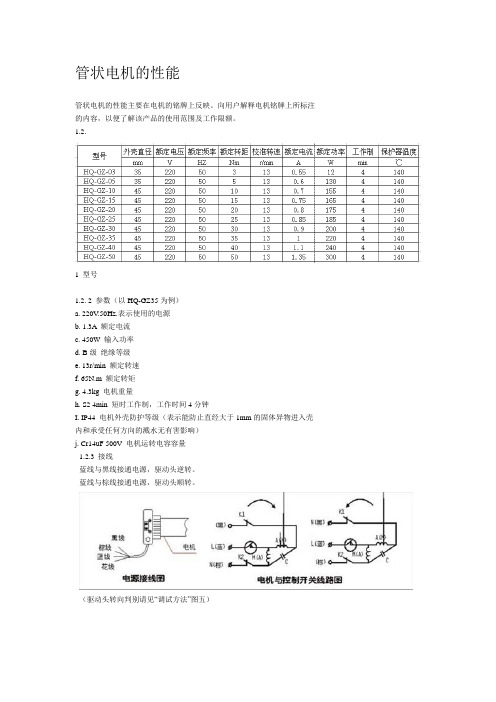
管状电机的性能管状电机的性能主要在电机的铭牌上反映。
向用户解释电机铭牌上所标注的内容,以便了解该产品的使用范围及工作限额。
1.2.1 型号1.2. 2 参数(以HQ-GZ35为例)a. 220V.50Hz.表示使用的电源b. 1.3A 额定电流c. 450W 输入功率d. B级绝缘等级e. 13r/min 额定转速f. 65N.m 额定转矩g. 4.3kg 电机重量h. S2 4min 短时工作制,工作时间4分钟I. IP44 电机外壳防护等级(表示能防止直经大于1mm的固体异物进入壳内和承受任何方向的溅水无有害影响)j. Cr14uF 500V 电机运转电容容量1.2.3 接线蓝线与黑线接通电源,驱动头逆转。
蓝线与棕线接通电源,驱动头顺转。
(驱动头转向判别请见“调试方法”图五)1.2.4.使用寿命与噪音(在额定负载下)a.使用寿命≥7500次(一个单程为一次)b.噪音HQ-GZ20-HQ-GZ65型≤50dBHQ-GZ80-HQ-GZ100型≤60dB管状电机的调试新用户拿到管状电机后不妨先接通电源试一下(本说明书图一型式用户先将附助开关拨杆处在“合”的位置上),当用引出线的蓝线和黑线(或棕线)接通电源后(也可接上遥控接收器,用遥控器或触摸开关控制),驱动头开始逆转(或顺转)。
同时,将传动套顺驱动头转动方向旋转,直至驱动头停止转动。
将传动套倒回、驱动头又开始向原方向旋转,重复前一动作,驱动头停止转动,证实该旋转方向已限定。
然后调换接线,驱动头换向转动。
如在传动套外圆作一标记, 将传动套按上述方法与驱动头同向转动, 直至驱动头停转,传动套所转过的转数,即为当前驱动头在两限位的转数(出厂前已调至5转左右)。
特别告诫用户,当驱动头被限位控制停止转动时,传动套不得按当前的转向继续转动,否则将损坏机件。
用户要调整电机驱动头转数的大小,可按两调节手轮(或行程调节插孔)之间的调节方向指示来进行。
“十”表示增加转数“一”则减少,黑色指示调整逆转转数,红色指示调整顺转转数(见图五)。
YKD2405PE总线型步进驱动器使用手册说明书
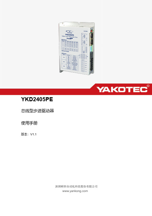
YKD2405PE总线型步进驱动器使用手册版本:V1.1深圳研控自动化科技股份有限公司目录目录 (2)版本修订历史 (1)前言 (2)第1章概述 (3)1.1产品介绍 (3)1.2特性 (3)1.3应用领域 (3)1.4产品命名规则 (4)第2章性能指标 (5)2.1EtherCAT特性 (5)2.2电气特性 (5)2.3使用环境 (6)第3章安装 (7)3.1安装尺寸 (7)3.2安装方法 (7)第4章驱动器端口与接线 (8)4.1接线示意图 (8)4.2端口定义 (9)4.2.1地址拨码 (9)4.2.2状态指示灯 (9)4.2.3EtherCAT通讯端口 (10)4.2.4输入输出端口 (10)4.2.5电机输出端口 (10)4.2.6电源输入端口 (10)4.3输入/输出端口操作 (11)第5章适配电机 (12)5.1电机尺寸 (12)5.2. 技术参数 (13)5.3 电机接线图 (14)第6章驱动器状态指示灯 (15)第7章一般故障排除方法 (16)第8章保修及售后服务 (17)8.1保修 (17)8.2售后服务 (17)YKD2405PE 使用手册 V1.1 版本修订历史版本修订历史YKD2405PE 使用手册 V1.1 前言前言感谢您使用本公司总线型步进驱动器。
在使用本产品前,请务必仔细阅读本手册,了解必要的安全信息、注意事项以及操作方法等。
错误的操作可能引发极其严重的后果。
声明本产品的设计和制造不具备保护人身安全免受机械系统威胁的能力,请用户在机械系统设计和制造过程中考虑安全防护措施,防止因不当的操作或产品异常造成事故。
由于产品的改进,手册内容可能变更,恕不另行通知。
用户对产品的任何改装我公司将不承担任何责任。
阅读时,请注意手册中的以下标示:第1章概述1.1产品介绍YKD2405PE总线型步进伺服驱动器是在数字型步进驱动器的基础上增加了EtherCAT总线通讯功能,同时支持智能运动控制功能。
RU-240505资料
80%
100%
0% 20% 40% 60% Total Output current (%)
80%
100%
Deviation / Load
25.000 20.000 25.000 20.000
Deviation / Load
Deviation from Nominal (%)
Deviation from Nominal (%)
121515
051515
3.31212
0% 20% 40% 60% Total Output current (%) 80% 100%
3.31515
0% 20% 40% 60% Total Output current (%)
80%
100%
April-2005
元器件交易网
Features
Unregulated Converters
● ● ● ● ● ● ● ● ● ●
Twin Independent Outputs Output/Output Isolation 1kVDC Power Sharing on Outputs Input/Output Isolation 1kVDC No Heatsink Required UL94V-0 Package Material Toroidal Magnetics No Extern. Components Required Custom Solutions Available Efficiency to 84%
Input/Output and Output V1/Output V2
46
April-2005
元器件交易网
ECONOLINE
环希工业 240说明书(1)

端子说明:
运行指示 单元指示 数据指示
操作按钮
1# L 2# N 3#TC 4#TA 5#TB 6#GND 7#V4 8#GND 9#V3 10#GND 11#V2 12#GND 13#V1
电电源源220VAC±20%50Hz 输出继电器常开 输出继电器公共端 输出继电器常闭 信号地 单元4输出端[0-10V] 信号地 单元3输出端[0-10V] 信号地 单元2输出端[0-10V] 信号地 单元1输出端[0-10V]
N 1 1A 250V 50Hz
注:电位器建议使用2K-10K
P6-2 江阴市环希工业控制设备有限公司
以上灰色区域为
! 可接强电区,本 机其他端子严禁
接触强电.
参数表
参数号 F01 F02 F03 F04 F05 F06 F07 F08 F09 F10 F11 F12 F13 F14 F15 F16 F17 F18 F19 F20 F21 F22 F23 F24 F25 F26 F27 F28 F29 F30 F31 F32 F33
14#GF1 15#GF2 16#GND 17#+10V 18#GF3 19#GF4 20#GND 21#+10V 22#G1 23#GND 24#UP 25#DOWN 26#RS
反馈1 反馈2 信号地 +10V参考电压,≤50mA 反馈3 反馈4 信号地 同17# 外部主给定1 信号地 上升端子 下降端子 启停端子
0:解锁 ቤተ መጻሕፍቲ ባይዱ:锁定 给定从0升到10V所需时间
范围0-100秒 范围0-13*
! 按ENT则参数恢复出厂值**
范围0.00-10.00
端子26闭合时:0:无动作1:G0=F22 0.01:最慢 4.00:最快
RJ插座产品技术参数

RJ插座产品技术参数电气性能额定电流: 1.5AMPS@25℃额定电压:125V AC绝缘电阻:1000 MΩMin. @ 500V DC耐压强度:1000 V AC RMS,contact to contact 或1500VDC,*************************************或60 Hz 一分钟接触电阻:1XN圆针35 mΩMax.()1XN扁针45 mΩMax.()2XN圆针40 mΩMax.()2XN扁针50 mΩMax.()20 mΩMax. (V )LED灯工作电压:1.8~2.6V;工作电流:20 mA 最大(V )机械性能插入/拔出力:22N / 2.27kg Max. ()30N/3.06KG Max(V)配合强度:封闭型插座50N(V )开口型插座30N Min. ()(V )for 60s±5s使用寿命:750(V )1500()次插拔Min.环境性能工作温度:-40℃~+85℃(V )0℃~+70℃()适用PC / ABS储存温度:-40℃~+85℃(V )0℃~+70℃()适用PC / ABS 相对湿度<80%储存时间:6个月()12个月(V)适用制程:无铅波峰焊260±5℃5~10S(V ); 无铅回流焊265±5℃3-5S();手工焊接:400℃±5℃()360±5℃(V),最大能承受焊接次数3次,每次时间﹤5秒;盐雾测试:镀金规格G/F~1.5 u" ,盐雾测试时间8小时最小(V )镀金规格PDNI15/20 u"、3 u"、6 u",盐雾测试时间24小时最小()镀金规格PD20u"、15 u"、30 u"、50 u",盐雾测试时间48小时最小()材料塑壳:PBT阻燃等级:UL94V-0(V )UL94V-1()UL94V-2()UL94-HB()包壳:黄铜(V )或不锈钢(),厚度0.20mm(V )或0.25mm(),镀镍30u" MIN.( V )或50u" MIN.( )端子:(V )圆针直径0.46mm,材质磷青铜,全区镀镍底30u" MIN.( V )50u" MIN. (),后以需求决定镀金厚度( ) 扁针厚度0.35mm,材质磷青铜,全区镀镍底30u" MIN. ()50u" MIN. ,剥头处镀雾锡()亮锡()100u" MIN,接触区域以需求决定镀金厚度可选镀金厚度1:(圆针)G/F(0.2-1.0u”)inch(V )(报告数值仅供参考)2 u"(AVERAGE:2.0u" MIN.)inch() 1.2 u"(AVERAGE: 1.2u MIN.")inch()3 u" (AVERAGE: 2.8u" MIN. )inch() 6 u" (AVERAGE:5.5u"MIN.)inch()15 u" (AVERAGE: 14.5u" MIN.)inch()30 u" (AVERAGE: 28.5u"MIN. )inch()50 u" (AVERAGE: 50u" MIN.)inch()PD20 u" inch()金的密度为:17.5g/cm3可选镀金厚度2:(扁针)G/F(0.2-1.0u")inch()(报告数值仅供参考)3 u" MIN. inch() 6 u" MIN. inch()15 u" MIN. inch()30 u" MIN. inch()50 u" MIN. inch()金的密度为:17.5g/cm3RJ SERIES JACK PRODUCT SPECIFICATIONELECTRICALCURRENT RATING:1.5 AMPS@25℃VOLTAGE RATING:125 V ACINSULATION RESISTANCE:1000 MΩMin. @ 500V DCWITHSTAND VOLTAGE:1000 V AC RMS,contact to contact or 1500V DC ,contact to screen and test panel @0.5mA 50 Hz or 60 Hz a minuteCONTACT RESISTANCE:1XN ROUND PIN 35 mΩMax.()1XN FLAT PIN 45 mΩMax.()2XN ROUND PIN 40 mΩMax.()2XN FLAT PIN 50 mΩMax.()20 mΩMax. ( V )LED OPERATION VOLTAGE:1.8~2.6V; LED OPERATION CURRENT:20 mA MAX. (V )MECHANICALMATING/UNMATING FORCE:22N / 2.27 Kg MAX. ( ) 30N/3.06KG Max (V)RETENTION STRENGTH:50N MIN. (V )30N MIN.()(V )for 60s±5sDURABILITY:750(V )1500()OPERATION MIN.ENVIRONMENTALOPERATION TEMPERATURE:-40℃~+85℃(V )0℃~+70℃()FOR PC / ABSSTORAGE TEMPERATURE:-40℃~+85℃(V)0℃~+70℃()FOR PC / ABS RELATIVE HUMIDITY<80% GUARANTEE PERIOD:6 MONTHS()12 MONTHS(V )ASSEMBLY PROCESS:WAVE SOLDERING:260±5℃5~10S(V );IR REFLOW:265±5℃3-5S()MANUAL SOLDERING PARAMETERS:MANUAL SOLDERING TEMPERATURE AND TIME(℃/S): 400±5℃()360±5℃(V ),TIME(S)﹤5S,MAX. SOLDERING TIMES:3SALT WATER SPRAY:GOLD PLATING: G/F~1.5 u",TEST TIME 8H MIN.(V )GOLD PLATING: PDNI15/20 u"、3 u"、6 u",TEST TIME 24H MIN.()GOLD PLATING: PD20u"、15 u"、30 u"、50 u", TEST TIME 48H MIN.()MATERIALHOUSING:PBTFLAMMABILITY CLASS : UL94V-0(V )UL94V-1()UL94V-2()UL94-HB()SHIELD:BRASS (V ); STAINLESS STEEL(); THICKNESS 0.20MM (V );THICKNESS 0.25MM, ()PLATED NICKEL 30 u"MIN(V ). OR 50u"MIN().TERMINAL:(V )DIA. 0.46MM PHOSPHOR BRONZE , GOLD PLATING AT CONTACT AREA,NICKEL 30u" MIN.( V )OR 50u" MIN.( ) OVER ALL()THICKNESS 0.35MM PHOSPHOR BRONZE ,GOLD PLATING AT CONTACT AREA, MATTE TIN AT TAIL 100 u" MIN., NICKEL 30u" MIN( ) OR 50u" MIN.( ) OVER ALLGOLD PLATING 1:G/F(0.2-1.0u”)inch(V )(The report values are for reference only.)2 u"(AVERAGE:2.0u" MIN.)inch() 1.2 u"(AVERAGE: 1.2u" MIN.)inch()3 u" (AVERAGE: 2.8u" MIN. )inch() 6 u" (AVERAGE:5.5u"MIN.)inch()15 u" (AVERAGE: 14.5u" MIN.)inch()30 u" (AVERAGE: 28.5u"MIN. )inch()50 u" (AVERAGE: 50u" MIN.)inch()PD20 u" inch()Density of Au:17.5g/cm3GOLD PLATING 2:G/F(0.2-1.0u")inch()(The report values are for reference only.)3 u" MIN. inch() 6 u" MIN. inch()15 u" MIN. inch()30 u" MIN. inch()50 u" MIN. inch()Density of Au:17.5g/cm3。
LM2405T;中文规格书,Datasheet资料
LM2405LM2405 Monolithic Triple 7 ns CRT DriverLiterature Number: SNOS810LM2405Monolithic Triple 7ns CRT DriverGeneral DescriptionThe LM2405is an integrated high voltage CRT driver circuit designed for use in color monitor applications.The IC con-tains three high input impedance,wide band amplifiers which directly drive the RGB cathodes of a CRT.Each chan-nel has its gain internally set at −14and can drive CRT ca-pacitive loads as well as resistive loads presented by other applications,limited only by the package’s power dissipation.The IC is packaged in an industry standard 11lead TO-220molded plastic power package.See thermal considerations on page 5.Featuresn Rise/fall times typically 7ns with 8pF loadn Output swing capability:50V PP for V CC =8040V PP for V CC =7030V PP for V CC =60n Pinout designed for easy PCB layout n 0V to 6V input rangen Stable with 0pF–20pF capactive loadsn Convenient TO-220staggered lead package styleApplicationsn CRT driver for 1280x 1024(Non-interlaced)and XGA display resolution color monitorsn Pixel clock frequency up to 130MHz n Monitors using video blankingSchematic and Connection DiagramDS012682-1FIGURE 1.Simplified Schematic Diagram (OneChannel)DS012682-2Tab is at GNDTop ViewOrder Number LM2405TAugust 1999LM2405Monolithic Triple 7ns CRT Driver©1999National Semiconductor Corporation Absolute Maximum Ratings(Notes1,3)Supply Voltage(V CC)+90V Bias Voltage(V BB)+16V Input Voltage(V IN)−0.5V to V BIAS+0.5V Storage Temperature Range(T STG)−65˚C to+150˚C Lead Temperature(Soldering,<10sec.)300˚C ESD Tolerance2kV Operating Ranges(Note2)V CC+60V to+85V V BB+8V to+15V V IN0V to+6V Case Temperature(T CASE)−20˚C to+100˚C Do not operate the part without a heat sink.Electrical CharacteristicsUnless otherwise noted:V CC=+80V,V BB=+12V,V IN=+2.6V(at LM2405input pins),C L=8pF,Output=40V PP at1MHz, T A=25˚C.Symbol Parameter ConditionsLM2405Units Min Typical MaxI CC Supply Current Per Channel,No Output Load1830mAI BB Bias Current38mAV OUT DC Output Voltage No Input Signal475053V DC A V DC Voltage Gain No Input Signal−12−14−16∆A V Gain Matching No Input Signal(Note4) 1.0dB LE Linearity Error No Input Signal(Notes4,5)8%t R Rise Time10%to90%7nst F Fall Time90%to10% 5.5ns Note1:Absolute Maximum Ratings indicate limits beyond which damage to the device may occur.Note2:Operating ratings indicate conditions for which the device is functional,but do not guarantee specific performance limits.For guaranteed specifications and test conditions,see the Electrical Characteristics.The guaranteed specifications apply only for the test conditions listed.Some performance characteristics may change when the device is not operated under the listed test conditions.Note3:All voltages are measured with respect to GND,unless otherwise specified.Note4:Calculated value from Voltage Gain test on each channel.Note5:Linearity Error is the variation in DC gain from V IN=+1.3V to V IN=+3.9V.Note6:Input from signal generator:t R,t F<1ns.AC Test CircuitFigure2shows a typical test circuit for evaluation of the LM2405.This circuit is designed to allow testing of the LM2405in a50Ωenvironment,such as a pulse generator, oscilloscope or network analyzer.The4950Ωresistor at the output forms a100:1voltage divider when connected to a 50Ωload.DS012682-3Note:8pF is total load plus parasitic capacitance.Note:Adjust Vtest for+2.6V DC at LM2405input pins.See“Input Resistance”section of Application Hints.FIGURE2.Test Circuit(One Channel) 2AC Test Circuit(Continued)Theory of OperationThe LM2405is a high voltage monolithic triple CRT driver suitable for SVGA and XGA display applications.The LM2405features +80V operation and low power dissipation.The part is housed in the industry standard 11-lead TO-220molded plastic power package.The circuit diagram of the LM2405is shown in Figure 1.A PNP emitter follower,Q5,provides input buffering.Q1and Q2form a fixed gain cascode amplifier,with a gain of −14.Emitter followers Q3and Q4isolate the high output imped-ance of the amplifier from the capacitance of the CRT cath-ode,and make the circuit relative insensitive to load capaci-tance.Q6provides biasing to the output emitter follower stage to reduce crossover distortion at low signal levels.Figure 2shows a typical test circuit for evaluation of the LM2405.This circuit is designed to allow testing of the LM2405in a 50Ωenvironment,such as a pulse generator and a scope,or a network analyzer.In this test circuit,two low inductance resistors in series totaling 4.95k Ωform a 100:1wideband low capacitance probe when connected to a 50Ωcable and load.The input signal from the generator is AC coupled to the base of Q5.Application HintsINTRODUCTIONNational Semiconductor is committed to providing applica-tion information that assists our customers in obtaining the best performance possible from our products.The following information is provided in order to support this commitment.The reader should be aware that the optimization of perfor-mance was done using a specific printed circuit board de-signed at National.Variations in performance can be realized due to physical changes in the printed circuit board and the application.Therefore,the designer should be aware that component value changes may be required in order to opti-mize performance in a given application.The values shown in this document can be used as a starting point for evalua-tion purposes.When working with high bandwidth circuits,good layout practices are also critical to achieving maximum performance.POWER SUPPLY BYPASSSince the LM2405is a wide bandwidth amplifier,proper power supply bypassing is critical for optimum performance.Improper power supply bypassing can result in large over-shoot,ringing and oscillation.A 0.01µF capacitor should be connected from the supply pin,V CC ,to ground,as close toDS012682-4FIGURE 3.V OUT vs V INDS012682-5FIGURE 4.Power Dissipation vs V CCDS012682-6FIGURE rge Signal Frequency ResponseDS012682-7FIGURE 6.Pulse Response3Application Hints(Continued)the supply pin as is practical (preferably less than 1⁄4"from the supply pin).Additionally,a 10µF to 100µF electrolytic capacitor should be connected from the supply pin to ground.The electrolytic capacitor should also be placed rea-sonably close to the LM2405’s supply pin.A 0.1µF capacitor should be connected from the bias pin,V BB ,to ground,as close as is practical to the part.ARC PROTECTIONDuring normal CRT operation,internal arcing may occasion-ally occur.Spark gaps of 200V to 300V at the cathodes will limit the maximum voltage,but to a value that is much higher than allowable on the LM2405.This fast,high voltage,high energy pulse can damage the LM2405output stage.The ad-dition of clamp diodes D1and D2(as shown in Figure 7)will help clamp the voltage at the output of the LM2405to a safe level.The clamp diodes should have a fast transient re-sponse,high peak current rating,low series impedance and low shunt capacitance.FDH400or equivalent diodes are recommended.Resistor R2in Figure 7limits the arcover current while R1limits the current into the LM2405and re-duces the power dissipation of the output transistors when the output is stressed beyond the supply voltage.(Peaking inductor Lp also helps protect the CRT driver from arc over.)Having large value resistors for R1and R2would be desir-able,but this has the effect of increasing rise and fall times.For proper arc protection,it is important to not omit any of the arc protection components shown in Figure 7.There are also ESD protection diodes built into the part.To avoid damaging these diodes,do not apply an input voltage from a low impedance source when the V BB and V CC pins are held at ground potential.IMPROVING RISE AND FALL TIMESBecause of an emitter follower output stage,the rise and fall times of the LM2405are relatively insensitive to capactive loading.However,the series resistors R1and R2(see Fig-ure 7)will increase the rise and fall times when driving the CRT’s cathode which appears as a capacitive load.The ca-pacitance at the cathode typically ranges from 8pF to 12pF.To improve the rise and fall times at the cathode,a small in-ductor is often used in series with the output of the amplifier.The inductor L P in Figure 7peaks the amplifier’s frequency response at the cathode,thus improving rise and fall times.It also acts with the output load capacitance to form a low pass filter,which reduces the amplitudes of high frequency harmonics of the video signal,to lower radiated electromag-netic interference.The inductor value is empirically deter-mined and is dependent on the load.An inductor value of 0.22µH is a good starting value.Note that excessive peak-ing of the amplifier’s frequency response will increase the overshoot.(Increasing the value of resistor R1or R2will re-duce ringing and overshoot.)EFFECT OF LOAD CAPACITANCEThe output rise and fall times will be slower than specified if the load capacitance at the output is more than 8pF,as shown in Figure 8.The monitor designer should ensure that stray capacitance applied to the LM2405is as low as possible.THERMAL CONSIDERATIONSPower supply current increases as the input signal increases and consequently power dissipation also increases.The LM2405cannot be used without heat sinking.Typical “average”power dissipation with the device output voltage at one half the supply voltage is 2.4W per channel for a total dissipation of 7.2W package dissipation.Under white screen conditions,i.e.,25V output,dissipation increases to 3.5W per channel or 10.5W total.The LM2405case temperature must be maintained below 100˚C.If the maximum expected ambient temperature is 50˚C,then a maximum heat sink thermal resistance can be calculated:This example assumes a typical CRT capacitive load and is without a resistive load.Note that this thermal resistance must be achieved when the heat sink is operating in the monitor.INPUT RESISTANCEThe LM2405has a fixed resistor of 3000Ωconnected from each signal input pin to ground.In the Figure 2Test Circuit,the input DC voltage level,Vtest,must be adjusted,(to about +3.5V)to allow for the voltage drop across the 1000Ωresis-tor,to set the actual voltage at the input pins to +2.6V.In ac-tual use in a monitor,the 1000Ωresistor is not used and the video preamp supplies the 2.6V offset.PC BOARD LAYOUT CONSIDERATIONSFor optimum performance,an adequate ground plane,isola-tion between channels,good supply bypassing and minimiz-ing unwanted feedback are necessary.Also,the length of theDS012682-8FIGURE 7.One Section of the LM2405with ArcProtection and Peaking Inductor L PDS012682-9FIGURE 8.Effect of Load Capacitance onRise/Fall Time 4Application Hints(Continued)signal traces from the preamplifier to the LM2405and from the LM2405to the CRT cathode should be as short as pos-sible.The following references are recommended:Ott,Henry W.,“Noise Reduction Techniques in Electronic Systems”,John Wiley and Sons,New York,1976.“Guide to CRT Video Design”,National Semiconductor Appli-cation Note861.“Video Amplifier Design for Computer Monitors”,National Semiconductor Application Note1013.Because of its high small signal bandwidth,the part may os-cillate when it is used in a typical application with a preamp in a monitor,if feedback occurs around the video amplifier through the chassis wiring.To prevent this,leads to the inputcircuit should be shielded,and input circuit wiring should bespaced as far as possible from output circuit wiring.Powershould be removed as quickly as possible from an amplifierthat is oscillating,since power dissipation in the part is veryhigh in this mode and the part may be damaged if oscilla-tions continue and the power supply can supply more than250mA.TYPICAL APPLICATIONA typical application of the LM2405is shown in Figure9.Used in conjunction with an LM1205,a complete video chan-nel from monitor input to CRT cathode can be achieved.Per-formance is satisfactory for all applications up to1280x1024non-interlaced,and pixel clock frequencies up to130MHz. 5Application Hints(Continued)D S 012682-10D i o d e s F D H 400P N P T r a n s i s t o r s M P S A 92N P N T r a n s i s t o r s 2N 2369U n m a r k e d C a p a c i t o r s 0.1µFF IG U R E 9.T y p i c a l A p p l i c a t i o n6Physical Dimensionsinches (millimeters)unless otherwise notedLIFE SUPPORT POLICYNATIONAL’S PRODUCTS ARE NOT AUTHORIZED FOR USE AS CRITICAL COMPONENTS IN LIFE SUPPORT DEVICES OR SYSTEMS WITHOUT THE EXPRESS WRITTEN APPROVAL OF THE PRESIDENT AND GENERAL COUNSEL OF NATIONAL SEMICONDUCTOR CORPORATION.As used herein:1.Life support devices or systems are devices or systems which,(a)are intended for surgical implant into the body,or (b)support or sustain life,and whose failure to perform when properly used in accordance with instructions for use provided in the labeling,can be reasonably expected to result in a significant injury to the user.2.A critical component is any component of a life support device or system whose failure to perform can be reasonably expected to cause the failure of the life support device or system,or to affect its safety or effectiveness.National Semiconductor Corporation AmericasTel:1-800-272-9959Fax:1-800-737-7018Email:support@National Semiconductor EuropeFax:+49(0)180-5308586Email:europe.support@Deutsch Tel:+49(0)180-5308585English Tel:+49(0)180-5327832Français Tel:+49(0)180-5329358Italiano Tel:+49(0)180-5341680National Semiconductor Asia Pacific Customer Response Group Tel:65-2544466Fax:65-2504466Email:sea.support@National Semiconductor Japan Ltd.Tel:81-3-5639-7560Fax:81-3-5639-7507LM240511-Lead Molded TO-220NS Package Number TA11B Order Number LM2405TLM2405Monolithic Triple 7ns CRT DriverNational does not assume any responsibility for use of any circuitry described,no circuit patent licenses are implied and National reserves the right at any time without notice to change said circuitry and specifications.IMPORTANT NOTICETexas Instruments Incorporated and its subsidiaries(TI)reserve the right to make corrections,modifications,enhancements,improveme and other changes to its products and services at any time and to discontinue any product or service without notice.Customers should obtain the latest relevant information before placing orders and should verify that such information is current and complete.All products a sold subject to TI’s terms and conditions of sale supplied at the time of order acknowledgment.TI warrants performance of its hardware products to the specifications applicable at the time of sale in accordance with TI’s standard warranty.Testing and other quality control techniques are used to the extent TI deems necessary to support this warranty.Except where mandated by government requirements,testing of all parameters of each product is not necessarily performed.TI assumes no liability for applications assistance or customer product design.Customers are responsible for their products and applications using TI components.To minimize the risks associated with customer products and applications,customers should provide adequate design and operating safeguards.TI does not warrant or represent that any license,either express or implied,is granted under any TI patent right,copyright,mask work rig or other TI intellectual property right relating to any combination,machine,or process in which TI products or services are rma published by TI regarding third-party products or services does not constitute a license from TI to use such products or services or a warranty or endorsement e of such information may require a license from a third party under the patents or other intellectual property of the third party,or a license from TI under the patents or other intellectual property of TI.Reproduction of TI information in TI data books or data sheets is permissible only if reproduction is without alteration and is accompanie by all associated warranties,conditions,limitations,and notices.Reproduction of this information with alteration is an unfair and deceptiv business practice.TI is not responsible or liable for such altered rmation of third parties may be subject to additional restrictions.Resale of TI products or services with statements different from or beyond the parameters stated by TI for that product or service voids a express and any implied warranties for the associated TI product or service and is an unfair and deceptive business practice.TI is not responsible or liable for any such statements.TI products are not authorized for use in safety-critical applications(such as life support)where a failure of the TI product would reasona be expected to cause severe personal injury or death,unless officers of the parties have executed an agreement specifically governing such use.Buyers represent that they have all necessary expertise in the safety and regulatory ramifications of their applications,and acknowledge and agree that they are solely responsible for all legal,regulatory and safety-related requirements concerning their product and any use of TI products in such safety-critical applications,notwithstanding any applications-related information or support that may b provided by TI.Further,Buyers must fully indemnify TI and its representatives against any damages arising out of the use of TI products such safety-critical applications.TI products are neither designed nor intended for use in military/aerospace applications or environments unless the TI products are specifically designated by TI as military-grade or"enhanced plastic."Only products designated by TI as military-grade meet military specifications.Buyers acknowledge and agree that any such use of TI products which TI has not designated as military-grade is solely a the Buyer's risk,and that they are solely responsible for compliance with all legal and regulatory requirements in connection with such us TI products are neither designed nor intended for use in automotive applications or environments unless the specific TI products are designated by TI as compliant with ISO/TS16949requirements.Buyers acknowledge and agree that,if they use any non-designated products in automotive applications,TI will not be responsible for any failure to meet such requirements.Following are URLs where you can obtain information on other Texas Instruments products and application solutions:Products ApplicationsAudio /audio Communications and Telecom /communications Amplifiers Computers and Peripherals /computersData Converters Consumer Electronics /consumer-appsDLP®Products Energy and Lighting /energyDSP Industrial /industrialClocks and Timers /clocks Medical /medicalInterface Security /securityLogic Space,Avionics and Defense /space-avionics-defense Power Mgmt Transportation and Automotive /automotive Microcontrollers Video and Imaging /videoRFID OMAP Mobile Processors /omapWireless Connectivity /wirelessconnectivityTI E2E Community Home Page Mailing Address:Texas Instruments,Post Office Box655303,Dallas,Texas75265Copyright©2011,Texas Instruments Incorporated分销商库存信息: NATIONAL-SEMICONDUCTOR LM2405T。
电缆型号与名称大全
BPTGGPP2 BPTVVPP2 BPTYJVPP2 BSBE BSBEB BTTQ BTTVQ BTTVZ BTTZ BV BV-GE BVJ-105 BVJ-90 BVJVJ-90 BVJVJB-90 BVN BVN-90 BVNVB BVR BVV BVVB BVZA-GE BVZ-GE BVZNH-GE BVZW-GE BX BXF BXR BXVW BXY BYJ BYJF BYV CCA CEF/DA CEF80/DA
乙丙绝缘氯丁内套裸钢丝编织铠装船用电力电缆,DA 型 乙丙绝缘氯丁内套钢丝编织铠装聚氯乙烯外套船用电力电缆,DA 型 乙丙绝缘氯丁护套船用电力软电缆,DA 型 乙丙绝缘氯磺化聚乙烯护套船用电力电缆,DA 型
CEh80/DA CEH82/DA
CEH90/DA
CEH92/DA CEHR/DA CEV/DA CEV80/DA CEV82/DA CEV90/DA CEV92/DA CGLHD CGLHJ CGLN CGLW CHE82
铜芯聚氯乙烯绝缘低烟无卤阻燃型无接点分支导线
铜芯橡皮绝缘棉纱或其它相当纤维编织电线 铜芯橡皮绝缘氯丁或其他相当的合成胶混合物护套电线 铜芯橡皮绝缘棉纱或其它相当纤维编织软电线 铜芯橡皮绝缘聚氯乙烯护套电缆(线) 铜芯橡皮绝缘黑色聚乙烯护套电线 铜芯交联聚乙烯绝缘电线 铜芯辐照交联聚乙烯绝缘电线 额定电压 300/500 铜芯聚乙烯绝缘聚氯乙烯护套电缆 铜包铝线 乙丙绝缘氯丁护套船用电力电缆,DA 型 乙丙绝缘氯丁内套裸铜丝编织铠装船用电力电缆,DA 型 乙丙绝缘氯丁内套铜丝编织铠装聚氯乙烯外套船用电力电缆,DA 型
聚氯乙烯绝缘Байду номын сангаас护套电梯及可挠性连接用扁形电缆
聚氯乙烯绝缘耐油聚氯乙烯护套屏蔽型软电缆
RP60-2405SG;RP60-2412SG;RP60-2415SG;RP60-243.3SG;RP60-4805SG;中文规格书,Datasheet资料

60 Watt 2” x 2”Single Output●60 Watts Regulated Output Power ●2:1 Wide Input Voltage Range●1.6kVDC Isolation (Basic Insulation)●Overload and Over T emperature Protection ●Six-Sided Shield ●No Derating to 40°C●Standard 2” x2” Package and Pinning ●Efficiency to 90%●Available as Power Module (RPM60-G)FeaturesRegulated ConvertersSelection Guide 24V and 48V Wide Input TypesDerating Graph (Ambient Temperature)Part NumberInput Output Output Input (5,4)Efficiency (5)Capacitive (6)Range Voltage Current Current Load max.VDC VDC mA mA %RP60-243.3SG 18-36 3.314000100/22648936000µF RP60-2405SG 18-36512000130/29419020400µF RP60-2412SG 18-36125000150/2907903550µF RP60-2415SG 18-36154000150/2907902300µF RP60-483.3SG 36-75 3.31400080/11328936000µF RP60-4805SG 36-7551200090/14539020400µF RP60-4812SG 36-75125000100/1453903550µF RP60-4815SG36-75154000100/1453902300µF125755025100Ambient Temperature Range (°C)-40-1004060708090100O u t p u t P o w e r (%)Natural Convection -251101=75Vin, 2=36Vin3012RP60-4805SG* no suffix for CTRL function with Positive Logic (1=ON, 0=OFF), this is standard * add /N for CTRL function with Negative Logic (0=ON, 1=OFF)* add suffix -HC for premounted heatsink and clipsOrdering ExamplesRP60-2405SG = 24V Input, 5V Output, Positive Logic CTRL pin.RP20-4812SG/N-HC = 48V Input, 12V Output, Negative Logic CTRL pin, Heatsink fittedDescriptionThe RP60-G series DC/DC converters deliver 60W of power in an industry standartd 2” x 2” package, which also meets military standards for thermal shock and vibration tolerance.Sense pins allow the ouput voltage at the point of load to be tightly regulated and automatically compensate for any voltage drops that may occur across any connections.Derating graphs are valid only for the shown part numbers.If you need detailed derating information about a part number not shown here please contact our technical customer service at info@recom-development.atPlease Read Application NotesUL-60950-1 Certified E196683REV:1/2010P-97 RP60-GPOWERLINEDC/DC-Converterwith 3 year WarrantyRoHS2002/95/EC6/6/Derating Graph (Ambient Temperature)125755025100Ambient Temperature Range (°C)-40-1005060708090100O u t p u t P o w e r (%)Natural Convection-251101=Natural Convection, 2=200LFM, 3=300LFM,4=400LFM, 5=500LFM4012345RP60-4805SGPOWERLINEDC/DC-ConverterRP60-SG SeriesSpecifications (typical at nominal input and 25°C unless otherwise noted)Input Voltage Range 24V nominal input 18-36VDC 48V nominal input 36-75VDCUndervoltage Protection 24V Input DC-DC ON = 17VDC, DC-DC OFF = 15VDC 48V InputDC-DC ON = 34VDC, DC-DC OFF = 32VDCInput FilterPi Type Input Voltage Variation dv/dt (Complies with ETS300 132 part 4.4)5V/ms maxInput Surge Voltage (100 ms max.)24V Input 50VDC 48V Input 100VDC Input Reflected Ripple (nominal Vin and full load)(see Note 3)20mAp-p Start Up Time (nominal Vin and constant resistor load)20ms max.Remote ON/OFF (see Note 7)Positive logic - Standard DC-DC ON Open or 3V < Vr < 12V DC-DC OFF Short or 0V < Vr < 1.2V Negative logic - /N OptionDC-DC ON Short or 0V < Vr < 1.2V DC-DC OFF Open or 3V < Vr < 12VRemote Pin Drive Current Nominal Vin -0.5 -1.0mARemote OFF input current Nominal Vin4mAOutput Power60W max.Output Voltage Accuracy (full Load and nominal Vin)±1%continued on next pageR P 60-GREV: 1/P-98/Specifications, cont. (typical at nominal input and 25°C unless otherwise noted)POWERLINEDC/DC-ConverterRP60-SG SeriesVoltage Adjustability (see Note 1)±10%Line RegulationLL to HL at Full Load ±0.2%Load Regulation (see Note 3)0% to 100% Load ±0.5%Temperature Coefficient±0.02%/°C max.Ripple and Noise (20MHz bandwith) 3.3,5V 75mVp-p 12,15V100mVp-pTransient Response (25% load step change)250µs Over Voltage Protection3.3 Vout 3.7-5.4V Zener diode clamp (only single)5 Vout 5.6-7.0V 12 Vout 13.7-17.5V15 Vout16.8-20.5V Over Load Protection (% of full load at nominal Vin)150% max.Undervoltage Lockout See Application Notes Short Circuit Protection Hiccup, automatic recovery Efficiencysee …Selection Guide“ tableIsolation Voltage (rated for one minute)1600VDC Isolation Resistance 1 G Ωmin.Isolation Capacitance 1500pF max.Operating Frequency300kHz typ.Designed to meet Safety Standards IEC60950-1, UL60950-1, EN60950-1Operating Temperature Range -40°C to +40°C(without derating)+40°C to +100°C(with derating)Maximum Case Temperature 110°CStorage Temperature Range -55°C to +125°COver Temperature Protection 120°C typ.Thermal Impedance (see Note 11)Without Heat-Sink 10.5°C/Watt With Heat-Sink8.4°C/Watt Thermal Shock MIL-STD-810DVibration 10-55Hz, 10G, 30 Min. along X, Y and ZRelative Humidity 5% to 95% RH Case Material Nickel plated copperBase Material Non-conductive black plastic FR4Potting MaterialEpoxy (UL94-V0)Conducted Emissions (see Notes 9, 10)EN55022Class A Radiated Emissions EN55022Class A ESDEN61000-4-2Perf. Criteria B Radiated Immunity EN61000-4-3Perf. Criteria A Fast Transient EN61000-4-4Perf. Criteria B SurgeEN61000-4-5Perf. Criteria B Conducted Immunity EN61000-4-6Perf. Criteria AWeight 60gPacking Quantity Refer to App Notes for tube dimensions 4 pcs per Tube Dimensions 50.8 x 50.8 x 10.2mmMTBF (see Note 2)Bellcore TR-NWT-003321093 x 103hours MIL-STD-217F1096 x 103hoursREV:1/2010P-99 RP60-G/Notes :POWERLINEDC/DC-ConverterRP60-SG Series1.Maximum output deviation is 10% inclusive of remote sense and trim. If remote sense is not being used, the +sense should be connected to its corresponding +OUTPUT and likewise the -sense should be connected to its corresponding –OUTPUT.2.BELLCORE TR-NWT-000332. Case l: 50% Stress, Temperature at 40°C (Ground fixed and controlled environment).3.No minimum loading on the output is required to maintain specified regulation. Operation under no-load condition will not damage these devices4. Maximum value at nominal input voltage and no load.5. Typical value at nominal input voltage and full load.6.Test by minimum Vin and constant resistive load.7.The ON/OFF control pin voltage is referenced to the negative input (-Vin).To order negative logic ON/OFF control add the suffix-N (Example: RP60-4805SG-N).8.Heat sink is optional and P/N: 7G-0026-C. Powerline DC/DC Converters can be ordered with pre-mounted heatsinks including antivibration fixing clips (add suffix -HC). See Application Notes for heatsink details.9.The RP60-SG series meets EN55022 Class A with an external capacitor across the input pins (24Vin:6.8µF/50V MLCC, 48Vin:2x2,2µF/100V MLCC)1o.See application notes for Class B common mode filter suggestion.11.Vertical orientation and natural convection.Package Style and Pinning (mm)3rd angle projectionPin Pitch Tolerance ±0.35 mmPin Connections Pin #Single 1+Vin 2-Vin 3CTRL 4-SENSE (Note 1)5+SENSE(Note 1)6+Vout 7-Vout 8TRIMTrim UpR UTrim DownR D7886Output can be externally trimmed by using the method shown below.See Application Notes for more details.R P 60-GREV: 1/P-100/分销商库存信息:RECOM-POWERRP60-2405SG RP60-2412SG RP60-2415SGRP60-243.3SG RP60-4805SG RP60-4812SGRP60-4815SG RP60-483.3SG RP60-2405SG/N RP60-2412SG/N RP60-2415SG/N RP60-243.3SG/N RP60-4805SG/N RP60-4812SG/N RP60-4815SG/N RP60-483.3SG/N RP60-2405SG-HC RP60-2412SG-HC RP60-2415SG-HC RP60-243.3SG-HC RP60-4805SG-HC RP60-4812SG-HC RP60-4815SG-HC RP60-483.3SG-HC RP60-2405SG/N-HC RP60-2412SG/N-HC RP60-2415SG/N-HC RP60-243.3SG/N-HC RP60-4805SG/N-HC RP60-4812SG/N-HC RP60-4815SG/N-HC RP60-483.3SG/N-HC。
4X315启动开关共11页

QJZ-4×315/1140DP矿用隔爆兼本质安全型多功能真空组合开关(PLC型)1 概述1.1 QJZ-4×315/1140DP矿用隔爆兼本质安全型多功能真空组合开关(以下简称开关)适用于有甲烷及煤尘爆炸危险的煤矿井下.在交流50Hz,电压为1140V或660V供电线路中,可对四台三相交流感应电动机或二台交流双绕组双速电动机的起动、停止、反转及双速切换进行控制,并能对电动机及供电线路进行保护。
1.2 本开关采用快速开门结构, 结构简单合理, 操作方便;本开关采用可编过程控制器(以下称PLC)实现开关的多种控制功能,使开关既能作为普通开关使用,又能作为双速开关使用, 便于管理和维护;本开关容量大,相对体积小,减小电气设备的占地面积, 减少了电气设备之间的连线。
2 工作条件2.1 海拔不超过2000米;2.2 周围环境温度不高于40℃, 不低于-5℃;2.3 周围空气相对湿度不大于95%(25℃时);2.4 周围介质中无破坏金属和绝缘的气体;2.5 与垂直的倾斜不大于15度;2.6 须能防止水和液体侵入开关内部;2.7 无剧烈振动、颠簸。
3 型号编制和外形尺寸3.1 型号的编制意义Q J Z - 4 × 315 / 1140 D多功能额定电压(V)额定电流(A)主回路数真空型隔爆兼本质安全型起动器3.2 外形尺寸见图1。
4 主要技术参数和技术性能4.1 额定电压: 1140V、660V4.2 额定电流: 4×315A4.3 频率: 50Hz4.4 电流整定范围: 40-4315A有级可调(基本为10A一级)4.5 控制电动机的功率范围: (设η cosφ=0.75)60kW —472kW(1140V时)35kW —272kW(660V时)4.6 主回路真空接触器性能指标4.6.1 接通能力: 4000A、100次4.6.2 通断能力: 3200A、 25次4.6.3 极限分断能力: 4500A 3次4.6.4 电寿命: AC3 60万次AC4 6万次4.7 隔离换向开关分断能力: 1200A4.8 控制方法4.8.1 先导回路控制: 本机控制、远方控制4.8.2 工作方式选择DI3 DI2 DI1 DT0 工作方式a. 0 0 0 0 ⅠⅡⅢⅣb. 0 0 0 1 ⅠⅡⅢⅣc. 0 0 1 0 ⅡⅠⅢⅣd. 0 0 1 1 备用e. 0 1 0 0 备用f. 0 1 0 1 备用h. 0 1 1 0 备用i. 0 1 1 1 备用j. 1 0 0 0 备用k. 1 0 0 1 备用l. 1 0 1 0 备用m. 1 1 1 1 备用n. 1 1 0 0 备用o. 1 1 0 1 备用p. 1 1 1 0 备用q. 1 1 1 1 备用注: 1) ⅠⅡ: Ⅰ、Ⅱ回路联控2) ⅡⅠ: Ⅰ、Ⅱ回路联控3) ⅠⅡⅢⅣ: ⅠⅡⅢⅣ回路单控4.9 开关低高速自动切换时主回路断电时间:45—90ms。
- 1、下载文档前请自行甄别文档内容的完整性,平台不提供额外的编辑、内容补充、找答案等附加服务。
- 2、"仅部分预览"的文档,不可在线预览部分如存在完整性等问题,可反馈申请退款(可完整预览的文档不适用该条件!)。
- 3、如文档侵犯您的权益,请联系客服反馈,我们会尽快为您处理(人工客服工作时间:9:00-18:30)。
Deviation / Load
30.000 25.000
Deviation / Load
Deviation from Nominal (%)
20.000 15.000 10.000 5.000 0.000 -5.000
Deviation from Nominal (%)
1205
0% 20% 40% 60% Total Output current (%) 80% 100%
1209
0% 20% 40% 60% Total Output current (%) 80% 100%
80
July-2006
元器件交易网
1209
0% 20% 40% 60% Total Output current (%) 80% 100%
2412
0% 20% 40% 60% Total Output current (%) 80% 100%
RJZ-xx15S
Efficiency / Load
100 80 60 40
1215 0515
EN-60950-1 Certified EN-60601-1 Certified
Specifications (Core Operating Area)
Input Voltage Range Output Voltage Accuracy Line Voltage Regulation Load Voltage Regulation (10% to 100% full load) Output Ripple and Noise (20MHz limited) Temperature Coefficient Operating Frequency Efficiency at Full Load Isolation Voltage (H-Suffix) Rated Working Voltage Isolation Capacitance Isolation Resistance Short Circuit Protection P-Suffix Operating Temperature Range (free air convection) Storage Temperature Range Relative Humidity Package Weight 3.3V Types 5V Types All other Types ±10% ±5% 1.2%/1% of Vin typ. ±20% max. ±15% max. ±10% max. ±150mVp-p max. 0.02%/°C max. 20kHz min./ 50kHz typ. / 90kHz max. (tested for 1 second) (tested for 1 second) (long term isolation) 70% min. / 80% typ. 3000VDC min. 4000VDC min. see Application Notes
1215 2415
Efficiency %
Efficiency %
20 0
20 0
0% 20% 40% 60% Total Output current (%)
80%
100%
0% 20% 40% 60% Total Output current (%)
80%
100%
Deviation / Load
30.000 25.000 30.000
Deviation / Load
25.000
Deviation from Nominal (%)
20.000 15.000 10.000 5.000 0.000 -5.000
Deviation from Nominal (%)
1212 0512
20.000 15.000 10.000 5.000 0.000 -5.000
MTBF (+25°C) using MIL-HDBK 217F
RJZ_RGZ Series
RJZ types RGZtypes RJZ types RGZ types 893 x 103 hours 810 x 103 hours 208 x 103 hours 151 x 103 hours
}
(+85°C)
ECONOLINE
DC/DC-Converter
RJZ & RGZ Series
2 Watt DIP14 Single & Dual Output
Selection Guide
Part Number DIP 14 RJZ-xx3.3S RJZ-xx05S RJZ-xx09S RJZ-xx12S RJZ-xx15S RJZ-xx24S Input Voltage (VDC) 3.3,5,9,12,15,24 3.3,5,9,12,15,24 3.3,5,9,12,15,24 3.3,5,9,12,15,24 3.3,5,9,12,15,24 3.3,5,9,12,15,24 3.3,5,9,12,15,24 3.3,5,9,12,15,24 3.3,5,9,12,15,24 3.3,5,9,12,15,24 3.3,5,9,12,15,24 Output Voltage (VDC) 3.3 5 9 12 15 24 ±3.3 ±5 ±9 ±12 ±15 Output Current (mA) 606 400 222 166 133 83 ±303 ±200 ±111 ±84 ±66 Efficiency (%) 70-75 78-85 78-84 80-85 82-85 80-85 75 75-82 75-80 78-82 80-84 82-84
Output Power (%)
100 80 60 40 30 20 0
Derating-Graph
(Ambient Temperature)
120pF max. 15GΩ min. 1 Second Continuous -40°C to +85°C (see Graph) -55°C to +125°C 95% RH 2.8g continued on next page July-2006
30.000 25.000 30.000 25.000
Deviation / Load
30.000 25.000
Deviation / Load
Deviation from Nominal (%)
Deviation from Nominal (%)
20.000 15.000 10.000 5.000 0.000 -5.000
100%
20 0
0% 20% 40% 60% Total Output current (%)
80%
100%
0% 20% 40% 60% Total Output current (%)
80%
0% 20% 40% 60% Total Output current (%)
80%
100%
Deviation / Load
RGZ-xx05D
Efficiency / Load
100 80 60 40
1205 2405 0505
RGZ-xx09D
Efficiency / Load
100 80 60 40
1209 2409 0509
Efficiency %
Efficiency %
20 0
2415
20 0
Efficiency %
ECONOLINE
DC/DC-Converter
Typical Characteristics
RJZ_RGZ Series
RGZ-xx15D
Efficiency / Load
100
2412 0515
RGZ-xx12D
Efficiency / Load
100 80 60 40 80 60 40
1212 0512
2415 0515
2412
0% 20% 40% 60% Total Output current (%) 80% 100%
1215
0% 20% 40% 60% Total Output current (%) 80% 100%
Package Style and Pinning (mm)
3rd angle projection
1205
20.000 15.000 10.000 5.000 0.000 -5.000
Deviation from Nominal (%)
2405
2409 0509
20.000 15.000 10.000 5.000 0.000 -5.000
1212 0512
0505
0% 20% 40% 60% Total Output current (%) 80% 100%
Safe Operating Area
90 85 Operating Temperature °C
-40
0
50
150
79
元器件交易网
ECONOLINE
DC/DC-Converter
Typical Characteristics
Deviation from Nominal (%)
2415 0515
25.000 20.000 15.000 10.000 5.000 0.000 -5.000
2405 0505
20.000 15.000 10.000 5.000 0.000 -5.000
2409 0509
1215
0% 20% 40% 60% Total Output current (%) 80% 100%