AT89C51与S7_200PLC串行通信及其应用_张兆营
AT89C51单片机和PLC及PC机的通信

维普资讯
第 2期
江小霞 :A c 1单片机和 P C及 P 9 5 L c机 的通信
・l l・ 5ቤተ መጻሕፍቲ ባይዱ
一
4 5 C通过 P / P 电缆与 P C的 P R O连接.P 8 ,P c PI L OT c机采用 Vsa Bs i l a c编程 ,用串行通信控件 u i
CU2 P 2 6的串行 口采用 R 4 5总线 标 准 , S一 8 因此 P R 1口与 多个 智 能 仪 表 的连 接采 用 R OT S
Fg1 S rcu eo y tm i. tu t r f se s
[ 收稿 日期 】20 o 2 0 5一 9— 2 [ 作者简介 】江小霞 (9 0一) 16 ,女 ,副教授 ,从 事工业控制 、单片机开发应用等研究
I P C IO Mt C
备的通信功能,而现场总线控制系统对通信协 议的实时性、可靠性 和简捷性要 求 比较严格 ,
解决 好 P C与 P L C之 间 以及 P C与智 能 仪 表 之 L 间 的通信 问题是 这类 系统应 用 的关键 技术 之一 .
l CM ) O2
( S o m)实现通信.P C的 P R O和 P R 1口均使用 自由口的方式通行. M Cm L OT OT
2 通信 接 口设 计
图 2 A 8C 1 是 T 9 5 单片机 的 R 4 5的通信接 S一 8
口电路 ,S 7 16是 收发 器 芯 片 .9芯 串 口插 座 的 N57 引脚 3为 P C的 B,引脚 8为 P C的 A,S 7 16 L L N 57
20 0 7年 4月
[ 文章编号】10 7 0 (0 7 0 0 5 0 0 7— 4 5 20 )2— 10— 5
AT89C51与S7-200PLC串行通信及其应用
t i edsl igPc§fa aai heL D, n a oi h a Itel eadaa adteail g e tesf aeadhrw r ai tn he i 8 n I l t t nt C adcnm df e t O h i n lr v py o d yt d a 1 n m, n h rce i s h t r n ad a r l ao . t v ow e e zi
验 位, 停止位。起始位 用来判断读取 相应 P C的寄存 L
器 , 系统 中用 0 H表示读取 V 30起始 的寄存 器数 本 信号 , I 吼 S一 8 转换 电路 图如 图
・收稿 日期 :0 1— 3— 1 2 1 0 2
据 ,1 O H表示读取 V 60起始的寄存 器 , H表示 读取 B0 0 2 V 70起始 的寄存器。采用 “ B0 和校验 ” 即将一 串信息的 n个字节进行 “ 运算 , 加” 然后将 结果 附在 n字节信息
s — 0 P C通信与 网络技术 的内容十分 丰富, 7 20 L 支 持多种通信协议 , P I 如 P 协议、 P 协议、 R FB S协 MI P O IU
议、 自由口协议 。其 中 自由 口通信 协议 为用户 自定 义 协议 , 允许应用程序控制 S 2 0的 C U通 信端 1, 7— 0 P : 因 3
Ke r s S ywo d 7-2 OPL O C 51MCU sna o ed cmmu iain l nc t o
西 门子公 司 生产 的 S 2 0 L , 7— 0 P C 由于其 性价 比 高、 可靠性好 、 适合于各种恶劣 的现 场环境 , 同时通信 与网络技术 的内容十分 丰富 , 因此在 工业生产 中得到 了广泛的应用。但 是 P C控制器本 身并不带键 盘、显 L 示器这样 的人机交互设备 , 以在应用 中, 所 常常需 要用 到触摸屏 , 是 触 摸屏 的价 格 难 以让 人 接 受。而 以 但 8 C 1单 片机和 S 2 0 L 95 7— 0 P C为核 心的具 有键盘输 入 和 L D显示 的实时监 控操 作系 统 , 有价格 低廉 , C 具 控 制简单方便 , 能够满 足一般 的工 业控制 要求 。所 以在 工业控制应用中 , 往往会 出现单 片机和 P C共存 的现 L 象, 他们互相通信就具有重要的现实意义 。
AT89C51单片机的基本结构和工作原理
AT89C51单片机的基本结构和工作原理AT89C51是一种低功耗、高性能的8位单片机,由美国公司Intel (现已被英特尔收购)开发。
它采用CMOS技术制造,在各种工业、汽车和家用电器等领域广泛应用。
AT89C51的基本结构和工作原理如下:一、基本结构:1.中央处理单元(CPU):中央处理单元是AT89C51单片机的控制中心,负责执行程序指令、算术运算和逻辑操作等。
它包括一个8位的累加寄存器ACC、一个8位的指令寄存器IR和一个8位的程序计数器PC。
2.存储器:AT89C51单片机包括4KB的内部闪存ROM用于存储程序代码,并具有可擦写和可编程的特性。
此外,还有128字节的RAM用于存储各种变量和中间结果。
3.输入输出端口(IO):AT89C51单片机有四个8位的IO口(P0、P1、P2和P3),可分别用作输入和输出。
每个IO口都可以设置为输入或输出模式,并且可以具有内部上拉电阻。
4. 定时器/计数器:AT89C51单片机包含两个定时器/计数器(Timer 0和Timer 1),用于产生定时和延时功能。
这两个定时器/计数器都可以工作在8位或16位模式下,并可以设置为定时、计数和波形发生器等不同功能。
5.串行数据通信接口(控制模式):AT89C51单片机具有一个可编程的串行数据通信接口,支持全双工和半双工模式。
它可以与其他外部设备如传感器、LCD显示器和电脑等进行通信。
二、工作原理:1.程序执行过程:首先,AT89C51单片机将程序代码从ROM存储器中读取到指令寄存器IR中。
然后,指令寄存器将指令传输给中央处理单元CPU。
CPU根据指令类型执行不同的操作,如算术运算、逻辑判断、数据读写等。
执行完一条指令后,程序计数器PC将自动递增,指向下一条指令的地址,继续执行。
2.IO交互:AT89C51单片机的IO口可以用作输入和输出。
在输入模式下,IO口可以接收来自外部设备的信号,并传输给中央处理单元CPU。
基于AT89C51的双机串行通信设计

基于AT89C51的双机串行通信设计摘要本文利用ATMEL公司的两片单片机AT89C51,采用RS232,通过KEIL软件汇编编程和PROTUES软件仿真,最终完成双机的串行通信。
设计要求为:两片单片机之间进行串行通信,发送端通过串行口TXD将0~F循环发送到接收端,完成后在接收端的LED灯亮。
软件部分设计:通过通信协议进行发送接收,主机收到从机的接收信号后,向从机发送16个数据与校验和,从机接收数据并与校验和比较,若相同则灯亮。
关键词:AT89C51单片机;汇编程序;接口技术;仿真及封装The design of the Dual Serial Communications system based onthe AT89C51 ABSTRACTThis paper uses two pieces of microcontroller AT89C51 made by ATMEL Corporation, using RS232, programming by KEIL software compilation and simulatting by PROTUES software, then carries out the final completion of the serial communication double machine. Design requirements: serial communication between two microcontrollers, the sender sends 0 ~ F to the receiver by via serial port TXD, at the receiving end after the completion of LED lights. Software part of the design: transmitting and receiving via the communication protocol, the host machine after receiving a signal from the slave machine ,sends 16 datas and the checksum, then the slave machine receives datas and compares with the checksum ,if the same is lights.Key words: AT89C51 sngle chip microcomputer; Assemble program; Interface technology; Encapsulation and simulation1引言 (1)2总体设计 (2)3硬件系统设计 (3)3.1AT89C51简介 (3)3.2整体电路设计 (4)4软件系统设计 (5)4.1串行通信软件实现 (5)4.2程序流程图 (6)4.3源程序 (7)4.4系统调试 (10)5设计总结 (11)参考文献 ....................................... (12)计算机与计算机的数据传送可以采用串行通讯和并行通讯两种方式。
西门子S7-200系列PLC与51系列单片机之间通信的实现-专项技术分析报告-苏杭

西门子 S7- 200系列 PLC与单片机之间的自由口通信苏杭专项技术报告评定书西门子 S7- 200系列 PLC与单片机之间的自由口通信苏杭深圳市海川实业股份有限公司0引言海川公司承接的中水项目,一般采用可编程序控制器 ( PLC)来实现集中控制,在实际应用中需要跟工程中其他设备进行协作,这些设备有些采用单片机来进行控制,如智能仪表、单片机系统设备搭建的设备。
作为中水集中控制系统需要与子设备进行交互,所以就有必要实现单片机与PLC的通信。
PLC是以计算机技术为核心的通用自动化装置。
由于其可靠性高、适合于各种恶劣的现场环境, 其控制程序可变, 因此在工业生产中得到了广泛的应用。
但是 PLC控制器本身并不带键盘、显示器这样的人机交互设备, 不能实现对控制参数的在线调整及系统运动状态的显示。
为此设计了以 89C55单片机为核心的具有键盘输入和 LCD显示的操作显示系统 , 能实现系统参数的在线修改、数据实时记录、曲线显示、定期打印等功能。
要实现以上功能, 关键要解决 PLC与单片机之间的串行通信, 所以本文主要论述了运用串行通信技术实现单片机与 S7一 20O系列 PLC之间的自由口通信。
1 S7- 200系列 PLC的自由口通信方式S7- 200支持多种通信模式, 如点对点接口 ( PPI)、多点接口 (MPI)、 PROFIBUS 、自由口等。
自由口通信模式是通过用户程序可以控制 CPU的通信操作模式, 可以实现用户自定义通信协议。
在白由口通信模式下, 用户利用梯形图程序中的接收完成中断、发送中断、发送指令和接收指令实现 PLC与单片机的通信。
PLC的 CPU处于 STOP模式时, 自由口通信停止, 只有当 CPU处于 RUN模式时, 才可能用自由口通信。
可以用反映 CPU 作方式的特殊寄存器位 SMO. 7来控制自由口方式的进入, 当 S MO. 7为 1时, CPU 处于RUN模式, 可选择自由口通信。
第8章_AT89C51串行通信及其应用1

例如: 例如:
数据传送的速率是120字符/s,若每个字符为10位的二进制数,则传送波 特率为 1200 波特率。
8.2.1 AT89C51串行口的结构 串行口的结构
AT89C51片内有一个全双工的串行通讯接口。
由发送缓冲寄存器SBUF、接收缓冲寄存器SBUF和移位寄存器三部分构成。
8.2.2 AT89C51串行口控制寄存器 串行口控制寄存器
8.1.2 异步通信和同步通信
异步通信
串行通信的通信方式
同步通信 1.异步通信的数据传送 .
异步通信数据传送按帧传输,一帧数据包含起始位、数据位、校验位和停止位。 异步通信数据传送按帧传输,一帧数据包含起始位、数据位、校验位和停止位。 传送用一个起始位表示字符的开始,用停止位表示字符的结束。 传送用一个起始位表示字符的开始,用停止位表示字符的结束。
2.工作方式1 方式1为波特率可变的10位异步通讯接口方式。发送或接收一帧信息, 包括1个起始位0,8个数据位和1个停止位1。
第n字字字
… D7 1 0 D0 D1 D2 D3 D4 8位位位 D5 D6 D7 1 0
第n+1字字字
D0 D1 …
起 始 位
停 止 位
输出:当CPU执行一条指令将数据写入发送缓冲SBUF时,就启动发送。串行数据 从TXD引脚输出,发送完一帧数据后,就由硬件置位TI。 输入:在(REN)=1时,串行口采样RXD引脚,当采样到1至0的跳变时,确认 开始位0,就开始接收一帧数据。在方式1接收时,应先用软件清零RI和SM2标志。
8.1.2 异步通信和同步通信
2.同步通信的数据传送 .
同步数据传送时,发送端和接收端必须使用同一时钟源才能保证它们之间的准确 同步,因此发送方除了传送数据外,还要同时传送时钟信号。
(单片机原理及应用)第8章AT89C51串行通信及其应用

目录
• at89c51简介 • at89c51串行通信原理 • at89c51串行通信应用实例 • at89c51串行通信编程 • at89c51串行通信常见问题及解决方案
01 at89c51简介
at89c51单片机简介
at89c51是一种基于CMOS技术 的8位微控制器,由Atmel公司
解决方案
针对信号干扰问题,可以采取增加信 号线屏蔽、优化电源滤波等措施;针 对通信协议不匹配问题,需要统一发 送和接收设备的通信协议;针对数据 校验不通过问题,可以在数据传输过 程中加入校验码,并在接收端进行校 验。
串行通信接口电路设计问题
总结词
接口电路设计不合理可能导致串行通信性能下降或通信失败。
波特率设置
波特率是数据传输的速率, 需要根据实际情况进行合理 设置,以保证数据传输的稳
定性和正确性。
数据校验
为了防止数据传输过程中出 现错误,需要进行数据校验 ,常用的校验方法有奇偶校
验和CRC校验等。
硬件流控制
当数据传输速率较高时,可 以采用硬件流控制来保证数 据传输的稳定性,常用的硬 件流控制方式有RTS/CTS流 控制和XON/XOFF流控制。
串行通信的基本概念
串行通信是一种数据传输方式,数据在单条线路上按顺序一位一位 地传输,具有线路简单、成本低等优点。
at89c51的串行通信接口
at89c51单片机内置一个全双工的串行通信接口,可以同时进行数 据的发送和接收。
串行通信协议
包括起始位、数据位、奇偶校验位和停止位等,用于规定数据的传 输格式和顺序。
一个6向量两级中断结构。
片内振荡器和时钟电路。
89C51串行通信

12
51单片机的串行口的工作方式 单片机的串行口的工作方式
数据接收的有效性:
如果RI=0、SM2=0,则接收的数据送入SBUF,停止 位送入RB8,置RI=1;向CPU申请中断。 如果RI=0、SM2=1,那么只有停止位为1才发生上述 操作。 如果RI=0、SM2=1,且停止位为0,则接收的数据丢 弃。 如果RI=1,则接收的数据在任何情况下都不装入 SBUF,即数据丢失。
单片机实训
执行校长
单片机实训(第一讲下) 单片机实训(第一讲下)
教学内容
串行通信的基本概念 51单片机的串行口的功能与结构 单片机的串行口的功能与结构 51单片机的串行口的工作方式 单片机的串行口的工作方式 51单片机的串行口的波特率设置 单片机的串行口的波特率设置 多机通信
2
重点、 重点、难点
9
51单片机的串行口的功能与结构 单片机的串行口的功能与结构
RI——接收中断标志位 RI——接收中断标志位 —— 当一帧数据接收完成后,由内部硬件使RI置位, RI置位 当一帧数据接收完成后,由内部硬件使RI置位,向 CPU请求中断 中断响应后必须用软件清0 RI也可 请求中断。 CPU请求中断。中断响应后必须用软件清0。RI也可 供查询使用。 供查询使用。
发送时:第9位数据由 位数据由SCON中的 中的TB8位提供; 位提供; 发送时: 位数据由 中的 位提供 接收时:当第9位数据进入移位寄存器后 将前8位 位数据进入移位寄存器后, 接收时:当第 位数据进入移位寄存器后,将前 位 数据送入SBUF中,第9位装入 位装入SCON中的 中的RB8。 数据送入 中 位装入 中的 。
主要由发送数据缓冲器、发送控制器、输出控制门、 接收控制器、输入移位寄存器等组成。
第六章89C51串行口及串行通信技术

(1)异步通信
? 异步通信用起始位0表示字符的开始,然后从低位到高位逐 位传送数据,最后用停止位1表示字符结束,如后图所示。 一个字符又称一帧信息。图中,一帧信息包括1位起始位、 8位数据位和 1位停止位,图中,数据位增加到 9位。在 C8051F单片机系统中,第9位数据D8可以用作奇偶校验位, 也可以用作地址/数据帧的标识位,D8=1表示该帧信息传 送的是地址,D8=0表示传送的是数据。两帧信息之间可以 无间隔,也可以有间隔,且间隔时间可任意改变,间隔用 空闲位“1”来填充。
11
(3)波特率
? 波特率(Baud rate)即调制速率,指的是信号被调制以后 在单位时间内的变化,即单位时间内载波参数变化的次数。 它是对符号传输速率的一种度量,1波特即指每秒传输1个符 号。
比特率:每秒钟传送的二进制位数,用 b / s 表示 (b表示bit) 波特率是指数据信号对载波的调制速率,它用单位时间内 载波调制状态改变的次数来表示,其单位是波特(Baud)。 波特率与比特率的关系是比特率=波特率X单个调制状态对 应的二进制位数。
15
(2)串行通信协议 ? 通信协议( communications protocol )是指双方实
体完成通信或服务所必须遵循的规则和约定。协议 定义了数据单元使用的格式,信息单元应该包含的 信息与含义,连接方式,信息发送和接收的时序, 从而确保网络中数据顺利地传送到确定的地方。
16
(2)串行通信协议
8
异步通信的优缺点
? 通常,异步通信的波特率为50~9600bit/s。 ? 异步通信的优点是不需要传送同步时钟,字符
基于AT89C51单片机的双机串行通信设计概述

编号1 单位代码学号分类号密级课程设计基于AT89C51单片机的双机串行通信设计院(系)名称工学院机械系专业名称机械设计制造及其自动化学生姓名指导教师2014年11 月10日前言单片机广泛应用于仪器仪表、家用电器、医用设备、航空航天、专用设备的智能化管理及过程控制等领域随着计算机技术的发展及工业自动化水平的提高, 在许多场合采用单机控制已不能满足现场要求,因而必须采用多机控制的形式,而多机控制主要通过多个单片机之间的串行通信实现。
串行通信作为单片机之间常用的通信方法之一, 由于其通信编程灵活、硬件简洁并遵循统一的标准, 因此其在工业控制领域得到了广泛的应用。
在测控系统和工程应用中,常遇到多项任务需同时执行的情况,因而主从式多机分布式系统成为现代工业广泛应用的模式。
单片机功能强、体积小、价格低廉、开发应用方便,尤其具有全双工串行通讯的特点,在工业控制、数据采集、智能仪器仪表、家用电器方面都有广泛的应用。
同时,IBM-PC机正好补充单片机人机对话和外围设备薄弱的缺陷。
各单片机独立完成数据采集处理和控制任务,同时通过通信接口将数据传给PC机,PC机将这些数据进行处理、显示或打印,把各种控制命令传给单片机,以实现集中管理和最优控制。
串行通信是单片机的一个重要应用,本次课程设计就是要利用单片机来完成一个系统,实现爽片单片机床航通信,通信的结果使用数码管进行显示,数码管采用查表方式显示,两个单片机之间采用RS-232进行双击通信。
在通信过程中,使用通信协议进行通信。
在测控系统和工程应用中,常遇到多项任务需同时执行的情况,因而主从式多机分布式系统成为现代工业广泛应用的模式。
单片机功能强、体积小、价格低廉、开发应用方便,尤其具有全双工串行通讯的特点,在工业控制、数据采集、智能仪器仪表、家用电器方面都有广泛的应用。
同时,IBM-PC 机正好补充单片机人机对话和外围设备薄弱的缺陷。
各单片机独立完成数据采集处理和控制任务,同时通过通信接口将数据传给PC机,PC机将这些数据进行处理、显示或打印,把各种控制命令传给单片机,以实现集中管理和最优控制。
at89c51的工作原理

at89c51的工作原理AT89C51是一款基于MCS-51体系结构的8位单片机,其工作原理如下:1. 存储器结构:AT89C51具有4KB的内部FLASH存储器,可用于存储程序和数据。
它还拥有128字节的RAM,用于存储变量和临时数据。
2. 中央处理单元(CPU):AT89C51的CPU是一个8位的高性能单元,由一个ALU(算术逻辑单元)、寄存器组和控制单元组成。
它能够执行各种指令,包括算术和逻辑运算,以及控制和数据传输操作。
3. 输入/输出(I/O)口:AT89C51具有4个通用输入/输出端口,每个端口有8个引脚,可用于连接外部设备和传感器。
通过配置这些引脚,可以实现与外部环境的数据交换和控制。
4. 定时/计数器:AT89C51具有2个16位定时/计数器,可以用作计时和事件计数器。
这些定时器可以配置为不同的工作模式,例如计时延时、PWM生成和捕获模式等。
5. 串行通信接口:AT89C51集成了一个可配置的串行通信接口(UART),用于与其他设备进行串行数据传输。
它支持标准的异步串行通信协议,例如RS232。
6. 中断系统:AT89C51具有多种中断源和优先级控制,可以响应外部事件和内部发生的事件。
通过使用中断,可以实现实时响应和处理紧急事件。
7. 时钟和复位电路:AT89C51需要外部提供时钟信号来驱动其内部运行。
一个复位电路用于初始化和复位芯片的状态。
总之,AT89C51是一款多功能的单片机,通过集成的CPU、存储器、I/O口、定时/计数器、串行通信接口和中断系统等组件,实现了各种数据处理、控制和通信功能。
它被广泛应用于各种领域,如自动控制、仪器仪表、家电等。
at89c51工作原理

at89c51工作原理
AT89C51是一种基于MCS-51架构的单片机,其工作原理主要包括时钟系统、CPU核心、存储器、输入输出口以及中断控制等部分。
1. 时钟系统:AT89C51采用外接的晶振或者外部时钟源来提供主时钟信号。
时钟信号驱动CPU核心的指令执行和各种操作,同时也用于控制器电路的工作。
2. CPU核心:AT89C51的CPU核心主要由控制单元(CU)和算术逻辑单元(ALU)组成。
控制单元解析指令,控制时序和数据传输,管理整个指令的执行过程。
算术逻辑单元执行算术运算和逻辑操作。
3. 存储器:AT89C51有各种类型的存储器,包括ROM、RAM和特殊功能寄存器。
ROM存储器用于存储程序代码,RAM存储器用于存储变量和临时数据,特殊功能寄存器提供了对特定硬件资源的访问。
4. 输入输出口:AT89C51的输入输出口用于与外部器件进行通信。
通过读取或写入端口,可以实现与外部设备的连接和数据传输。
5. 中断控制:AT89C51支持多种中断源,包括外部中断、定时器中断和串口中断等。
当发生中断事件时,CPU会立即中断当前的任务执行,转而去执行中断服务程序,处理中断源引发的事件。
总体来说,AT89C51的工作原理是通过时钟系统提供时序信号,驱动CPU核心执行指令,并通过存储器进行数据的存取与处理,同时通过输入输出口与外部设备进行交互,而中断控制则能对外部事件进行及时响应。
AT89C51应用系统的串行通信设计

AT89C51应用系统的串行通信设计1 引言在红外成像技术的电力设备状态检测系统中,基于A T89C51单片机的应用系统,采用美国雷态公司的型号为3iLRL3的非接触式红外测温仪.该测温仪采用的是RS232C串行通信标准接口,该接口在很多通信设备中通用,目前与PC机的直接串行通信也是RS 232C接口。
尽管RS232C性能指标并非很好,但还是有广泛的市场支持。
串行通信技术在测控系统中占有很重要的地位,只用三根线.就可以方便的在2个数字设备之间进行信息的交换,实现全双工的传送数据,硬件成本低.而且通用性好。
2 串行通信的硬件设计在所开发的系统中.红外测温仪将检测电力没备的工作和环境温度,通过RS232C串口传给单片机,同时由单片机控制检测装置的在线工作组态,红外检测装置的工作组态的制订和选择是由上位PC机来完成的,这样,以单片机为核心组成的控制电路是数据的中转站,上位PC机下传红外测温仪的在线工作组态.上传红外测温仪的检测的电力设备的在线工作温度.以诊断电力设备的工作状态。
在这里单片机与PC机的串行通信接口还是RS 232C的标准通信。
AT89C51单片机仅有一个串口,这就要解决另一个串口外扩问题,系统利用的通用串行通信接口芯片8251A来扩展。
该系统的串行通信的硬件电路如图1所示。
RS-232是EIA(Electronics Industries Association)电平.信号电平采用负逻辑,逻辑"1"=一12V,逻辑"0"=+12 V。
这与单片机的TTL信号电平不兼容,所以RS232C与89C51单片机的串口RXD(串行接收口)和TXD(串行发送口)不能直接连接,需要跨接一个转换器在RS232C与TTL电路之间进行电平转换。
市场上电平转换的芯片很多,如早期广泛使用MCl488和MCl489,MC1488是接收TTL电平.输出RS 232C电平.MC1489是接收RS 232C电平,输出TTL电平,该电平转换接口的不便之处是需要±12 V工作电压,并且功耗较大.不适用于低功耗的系统。
AT89C51在自动门控制系统中的应用
国家职业资格全省(或市)统一鉴定维修电工论文(国家职业资格二级)论文题目 AT89C51在自动门控制系统中的应用姓名:身份证号:准考证号:所在省市:江苏省盐城市所在单位:江苏省盐城技师学院AT89C51在自动门控制系统中的应用姓名:宋敏单位:江苏省盐城技师学院电气系075201摘要:随着社会的发展、科技的进步以及人们生活水平的逐步提高,各种方便于生活的自动控制系统开始进入了人们的生活,以单片机为核心的自动门系统就是其中之一,本文就是以单片机为控制核心,通过红外线传感器检测是否有人体接近,然后通过单片机控制输出开门指令,系统采用脉宽调制PWM技术对直流伺服电机进行控制。
关键词:单片机传感器自动控制直流调速引言:在经济飞速发展的中国,在高楼耸立的大都市,自动门已经是随处可见。
自动门不但能给我们带来人员进出方便、节约空调能源、防风、防尘、降低噪音等好处,更令我们的大门增添了不少高贵典雅的气息。
传统自动门有的采用继电器逻辑控制,有的单纯采用限位开关定位控制等等,这些控制方式在智能化,数字化,自动控制系统快速发展的今天已经被淘汰,如今我们对自动门要有一个新的认识。
自动门在国外早已得到普遍应用,自动平移门最常见的形式是自动门机及门内外两侧加雷达,当人走近自动门时,雷达感应到人的存在,给控制器一开门信号,控制器通过驱动装置将门打开。
当人通过门之后,再将门关闭。
由于自动平移门在通电后可以实现无人管理,既方便又提高了建筑的档次,于是迅速在国内外建筑市场上得到大范围普及。
1.系统组成系统主要内容以单片机为核心,红外传感处理电路,显示电路,驱动电路等硬件和软件编程。
基于闭环控制系统具有抑制内部或外部各种干扰引起系统输出发生变化的能力。
本设计采用了闭环控制系统。
总体方案如图1所示2系统硬件设计2 .1红外传感器模块红外线传感器能以非接触形式检测人体中辐射出的红外线能量变化,并将此变化转化为电压型信号输出。
红外感应源通常采用热释电元件,这种元件接受到人体红外辐射温度发生变化时,就会失去电荷平衡,向外释放电荷,后续电路经过检测处理后,就能产生控制信号进入单片机。
如何使用AT89C51的串口和电脑的串口进行通信原理与实验

如何使用A T89C51的串口和电脑的串口进行通信原理与实验串口通讯对单片机而言意义重大,不但可以实现将单片机的数据传输到电脑端,而且也能实现电脑对单片机的控制,比如你可以把写入单片机的数据码显示在电脑上,如可以使用一个按键,当按下它时使某一个字母如:AA,通过单片机的串口将它发送到电脑上显示,起到仿真器的某些功效,站长在开发数据采集设备时就是通过串口来检查数据正确与否的。
51单片机有一个全双工的串行通讯口,所以单片机和电脑之间可以方便地进行串口通讯。
进行串行通讯时要满足一定的条件,比如电脑的串口是RS232电平的,而单片机的串口是TTL电平的,两者之间必须有一个电平转换电路,我们采用了专用芯片MAX232进行转换,虽然也可以用几个三极管进行模拟转换,但是还是用专用芯片更简单可靠。
我们采用了三线制连接串口,也就是说和电脑的9针串口只连接其中的3根线:第5脚的GND、第2脚的RXD、第3脚的TXD。
这是最简单的连接方法,但是对我们来说已经足够使用了,电路如下图所示,MAX232的第10脚和单片机的11脚连接,第9脚和单片机的10脚连接,第15脚和单片机的20脚连接。
本网站的提供的实验板上已经装配好了全部硬件。
串口通讯的硬件电路如上图所示为了能够在电脑端看到单片机发出的数据,我们必须借助一个WINDOWS软件进行观察,这里我们利用一个免费的电脑串口调试软件。
点击这里可以下载并运行这个串口调试软件这是一个绿色的软件,无需安装,可以直接在当前位置运行这个软件。
软件界面如上图,我们先要设置一下串口通讯的参数,将波特率调整为4800,勾选十六进制显示。
串口选择为COM1,当然将网站提供的51单片机实验板的串口也要和电脑的COM1连接,将烧写有以下程序的单片机插入单片机实验板的万能插座中,并接通51单片机实验板的电源,这时只要按下K1一次,在串口调试助手软件的接收区界面中就会增加一个“AF”字符,表示单片机向电脑发送“AF”字符成功。
AT89C51单片机在无线数据传输中的应用
[AT89C51单片机在无线数据传输中的应用]摘要:介绍无线数据传输系统的组成、AT89C51单片机串行口的工作方式及其与无线数字电台接口的软硬件设计与实现方法,AT89C51单片机在无线数据传输中的应用。
关键词:AT89C51 串行口无线数字电台串行通信一般的数字采集系统,是通过传感器将捕捉的现场信号转换为电信号,经模/数转换器ADC 采样、量化、编码后,为成数字信号,存入数据存储器,或送给微处理器,或通过无线方式将数据发送给接收端进行处理。
无线数据传输系统就是样一套利用无线手段,将采集的数据由测量站发送到主控站的设备。
1 系统组成系统组成如图1、图2所示。
系统由测量站和主控站两部分组成。
测量站主要完成对现场信号的采集、存储,接收遥控指令并发送数据。
主控站的主要工作是发送遥控指令、接收数据信息、进行数据处理和数据管理、随机显示打印等。
2 AT89C51与数字电台的串行通信Atmel公司的AT89C51单片机,是一种低功耗、高性能的、片内含有4KB Flash ROM的8位CMOS单片机,工作电压范围为2.7~6V(实际使用+5V供电),8位数据总线,电子通信论文《AT89C51单片机在无线数据传输中的应用》。
◆分享好文◆它有一个可编程的全双工串行通信接口,能同时进行串行发送和执着收。
通过RXD引脚(串行数据接收端)和TXD引脚(串行数据发送端)与外界进行通信。
2.1 通信协议与波特率数字电台与单片机、终端主控机的通信协议为:通信接口——标准串行RS232接口,9线制半双工方式;通信帧格式——1位起始位,8位数据位,1位可编程数据位,1位停止位;波特率——1200 baud。
数字电台选用Motorola公司的GM系列车载电台,工作于VHF/UHF频段,可进行无线数传(9线制标准串行RS232接口),也可进行话音通信;采用二进制移频键控(2FSK)调制解调方式,符合国际电报电话咨询委员会CCITT.23标准。
文献翻译-AT89C51的介绍及运用概述
英文翻译系别专业班级学生姓名学号指导教师Introduction and application of AT89C51 Microcontrollers are used in a multitude of commercial applications such as modems, motor-control systems, air conditioner control systems, automotive engine and among others. The high processing speed and enhanced peripheral set of these microcontrollers make them suitable for such high-speed event-based applications. However, these critical application domains also require that these microcontrollers are highly reliable. The high reliability and low market risks can be ensured by a robust testing process and a proper tools environment for the validation of these microcontrollers both at the component and at the system level. Intel Plaform Engineering department developed an object-oriented multi-threaded test environment for the validation of its AT89C51 automotive microcontrollers. The goals of this environment was not only to provide a robust testing environment for the AT89C51 automotive microcontrollers, but to develop an environment which can be easily extended and reused for the validation of several other future microcontrollers. The environment was developed in conjunction with Microsoft Foundation Classes (AT89C51).The paper describes the design and mechanism of this test environment, its interactions with various hardware/software environmental components, and how to use AT89C51.1. IntroductionThe 8-bit AT89C51 CHMOS microcontrollers are designed to handle high-speed calculations and fast input/output operations. MCS 51 microcontrollers are typically used for high-speed event control systems. Commercial applications include modems, motor-control systems, printers, photocopiers, air conditioner control systems, disk drives, and medical instruments. The automotive industry use MCS 51 microcontrollers in engine-control systems, airbags, suspension systems, and antilock braking systems (ABS).The AT89C51 is especially well suited to applications that benefit from its processing speed and enhanced on-chip peripheral functions set, such as automotive power-train control, vehicle dynamic suspension, antilock braking, and stability control applications. Because of these critical applications, the market requires a reliable cost-effective controller with a low interrupt latency response, ability to service the high number of time and event driven integrated peripherals needed in real time applications, and a CPU with above average processing power in a single package. The financial and legal risk of having devices that operate unpredictably is very high. Once in the market, particularly in mission critical applications such as anautopilot or anti-lock braking system, mistakes are financially prohibitive. Redesign costs can run as high as a $500K, much more if the fix means back annotating it across a product family that share the same core and/or peripheral design flaw. In addition, field replacements of components is extremely expensive, as the devices are typically sealed in modules with a total value several times that of the component. To mitigate these problems, it is essential that comprehensive testing of the controllers be carried out at both the component level and system level under worst case environmental and voltage conditions.This complete and thorough validation necessitatesnot only a well-defined process but also a proper environment and tools to facilitate and execute the mission successfully.Intel Chandler Platform Engineering group provides postsilicon system validation (SV) of various micro-controllers and processors. The system validation process can be broken into three major parts.The type of the device and its application requirements determine which types of testing are performed on the device.The AT89C51 provides the following standard features: 4Kbytes of Flash, 128 bytes of RAM, 32 I/O lines, two 16-bittimer/counters, a five vector two-level interrupt architecture,a full duple ser -ial port, on-chip oscillator and clock circuitry.In addition, the AT89C51 is designed with static logic for operation down to zero frequency and supports two software selectable power saving modes. The Idle Mode stops the CPU while allowing the RAM, timer/counters,serial port and interrupt sys -tem to continue functioning. The Power-down Mode saves the RAM contents but freezes the oscil -lator disabling all other chip functions until the next hardware reset.Pin Configurations Block Diagram2 Pin DescriptionVCC Supply voltage.GND Ground.Port 0Port 0 is an 8-bit open-drain bi-directional I/O port. As an output port, each pin can sink eight TTL inputs. When 1s are written to port 0 pins, the pins can be used as high impedance inputs.Port 0 may also be configured to be the multiplexed low order address/data bus during accesses to external program and data memory. In this mode P0 has internal pullups.Port 0 also receives the code bytes during Flash programming, and outputs the code bytes during program verification. External pullups are required during program verification.Port 1Port 1 is an 8-bit bi-directional I/O port with internal pullups.The Port 1 output buffers can sink/so -urce four TTL inputs.When 1s are written to Port 1 pins they are pulled high by the internal pullups and can be used as inputs. As inputs, Port1 pins that are externally being pulled low will source current (IIL) because ofthe internal pullups.Port 1 also receives the low-order address bytes during Flash programming and verification.Port 2Port 2 is an 8-bit bi-directional I/O port with internal pullups.The Port 2 output buffers can sink/source four TTL inputs.When 1s are written to Port 2 pins they are pulled high by the internal pullups and can be used as inputs. As inputs, Port 2 pins that are externally being pulled low will source current (IIL) because of the internal pullups.Port 2 emits the high-order address byte during fetches from external program memory and during accesses to Port 2 pins that are externally being pulled low will source current (IIL) because of the internal pullups.Port 2 emits the high-order address byte during fetches from external program memory and during accesses to external data memory that use 16-bit addresses (MOVX @DPTR). In this application, it uses strong internal pull-ups when emitting 1s.During accesses to external data memory that use 8-bit addresses (MOVX @ RI), Port 2 emitsthe contents of the P2 Special Function Register.Port 2 also receives the high-order address bits and some control signals durin Flash programming and verification.Port 3Port 3 is an 8-bit bi-directional I/O port with internal pullups.The Port 3 output buffers can sink/sou -rce four TTL inputs.When 1s are written to Port 3 pins they are pulled high by the internal pullups and can be used as inputs. As inputs,Port 3 pins that are externally being pulled low will source current (IIL) because of the pullups. Port 3 also serves the functions of various special featuresof the AT89C51 as listed below:3 Port Pin Alternate FunctionsP3.0 RXD(serial input port)P3.1 TXD (serial output port)P3.2 INT0 (external interrupt 0)P3.3 INT1 (external interrupt 1)P3.4 T0 (timer 0 external input)P3.5 T1 (timer 1 external input)P3.6 WR (external data memory write strobe)P3.7 RD (external data memory read strobe)Port 3 also receives some control signals for Flash programming and verification. RSTReset input. A high on this pin for two machine cycles while the oscillator is running resets the device.ALE/PROGAddress Latch Enable output pulse for latching the low byte of the address during accesses to external memory. This pin is also the program pulse input (PROG)during Flash programming.In normal operation ALE is emitted at a constant rate of 1/6 the oscillator frequency, and may be used for external timing or clocking purposes. Note, however, that one ALE pulse is skipped duri -ng each access to external DataMemory.If desired, ALE operation can be disabled by setting bit 0 of SFR location 8EH. With the bit set, ALE is active only during a MOVX or MOVC instruction. Otherwise, the pin is weakly pulled high. Setting the ALE-disable bit has no effect if the microcontroller is in external execution mode.PSENProgram Store Enable is the read strobe to external program memory. When the AT89C51 is executing code from external program memory, PSEN is activated twice each machine cycle, except that two PSEN activations are skipped during each access to external data memory.EA/VPPExternal Access Enable. EA must be strapped to GND in order to enable the device to fetch code from external program memory locations starting at 0000H up to FFFFH. Note, however, that if lock bit 1 is programmed, EA will be internally latched on reset.EA should be strapped to VCC for internal program executions. This pin also receives the 12-volt programming enable voltage (VPP) during Flash programming, for parts that require 12-volt VPP.XTAL1Input to the inverting oscillator amplifier and input to the internal clock operating circuit.XTAL2Output from the inverting oscillator amplifier.4 Oscillator CharacteristicsXTAL1 and XTAL2 are the input and output, respectively, of an inverting amplifier which can be configured for use as an on-chip oscillator, as shown in Figure 1. Either a quartz crystal or ceramic resonator may be used. To drive the device from an external clock source, XTAL2 should be left unconnected while XTAL1 is driven as shown in Figure 2.There are no requirements on the duty cycle of the external clock signal, since the input to the internal clocking circuitry is through a divide-by-two flip-flop, but minimum and maximum voltage high and low time specifications must be observed.Idle ModeIn idle mode, the CPU puts itself to sleep while all the onchip peripherals remain active. The mode is invoked by software. The content of the on-chip RAM and all the special functions registers remain unchanged during this mode. The idle mode can be terminated by any enabled interrupt or by a hardware reset. It should be noted that when idle is terminated by a hard ware reset, the device normally resumes program execution, from where it left off, up to two machine cycles before the internal reset algorithm takes control. On-chip hardware inhibits access to internal RAM in this event, but access to the port pins is not inhibited. To eliminate the possibility of an unexpected write to a port pin when Idle is terminated by reset, theinstruction following the one that invokes Idle should not be one that writes to a port pin or to external memory.Figure 1. Oscillator Connections Figure 2. External Clock Drive Configuration Note: C1, C2 = 30 pF . .10 pF for Crystals = 40 pF . .10 pF for Ceramic Resonators In the power-down mode, the oscillator is stopped, and the instruction that invokes.5 Power-down Modepower-down is the last instruction executed. The on-chip RAM and Special Function Registers retain their values until the power-down mode is terminated. The only exit from power-down is a hardware reset. Reset redefines the SFRs but does not change the on-chip RAM. The reset should not be activated before VCC is restored to its normal operating level and must be held active long enough to allow the oscillator to restart and stabilize.Status of External Pins During Idle and Power-down Modes Mode Program Memory ALE PSEN PORT0 PORT1 PORT2 PORT3Idle Internal 1 1 Data Data Data DataIdle External 1 1 Float Data Address DataPower-down Internal 0 0 Data Data Data DataPower-down External 0 0 Float Data Data DataProgram Memory Lock BitsOn the chip are three lock bits which can be left unprogrammed (U) or can be programmed (P) to obtain the additional features listed in the table below.Lock Bit Protection Modes Program Lock Bits Protection Type LB1 LB2 LB31 U U U No program lock features2 P U U MOVC instructions executed from external program memory are disabled from etching code bytes from internal memory.3 P P U Same as mode 2, also verify is disabled4 P P P Same as mode 3, also external execution is disabledWhen lock bit 1 is programmed, the logic level at the EA pin is sampled and latched during reset. If the device is powered up without a reset, the latch initializes to a random value, and holds that value until reset is activated. It is necessary that the latched value of EA be in agreement with the current logic level at that pin in order for the device to function properly.6 Programming the FlashThe AT89C51 is normally shipped with the on-chip Flash memory array in the erased state (that is, contents = FFH) and ready to be programmed. The programming interface accepts either a high-voltage (12-volt) or a low-voltage (VCC) program enable signal. The low-voltage programming mode provides a convenient way to program the AT89C51 inside the user’s system, while the high-voltage programming mode is compatible with conventional thirdparty Flash or EPROM programmers. The AT89C51 is shipped with either the high-voltage or low-voltage programming mode enabled. The respective top-side marking and device signature codes are listed in the following table.VPP = 12V VPP = 5VTop-Side Mark AT89C51 AT89C51xxxx xxxx-5yyww yywwSignature (030H) = 1EH (030H) = 1EH(031H) = 51H (031H) = 51H(032H) =F FH (032H) = 05HThe AT89C51 code memory array is programmed byte-bybyte in either programming mode. To program any nonblank byte in the on-chip Flash Memory, the entire memory must be erased using the Chip Erase Mode.7 Programming AlgorithmBefore programming the AT89C51, the address, data and control signals should be set up according to the Flash programming mode table and Figure 3 and Figure 4. To program the AT89C51, take the following steps.1. Input the desired memory location on the address lines.2. Input the appropriate data byte on the data lines.3. Activate the correct combination of control signals.4. Raise EA/VPP to 12V for the high-voltage programming mode.5. Pulse ALE/PROG once to program a byte in the Flash array or the lock bits. The byte-write cycle is self-timed and typically takes no more than 1.5 ms. Repeat steps 1 through 5, changing the address and data for the entire array or until the end of the object file is reached.Data Polling:The AT89C51 features Data Polling to indicate the end of a write cycle. During a write cycle, an attempted read of the last byte written will result in the complement of the written datum on PO.7. Once the write cycle has been completed, true data are valid on all outputs, and the next cycle may begin. Data Polling may begin any time after a write cycle has been initiated.Ready/Busy:The progress of byte programming can also be monitored by the RDY/BSY output signal. P3.4 is pulled low after ALE goes high during programming to indicate BUSY. P3.4 is pulled high again when programming is done to indicateREADY.Program Verify: If lock bits LB1 and LB2 have not been programmed, the programmed code data can be read back via the address and data lines for verification.The lock bits cannot be verified directly. Verification of the lock bits is achieved by observing that their features are enabled.8 Flash Programming ModesMode RST PSEN ALE/PROG EA/VPP P2.6 P2.7 P3.6 P3.7Write Code Data H L H/12V L H H HRead Code Data H L H H L L H HWriteLockBit -1 H L H/12V H H H HBit -2 H L H/12V H H L LBit -3 H L H/12V H L L LChip Erase H LH/12V H L L LRead Signature Byte H L H H L L L LNote: 1. Chip Erase requires a 10 ms PROG pulse.Figure 3. Programming the Flash Figure 4. Verifying the FlashFlash Programming and Verification Waveforms -High-voltage Mode (VPP = 12V) Flash Programming and Verification Waveforms -Low-voltage Mode (VPP = 5V)9 Chip EraseThe entire Flash array is erased electrically by using the proper combination of control signals and by holding ALE/PROG low for 10 ms. The code array is written with all “1”s. The chip erase operation must be executed befor e the code memory can be re-programmed.Reading the Signature Bytes:The signature bytes are read by the same procedure as a normal verification of locations 030H, 031H, and 032H, except that P3.6 and P3.7 must be pulled to a logic low. The values returned areas follows.(030H) = 1EH indicates manufactured by Atmel(031H) = 51H indicates 89C51(032H) = FFH indicates 12V programming(032H) = 05H indicates 5V programmingProgramming InterfaceEvery code byte in the Flash array can be written and the entire array can be erased by using the appropriate combination of control signals. The write operation cycle is selftimed and once initiated, will automatically time itself to completion. Flash Programming and Verification Characteristics TA = 0°C to 70°C, VCC = 5.0 . .10%10 Symbol Parameter Min Max UnitsVPP(1) Programming EnableV oltage11.5 12.5 VIPP(1) Programming Enable Current 1.0 mA1/tCLCL Oscillator Frequency 3 24 MHztA VGL Address Setup to PROGLow48tCLCLtGHAX Address Hold After PROG 48tCLCLtDVGL Data Setup to PROG Low 48tCLCLtGHDX Data Hold After PROG 48tCLCLtEHSH P2.7(ENABLE) High to VPP 48tCLCLtSHGL VPP Setup to PROG Low 10 μstGHSL(1) VPP Hold After PROG 10 μstGLGH PROG Width 1 110 μstA VQV Address to Data Valid 48tCLCLtELQV ENABLE Low to Data Valid 48tCLCLtEHQZ Data Float After ENABLE 0 48tCLCLtGHBL PROG High to BUSY Low 1.0 μstWC Byte Write Cycle Time 2.0 msNote: 1. Only used in 12-volt programming mode.Absolute Maximum Ratings*Operating Temperature......................... -55°C to +125°CStorage Temperature ............................. -65°C to +150°CV oltage on Any Pin with Respect to Ground ............-1.0V to +7.0VMaximum Operating V oltage .................................. 6.6VDC Output Current....................................... 15.0 mA11 DC CharacteristicsTA = -40°C to 85°C, VCC = 5.0V . .20% (unless otherwise noted)Symbol Parameter Condition Min Max Units VIL Input Low-voltage (Except EA) -0.5 0.2 VCC 0.1 -VVIL1 nput Low-voltage (EA) -0.5 0.2 VCC 0.3 -VVIH iput High-voltage (Except XTAL1, RST) 0.2 VCC +0.9 VCC + 0.5 VVIH1 Input High-voltage (XTAL1, RST) 0.7 VCC VCC + 0.5 VVOL Output Low-voltage(1) (Ports 1,2,3) IOL = 1.6 mA 0.45 VVOL1 Output Low-voltage(1) (Port 0, ALE, PSEN) IOL = 3.2 mA 0.45 VVOH Output High-voltage (Ports 1,2,3, ALE, PSEN) IOH = -60 μA, VCC = 5V . .10% 2.4 VIOH = -25 μA 0.75 VCC VIOH = -10 μA 0.9 VCC VVOH1 Output High-voltage (Port 0 in External Bus Mode) IOH = -800 μA, VCC = 5V . .10% 2.4 VIOH = -300μA, 0.75 VCC VIOH = -80μA, 0.9 VCC VIIL Logical 0 Input Current (Ports 1,2,3)VIN = 0.45V -50 μ AITL Logical 1 to 0 Transition Current (Ports 1,2,3) VIN = 2V, VCC = 5V . .10% -650 μ AILI Input Leakage Current (Port 0, EA) 0.45 < VIN < VCC . 10 μ A RRST Reset Pull-down Resistor 50 300 K.CIO Pin Capacitance Test Freq. = 1 MHz, TA = 25°C 10 pFICC Power Supply Current Active Mode, 12 MHz 20 mA Idle Mode, 12 MHz 5 mA Power-down Mode(2) VCC = 6V 100 μ A VCC = 3V 40 μ A12 AC CharacteristicsUnder operating conditions, load capacitance for Port 0, ALE/PROG, and PSEN = 100 pF; load capacitance for all other outputs = 80 pF.External Program and Data Memory Characteristics Symbol ParameterFrequency 12 MHz Oscillator 16 to 24 MHz Oscillator Units Min Max Min Max 1/tCLCL Oscillator 0 24 MHztLHLL ALE Pulse Width 127 2tCLCL-40 40 ns nstA VLL Address Valid to ALE Low 43 tCLCL-13 nstLLAX Address Hold After ALE Low 48 tCLCL-20 nstLLIV ALE Low to Valid Instruction In 233 4tCLCL-65 nstLLPL ALE Low to PSEN Low 43 tCLCL-13 nstPLPH PSEN Pulse Width 205 3tCLCL-20 nstPLIV PSEN Low to Valid Instruction In 145 3tCLCL-45 nstPXIX Input Instruction Hold After PSEN 0 0 nstPXIZ Input Instruction Float After PSEN 59 tCLCL-10 nstPXA V PSEN to Address Valid 75 tCLCL-8 nstA VIV Address to Valid Instruction In 312 5tCLCL-55 nstPLAZ PSEN Low to Address Float 10 10 nstRLRH RD Pulse Width 400 6tCLCL-100 nstWLWH WR Pulse Width 400 6tCLCL-100 nstRLDV RD Low to Valid Data In 252 5tCLCL-90 nstRHDX Data Hold After RD 0 0 ns 13tRHDZ Data Float After RD 97 2tCLCL-28 nstLLDV ALE Low to Valid Data In 517 8tCLCL-150 nstA VDV Address to Valid Data In 585 9tCLCL-165 nstLLWL ALE Low to RD or WR Low 200 300 3tCLCL-50 3tCLCL+50 nstA VWL Address to RD or WR Low 203 4tCLCL-75 nstQVWX Data Valid to WR Transition 23 tCLCL-20 nstQVWH Data Valid to WR High 433 7tCLCL-120 nstWHQX Data Hold After WR 33 tCLCL-20 nstRLAZ RD Low to Address Float 0 0 nstWHLH RD or WR High to ALE High 43 123 tCLCL-20 nsExternal Program Memory Read CycleExternal Data Memory Read CycleExternal Data Memory Write Cycle External Data Memory Write CycleExternal Clock Drive WaveformsExternal Clock DriveSymbol Parameter Min Max Units1/tCLCL Oscillator Frequency 0 24 MHztCLCL Clock Period 41.6 nstCHCX High Time 15 nstCLCX Low Time 15 nstCLCH Rise Time 20 nstCHCL Fall Time ns 20 nsSerial Port Timing:Shift Register Mode Test Conditions(VCC = 5.0 V . .20%; Load Capacitance = 80 pF)Symbol Parameter 12 MHz Osc Variable Oscillator Units UnitsMin Max Min MaxtXLXL Serial Port Clock Cycle Time 1.0 12tCLCL μstQVXH Output Data Setup to Clock Rising Edge 700 10tCLCL-133 nstXHQX Output Data Hold After Clock Rising Edge 50 2tCLCL-117 nstXHDX Input Data Hold After Clock Rising Edge 0 0 nstXHDV Clock Rising Edge to Input Data Valid 700 10tCLCL-133 ns 13 ShiftRegister Mode Timing Waveforms AC Testing Input/Output Waveforms Float WaveformsA microcomputer interface converts information between two forms. Outside the microcomputer the information handled by an electronic system exists as a physical signal, but within the program, it is represented numerically. The function of any interface can be broken down into a number of operations which modify the data in some way, so that the process of conversion between the external and internal forms is carried out in a number of steps.An analog-to-digital converter(ADC) is used to convert a continuously variable signal to a corresponding digital form which can take any one of a fixed number of possible binary values. If the output of the transducer does not vary continuously, no ADC is necessary. In this case the signal conditioning section must convert the incoming signal to a form which can be connected directly to the next part of the interface, the input/output section of the microcomputer itself.Output interfaces take a similar form, the obvious difference being that here the flow of information is in the opposite direction; it is passed from the program to the outside world. In this case the program may call an output subroutine which supervises the operation of the interface and performs the scaling numbers which may be needed for a digital-to-analog converter(DAC). This subroutine passes information in turn to an output device which produces a corresponding electrical signal, which could be converted into analog form using a DAC. Finally the signal is conditioned(usually amplified) to a form suitable for operating an actuator.The signals used within microcomputer circuits are almost always too small to be connected directly to the “outside world” and some kind of interface must be used to translate them to a more appropriate form. The design of section of interface circuits is one of the most important tasks facing the engineer wishing to apply microcomputers. We have seen that in microcomputers information is represented as discrete patterns of bits; this digital form is most useful when the microcomputer is to be connected to equipment which can only be switched on or off, where each bit might represent the state of a switch or actuator.To solve real-world problems, a microcontroller must have more than just a CPU, a program, and a data memory. In addition, it must contain hardware allowing the CPU to access information from the outside world. Once the CPU gathers information and processes the data, it must also be able to effect change on some portion of the outside world.These hardware devices, called peripherals, are the CPU’s window to theoutside. The most basic form of peripheral available on microcontrollers is the general purpose I70 port. Each of the I/O pins can be used as either an input or an output. The function of each pin is determined by setting or clearing corresponding bits in a corresponding data direction register during the initialization stage of a program. Each output pin may be driven to either a logic one or a logic zero by using CPU instructions to pin may be viewed (or read.) by the CPU using program instructions.Some type of serial unit is included on microcontrollers to allow the CPU to communicate bit-serially with external devices. Using a bit serial format instead of bit-parallel format requires fewer I/O pins to perform the communication function, which makes it less expensive, but slower. Serial transmissions are performed either synchronously or asynchronously.AT89C51的介绍及运用单片机广泛应用于商业:诸如调制解调器,电动机控制系统,空调控制系统,汽车发动机和其他一些领域。
- 1、下载文档前请自行甄别文档内容的完整性,平台不提供额外的编辑、内容补充、找答案等附加服务。
- 2、"仅部分预览"的文档,不可在线预览部分如存在完整性等问题,可反馈申请退款(可完整预览的文档不适用该条件!)。
- 3、如文档侵犯您的权益,请联系客服反馈,我们会尽快为您处理(人工客服工作时间:9:00-18:30)。
3 结束语
单片机和 PLC 组成的通信系统,为 PLC 扩展了键 盘和显示功 能。同 时 其 价 格 低 廉 且 操 作 方 法 简 单,易 于扩展和移植,已 经 成 功 应 用 于 供 水 管 网 水 压 控 制 系 统,很好的实现了人机对话功能,取得了良好的效果。
参考文献:
[1] 张万忠,刘明芹. 电气与 PLC 控制技术[M]. 北京: 化学工业出 版社,2008 [2] 李辉等. S7 - 200PLC 编程原理与工程实训[M]. 北京: 北京航空 航天大学出版社,2008 [3] 田立,田清,代方震. 51 单片机 C 语言程序设计快速入门[M]. 北京: 人民邮电出版社,2007 [4] 刘乐,王长松,王兴兵. 西门子 S7 - 2OOPLC 与计算机自由口通 信的研究[J]. 机械工程与自动化,2004. 8
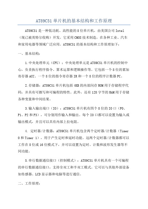
图 2 PLC 与单片机硬件连接图 1. 3 通信协议设计
要保证通信的 可 靠 和 有 条 不 紊,必 须 有 严 格 的 通 信协议。由于单片机采用串行通信方式,PLC 采用自 由口通信方式,给通信协议的设计带来极大的方便性。 根据需要本系统采用如下协议。
( 1) 通信波特率为 9. 6 kbps 无校验,8 个数据位,1 位起始位,1 位停止位。
void init_com( void) { TOMD = 0x20; / / 定时器 1,方式 2 自动装载 PCON = 0x00; / / SMOD = 0 SCON = 0x50; / / 方式 1,并且允许接收数据 TL1 = 0xfd; TH1 = 0xfd; / / 波特率为 9600bps TR1 = 1; / / 启动定时器 1 ES = 1; / / 串行中断允许 EA = 1; / / 全局中断允许 } 单片机在发送和接受数据过程中首先允许单片机 发送数据,然后将数据按字节写入缓冲区,数据全部写 完之后禁止发送数据并且允许接受数据。数据接收在 中断子程序中完成。 2. 2 PLC 通信程序设计 PLC 通信程序设计主要包括 PLC 通信端口初始 化、数据流生成、产生校验码和接收发送中断子程序。 ( 1) PLC 通信方式: PLC 自由口通信方式具有通信
Abstract That article describes the 51 MCU and S7 - 200 serial communication method,and uses a system composed of microcontroller and PLC to achieve displaying PLC's float data in the LCD,and can modify the data on the line and alarm,and the article gives the software and hardware realization. Key words S7 - 200 PLC 51 MCU serial communication
* 收稿日期: 2011 - 03 - 21 作者简介: 张兆营,临矿集团田庄矿机电科科长。
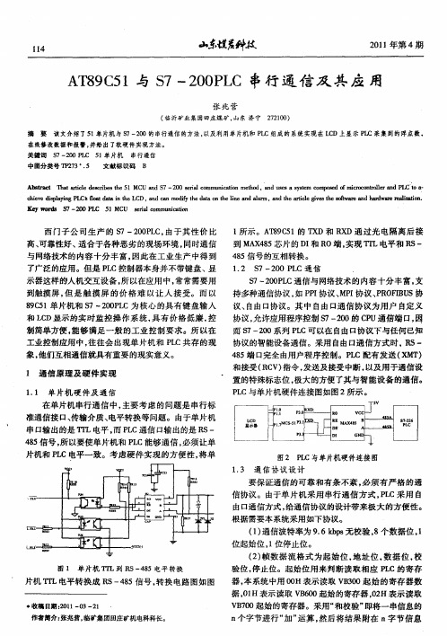
1 所示。AT89C51 的 TXD 和 RXD 通过光电隔离后接 到 MAX485 芯片的 DI 和 RO 端,实现 TTL 电平和 RS - 485 信号的互相转换。 1. 2 S7 - 200 PLC 通信
114
2011 年第 4 期
AT89C51 与 S7 - 200PLC 串行通信及其应用
张兆营
( 临沂矿业集团田庄煤矿,山东 济宁 272100)
摘 要 该文介绍了 51 单片机与 S7 - 200 的串行通信的方法,以及利用单片机和 PLC 组成的系统实现在 LCD 上显示 PLC 采集到的浮点数, 在线修改数据和报警,并给出了软硬件实现方法。 关键词 S7 - 200 PLC 51 单片机 串行通信 中图分类号 TP273 + . 5 文献标识码 B
方便,协议由用户自行设计等优点,便于和各种智能设 备通信。根据已经设定的通信协议在自由口初始化程 序中实现 PLC 端通信协议,并且将接收和发送数据放 在中断程序中实现,保证了通信的实时性。
MOVB 16 #09,SMB30 / / 设置 PORT0 为自由口通 信,波特率为 9600bps,无奇偶校验
MOVB 16#B0,SMB87 MOVB 16#FF,SMB89 / / 检测信息的结束字符 MOVW 5,SMW90 / / 检测空闲时间 MOVB 100,SMB94 / / 最多接收字符 ATCH INT_0: INT0,23 ATCH INT_2: INT2,9 ENI / / 开中断 RCV VB100,0 / / 接收缓冲区 ( 2) 通信数据流生成: 为了提高精确度,显示的数 据应该具有两位小数。由于 PLC 和单片机通信按字节 传送数据,因此需要将 PLC 采集到的数据( 实数) 转换 成整数,本程序采用截取的方式将 PLC 数据保留 2 位 小数,然后乘以 100 之后变成整数,调用分离算法将此 整数分成 4 个字节,每个字节代表实数的一个数字,按 从高位到低位的顺序送单片机。
在单片机串行 通 信 中,主 要 考 虑 的 问 题 是 串 行 标 准通信接口、传输介质、电平转换等问题。由于单片机 串口输出的是 TTL 电平,而 PLC 通信口输出的是 RS - 485 信号,所以要使单片机和 PLC 能够通信,必须让单 片机和 PLC 电平一致。考虑硬件实现的方便性,将单
图 1 单片机 TTL 到 RS - 485 电平转换 片机 TTL 电平转换成 RS - 485 信号,转换电路图如图
单片机采用 8 位异步串行通信方式,在该方式中 一帧信息为 10 位: 1 位起始位,8 位数据位,1 位停止 位,与 PLC 一帧信息格式一致。8051 系统中常采用定 时器 1 作为波特率发生器,其波特率由下式确定: 波特 率 = ( 定时 / 计数器 1 溢出率) / ( 32 / ) 。在通信之前首 先要对串口初始化,程序如下所示:
西门子公司生产的 S7 - 200PLC,由于其性价 比 高、可靠性好、适合于各种恶劣的现场环境,同时通信 与网络技术的 内 容 十 分 丰 富,因 此 在 工 业 生 产 中 得 到 了广泛的应用。但是 PLC 控制器本身并不带键盘、显 示器这样的人机交互设备,所以在应用中,常常需要用 到触摸 屏,但 是 触 摸 屏 的 价 格 难 以 让 人 接 受。而 以 89C51 单片机和 S7 - 200PLC 为核心的具有键盘输入 和 LCD 显示的实时监控操作系统,具有价格低廉,控 制简单方便,能 够 满 足 一 般 的 工 业 控 制 要 求。 所 以 在 工业控制应用中,往往会出现单片机和 PLC 共存的现 象,他们互相通信就具有重要的现实意义。 1 通信原理及硬件实现 1. 1 单片机硬件及通信
S7 - 200PLC 通信与网络技术的内容十分丰富,支 持多种通信协议,如 PPI 协议、MPI 协议、PROFIBUS 协 议、自由口协 议。 其 中 自 由 口 通 信 协 议 为 用 户 自 定 义 协议,允许应用程序控制 S7 - 200 的 CPU 通信端口,因 而 S7 - 200 系列 PLC 可以在自由口协议下与任何已知 协议的智能设备通信。采用自由口通信方式时,RS - 485 端口完全由用户程序控制。PLC 配受中断,以及用于通信设 置的特殊标志位,极大的方便了其与智能设备的通信。 PLC 与单片机硬件连接图如图 2 所示。
2011 年第 4 期
115
后面一起传送,来检测和排除干扰。 ( 3) 采用结束码来识别一帧数据的结束,本系统
采用 FFH 作为结束字符。
2 系统软件实现
AT89C51 和 S7 - 200 组 成 的 工 作 系 统 中,以 AT89C51 作为上位机,S7 - 200PLC 作为下位机。数据 的接收和发送由单片机控制 MAX485 芯片引脚实现。 PLC 通信口接到单片机发送的命令后,进入 PLC 中断 程序执行相应功能。 2. 1 单片机通信程序设计