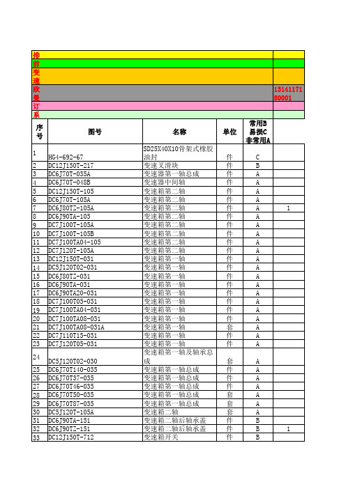
092J-5
变速箱配件明细
件
A
变速箱第一轴
件
A
变速箱第一轴
件
A
变速箱第一轴
件
A
变速箱第一轴
件
A
变速箱第一轴
件
A
变速箱第一轴
件
A
变速箱第一轴
套
A
变速箱第一轴
件
A
变速箱第一轴
件
A
变速箱第一轴及轴总
成
套
A
变速箱第一轴总成
件
A
变速箱第一轴总成
件
A
变速箱第一轴总成
件
A
变速箱第一轴总成
套
A
变速箱第一轴总成
套
A
变速箱二轴
套
A
变速箱二轴后轴承盖
13141171 80001
常用B
名称
单位 易损C
非常用A
SD25X40X10骨架式橡胶
油封
件
C
变速叉滑块
件
B
变速器第一轴总成
件
A
变速器中间轴
件
A
变速箱第二轴
件
A
变速箱第二轴
件
A
变速箱第二轴
件
A
1
变速箱第二轴
件
A
变速箱第二轴
件
A
变速箱第二轴
件
A
变速箱第二轴
件
A
变速箱第二轴
件
A
变速箱第一轴
件
A
变速箱第一轴
排 前 变 速 欧 曼 订 系
序 号
图号
1 HG4-692-67 2 DC12J150T-217 3 DC6J70T-035A 4 DC6J70T-048B 5 DC12J150T-105 6 DC6J70T-105A 7 DC6J80TZ-105A 8 DC6J90TA-105 9 DC7J100T-105A 10 DC7J100T-105B 11 DC7J100TA04-105 12 DC7J120T-105A 13 DC12J150T-031 14 DC5J120T02-031 15 DC6J80TZ-031 16 DC6J90TA-031 17 DC6J90TA20-031 18 DC7J100T05-031 19 DC7J100TA04-031 20 DC7J100TA08-031 21 DC7J100TA08-031A 22 DC7J110T15-031 23 DC7J120T05-031
【精品】焊接作业指导书2009hj005(p11)
焊接工艺规程编号
2009-HJ-009
页数
1OF2
焊接工艺评定报告编号PQR
焊接方法GTAW+SMAW
操作类型(手工,自动,半自动)手工
焊接接头:
坡口形式V型材料及规格Φ159*6。0
简图:
60°±5°
2±1/2
2±0。5
母材:
材料标准GB/T8163-87类型或牌号20
类、组别号Ⅰ-1与类、组别号相焊Ⅰ-1
焊接作业指导书
焊接工艺规程编号
2009-HJ-009
页数
2OF2
焊接位置:5G
对接焊缝位置平立向上、仰
焊接方向向上
角焊缝位置平立向上、仰
焊接方向
预热温度
层间温度
其它
焊后热处理:
温度范围
时间
气体:
气体混合比流量
保护气体Ar99.99%7—12L/min
尾部气
背部气
电特性:
电流种类:DC极性SP/RP电流范围(A)9~130(A)
3
SMAW
J427
φ3.2
DCSP
9~120
22~16
6.0~10.0
焊接技术:
摆动焊或不摆动焊:摆动
焊前清理和层间清理:砂轮机背面清根方法:
单道焊或多道焊(每面):多道焊单丝焊或多丝焊:
导电嘴至工件距离(mm):5~10mm锤击:
其他Other:
管子直径、厚度对接缝159mmδ=6.0mm
焊缝金属厚度范围:对接焊缝3.5~9.5mm
其它
焊材标准
ASTM20
ASTM20
焊材牌号
H08Mn2SiA
J427
GFJC092与计算机连用的显示设备、投影仪_0905_类产品工厂检查作业指导书080303.

GB7247.1
元
激光辐射(8)
一次/年 一次/年
3000V,1min,输入与输出间。 耐压测试仪。 初次极间爬电距离与电气间隙 符合 GB4943 中加强绝缘的要 求。
量具 目测 耐压仪 绝缘电阻测试仪 万用表 电源、温升测试记录仪
充放电试验装置
目测应有 1.6 要求的标志
目测
耐压仪
绝缘电阻测试仪 拉力、弯曲、扭力试验设备 目视,产品名称和型号规格 风扇应放置在铺有一层包装薄 棉纸的木质台板上,然后在风扇 上覆盖一层质量约 40g/m2 的漂 白棉纱布.然后,风扇应在其工 作电压下以堵转方式工作 7h, 或者一直工作到达稳定状态为 止(取其中时间较长者).试验结 束时,包装薄棉纸或纱布不应被 引燃
用电涌试验仪试验,不进行湿 热试验,电涌试验前后阻值变 化不大于 20%。
目测
用激光辐射测试仪测试
CQC/GF.JC092-2005
版 号:1
与计算机连用的显示设备、投影仪
(0905)类产品工厂检查作业指导书
修 订:1 修订日期:2008-03-03
第 9 页 共 16 页
压敏电阻器/ 电涌抑制器
用垂直/水平燃烧器试验,应符 合相应等级的要求(与型式试 验报告中的可燃性等级相同)。
CQC/GF.JC092-2005
版 号:1
与计算机连用的显示设备、投影仪
(0905)类产品工厂检查作业指导书
修 订:1 修订日期:2008-03-03
第 7 页 共 16 页
外壳、装饰件
.可燃性
GB4943
(附录 A)
电源开关(含 抗电强度 15 继电器开关)
发热 16
GB15092. 一次/年 1
08BJ2-5墙身-轻钢龙骨纸面石膏板(2007)共5部分-第1部分

工程设计文件8BJ2-5 墙身一轻胡龙骨(2007) 纸面石膏板华北地区建筑设计标准化办公室.妄■日由宀坨芒西北地区建筑标准设计协作办公室芸豕上申疋推存墙身一加气混凝土被取代原88J第1版已被停止使用的图集2007年5月班廬=禺(第2版)墙身-轻钢龙骨纸面石膏板(2007)前言88J是我们编制的建筑构造标准(通用)图集,是建筑设计文件的一部分。
早期的标准设计文件曾以蓝图形式出现。
随着建筑规模的扩大,使用量的增多,这种方式及图版规格不能满足使用需要,逐渐形成现在全国普遍釆用的标准设计文件形态,但其功能性质不变,仍是设计文件的一部分。
本图集自上世纪问世以来,已历时十余年。
在此期间获得了广大用户的支持与关心,收到了各方面的建议和意见。
鉴于新的建筑材料和建筑技术不断出现,一些标准和规范也有修改,为此,我们在听取各方面意见后,决定在新世纪初实施全面的二次修编。
二次修编原则仍如既往规定,即(一)以满足常用的一般标准的民用建筑构造为主,适当兼顾部分较高标准的需要。
(二)尽量反映新技术新材料的发展状况。
(三)力求适应工厂化配件制品的发展,并在图集附录中提供部分产品情况。
(四)努力做到构造技术先进,材料选用适当,品种类型多样,设计采用方便•由于“88J ”已在国家商标局进行商标注册,已经不是编制年份的含义。
故2001年开始的第二次修编,仍沿用“88J”的名称。
为便于区别,在前言上以“第2版”表示,敬请用户注意。
关于图集的编排次序,凡与初编图内容相同者,均用原册号. 凡新增内容的各册序号,均在后排列。
同时在各册序号后增加“―X”小序列,表示该册内容中有若干分册。
例如:“88J2—1”, 前面的“2 ”字表示墙身册的序号,而后列的小序列“-1 ”表示墙身册的第1分册,“一2 "为墙身册的第2分册……在进行二次修编时将对初编图进行筛选,或淘汰或继续使用,在各册中将分别说明•考虑到标准设计图集属推荐性标准,而非强制性标准,不应用行政手段推行地区性保护政策。
欧际接头
750 1109M03∗ 1109N03∗ 1109MN03∗ 1/2NPT
11 52 22 50 74 32 46
1109M00∗ 1109N00∗ 1109MN00∗ M22 1.5
1209M01∗ 1209N01∗ 1209MN01∗ G3/4"
650 1209M03∗ 1209N03∗ 1209MN03∗ 3/4NPT
300 20
20S09D∗ 20S09C∗ 20S099∗ M30 2 16 10.5 141 95 81 26 55 41 1200
300 25
25S09D∗ 25S09C∗ 25S099∗ M36 2 18 12 145 97 83 26 55 41 1200
300 30
30S09D∗ 30S09C∗ 30S099∗ M42 2 20 13.5 149 99 85 26 55 45 1200
15 62 29 62 93 41 55
1209M00∗ 1209N00∗ 1209MN00∗ M27 1.5
1709M01∗ 1709N01∗ 1709MN01∗ G1"
450 1709M03∗ 1709N03∗ 1709MN03∗ 1NPT
17 69 36 71 103 41 63
1709M00∗ 1709N00∗ 1709MN00∗ M33 1.5
96 70 48 38.5 30 98 71 49 38.5 30
18
18L092∗ 18L091∗ 18L0912∗ M26 1.5 12 7.5 131 99 65 54
41
22
22L092∗ 22L091∗ 22L0912∗ M30 2
14 7.5 135 101 67 54
HCPL-9031中文资料

Agilent HCPL-9000/-0900, -9030/-0930,HCPL-9031/-0931, -900J/-090J,HCPL-901J/-091J, -902J/-092J High Speed Digital Isolators Data SheetDescriptionThe HCPL-90xx and HCPL-09xx CMOS digital isolators feature high speed performance and excellent transient immunity specifications. The symmetric magnetic coupling barrier gives these devices a typical pulsewidth distortion of 2ns, a typical propagation delay skew of 4ns and 100 Mbaud data rate, making them the industry ’s fastest digital isolators.The single channel digital isola-tors (HCPL-9000/-0900) features an active-low logic output enable.The dual channel digital isolators are configured as unidirectional (HCPL-9030/-0930) and bi-directional (HCPL-9031/-0931),operating in full duplex mode making it ideal for digital fieldbus applications.The quad channel digital isola-tors are configured as unidirec-Features•+3.3V and +5V TTL/CMOS compatible• 3 ns max. pulse width distortion • 6 ns max. propagation delay skew•15 ns max. propagation delay•High speed: 100 MBd •15 kV/µs min. common mode rejection•Tri-state output (HCPL-9000/-0900)•2500V RMS isolation•UL1577 and IEC 61010-1 approvedApplications•Digital fieldbus isolation •Multiplexed data transmission •Computer peripheral interface •High speed digital systems •Isolated data interfaces •Logic level shiftingtional (HCPL-900J/-090J), two channels in one direction and two channels in opposite direc-tion (HCPL-901J/-091J), and one channel in one direction and three channels in opposite direction (HCPL-902J/-092J).These high channel density make them ideally suited to isolating data conversion devices, parallel buses and peripheral interfaces.They are available in 8-pin PDIP,8-pin Gull Wing, 8-pin SOIC packages, and 16–pin SOIC narrow-body and wide-bodypackages. They are specified over the temperature range of -40°C to +100°C.CAUTION: It is advised that normal static precautions be taken in handling and assembly of this component to prevent damage and/or degradation,which may be induced by ESD.Selection GuideDevice Number Channel Configuration PackageHCPL-9000Single8-pin DIP (300 Mil)HCPL-0900Single8-pin Small OutlineHCPL-9030Dual8-pin DIP (300 Mil)HCPL-0930Dual8-pin Small OutlineHCPL-9031Dual, Bi-Directional8-pin DIP (300 Mil)HCPL-0931Dual, Bi-Directional8-pin Small OutlineHCPL-900J Quad16-pin Small Outline, Wide Body HCPL-090J Quad16-pin Small Outline, Narrow Body HCPL-901J Quad, 2/2, Bi-Directional16-pin Small Outline, Wide Body HCPL-091J Quad, 2/2, Bi-Directional16-pin Small Outline, Narrow Body HCPL-902J Quad, 1/3, Bi-Directional16-pin Small Outline, Wide Body HCPL-092J Quad, 1/3, Bi-Directional16-pin Small Outline, Narrow BodyOrdering InformationSpecify Part Number followed by Option Number (if desired). Examples:HCPL-90xx-xxxxxx:No option = 300 Mil PDIP-8 package, 50 units per tube.300 = Gull Wing Surface Mount Option, 50 units per tube.500 = Tape and Reel Packaging Option, 1000 units per reel.HCPL-09xx-xxxxxx:No option = SO-8 package, 100 units per tube.500 = Tape and Reel Packaging Option, 1500 units per reel.HCPL-90xJ-xxxxxx:No option = Wide Body SOIC-16 package, 50 units per tube.500 = Tape and Reel Packaging Option, 1000 units per reel.HCPL-09xJ-xxxxxx:No option = Narrow Body SOIC-16 package, 50 per tube.500 = Tape and Reel Packaging Option, 1000 units per reel.Pin DescriptionSymbol DescriptionVDD1Power Supply 1VDD2Power Supply 2IN X Logic Input Signal OUT X Logic Output Signal GND1Power Supply Ground 1GND2Power Supply Ground 2V OE Logic Output Enable (Single Channel), Active LowNC Not Connected Functional DiagramsTruth TableIN1V OE OUT1L L LH L HL H ZH H ZV DD1IN1NCGND1GND2OUT1V DD2V OEHCPL-9000/0900Single ChannelDual ChannelV DD1IN1IN2GND1GND2OUT2V DD2OUT1HCPL-9030/0930Quad ChannelV DD1GND1IN1IN2IN3IN4NCGND1GND2NCOUT4OUT3OUT2OUT1GND2V DD2HCPL-900J/-090JV DD1GND1IN1IN2OUT3OUT4NCGND1GND2NCIN4IN3OUT2OUT1GND2V DD2HCPL-901J/-091JV DD1GND1IN1IN2IN3OUT4NCGND1GND2NCIN4OUT3OUT2OUT1GND2V DD2HCPL-902J/-092JV DD1IN1OUT2GND1GND2IN2V DD2OUT1HCPL-9031/0931Package Outline DrawingsHCPL-9000, HCPL-9030 and HCPL-9031 Standard DIP PackagesHCPL-9000, HCPL-9030 and HCPL-9031 Gull Wing Surface Mount Option 300BSCDIMENSIONS INCHES (MILLIMETERS)LEAD COPLANARITY = 0.004 INCHES (0.10 mm)MIN MAXDIMENSIONS: INCHES (MILLIMETERS)MINMAXDIMENSIONS: INCHES (MILLIMETERS)MINMAXHCPL-0900, HCPL-0930 and HCPL-0931 Small Outline SO-8 PackageHCPL-900J, HCPL-901J and HCPL-902J Wide Body SOIC-16 Package0.092 (2.337)0.104 (2.642)0.011 (0.279)°DIMENSIONS: INCHES (MILLIMETERS)MINMAXHCPL-090J, HCPL-091J and HCPL-092J Narrow Body SOIC-16 Package0.054 (1.372)0.068 (1.727)0.010 (0.249)DIMENSIONS: INCHES (MILLIMETERS)MINMAXPackage CharacteristicsParameter Symbol Min.Typ.Max.Units Test ConditionsCapacitance (Input-Output)[1]CI-OpF f = 1 MHzSingle Channel 1.1Dual Channel 2.0Quad Channel 4.0Thermal ResistanceθJCT°C/W Thermocouple located at8-Pin PDIP150center underside of package 8-Pin SOIC240Package Power Dissipation P PD mW8-Pin PDIP1508-Pin SOIC150Notes:1.Single and dual channels device are considered two-terminal devices: pins 1-4 shorted and pins 5-8 shorted. Quad channel devices are consideredtwo-terminal devices: pins 1-8 shorted and pins 9-16 shorted.This product has been tested for electrostatic sensitivity to the limits stated in the specifications. However, Agilent recommends that all integrated circuits be handled with appropriate care to avoid damage. Damage caused by inappropriate handling or storage could range from performance degradation to complete failure.Insulation and Safety Related SpecificationsParameters Condition Min.Typ.Max.UnitsBarrier ImpedanceΩ||pF Single Channel>1014||3Dual Channel>1014||3Quad Channel>1014||7Creepage Distance (External)mm8-Pin PDIP7.0368-Pin SOIC 4.02616-Pin SOIC Narrow Body 4.02616-Pin SOIC Wide Body8.077Leakage Current240 VRMS 0.2µA60 HzAbsolute Maximum RatingsParameters Symbol Min.Max.Units Storage Temperature T S–55175°C Ambient Operating Temperature[1]T A–55125°C Supply Voltage V DD1, V DD2–0.57VInput Voltage VIN –0.5VDD1+0.5VVoltage Output Enable (HCPL-9000/-0900)V OE–0.5V DD2 +0.5VOutput Voltage V OUT–0.5V DD2 +0.5VOutput Current Drive I OUT10mALead Solder Temperature (10s)260°CESD 2 kV Human Body ModelNotes:1.Absolute Maximum ambient operating temperature means the device will not be damaged if operated under these conditions. It does notguarantee performance.Recommended Operating ConditionsParameters Symbol Min.Max.UnitsAmbient Operating Temperature T A–40100°CSupply Voltage V DD1, V DD2 3.0 5.5VLogic High Input Voltage V IH 2.4V DD1VLogic Low Input Voltage V IL00.8VInput Signal Rise and Fall Times tIR , tIF1µsThis product has been tested for electrostatic sensitivity to the limits stated in the specifications. However, Agilent recommends that all integrated circuits be handled with appropriate care to avoid damage. Damage caused by inappropriate handling or storage could range from performance degradation to complete failure.Electrical SpecificationsTest conditions that are not specified can be anywhere within the recommended operating range.All typical specifications are at T A=+25°C, V DD1 = V DD2 = +3.3V.Parameter Symbol Min.Typ.Max.Units Test ConditionsQuiescent Supply Current 1I DD1mA V IN = 0VHCPL-9000/-09000.0080.01HCPL-9030/-09300.0080.01HCPL-9031/-0931 1.5 2.0HCPL-900J/-090J0.0160.02HCPL-901J/-091J 3.3 4.0HCPL-902J/-092J 1.5 2.0Quiescent Supply Current 2I DD2mA V IN = 0VHCPL-9000/-0900 3.3 4.0HCPL-9030/-0930 3.3 4.0HCPL-9031/-0931 1.5 2.0HCPL-900J/-090J 5.58.0HCPL-901J/-091J 3.3 4.0HCPL-902J/-092J 3.0 6.0Logic Input Current I IN -1010µALogic High Output Voltage V OH V DD2–0.1 V DD2V I OUT = -20 µA, V IN=V IH0.8*V DD2 V DD2–0.5V I OUT = -4 mA, V IN=V IHLogic Low Output Voltage V OL 00.1V I OUT = 20 µA, V IN=V IL0.5 0.8V I OUT = 4 mA, V IN=V IL Switching SpecificationsMaximum Data Rate100110MBd C= 15 pFLClock Frequency fmax50MHzPropagation Delay Time to Logic t PHL1218nsLow OutputPropagation Delay Time toLogic t PLH1218nsHigh OutputPulse Width t PW10nsPulse Width Distortion[1]|PWD|23ns|t PHL– t PLH|Propagation Delay Skew[2]t PSK46nsOutput Rise Time (10–90%)t R24nsOutput Fall Time (10–90%)t F24nsPropagation Delay Enable to Output (Single Channel)High to High Impedance t PHZ35nsLow to High Impedance t PLZ35nsHigh Impedance to High t PZH35nsHigh Impedance to Low t PZL35nsChannel-to-Channel Skew t CSK23ns(Dual and Quad Channels)Common Mode Transient Immunity|CM H|1518kV/µs V cm = 1000V(Output Logic High or Logic Low)[3]|CM L|Notes:1.PWD is defined as |t PHL -t PLH|. %PWD is equal to the PWD divided by the pulse width.2.t PSK is equal to the magnitude of the worst case difference in t PHL and/or t PLH that will be seen between units at 25°C.3.CM H is the maximum common mode voltage slew rate that can be sustained while maintaining V OUT > 0.8V DD2. CM L is the maximum common modeinput voltage that can be sustained while maintaining V OUT < 0.8V. The common mode voltage slew rates apply to both rising and falling common mode voltage edges.This product has been tested for electrostatic sensitivity to the limits stated in the specifications. However, Agilent recommends that all integrated circuits be handled with appropriate care to avoid damage. Damage caused by inappropriate handling or storage could range from performance degradation to complete failure.Electrical SpecificationsTest conditions that are not specified can be anywhere within the recommended operating range.All typical specifications are at T A=+25°C, V DD1 = V DD2 = +5.0V.Parameter Symbol Min.Typ.Max.Units Test ConditionsQuiescent Supply Current 1I DD1mA V IN = 0VHCPL-9000/-09000.0120.018HCPL-9030/-09300.0120.018HCPL-9031/-0931 2.5 3.0HCPL-900J/-090J0.0240.036HCPL-901J/-091J 5.0 6.0HCPL-902J/-092J 2.5 3.0Quiescent Supply Current 2I DD2mA V IN = 0VHCPL-9000/-0900 5.0 6.0HCPL-9030/-0930 5.0 6.0HCPL-9031/-0931 2.5 3.0HCPL-900J/-090J8.012.0HCPL-901J/-091J 5.0 6.0HCPL-902J/-092J 6.09.0Logic Input Current I IN -1010µALogic High Output Voltage V OH V DD2–0.1 V DD2V I OUT= -20 µA, V IN=V IH0.8*V DD2 V DD2 –0.5V I OUT= -4 mA, V IN=V IHLogic Low Output Voltage V OL 00.1V I OUT= 20 µA, V IN=V IL0.5 0.8V I OUT= 4 mA, V IN=V IL Switching SpecificationsMaximum Data Rate100110MBd C= 15 pFLClock Frequency fmax50MHzPropagation Delay Time to Logic t PHL1015nsLow OutputPropagation Delay Time to Logic t PLH1015nsHigh OutputPulse Width t PW10nsPulse Width Distortion[1]|PWD|23ns|t PHL– t PLH|Propagation Delay Skew[2]t PSK46nsOutput Rise Time (10–90%)t R13nsOutput Fall Time (10–90%)t F13nsPropagation Delay Enable to Output (Single Channel)High to High Impedance t PHZ35nsLow to High Impedance t PLZ35nsHigh Impedance to High t PZH35nsHigh Impedance to Low t PZL35nsChannel-to-Channel Skew t CSK23ns(Dual and Quad Channels)Common Mode Transient Immunity|CM H|1518kV/µs V cm = 1000V(Output Logic High or Logic Low)[3]|CM L|Notes:1.PWD is defined as |t PHL -t PLH|. %PWD is equal to the PWD divided by the pulse width.2.t PSK is equal to the magnitude of the worst case difference in t PHL and/or t PLH that will be seen between units at 25°C.3.CM H is the maximum common mode voltage slew rate that can be sustained while maintaining V OUT > 0.8V DD2. CM L is the maximum common modeinput voltage that can be sustained while maintaining V OUT < 0.8V. The common mode voltage slew rates apply to both rising and falling common mode voltage edges.This product has been tested for electrostatic sensitivity to the limits stated in the specifications. However, Agilent recommends that all integrated circuits be handled with appropriate care to avoid damage. Damage caused by inappropriate handling or storage could range from performance degradation to complete failure.Applications InformationPower ConsumptionThe HCPL-90xx and HCPL-09xx CMOS digital isolators achieves low power consumption from the manner by which they transmit data across isolation barrier. By detecting the edge transitions of the input logic signal and con-verting this to a narrow current pulse, which drives the isolation barrier, the isolator then latches the input logic state in the output latch. Since the current pulses are narrow, about 2.5ns wide, the power consumption is indepen-dent of mark-to-space ratio and solely dependent on frequency.The approximate power supply current per channel is:I(Input) = 40(f/fmax)(1/4)mA where f = operating frequency,fmax =50MHz.Signal Status on Start-up and Shut DownTo minimize power dissipation,the input signals to the channels of HCPL-90xx and HCPL-09xx digital isolators are differenti-ated and then latched on the output side of the isolationbarrier to reconstruct the signal.This could result in an ambigu-ous output state depending on power up, shutdown and power loss sequencing. Therefore, the designer should consider the inclusion of an initialization signal in this start-up circuit.Bypassing and PC Board Layout The HCPL-90xx and HCPL-09xx digital isolators are extremely easy to use. No external interface circuitry is required because the isolators use high-speed CMOS IC technology allowing CMOS logicto be connected directly to the inputs and outputs. As shown in Figure 1, the only externalcomponents required for proper operation are two 47nF ceramic capacitors for decoupling the power supplies. For each capaci-tor, the total lead length between both ends of the capacitor and the power-supply pins should notexceed 20 mm. Figure 2 illustrates the recommended printed circuit board layout for the HCPL-9000or HCPL-0900. For data rates in excess of 10MBd, use of ground planes for both GND 1 and GND 2 is highly recommended.Figure 1. Functional Diagram of Single Channel HCPL-0900 or HCPL-0900.V DD1IN Note: C1, C2 = 47 nF ceramic capacitorsDD2OUT 1Figure 2. Recommended Printed Circuit Board Layout.C2V DD2OUT 1GND 2V DD1GND 1IN 1C1V OEHCPL-9000or HCPL-090011Propagation Delay, Pulse WidthDistortion and Propagation Delay Skew Propagation Delay is a figure of merit, which describes howquickly a logic signal propagates through a system as illustrated in Figure 3.The propagation delay from low to high, t PLH , is the amount of time required for an input signal to propagate to the output, causing the output to change from low to high. Similarly, the propagation delay from high to low, t PHL , is the amount of time required for the input signal to propagate to the output, causing the output to change from high to low.Figure 3. Timing Diagrams to Illustrate Propagation Delay, t PLH and t PHL .Figure 4. Timing Diagrams to Illustrate Propagation Delay Skew.VV V V Pulse Width Distortion, PWD, is the difference between t PHL and t PLH and often determines the maximum data rate capability of a transmission system. PWD can be expressed in percent bydividing the PWD (in ns) by the minimum pulse width (in ns)being transmitted. Typically, PWD on the order of 20–30% of the minimum pulse width is tolerable.Propagation Delay Skew, t PSK ,and Channel-to-Channel Skew,t CSK , are critical parameters to consider in parallel data trans-mission applications where synchronization of signals on parallel data lines is a concern.If the parallel data is being sent through channels of the digital isolators, differences in propaga-tion delays will cause the data to arrive at the outputs of the digital isolators at different times. If this difference in propagation delay is large enough, it will limit the maxi-mum transmission rate at which parallel data can be sent through the digital isolators.t PSK is defined as the difference between the minimum and maximum propagation delays,either t PLH or t PHL , among two or more devices which are operating under the same conditions (i.e.,the same drive current, supply voltage, output load, and operat-ing temperature). t CSK is defined as the difference between theminimum and maximum propaga-tion delays, either t PLH or t PHL ,among two or more channelswithin a single device (applicable to dual and quad channel de-vices) which are operating under the same conditions.As illustrated in Figure 4, if the inputs of two or more devices are switched either ON or OFF at the same time, t PSK is the difference between the minimum propaga-tion delay, either t PLH or t PHL , and the maximum propagation delay,either t PLH or t PHL .As mentioned earlier, t PSK , can determine the maximum parallel data transmission rate. Figure 5shows the timing diagram of a typical parallel data transmission application with both the clock and data lines being sent through the digital isolators. The figure shows data and clock signals at the inputs and outputs of the digital isolators. In this case, thedata is clocked off the rising edge of the clock.Figure 5. Parallel Data Transmission.DATADATAINPUTSCLOCKOUTPUTSCLOCKINPUTOUTPUT5 V CMOS2.5 V CMOS 0 VV OHV OLV OUTV IN/semiconductorsFor product information and a complete list of distributors, please go to our web site.For technical assistance call:Americas/Canada: +1 (800) 235-0312 or (408) 654-8675Europe: +49 (0) 6441 92460China: 10800 650 0017Hong Kong: (+65) 6271 2451India, Australia, New Zealand: (+65) 6271 2394Japan: (+81 3) 3335-8152(Domestic/International), or 0120-61-1280(Domestic Only)Korea: (+65) 6271 2194Malaysia, Singapore: (+65) 6271 2054Taiwan: (+65) 6271 2654Data subject to change.Copyright © 2002 Agilent Technologies, Inc.October 31, 20025988-5626ENPropagation delay skew repre-sents the uncertainty of where an edge might be after being sent through a digital isolator. Figure 5 shows that there will be uncer-tainty in both the data and clock lines. It is important that these two areas of uncertainty not overlap, otherwise the clock signal might arrive before all of the data outputs have settled, or some of the data outputs may start to change before the clock signal has arrived. From these considerations, the absoluteminimum pulse width that can be sent through digital isolators in a parallel application is twice t PSK .A cautious design should use a slightly longer pulse width toFigure 6. Timing Diagrams to Illustrate the Minimum Pulse Width, Rise and Fall Time, and Propagation Delay Enable to Output Waveforms for HCPL-9000 or HCPL-0900.ensure that any additional uncertainty in the rest of the circuit does not cause a problem.Figure 6 shows the minimum pulse width, rise and fall time,and propagation delay enable to output waveforms for HCPL-9000or HCPL-0900.t PW Minimum Pulse Width t PHZ Propagation Delay, High to High Impedance t PLZ Propagation Delay, Low to High Impedance t PZL Propagation Delay, High Impedance to Low t PZH Propagation Delay, High Impedance to High t R Rise Time t F Fall Time。
给水排水管道工程质量评定表

水利水电工程给水排水管道工程施工及验收规范单元工程质量评定表目录J1沟槽开挖与地基处理单元工程质量评定表 (4)J2刚性管道沟槽回填单元工程质量评定表 (7)J3柔性管道沟槽回填单元工程质量评定表 (9)J4管道沟槽回填单元工程质量评定表 (10)J5管道沟槽回填(球墨铸铁管)单元工程质量评定表 (11)J6管道沟槽回填(钢筋混凝土管)单元工程质量评定表 (12)J7管道沟槽回填(钢管)单元工程质量评定表 (13)J8管道基础单元工程质量评定表 (14)J9钢管内防腐层(水泥砂浆)单元工程质量评定表 (16)J10钢管内防腐层(液体环氧涂料)单元工程质量评定表 (17)J11钢管接口连接单元工程质量评定表 (18)J12钢管外防腐层单元工程质量评定表 (19)J13钢管阴极保护单元工程质量评定表 (20)J14球墨铸铁管接口连接单元工程质量评定表 (21)J15钢筋混凝土管、预(自)应力混凝土管、预应力钢筒混凝土管 (23)J16接口连接单元工程质量评定表 (23)J17钢筋混凝土管接口单元工程质量评定表 (24)J18钢筋混凝土管接口连接单元工程质量评定表 (25)J19化学建材管接口连接单元工程质量评定表 (26)J20管道铺设单元工程质量评定表 (27)J21管道铺设(钢管)单元工程质量评定表 (28)J22管道铺设(球墨铸铁管)单元工程质量评定表 (29)J23管道铺设(钢筋混凝土管)单元工程质量评定表 (30)J24工作井单元工程质量评定表 (31)J25直线顶管管道单元工程质量评定表 (33)J26曲线顶管管道单元工程质量评定表 (35)J27垂直顶升管道单元工程质量评定表 (37)J28盾构管片制作单元工程质量评定表 (38)J29盾构掘进和管片拼装单元工程质量评定表 (40)J30盾构施工管道的钢筋混凝土二次衬砌单元工程质量评定表 (42)J31浅埋暗挖管道的土层开挖单元工程质量评定表 (43)J32浅埋暗挖管道的初期衬砌单元工程质量评定表 (44)J33浅埋暗挖管道的防水层单元工程质量评定表 (46)J34浅埋暗挖管道的二次衬砌单元工程质量评定表 (47)J35定向钻施工管道单元工程质量评定表 (48)J36夯管施工管道单元工程质量评定表 (50)J37沉管基槽浚挖及管基处理单元工程质量评定表 (51)J38组对拼装管道(段)的沉放单元工程质量评定表 (51)J39沉放的预制钢筋混凝土管节制作单元工程质量评定表 (53)J40沉放的预制钢筋混凝土管节接口预制加工单元工程质量评定表 (54)J41预制钢筋棍凝土管的沉放单元工程质量评定表 (55)J42沉管的稳管及回填单元工程质量评定表 (56)J43桥管管道单元工程质量评定表 (57)J44井室单元工程质量评定表 (59)J45雨水口及支、连管单元工程质量评定表 (61)J46支墩单元工程质量评定表 (62)J47铸铁管(承插口)安装单元工程质量评定表 (63)表B.0.2分项工程质量验收记录表 (65)表B.0.3分部(子分部)工程质量验收记录表 (66)表B.0.4-1单位(子单位)工程质量竣工验收记录表 (67)表B.0.4-2单位(子单位)工程质量控制资料核查表 (68)表B.0.4-3单位(子单位)工程观感质量核查表 (69)表B.0.4-4单位(子单位)工程结构安全和使用功能性检测记录表 (70)表C.0.3注水法试验记录表 (71)表D.0.2管道闭水试验记录表 (72)表E.0.2管道闭气检验记录表 (73)水利水电工程J1沟槽开挖与地基处理单元工程质量评定表注:本表验收标准引用GB50268-2008《给排水管道工程施工及验收规范》。
万能遥控器代码一览表
国内电视: flV<iAGg长虹 000. 008. 009. 091. 092. 093. 010. 011. 014. 016 .026. 028. 033. 051. 088.100.157.158.159. 160. 161. 180 .181. 185 .186 .191. 192 .210. 211. 212. 229. 230 .231 .232 5vg9 oTtS9康佳 011 .017 .029 .032 .034.054 .067 .069 .071 .075 .076 .077 .078 .079 .080 .081 107 113 117. 173 .174. 175. 176. 189. 201. 202. 203. 217 .218. 220. 226 .267.236 $ K d{V $创维 011. 025.033.045.046.060 .070. 017 .072. 073. 074. 079.083.010 .107. 108 .109 162 163 .164 .165 .166 .167. 168. 169. 177. 224.225. 235. 246 R LH \f熊猫 001. 011. 016. 021. 022. 023 .024 .025. 026. 028 .033 .040 .043. 053. 056.009. 057. 058 051. 061. 062.073. 079. 089.091 .124 .125 .234.237. 238. 239 .240.241.242. 243. 244 245 247.248 .249 .250. 251 ^V'gSvTCL 051.053 .068. 071 .073. 082 .083.084 .085. 110 .111 .170 .171. 172.178. 179 .187.188.197 .198.199. 200 .233 , z n;`海尔 103 .112 .118 .119. 150. 151 .152 .153 .154 .155 .156. 182. 183. 184. 193. 194 .213 .228 6 yPf%1&s海信 000. 006 .007. 008. 010 .014 .015. 025. 045. 046 .103. 105.107 .115 .116 .128. 129.130.131138 .139.150 .151 .152 .153 .154 .155 .156 .182 .183 .184 .193 .194 .213 .228 2i 7OP0T金星 007. 008. 011 .013. 024. 025. 032. 033 .039 .051 .065 .071 .073. 079 .091 .097 .138 HXe y福日 007 .011 .015 .023.024. 028. 033. 034. 040. 043. 053. 056.060 .061 .065 .079 k%c c$B安华ANHUA 017. 001. 032. 047 8ML G"百花BAIHUA 016. 025 .033 .053. 056. 079 LtV <w&zp百合花BAIHEHUA 023. 024. 040. 043 YQ hFG百乐BAILE 016. 025. 012 .019. 026. 027.028. 029 .030. 031. 042 9 E6GF~j2宝声BAOSHENG 011. 025. 016 <%\ qDmN北京 008 .012.011. 019 .016. 023. 024. 025. 027 .028.029 .030. 031.033 .044 .043 .050 .053 .056 .026 .079.091 .039. 042.051. 021. 122 .126 `> XDqWc宝花石BaoHuaShi 033.053.056. 079 " BkO.>x彩虹CAIHONG 011. 025. 016 vgd 62<TF彩星 CAIXING 023. 024. 040 .043 4g LAZ V长城 011 .016 .017. 023 .024 .025.033. 040 .043 .053. 056 .001 .012. 029 .027 .026.028 .029.030 :5b V |-031 .042. 079 Fy pR$wd海虹HAIHONG 016 .025 .026 .027. 028 .029 .030 wH DYBx b海乐HAILE 032. 047 Y~C:G R$r海燕HAIYAN 011. 023. 024 .033. 040. 043.053 .056. 079 D$s2|Ek环宇HUANY 011.015. 023. 024. 033 .040. 043. 053. 056 .009. 057.058 %K5-&PK4L虹美HONGMEI 003. 011. 016 .018 .023. 024. 025 .033 .040. 043. 056. 009.057 .058. 079 8L ew 3红岩HONGYAN 011.033. 053. 056. 079 36s,} 5D菊花JUHUA 011.023.024.033.040.43.053.056.079 bf, fj IW金海 JINHAI 009.057.058 cgw/{G{%j金凤JINFENG 001.011.021.022 guv t l金塔JINTA 016.023.024.025.033.040.043.053.056.009.057.058.079 o$ ~YrsZ金鹊 JINQUE 011.025.016 <8 v S e金雀JINQUE 032.033.053.056.079 uuwH b xe嘉华JIAHUA 017.047.001.032 >8BA| U'昆仑KUNLUN 001.011.021.022.033.025.012.042.040.039 ;M$ C |凯歌KAIGE 011.016.023.024.025.033.040.043.053.056.079 -vFvmSf:9n康力KANGLI 027.012.019.025.026.028.030.031.033.120 W,h R_&vl康虹KANGHONG 009.058.057 K BR Hf康立KANGLI 016.023024.025.040.043.011.026.029.042.005 _ i"` 9|Y康艺KANGYI 016.025.033.053.056.079.121 Vl_x IM22孔雀KONGQUE 011.016.023.024.025.033.040.041.043.124 e F b\Yp B快乐KUAILE 016.025.033.053.056.079 Io kT>:乐华ROWA 011.016.023.024.025.040.043.096.127 h> }%2 s龙江LONGJIANG 011.033.053.056.079 T \ ix_利华LIHUA 011 R -'xEU牡丹MUDAN001.002.011.016.020.021.022.025.032.033.040.043.053.056.059.063.065.079 :WU`tk X美乐MEILE 011.023.024.033.040.043.053.056.009.057.058.079 Pa Q cI vG梦寐MENGMEI 023.024.040.043 B 3\ $南声NANSHENG 011.033.053.056.079 1 Y TE青岛QINGDAO 001.011.021.022.033.053.056.079 g p7N2m/如意RUYI 011.015.023.024.040.043 OS" xR ly神彩SHENCAI 007.016.025.033.053.056.079 U= 1|2}L山茶SHANGCAI 011.033.053.056.079 }chXUsR_/s上海SHANGHAI011.016.017.022.023.024.025.033.040.043.0053.056.009.057.058.079.123 ^ %S8 Ye韶峰SHAOFENG 011.015.000.006.007.023 >; ^=bxbQ沈阳SHENGYAN 011.016.025.046.045.033 TV \C4^x_塞格SAIGE 011.025.016 h~Ub OsI$松柏SONGBA 016.025 M6qS3 B"-h三元SANYUAN 003.011.016.018.023.024.025.040.043 {3 H Ne,X三键SANJIAN 033.053.056.079 A = fo泰山TAISHAN 011.016.025.042.038.031.030.029.028.027 oLQ2 7D9天鹅TIANE 003.011.018 o0g%7koq通广TONGGUANG 033.053.056.079 Y > i7威牌WEIPAI 016.025 5|fr e翔宇XIANGYU 016.025.032 wM> W lm&G西湖XIHU 011.023.024.033.038.040.43.053.079.098 | |t2mE{H厦华XIAHUA011.016.024.027.025.033.053.054.055.056.06.098.080.095.079.073 LVKHUy:QS0雪莲XUELIAN 023.024.040.043.009.057.058 f DO $SQj星海XINGHAI 016.025.033.053.056.079 0 }J8WC%襄阳XIANGYANG 033.053.056.079 J d幸福XINGFU 016.025 h XnbX1slS新日松 009.057.058 x 2fit pt$XINRISONG D22 PGY>Rp莺歌 016.023.024.025.040.043 vJS;rcYINGGE : affjJ宇航 016.025 5U:W {YUHANG | ,kHco永固 016.23.024.025.040.043 sAsh; jtcYONGGU 4 ' -OVC永宝 009.057.058.888.033.053.056.079 U QL%lI}BYONGBAO zr. pn% j珠海 016.025.042 :" Q4 >ZHUHAI ^ xA"^^qh赣新 011.017.023.024.040.041.043 Z r /5b: vGANXIN H&f4C6 p华发HUAFA 007.016.025 5~/, ';3X华强HUAQIANG 033.053.056.07 9 _8z6g`> l杂牌机 036.044.114 '\im 7DZAPAIJI C vO J|I4&飞跃 011.016.023.024.025.040.043 1 zmO3d8vFEIYUE "~ <= v,飞浪016.025 GKb P$FEILANG z 0 Ob0wgj南宝016.025.033.053.056.009.057.058.059 U R M 1PNANBAO d$ }飞燕033.053.056.079 g,P M ZFEIYAN HW2~9Y7 R新思达123 h=WP eo%bXINSIDA $TH 'ml彩凌102 r6< 3x ezCAILING Ad 02V}高路华000.006.007.008.010.016.025.033.053.055.056.045.046.048.073.099 7 DS &us CONROWA p} m4g F豁达特技032.001.017.047. k0=NqEHUODATEJI & v=C'8Pk奥林匹亚033.053.056.079 S ` x%AOLINPIKE G &i/ ye成都011.025 F c~cv }CHENGDU G\1B rY95x长风011.053.056.045.046.024.079.033 6 Om HCHANGFENG a KHe lea长飞011.016.025.042.123 =\NTSCJo{bCHANGFEI 9TQ<o, " A长海011.025.016.123 q<~2Z SCHANGHAI z= `o ru春兰142 PJmt.l H rCHUNLAN c x1春风016.025.033.053.056.079.124 U U<Enh^CHUNFENG 'OM ;v春笋011.025.016. 2qh "h"a{CHUNSUN f._ GT9b7东宝016.025.033.053.056.079.101.103 'F~"Z&G3TOBO A{~f hg东大016.025. UY= 45VaDDONGDA NF v Mg东海016.025. _K u wRDONGHAI 1Ni YpGH :飞鹿011.016.025 qTMHFEILU `oJ mj bc黄河011.016.023.024.025.040.043.125 YPA |J GHUANGHE q H Rfds黄海美016.025 &NlpD$jj|HUANGHAIMEI & G q|黄山011.016.023.024.025.032.033..40.043.053.056.079 " %b HUANGSHAN 4y" fr黄龙016.025 /WO~oySHUANGLONG $ ms ;5z:华日007.033.053.056.079 D/e w0zPrVHUARI $8EQ "\r。
生产与运作管理参考答案(陈志祥)
∑
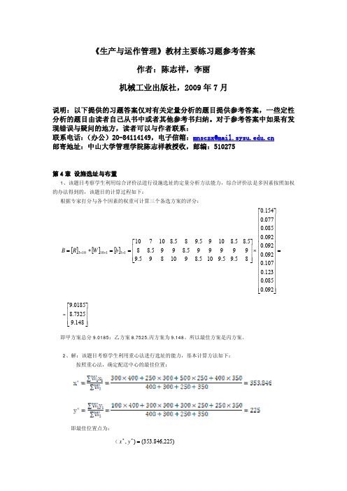
平衡后的生产线组合情况如下:
50 B 120 A
第 1 工作地
C 100 E I 30 20
40
第 5 工作地
第 3 工作地 F
80 D 60 J
60 H
第 2 工作地
第 6 工作地
G 90
第 4 工作地
按照节拍为 120 分钟的生产线平衡图 第 1 工作地为:{A} 第 2 工作地为:{B,H} 第 3 工作地为:{E,F} 第 4 工作地为:{G} 第 5 工作地为:{C,D} 第 6 工作地为:{I,J} (2)节拍为 150 分钟,计算最小工作地数:5。计算过程如下:
(2)计算节拍:
r=
Fe 8 × 60 − 30 = = 2.0045 ≈ 2 (分钟) N 220 /(10 − 2%)
(3)计算最小工作地数目:
⎡ ti S min = ⎢ ⎢ r ⎣
∑
⎤ ⎥ = ⎡ 0.4 + 1.5 + 1.0 + 0.4 + 0.6 + 0.9 + 0.4 + 0.4 + 0.6 + 0.7 + 1.0 + 0.4 ⎤ = [4.14] = 5 ⎥ 2.0045 ⎥ ⎢ ⎣ ⎦ ⎦
∑
工作地的组合如下: 第 1 工作地:{A} 第 2 工作地:{B,H} 第 3 工作地:{E,I} 第 4 工作地:{C,F,D} 第 5 工作地:{G,J} 平衡的结果图如下:
50 B 120
第 1 工作地
C 100 E
第 3 工作地
40
第 4 工作地
A 60
20 F
80
D 60 J
30
I G 90
ALPS编码器
Shaft Hollow Shaft Ring TypeDetector Slide Push Rotary Power Dual-in-linePackage TypeTACT SwitchTM■Typical SpecificationsRefer to P.167 for product specifications.Refer to P.167 for attached parts.Refer to P.168 for product varieties.Refer to P.193 for soldering conditions.Other varieties are also available. Please inquire.NoteShaft Hollow Shaft Ring TypeDetector Slide Push RotaryPower Dual-in-line Package Type TACT Switch TM11mm Size Metal Shaft TypeOther varieties are also available. Please inquire.NotePacking SpecificationsShaftHollow Shaft Ring TypeDetector SlidePush Rotary Power Dual-in-line Package Type TACT Switch TMShaft Hollow Shaft Ring TypeDetector Slide Push RotaryPower Dual-in-line Package Type TACT Switch TM11mm Size Metal Shaft TypeShaft Hollow Shaft Ring TypeDetectorSlide Push Rotary Power Dual-in-linePackage Type TACT Switch TMShaft Hollow Shaft Ring TypeDetector Slide Push RotaryPower Dual-in-line Package Type TACT Switch TMEC11EH 11mm Size Metal Shaft TypeShaft Hollow Shaft Ring TypeDetector Slide Push RotaryPowerDual-in-line Package TypeTACT Switch TMEC11B SeriesThe following parts are included with the product.Circuit DiagramShaft Hollow Shaft Ring TypeDetectorSlide Push RotaryPower Dual-in-line Package Type TACT Switch TM1. Single-shaft Type (EC11K is excluded. Refer to P.212 for EC11K )Shaft DimensionsUnit:mmDimensions marked with ( ) apply to products without push-on switches.1.Thehighlighted figures in shaft types refer to Product Specifications in P.161 and P.162. 2.Other varieties are also available. Please inquire.NotesShaft Hollow Shaft Ring TypeDetector Slide PushRotaryPower Dual-in-linePackage Type TACT Switch TM2. Standard Dimensions and configuration of Dual-shaft TypeUnit:mm1. The highlighted figures in shaft types refer to Product Specifications in P.1622. Other varieties are also available. Please inquire.NotesEncodersMetal Shaft Insulated ShaftHollowShaft Ring TypeDetector Slide Push Rotary Encoders Power Dual-in-line Package Type TACT Switch TMType Metal shaft9mm size 11mm size Series EC09EEC11BEC11EEC11GPhoto Output Incremental (Two phase A and B )Shaft types Single-shaftDual-shaft Single-shaftOperating direction VerticalHorizontalVerticalNumber of pulse / Number of detent15 / 309 / 1815 / 30 or Without 18 / 36 or Without15 / 30 or WithoutFeatures--Without detent Push-lock mechanism-Less shaft wobble Dimensions (mm )W 9.511.7D 13.812H4.55.54.58 / 8.5 4.5Operating temperature range–40℃ to +85℃Operating life 15,000 cycleAutomotive use ●●●●Life cycle (availability)ElectricalperformanceRating10mA 5V DC Max./min. operating current (Resistive load )10mA / 1mA Insulation resistance100M Ω min. 250V DCVoltage proof300V AC for 1 minuteor or 360V AC for 1s300V AC for 1 minute or 360V AC for 2sMechanical performanceRotational torque (Without detent )--7+ 3− 4mN ・m-8.5 ± 5 mN ・m Detent torque 8±5mN ・m12±7mN ・m10±7mN ・m12 ± 7 mN ・m Push-pull strength100NShaft configuration Flat Flat, Slotted, Serrated Inner-shaft :Flat Outer-shaft :SlottedSerratedTerminal typeInsertionSwitchSpecificationsSwitch type Push-on switchPush-lock mechanism switch ※Push-on switchContact arrangementSingle pole and single throw (Push-on )Travel (mm )0.5±0.31.5±0.50.5+ 0.4− 0.31.5±0.50.5±0.31.5±0.58±0.80.5±0.31.5±0.51.5±0.35Operating force (N )64±26±35±264±28 max.64±25±2Rating 10mA 5V DC 0.1A 5V DC(500μA 5V DC min. ratings )Contact resistance 100m Ω max. for initial period; 200m Ω max. after operating life.Operating life 10,000times min.25,000times min.20,000 times min.10,000times min.20,000 times min.Page160161● Encoders Soldering Conditions ・・・・・・・・・・・・・・・・・・・・・・・・・・・・・・・・・・・193● Encoders Cautions ・・・・・・・・・・・・・・・・・・・・・・・・・・・・・・・・・・・・・・・・194Notes1.※marked specification is only applicable to EC11E152U402.2. ●i ndicates applicability to all products in the series.+ 2.5− 2+ 2.5− 2+ 2.5− 2■ List of VarietiesEncodersMetal Shaft Insulated Shaft Hollow Shaft Ring TypeDetector Slide Push Rotary Encoders Power Dual-in-line Package Type TACT Switch TMType Metal shaft11mm size20mm sizeSeriesEC111EC11EHEC11KEC11JEC20A / RK203EM20BPhoto Output Self-return switchIncremental (Three phase A, B and C )Incremental (Two phase A and B )Shaft types Single-shaft Operating direction Vertical Number of pulse / Number of detent-6×ABC / 1810×ABC / 309 / 1815 / 3018 / 1840 / 40Features---Surface Mount Type-Magnetic type; LED indicator optionDimensions (mm )W 11.720.220D 131214.219.222.25H5 4.51013Operating temperature range–40℃ to +85℃–30℃ to +80℃–10℃ to +70℃Operating life 15,000 cycles30,000 cycles100,000 cycles 30,000 cycles500,000 rotationsAutomotive use ●●●●●-Life cycle (availability)Electrical performanceRating10mA 5V DC 1mA 5V DC 10mA 5V ±5% DC Max./min. operating current (Resistive load )10mA / 1mA -15mA / −Insulation resistance 100M Ω min. 250V DC10M Ω min. 50V DC 100M Ω min. 250V DC Voltage proof300V AC for 1 minute or 360V AC for 2s 300V AC for 1 minute or 360V AC for 1s50V AC for 1 minute or 60V AC for 2s 300V AC for 1 minute or 360V AC for 2s Mechanical performanceRotational torque (Without detent )3 to 30mN ・m -7mN ・m max.Detent torque -10±7mN ・m12±5mN ・m40±20mN ・m8±5mN ・m Push-pull strength100NShaft configuration Flat, Slotted, Serrated FlatTerminal typeInsertionReflowInsertionSwitchSpecificationsSwitch type Push-on switch Contact arrangement Single pole and single throw (Push-on )Travel (mm )0.5±0.3 1.5±0.50.5±0.3 1.5±0.50.5±0.3 1.5±0.50.5±0.31.5±0.50.5Operating force (N )6 4±264±25±24±25±24±26±3Rating 0.1A 5V DC(500μA 5V DC min. ratings )0.1A 5V DC(0.1mA 5V DC min. ratings )0.5A 16V DC(1mA 16V DC min. ratings )0.1A 5V DCContact resistance 100m Ω max. for initial period; 200m Ω max. after operating life.Operating life 20,000 times min.1,000,000 times min.100,000 times min.1,000,000 times min.100,000 times min.20,000 times min.25,000 times min.Page161170172● Encoders Soldering Conditions ・・・・・・・・・・・・・・・・・・・・・・・・・・・・・・・・・・・193● Encoders Cautions ・・・・・・・・・・・・・・・・・・・・・・・・・・・・・・・・・・・・・・・・194Note ●i ndicates applicability to all products in the series.+ 2.5− 2+ 2.5− 2+ 0.4− 0.3■ List of VarietiesDetector SlidePushRotary PowerDual-in-line Package Type TACT Switch TMCondition for Reflow Reference for Hand SolderingTemperature profile1.When using an infrared reflow oven, solder may sometimes not be applied. Be sure to use a hot air reflow oven or a type that uses infrared rays in combination with hot air.2.The temperatures given above are the maximum temperatures at the terminals of the potentiometer when employing a hot air reflow method. The temperature of the PC board and the surface temperature of the potentiometer may vary greatly depending on the PC board material, its size and thickness. Ensure that the surface temperature of the potentiometer does not rise to 250°C or greater.3.Conditions vary to some extent depending on the type of reflow bath used. Be sure to give due consideration to this prior to use.Notes300200100RoomT e m p e r a t u r e (˚C )。
SJ-05设计开发方案
g.阀杆在全开和全关状态下有最高和最低位置限限制,实现阀门在全开、全关位置锁定,起安全保险作用;
h.阀门设计有排污和泄压结构,安装泄压装置,也可起到泄压作用。
2、设计路线
依据用户要求和有关技术标准等设计输入文件,首先进行产品方案设计,然后进行工程设计,进行设计计算,绘制产品图纸,编排工艺,编制产品使用说明书等设计输出文件,设计输出文件经评审通过后签发到有关部门,各部门依据图纸和工艺生产5台样机,通过对样机的生产和测试进行设计验证,期间可能有设计不合理的地方要进行设计更改。验证合格后,由市场部与用户联系,委托用户在相应工况下使用该阀门,进行设计确认。
③结构设计:
a.本产品采用法兰与管道连接;用手轮手动来控制阀门的开启和关闭动作;
b.阀体中法兰与阀盖密封,采用金属复合垫片;
c.阀盖填料孔内,填料材料用柔性石墨及隔环加注密封油脂,密封性能可靠;
d.闸板平行密封面渡镍磷,阀座密封面材料为PTFE,软硬密封面性能可靠;
e.主要零部件:阀体、阀盖、平闸板、阀杆、阀座、手轮等组成;
备注:
编制
时间
审批
时间
气密封试验
0.6
空气
120
零泄漏
设计原理及路线概述(可另加页叙述):
1、设计原理
①工作原理:通过手轮在阀杆上端施加一定的转矩,通过阀杆传递给闸板,使之沿阀杆轴线上下移动,实现全开或全闭动作。
②密封机理:闸阀平板自由紧贴在PTFE阀座上,在流体压力作用下,平板在流体流动方向上产生位移,使之与阀座密封面更紧密的接触,比压增大形成密封,由于阀座为非下平板压向阀座,实现金属平闸板与非金属阀座密封。
电池型号对应表
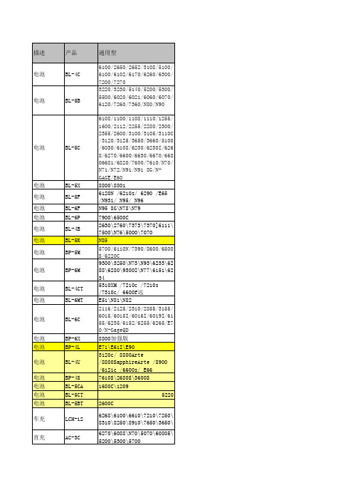
车载充电器 D828车充
车载充电器 G608车充
车载充电器 W579车充
类别:默认分类 | 评论(0) | 浏览(142 ) 浦诺菲手机配件通用型一览表3
2009年06月14日 星期日 下午 01:39
产品 通用性 描述
电池 电池 电池 电池 电池 电池 电池 电池 充电器
565/575/58 565/575/585/586/566 5 586/566 818/828+ 818/828+ 838/D600 D600/E806C S700/S505 P800/D802 515/535/68 6 565/575/585/586/566 818/828+/830 818/828+/830 838/D600 D600/E806C S700/S505 P800/D802 515/535/686
描述
产品
通用型 6100/2650/2652/3108/5100/ 6100/6102/6170/6260/6300/ 7200/7270 3220/3230/5140/5200/5300/ 5500/6020/6021/6060/6070/ 6120/7260/7360/N80/N90 6108/1100/1108/1110/1255/ 1600/2112/2255/2280/2300/ 2355/2600/3100/3105/3110C /3120/3125/3650/3660/5100 /6030/6108/6230/6230I/626 8/6270/6600/6630/6670/668 06681/6820/7600/7610/N70/ N71/N72/N91/N91 8G/NGAGE/E60 8800\8801 6120N /6210s/ 6290 /E65 /N93i/ N95/ N96 N95 8G\N78\N79 7900\6500C 2630\2760\7373\7370]6111\ 7500\N76\5000\7070 N85 5700/6110N/7390/8600/6500 S/6220C 9300\3250\N73\N93\6233\62 88\6280\9300I\N77\6151\62 34 5310XM /7210c /7210s /7310c/ 6600f远 E51\N81\N82 2116/2125/2310/2855/3155/ 6015/6015I/6016I/6019I/61 55/6235/6152/6255/6265/E7 0/N-GageQD 8800加强版 E71\E61I\E90 3120c/ 8800Arte /8800SapphireArte /8900 /6121c /6600s/ E66 7610S\2680S\3600S 1680C\1209 5220 2600C 6268\6100\6610\7210\7250\ 8310\8250\8910\7650\3650\ 6270\6088\N70\5070\60805\ 5200\5300\5700
- 1、下载文档前请自行甄别文档内容的完整性,平台不提供额外的编辑、内容补充、找答案等附加服务。
- 2、"仅部分预览"的文档,不可在线预览部分如存在完整性等问题,可反馈申请退款(可完整预览的文档不适用该条件!)。
- 3、如文档侵犯您的权益,请联系客服反馈,我们会尽快为您处理(人工客服工作时间:9:00-18:30)。
两者互为构象异构体
5.4 环烷烃的结构
椅型构象
稳定(99.9%以上) C-C-C键角基本保持109.5° 任何两个相邻的C-H键都是交叉式的 椅型构象无张力环
H
3 H 2 H 5 6 H 4
H
H
1
H H H 3 H
5 4 2
H
1 6
H H
H C4-C3
H
H H
H
H
H
透视式
C6-C1
纽曼投影式
25
张力越大,稳定性越低
19
5.4 环烷烃的结构
角变化
5.4.1 环丙烷的结构 σ 键轨道的交盖
104 o H C H
交盖较好
交盖较差
H H
C
C H
H
C-C键的电子云没有轨道轴对称,而是分布 在一条曲线上,故常称弯曲键 弯曲键比一般的 σ 键弱,且具有较高的能量 角张力——环的键角偏离正常sp3键角而引 起的张力 扭转张力——重叠式构象而引起的张力 20
10
5.2 脂环烃的性质
物理性质:沸点,熔点,密度 化学性质(1与脂肪烃类似,2环状结构的特性)
环烷烃的反应(取代,开环,氧化) 环烯烃和环二烯烃的反应(加成,氧化,双烯合成)
11
5.2 脂环烃的性质
5.2.1 环烷烃的反应
五元以上 环烷烃 性质相似 链状烷烃
环 的 大 小 与 化 学 性 质
5.3进行解释
5.4 环烷烃的结构
5.4.2 环丁烷的结构 若为平面型分子
C4-C3
H
4
3
H HH
H H
4
3
2 1
HH
HH
C1-C2
1
2
H
H
H H
H H
重叠式构象
88o
实际为折叠式构象(稳定)
H H H
4
H
32
H
2
3
H
1
4
2
H H
1
H2C H2C
3
H
14
H
H H
21
C1-C2
角张力稍增加, 扭转张力明显减小
5.4 环烷烃的结构
17
5.2 脂环烃的性质
双烯合成
+
COOCH3
H COOCH3
双环[2.2.1]-5-庚烯-2-羧酸甲酯
+
CH CH
双环[2.2.1]-2,5-庚二烯
18
5.3 环烷烃的环张力和稳定性
烷烃:每增加一个 CH2 , 燃烧热 增值基本 一定,平均为658.6 kJ/mol. 环烷烃:平均每个 CH2 的燃烧热为ΔHc/n. 如:环丙烷的 ΔHc/n 为697.1 kJ/mol 张力能——环丙烷的的平均每个 CH2的燃 烧热烷烃高38.5 kJ/mol.这个差值就 是环丙烷分子中每个 CH2的张力能. 总 张 力 能 —— 环 丙 烷 的 总 张 力 能 38.5×3=115.5 kJ/mol 比较环烷烃的稳定性
HNO3
热
HOOC COOH
16
5.2 脂环烃的性质
5.2.2 环烯烃和环二烯烃的反应 加成反应(不开环)
+ Br2
CCl 4
H Br
Br H
CH3 I
CH3 + HI
氧化反应(开环)
O3
Zn, H2O
CH 2 CH 2 CHO CH 2 CH 2 CHO
KMnO4
CH 3 CHCH 2COOH CH 2CH 2COOH
29
5.4 环烷烃的结构
甲基环己烷椅型构象的翻转
两种椅型构象是两种不同结构的分子 甲基连在a键上的构象具有较高的能量,较不稳定 平衡体系中e键甲基环己烷占95%,a键的占5%
30
5.4 环烷烃的结构
取代基在e键上的构象较稳定
若环上有多个取代基,往往是 e 键取代基最多的构象最稳定 若环上有不同取代基,则体积大的取代基连在 e键上的构象最稳定 例: 1,2-二甲基环己烷,顺反式如下: 同一平面上的比较 在同侧为顺:a,e 在异侧为反:a,a;e,e 反式(e,e)比顺式(a,e)的稳定 (a,a)实际上不存在(能量太高)
环烷烃 环丙烷 环丁烷 环戊烷 环己烷 环庚烷 环辛烷 环壬烷 环癸烷 环十五烷 烷烃 ΔHc/n 总张力能 (kJ/mol) (kJ/mol) 697.1 686.2 664.0 658.6 662.3 663.6 664.4 663.6 658.6 658.6 115.5 110.4 27.0 0 25.9 40.0 52.2 50.0 0 -
螺原子
2 3 4 10 9 1 6 5 7 8
3 2 7 6 1 4 5
螺[4. 5]癸烷
spiro[4. 5]decane
4−甲基螺[2. 4]庚烷
4−methylspiro[2. 4]heptane
8
5.1 脂环烃的分类和命名
桥环烃(Bridged hydrocarbon)的命名
桥环烃——脂环烃分子中两个碳环共用二个及以上碳原子 根据成环碳原子总数称为双环某烷; 编号从一个桥头碳开始,按从大到小编各桥;编号顺序以取 代基的位置和最小为原则。 将各桥的碳原子数从大到小写在方括号里,用圆点分开。 注意:桥头碳原子数不包括桥头碳
3
H
2 5
H 1 H
6
H H
H H
4 3 2
1 5
6
HH
H C5-C6
H H
H H
H H 重叠式 (有扭转张力)
26
H H
5.4 环烷烃的结构
椅型和船型构象的C-H键
2.50Å 1.84Å
H H H H H H H H H
H
H H
H
H H H H
H
2.27Å
H
H
2.49Å
H
H H
2.27Å
2.49Å
构型异构体 (顺反) 条件:环上只要有两个C各连有不同取代基时
CH3 CH3
CH3 H
H
H
H
CH3
顺反异构用“顺” 或“反”注明基团 相对位置。 英文 用 “cis”和“trans” 表示。
6
顺-1,4-二甲基环己烷
反-1,4-二甲基环己烷
5.1 脂环烃的分类和命名
不饱和脂环烃的命名 (环烯烃,环炔烃,环二烯烃等)
5
二环[2. 2. 1]庚烷 bicyclo[2. 2. 1]heptane
2, 7, 7−三甲基二环[2. 2. 1]庚烷 2, 7, 7−trimethylbicyclo[2. 2. 1]heptane
9
2 1 3 4 5
8 7 6
8−甲基二环[4. 3. 0]壬烷 8−methylbicyclo[4. 3. 0]nonane
以环为母体,名称 用“环” (英文用 “cyclo”)开头。 环外基团作为环上 的取代基
环丙烷
环己烷
甲基环丙烷
cyclopropane cyclohexane methylcyclopropane
1 2 3 4 1 2 3
取代基位置数字取 最小
CH3
1, 3-二甲基环己烷 1, 3−dimethyl− cyclohexane
桥头碳原子
10 9 8 7 1 2 3 4 5
桥头间的碳原子数 (用"."隔开) 环的数目 二环[4. 4. 0]癸烷 bicyclo[4. 4. 0]decane
9
组成桥环的 碳原子总数
6
十氢萘
5.1 脂环烃的分类和命名
桥环烃(Bridged hydrocarbon)的命名
7 1 6 4 3 2 5 6 2 4 3 7 1
螺环烃(Spiro hydrocarbon)的命名
螺环烃——脂环烃分子中两个碳环共有一个碳原子 根据成环碳原子的总数称为螺某烷; 编号以较小环中与螺原子相邻C开始,经过螺原子再编第二个环; 取代基编号最小; 螺字后 方括号 用数字标出两个碳环上除了共有碳原子外的碳原子 数目,小的数字排前面;数字用圆点隔开,代表碳原子数。
Cl2 / hv
Cl
自由基取代反应
H2 / Pt 催化加氢
HI
不反应 不容易发生
不反应
!!!
小环环烷烃 活泼,易开环
12
5.2 脂环烃的性质
小环环烷烃的开环反应(即加成反应)
小环化合物的催化加氢
+
+
+
H2
H2
H2
Ni
80℃
Ni
CH 3 CH 2 CH 3
CH 3 CH 2 CH 2 CH 3
CH 3 CH 2 CH 2 CH 2 CH 3
5.4.3 环戊烷的结构
不是平面结构:平面的C-H键的重叠,有较大扭转张力 实际构象:折叠环的形式——“信封式”构象
分子张力不大,因此环戊烷的化学性质比较稳定
22
5.4 环烷烃的结构
5.4.4 环己烷的结构与构象 环己烷不是平面型分子
如果环己烷的 6 个碳原子在同一平面上: 将有角张力 将有扭转张力
第五章 脂环烃 (Cyclic Aliphatic)
§5.1 §5.2 §5.3 §5.4 §5.5 脂环烃的分类和命名 脂环烃的性质 环烷烃的环张力和稳定性 环烷烃的结构 萜类和甾族化合物 (自学)
1
重点
重点
作 业
P109: 1,5(135),6,9
2
5.1 脂环烃的分类和命名
脂环烃——碳骨架为环状,性质与开链烃相似的烃类。
3 2
环的断裂:含氢 最多和最少的C-C上 马氏加成:反应 选择性与碳正离子稳