M74HC238M1R中文资料
74HC系列芯片介绍
74HC00 四2输入端与非门TI[DATA]74HC01 四2输入端与非门(OC)74HC02 四2输入端或非门TI[DATA]74HC03 四2输入端与非门(OC) TI[DATA]74HC04 六反相器TI[DATA]74HC05 HEX INVERTERS74HC08 四2输入端与门TI[DATA]74HC09 QUADRUPLE 2-INPUT POSITIVE-AND74HC10 三3输入端与非门TI[DATA]74HC11 三3输入端与门TI[DATA]74HC14 双4输入端与非门TI[DATA]74HC20 双4输入端与非门TI[DATA]74HC21 双4输入端与门TI[DATA]74HC27 三3输入端或非门TI[DATA]74HC30 8输入端与非门TI[DATA]74HC32 四2输入端或门TI[DATA]74HC42 4线-10线译码器(BCD输入) TI[DATA]74HC73 DUAL J-K FLIP-FLOP TI[DATA]74HC74 双上升沿D型触发器TI[DATA]74HC75 4-BIT BISTABLE LATCH TI[DATA]74HC85A 四位数值比较器TI[DATA]74HC86 四2输入端异或门TI[DATA]74HC93 双4输入端与非门TI[DATA]74HC107 双主-从J-K触发器TI[DATA]74HC109 双J-K触发器TI[DATA]74HC112 双下降沿J-K触发器TI[DATA]74HC123 可重触发双稳态触发器TI[DATA]74HC125 四总线缓冲器TI[DATA]74HC126 四总线缓冲器74HC132 四2输入端与非门74HC133 13-INPUT POSITIVE-NAND74HC137 地址锁存3线-8线译码器74HC138 3线-8线译码器74HC139 双2线-4线译码器74HC147 10线-4线优先编码器74HC148 8-LINE TO 3-LINE PRIORITY ENCODERS 74HC151 8-INPUT MULTIPLEXER74HC153 DUAL 4-INPUT MULTIPLEXER74HC154 4线-16线译码器74HC157 四2选1数据选择器74HC158 四2选1数据选择器74HC160 DECADE COUNTER74HC161 4位二进制同步计数器74HC162 DECADE COUNTER74HC163 4-BIT BINARY PRESETTABLE COUNTER74HC164 8位移位寄存器74HC165 8位并行输入/串行输出寄存器74HC166 8位并行输入/串行输出移位寄存器TI,PHI74HC173 4位D型寄存器TI74HC174 HEX D-TYPE FLIP-FLOP WITH RESET TI 74HC175 四上升沿D型触发器TI74HC190 十进制同步加/减计数器TI74HC191 4位二进制同步加/减计数器TI74HC192 BCD二进制同步加/减计数器TI74HC193 可预置4位二进制加/减计数器TI74HC194 4位并入/串入-并出/串出移位寄存TI74HC195 4位移位寄存器TI74HC221 双单稳态触器TI74HC237 3-8线译码器(带地址锁存)TI74HC238 3-8线译码器TI74HC239 双2-4线译码器74HC240 八反相缓冲/线驱动/线接收器TI74HC241 八缓冲/线驱动/线接收器TI74HC243 四总线收发器TI74HC244 八缓冲/线驱动/线接收器TI,FSC74HC245 八双向总线发送/接发器TI,FSC74HC251 8选1数据选择器74HC253 双4选1数据选择器74HC257 四2选1数据选择器74HC258 四2选1数据选择器74HC259 8位可寻址锁存器74HC266 QUADRUPLE 2-INPUT EXCLUSIVE-NOR74HC273 八D触发器74HC280 9位奇偶产生器/校验器TI74HC283 4位二进制超位全加器74HC297 DIGITAL PHASE-LOCKED-LOOP74HC299 8位双向通用移位/存储寄存器74HC354 带锁存三态8-1多路转换开关74HC365 六总线驱动器74HC366 六反相总线驱动器74HC367 六总线驱动器74HC368 六反相总线驱动器74HC373 六D型锁存器74HC374 六上升沿D型触发器74HC375 4-BIT BISTABLE LATCH74HC377 六上升沿D型触发器74HC378 6-BIT D-TYPE FLIP-FLOP74HC379 QUADRUPLE D-TYPE FLIP-FLOP74HC390 双十进制计数器74HC393 双4位二进制计数器74HC4002 高速CMOS双4输入端或非门74HC4015 高速CMOS双4位串入/并出移位寄存器74HC4016 高速CMOS四传输门74HC4017 高速CMOS十进制计数/分配器74HC4020 高速CMOS14级串行二进制计数/分频器74HC4024 高速CMOS7级二进制串行计数/分频器74HC4040 高速CMOS12级二进制串行计数/分频器74HC4046A 高速CMOS锁相环74HC4049 高速CMOS六反相缓冲/变换器74HC4050 高速CMOS六同相缓冲/变换器74HC4051 高速CMOS八选一模拟开关74HC4052 高速CMOS双4选1模拟开关74HC4053 高速CMOS三组二路模拟开关74HC4059 高速CMOS“N”分频计数器74HC4060 高速CMOS14级二进制串行计数/分频器74HC4061 14-STAGE BINARY COUNTER/OSCILLATOR 74HC4066 高速CMOS四传输门74HC4067 高速CMOS16选1模拟开关74HC4075 高速CMOS三3输入端或门74HC4078A 8-INPUT OR/NOR74HC4094 高速CMOS8位移位存储总线寄存器74HC40103 高速CMOS8位可预置同步二进制减法计数器74HC40105 高速CMOS先入先出FI-FD寄存器74HC423 双单稳态振荡器TI[DATA]74HC4316 高速CMOS四模拟开关TI74HC4351 ANALOG MULTIPLEXER/DEMULTIPLEXER TI 74HC4352 ANALOG MULTIPLEXER/DEMULTIPLEXER TI 74HC4511 高速CMOSBCD锁存,7段译码,驱动器74HC4514 高速CMOS4位锁存,4线-16线译码器74HC4515 高速CMOS4位锁存,4线-16线译码器74HC4518 高速CMOS双BCD同步加计数器74HC4520 高速CMOS双4位二进制同步加计数器74HC4538 高速CMOS精密双单稳TI,INT(HAR)74HC4543 高速CMOSBCD七段锁存译码,驱动器74HC4724 8-BIT ADDRESSABLE LATCHES74HC533 三态八D锁存器74HC534 三态八D锁存器74HC540 八路三态收发缓冲器(反相)74HC541 八路三态收发缓冲器(同相)74HC563 三态八D锁存器74HC564 三态八D锁存器74HC573 四3选1数据选择器74HC574 双4选1数据选择器74HC590A 8位二进制计数器TI74HC594 8位移位寄存器TI74HC595 8位移位三态寄存器TI,ST[DATA],FSC,PHI74HC597 8位移位寄存器74HC623 OCTAL BUS TRANSCEIVER TI74HC640 OCTAL BUS TRANSCEIVER74HC643 OCTAL BUS TRANSCEIVER TI74HC645 OCTAL BUS TRANSCEIVER TI74HC646 OCTAL BUS TRANSCEIVER/REGISTER74HC648 OCTAL BUS TRANSCEIVER/REGISTER TI 74HC651 OCTAL BUS TRANSCEIVER/REGISTER TI 74HC652 OCTAL BUS TRANSCEIVER/REGISTER TI 74HC664 OCTAL BUS TRANSCEIVER TI74HC665 OCTAL BUS TRANSCEIVER TI74HC670 4-BY-4 REGISTER FILE74HC682 8-BIT MAGNITUDE COMPARATORS74HC684 8-BIT MAGNITUDE COMPARATORS TI74HC688 8-BIT MAGNITUDE COMPARATOR74HC7001 QUADRUPLE POSITIVE-AND TI74HC7002 QUADRUPLE POSITIVE-NOR TI74HC7032 QUADRUPLE POSITIVE-OR TI74HC7074 6-SECTION MULTIFUNCTION CIRCUIT TI 74HC7046A 压控锁相环74HC7266 QUAD 2-INPUT EXCLUSIVE-NOR GATE 74HCU04 HEX INVERTER TI。
74HC138中文资料
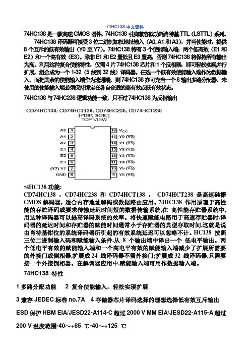
74HC138中文资料74H C138是一款高速C MOS器件,74H C138引脚兼容低功耗肖特基TTL(LS TTL)系列。
74HC138译码器可接受3位二进制加权地址输入(A0, A1和A3),并当使能时,提供8个互斥的低有效输出(Y0至Y7)。
74H C138特有3个使能输入端:两个低有效(E1和E2)和一个高有效(E3)。
除非E1和E2置低且E3置高,否则74H C138将保持所有输出为高。
利用这种复合使能特性,仅需4片74H C138芯片和1个反相器,即可轻松实现并行扩展,组合成为一个1-32(5线到32线)译码器。
任选一个低有效使能输入端作为数据输入,而把其余的使能输入端作为选通端,则74H C138亦可充当一个8输出多路分配器,未使用的使能输入端必须保持绑定在各自合适的高有效或低有效状态。
74H C138与74H C238逻辑功能一致,只不过74HC138为反相输出74HC138功能:CD74HC138 ,CD74HC238和CD74HCT138 ,CD74HCT238是高速硅栅CMOS解码器,适合内存地址解码或数据路由应用。
74HC138 作用原理于高性能的存贮译码或要求传输延迟时间短的数据传输系统,在高性能存贮器系统中,用这种译码器可以提高译码系统的效率。
将快速赋能电路用于高速存贮器时,译码器的延迟时间和存贮器的赋能时间通常小于存贮器的典型存取时间,这就是说由肖特基钳位的系统译码器所引起的有效系统延迟可以忽略不计。
HC138 按照三位二进制输入码和赋能输入条件,从8 个输出端中译出一个低电平输出。
两个低电平有效的赋能输入端和一个高电平有效的赋能输入端减少了扩展所需要的外接门或倒相器,扩展成24 线译码器不需外接门;扩展成32 线译码器,只需要接一个外接倒相器。
在解调器应用中,赋能输入端可用作数据输入端。
74HC138 特性1多路分配功能 2 复合使能输入,轻松实现扩展3兼容JEDEC标准no.7A 4存储器芯片译码选择的理想选择低有效互斥输出ESD保护HBM EIA/JESD22-A114-C超过2000 V MM EIA/JESD22-A115-A超过200 V温度范围-40~+85 ℃-40~+125 ℃74HC245简介:总线驱动器,典型的TTL型三态缓冲门电路。
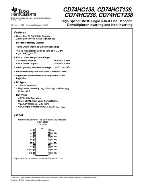
M74HC238高速CMOS3到8线解码器数据手册说明书

1/10July 2001sHIGH SPEED:t PD = 15ns (TYP .) at V CC = 6V sLOW POWER DISSIPATION:I CC = 4µA(MAX.) at T A =25°C sHIGH NOISE IMMUNITY:V NIH = V NIL = 28 % V CC (MIN.)sSYMMETRICAL OUTPUT IMPEDANCE:|I OH | = I OL = 4mA (MIN)sBALANCED PROPAGATION DELAYS:t PLH ≅ t PHLsWIDE OPERATING VOLTAGE RANGE:V CC (OPR) = 2V to 6VsPIN AND FUNCTION COMPATIBLE WITH 74 SERIES 238DESCRIPTIONThe M74HC238 is an high speed CMOS 3 TO 8LINE DECODER fabricated with silicon gate C 2MOS technology.If the device is enabled, 3 binary select inputs (A,B and C) determine which one of outputs will go high. When enable input G1 is held "Low" or either G2A or G2B is held "High" decoding function isinhibited and all the 8 outputs go low. Three enable inputs are provided to ease cascade connection and application of this address decoder in memory systems.All inputs are equipped with protection circuits against static discharge and transient excess voltage.M74HC2383 TO 8 LINE DECODERPIN CONNECTION AND IEC LOGIC SYMBOLSORDER CODESPACKAGE TUBE T & RDIP M74HC238B1R SOP M74HC238M1RM74HC238RM13TR TSSOPM74HC238TTRM74HC2382/10INPUT AND OUTPUT EQUIVALENT CIRCUITPIN DESCRIPTIONTRUTH TABLEX : Don’t CareLOGIC DIAGRAMPIN No SYMBOL NAME AND FUNCTION 1, 2, 3A, B, C Data Inputs4, 5 G2A G2B Enable Input (Active LOW)6G1Data Enable Input (Active HIGH)15, 14, 13, 12, 11, 10, 9,7Y0 to Y7Outputs8GND Ground (0V)16V CCPositive Supply VoltageINPUTSOUTPUTS SELECTED OUTPUTENABLE SELECTG2B G2A G1C B A Y0Y1Y2Y3Y4Y5Y6Y7X X L X X X L L L L L L L L NONE X H X X X X L L L L L L L L NONE H X X X X X L L L L L L L L NONE L L H L L L H L L L L L L L Y0L L H L L H L H L L L L L L Y1L L H L H L L L H L L L L L Y2L L H L H H L L L H L L L L Y3L L H H L L L L L L H L L L Y4L L H H L H L L L L L H L L Y5L L H H H L L L L L L L H L Y6LLHHHHLLLLLLLHY7M74HC2383/10ABSOLUTE MAXIMUM RATINGSAbsolute Maximum Ratings are those values beyond which damage to the device may occur. Functional operation under these conditions is not implied(*) 500mW at 65 °C; derate to 300mW by 10mW/°C from 65°C to 85°CRECOMMENDED OPERATING CONDITIONSSymbol ParameterValue Unit V CC Supply Voltage -0.5 to +7V V I DC Input Voltage -0.5 to V CC + 0.5V V O DC Output Voltage -0.5 to V CC + 0.5V I IK DC Input Diode Current ± 20mA I OK DC Output Diode Current ± 20mA I O DC Output Current ± 25mA I CC or I GND DC V CC or Ground Current± 50mA P D Power Dissipation 500(*)mW T stg Storage Temperature -65 to +150°C T LLead Temperature (10 sec)300°CSymbol ParameterValue Unit V CC Supply Voltage 2 to 6V V I Input Voltage 0 to V CC V V O Output Voltage 0 to V CC V T op Operating Temperature -55 to 125°C t r , t fInput Rise and Fall TimeV CC = 2.0V 0 to 1000ns V CC = 4.5V 0 to 500ns V CC = 6.0V0 to 400nsM74HC2384/10DC SPECIFICATIONSAC ELECTRICAL CHARACTERISTICS (C L = 50 pF, Input t r = t f = 6ns)SymbolParameterTest ConditionsValue UnitV CC (V)T A = 25°C -40 to 85°C -55 to 125°C Min.Typ.Max.Min.Max.Min.Max.V IHHigh Level Input Voltage2.0 1.5 1.5 1.5V 4.53.15 3.15 3.156.04.24.24.2V ILLow Level Input Voltage2.00.50.50.5V4.5 1.35 1.35 1.356.0 1.81.81.8V OHHigh Level Output Voltage2.0I O =-20 µA 1.9 2.0 1.9 1.9V4.5I O =-20 µA 4.4 4.5 4.4 4.46.0I O =-20 µA5.96.0 5.9 5.94.5I O =-4.0 mA 4.18 4.31 4.13 4.106.0I O =-5.2 mA 5.685.8 5.635.60V OLLow Level Output Voltage2.0I O =20 µA 0.00.10.10.1V 4.5I O =20 µA 0.00.10.10.16.0I O =20 µA 0.00.10.10.14.5I O =4.0 mA 0.170.260.330.406.0I O =5.2 mA 0.180.260.330.40I I Input Leakage Current6.0V I = V CC or GND ± 0.1± 1± 1µA I CCQuiescent Supply Current6.0V I = V CC or GND44080µA SymbolParameterTest ConditionsValue UnitV CC (V)T A = 25°C -40 to 85°C -55 to 125°C Min.Typ.Max.Min.Max.Min.Max.t TLH t THL Output TransitionTime 2.0307595110ns 4.581519226.07131619t PLH t PHL Propagation DelayTime (A, B, C - Y) 2.050150190225ns4.5173038456.015263238t PLH t PHL Propagation DelayTime (G1 - Y) 2.050150190225ns4.5173038456.015263238t PLH t PHL Propagation DelayTime (G2 - Y)2.050150190225ns4.5173038456.015263238M74HC2385/10CAPACITIVE CHARACTERISTICS1) C PD is defined as the value of the IC’s internal equivalent capacitance which is calculated from the operating current consumption without load. (Refer to Test Circuit). Average operating current can be obtained by the following equation. I CC(opr) = C PD x V CC x f IN + I CCTEST CIRCUITL R T = Z OUT of pulse generator (typically 50Ω)SymbolParameterTest ConditionsValue UnitV CC (V)T A = 25°C -40 to 85°C -55 to 125°C Min.Typ.Max.Min.Max.Min.Max.C IN Input Capacitance 5.05101010pF C PDPower Dissipation Capacitance (note 1)5.053pFM74HC2386/10WAVEFORM 1: PROPAGATION DELAY TIMES(f=1MHz; 50% duty cycle)M74HC238Information furnished is believed to be accurate and reliable. However, STMicroelectronics assumes no responsibility for the consequences of use of such information nor for any infringement of patents or other rights of third parties which may result from its use. No license is granted by implication or otherwise under any patent or patent rights of STMicroelectronics. Specifications mentioned in this publication are subject to change without notice. This publication supersedes and replaces all information previously supplied. STMicroelectronics products are not authorized for use as critical components in life support devices or systems without express written approval of STMicroelectronics.© The ST logo is a registered trademark of STMicroelectronics© 2001 STMicroelectronics - Printed in Italy - All Rights ReservedSTMicroelectronics GROUP OF COMPANIESAustralia - Brazil - China - Finland - France - Germany - Hong Kong - India - Italy - Japan - Malaysia - Malta - MoroccoSingapore - Spain - Sweden - Switzerland - United Kingdom© 10/10。
74系列芯片功能大全
74系列芯片功能大全7400 TTL 2输入端四与非门7401 TTL 集电极开路2输入端四与非门7402 TTL 2输入端四或非门7403 TTL 集电极开路2输入端四与非门7404 TTL 六反相器7405 TTL 集电极开路六反相器7406 TTL 集电极开路六反相高压驱动器7407 TTL 集电极开路六正相高压驱动器7408 TTL 2输入端四与门7409 TTL 集电极开路2输入端四与门7410 TTL 3输入端3与非门74107 TTL 带清除主从双J-K触发器74109 TTL 带预置清除正触发双J-K触发器7411 TTL 3输入端3与门74112 TTL 带预置清除负触发双J-K触发器7412 TTL 开路输出3输入端三与非门74121 TTL 单稳态多谐振荡器74122 TTL 可再触发单稳态多谐振荡器74123 TTL 双可再触发单稳态多谐振荡器74125 TTL 三态输出高有效四总线缓冲门74126 TTL 三态输出低有效四总线缓冲门7413 TTL 4输入端双与非施密特触发器74132 TTL 2输入端四与非施密特触发器74133 TTL 13输入端与非门74136 TTL 四异或门74138 TTL 3-8线译码器/复工器74139 TTL 双2-4线译码器/复工器7414 TTL 六反相施密特触发器74145 TTL BCD—十进制译码/驱动器7415 TTL 开路输出3输入端三与门74150 TTL 16选1数据选择/多路开关74151 TTL 8选1数据选择器74153 TTL 双4选1数据选择器74154 TTL 4线—16线译码器74155 TTL 图腾柱输出译码器/分配器74156 TTL 开路输出译码器/分配器74157 TTL 同相输出四2选1数据选择器74158 TTL 反相输出四2选1数据选择器7416 TTL 开路输出六反相缓冲/驱动器74160 TTL 可预置BCD异步清除计数器74161 TTL 可予制四位二进制异步清除计数器74162 TTL 可预置BCD同步清除计数器74163 TTL 可予制四位二进制同步清除计数器74164 TTL 八位串行入/并行输出移位寄存器74165 TTL 八位并行入/串行输出移位寄存器74166 TTL 八位并入/串出移位寄存器74169 TTL 二进制四位加/减同步计数器7417 TTL 开路输出六同相缓冲/驱动器74170 TTL 开路输出4×4寄存器堆74173 TTL 三态输出四位D型寄存器74174 TTL 带公共时钟和复位六D触发器74175 TTL 带公共时钟和复位四D触发器74180 TTL 9位奇数/偶数发生器/校验器74181 TTL 算术逻辑单元/函数发生器74185 TTL 二进制—BCD代码转换器74190 TTL BCD同步加/减计数器74191 TTL 二进制同步可逆计数器74192 TTL 可预置BCD双时钟可逆计数器74193 TTL 可预置四位二进制双时钟可逆计数器74194 TTL 四位双向通用移位寄存器74195 TTL 四位并行通道移位寄存器74196 TTL 十进制/二-十进制可预置计数锁存器74197 TTL 二进制可预置锁存器/计数器7420 TTL 4输入端双与非门7421 TTL 4输入端双与门7422 TTL 开路输出4输入端双与非门74221 TTL 双/单稳态多谐振荡器74240 TTL 八反相三态缓冲器/线驱动器74241 TTL 八同相三态缓冲器/线驱动器74243 TTL 四同相三态总线收发器74244 TTL 八同相三态缓冲器/线驱动器74245 TTL 八同相三态总线收发器74247 TTL BCD—7段15V输出译码/驱动器74248 TTL BCD—7段译码/升压输出驱动器74249 TTL BCD—7段译码/开路输出驱动器74251 TTL 三态输出8选1数据选择器/复工器74253 TTL 三态输出双4选1数据选择器/复工器74256 TTL 双四位可寻址锁存器74257 TTL 三态原码四2选1数据选择器/复工器74258 TTL 三态反码四2选1数据选择器/复工器74259 TTL 八位可寻址锁存器/3-8线译码器7426 TTL 2输入端高压接口四与非门74260 TTL 5输入端双或非门74266 TTL 2输入端四异或非门7427 TTL 3输入端三或非门74273 TTL 带公共时钟复位八D触发器74279 TTL 四图腾柱输出S-R锁存器7428 TTL 2输入端四或非门缓冲器74283 TTL 4位二进制全加器74290 TTL 二/五分频十进制计数器74293 TTL 二/八分频四位二进制计数器74295 TTL 四位双向通用移位寄存器74298 TTL 四2输入多路带存贮开关74299 TTL 三态输出八位通用移位寄存器7430 TTL 8输入端与非门7432 TTL 2输入端四或门74322 TTL 带符号扩展端八位移位寄存器74323 TTL 三态输出八位双向移位/存贮寄存器7433 TTL 开路输出2输入端四或非缓冲器74347 TTL BCD—7段译码器/驱动器74352 TTL 双4选1数据选择器/复工器74353 TTL 三态输出双4选1数据选择器/复工器74365 TTL 门使能输入三态输出六同相线驱动器74365 TTL 门使能输入三态输出六同相线驱动器74366 TTL 门使能输入三态输出六反相线驱动器74367 TTL 4/2线使能输入三态六同相线驱动器74368 TTL 4/2线使能输入三态六反相线驱动器7437 TTL 开路输出2输入端四与非缓冲器74373 TTL 三态同相八D锁存器74374 TTL 三态反相八D锁存器74375 TTL 4位双稳态锁存器74377 TTL 单边输出公共使能八D锁存器74378 TTL 单边输出公共使能六D锁存器74379 TTL 双边输出公共使能四D锁存器7438 TTL 开路输出2输入端四与非缓冲器74380 TTL 多功能八进制寄存器7439 TTL 开路输出2输入端四与非缓冲器74390 TTL 双十进制计数器74393 TTL 双四位二进制计数器7440 TTL 4输入端双与非缓冲器7442 TTL BCD—十进制代码转换器74352 TTL 双4选1数据选择器/复工器74353 TTL 三态输出双4选1数据选择器/复工器74365 TTL 门使能输入三态输出六同相线驱动器74366 TTL 门使能输入三态输出六反相线驱动器74367 TTL 4/2线使能输入三态六同相线驱动器74368 TTL 4/2线使能输入三态六反相线驱动器7437 TTL 开路输出2输入端四与非缓冲器74373 TTL 三态同相八D锁存器74374 TTL 三态反相八D锁存器74375 TTL 4位双稳态锁存器74377 TTL 单边输出公共使能八D锁存器74378 TTL 单边输出公共使能六D锁存器74379 TTL 双边输出公共使能四D锁存器7438 TTL 开路输出2输入端四与非缓冲器74380 TTL 多功能八进制寄存器7439 TTL 开路输出2输入端四与非缓冲器74390 TTL 双十进制计数器74393 TTL 双四位二进制计数器7440 TTL 4输入端双与非缓冲器7442 TTL BCD—十进制代码转换器74447 TTL BCD—7段译码器/驱动器7445 TTL BCD—十进制代码转换/驱动器74450 TTL 16:1多路转接复用器多工器74451 TTL 双8:1多路转接复用器多工器74453 TTL 四4:1多路转接复用器多工器7446 TTL BCD—7段低有效译码/驱动器74460 TTL 十位比较器74461 TTL 八进制计数器74465 TTL 三态同相2与使能端八总线缓冲器74466 TTL 三态反相2与使能八总线缓冲器74467 TTL 三态同相2使能端八总线缓冲器74468 TTL 三态反相2使能端八总线缓冲器74469 TTL 八位双向计数器7447 TTL BCD—7段高有效译码/驱动器7448 TTL BCD—7段译码器/内部上拉输出驱动74490 TTL 双十进制计数器74491 TTL 十位计数器74498 TTL 八进制移位寄存器7450 TTL 2-3/2-2输入端双与或非门74502 TTL 八位逐次逼近寄存器74503 TTL 八位逐次逼近寄存器7451 TTL 2-3/2-2输入端双与或非门74533 TTL 三态反相八D锁存器74534 TTL 三态反相八D锁存器7454 TTL 四路输入与或非门74540 TTL 八位三态反相输出总线缓冲器7455 TTL 4输入端二路输入与或非门74563 TTL 八位三态反相输出触发器74564 TTL 八位三态反相输出D触发器74573 TTL 八位三态输出触发器74574 TTL 八位三态输出D触发器74645 TTL 三态输出八同相总线传送接收器74670 TTL 三态输出4×4寄存器堆7473 TTL 带清除负触发双J-K触发器7474 TTL 带置位复位正触发双D触发器7476 TTL 带预置清除双J-K触发器7483 TTL 四位二进制快速进位全加器7485 TTL 四位数字比较器7486 TTL 2输入端四异或门7490 TTL 可二/五分频十进制计数器7493 TTL 可二/八分频二进制计数器7495 TTL 四位并行输入\输出移位寄存器7497 TTL 6位同步二进制乘法器常用74系列标准数字电路的中文名称资料器件代号器件名称 74 74LS 74HC00 四2输入端与非门√√√01 四2输入端与非门(OC) √√02 四2输入端或非门√√√03 四2输入端与非门(OC) √√04 六反相器√√√05 六反相器(OC) √√06 六高压输出反相器(OC,30V) √√07 六高压输出缓冲,驱动器(OC,30V) √√√08 四2输入端与门√√√09 四2输入端与门(OC) √√√10 三3输入端与非门√√√11 三3输入端与门√√12 三3输入端与非门(OC) √√√13 双4输入端与非门√√√14 六反相器√√√15 三3输入端与门 (OC) √√16 六高压输出反相器(OC,15V) √17 六高压输出缓冲,驱动器(OC,15V) √20 双4输入端与非门√√√21 双4输入端与门√√√22 双4输入端与非门(OC) √√25 双4输入端或非门(有选通端) √√√26 四2输入端高压输出与非缓冲器√√√27 三3输入端或非门√√√28 四2输入端或非缓冲器√√√30 8输入端与非门√√√32 四2输入端或门√√√33 四2输入端或非缓冲器(OC) √√37 四2输入端与非缓冲器√√38 四2输入端与非缓冲器(OC) √√40 双4输入端与非缓冲器√√√42 4线-10线译码器(BCD输入) √√43 4线-10线译码器(余3码输入) √44 4线-10线译码器(余3葛莱码输入) √48 4线-7段译码器√49 4线-7段译码器√50 双2路2-2输入与或非门√√√51 2路3-3输入,2路2-2输入与或非门√√√52 4路2-3-2-2输入与或门√53 4路2-2-2-2输入与或非门√54 4路2-3-3-2输入与或非门√√55 2路4-4输入与或非门√60 双4输入与扩展器√√61 三3输入与扩展器√62 4路2-3-3-2输入与或扩展器√64 4路4-2-3-2输入与或非门√65 4路4-2-3-2输入与或非门(OC) √70 与门输入J-K触发器√71 与或门输入J-K触发器√72 与门输入J-K触发器√74 双上升沿D型触发器√√78 双D型触发器√√85 四位数值比较器√86 四2输入端异或门√√√87 4位二进制原码/反码√95 4位移位寄存器√101 与或门输入J-K触发器√102 与门输入J-K触发器√107 双主-从J-K触发器√108 双主-从J-K触发器√109 双主-从J-K触发器√110 与门输入J-K触发器√111 双主-从J-K触发器√√112 双下降沿J-K触发器√113 双下降沿J-K触发器√114 双下降沿J-K触发器√116 双4位锁存器√120 双脉冲同步驱动器√121 单稳态触发器√√√122 可重触发单稳态触发器√√√123 可重触发双稳态触发器√√√125 四总线缓冲器√√√126 四总线缓冲器√√√128 四2输入端或非线驱动器√√√132 四2输入端与非门√√√。
CD74HC238中文资料
TRUTH TABLE CD74HC238, CD74HCT238
INPUTS
ENABLE
ADDRESS
OUTPUTS
E3
E2
E1
A2
A1
A0
Y0
Y1
Y2
Y3
Y4
Y5
Y6
Y7
X
X
H
X
X
X
L
L
L
L
L
L
X
X
L
L
L
L
L
L
L
L
X
H
X
X
X
X
L
L
L
L
L
L
L
L
H
L
L
L
L
L
H
L
L
L
L
L
L
L
H
L
L
L
L
H
L
• HCT Types - 4.5V to 5.5V Operation - Direct LSTTL Input Logic Compatibility, VIL= 0.8V (Max), VIH = 2V (Min) - CMOS Input Compatibility, Il ≤ 1µA at VOL, VOH
LED显示屏常用器件的介绍
LED显示屏常用器件的介绍1.IC的管脚功能IC芯片分别:74HC245、74HC595、74HC138、74HC04、4953。
各IC管脚功能如下:A: 74HC245功能是放大及缓冲。
20 和1接电源(+5V)19脚和10脚接电源地(GND)当电源是以上接时:输入脚分别为2、3、4、5、6、7、8、9。
输出脚分别为11、12、13、14、15、16、17、18注:2脚输入时,18脚输出。
其它脚以此类推。
B:74HC138功能是8选1译码器,输出为8行。
控制行数据。
第8脚GND,电源地。
第15脚VCC,电源正极第1-3脚A、B、C,输入脚。
第4-6脚选通输入端,(一般第5脚为EN )9-15脚和第7脚输出端。
C:74HC595功能是8位串入串、并出移位寄存器。
控制列数据。
16脚和10脚接电源(+5V),13脚和8脚接电源地(GND)。
列信号输出脚:1、2、3、4、5、6、7、15。
第一列输出脚为7脚,以此类推。
另第八列输出脚为15脚。
数据信号输入脚(Din)为14,数据信号输出脚(Din)为9。
锁存信号脚(L)为12脚,移位信号脚为11脚。
D:74HC04功能是六带缓冲反相器,控制使零信号(EN)。
15脚接电源(+5V),7脚电源地(GND)。
信号输入脚为:1、3、5、9、11、13。
信号输出脚为:2、4、6、8、10、12。
E:4953行管功能是开关作用,每个行管控制2行。
1脚和3脚接电源(+5V)。
信号输入脚:2、4。
信号输出脚:5、6、7、8。
5脚和6脚为一组输入,7脚和8脚、5脚和6脚为一组输出。
TB62726与5026 5024 16126 的作用:LED驱动芯片,16位移位锁存器。
第1脚GND,电源地。
第24脚VCC,电源正极第2脚DATA,串行数据输入第3脚CLK,时钟输入.第4脚STB,锁存输入.第23脚输出电流调整端,接电阻调整第22脚DOUT,串行数据输出第21脚EN,使能输入第5-12脚和13-20脚驱动输出端。
74HC238
DATA SHEETProduct specificationFile under Integrated Circuits, IC06December 199074HC/HCT2383-to-8 line decoder/demultiplexerFor a complete data sheet, please also download:•The IC06 74HC/HCT/HCU/HCMOS Logic Family Specifications •The IC06 74HC/HCT/HCU/HCMOS Logic Package Information •The IC06 74HC/HCT/HCU/HCMOS Logic Package OutlinesFEATURES•Demultiplexing capability•Multiple input enable for easy expansion •Ideal for memory chip select decoding •Active HIGH mutually exclusive outputs •Output capability: standard •I CC category: MSI GENERAL DESCRIPTIONThe 74HC/HCT238 are high-speed Si-gate CMOS devices and are pin compatible with low power Schottky TTL (LSTTL). They are specified in compliance with JEDEC standard no. 7A.The 74HC/HCT238 decoders accept three binaryweighted address inputs (A 0, A 1, A 2) and when enabled,provide 8 mutually exclusive active HIGH outputs (Y 0 to Y 7).The “238” features three enable inputs: two active LOW (E 1 and E 2) and one active HIGH (E 3). Every output will be LOW unless E 1 and E 2 are LOW and E 3 is HIGH.This multiple enable function allows easy parallelexpansion of the “238” to a 1-of-32 (5 lines to 32 lines)decoder with just four “238” ICs and one inverter.The “238” can be used as an eight output demultiplexer by using one of the active LOW enable inputs as the data input and the remaining enable inputs as strobes. Unused enable inputs must be permanently tied to their appropriate active HIGH or LOW state.The “238” is identical to the “138” but has non-inverting outputs.QUICK REFERENCE DATAGND =0 V; T amb =25°C; t r =t f =6 ns Notes1.C PD is used to determine the dynamic power dissipation (P D in µW):P D =C PD × V CC 2× f i + ∑ (C L × V CC 2 ×f o ) where:f i =input frequency in MHz f o =output frequency in MHz ∑ (C L × V CC 2× f o )=sum of outputs C L =output load capacitance in pF V CC =supply voltage in V2.For HC the condition is V I =GND to V CCFor HCT the condition is V I =GND to V CC − 1.5 V ORDERING INFORMATIONSee “74HC/HCT/HCU/HCMOS Logic Package Information”.SYMBOL PARAMETER CONDITIONS TYPICAL UNITHCHCT t PHL/ t PLHpropagation delay C L =15 pF; V CC =5 VA n to Y n 1418ns E 3 to Y n 1620ns E n to Y n1721ns C I input capacitance3.5 3.5pF C PD power dissipation capacitance per packagenotes 1and 27276pFPIN DESCRIPTION PIN NO.SYMBOL NAME AND FUNCTION 1, 2, 3A 0 to A 2address inputs4, 5E 1,E 2enable inputs (active LOW)6E 3enable input (active HIGH)8GND ground (0 V)15, 14, 13, 12, 11, 10, 9, 7Y 0 to Y 7outputs (active HIGH)16V CCpositive supply voltageFig.1 Pin configuration.Fig.2 Logic symbol.Fig.3 IEC logic symbol.(a)(b)Fig.4 Functional diagram.Fig.5 Logic diagram.FUNCTION TABLENote1.H = HIGH voltage levelL = LOW voltage level X = don’t careINPUTSOUTPUTS E 1E 2E 3A 0A 1A 2Y 0Y 1Y 2Y 3Y 4Y 5Y 6Y 7H X X X H X X X L X X X X X X X X X L L L L L L L L L L L L L L L L L L L L L L L L L L L L L L L L H H H H L H L H L L H H L L L L H L L L L H L L L L H L L L L H L L L L L L L L L L L L L L L L L L L L L L L L H H H H L H L H L L H H H H H H L L L L L L L L L L L L L L L LH L L L L H L L L L H L L L L HDC CHARACTERISTICS FOR 74HCFor the DC characteristics see“74HC/HCT/HCU/HCMOS Logic Family Specifications”. Output capability: standardI CC category: MSIAC CHARACTERISTICS FOR 74HCGND=0 V; t r=t f=6 ns; C L=50 pFSYMBOL PARAMETERT amb (°C)UNITTEST CONDITIONS74HCV CC(V)WAVEFORMS +25−40 to+85−40to+125min.typ.max.min.max.min.max.t PHL/ t PLH propagation delayA n to Y n 471714150302619038332254538ns 2.04.56.0Fig.6t PHL/ t PLH propagation delayE3 to Y n 521915160322720040342404841ns 2.04.56.0Fig.6t PHL/ t PLH propagation delayE n to Y n 501814155312619539332354740ns 2.04.56.0Fig.7t THL/ t TLH output transition time19767515139519161102219ns 2.04.56.0Figs 6 and 7DC CHARACTERISTICS FOR 74HCTFor the DC characteristics see “74HC/HCT/HCU/HCMOS Logic Family Specifications”.Output capability: standard I CC category: MSI Note to HCT typesThe value of additional quiescent supply current (∆I CC ) for a unit load of 1 is given in the family specifications.To determine ∆I CC per input, multiply this value by the unit load coefficient shown in the table below.AC CHARACTERISTICS FOR 74HCT GND =0 V; t r =t f =6 ns; C L =50 pFINPUT UNIT LOAD COEFFICIENT A n E n E 30.700.401.45SYMBOL PARAMETERT amb (°C)UNIT TEST CONDITIONS74HCTV CC(V)WAVEFORMS+25−40to +85−40to +125min.typ.max.min.max.min.max.t PHL propagation delay A n to Y n21354453ns 4.5Fig.6t PLH propagation delay A n to Y n17354453ns 4.5Fig.6t PHL propagation delay E 3 to Y n22374656ns 4.5Fig.6t PLH propagation delay E 3 to Y n18374656ns 4.5Fig.6t PHL propagation delay E n to Y n21354453ns 4.5Fig.7t PLH propagation delay E n to Y n18354453ns 4.5Fig.7t THL / t TLHoutput transition time7151922ns4.5Figs 6 and 7AC WAVEFORMS(1)HC: V M=50%; V I=GND to V CC.HCT: V M=1.3 V; V I=GND to 3 V.Fig.6Waveforms showing the address input (A n) and enable input(E3) to output (Y n) propagation delays and the output transition times.(1)HC: V M=50%; V I=GND to V CC.HCT: V M=1.3 V; V I=GND to 3 V.Fig.7Waveforms showing the enable input (E n) to output (Y n) propagation delays and the output transition times.PACKAGE OUTLINESSee“74HC/HCT/HCU/HCMOS Logic Package Outlines”.。
74HC238 74HCT238 3-到-8线解码器 分复用器说明书

74HC238; 74HCT2383-to-8 line decoder/demultiplexerRev. 5 — 13 June 2018Product data sheet1General descriptionThe 74HC238; 74HCT238 decodes three binary weighted address inputs (A0, A1 andA2) to eight mutually exclusive outputs (Y0 to Y7). The device features three enableinputs (E1 and E2 and E3). Every output will be LOW unless E1 and E2 are LOW andE3 is HIGH. This multiple enable function allows easy parallel expansion to a 1-of-32(5 to 32 lines) decoder with just four '238 ICs and one inverter. The '238 can be usedas an eight output demultiplexer by using one of the active LOW enable inputs as thedata input and the remaining enable inputs as strobes. Inputs include clamp diodes. Thisenables the use of current limiting resistors to interface inputs to voltages in excess ofV CC.2Features and benefits•Demultiplexing capability•Multiple input enable for easy expansion•Ideal for memory chip select decoding•Active HIGH mutually exclusive outputs•Multiple package options•Complies with JEDEC standard no. 7A•Input levels:–For 74HC238: CMOS level–For 74HCT238: TTL level•ESD protection:–HBM JESD22-A114F exceeds 2000 V–MM JESD22-A115-A exceeds 200 V•Specified from -40 °C to +85 °C and from -40 °C to +125 °C3Ordering information3-to-8 line decoder/demultiplexer4Functional diagram001aag7523 TO 8 DECODERENABLE EXITING A01A12A23E14E25E36Y015Y114Y213Y312Y411Y510Y69Y77Figure 1. Logic symbol 001aag7533 TO 8 DECODERENABLE EXITINGA01A12A23E14E25E36Y015Y114Y213Y312Y411Y510Y69Y77Figure 2. Functional diagram3-to-8 line decoder/demultiplexer 5Pinning information5.1Pinning5.2Pin description3-to-8 line decoder/demultiplexer 6Functional descriptionTable 3. Function tableH = HIGH voltage level; L = LOW voltage level; X = don’t care.7Limiting valuesTable 4. Limiting valuesIn accordance with the Absolute Maximum Rating System (IEC 60134). Voltages are referenced to GND (ground = 0 V).[1]The input and output voltage ratings may be exceeded if the input and output current ratings are observed.[2]For SO16 package: above 70 °C the value of P tot derates linearly at 8 mW/K.For SSOP16 and TSSOP16 packages: above 60 °C the value of P tot derates linearly at 5.5 mW/K.For DHVQFN16 package: above 60 °C the value of P tot derates linearly at 4.5 mW/K.3-to-8 line decoder/demultiplexer 8Recommended operating conditionsTable 5. Recommended operating conditionsVoltages are referenced to GND (ground = 0 V).9Static characteristicsTable 6. Static characteristicsAt recommended operating conditions; voltages are referenced to GND (ground = 0 V).3-to-8 line decoder/demultiplexer3-to-8 line decoder/demultiplexer 10Dynamic characteristicsTable 7. Dynamic characteristicsGND = 0 V; test circuit see Figure 8.3-to-8 line decoder/demultiplexer[1]t pd is the same as t PHL and t PLH.[2]t t is the same as t THL and t TLH.[3]C PD is used to determine the dynamic power dissipation (P D in μW):P D = C PD x V CC2 x f i x N + ∑ (C L x V CC2 x f o) where:f i = input frequency in MHz;f o = output frequency in MHz;C L = output load capacitance in pF;V CC = supply voltage in V;N = number of inputs switching;∑ (C L x V CC2 x f o) = sum of outputs.10.1Waveforms and test circuit3-to-8 line decoder/demultiplexer3-to-8 line decoder/demultiplexer3-to-8 line decoder/demultiplexer 11Package outline3-to-8 line decoder/demultiplexer3-to-8 line decoder/demultiplexer3-to-8 line decoder/demultiplexer3-to-8 line decoder/demultiplexer 12Abbreviations13Revision history3-to-8 line decoder/demultiplexer 14Legal information14.1 Data sheet status[1]Please consult the most recently issued document before initiating or completing a design.[2]The term 'short data sheet' is explained in section "Definitions".[3]The product status of device(s) described in this document may have changed since this document was published and may differ in case of multipledevices. The latest product status information is available on the Internet at URL .14.2 DefinitionsDraft — The document is a draft version only. The content is still under internal review and subject to formal approval, which may result in modifications or additions. Nexperia does not give any representations or warranties as to the accuracy or completeness of information included herein and shall have no liability for the consequences of use of such information.Short data sheet — A short data sheet is an extract from a full data sheet with the same product type number(s) and title. A short data sheet is intended for quick reference only and should not be relied upon to contain detailed and full information. For detailed and full information see the relevant full data sheet, which is available on request via the local Nexperia sales office. In case of any inconsistency or conflict with the short data sheet, the full data sheet shall prevail.Product specification — The information and data provided in a Product data sheet shall define the specification of the product as agreed between Nexperia and its customer, unless Nexperia and customer have explicitly agreed otherwise in writing. In no event however, shall an agreement be valid in which the Nexperia product is deemed to offer functions and qualities beyond those described in the Product data sheet.14.3 DisclaimersLimited warranty and liability — Information in this document is believed to be accurate and reliable. However, Nexperia does not give any representations or warranties, expressed or implied, as to the accuracyor completeness of such information and shall have no liability for the consequences of use of such information. Nexperia takes no responsibility for the content in this document if provided by an information source outside of Nexperia. In no event shall Nexperia be liable for any indirect, incidental, punitive, special or consequential damages (including - without limitation -lost profits, lost savings, business interruption, costs related to the removal or replacement of any products or rework charges) whether or not such damages are based on tort (including negligence), warranty, breach of contract or any other legal theory. Notwithstanding any damages that customer might incur for any reason whatsoever, Nexperia's aggregate and cumulative liability towards customer for the products described herein shall be limited in accordance with the Terms and conditions of commercial sale of Nexperia.Right to make changes — Nexperia reserves the right to make changesto information published in this document, including without limitation specifications and product descriptions, at any time and without notice. This document supersedes and replaces all information supplied prior to the publication hereof.Suitability for use — Nexperia products are not designed, authorized or warranted to be suitable for use in life support, life-critical or safety-critical systems or equipment, nor in applications where failure or malfunctionof an Nexperia product can reasonably be expected to result in personal injury, death or severe property or environmental damage. Nexperia and its suppliers accept no liability for inclusion and/or use of Nexperia products in such equipment or applications and therefore such inclusion and/or use is at the customer’s own risk.Applications — Applications that are described herein for any of these products are for illustrative purposes only. Nexperia makes no representation or warranty that such applications will be suitable for the specified use without further testing or modification. Customers are responsible for the design and operation of their applications and products using Nexperia products, and Nexperia accepts no liability for any assistance with applications or customer product design. It is customer’s sole responsibility to determine whether the Nexperia product is suitable and fit for the customer’s applications and products planned, as well as for the planned application and use of customer’s third party customer(s). Customers should provide appropriate design and operating safeguards to minimize the risks associated with their applications and products. Nexperia does not accept any liability related to any default, damage, costs or problem which is based on any weakness or default in the customer’s applications or products, or the application or use by customer’s third party customer(s). Customer is responsible for doing all necessary testing for the customer’s applications and products using Nexperia products in order to avoid a default of the applications and the products or of the application or use by customer’s third party customer(s). Nexperia does not accept any liability in this respect.Limiting values — Stress above one or more limiting values (as defined in the Absolute Maximum Ratings System of IEC 60134) will cause permanent damage to the device. Limiting values are stress ratings only and (proper) operation of the device at these or any other conditions above thosegiven in the Recommended operating conditions section (if present) or the Characteristics sections of this document is not warranted. Constant or repeated exposure to limiting values will permanently and irreversibly affect the quality and reliability of the device.Terms and conditions of commercial sale — Nexperia products aresold subject to the general terms and conditions of commercial sale, as published at /profile/terms, unless otherwise agreed in a valid written individual agreement. In case an individual agreement is concluded only the terms and conditions of the respective agreement shall apply. Nexperia hereby expressly objects to applying the customer’s general terms and conditions with regard to the purchase of Nexperia products by customer.No offer to sell or license — Nothing in this document may be interpreted or construed as an offer to sell products that is open for acceptance orthe grant, conveyance or implication of any license under any copyrights, patents or other industrial or intellectual property rights.Export control — This document as well as the item(s) described herein may be subject to export control regulations. Export might require a prior authorization from competent authorities.3-to-8 line decoder/demultiplexerNon-automotive qualified products — Unless this data sheet expressly states that this specific Nexperia product is automotive qualified, the product is not suitable for automotive use. It is neither qualified nor tested in accordance with automotive testing or application requirements. Nexperia accepts no liability for inclusion and/or use of non-automotive qualified products in automotive equipment or applications. In the event that customer uses the product for design-in and use in automotive applications to automotive specifications and standards, customer (a) shall use the product without Nexperia's warranty of the product for such automotive applications, use and specifications, and (b) whenever customer uses the product for automotive applications beyond Nexperia's specifications such use shall be solely at customer’s own risk, and (c) customer fully indemnifies Nexperia for any liability, damages or failed product claims resulting from customer design and use of the product for automotive applications beyond Nexperia's standard warranty and Nexperia's product specifications.Translations — A non-English (translated) version of a document is for reference only. The English version shall prevail in case of any discrepancy between the translated and English versions.14.4 TrademarksNotice: All referenced brands, product names, service names and trademarks are the property of their respective owners.3-to-8 line decoder/demultiplexerContents1General description (1)2Features and benefits (1)3Ordering information (1)4Functional diagram (2)5Pinning information (3)5.1Pinning (3)5.2Pin description (3)6Functional description (4)7Limiting values (4)8Recommended operating conditions (5)9Static characteristics (5)10Dynamic characteristics (7)10.1Waveforms and test circuit (8)11Package outline (11)12Abbreviations (15)13Revision history (15)14Legal information (16)Please be aware that important notices concerning this document and the product(s)described herein, have been included in section 'Legal information'.Mouser ElectronicsAuthorized DistributorClick to View Pricing, Inventory, Delivery & Lifecycle Information:N experia:74HC238BQ,11574HC238D,65274HC238DB,11274HC238DB,11874HC238D,65374HC238N,65274HC238PW,11274HC238PW,11874HCT238BQ,11574HCT238D,65274HCT238DB,11274HCT238DB,118 74HCT238D,65374HCT238N,65274HCT238PW,11274HCT238PW,118。
74hc系列芯片的功能介绍

74hc系列芯片的功能介绍74HC01 2输入四与非门 (oc)74HC02 2输入四或非门74HC03 2输入四与非门 (oc)74HC04 六倒相器74HC05 六倒相器(oc)74HC06 六高压输出反相缓冲器/驱动器(oc,30v) 74HC07 六高压输出缓冲器/驱动器(oc,30v)74HC08 2输入四与门74HC09 2输入四与门(oc)74HC10 3输入三与非门74HC11 3输入三与门74HC12 3输入三与非门 (oc)74HC13 4输入双与非门 (斯密特触发)74HC14 六倒相器(斯密特触发)74HC15 3输入三与门 (oc)74HC16 六高压输出反相缓冲器/驱动器(oc,15v) 74HC17 六高压输出缓冲器/驱动器(oc,15v)74HC18 4输入双与非门 (斯密特触发)74HC19 六倒相器(斯密特触发)74HC20 4输入双与非门74HC21 4输入双与门74HC22 4输入双与非门(oc)74HC23 双可扩展的输入或非门74HC24 2输入四与非门(斯密特触发)74HC25 4输入双或非门(有选通)74HC26 2输入四高电平接口与非缓冲器(oc,15v) 74HC27 3输入三或非门74HC28 2输入四或非缓冲器74HC30 8输入与非门74HC31 延迟电路74HC32 2输入四或门74HC33 2输入四或非缓冲器(集电极开路输出) 74HC34 六缓冲器74HC35 六缓冲器(oc)74HC36 2输入四或非门(有选通)74HC37 2输入四与非缓冲器74HC38 2输入四或非缓冲器(集电极开路输出) 74HC39 2输入四或非缓冲器(集电极开路输出) 74HC40 4输入双与非缓冲器74HC41 bcd-十进制计数器74HC42 4线-10线译码器(bcd输入)74HC43 4线-10线译码器(余3码输入)74HC44 4线-10线译码器(余3葛莱码输入) 74HC45 bcd-十进制译码器/驱动器74HC46 bcd-七段译码器/驱动器74HC47 bcd-七段译码器/驱动器74HC48 bcd-七段译码器/驱动器74HC49 bcd-七段译码器/驱动器(oc)74HC50 双二路2-2输入与或非门(一门可扩展) 74HC51 双二路2-2输入与或非门74HC51 二路3-3输入,二路2-2输入与或非门74HC52 四路2-3-2-2输入与或门(可扩展)74HC53 四路2-2-2-2输入与或非门(可扩展) 74HC53 四路2-2-3-2输入与或非门(可扩展) 74HC54 四路2-2-2-2输入与或非门74HC54 四路2-3-3-2输入与或非门74HC54 四路2-2-3-2输入与或非门74HC55 二路4-4输入与或非门(可扩展)74HC60 双四输入与扩展74HC61 三3输入与扩展74HC62 四路2-3-3-2输入与或扩展器74HC63 六电流读出接口门74HC64 四路4-2-3-2输入与或非门74HC65 四路4-2-3-2输入与或非门(oc)74HC70 与门输入上升沿jk触发器74HC71 与输入r-s主从触发器74HC72 与门输入主从jk触发器74HC73 双j-k触发器(带清除端)74HC74 正沿触发双d型触发器(带预置端和清除端)74HC75 4位双稳锁存器74HC76 双j-k触发器(带预置端和清除端)74HC77 4位双稳态锁存器74HC78 双j-k触发器(带预置端,公共清除端和公共时钟端) 74HC80 门控全加器74HC81 16位随机存取存储器74HC82 2位二进制全加器(快速进位)74HC83 4位二进制全加器(快速进位)74HC84 16位随机存取存储器74HC85 4位数字比较器74HC86 2输入四异或门74HC87 四位二进制原码/反码/oi单元74HC89 64位读/写存储器74HC90 十进制计数器74HC91 八位移位寄存器74HC92 12分频计数器(2分频和6分频)74HC93 4位二进制计数器74HC94 4位移位寄存器(异步)74HC95 4位移位寄存器(并行io)74HC96 5位移位寄存器74HC97 六位同步二进制比率乘法器74HC100 八位双稳锁存器74HC103 负沿触发双j-k主从触发器(带清除端)74HC106 负沿触发双j-k主从触发器(带预置,清除,时钟) 74HC107 双j-k主从触发器(带清除端)74HC108 双j-k主从触发器(带预置,清除,时钟)74HC109 双j-k触发器(带置位,清除,正触发)74HC110 与门输入j-k主从触发器(带锁定)74HC111 双j-k主从触发器(带数据锁定)74HC112 负沿触发双j-k触发器(带预置端和清除端) 74HC113 负沿触发双j-k触发器(带预置端)74HC114 双j-k触发器(带预置端,共清除端和时钟端) 74HC116 双四位锁存器74HC120 双脉冲同步器/驱动器74HC121 单稳态触发器(施密特触发)74HC122 可再触发单稳态多谐振荡器(带清除端)74HC123 可再触发双单稳多谐振荡器74HC125 四总线缓冲门(三态输出)74HC126 四总线缓冲门(三态输出)74HC128 2输入四或非线驱动器74HC131 3-8译码器74HC132 2输入四与非门(斯密特触发)74HC133 13输入端与非门74HC134 12输入端与门(三态输出)74HC135 四异或/异或非门74HC136 2输入四异或门(oc)74HC137 八选1锁存译码器/多路转换器74HC138 3-8线译码器/多路转换器74HC139 双2-4线译码器/多路转换器74HC140 双4输入与非线驱动器74HC141 bcd-十进制译码器/驱动器74HC142 计数器/锁存器/译码器/驱动器74HC145 4-10译码器/驱动器74HC147 10线-4线优先编码器74HC148 8线-3线八进制优先编码器74HC150 16选1数据选择器(反补输出)74HC151 8选1数据选择器(互补输出)74HC152 8选1数据选择器多路开关74HC153 双4选1数据选择器/多路选择器74HC154 4线-16线译码器74HC155 双2-4译码器/分配器(图腾柱输出)74HC156 双2-4译码器/分配器(集电极开路输出) 74HC157 四2选1数据选择器/多路选择器74HC158 四2选1数据选择器(反相输出)74HC160 可预置bcd计数器(异步清除)74HC161 可预置四位二进制计数器(并清除异步) 74HC162 可预置bcd计数器(异步清除)74HC163 可预置四位二进制计数器(并清除异步) 74HC164 8位并行输出串行移位寄存器74HC165 并行输入8位移位寄存器(补码输出) 74HC166 8位移位寄存器74HC167 同步十进制比率乘法器74HC168 4位加/减同步计数器(十进制)74HC169 同步二进制可逆计数器74HC170 4*4寄存器堆74HC171 四d触发器(带清除端)74HC172 16位寄存器堆74HC173 4位d型寄存器(带清除端)74HC174 六d触发器74HC175 四d触发器74HC176 十进制可预置计数器74HC177 2-8-16进制可预置计数器74HC178 四位通用移位寄存器74HC179 四位通用移位寄存器74HC180 九位奇偶产生/校验器74HC181 算术逻辑单元/功能发生器74HC182 先行进位发生器74HC183 双保留进位全加器74HC184 bcd-二进制转换器74HC185 二进制-bcd转换器74HC190 同步可逆计数器(bcd,二进制)74HC191 同步可逆计数器(bcd,二进制)74HC192 同步可逆计数器(bcd,二进制)74HC193 同步可逆计数器(bcd,二进制)74HC199 八位移位寄存器74HC210 2-5-10进制计数器74HC213 2-n-10可变进制计数器74HC221 双单稳触发器74HC230 八3态总线驱动器74HC231 八3态总线反向驱动器74HC240 八缓冲器/线驱动器/线接收器(反码三态输出) 74HC241 八缓冲器/线驱动器/线接收器(原码三态输出) 74HC242 八缓冲器/线驱动器/线接收器74HC243 4同相三态总线收发器74HC244 八缓冲器/线驱动器/线接收器74HC245 八双向总线收发器74HC246 4线-七段译码/驱动器(30v)74HC247 4线-七段译码/驱动器(15v)74HC248 4线-七段译码/驱动器74HC249 4线-七段译码/驱动器74HC251 8选1数据选择器(三态输出)74HC253 双四选1数据选择器(三态输出)74HC256 双四位可寻址锁存器74HC257 四2选1数据选择器(三态输出)74HC258 四2选1数据选择器(反码三态输出) 74HC259 8为可寻址锁存器74HC260 双5输入或非门74HC261 4*2并行二进制乘法器74HC265 四互补输出元件74HC266 2输入四异或非门(oc)74HC270 2048位rom (512位四字节,oc) 74HC271 2048位rom (256位八字节,oc) 74HC273 八d触发器74HC274 4*4并行二进制乘法器74HC275 七位片式华莱士树乘法器74HC276 四jk触发器74HC278 四位可级联优先寄存器74HC279 四s-r锁存器74HC280 9位奇数/偶数奇偶发生器/较验器74HC28174HC283 4位二进制全加器74HC290 十进制计数器74HC291 32位可编程模74HC293 4位二进制计数器74HC294 16位可编程模74HC295 四位双向通用移位寄存器74HC298 四-2输入多路转换器(带选通)74HC299 八位通用移位寄存器(三态输出)74HC348 8-3线优先编码器(三态输出)74HC352 双四选1数据选择器/多路转换器74HC353 双4-1线数据选择器(三态输出)74HC354 8输入端多路转换器/数据选择器/寄存器,三态补码输出74HC355 8输入端多路转换器/数据选择器/寄存器,三态补码输出74HC356 8输入端多路转换器/数据选择器/寄存器,三态补码输出74HC357 8输入端多路转换器/数据选择器/寄存器,三态补码输出74HC365 6总线驱动器74HC366 六反向三态缓冲器/线驱动器74HC367 六同向三态缓冲器/线驱动器74HC368 六反向三态缓冲器/线驱动器74HC373 八d锁存器74HC374 八d触发器(三态同相)74HC375 4位双稳态锁存器74HC377 带使能的八d触发器74HC378 六d触发器74HC379 四d触发器74HC381 算术逻辑单元/函数发生器74HC382 算术逻辑单元/函数发生器74HC384 8位*1位补码乘法器74HC385 四串行加法器/乘法器74HC386 2输入四异或门74HC390 双十进制计数器74HC391 双四位二进制计数器74HC395 4位通用移位寄存器74HC396 八位存储寄存器74HC398 四2输入端多路开关(双路输出)74HC399 四-2输入多路转换器(带选通)74HC422 单稳态触发器74HC423 双单稳态触发器74HC440 四3方向总线收发器,集电极开路74HC441 四3方向总线收发器,集电极开路74HC442 四3方向总线收发器,三态输出74HC443 四3方向总线收发器,三态输出74HC444 四3方向总线收发器,三态输出74HC445 bcd-十进制译码器/驱动器,三态输出74HC446 有方向控制的双总线收发器74HC448 四3方向总线收发器,三态输出74HC449 有方向控制的双总线收发器74HC465 八三态线缓冲器74HC466 八三态线反向缓冲器74HC467 八三态线缓冲器74HC468 八三态线反向缓冲器74HC490 双十进制计数器74HC540 八位三态总线缓冲器(反向)74HC541 八位三态总线缓冲器74HC589 有输入锁存的并入串出移位寄存器74HC590 带输出寄存器的8位二进制计数器74HC591 带输出寄存器的8位二进制计数器74HC592 带输出寄存器的8位二进制计数器74HC593 带输出寄存器的8位二进制计数器74HC594 带输出锁存的8位串入并出移位寄存器74HC595 8位输出锁存移位寄存器74HC596 带输出锁存的8位串入并出移位寄存器74HC597 8位输出锁存移位寄存器74HC598 带输入锁存的并入串出移位寄存器74HC599 带输出锁存的8位串入并出移位寄存器74HC604 双8位锁存器74HC605 双8位锁存器74HC606 双8位锁存器74HC607 双8位锁存器74HC620 8位三态总线发送接收器(反相)74HC621 8位总线收发器74HC622 8位总线收发器74HC623 8位总线收发器74HC640 反相总线收发器(三态输出)74HC641 同相8总线收发器,集电极开路74HC642 同相8总线收发器,集电极开路74HC643 8位三态总线发送接收器74HC644 真值反相8总线收发器,集电极开路74HC645 三态同相8总线收发器74HC646 八位总线收发器,寄存器74HC647 八位总线收发器,寄存器74HC648 八位总线收发器,寄存器74HC649 八位总线收发器,寄存器74HC651 三态反相8总线收发器74HC652 三态反相8总线收发器74HC653 反相8总线收发器,集电极开路74HC654 同相8总线收发器,集电极开路74HC668 4位同步加/减十进制计数器74HC669 带先行进位的4位同步二进制可逆计数器74HC670 4*4寄存器堆(三态)74HC671 带输出寄存的四位并入并出移位寄存器74HC672 带输出寄存的四位并入并出移位寄存器74HC673 16位并行输出存储器,16位串入串出移位寄存器74HC674 16位并行输入串行输出移位寄存器74HC681 4位并行二进制累加器74HC682 8位数值比较器(图腾柱输出)74HC683 8位数值比较器(集电极开路)74HC684 8位数值比较器(图腾柱输出)74HC685 8位数值比较器(集电极开路)74HC686 8位数值比较器(图腾柱输出)74HC687 8位数值比较器(集电极开路)74HC688 8位数字比较器(oc输出)74HC689 8位数字比较器74HC690 同步十进制计数器/寄存器(带数选,三态输出,直接清除) 74HC691 计数器/寄存器(带多转换,三态输出)74HC692 同步十进制计数器(带预置输入,同步清除)74HC693 计数器/寄存器(带多转换,三态输出)74HC696 同步加/减十进制计数器/寄存器(带数选,三态输出,直接清除)74HC697 计数器/寄存器(带多转换,三态输出)74HC698 计数器/寄存器(带多转换,三态输出)74HC699 计数器/寄存器(带多转换,三态输出)74HC716 可编程模n十进制计数器74HC718 可编程模n十进制计数器。
74HC系列芯片资料
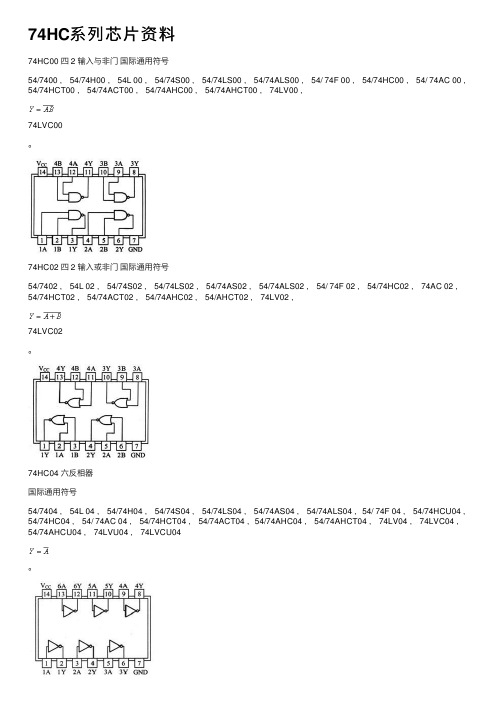
74HC系列芯⽚资料74HC00 四 2 输⼊与⾮门国际通⽤符号54/7400 , 54/74H00 , 54L 00 , 54/74S00 , 54/74LS00 , 54/74ALS00 , 54/ 74F 00 , 54/74HC00 , 54/ 74AC 00 ,54/74HCT00 , 54/74ACT00 , 54/74AHC00 , 54/74AHCT00 , 74LV00 ,74LVC00。
74HC02 四 2 输⼊或⾮门国际通⽤符号54/7402 , 54L 02 , 54/74S02 , 54/74LS02 , 54/74AS02 , 54/74ALS02 , 54/ 74F 02 , 54/74HC02 , 74AC 02 ,54/74HCT02 , 54/74ACT02 , 54/74AHC02 , 54/AHCT02 , 74LV02 ,74LVC02。
74HC04 六反相器国际通⽤符号54/7404 , 54L 04 , 54/74H04 , 54/74S04 , 54/74LS04 , 54/74AS04 , 54/74ALS04 ,54/ 74F 04 , 54/74HCU04 ,54/74HC04 , 54/ 74AC 04 , 54/74HCT04 , 54/74ACT04 ,54/74AHC04 , 54/74AHCT04 , 74LV04 , 74LVC04 ,54/74AHCU04 , 74LVU04 , 74LVCU04。
74HC08 四 2 输⼊与门国际通⽤符号54/7408 , 54/74S08 , 54/74LS08 , 54/74AS08 , 54/74ALS08 , 54/ 74F 08 , 54/74HC08 ,54/74HCT08 , 54/ 74AC 08 , 54/74ACT08 , 54/74AHC08 , 54/74AHCT08 , 74LV08 , 74LVC08。
M74HC4040中文资料

M54/74HC4020M54/74HC4040March 1993HC404012STAGE BINARY COUNTERHC402014STAGE BINARY COUNTER B1R(Plastic Package)ORDER CODES :M54HCXXXF1R M74HCXXXM1R M74HCXXXB1R M74HCXXXC1RF1R(Ceramic Package)M1R(Micro Package)C1R (Chip Carrier)PIN CONNECTION (top view).HIGH SPEEDf MAX =73MHz (TYP.)at V CC =5V .LOW POWER DISSIPATIONI CC =4µA (MAX.)at T A =25oC .HIGH NOISE IMMUNITYV NIH =V NIL =28%V CC (MIN.).OUTPUT DRIVE CAPABILITY 10LSTTL LOADS.SYMMETRICAL OUTPUT IMPEDANCE |I OH |=I OL =4mA (MIN.).BALANCED PROPAGATION DELAYS t PLH =t PHL.WIDE OPERATING VOLTAGE RANGE V CC (OPR)=2V to 6V.PIN AND FUNCTION COMPATIBLE WITH 4020B/4040BDESCRIPTIONThe M54/74HC4020/HC4040are high speedCMOS 14/12-STAGE BINARY COUNTER fabricated in silicon gate C 2MOS technology.They have the same high speed performance of LSTTL combined with true CMOS low consumption.A clear input is used to reset the counter to the all low level state.A high level on CLEAR accomplishes the reset function.A negative transition on the CLOCK input increments the counter by one.For HC4020twelve kind od divided output are provided;1st and 4th stage to 14th stage.The maximum division available at last stage is 1/16384x f IN at clock.For HC4040each division stage has an output;the final frequency is 1/4096x f IN .All inputs are equipp ed with protection circuits against static discharge and transient excess voltage.HC4020HC4040HC4020HC40401/13INPUT AND OUTPUT EQUIVALENT CIRCUITPIN DESCRIPTION (HC4020)PIN No SYMBOL NAME AND FUNCTION 9,7,6,5,3,2,4,13,12,14,15,1Q1,Q4to Q14Parallel Outputs10CLOCK Clock Input (LOW to HIGH,edge triggered)11CLEAR Reset Inputs8GND Ground (0V)16V CCPositive Supply VoltageIEC LOGIC SYMBOLSPIN DESCRIPTION (HC4040)PIN No SYMBOL NAME AND FUNCTION 9,7,6,5,3,2,4,13,12,14,15,1Q1to Q12Parallel Outputs10CLOCK Clock Input (LOW to HIGH,edge triggered)11CLEAR Reset Inputs8GND Ground (0V)16V CCPositive Supply VoltageTRUTH TABLECLOCK CLEAR OUTPUT STATE XH ALL OUTPUTS =”L”L NO CHANGE LADVANCE TO NEXT STATEHC4020HC4040M54/M74HC4020/40402/13M54/M74HC4020/4040 LOGIC DIAGRAM(HC4020)3/13M54/M74HC4020/4040 LOGIC DIAGRAM(HC4040)4/13ABSOLUTE MAXIMUM RATINGSSymbol Parameter Value Unit V CC Supply Voltage-0.5to+7V V I DC Input Voltage-0.5to V CC+0.5V V O DC Output Voltage-0.5to V CC+0.5VI IK DC Input Diode Current±20mAI OK DC Output Diode Current±20mAI O DC Output Source Sink Current Per Output Pin±25mAI CC or I GND DC V CC or Ground Current±50mAP D Power Dissipation500(*)mW T stg Storage Temperature-65to+150o C T L Lead Temperature(10sec)300o C Absolute Maximum Ratings are those values beyond whichdamage to the device may occu r.Functiona l ope ration und er these cond ition isnotimplied. (*)500mW:≅65o C derate to300mW by10mW/o C:65o C to85o CRECOMMENDED OPERATING CONDITIONSSymbol Parameter Value Unit V CC Supply Voltage2to6V V I Input Voltage0to V CC V V O Output Voltage0to V CC VT op Operating Temperature:M54HC SeriesM74HC Series -55to+125-40to+85o Co Ct r,t f Input Rise and Fall Time V CC=2V0to1000nsV CC=4.5V0to500V CC=6V0to400M54/M74HC4020/40405/13DC SPECIFICATIONSSymbol ParameterTest Conditions ValueUnit V CC(V)T A=25o C54HC and74HC-40to85o C74HC-55to125o C54HCMin.Typ.Max.Min.Max.Min.Max.V IH High Level InputVoltage 2.0 1.5 1.5 1.5V 4.5 3.15 3.15 3.156.0 4.2 4.2 4.2V IL Low Level InputVoltage 2.00.50.50.5V 4.5 1.35 1.35 1.356.0 1.8 1.8 1.8V OH High LevelOutput Voltage 2.0V I=V IHorV ILI O=-20µA1.92.0 1.9 1.9V 4.5 4.4 4.5 4.4 4.46.0 5.9 6.0 5.9 5.94.5I O=-4.0mA 4.18 4.31 4.13 4.106.0I O=-5.2mA 5.68 5.8 5.63 5.60V OL Low Level OutputVoltage 2.0V I=V IHorV ILI O=20µA0.00.10.10.1V 4.50.00.10.10.16.00.00.10.10.14.5I O=4.0mA0.170.260.330.406.0I O=5.2mA0.180.260.330.40I I Input LeakageCurrent 6.0V I=V CC or GND±0.1±1±1µAI CC Quiescent SupplyCurrent 6.0V I=V CC or GND44080µAM54/M74HC4020/4040 6/13AC ELECTRICAL CHARACTERISTICS(C L=50pF,Input t r=t f=6ns)Symbol ParameterTest Conditions ValueUnit V CC(V)T A=25o C54HC and74HC-40to85o C74HC-55to125o C54HCMin.Typ.Max.Min.Max.Min.Max.t TLH t THL Output TransitionTime2.0307595110ns4.581519226.07131619t PLH t PHL PropagationDelay Time(Qn-Qn+1)2.020506575ns4.551013156.0491113t PLH t PHL PropagationDelay Time(CLOCK Q1)2.0for HC402076145180220ns4.5212936446.018253138t PLH t PHL PropagationDelay Time(CLOCK Q1)2.0for HC404048145180220ns4.5172936446.013253138t PHL PropagationDelay Time(CLEAR-Qn)2.0for HC402060140175210ns 4.5182835426.015243036t PHL PropagationDelay Time(CLEAR-Qn)2.0for HC404056140175210ns 4.5182835426.015243036f MAX Maximum ClockFrequency 2.0 6.015 4.84MHz 4.5306524206.035702824t W(H) t W(L)Minimum PulseWidth(CLOCK)2.0407595110ns4.581519226.07131619t W(H)Minimum PulseWidth(CLEAR)2.0for HC4020327595110ns 4.581519226.07131619t W(H)Minimum PulseWidth(CLEAR)2.0for HC404070175220265ns 4.5193544536.016303745t REM MinimumRemoval Time 2.0for HC4020000ns 4.50006.0000t REM MinimumRemoval Time 2.0for HC4040253040ns 4.55686.0557C IN Input Capacitance51010pFC PD(*)Power DissipationCapacitance 34pF(*)C PD is defined as the value of the IC’s internal equivalent capac itanc e which is calculated from the operating current con sump tion without load. (Refer to Test Circuit).Average operting current can be obtained by the following equ ation.I CC(opr)=C PD•V CC•f IN+I CC/2(per FLIP/FLOP)M54/M74HC4020/40407/13M54/M74HC4020/4040SWITCHING CHARACTERISTICS TEST WAVEFORMTEST CIRCUIT I CC(Opr.)INPUT WAVEFORM IS THE SAME AS THAT IN CASE OF SWITCHING CHARACTERISTICS TEST. 8/13M54/M74HC4020/4040 Plastic DIP16(0.25)MECHANICAL DATAmm inchDIM.MIN.TYP.MAX.MIN.TYP.MAX.a10.510.020B0.77 1.650.0300.065b0.50.020b10.250.010D200.787E8.50.335e 2.540.100e317.780.700F7.10.280I 5.10.201L 3.30.130Z 1.270.050P001C9/13M54/M74HC4020/4040Ceramic DIP16/1MECHANICAL DATAmm inch DIM.MIN.TYP.MAX.MIN.TYP.MAX.A200.787 B70.276D 3.30.130E0.380.015e317.780.700F 2.29 2.790.0900.110G0.40.550.0160.022H 1.17 1.520.0460.060L0.220.310.0090.012 M0.51 1.270.0200.050 N10.30.406 P7.88.050.3070.317 Q 5.080.200P053D 10/13M54/M74HC4020/4040 SO16(Narrow)MECHANICAL DATAmm inchDIM.MIN.TYP.MAX.MIN.TYP.MAX.A 1.750.068a10.10.20.0040.007a2 1.650.064b0.350.460.0130.018b10.190.250.0070.010C0.50.019c145°(typ.)D9.8100.3850.393E 5.8 6.20.2280.244e 1.270.050e38.890.350F 3.8 4.00.1490.157G 4.6 5.30.1810.208L0.5 1.270.0190.050M0.620.024S8°(max.)P013H11/13M54/M74HC4020/4040PLCC20MECHANICAL DATAmm inch DIM.MIN.TYP.MAX.MIN.TYP.MAX.A9.7810.030.3850.395 B8.899.040.3500.356D 4.2 4.570.1650.180d1 2.540.100d20.560.022E7.378.380.2900.330e 1.270.050e3 5.080.200F0.380.015G0.1010.004 M 1.270.050M1 1.140.045P027A 12/13M54/M74HC4020/4040 Information furnished is believed to be accurate and reliable.However,SGS-THOMSON Microelectronics assumes no responsability for the consequences of use of such information nor for any infringement of patents or other rights of third parties which may results from its use.No license is granted by implication or otherwise under any patent or patent rights of SGS-THOMSON Microelectronics.Specificationsmentioned in this publication are subject to change without notice.This publication supersedes and replaces all information previously supplied.SGS-THOMSON Microelectronics products are not authorized for use ascritical components in life support devices or systems without express written approval of SGS-THOMSON Microelectonics.©1994SGS-THOMSON Microelectronics-All Rights ReservedSGS-THOMSON Microelectronics GROUP OF COMPANIESAustralia-Brazil-France-Germany-Hong Kong-Italy-Japan-Korea-Malaysia-Malta-Morocco-The Netherlands-Singapore-Spain-Sweden-Switzerland-Taiwan-Thailand-United Kingdom-U.S.A13/13。
CD74HC238NSR中文资料
- Bus Driver Outputs . . . . . . . . . . . . . 15 LSTTL Loads
• Wide Operating Temperature Range . . . -55oC to 125oC
• Balanced Propagation Delay and Transition Times
•
Typical CL = 15
Propagation Delay pF, TA = 25oC
of
13
ns
at
VCC
=
5
V,
• Fanout (Over Temperature Range)
- Standard Outputs . . . . . . . . . . . . . . . 10 LSTTL Loads
Two active low and one active high enables (E1, E2, and E3) are provided to ease the cascading of decoders. The decoder’s eight outputs can drive ten low-power Schottky TTL equivalent loads.
CD74HC238M CD74HC238MT CD74HC238M96 CD74HC238NSR CD74HC238PW CD74HC238PWR CD74HC238PWT
-55 to 125 -55 to 125 -55 to 125 -55 to 125 -55 to 125 -55 to 125 -55 to 125
For VO > -0.5V or VO < VCC + 0.5V . . . . . . . . . . . . . . . . . . . .±25mA DC VCC or Ground Current, ICC or IGND . . . . . . . . . . . . . . . . . .±50mA
M74HC4078中文资料
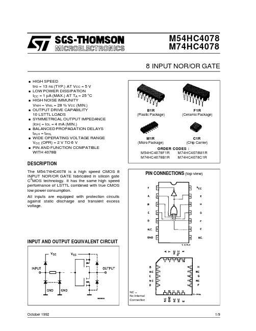
M54HC4078M74HC4078October 19928INPUT NOR/OR GATEB1R(Plastic Package)ORDER CODES :M54HC4078F1R M74HC4078M1R M74HC4078B1R M74HC4078C1RF1R(Ceramic Package)M1R(Micro Package)C1R (Chip Carrier)PIN CONNECTIONS (top view)NC =No Internal Connecti o nINPUT AND OUTPUT EQUIVALENT CIRCUITDESCRIPTION.HIGH SPEEDt PD =13ns (TYP.)AT V CC =5V .LOW POWER DISSIPATION I CC =1µA (MAX.)AT T A =25°C .HIGH NOISE IMMUNITYV NIH =V NIL =28%V CC (MIN.).OUTPUT DRIVE CAPABILITY 10LSTTL LOADS.SYMMETRICAL OUTPUT IMPEDANCE |I OH |=I OL =4mA (MIN.).BALANCED PROPAGATION DELAYS t PLH =t PHL.WIDE OPERATING VOLTAGE RANGE V CC (OPR)=2V TO 6V.PIN AND FUNCTION COMPATIBLE WITH 4078BThe M54/74HC4078is a high speed CMOS 8INPUT NOR/OR GATE fabricated in silicon gate C 2MOS technology.It has the same high speed performance of LSTTL combined with true CMOS low power consumption.All inputs are equipp ed with protection circuits against static discharge and transient excess voltage.1/9TRUTH TABLEINPUTSOUTPUTSX YALL INPUTS”L”H LOTHER POSSIBILITIES L HPIN DESCRIPTIONPIN No SYMBOL NAME AND FUNCTION2,3,4,5,9,10,11,12A to H Data Inputs1,13Y,X Data Outputs7GND Ground(0V)14V CC Positive Supply VoltageIEC LOGIC SYMBOLSCHEMATIC CIRCUITABSOLUTE MAXIMUM RATINGSSymbol Parameter Value Unit V CC Supply Voltage-0.5to+7V V I DC Input Voltage-0.5to V CC+0.5V V O DC Output Voltage-0.5to V CC+0.5VI IK DC Input Diode Current±20mAI OK DC Output Diode Current±20mAI O DC Output Source Sink Current Per Output Pin±25mAI CC or I GND DC V CC or Ground Current±50mAP D Power Dissipation500(*)mW T stg Storage Temperature-65to+150o C T L Lead Temperature(10sec)300o C Absolute Maximum Ratings are those values beyond whichdamage to the device may occu r.Functiona l ope ration und er these cond ition isnotimplied. (*)500mW:≅65o C derate to300mW by10mW/o C:65o C to85o CM54/M74HC40782/9RECOMMENDED OPERATING CONDITIONSSymbol Parameter Value Unit V CC Supply Voltage2to6V V I Input Voltage0to V CC V V O Output Voltage0to V CC VT op Operating Temperature:M54HC SeriesM74HC Series -55to+125-40to+85o Co Ct r,t f Input Rise and Fall Time V CC=2V0to1000nsV CC=4.5V0to500V CC=6V0to400DC SPECIFICATIONSSymbol ParameterTest Conditions ValueUnit V CC(V)T A=25o C54HC and74HC-40to85o C74HC-55to125o C54HCMin.Typ.Max.Min.Max.Min.Max.V IH High Level InputVoltage 2.0 1.5 1.5 1.5V 4.5 3.15 3.15 3.156.0 4.2 4.2 4.2V IL Low Level InputVoltage 2.00.50.50.5V 4.5 1.35 1.35 1.356.0 1.8 1.8 1.8V OH High LevelOutput Voltage 2.0V I=V IHorV ILI O=-20µA1.92.0 1.9 1.9V 4.5 4.4 4.5 4.4 4.46.0 5.9 6.0 5.9 5.94.5I O=-4.0mA 4.18 4.31 4.13 4.106.0I O=-5.2mA 5.68 5.8 5.63 5.60V OL Low Level OutputVoltage 2.0V I=V IHorV ILI O=20µA0.00.10.10.1V 4.50.00.10.10.16.00.00.10.10.14.5I O=4.0mA0.170.260.330.406.0I O=5.2mA0.180.260.330.40I I Input LeakageCurrent 6.0V I=V CC or GND±0.1±1±1µAI CC Quiescent SupplyCurrent 6.0V I=V CC or GND11020µAM54/M74HC40783/9AC ELECTRICAL CHARACTERISTICS (C L =50pF,Input t r =t f =6ns)SymbolParameterTest ConditionsValueUnitV CC (V)T A =25o C 54HC and 74HC -40to 85o C 74HC -55to 125o C54HC Min.Typ.Max.Min.Max.Min.Max.t TLH t THL Output Transition Time 2.0307595110ns 4.581519226.07131619t PLH t PHLPropagation Delay Time2.04895120145ns 4.5121924296.010162025C IN Input Capacitance 5101010pF C PD (*)Power Dissipation Capacitance37pF (*)C PD is defined as the value of the IC’s internal equivalent capac itanc e which is calculated from the operating current con sump tion without load.(Refer to Test Circuit).Average operting current can be obtained by the following equ ation.I CC (opr)=C PD •V CC •f IN +I CCSWITCHING CHARACTERISTICS TEST CIRCUITINPUT WAVEFORM IS THE SAME AS THAT IN CASE OF SWITCHING CHARACTERIS TICS TEST.TEST CIRCUIT I CC (Opr.)M54/M74HC40784/9M54/M74HC4078 Plastic DIP14MECHANICAL DATAmm inchDIM.MIN.TYP.MAX.MIN.TYP.MAX.a10.510.020B 1.39 1.650.0550.065b0.50.020b10.250.010D200.787E8.50.335e 2.540.100e315.240.600F7.10.280I 5.10.201L 3.30.130Z 1.27 2.540.0500.100P001A5/9M54/M74HC4078Ceramic DIP14/1MECHANICAL DATAmm inch DIM.MIN.TYP.MAX.MIN.TYP.MAX.A200.787 B7.00.276D 3.30.130E0.380.015e315.240.600F 2.29 2.790.0900.110G0.40.550.0160.022H 1.17 1.520.0460.060L0.220.310.0090.012 M 1.52 2.540.0600.100 N10.30.406 P7.88.050.3070.317 Q 5.080.200P053C 6/9M54/M74HC4078SO14MECHANICAL DATAmm inchDIM.MIN.TYP.MAX.MIN.TYP.MAX.A 1.750.068a10.10.20.0030.007a2 1.650.064b0.350.460.0130.018b10.190.250.0070.010C0.50.019c145°(typ.)D8.558.750.3360.344E 5.8 6.20.2280.244e 1.270.050e37.620.300F 3.8 4.00.1490.157G 4.6 5.30.1810.208L0.5 1.270.0190.050M0.680.026S8°(max.)P013G7/9M54/M74HC4078PLCC20MECHANICAL DATAmm inch DIM.MIN.TYP.MAX.MIN.TYP.MAX.A9.7810.030.3850.395 B8.899.040.3500.356D 4.2 4.570.1650.180d1 2.540.100d20.560.022E7.378.380.2900.330e 1.270.050e3 5.080.200F0.380.015G0.1010.004 M 1.270.050M1 1.140.045P027A 8/9M54/M74HC4078 Information furnished is believed to be accurate and reliable.However,SGS-THOMSON Microelectronics assumes no responsability for the consequences of use of such information nor for any infringement of patents or other rights of third parties which may results from its use.No license is granted by implication or otherwise under any patent or patent rights of SGS-THOMSON Microelectronics.Specificationsmentioned in this publication are subject to change without notice.This publication supersedes and replaces all information previously supplied.SGS-THOMSON Microelectronics products are not authorized for use ascritical components in life support devices or systems without express written approval of SGS-THOMSON Microelectonics.©1994SGS-THOMSON Microelectronics-All Rights ReservedSGS-THOMSON Microelectronics GROUP OF COMPANIESAustralia-Brazil-France-Germany-Hong Kong-Italy-Japan-Korea-Malaysia-Malta-Morocco-The Netherlands-Singapore-Spain-Sweden-Switzerland-Taiwan-Thailand-United Kingdom-U.S.A9/9。
MC74HC238ADG;MC74HC238ADTG;MC74HC238ADR2G;MC74HC238ADTR2G;中文规格书,Datasheet资料
/
3
MC74HC238AN AWLYYWWG
1
16 1
16
SOIC−16 D SUFFIX CASE 751B
HC238AG AWLYWW
1
16
16 1
TSSOP−16 DT SUFFIX CASE 948F
HC 238A ALYWG
G
1
A WL, L YY, Y WW, W G or G
= Assembly Location = Wafer Lot = Year = Work Week = Pb−Free Package
11 Y4 10
Y5
9 Y6
7 Y7
6
4
PIN 16 = VCC
PIN 8 = GND
5
Figure 2. Logic Diagram
ACTIVE-HIGH OUTPUTS
ORDERING INFORMATION Device
MC74HC238ANG
Package
PDIP−16 (Pb−Free)
Shipping† 500 Units / Rail
Standard No. 7A
• Chip Complexity: 100 FETs or 29 Equivalent Gates • These are Pb−Free Devices*
16 1
MARKING DIAGRAMS
M74HC132中文资料

Value -40 to 85 oC -55 to 125 oC 74HC 54HC Min. Max. Min. Max. 95 19 16 130 26 22 10 110 22 19 160 32 27 10 pF pF ns ns ransition Time Propagation Delay Time
o o
C C
Absolute Maximum Ratings are those values beyond which damage to the device may occur. Functional operation under these condition isnotimplied. (*) 500 mW: ≅ 65 oC derate to 300 mW by 10mW/oC: 65 oC to 85 oC
PIN DESCRIPTION
PIN No 1, 4, 9, 12 2, 5, 10, 13 3, 6, 8, 11 7 14 SYMBOL 1A to 4A 1B to 4B 1Y to 4Y GND VCC NAME AND FUNCTION Data Inputs Data Inputs Data Outputs Ground (0V) Positive Supply Voltage
元器件交易网
M54HC132 M74HC132
QUAD 2-INPUT SCHMITT NAND GATE
. . . . . . . .
HIGH SPEED tPD = 11 ns (TYP.) AT VCC = 5 V LOW POWER DISSIPATION ICC = 1µA (MAX.) AT TA = 25 °C OUTPUT DRIVE CAPABILITY 10 LSTTL LOADS HIGH NOISE IMMUNITY VH (TYP.) = 0.9 V AT VCC = 5 V SYMMETRICAL OUTPUT IMPEDANCE IOH = IOL = 4 mA (MIN.) BALANCED PROPAGATION DELAYS tPLH = tPHL WIDE OPERATING VOLTAGE RANGE VCC (OPR) = 2 V TO 6 V PIN AND FUNCTION COMPATIBLE WITH 54/74LS132
双电源自动切换管理 芯片-概述说明以及解释

双电源自动切换管理芯片-概述说明以及解释1.引言1.1 概述概述部分的内容可以根据双电源自动切换管理芯片的背景和重要性进行阐述。
可以以以下方式进行撰写:在现代社会,电力的稳定供应对于各行各业的运作至关重要。
然而,在某些情况下,电力供应可能会中断或变得不稳定,例如突发的电力故障或其他意外情况。
为了确保设备和系统的连续运行,双电源自动切换管理芯片应运而生。
双电源自动切换管理芯片是一种集成电路芯片,其设计的主要目的是在主电源故障或不稳定时,能够自动切换到备用电源并保持系统的正常运行。
该芯片通过监测主电源的状态以及备用电源的可用性,能够快速而可靠地切换电源,并确保系统能够平稳地工作,减少停机时间和数据丢失的风险。
双电源自动切换管理芯片在各个领域都具有广泛的应用,特别是在对电力供应要求高、对系统连续性要求严格的场景中,如电信基站、工业自动化设备、医疗设备等。
通过使用这种芯片,可以有效地保护设备和系统免受电力故障和变动的影响,提高系统的可靠性和稳定性。
相较于传统的手动切换方式,双电源自动切换管理芯片具有诸多优势。
首先,它能够实现快速的电源切换,减少系统中断的时间,并在切换过程中保持设备的正常运行。
其次,该芯片具有智能化的特性,能够根据电源状态的变化做出切换决策,从而进一步提高系统的稳定性和可靠性。
此外,双电源自动切换管理芯片还具有节能环保的特点,能够减少能源的浪费,符合可持续发展的要求。
尽管双电源自动切换管理芯片在各个领域都有广泛的应用,但仍然存在一些挑战和改进空间。
未来,随着技术的不断进步和创新,我们可以期待这种芯片在功能性、可扩展性和稳定性方面的不断提升,以满足各行业对于电力供应的更高要求。
综上所述,双电源自动切换管理芯片是一种具有重要意义的集成电路芯片,其能够在电力故障或不稳定的情况下,自动切换到备用电源并保持系统的正常运行。
它在提高系统可靠性、减少停机时间和数据丢失风险方面发挥着关键作用,是现代社会各个领域中不可或缺的关键技术之一。
led显示屏模组常用IC的引脚说明

引脚说明符号引脚描述Q0…Q7 8位并行数据输出,其中Q0为第15脚GND 第8脚地Q7’ 第9脚串行数据输出MR 第10脚主复位(低电平)SHCP 第11脚移位寄存器时钟输入STCP 第12脚存储寄存器时钟输入OE 第13脚输出有效(低电平)DS 第14脚串行数据输入VCC 第16脚电源74HC138是一款高速CMOS器件,74HC138引脚兼容低功耗肖特基TTL(LSTTL)系列。
74HC138译码器可接受3位二进制加权地址输入(A0, A1和A2),并当使能时,提供8个互斥的低有效输出(Y0至Y7)。
74HC138特有3个使能输入端:两个低有效(E1和E2)和一个高有效(E3)。
除非E1和E2置低且E3置高,否则74HC138将保持所有输出为高。
利用这种复合使能特性,仅需4片74HC138芯片和1个反相器,即可轻松实现并行扩展,组合成为一个1-32(5线到32线)译码器。
任选一个低有效使能输入端作为数据输入,而把其余的使能输入端作为选通端,则74HC138亦可充当一个8输出多路分配器,未使用的使能输入端必须保持绑定在各自合适的高有效或低有效状态。
74HC138与74HC238逻辑功能一致,只不过74HC138为反相输出。
编辑本段功能CD74HC138 ,CD74HC238和CD74HCT138 , CD74HCT238是高速硅栅CMOS解码器,适合内存地址解码或数据路由应用。
74HC138 作用原理于高性能的存贮译码或要求传输延迟时间短的数据传输系统,在高性能存贮器系统中,用这种译码器可以提高译码系统的效率。
将快速赋能电路用于高速存贮器时,译码器的延迟时间和存贮器的赋能时间通常小于存贮器的典型存取时间,这就是说由肖特基钳位的系统译码器所引起的有效系统延迟可以忽略不计。
HC138 按照三位二进制输入码和赋能输入条件,从8 个输出端中译出一个低电平输出。
两个低电平有效的赋能输入端和一个高电平有效的赋能输入端减少了扩展所需要的外接门或倒相器,扩展成24 线译码器不需外接门;扩展成32 线译码器,只需要接一个外接倒相器。
74系列功能大全
7447 TTL BCD—7段高有效译码/驱动器
7448 TTL BCD—7段译码器/内部上拉输出驱动
74490 TTL 双十进制计数器74491 TTL十位计数器
74498 TTL 八进制移位寄存器
7450 TTL 2-3/2-2输入端双与或非门
74502 TTL 八位逐次逼近反相线驱动器
74367 TTL 4/2线使能输入三态六同相线驱动器
74368 TTL 4/2线使能输入三态六反相线驱动器
7437 TTL 开路输出2输入端四与非缓冲器
74373 TTL 三态同相八D锁存器
74374 TTL 三态反相八D锁存器
74375 TTL 4位双稳态锁存器
74158 TTL 反相输出四2选1数据选择器
7416 TTL 开路输出六反相缓冲/驱动器
74160 TTL 可预置BCD异步清除计数器
74161 TTL 可予制四位二进制异步清除计数器
74162 TTL 可预置BCD同步清除计数器
74163 TTL 可予制四位二进制同步清除计数器
74164 TTL 八位串行入/并行输出移位寄存器
74247 TTL BCD—7段15V输出译码/驱动器
74248 TTL BCD—7段译码/升压输出驱动器
74249 TTL BCD—7段译码/开路输出驱动器
74251 TTL 三态输出8选1数据选择器/复工器
74253 TTL 三态输出双4选1数据选择器/复工器
74256 TTL 双四位可寻址锁存器
74175 TTL 带公共时钟和复位四D触发器
74180 TTL 9位奇数/偶数发生器/校验器
HD74HC238RP中文资料

HD74HC2383-to-8-line Decoder/DemultiplexerREJ03D0593–0200(Previous ADE-205-470)Rev.2.00Jan 31, 2006 DescriptionThe HD74HC238 has 3 binary select inputs (A, B and C). If the device is enabled these inputs determine which one of the eight normally high outputs will go low. Two active low and one active high enables (G1, G2A and G2B) are provided to ease the cascading of decoders.Features• High Speed Operation: t pd (Data to Y) = 15 ns typ (C L = 50 pF)• High Output Current: Fanout of 10 LSTTL Loads• Wide Operating Voltage: V CC = 2 to 6 V• Low Input Current: 1 µA max• Low Quiescent Supply Current: I CC (static) = 4 µA max (Ta = 25°C)• Ordering InformationPart Name Package TypePackage Code(Previous Code)PackageAbbreviationTaping Abbreviation(Quantity)HD74HC238P DILP-16pin PRDP0016AE-B(DP-16FV)P —HD74HC238FPEL SOP-16 pin (JEITA) PRSP0016DH-B(FP-16DAV)FP EL (2,000 pcs/reel)HD74HC238RPEL SOP-16 pin (JEDEC) PRSP0016DG-A(FP-16DNV)RP EL (2,500 pcs/reel)Note: Please consult the sales office for the above package availability.Function TableInputsEnable SelectOutputsG1G2A G2B C B A Y0Y1Y2Y3Y4Y5Y6Y7 X X H X X X L L L L L L L L X H X X X X L L L L L L L L L X X X X X L L L L L L L LH L L L L L H L L L L L L LH L L L L H L H L L L L L LH L L L H L L L H L L L L LH L L L H H L L L H L L L LH L L H L L L L L L H L L LH L L H L H L L L L L H L LH L L H H L L L L L L L H LH L L H H H L L L L L L L H H : High levelL : Low levelX : IrrelevantPin ArrangementLogic DiagramAbsolute Maximum RatingsItem Symbol Ratings UnitSupply voltage range V CC –0.5 to 7.0 V Input / Output voltage V IN , V OUT –0.5 to V CC +0.5 V Input / Output diode current I IK , I OK ±20 mA Output current I O ±35 mA V CC , GND current I CC or I GND ±75 mA Power dissipation P T 500 mW Storage temperature Tstg –65 to +150 °C Note: The absolute maximum ratings are values, which must not individually be exceeded, and furthermore, no two ofwhich may be realized at the same time.Recommended Operating ConditionsItem Symbol Ratings Unit ConditionsSupply voltage V CC 2 to 6 V Input / Output voltage V IN , V OUT 0 to V CC V Operating temperature Ta –40 to 85 °C 0 to 1000 V CC = 2.0 V0 to 500 V CC = 4.5 V Input rise / fall time *1 t r , t f 0 to 400 ns V CC = 6.0 V Notes: 1. This item guarantees maximum limit when one input switches.Waveform: Refer to test circuit of switching characteristics.Electrical CharacteristicsTa = 25°C Ta = –40 to+85°CItem Symbol V CC (V)Min Typ Max Min MaxUnitTest Conditions2.0 1.5 — — 1.5— 4.5 3.15 — — 3.15 — V IH6.0 4.2 — — 4.2 —V 2.0 — — 0.5 — 0.5 4.5 — — 1.35 — 1.35Input voltageV IL6.0 — — 1.8 — 1.8V 2.0 1.9 2.0 — 1.9 — 4.5 4.4 4.5 — 4.4 — 6.0 5.9 6.0 — 5.9 — I OH = –20 µA 4.5 4.18 — — 4.13 — I OH = –4 mA V OH6.0 5.68 — — 5.63— V Vin = V IH or V IL I OH = –5.2 mA2.0 — 0.0 0.1 —0.1 4.5 — 0.0 0.1 — 0.1 6.0 — 0.0 0.1 — 0.1 I OL = 20 µA 4.5 — — 0.26 — 0.33 I OL = 4 mA Output voltage V OL6.0 — — 0.26 —0.33 V Vin = V IH or V IL I OL = 5.2 mA Off-state output currentI OZ 6.0— — ±0.5 — ±5.0 µA Vin = V IH or V IL ,Vout = V CC or GNDInput current Iin 6.0 — — ±0.1 — ±1.0 µA Vin = V CC or GNDQuiescent supply current I CC 6.0— — 4.0 — 40 µA Vin = V CC or GND, Iout = 0 µASwitching Characteristics(C L = 50 pF, Input t r = t f = 6 ns)Ta = 25°C Ta = –40 to +85°CItem Symbol V CC (V)Min Typ Max MinMaxUnit Test Conditions2.0 — — 150 — 190 4.5 — 15 30 — 38 6.0 — — 26 — 33 ns Select to Y 2.0 — — 150 — 190 4.5 — 13 30 — 38 Propagation delaytimet PLHt PHL6.0 — — 26 — 33ns Enable to Y 2.0 — — 75 — 95 4.5 — 5 15 — 19 Output rise/falltimet TLH t THL 6.0 — — 13 — 16 ns Input capacitance Cin— — 5 10 — 10 pFTest CircuitWaveformsPackage Dimensions RENESAS SALES OFFICESRefer to "/en/network" for the latest and detailed information.Renesas Technology America, Inc.450 Holger Way, San Jose, CA 95134-1368, U.S.ATel: <1> (408) 382-7500, Fax: <1> (408) 382-7501Renesas Technology Europe LimitedDukes Meadow, Millboard Road, Bourne End, Buckinghamshire, SL8 5FH, U.K.Tel: <44> (1628) 585-100, Fax: <44> (1628) 585-900Renesas Technology (Shanghai) Co., Ltd.Unit 205, AZIA Center, No.133 Yincheng Rd (n), Pudong District, Shanghai 200120, ChinaTel: <86> (21) 5877-1818, Fax: <86> (21) 6887-7898Renesas Technology Hong Kong Ltd.7th Floor, North Tower, World Finance Centre, Harbour City, 1 Canton Road, Tsimshatsui, Kowloon, Hong KongTel: <852> 2265-6688, Fax: <852> 2730-6071Renesas Technology Taiwan Co., Ltd.10th Floor, No.99, Fushing North Road, Taipei, TaiwanTel: <886> (2) 2715-2888, Fax: <886> (2) 2713-2999Renesas Technology Singapore Pte. Ltd.1 Harbour Front Avenue, #06-10, Keppel Bay Tower, Singapore 098632Tel: <65> 6213-0200, Fax: <65> 6278-8001Renesas Technology Korea Co., Ltd.Kukje Center Bldg. 18th Fl., 191, 2-ka, Hangang-ro, Yongsan-ku, Seoul 140-702, KoreaTel: <82> (2) 796-3115, Fax: <82> (2) 796-2145Renesas Technology Malaysia Sdn. BhdUnit 906, Block B, Menara Amcorp, Amcorp Trade Centre, No.18, Jalan Persiaran Barat, 46050 Petaling Jaya, Selangor Darul Ehsan, MalaysiaTel: <603> 7955-9390, Fax: <603> 7955-9510© 2006. Renesas Technology Corp., All rights reserved. Printed in Japan.。
- 1、下载文档前请自行甄别文档内容的完整性,平台不提供额外的编辑、内容补充、找答案等附加服务。
- 2、"仅部分预览"的文档,不可在线预览部分如存在完整性等问题,可反馈申请退款(可完整预览的文档不适用该条件!)。
- 3、如文档侵犯您的权益,请联系客服反馈,我们会尽快为您处理(人工客服工作时间:9:00-18:30)。
1/10July 2001sHIGH SPEED:t PD = 15ns (TYP .) at V CC = 6V sLOW POWER DISSIPATION:I CC = 4µA(MAX.) at T A =25°C sHIGH NOISE IMMUNITY:V NIH = V NIL = 28 % V CC (MIN.)sSYMMETRICAL OUTPUT IMPEDANCE:|I OH | = I OL = 4mA (MIN)sBALANCED PROPAGATION DELAYS:t PLH ≅ t PHLsWIDE OPERATING VOLTAGE RANGE:V CC (OPR) = 2V to 6VsPIN AND FUNCTION COMPATIBLE WITH 74 SERIES 238DESCRIPTIONThe M74HC238 is an high speed CMOS 3 TO 8LINE DECODER fabricated with silicon gate C 2MOS technology.If the device is enabled, 3 binary select inputs (A,B and C) determine which one of outputs will go high. When enable input G1 is held "Low" or either G2A or G2B is held "High" decoding function isinhibited and all the 8 outputs go low. Three enable inputs are provided to ease cascade connection and application of this address decoder in memory systems.All inputs are equipped with protection circuits against static discharge and transient excess voltage.M74HC2383 TO 8 LINE DECODERPIN CONNECTION AND IEC LOGIC SYMBOLSORDER CODESPACKAGE TUBE T & RDIP M74HC238B1R SOP M74HC238M1RM74HC238RM13TR TSSOPM74HC238TTRM74HC2382/10INPUT AND OUTPUT EQUIVALENT CIRCUITPIN DESCRIPTIONTRUTH TABLEX : Don’t CareLOGIC DIAGRAMPIN No SYMBOL NAME AND FUNCTION 1, 2, 3A, B, C Data Inputs4, 5 G2A G2B Enable Input (Active LOW)6G1Data Enable Input (Active HIGH)15, 14, 13, 12, 11, 10, 9,7Y0 to Y7Outputs8GND Ground (0V)16V CCPositive Supply VoltageINPUTSOUTPUTS SELECTED OUTPUTENABLE SELECTG2B G2A G1C B A Y0Y1Y2Y3Y4Y5Y6Y7X X L X X X L L L L L L L L NONE X H X X X X L L L L L L L L NONE H X X X X X L L L L L L L L NONE L L H L L L H L L L L L L L Y0L L H L L H L H L L L L L L Y1L L H L H L L L H L L L L L Y2L L H L H H L L L H L L L L Y3L L H H L L L L L L H L L L Y4L L H H L H L L L L L H L L Y5L L H H H L L L L L L L H L Y6LLHHHHLLLLLLLHY7M74HC2383/10ABSOLUTE MAXIMUM RATINGSAbsolute Maximum Ratings are those values beyond which damage to the device may occur. Functional operation under these conditions is not implied(*) 500mW at 65 °C; derate to 300mW by 10mW/°C from 65°C to 85°CRECOMMENDED OPERATING CONDITIONSSymbol ParameterValue Unit V CC Supply Voltage -0.5 to +7V V I DC Input Voltage -0.5 to V CC + 0.5V V O DC Output Voltage -0.5 to V CC + 0.5V I IK DC Input Diode Current ± 20mA I OK DC Output Diode Current ± 20mA I O DC Output Current ± 25mA I CC or I GND DC V CC or Ground Current± 50mA P D Power Dissipation 500(*)mW T stg Storage Temperature -65 to +150°C T LLead Temperature (10 sec)300°CSymbol ParameterValue Unit V CC Supply Voltage 2 to 6V V I Input Voltage 0 to V CC V V O Output Voltage 0 to V CC V T op Operating Temperature -55 to 125°C t r , t fInput Rise and Fall TimeV CC = 2.0V 0 to 1000ns V CC = 4.5V 0 to 500ns V CC = 6.0V0 to 400nsM74HC2384/10DC SPECIFICATIONSAC ELECTRICAL CHARACTERISTICS (C L = 50 pF, Input t r = t f = 6ns)SymbolParameterTest ConditionsValue UnitV CC (V)T A = 25°C -40 to 85°C -55 to 125°C Min.Typ.Max.Min.Max.Min.Max.V IHHigh Level Input Voltage2.0 1.5 1.5 1.5V 4.53.15 3.15 3.156.04.24.24.2V ILLow Level Input Voltage2.00.50.50.5V4.5 1.35 1.35 1.356.0 1.81.81.8V OHHigh Level Output Voltage2.0I O =-20 µA 1.9 2.0 1.9 1.9V4.5I O =-20 µA 4.4 4.5 4.4 4.46.0I O =-20 µA5.96.0 5.9 5.94.5I O =-4.0 mA 4.18 4.31 4.13 4.106.0I O =-5.2 mA 5.685.8 5.635.60V OLLow Level Output Voltage2.0I O =20 µA 0.00.10.10.1V 4.5I O =20 µA 0.00.10.10.16.0I O =20 µA 0.00.10.10.14.5I O =4.0 mA 0.170.260.330.406.0I O =5.2 mA 0.180.260.330.40I I Input Leakage Current6.0V I = V CC or GND ± 0.1± 1± 1µA I CCQuiescent Supply Current6.0V I = V CC or GND44080µA SymbolParameterTest ConditionsValue UnitV CC (V)T A = 25°C -40 to 85°C -55 to 125°C Min.Typ.Max.Min.Max.Min.Max.t TLH t THL Output TransitionTime 2.0307595110ns 4.581519226.07131619t PLH t PHL Propagation DelayTime (A, B, C - Y) 2.050150190225ns4.5173038456.015263238t PLH t PHL Propagation DelayTime (G1 - Y) 2.050150190225ns4.5173038456.015263238t PLH t PHL Propagation DelayTime (G2 - Y)2.050150190225ns4.5173038456.015263238M74HC2385/10CAPACITIVE CHARACTERISTICS1) C PD is defined as the value of the IC’s internal equivalent capacitance which is calculated from the operating current consumption without load. (Refer to Test Circuit). Average operating current can be obtained by the following equation. I CC(opr) = C PD x V CC x f IN + I CCTEST CIRCUITL R T = Z OUT of pulse generator (typically 50Ω)SymbolParameterTest ConditionsValue UnitV CC (V)T A = 25°C -40 to 85°C -55 to 125°C Min.Typ.Max.Min.Max.Min.Max.C IN Input Capacitance 5.05101010pF C PDPower Dissipation Capacitance (note 1)5.053pFM74HC2386/10WAVEFORM 1: PROPAGATION DELAY TIMES(f=1MHz; 50% duty cycle)M74HC238Information furnished is believed to be accurate and reliable. However, STMicroelectronics assumes no responsibility for the consequences of use of such information nor for any infringement of patents or other rights of third parties which may result from its use. No license is granted by implication or otherwise under any patent or patent rights of STMicroelectronics. Specifications mentioned in this publication are subject to change without notice. This publication supersedes and replaces all information previously supplied. STMicroelectronics products are not authorized for use as critical components in life support devices or systems without express written approval of STMicroelectronics.© The ST logo is a registered trademark of STMicroelectronics© 2001 STMicroelectronics - Printed in Italy - All Rights ReservedSTMicroelectronics GROUP OF COMPANIESAustralia - Brazil - China - Finland - France - Germany - Hong Kong - India - Italy - Japan - Malaysia - Malta - MoroccoSingapore - Spain - Sweden - Switzerland - United Kingdom© 10/10。