FM24W256-GTR;FM24W256-G;中文规格书,Datasheet资料
nRF24G系列开发板规格书
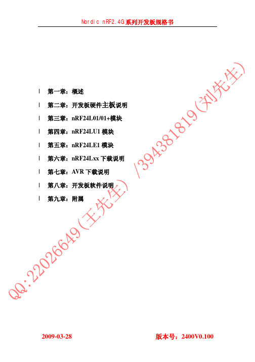
l第一章:概述l第二章:开发板硬件主板说明l第三章:nRF24L01/01+模块l第四章:nRF24LU1模块l第五章:nRF24LE1模块l第六章:nRF24Lxx下载说明l第七章:AVR下载说明l第八章:开发板软件说明l第九章:附属Nordic nRF2400开发板是与nRF24Lx1nRF24LE1)及其ATMega48/88/168结合为(Mega48/88/168)、nRF24L01/01+模块活选择)2.1开发板主板硬件规格2.1-1.开发板版本号: 2.1-2.开发板大小:120mmX120mm 2.1-3.开发板实物:(如下图2-1) 图2-1下载接口电池接口 DC+5V 接口 nRF24LU1/E1模块2.2开发板硬件的组成2.2-1.由A TMega48,8个KEY , 1个复位按钮,8个LED ,7个工作开关,9个连接插针,杜邦跳线及其外部接口组成。
2.2-2.外部接口:RS232接口,USB 接口,+5VDC 接口,外接电池接口,nRF24L01模块接口,nRF24LE1/U1模块接口,A VR 下载ISP 接口,nRF24Lxx 下载接口。
2.2-3.开发板元件位置图(如下图2-2)图2-22.4-1.开发板部件说明位号部件名称部件说明备注U1 nRF24LE1/U1模块接口nRF24LE1/U1 RF 信号传输通道接口部件 2款芯片接口兼容 U2 A TMega48/88/168 A VR 单片机 可选① U3 REG1117-3.3 电源管理IC U4 MAX3232 RS232电平串口通讯 DB1 RS232 (9针头) 与PC 串口连接J1 VBA T 电池座 接备用电池,电压在(4.5V~6V ) J2 Φ5.5mmDC 座 接+5V/500MA 电源适配器 J3 USB 接口与PC 的USB 口连接JP1nRF24LE1/U1模块接与U1(nRF24LE1/U1模块)引脚相2.3-2. “JP1,JP2,JP2JP3线座连JP3”引脚的定义JP4 nRF24L01/01+模块接口nRF24L01/01+ RF信号传输通道接口部件2款芯片接口兼容JP5 nRF24L01/01+接线座与JP4(nRF24L01/01+模块) 引脚相连JP6JP9A VR单片机接线座与A VR单片机引脚相连JP7 nRF24LE1/U1下载座与U1(nRF24LE1/U1模块)下载引脚相连JP8 A VR单片机下载座与A VR单片机下载引脚相连JP10 USB/RS232接线座与USB座和MAX232引脚相连JP11 KEY接线座与K1~K8引脚相连JP12 LED接线座与LED1~LED2引脚相连LED1 ~ LED8 测试IO口指示灯与nRF24LE1/U1 或A VR单片的IO端口相连LED10 系统电源指示灯R8系统电源开关至“ON”状态亮K1 ~ K8 测试IO口按键与nRF24LE1/U1 或A VR单片的IO端口相连K9 复位按键只在nRF24LE1/U1复位时起作用Y1 U2的晶体振荡器自定义R1 U1 nRF24LE1/U1模块电源工作时插至“ON”状态系统电源“ON”有效R2 U2 ATMega48/88/168模块电源工作时插至“ON”状态系统电源“ON”有效R3 nRF24L01/01+模块电源工作时插至“ON”状态系统电源“ON”有效R7 U4 串口通讯模块电源工作时插至“ON”状态系统电源“ON”有效R8 系统电源开关工作时插至“ON”状态系统电源“ON”有效R17 LED(1~8)指示模块电源工作时插至“ON”状态系统电源“ON”有效注意:①表示:A TMaga48, A TMaga88, A TMaga168可选择2.3.对外接口(JPXX)各引脚定义:2.3-1.主要分别详细说明:JP1,JP2,JP3,JP4,JP5,JP6,JP7,JP8,JP9,JP10,JP11,JP122.3-2.位号为“JP1,JP2,JP3”引脚的定义作用:它们是与U1(nRF24LE1/U1)模块相连接。
FM25L04B-GA;FM25L04B-GATR;中文规格书,Datasheet资料
Rev. 3.0 Sept. 2011 /
Ramtron International Corporation 1850 Ramtron Drive, Colorado Springs, CO 80921 (800) 545-FRAM, (719) 481-7000
Page 1 of 13
FM25L04B - Automotive Temp.
WP CS HOLD SCK
Instruction Decode Clock Generator Control Logic Write Protect
64 x 64 FRAM Array
Instruction Register
AEC Q100 Grade 1 Compliant
FM25L04B – Automotive Temp.
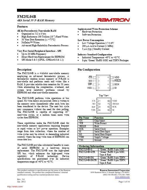
4Kb Serial 3V F-RAM Memory Features
4K bit Ferroelectric Nonvolatile RAM Organized as 512 x 8 bits High Endurance 10 Trillion (1013) Read/Writes NoDelay™ Writes Advanced High-Reliability Ferroelectric Process Fast Serial Peripheral Interface - SPI Up to 10 MHz Frequency Direct Hardware Replacement for EEPROM SPI Mode 0 & 3 (CPOL, CPHA=0,0 & 1,1) Sophisticated Write Protection Scheme Hardware Protection Software Protection Low Power Consumption Low Voltage Operation 3.0-3.6V 6 A Standby Current (+85C) Industry Standard Configuration Automotive Temperature -40C to +125C o Qualified to AEC Q100 Specification 8-pin “Green”/RoHS SOIC Package
24C256_FAIRCHILD_93040
FM24C256 256 KBit 2-Wire Bus Interface Serial EEPROM with Write ProtectFM24C256 256 KBit 2-Wire Bus Interface Serial EEPROM with Write ProtectFM24C256 256 KBit 2-Wire Bus Interface Serial EEPROM with Write ProtectS T O PA C KBus Activity:Master SDA Line 1010Bus ActivityA C KDATAA C KA C KWORD ADDRESS (1)WORD ADDRESS (0)SLAVE ADDRESSS T A RT DEVICE ADDRESSINGFollowing a start condition the master must output the address of the slave it is accessing. The most significant four bits of the slave address are those of the device type identifier. This is fixed as 1010 for all different FM24C256xxx devices.The next three bits identify the device address. Address from 000to 111 are acceptable thus allowing up to eight devices to be connected to the IIC bus.The last bit of the slave address defines whether a write or read condition is requested by the master. A "1" indicates that a READ operation is to be executed and a "0" initiates the WRITE mode.A simple review: After the F M24C256xxx recognizes the start condition, the device interfaced to the IIC bus waits for a slave address to be transmitted over the SDA line. If the transmitted slave address matches an address of one of the devices, the designated slave pulls the SDA line LOW with an acknowledge signal and awaits further transmissions.Write OperationsBYTE WRITEFor a WRITE operation, two additional address fields are required after the control byte acknowledge. These are the word addresses and comprise fifteen bits to provide access to any one of the 32K words. The first byte indicates the high-order byte of the word address. Only the seven least signicant bits can be changed, the most significant bit is pre-assigned the value "0". Following the acknowledgement from the first word address, the next byte indicates the low-order byte of the word address. Upon receipt of the word address, the F M24C256xxx responds with another acknowledge and waits for the next eight bits of data, again,responding with an acknowledge. The master then terminates thetransfer by generating a stop condition, at which time the FM24C256xxx begins the internal write cycle to the nonvolatile memory. While the internal write cycle is in progress, the device's inputs are disabled and the device will not respond to any requests from the master. Refer to Figure 5 for the address, acknowledge and data transfer sequence.PAGE WRITEThe FM24C256xxx is capable of 64 byte page write operation. It is initiated in the same manner as the byte write operation; but instead of terminating the write cycle after the first data word is transferred, the master can transmit up to 63 more words. After the receipt of each word, the device responds with an acknowl-edge.After the receipt of each word, the internal address counter increments to the next address and the next SDA data is ac-cepted. If the master should transmit more than 64 words prior to generating the stop condition, the address counter will "roll over"and the previous written data will be overwritten. As with the byte write operation, all inputs are disabled until completion of the internal write cycle. Refer to Figure 6 for the address, acknowl-edge and data transfer sequence.Acknowledge PollingOnce the stop condition is isssued to indicate the end of the host's write operation, the F M24C256xxx initiates the internal write cycle. ACK polling can be initiated immediately. This involves issuing the start condition followed by the slave address for a write operation. If the FM24C256xxx is still busy with the write opera-tion, no ACK will be returned. If the device has completed the write operation, an ACK will be returned and the host can then proceed with the next read or write operation.DS800023-8Byte Write (Figure 5)FM24C256 256 KBit 2-Wire Bus Interface Serial EEPROM with Write ProtectFM24C256 256 KBit 2-Wire Bus Interface Serial EEPROM with Write Protect。
FM24CL16B-GTR;FM24CL16B-DGTR;FM24CL16B-DG;FM24CL16B-G;中文规格书,Datasheet资料
Two-wire Interface
The FM24CL16B employs a bi-directional two-wire bus protocol using few pins and little board space. Figure 2 illustrates a typical system configuration using the FM24CL16B in a microcontroller-based system. The industry standard two-wire bus is familiar to many users but is described in this section. By convention, any device that is sending data onto the bus is the transmitter while the target device for this data is the receiver. The device that is controlling the bus is the master. The master is responsible for generating the clock signal for all operations. Any device on the bus that is being controlled is a slave. The FM24CL16B is always a slave device. The bus protocol is controlled by transition states in the SDA and SCL signals. There are four conditions including Start, Stop, Data bit, and Acknowledge. Figure 3 illustrates the signal conditions that define the four states. Detailed timing diagrams are in the electrical specifications.
FM25L04B-GTR;FM25L04B-G;FM25L04B-DGTR;FM25L04B-DG;中文规格书,Datasheet资料
Description
The FM25L04B is a 4-kilobit nonvolatile memory employing an advanced ferroelectric process. A ferroelectric random access memory or F-RAM is nonvolatile and performs reads and writes like a RAM. It provides reliable data retention for 38 years while eliminating the complexities, overhead, and system level reliability problems caused by EEPROM and other nonvolatile memories. The FM25L04B performs write operations at bus speed. No write delays are incurred. Data is written to the memory array immediately after each byte has been transferred to the device. The next bus cycle may commence without the need for data polling. The FM25L04B is capable of supporting 10 14 read/write cycles, or a million times more write cycles than EEPROM. These capabilities make the FM25L04B ideal for nonvolatile memory applications requiring frequent or rapid writes or low power operation. Examples range from data collection, where the number of write cycles may be critical, to demanding industrial controls where the long write time of EEPROM can cause data loss. The FM25L04B provides substantial benefits to users of serial EEPROM as a hardware drop-in replacement. The FM25L04B uses the high-speed SPI bus, which enhances the high-speed write capability of F-RAM technology. Device specifications are guaranteed over an industrial temperature range of -40°C to +85°C.
fm24c256读写例程

fm24c256读写例程以下是一个使用FM24C256读写例程的示例。
此例程用于Arduino Uno 和Arduino Mega等Arduino系列微控制器。
注意:该代码没有对写入数据进行任何形式的检查或校验,仅供理解代码使用。
实际应用中需要对数据正确性和一致性进行检查和校验。
```cppinclude <>include <>define FM24C256_CS 10 // 定义FM24C256的片选引脚为10void setup() {(9600);(); // 初始化SPI总线pinMode(FM24C256_CS, OUTPUT); // 将片选引脚设置为输出模式}void loop() {// 写入数据uint8_t writeData[3] = {0x01, 0x02, 0x03}; // 要写入的数据 (0x50); // 开始传输到地址为0x50的设备(writeData, 3); // 写入数据(); // 结束传输delay(100); // 等待一段时间以确保写入完成// 读取数据(0x50); // 开始传输到地址为0x50的设备(); // 结束传输(0x50, 3); // 从地址为0x50的设备请求3个字节的数据while (() < 3) { // 等待数据可用delay(1);}uint8_t readData[3]; // 用于存储读取的数据for (int i = 0; i < 3; i++) {readData[i] = (); // 读取数据}("Read data: ");(readData[0]);(", ");(readData[1]); (", ");(readData[2]); }```。
FM24C1024A_ds_chs

器件/页 地址脚(A2,A1):A2、A1 是硬件连接的器 件地址输入引脚(或空接),可作为和其他 FM24CXX 系列器件的兼容引脚。当这些引脚作为硬件连接的地
17volt25volt55volt符号参数最小值最大值最小值最大值最小值最大值单位fbscl输入时钟频率40010001000khztblow时钟脉宽低电平时间1300400400nstbhigh时钟脉宽高电平时间600400400nstb噪声抑制时间1005050nstbaa时钟低至数据有效时间1009005055050550nstbbuf两次指令间的总线空闲时间1300500500nstbhdsta起始条件保持时间600250250nstbsusta起始条件建立时间600250250nsnstbsudat数据建立时间100100100nstb输入上升时间300300300nstb输入下降时间300100100nstbsusto停止条件建立时间600250250nstbdh数据输出保持时间505050nstbwrmsendurance50v25c页操作模式1000000writecycles交流参数测试条件
FM24C1024A 两线制串行 EEPROM
技术手册
7
器件操作
时钟及数据传输:SDA 引脚通常被外围器件拉高。SDA 引脚的数据应在 SCL 为低时变化(参见图 4);当数据 在 SCL 为高时变化,将视为下文所述的一个起始或停 止命令。
向 EEPROM 返回一个应答信号。收到该应答信号后, EEPROM 会继续输出下一组 8 位的数据。若此时没有 得到主控器件的应答信号,EEPROM 会停止读出数据, 直到主控器件返回一个停止命令来结束读周期。
FM24V02-GTR;FM24V02-G;中文规格书,Datasheet资料
Two-wire Interface
The FM24V02 employs a bi-directional two-wire bus protocol using few pins or board space. Figure 2 illustrates a typical system configuration using the FM24V02 in a microcontroller-based system. The industry standard two-wire bus is familiar to many users but is described in this section. By convention, any device that is sending data onto the bus is the transmitter while the target device for this data is the receiver. The device that is controlling the bus is the master. The master is responsible for generating the clock signal for all operations. Any device on the bus that is being controlled is a slave. The FM24V02 always is a slave device. The bus protocol is controlled by transition states in the SDA and SCL signals. There are four conditions including start, stop, data bit, or acknowledge. Figure 3 illustrates the signal conditions that specify the four states. Detailed timing diagrams are shown in the electrical specifications section.
FM24W256
* Not Recommended for New Designs
Ramtron International Corporation 1850 Ramtron Drive, Colorado Springs, CO 80921 (800) 545-FRAM, (719) 481-7000
Pre-Production
FM24W256
256Kb Wide Voltage Serial F-RAM Features
256K bit Ferroelectric Nonvolatile RAM Organized as 32,768 x 8 bits High Endurance 100 Trillion (1014) Read/Writes 38 year Data Retention (@ +75ºC) NoDelay™ Writes Advanced High-Reliability Ferroelectric Process Fast Two-wire Serial Interface Up to 1 MHz maximum bus frequency Direct hardware replacement for EEPROM Supports legacy timing for 100 kHz & 400 kHz Low Power Operation Wide Voltage Operation 2.7V-5.5V 100 A Active Current (100 kHz) 15 A Standby Current (typ.) Industry Standard Configuration Industrial Temperature -40 C to +85 C 8-pin “Green”/RoHS SOIC Package
FM24C64B-GTR;FM24C64B-G;中文规格书,Datasheet资料
Ramtron International Corporation 1850 Ramtron Drive, Colorado Springs, CO 80921 (800) 545-FRAM, (719) 481-7000 Page 1 of 12
/
FM24C64B
Counter
Address Latch
1,024 x 64 FRAM Array
8
SDA
Serial to Parallel Converter
Data Latch
SCL WP A0-A2 Control Logic
Figure 1. FM24C64B Block Diagram Pin Description Pin Name A0-A2 I/O Input Pin Description Address 2-0: These pins are used to select one of up to 8 devices of the same type on the same two-wire bus. To select the device, the address value on the three pins must match the corresponding bits contained in the device address. The address pins are pulled down internally. Serial Data Address: This is a bi-directional pin used to shift serial data and addresses for the two-wire interface. It employs an open-drain output and is intended to be wireOR’d with other devices on the two -wire bus. The input buffer incorporates a Schmitt trigger for noise immunity and the output driver includes slope control for falling edges. A pull-up resistor is required. Serial Clock: The serial clock input for the two-wire interface. Data is clocked out of the device on the SCL falling edge, and clocked in on the SCL rising edge. The SCL input also incorporates a Schmitt trigger input for improved noise immunity. Write Protect: When WP is high, the entire array is write-protected. When WP is low, all addresses may be written. This pin is pulled down internally. Supply Voltage: 5V Ground
CAT24WC256中文资料
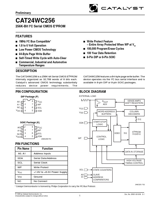
1A1NC V SSA1NC V CC WP SCL SDAA0V CC WP SCL SDAV SSA0PIN FUNCTIONSPin Name FunctionA0, A1Address Inputs SDA Serial Data/Address SCL Serial Clock WP Write ProtectV CC +1.8V to +6.0V Power Supply V SS Ground NCNo ConnectDESCRIPTIONThe CAT24WC256 is a 256K-bit Serial CMOS E 2PROM internally organized as 32,768 words of 8 bits each.Catalyst’s advanced CMOS technology substantially reduces device power requirements. ThePreliminary* Catalyst Semiconductor is licensed by Philips Corporation to carry the I 2C Bus Protocol.s Write Protect Feature– Entire Array Protected When WP at V IHs 100,000 Program/Erase Cycles s 100 Year Data Retention s 8-Pin DIP or 8-Pin SOICCAT24WC256 features a 64-byte page write buffer. The device operates via the I 2C bus serial interface and is available in 8-pin DIP or 8-pin SOIC packages.PIN CONFIGURATIONBLOCK DIAGRAM24WC256 F02CAT24WC256256K-Bit I 2C Serial CMOS E 2PROM s 1MHz I 2C Bus Compatible*s 1.8 to 6 Volt Operation s Low Power CMOS Technology s 64-Byte Page Write Buffers Self-Timed Write Cycle with Auto-Clear s Commercial, Industrial and AutomotiveTemperature RangesFEATURESDIP Package (P)24WC256 F01© 1998 by Catalyst Semiconductor, Inc.Characteristics subject to change without noticeV EXTERNAL LOADV Doc. No. 25061-00 6/99 S-1PreliminaryCAT24WC2562Doc. No. 25061-00 6/99 S-1ABSOLUTE MAXIMUM RATINGS*Temperature Under Bias .................–55°C to +125°C Storage Temperature.......................–65°C to +150°C Voltage on Any Pin withRespect to Ground (1)...........–2.0V to +V CC + 2.0V V CC with Respect to Ground ...............–2.0V to +7.0V Package Power DissipationCapability (Ta = 25°C)...................................1.0W Lead Soldering Temperature (10 secs)............300°C Output Short Circuit Current (2)........................100mA *COMMENTStresses above those listed under “Absolute Maximum Ratings” may cause permanent damage to the device.These are stress ratings only, and functional operation of the device at these or any other conditions outside of those listed in the operational sections of this specification is not implied. Exposure to any absolute maximum rating for extended periods may affect device performance and reliability.RELIABILITY CHARACTERISTICS Symbol Parameter Min.Max.Units Reference Test Method N END (3)Endurance 100,000Cycles/Byte MIL-STD-883, Test Method 1033T DR (3)Data Retention 100Years MIL-STD-883, Test Method 1008V ZAP (3)ESD Susceptibility 2000Volts MIL-STD-883, Test Method 3015I LTH (3)(4)Latch-up100mAJEDEC Standard 17CAPACITANCE T A = 25°C, f = 1.0 MHz, V CC = 5V Symbol TestMax.Units Conditions C I/O (3)Input/Output Capacitance (SDA)8pF V I/O = 0V C IN (3)Input Capacitance (SCL, WP, A0, A1)6pFV IN = 0VNote:(1)The minimum DC input voltage is –0.5V. During transitions, inputs may undershoot to –2.0V for periods of less than 20 ns. Maximum DCvoltage on output pins is V CC +0.5V, which may overshoot to V CC + 2.0V for periods of less than 20ns.(2)Output shorted for no more than one second. No more than one output shorted at a time.(3)This parameter is tested initially and after a design or process change that affects the parameter.(4)Latch-up protection is provided for stresses up to 100 mA on address and data pins from –1V to V CC +1V.(5)Standby current (I SB ) = 0 µA (<900 nA).LimitsSymbol Parameter Min.Typ.Max. Units Test Conditions I CC1Power Supply Current - Read 1mA f SCL = 100 KHz V CC =5V I CC2Power Supply Current - Write 3mA f SCL = 100KHz V CC =5VI SB (5)Standby Current 0µA V IN = GND or V CC V CC =5VI LI Input Leakage Current 1µA V IN = GND to V CC I LO Output Leakage Current 1µA V OUT = GND to V CCV IL Input Low Voltage –1V CC x 0.3V V IH Input High VoltageV CC x 0.7V CC + 0.5V V OL1Output Low Voltage (V CC = +3.0V)0.4V I OL = 3.0 mA V OL2Output Low Voltage (V CC = +1.8V)0.5VI OL = 1.5 mA D.C. OPERATING CHARACTERISTICSV CC = +1.8V to +6.0V, unless otherwise specified.PreliminaryCAT24WC2563Doc. No. 25061-00 6/99 S-1Power-Up Timing (2)(3)Symbol ParameterMax.Units t PUR Power-Up to Read Operation 1ms t PUWPower-Up to Write Operation1msNote:(1) AC measurement conditions:RL (connects to V CC ): 0.3V CC to 0.7 V CC Input rise and fall times: < 50nsInput and output timing reference voltages: 0.5 V CC(2)This parameter is tested initially and after a design or process change that affects the parameter.(3)t PUR and t PUW are the delays required from the time V CC is stable until the specified operation can be initiated.The write cycle time is the time from a valid stop condition of a write sequence to the end of the internal program/erase cycle. During the write cycle, the bus interface circuits are disabled, SDA is allowed to remain high, and the device does not respond to its slave address.A.C. CHARACTERISTICSV CC = +1.8V to +6V, unless otherwise specified Output Load is 1 TTL Gate and 100pF Read & Write Cycle LimitsPreliminaryCAT24WC2564Doc. No. 25061-00 6/99 S-1FUNCTIONAL DESCRIPTIONThe CAT24WC256 supports the I 2C Bus data transmis-sion protocol. This Inter-Integrated Circuit Bus protocol defines any device that sends data to the bus to be a transmitter and any device receiving data to be a re-ceiver. The transfer is controlled by the Master device which generates the serial clock and all START and STOP conditions for bus access. The CAT24WC256operates as a Slave device. Both the Master device and Slave device can operate as either transmitter or re-ceiver, but the Master device controls which mode is activated.PIN DESCRIPTIONS SCL: Serial ClockThe serial clock input clocks all data transferred into or out of the device.SDA: Serial Data/AddressThe bidirectional serial data/address pin is used to transfer all data into and out of the device. The SDA pin is an open drain output and can be wire-ORed with other open drain or open collector outputs.WP: Write ProtectThis input, when tied to GND, allows write operations to the entire memory. When this pin is tied to Vcc, the entire memory is write protected. When left floating,memory is unprotected.5020 FHD F05Figure 3. Start/Stop TimingSTART BITSDASTOP BITSCL5020 FHD F04STOPCONDITIONSTARTCONDITIONADDRESSSCLSDA5020 FHD F03SCLSDA INSDA OUTA0, A1: Device Address InputsThese pins are hardwired or left connected. When hardwired, up to four CAT24WC256's may be addressed on a single bus system. When the pins are left uncon-nected, the default values are zero.PreliminaryCAT24WC2565Doc. No. 25061-00 6/99 S-1The features of the I 2C bus protocol are defined as follows:(1)Data transfer may be initiated only when the bus isnot busy.(2)During a data transfer, the data line must remainstable whenever the clock line is high. Any changes in the data line while the clock line is high will be interpreted as a START or STOP condition.START ConditionThe START Condition precedes all commands to the device, and is defined as a HIGH to LOW transition of SDA when SCL is HIGH. The CAT24WC256 monitors the SDA and SCL lines and will not respond until this condition is met.STOP ConditionA LOW to HIGH transition of SDA when SCL is HIGH determines the STOP condition. All operations must end with a STOP condition.DEVICE ADDRESSINGThe bus Master begins a transmission by sending a START condition. The Master sends the address of the particular slave device it is requesting. The five most significant bits of the 8-bit slave address are fixed as 10100(Fig. 5). The CAT24WC256 uses the next two bits as address bits. The address bits A1 and A0 allow as Figure 4. Acknowledge Timing5027 FHD F07Figure 5. Slave Address Bits5020 FHD F06ACKNOWLEDGESTARTSCL FROM MASTERDATA OUTPUTFROM TRANSMITTERDATA OUTPUT FROM RECEIVERmany as four devices on the same bus. These bits must compare to their hardwired input pins. The last bit of the slave address specifies whether a Read or Write opera-tion is to be performed. When this bit is set to 1, a Read operation is selected, and when set to 0, a Write opera-tion is selected.After the Master sends a START condition and the slave address byte, the CAT24WC256 monitors the bus and responds with an acknowledge (on the SDA line) whenits address matches the transmitted slave address. The CAT24WC256 then performs a Read or Write operation depending on the state of the R/W bit.AcknowledgeAfter a successful data transfer, each receiving device is required to generate an acknowledge. The Acknowledg-ing device pulls down the SDA line during the ninth clock cycle, signaling that it received the 8 bits of data.The CAT24WC256 responds with an acknowledge after receiving a START condition and its slave address. If the device has been selected along with a write operation,it responds with an acknowledge after receiving each 8-bit byte.When the CAT24WC256 begins a READ mode it trans-mits 8 bits of data, releases the SDA line, and monitors the line for an acknowledge. Once it receives this ac-knowledge, the CAT24WC256 will continue to transmit data. If no acknowledge is sent by the Master, the deviceI 2C BUS PROTOCOLPreliminaryCAT24WC2566Doc. No. 25061-00 6/99 S-1terminates data transmission and waits for a STOP condition.WRITE OPERATIONSByte WriteIn the Byte Write mode, the Master device sends the START condition and the slave address information (with the R/W bit set to zero) to the Slave device. After the Slave generates an acknowledge, the Master sends two 8-bit address words that are to be written into the address pointers of the CAT24WC256. After receiving another acknowledge from the Slave, the Master device transmits the data to be written into the addressed memory location. The CAT24WC256 acknowledges once more and the Master generates the STOP condi-tion. At this time, the device begins an internal program-ming cycle to nonvolatile memory. While the cycle is in progress, the device will not respond to any request from the Master device.Page WriteThe CAT24WC256 writes up to 64 bytes of data, in a single write cycle, using the Page Write operation. The page write operation is initiated in the same manner as the byte write operation, however instead of terminating after the initial byte is transmitted, the Master is allowed to send up to 63 additional bytes. After each byte has been transmitted, CAT24WC256 will respond with an acknowledge, and internally increment the six low order address bits by one. The high order bits remain un-changed.If the Master transmits more than 64 bytes before sending the STOP condition, the address counter ‘wraps around’,and previously transmitted data will be overwritten.When all 64 bytes are received, and the STOP condition has been sent by the Master, the internal programming cycle begins. At this point, all received data is written to the CAT24WC256 in a single write cycle.Acknowledge PollingDisabling of the inputs can be used to take advantage of the typical write cycle time. Once the stop condition is issued to indicate the end of the host's write operation,CAT24WC256 initiates the internal write cycle. ACK polling can be initiated immediately. This involves issu-ing the start condition followed by the slave address for a write operation. If CAT24WC256 is still busy with the write operation, no ACK will be returned. If CAT24WC256 has completed the write operation, an ACK will be returned and the host can then proceed with the next read or write operation.WRITE PROTECTIONThe Write Protection feature allows the user to protect against inadvertent programming of the memory array.If the WP pin is tied to V CC , the entire memory array is protected and becomes read only. The CAT24WC256will accept both slave and byte addresses, but the memory location accessed is protected from program-ming by the device’s failure to send an acknowledge after the first byte of data is received.24WC256F09Figure 7. Page Write TimingFigure 6. Byte Write Timing24WC256 F08*=Don't Care BitA 15–A 8SLAVE ADDRESSSA C KA C K DATAA C K ST O P PBUS ACTIVITY:MASTERSDA LINES T A R T A 7–A 0BYTE ADDRESS A C K*SLAVE C KC K C K BUS ACTIVITY:MASTERSDA LINES T A R BYTE ADDRESS C K ST O C KC K C K *=Don't Care BitPreliminaryCAT24WC2567Doc. No. 25061-00 6/99 S-1READ OPERATIONSThe READ operation for the CAT24WC256 is initiated in the same manner as the write operation with one excep-tion, that R/W bit is set to one. Three different READ operations are possible: Immediate/Current Address READ, Selective/Random READ and Sequential READ.Immediate/Current Address ReadThe CAT24WC256’s address counter contains the ad-dress of the last byte accessed, incremented by one. In other words, if the last READ or WRITE access was to address N, the READ immediately following would ac-cess data from address N+1. If N=E (where E=32767),then the counter will ‘wrap around’ to address 0 and continue to clock out data. After the CAT24WC256set to one), it issues an acknowledge, then transmits the 8 bit byte requested. The master device does not send an acknowledge, but will generate a STOP condition.Selective/Random ReadSelective/Random READ operations allow the Master device to select at random any memory location for a READ operation. The Master device first performs a ‘dummy’ write operation by sending the START condi-tion, slave address and byte addresses of the location itwishes to read. After CAT24WC256 acknowledges, the Master device sends the START condition and the slave address again, this time with the R/W bit set to one. The CAT24WC256 then responds with its acknowledge and sends the 8-bit byte requested. The master device does not send an acknowledge but will generate a STOP condition.Sequential ReadThe Sequential READ operation can be initiated by either the Immediate Address READ or Selective READ operations. After the CAT24WC256 sends the initial 8-bit byte requested, the Master will respond with an acknowledge which tells the device it requires more data. The CAT24WC256 will continue to output an 8-bit byte for each acknowledge sent by the Master. The operation will terminate when the Master fails to respond with an acknowledge, thus sending the STOP condition.The data being transmitted from CAT24WC256 is out-putted sequentially with data from address N followed by data from address N+1. The READ operation address counter increments all of the CAT24WC256 address bits so that the entire memory array can be read during one operation. If more than E (where E=32767) bytes are read out, the counter will ‘wrap around’ and continue to clock out data bytes.Figure 8. Immediate Address Read Timing24WC256 F1024WC128 F10SCL SDA 8TH BIT STOPNO ACKDATA OUT89SLAVE ADDRESSSA C KBUS ACTIVITY:MASTERSDA LINES T A R T N O A C KDATAS T O P PPreliminaryCAT24WC2568Doc. No. 25061-00 6/99 S-1Figure 9. Selective Read TimingORDERING INFORMATIONNotes:(1) The device used in the above example is a 24WC256KI-1.8TE13 (SOIC, Industrial Temperature, 1.8 Volt to 6 Volt OperatingVoltage, Tape & Reel)5020 FHD F12BUS ACTIVITY:MASTERSDA LINEDATA n+xDATA n C KC KDATA n+1C KS TO O A C KDATA n+2C KSLAVEADDRESS24WC256 FIG. 11*=Don't Care BitA –A SLAVE ADDRESSA C KA C KA C KBUS ACTIVITY:MASTERSDA LINES T A R A –A BYTE ADDRESS SLAVEADDRESSA C KN O A C KS T A R DATAS T O CAT。
at24c256中文手册

a t24c256中文手册(总4页) -CAL-FENGHAI.-(YICAI)-Company One1-CAL-本页仅作为文档封面,使用请直接删除AT24C256中文资料2009-11-15 09:43特性与1MHz I2C 总线兼容1.8 到6.0 伏工作电压范围低功耗CMOS 技术写保护功能当WP 为高电平时进入写保护状态64 字节页写缓冲器自定时擦写周期100,000 编程/擦写周期可保存数据100 年8 脚DIP SOIC 封装温度范围商业级工业级和汽车级概述CAT24WC256 是一个256K 位串行CMOS E2PROM 内部含有32768 个字节每字节为8 位CATALYST 公司的先进CMOS 技术实质上减少了器件的功耗CAT24WC256 有一个64 字节页写缓冲器该器件通过I2C 总线接口进行操作管脚描述管脚名称功能A0 A1 地址输入SDA 串行数据/地址SCL 串行时钟WP 写保护Vcc +1.8V 6.0V 电源Vss 地NC 未连接极限参数工作温度工业级-55 +125商业级0 +75贮存温度-65 +150各管脚承受电压-2.0V Vcc+2.0VVcc 管脚承受电压-2.0V +7.0V封装功率损耗Ta=25 1.0W 焊接温度(10 秒) 300口输出短路电流100mA功能描述CAT24WC256 支持I2C 总线数据传送协议I2C 总线协议规定任何将数据传送到总线的器件作为发送器任何从总线接收数据的器件为接收器数据传送是由产生串行时钟和所有起始停止信号的主器件控制的CAT24WC256 是作为从器件被操作的主器件和从器件都可以作为发送器或接收器但由主器件控制传送数据发送或接收的模式管脚描述SCL 串行时钟CAT24WC256 串行时钟输入管脚用于产生器件所有数据发送或接收的时钟这是一个输入管脚SDA 串行数据/地址双向串行数据/地址管脚用于器件所有数据的发送或接收SDA 是一个开漏输出管脚可与其它开漏输出或集电极开路输出进行线或wire-ORWP 写保护当WP 脚连接到Vcc 所有内存变成写保护只能读当WP 引脚连接到Vss 或悬空允许器件进行读/写操作A0 A1 器件地址输入这些管脚为硬连线或者不连接对于单总线系统最多可寻址4 个CAT24WC256 器件参阅器件寻址当这些引脚没有连接时其默认值为0I2C 总线协议I2C 总线协议定义如下1 只有在总线空闲时才允许启动数据传送2 在数据传送过程中当时钟线为高电平时数据线必须保持稳定状态不允许有跳变时钟线为高电平时数据线的任何电平变化将被看作总线的起始或停止信号起始信号时钟线保持高电平期间数据线电平从高到低的跳变作为I2C 总线的起始信号停止信号时钟线保持高电平期间数据线电平从低到高的跳变作为I2C 总线的停止信号器件寻址主器件通过发送一个起始信号启动发送过程然后发送它所要寻址的从器件的地址8 位从器件地址的高5 位固定为10100 见图5 接下来的2 位A1 A0 为器件的地址位最多可以连接4 个器件到同一总线上这些位必须与硬连线输入脚A1 A0 相对应从器件地址的最低位作为读写控制位1表示对从器件进行读操作0 表示对从器件进行写操作在主器件发送起始信号和从器件地址字节后CAT24WC256 监视总线并当其地址与发送的从地址相符时响应一个应答信号通过SDA 线CAT24WC256 再根据读写控制位R/W 的状态进行读或写操作应答信号I2C 总线数据传送时每成功地传送一个字节数据后接收器都必须产生一个应答信号应答的器件在第9 个时钟周期时将SDA 线拉低表示其已收到一个8 位数据CAT24WC256 在接收到起始信号和从器件地址之后响应一个应答信号如果器件已选择了写操作则在每接收一个8 位字节之后响应一个应答信号当CAT24WC256 工作于读模式时在发送一个8 位数据后释放SDA 线并监视一个应答信号一旦接收到应答信号CAT24WC256 继续发送数据如主器件没有发送应答信号器件停止传送数据并等待一个停止信号写操作字节写在字节写模式下主器件发送起始信号和从器件地址信息R/W 位置0 给从器件在从器件送回应答信号后主器件发送两个8 位地址字写入CAT24WC256 的地址指针主器件在收到从器件的应答信号后再发送数据到被寻址的存储单元CAT24WC256 再次应答并在主器件产生停止信号后开始内部数据的擦写在内部擦写过程中CAT24WC256 不再应答主器件的任何请求页写在页写模式下单个写周期内CAT24WC256 最多可以写入64 个字节数据页写操作的启动和字节写一样不同在于传送了一字节数据后主器件允许继续发送63 个字节每发送一个字节后CAT24WC256 将响应一个应答位且内部低6 位地址加1 高位地址保持不变如果主器件在发送停止信号之前发送大于64 个字节地址计数器将自动翻转先前写入的数据被覆盖当所有64 字节接收完毕主器件发送停止信号内部编程周期开始此时所有接收到的数据在单个写周期内写入CAT24WC256应答查询可以利用内部写周期时禁止数据输入这一特性一旦主器件发送停止位指示主器件操作结束时CAT24WC256 启动内部写周期应答查询立即启动包括发送一个起始信号和进行写操作的从器件地址如果CAT24WC256 正在进行内部写操作将不会发送应答信号如果CAT24WC256 已经完成了内部写操作将发送一个应答信号主器件可以继续对CAT24WC256 进行下一次读写操作写保护写保护操作特性可使用户避免由于不当操作而造成对存储区域内部数据的改写当WP 管脚接高时整个寄存器区全部被保护起来而变为只可读取CAT24WC256 可以接收从器件地址和字节地址但是装置在接收到第一个数据字节后不发送应答信号从而避免寄存器区域被编程改写读操作CAT24WC256 读操作的初始化方式和写操作时一样仅把R/W 位置为1 有三种不同的读操作方式立即/当前地址读选择/随机读和连续读立即/当前地址读的地址计数器内容为最后操作字节的地址加1 也就是说如果上次读/写的操作地址为N 则立即读的地址从地址N+1 开始如果N=E 此处E=32767 则计数器将翻转到0 且继续输出数据CAT24WC256接收到从器件地址信号后R/W 位置1 它首先发送一个应答信号然后发送一个8 位字节数据主器件不需发送一个应答信号但要产生一个停止信号选择/随机读选择/随机读操作允许主器件对寄存器的任意字节进行读操作主器件首先通过发送起始信号从器件地址和它想读取的字节数据的地址执行一个伪写操作在CAT24WC256 应答之后主器件重新发送起始信号和从器件地址此时R/W 位置1 CAT24WC256 响应并发送应答信号然后输出所要求的一个8 位字节数据主器件不发送应答信号但产生一个停止信号连续读连续读操作可通过立即读或选择性读操作启动在CAT24WC256 发送完一个8 位字节数据后主器件产生一个应答信号来响应告知CAT24WC256 主器件要求更多的数据对应每个主机产生的应答信号CAT24WC256 将发送一个8 位数据字节当主器件不发送应答信号而发送停止位时结束此操作从CAT24WC256 输出的数据按顺序由N 到N+1 输出读操作时地址计数器在CAT24WC256 整个地址内增加这样整个寄存器区域在可在一个读操作内全部读出当读取的字节超过E 此处E=32767计数器将翻转到零并继续输出数据字节。
FM24C16B-GTR;FM24C16B-G;中文规格书,Datasheet资料
Ordering Information
FM24C16B-G FM24C16B-GTR “Green”/RoHS 8-pin SOIC “Green”/RoHS 8-pin SOIC, Tape & Reel
This product conforms to specifications per the terms of the Ramtron standard warranty. The product has completed Ramtron’s internal qualification testing and has reached production status. Rev. 3.0 Jan. 2012
FM24C16B - 16Kb 5V I2C F-RAM
Counter
Address Latch
256 x 64 FRAM Array
8
SDA
`
Serial to Parallel Converter
Data Latch
SCL WP Control Logic
Figure 1. Block Diagram Pin Description Pin Name SDA Type I/O Pin Description Serial Data Address: This is a bi-directional data pin for the two-wire interface. It employs an open-drain output and is intended to be wire-OR’d with other devices on the two-wire bus. The input buffer incorporates a Schmitt trigger for noise immunity and the output driver includes slope control for falling edges. A pull-up resistor is required. Serial Clock: The serial clock input for the two-wire interface. Data is clocked-out on the falling edge and clocked-in on the rising edge. Write Protect: When WP is igh, the entire array is write-protected. When WP is low, all addresses may be written. This pin is internally pulled down. Supply Voltage (5V) Ground No connect
CAT24C256WI-GT3中文资料

256-Kb I 2C CMOS Serial EEPROMCAT24C256PIn COnfIguRATIOn funCTIOnAl SyMbOlfEATuRESn Supports Standard and fast I 2C Protocol n 1.8 V to 5.5 V Supply Voltage Range n 64-byte Page Write buffern Hardware Write Protection for entire memory n Schmitt Triggers and noise Suppression filterson I 2C bus Inputs (SCl and SDA).n low power CMOS technology n 1,000,000 program/erase cycles n 100 year data retention n Industrial temperature rangen RoHS-compliant 8-pin PDIP and SOIC packagesPDIP (l)SOIC (W, X)VSSSD ASCL WPA 2, A 1, A 0DEVICE DESCRIPTIOnThe CAT24C256 is a 256-Kb Serial CMOS EEPROM, internally organized as 5 2 pages of 64 bytes each, for a total of 32,768 bytes of 8 bits each.It features a 64-byte page write buffer and supports both the Standard ( 00 kHz) as well as Fast (400 kHz) I 2C protocol.Write operations can be inhibited by taking the WP pin High (this protects the entire memory).External address pins make it possible to address up to eight CAT24C256 devices on the same bus.8765V CC WP SCL SDAA 2A 0A 1V SS1234For the location of Pin , please consult the corresponding package drawing.PIn funCTIOnSA 0, A, A 2Device Address SDA Serial Data SCL Serial Clock WP Write Protect V CC Power Supply V SSGround* Catalyst carries the I 2C protocol under a license from the Philips Corporation.for Ordering Information details, see page 13.CAT24C256AbSOluTE MAXIMuM RATIngS(1)Storage Temperature-65°C to + 50°C Voltage on Any Pin with Respect to Ground(2)-0.5 V to +6.5 VRElIAbIlITy CHARACTERISTICS(3)Symbol Parameter Min unitsN END(4)Endurance ,000,000Program/ Erase Cycles T DR Data Retention 00YearsD.C. OPERATIng CHARACTERISTICSV CC = .8 V to 5.5 V, T A = -40°C to 85°C, unless otherwise specified.Symbol Parameter Test Conditions Min Max unitsI CC Supply Current Read or Write at 400 kHz mAI SB Standby Current All I/O Pins at GND or V CC µAI L I/O Pin Leakage Pin at GND or V CC µAV IL Input Low Voltage-0.5V CC x 0.3V V IH Input High Voltage V CC x 0.7V CC + 0.5V V OL Output Low Voltage V CC > 2.5 V, I OL = 3.0 mA0.4V V OL2Output Low Voltage V CC > .8 V, I OL = .0 mA0.2VPIn IMPEDAnCE CHARACTERISTICST A = 25°C, f = 400 kHz, V CC = 5 VSymbol Parameter Conditions Min Max unitsC IN(3)SDA I/O Pin Capacitance V IN = 0 V8pFC IN(3)Input Capacitance (other pins)V IN = 0 V6pFnotes:( ) Stresses above those listed under “Absolute Maximum Ratings” may cause permanent damage to the device. These are stress ratings only, and functional operation of the device at these or any other conditions outside of those listed in the operational sections of this specification is not implied. Exposure to any absolute maximum rating for extended periods may affect device performance and reliability.(2) The DC input voltage on any pin should not be lower than -0.5 V or higher than V CC + 0.5 V. During transitions, the voltage on any pin mayundershoot to no less than - .5 V or overshoot to no more than V CC + .5 V, for periods of less than 20 ns.(3) These parameters are tested initially and after a design or process change that affects the parameter according to appropriate AEC-Q 00and JEDEC test methods.(4) Page Mode, V CC = 5 V, 25°CCAT24C256A.C. CHARACTERISTICS(1)V CC = .8 V to 5.5 V, T A = -40°C to 85°C, unless otherwise specified.Symbol Parameter1.8 V - 5.5 V2.5 V - 5.5 Vunits Min Max Min MaxF SCL Clock Frequency 00400kHzT I(2)Noise Suppression Time Constant atSCL, SDA Inputs0. 0. µst AA SCL Low to SDA Data Out 3.50.9µs t BUF(2)Time the Bus Must be Free Before aNew Transmission Can Start4.7 .3µst HD:STA Start Condition Hold Time40.6µs t LOW Clock Low Period 4.7 .3µs t HIGH Clock High Period40.6µs t SU:STA Start Condition Setup Time 4.70.6µs t HD:DAT Data In Hold Time00µs t SU:DAT Data In Setup Time0.250. µs t R(2)SDA and SCL Rise Time 0.3µs t F(2)SDA and SCL Fall Time0.30.3µs t SU:STO Stop Condition Setup Time40.6µs t DH Data Out Hold Time0. 0. µs t WR Write Cycle Time55ms t PU(2), (3)Power-up to Ready Mode ms notes:( ) Test conditions according to “A.C. Test Conditions” table.(2) Tested initially and after a design or process change that affects this parameter.(3) t PU is the delay between the time V CC is stable and the device is ready to accept commands.A.C. TEST COnDITIOnSInput Levels0.2 x V CC to 0.8 x V CCInput Rise and Fall Times≤ 50 nsInput Reference Levels0.3 x V CC, 0.7 x V CCOutput Reference Levels0.5 x V CCOutput Load Current Source: I OL = 3 mA (V CC≥ 2.5 V); I OL = mA (V CC < 2.5 V); C L = 00 pFCAT24C256PIn DESCRIPTIOnSCl:The Serial Clock input pin accepts the Serial Clock generated by the Master.SDA: The Serial Data I/O pin receives input data and transmits data stored in EEPROM. In transmit mode, this pin is open drain. Data is acquired on the positive edge, and is delivered on the negative edge of SCL.A0, A1 and A2: The Address pins accept the device ad-dress. These pins have on-chip pull-down resistors. WP: The Write Protect input pin inhibits all write op-erations, when pulled HIGH. This pin has an on-chip pull-down resistor.funCTIOnAl DESCRIPTIOnThe CAT24C256 supports the Inter-Integrated Circuit (I2C) Bus data transmission protocol, which defines a device that sends data to the bus as a transmitter and a device receiving data as a receiver. Data flow is controlled by a Master device, which generates the serial clock and all START and STOP conditions. The CAT24C256 acts as a Slave device. Master and Slave alternate as either transmitter or receiver. Up to 8 devices may be connected to the bus as determined by the device ad-dress inputs A0, A , and A2.I2C buS PROTOCOlThe I2C bus consists of two ‘wires’, SCL and SDA. The two wires are connected to the V CC supply via pull-up resistors. Master and Slave devices connect to the 2-wire bus via their respective SCL and SDA pins. The transmitting device pulls down the SDA line to ‘transmit’ a ‘0’ and releases it to ‘transmit’ a ‘ ’.Data transfer may be initiated only when the bus is not busy (see A.C. Characteristics).During data transfer, the SDA line must remain stable while the SCL line is HIGH. An SDA transition while SCL is HIGH will be interpreted as a START or STOP condition (Figure ).STARTThe START condition precedes all commands. It consists of a HIGH to LOW transition on SDA while SCL is HIGH. The START acts as a ‘wake-up’ call to all receivers. A bsent a START, a Slave will not respond to commands. STOPThe STOP condition completes all commands. It consists of a LOW to HIGH transition on SDA while SCL is HIGH. The STOP starts the internal Write cycle (when follow-ing a Write command) or sends the Slave into standby mode (when following a Read command).Device AddressingThe Master initiates data transfer by creating a START condition on the bus. The Master then broadcasts an 8-bit serial Slave address. The first 4 bits of the Slave address are set to 0 0, for normal Read/Write opera-tions (Figure 2). The next 3 bits, A2, A and A0, select one of 8 possible Slave devices. The last bit, R/W, specifies whether a Read (1) or Write (0) operation is to be performed.AcknowledgeAfter processing the Slave address, the Slave responds with an acknowledge (ACK) by pulling down the SDA line during the 9th clock cycle (Figure 3). The Slave will also acknowledge the byte address and every data byte presented in Write mode. In Read mode the Slave shifts out a data byte, and then releases the SDA line during the 9th clock cycle. If the Master acknowledges the data, then the Slave continues transmitting. The Master terminates the session by not acknowledging the last data byte (NoACK) and by sending a STOP to the Slave. Bus timing is illustrated in Figure 4.CAT24C256figure 3. Acknowledge Timingfigure 2. Slave Address bitsfigure 1. Start/Stop Timingfigure 4. bus TimingSCLSDA INSDA OUTCAT24C256WRITE OPERATIOnSbyte WriteIn Byte Write mode the Master sends a START, followed by Slave address, two byte address and data to be written (Figure 5). The Slave acknowledges all 4 bytes, and the Master then follows up with a STOP, which in turn starts the internal Write operation (Figure 6). During internal Write, the Slave will not acknowledge any Read or Write request from the Master.Page WriteThe CAT24C256 contains 32,768 bytes of data, arranged in 5 2 pages of 64 bytes each. A two byte address word, following the Slave address, points to the first byte to be written. The most significant bit of the address word is ‘don’t care’, the next 9 bits identify the page and the last 6 bits identify the byte within the page. Up to 64 bytes can be written in one Write cycle (Figure 7).The internal byte address counter is automatically in-cremented after each data byte is loaded. If the Master transmits more than 64 data bytes, then earlier bytes will be overwritten by later bytes in a ‘wrap-around’ fashion (within the selected page). The internal Write cycle starts immediately following the STOP.Acknowledge PollingAcknowledge polling can be used to determine if the CAT24C256 is busy writing or is ready to accept com-mands. Polling is implemented by interrogating the device with a ‘Selective Read’ command (see READ OPERATIONS).The CAT24C256 will not acknowledge the Slave address, as long as internal Write is in progress.Hardware Write ProtectionWith the WP pin held HIGH, the entire memory is pro-tected against Write operations. If the WP pin is left floating or is grounded, it has no impact on the operation of the CAT24C256.CAT24C256 figure 5. byte Write Timingfigure 6. Write Cycle Timingfigure 7. Page Write TimingCAT24C256READ OPERATIOnSImmediate Address ReadIn standby mode, the CAT24C256 internal address counter points to the data byte immediately following the last byte accessed by a previous operation. If that ‘previ-ous’ byte was the last byte in memory, then the address counter will point to the st memory byte, etc. When, following a START, the CAT24C256 is presented with a Slave address containing a ‘ ’ in the R/W bit position (Figure 8), it will acknowledge (ACK) in the 9th clock cycle, and will then transmit data being pointed at by the internal address counter. The Master can stop further transmission by issuing a NoACK, followed by a STOP condition.Selective ReadThe Read operation can also be started at an address different from the one stored in the internal address counter. The address counter can be initialized by per-forming a ‘dummy’ Write operation (Figure 9). Here the START is followed by the Slave address (with the R/W bit set to ‘0’) and the desired two byte address. Instead of following up with data, the Master then issues a 2nd START, followed by the ‘Immediate Address Read’ se-quence, as described earlier.Sequential ReadIf the Master acknowledges the st data byte transmitted by the CAT24C256, then the device will continue trans-mitting as long as each data byte is acknowledged by the Master (Figure 0). If the end of memory is reached during sequential Read, then the address counter will ‘wrap-around’ to the beginning of memory, etc. Sequential Read works with either ‘Immediate Address Read’ or ‘Selective Read’, the only difference being the starting byte address.CAT24C256 figure 8. Immediate Address Read Timingfigure 9. Selective Read Timingfigure 10. Sequential Read TimingCAT24C2568-lEAD 300 MIl WIDE PlASTIC DIP (l)notes:( ) Complies with JEDEC Standard MS00 .(2) All dimensions are in millimeters.(3) Dimensioning and tolerancing per ANSI Y 4.5M- 982ecSYMBOLA A1b b2D E E1e eB LMIN 0.380.369.027.626.09 6.357.872.923.81NOM 0.46 1.771.147.872.54 BSCMAX 4.57A2 3.05 3.810.56c 0.210.260.3510.168.257.119.65For current Tape and Reel information, download the PDF file from:/documents/tapeandreel.pdfPACKAgE OuTlInESCAT24C256Doc No. 04, Rev. D© 2007 by Catalyst Semiconductor, Inc.Characteristics subject to change without notice8-lEAD 150 MIl WIDE SOIC (W)notes:(1) Complies with JEDEC specification MS-012 dimensions.(2) All linear dimensions are in millimeters.SyMbOl A A b C D E E h L MIn 0. 0 .350.334.805.803.800.250.40nOM 0.250. 9MAX 0.25 .750.5 5.006.204.00e .27 BSC0.50 .27Ө10°8°eFor current Tape and Reel information, download the PDF file from:/documents/tapeandreel.pdfCAT24C2562Doc. No. 04, Rev. D© 2007 by Catalyst Semiconductor, Inc.Characteristics subject to change without notice8-lEAD 208 MIl WIDE SOIC, EIAJ (X)notes:(1) Complies with EIAJ specification.(2) All linear dimensions are in millimeters.θcSYMBOLA1A b c D E E1e L MIN 0.050.365.137.755.130.51NOM 0.250.19 1.27 BSCMAX 0.252.030.485.338.265.380.76θ10°8°For current Tape and Reel information, download the PDF file from:/documents/tapeandreel.pdfCAT24C2563Doc No. 04, Rev. D© 2007 by Catalyst Semiconductor, Inc.Characteristics subject to change without noticeORDERIng InfORMATIOnNotes:( ) All packages are RoHS-compliant (Lead-free, Halogen-free). (2) The standard lead finish is NiPdAu.(3) The device used in the above example is a CAT24C256WI-GT3 (SOIC-JEDEC, Industrial Temperature, NiPdAu, Tape & Reel). (4) For SOIC, EIAJ (X) package the standard lead finish is Matte-Tin. This package is available in 2000 pcs/reel, i.e. CAT24C256XI-T2. (5) For additional package and temperature options, please contact your nearest Catalyst Semiconductor Sales office.Catalyst Semiconductor, Inc.Corporate Headquarters 2975 Stender Way Santa Clara, CA 95054Phone: 408.542. 000Fax: 408.542. Copyrights, Trademarks and PatentsTrademarks and registered trademarks of Catalyst Semiconductor include each of the following: Beyond Memory™, DPP™, EZDim™, MiniPot™, and Quad-Mode™Catalyst Semiconductor has been issued U.S. and foreign patents and has patent applications pending that protect its products.CATALYST SEMICONDUCTOR MAKES NO WARRANTY , REPRESENTATION OR GUARANTEE, EXPRESS OR IMPLIED, REGARDING THE SUITABILITY OF ITS PRODUCTS FOR ANY PARTICULAR PURPOSE, NOR THAT THE USE OF ITS PRODUCTS WILL NOT INFRINGE ITS INTELLECTUAL PROPERTY RIGHTS OR THE RIGHTS OF THIRD PARTIES WITH RESPECT TO ANY PARTICULAR USE OR APPLICATION AND SPECIFICALLY DISCLAIMS ANY AND ALL LIABILITY ARISING OUT OF ANY SUCH USE OR APPLICATION, INCLUDING BUT NOT LIMITED TO, CONSEQUENTIAL OR INCIDENTAL DAMAGES.Catalyst Semiconductor products are not designed, intended, or authorized for use as components in systems intended for surgical implant into the body, or other applications intended to support or sustain life, or for any other application in which the failure of the Catalyst Semiconductor product could create a situation where personal injury or death may occur.Catalyst Semiconductor reserves the right to make changes to or discontinue any product or service described herein without notice. Products with data sheets labeled “Advance Information” or “Preliminary” and other products described herein may not be in production or offered for sale.Catalyst Semiconductor advises customers to obtain the current version of the relevant product information before placing orders. Circuit diagrams illustrate typical semiconductor applications and may not be complete.Publication #: 04Revison: D Issue date: 0 / 2/07REVISIOn HISTORyDate Revision Comments0/07/05A Initial Issue/ 6/05B Update Ordering Information Add Tape and Reel Specifications 02/02/06CUpdate Ordering Information0 / 2/07DUpdate Package Outlines. Add SOIC, EIAJ Package Outlines Update A.C. Characteristics. Add A.C. Test ConditionsUpdate Figures , 3 and 4Delete Package Marking. Deleted Tape and Reel Updated Ordering Information。
FM25640B-GTR;FM25640B-G;中文规格书,Datasheet资料

Pin Configuration
CS SO WP VSS
1 2 3 4
8 7 6 5
VDD HOLD SCK SI
Pin Names /CS /HOLD /WP SCK SI SO VDD VSS
Function Chip Select Hold Write Protect Serial Clock Serial Data Input Serial Data Output 5V Ground
Description
The FM25640B is a 64-kilobit nonvolatile memory employing an advanced ferroelectric process. A ferroelectric random access memory or F-RAM is nonvolatile but operates in other respects as a RAM. It provides reliable data retention for 38 years while eliminating the complexities, overhead, and system level reliability problems caused by EEPROM and other nonvolatile memories. The FM25640B performs write operations at bus speed. No write delays are incurred. Data is written to the memory array immediately after it has been successfully transferred to the device. The next bus cycle may commence immediately without the need for data polling. The FM25640B is capable of supporting up to 1012 read/write cycles, or a million times more write cycles than EEPROM. These capabilities make the FM25640B ideal for nonvolatile memory applications requiring frequent or rapid writes. Examples range from data collection, where the number of write cycles may be critical, to demanding industrial controls where the long write time of EEPROM can cause data loss. The FM25640B provides substantial benefits to users of serial EEPROM, in a hardware drop-in replacement. The FM25640B uses the high-speed SPI bus, which enhances the high-speed write capability of F-RAM technology. The specifications are guaranteed over an industrial temperature range of -40°C to +85°C.
铁电存储器FM24C256在电子仪表中的应用
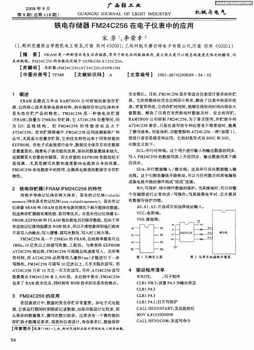
Vc c
单片机
^1
^
WP
SL c S^ D
7 5
待 时间 , A 2 C 5 而 T 4 2 6必须等 待几毫秒 ( ) ms才能进 行下一步 写操作 。 M2 C 5 F 4 2 6可读写 1 亿 次以上 , 0 几乎无 限次读写。而
AT 4 2 6只有 1 2C 5 0万之一百万次读写 。 另外 , T 4 2 6 写 A 2C 5 读
且 功耗 低 。F 2 C 5 M 4 2 6的 性 能远 优 越 于 E P E ROM T 4 5 。 A 2 C2 6
【 关键词 】 存贮器; 2C 5;T 4 26 E R M F 4 26A 2C 5; P O M E 【 中图分 类号 】T3 8 P6 【 文献标识码 】 A 【 文章编号 】 10—63 08 9 5 — 2 0327( 0) — 4 0 2 0
宋 芳 , 荣幸 z 李
(. 1郑州交通职业学院机 电工程 系, 河南 郑州 4 0 0 ; . 5 0 1 2郑州航天赛世特电子有限公司, 河南 郑州 4 0 0 ) 5 0 1
【 摘 要 】 F A R M是一种新型非易 失性存 储器, 常用于断电 后的 数据保存, 最大特点是可以随总 线速度无限次的擦写, 而
或 集 电极 开 路 的 器件 构 成 “ 或 ” 接 。 线 连
2 铁 电存 贮器 ( R F AM ) M2 C2 6的特 性 F 4 5
传 统半导 体记忆 体有两 大体系 :易 失性记忆体 (oai v lte l me r ) moy和非易失性记忆体 n n v lte m r) o — oai oy 。易失性记 lme 忆体像 S M和 D M在没有 电源的情况下都不能保存数据。 RA RA
FM24CL04B-GTR;FM24CL04B-G;中文规格书,Datasheet资料
4Kb Serial 3V F-RAM Memory Features
4K bit Ferroelectric Nonvolatile RAM Organized as 512 x 8 bits High Endurance 1014 Read/Writes 38 Year Data Retention NoDelay™ Writes Advanced High-Reliability Ferroelectric Process Fast Two-wire Serial Interface Up to 1 MHz maximum bus frequency Direct hardware replacement for EEPROM Supports legacy timing for 100 kHz & 400 kHz Low Power Operation 2.7V to 3.65V operation 100 A Active Current (100 kHz) 3 A (typ.) Standby Current Industry Standard Configuration Industrial Temperature -40 C to +85 C 8-pin “Green”/RoHS SOIC (-G)
Pin Configuration
NC A1 A2 VSS
ቤተ መጻሕፍቲ ባይዱ
1 2 3 4
8 7 6 5
VDD WP SCL SDA
Pin Names A1-A2 SDA SCL WP VSS VDD
Function Device Select Address 1 and 2 Serial Data/Address Serial Clock Write Protect Ground Supply Voltage
G24 规格书

(6mm stacking height). • Mounting: Two 2.4 mm holes • Weight: 10.1 gram Environmental • Operating re:
protocol stack
EDGE - model dependant • Multi slot class 10 (4 Down; 2 Up;
5 Total) • Max BR Downlink 236.8 Kbps
(Over RS232) • Coding Scheme MCS1-MCS9 CSD • Max BR 14.4 Kbps SMS • MO / MT Text and PDU modes • Cell broadcast
24.4 mm
Actual size
45.2 mm
In th
e Auto At
Work
The G24 GSM Module, a lead-free product, conforming to the RoHS standard, is one of the most compact modules available and is ideally suited for a wide range of M2M applications, including: • Security and Tracking • Telemetry and Automated Meter Reading
AT COMMAND SET • GSM 07.05 • GSM 07.07 • GSM 07.10 • Motorola proprietary AT
RF24L01中文详细资料 datasheet

待机模式 低电平
掉电模式 -
待机模式 待机模式 I 在保证快速启动的同时减少系统平均消耗电流 在待机模式 I 下 晶振正常工作 在待机
模式 II 下部分时钟缓冲器处在工作模式 当发送端 TX FIFO 寄存器为空并且 CE 为高电平时进入待机模式 II 在待机模式期间 寄存器配置字内容保持不变
掉电模式 在掉电模式下,nRF24L01 各功能关闭 保持电流消耗最小 进入掉电模式后 nRF24L01 停止工作
描述 确认信号 应答信号 自动重发 芯片使能 时钟信号 循环冗余校验 片选非 增强型 ShockBrustTM 高斯键控频移 中断请求 工业 科学 医学 低噪声放大 最低有效位 最低有效字节 兆位/秒 微控制器 主机输入从机输出 主机输出从机输入 最高有效位 最高有效字节 印刷电路板 数据包误码率 数据包识别位 载波 接收源 发射源 掉电 上电 接收 接收数据准备就绪 串行可编程接口 发送 已发送数据
引脚及其功能
引脚 1 2 3 4 5 6 7 8 9 10 11 12 13 14 15 16 17 18 19 20
名称 CE CSN SCK MOSI MISO IRQ VDD VSS XC2 XC1 VDD_PA ANT1 ANT2 VSS VDD IREF VSS VDD DVDD VSS
掉电模式和待机模式下电流消耗更低
快速参考数据
参数
数值
最低供电电压
1.9
最大发射功率
0
最大数据传输率
2000
发射模式下 电流消耗 0dBm
11.3
接收模式下电流消耗 2000kbps
12.3
温度范围
-40~ +85
数据传输率为 1000kbps 下的灵敏度
- 1、下载文档前请自行甄别文档内容的完整性,平台不提供额外的编辑、内容补充、找答案等附加服务。
- 2、"仅部分预览"的文档,不可在线预览部分如存在完整性等问题,可反馈申请退款(可完整预览的文档不适用该条件!)。
- 3、如文档侵犯您的权益,请联系客服反馈,我们会尽快为您处理(人工客服工作时间:9:00-18:30)。
Rev. 2.0 Jan. 2012 /
Page 1 of 13
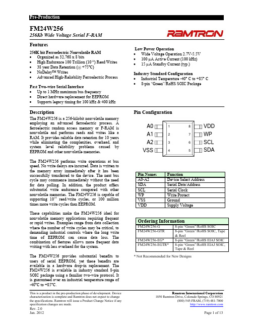
FM24W256 - 256Kb Wide Voltage I2C F-RAM
Counter
Address Latch
4,096 x 64 FRAM Array
8 SDA Serial to Parallel Converter
Description
The FM24W256 is a 256-kilobit nonvolatile memory employing an advanced ferroelectric process. A ferroelectric random access memory or F-RAM is nonvolatile and performs reads and writes like a RAM. It provides reliable data retention for 10 years while eliminating the complexities, overhead, and system level reliability problems caused by EEPROM and other nonvolatile memories. The FM24W256 performs write operations at bus speed. No write delays are incurred. Data is written to the memory array immediately after it has been successfully transferred to the device. The next bus cycle may commence immediately without the need for data polling. In addition, the product offers substantial write endurance compared with other nonvolatile memories. The FM24W256 is capable of supporting 1014 read/write cycles, or 100 million times more write cycles than EEPROM. These capabilities make the FM24W256 ideal for nonvolatile memory applications requiring frequent or rapid writes. Examples range from data collection where the number of write cycles may be critical, to demanding industrial controls where the long write time of EEPROM can cause data loss. The combination of features allows more frequent data writing with less overhead for the system. The FM24W256 provides substantial benefits to users of serial EEPROM, yet these benefits are available in a hardware drop-in replacement. The FM24W256 is available in industry standard 8-pin SOIC package using a familiar two-wire protocol. It is guaranteed over an industrial temperature range of -40°C to +85°C.
Two-wire Interface
The FM24W256 employs a bi-directional two-wire bus protocol using few pins or board space. Figure 2 illustrates a typical system configuration using the FM24W256 in a microcontroller-based system. The industry standard two-wire bus is familiar to many users but is described in this section. By convention, any device that is sending data onto the bus is the transmitter while the target device for this data is the receiver. The device that is controlling the bus is the master. The master is responsible for generating the clock signal for all operations. Any device on the bus that is being controlled is a slave. The FM24W256 always is a slave device. The bus protocol is controlled by transition states in the SDA and SCL signals. There are four conditions including start, stop, data bit, or acknowledge. Figure 3 illustrates the signal conditions that specify the four states. Detailed timing diagrams are in the electrical specifications.
Ordering Information
FM24W256-G FM24W256-GTR FM24W256-EG* FM24W256-EGTR* 8-pin “Green”/RoHS SOIC 8-pin “Green”/RoHS SOIC, Tape & Reel 8-pin “Green”/RoHS EIAJ SOIC 8-pin “Green”/RoHS EIAJ SOIC, Tape & Reel
Pin Configuration
A0 A1 A2 VSS
1 2 3 4
8 7 6 5
VDD WP SCL SDA
Pin Names A0-A2 SDA SCL WP VSS VDD
Function Device Select Address Serial Data/Address Serial Clock Write Protect Ground Supply Voltage
Data Latch
SCL WP A0-A2 Control gic
Figure 1. Block Diagram Pin Description Pin Name A0-A2 Type Input Pin Description Device Select Address 0-2: These pins are used to select one of up to 8 devices of the same type on the same two-wire bus. To select the device, the address value on the three pins must match the corresponding bits contained in the slave address. The address pins are pulled down internally. Serial Data/Address: This is a bi-directional pin for the two-wire interface. It is open-drain and is intended to be wire-OR’d with other devices on the two-wire bus. The input buffer incorporates a Schmitt trigger for noise immunity and the output driver includes slope control for falling edges. A pull-up resistor is required. Serial Clock: The serial clock pin for the two-wire interface. Data is clocked out of the part on the falling edge, and into the device on the rising edge. The SCL input also incorporates a Schmitt trigger input for noise immunity. Write Protect: When tied to VDD, addresses in the entire memory map will be writeprotected. When WP is connected to ground, all addresses may be written. This pin is pulled down internally. Supply Voltage: 2.7V to 5.5V Ground