CC1210AX5R110K中文资料
ioLogik E1200系列产品(E1210)更新说明书

Firmware for ioLogik E1200 Series (E1210) Release NotesSupported Operating SystemsNotesChangesApplicable ProductsBugs FixedN/A• Fixed inaccurate counter value when using Modbus to start a pulse (E1210/E1212/E1213).• Fixed opposite on/off pulse width display on web console (E1211/E1212/E1214).• Fixed that the offset scaling value will reset after changing the Alias name (E1260).• Fixed self-rebooting when entering URL in the browser for the configuration file.• Fixed EDS file import connection error.• Fixed failure when using save counter on power failure and reset counter at the same time (E1210/E1212/E1213).• Fixed inaccurate counter value when using high frequency (E1210/E1212/E1213).• Fixed that the trap community name is not included in the export file.• Fixed that EtherNet/IP cannot use the “Set Attribute Single” service.• Added an enable RESTful API setting in the configuration file.EnhancementsN/AioLogik E1210, ioLogik E1210-T• EtherNet/IP registration on Moxa’s licensing website is no longer required.• Added case insensitive content-length for RESTful API.New FeaturesN/AN/ASupported Operating SystemsNotesChangesApplicable ProductsBugs Fixed• Added SNMP Trap Community Setting to the web console.• Added a note on the password settings page that passwords are limited to 16 characters.• Fixed DHCP lease time did not ask for extension when half of the lease time elapsed.• Closed IP forwarding function (Port 0).• Closed UDP Port 161 when SNMP agent is disabled.• Fixed RESTful API header case-sensitive issue.• Fixed invalid token issue on login page when using Firefox.EnhancementsN/AioLogik E1210-T, ioLogik E1210• Added OPTIONS method for RESTful API.• Added quick access URI for RESTful API.New FeaturesN/A• This version of the firmware only works with ioSearch v2.0 or later versions.• To prevent system failure, only update the next or the previous released firmware version to prevent from system failure.Supported Operating SystemsNotesChangesApplicable ProductsBugs FixedN/A• Fixed file transfer problems when using the Chrome browser (e.g., firmware update, configuration import or export).EnhancementsN/AioLogik E1210, ioLogik E1210-T• Added the EtherNet/IP protocol.• Added RESTful API.• Added new registers for the Modbus/TCP protocol.• Added new OIDs for the SNMP protocol.• Modbus, EtherNet/IP, and RESTful services can be disabled (enabled by default).• Added sending heartbeat to port 9500 of MX-AOPC UA Server after the heartbeat function is enabled.• Increased password length from 8 to 16 characters.• Added a function to check special characters to prevent Cross-Site Scripting.• Passwords are now sent using the POST method instead of the GET method.New FeaturesN/AN/ASupported Operating SystemsNotesChangesApplicable ProductsBugs FixedN/AN/AEnhancementsN/AioLogik E1210, ioLogik E1210-T• Improved protocol efficiency for the ioLogik 2500 Series.New FeaturesN/AN/ASupported Operating SystemsNotesChangesApplicable ProductsBugs FixedN/A• Unable to disable the P2P heartbeat interval.• When the P2P client heartbeat is larger than 256 the time interval is incorrect.EnhancementsN/AioLogik E1210, ioLogik E1210-T• Supports ioLogik 2500 expansion mode.• Supports setting an initial value for a counter.New FeaturesN/AN/ASupported Operating SystemsNotesChangesApplicable ProductsBugs FixedN/A• The counter storage is deleted when the power fails.EnhancementsN/AioLogik E1210-T, ioLogik E1210• Supports SNMP protocol.• Added P2P heartbeat function.New FeaturesN/A• This version of firmware only works with ioSearch v1.5 or later versions.• Use the web console when upgrading the firmware from v1.0 to v1.10.Supported Operating SystemsNotesChangesApplicable ProductsBugs Fixed• Ensured that the system works properly after unstable power conditions.N/AEnhancementsN/AioLogik E1210, ioLogik E1210-TN/ANew FeaturesN/AN/ASupported Operating SystemsNotesChangesApplicable ProductsBugs Fixed• Improved firmware upgrading speed.• Removed Modbus/TCP ID checking mechanism.N/AEnhancementsN/AioLogik E1210, ioLogik E1210-T• Added "Locating I/O" function in General Settings.• Added Modbus address function code=0x08 for “ECHO” function.• Counter overflow status displayed in Channel Settings can be cleared manually.New FeaturesN/A• This version of the firmware only works with ioSearch v1.5 or later versions.• Use the web console when upgrading the firmware from v1.0 to v1.9.。
CC1000中文手册

V V V 3.0V 电源输出电流-2.5mA V 3.0V 电源输出电流 2.5mA A 输入信号等于 GND A 输入信号等于 VDD ns 发射模式下 PCLK 上升沿之前
DIO 准备好的最短时间 ns 发射模式下 PCLK 上升沿之后
DIO 被读取的最短时间 见 12 页表 2
6
Data Sheet
模拟模块接地 一般
晶体第 2 脚
晶体第 1 脚 或外部时钟输入
模拟模块接地 保护
数字模块接地 地层
对数字模块供电 3V
数字模块接地
数据输入/输出 发送时输入 接收时输出
接收和发送状态下传输时钟信号 三总线编程时钟信号 三总线编程数据 写状态下编程数据输入 读状态下编程数据输出 三总线编程地址锁存使能 该管脚可用作 RSSI 或 10.7MHz IF 输出端到 可选的外围 IF 和解调器 若未使用 该管脚 必须悬空
A 3 8MHz 16PF 负 载 /9 14MHz 12PF 负载/14 16MHz 16PF 负载
A mA <500MHz mA >500MHz
7
Data Sheet
CC1000
RF Transceiver
Distributed by
C-MAX Quality Source of Electronic Components
CC1000
RF Transceiver
Distributed by
C-MAX Quality Source of Electronic Components
参数 供电电源 供电电压
低电位模式 433/868MHz 接收状态 时电流损耗
最小值 2.3
典型值
常用无线射频芯片

常用无线射频芯片目录CC1000PWR 超低功率射频收发器CC1010PAGR 射频收发器和微控制器CC1020RSSR 射频收发器CC1021RSSR 射频收发器CC1050PWR 超低功率射频发送器CC1070RSQR 射频发送器CC1100RTKR 多通道射频收发器CC1101RTKR 低于1GHz射频收发器CC1110F16RSPR 射频收发片上系统CC1110F32RSPR 射频收发片上系统CC1110F8RSPR 射频收发片上系统CC1111F16RSPR 射频收发片上系统CC1111F32RSPR 射频收发片上系统CC1111F8RSPR 射频收发片上系统CC1150RSTR 多通道射频发送器CC2400RSUR 多通道射频发送器CC2420RTCR 射频收发器CC2420ZRTCR 射频收发器CC2430F128RTCR ZigBee芯片CC2430ZF128RTCR ZigBee芯片CC2431RTCR 无线传感器网络芯片CC2431ZRTCR 无线传感器网络芯片CC2480A1RTCR 处理器CC2500RTKR 射频收发器CC2510F16RSPR 无线电收发器CC2510F32RSPR 无线电收发器CC2510F8RSPR 无线电收发器CC2511F16RSPR 无线电收发器CC2511F32RSPR 无线电收发器CC2511F8RSPR 无线电收发器CC2520RHDR 射频收发器CC2530F128RHAR 射频收发器CC2530F256RHAR 射频收发器CC2530F64RHAR 射频收发器CC2550RSTR 发送器CC2590RGVR 射频前端芯片CC2591RGVR 射频前端芯片CCZACC06A1RTCR ZigBee芯片TRF7900APWR 27MHz双路接收器TRF6900APT 射频收发器TRF6901PTG4 射频收发器TRF6901PTRG4 射频收发器TRF6903PTG4 射频收发器TRF6903PTRG4 射频收发器ADF7020-1BCPZ-RL7 射频收发IC ADF7020BCPZ-RL7 射频收发ICADF7021BCPZ-RL7 ISM无线收发IC ADF7021-NBCPZ-RL7 ISM无线收发IC ADF7025BCPZ-RL7 射频收发ICADF7010BRUZ-REEL7 ISM无线发射IC ADF7011BRUZ-RL7 ISM无线发射IC ADF7012BRUZ-RL7 UHF无线发射IC ADF7901BRUZ-RL7 ISM无线发射ICA7121(A71C21AQF) 射频收发器A7122(A71C22AQF) 射频收发器A7102(A71C02AQF) 射频收发ICA7103(A71C03AUF) 射频收发ICA7201(A72C01AUF) 射频接收ICA7202(A72C02AUF) 射频接收ICA7302(A73C02AMF) 射频发射ICA7105(A71X05AQF) 射频收发ICA7125(A71X25AQF) 射频收发ICA7325(A73X25AQF) 射频发射ICA7303A(A73C03AQF) FM发射芯片A7303A(A73C03AUF) FM发射芯片A7303B(A73C03BUF) FM发射芯片A7303B(A73C03BQF) FM发射芯片A7282(A72N82AQF) GPS接收芯片A7531B(A75C31BQF) GPS开关芯片A7532(A75C32AQF) GPS开关芯片A7533(A75X33AQF) GPS开关芯片A7533(A75X33BQF) GPS开关芯片AS3931 低功耗无线接收芯片AS3932BTSW 低功耗无线接收芯片AS3932BQFW 低功耗无线接收芯片AS3977BQFT FSK发射芯片AT86RF211DAI-R 射频收发IC AT86RF211SAHW-R 射频收发IC AT86RF212-ZU 射频收发ICAT86RF230-ZU 射频收发ICAT86RF231-ZU 射频收发ICATA2745M-TCQY 射频发送IC ATA5428-PLQW 宽带收发ICATR2406-PNQG 射频收发ICT5750-6AQ 无线发射ICT5753-6AQ 无线发射ICT5754-6AQ 无线发射ICT7024-PGPM 前端收发器U2741B-NFB 无线发射ICAX5051 射频收发器ICAX5042 射频收发器ICAX5031 射频收发器ICAX50424 射频收发器ICAX6042 射频收发器ICCYRF6936-40LFXC 无线USB芯片CYRF7936-40LFXC 无线收发器芯片CYWUSB6932-28SEC 无线USB芯片CYWUSB6934-28SEC 无线USB芯片CYWUSB6934-48LFXC 无线USB芯片CYWUSB6935-28SEI 无线USB芯片CYWUSB6935-48LFI 无线USB芯片CYWUSB6935-48LFXC 无线USB芯片CYWUSB6935-48LFXI 无线USB芯片CYRF69103-40LFXC 无线射频芯片CYRF69213-40LFXC 无线射频芯片CYWUSB6953-48LFXC 无线USB芯片EM2420-RTR ZigBee芯片EM260-RTR ZigBee芯片EM250-RTR ZigBee芯片EM351-RTR ZigBee芯片EM357-RTR ZigBee芯片PA5305 射频功率放大器PA2420 射频功率放大器PA2421 射频功率放大器PA2432 射频功率放大器FM2422 射频前端模块FM2422U 射频前端模块FM2427 射频前端模块FM2429 射频前端模块FM2429U 射频前端模块FM2446 射频前端模块FM7705 射频前端模块FM7707 射频前端模块MC13190FCR2 射频收发IC MC13191FCR2 射频收发IC MC13192FCR2 射频收发IC MC13193FCR2 射频收发IC MC13201FCR2 射频收发IC MC13202FCR2 射频收发IC MC13203FCR2 射频收发IC MC13211R2 射频收发ICMC13212R2 射频收发IC MC13213R2 射频收发IC MC13214R2 射频收发IC TDA5200 ASK接收器TDA5201 ASK接收器TDA5210 ASK/FSK接收器TDA5211 ASK/FSK接收器TDA5212 ASK/FSK接收器TDA5220 ASK/FSK接收器TDA5221 ASK/FSK接收器TDA7200 ASK/FSK接收器TDA7210 ASK/FSK接收器TDA5230 ASK/FSK接收器TDA5231 ASK/FSK接收器TDK5100 ASK/FSK发射器TDK5100F ASK/FSK发射器TDK5101 ASK/FSK发射器TDK5101F ASK/FSK发射器TDK5102 ASK/FSK发射器TDK5103A ASK发射器TDK5110 ASK/FSK发射器TDK5110F ASK/FSK发射器TDK5111 ASK/FSK发射器TDK5111F ASK/FSK发射器TDA7116F ASK/FSK发射器PMA7105 ASK/FSK发射器PMA7106 ASK/FSK发射器PMA7107 ASK/FSK发射器PMA7110 ASK/FSK发射器TDA5250 ASK/FSK收发器TDA5251 ASK/FSK收发器TDA5252 ASK/FSK收发器TDA5255 ASK/FSK收发器MAX1470EUI+T 无线接收IC MAX1471ATJ+T 无线接收IC MAX1472AKA+T 无线发射IC MAX1473EUI+T 无线接收IC MAX1479ATE+T 无线发射IC MAX7030HATJ+T 无线收发IC MAX7030LATJ+T 无线收发IC MAX7031LATJ+T 无线收发IC MAX7031MATJ50+T 无线收发IC MAX7032ATJ+T 无线收发IC MAX7033ETJ+T 无线接收ICMAX7044AKA+T 无线发射IC MAX7058ATG+T 无线发射IC MLX71121ELQ 射频接收IC MLX71122ELQ 射频接收IC TH71071EDC 射频接收IC TH71072EDC 射频接收IC TH7107EFC 射频接收IC TH71081EDC 射频接收IC TH71082EDC 射频接收IC TH7108EFC 射频接收IC TH71101ENE 射频接收IC TH71102ENE 射频接收IC TH71111ENE 射频接收IC TH71112ENE 射频接收IC TH71221ELQ 射频接收IC TH7122ENE 射频收发IC TH72001KDC 射频发射IC TH72002KDC 射频发射IC TH72005KLD 射频发射IC TH72006KLD 射频发射IC TH72011KDC 射频发射IC TH72012KDC 射频发射ICTH72015KLD 射频发射IC TH72016KLD 射频发射IC TH72031KDC 射频发射IC TH72032KDC 射频发射IC TH72035KLD 射频发射IC TH72036KLD 射频发射IC MICRF102BM 无线发射IC MICRF112YMM 无线发射IC MICRF113YM6 无线发射IC MICRF302YML 射频编码器MICRF405YML 射频发射IC MICRF505BML 射频收发IC MICRF506BML 射频收发IC MICRF002YM 射频接收器MICRF005YM 无线接收IC MICRF007BM UHF接收器MICRF008BM 无线接收IC MICRF009BM UHF接收IC MICRF010BM UHF接收IC MICRF011BM 射频IC MICRF211AYQS 射频接收器MRF24J40-I/ML ZigBee芯片MRF24J40T-I/ML ZigBee芯片MCP2030-I/P 免钥登录芯片MCP2030-I/SL 免钥登录芯片MCP2030-I/ST 免钥登录芯片MCP2030T-I/SL 免钥登录芯片MCP2030T-I/ST 免钥登录芯片nRF2401AG 收发器ICnRF24AP1 收发器ICnRF24E1G 收发器ICnRF24E2G 发射器ICnRF24L01+ 收发器ICnRF24LE1 收发器ICnRF24LU1 收发器ICnRF24Z1 收发器ICNRF905 430 928MHz收发器NRF9E5 430-928MHz收发器MFRC50001T/0FE,112 阅读器IC MFRC53001T/0FE,112 阅读器IC MFRC53101T/0FE,112 阅读器IC MFRC52301HN1 阅读器ICPN5110A0HN1/C2 收发器ICPN5120A0HN1/C1 收发器ICPN5310A3HN/C203 NFC控制器IC PN1000 GPS RF接收ICRX3400 射频接收ICRX3930 射频接收ICRX3140 射频接收ICRX3310A 射频接收ICRX3361 射频接收ICRX3408 射频接收ICPT4301 射频接收ICPT4316 射频接收ICPT4450 射频发射ICTX4915 射频发射ICTX4930 射频发射ICPA2460 功率放大器ICPA2464 功率放大器ICFS8107E 锁相环ICFS8108 锁相环ICFS8160 锁相环ICFS8170 锁相环ICFS8308 锁相环ICMG2400-F48 ZigBee单芯片MG2450-B72 ZigBee单芯片MG2455-F48 ZigBee单芯片AP1092 功率放大器ICAP1098 功率放大器ICAP1110 功率放大器ICAP1091 功率放大器ICAP1093 功率放大器ICAP1280 PA/LNA功率放大器AP1213 射频前端模块AP1290 功率放大器ICAP1291 功率放大器ICAP1294 功率放大器ICAP1045 功率放大器ICAP1046 功率放大器ICAP2085 功率放大器ICAP2010C 功率放大器ICAP3011 功率放大器ICAP3013 功率放大器ICAP3014 功率放大器ICAP3015 功率放大器ICAP3211 功率放大器ICSX1211I084TRT 单芯片收发器SX1441I077TRLF 系统蓝牙芯片XE1203FI063TRLF 射频收发芯片XE1205I074TRLF 射频收发芯片XE1283I076TRLF 射频收发芯片XM1203FC433XE1 射频收发芯片XM1203FC868XE1 射频收发芯片XM1203FC915XE1 射频收发芯片SX1223I073TRT 射频发射芯片SI3400-E1-GM 以太网电源ICSI3401-E1-GM 以太网电源ICSI3460-D01-GM 以太网电源ICSI4020-I1-FT 射频发射ICSI4021-A1-FT 射频发射ICSI4022-A1-FT 射频发射ICSI4030-A0-FM 射频发射ICSI4031-A0-FM 射频发射ICSI4032-V2-FM 射频发射ICSi4230-A0-FM(IA4230) 无线发射IC Si4231-A0-FM(IA4231) 无线发射IC Si4232-A0-FM(IA4232) 无线发射IC Si4320-J1-FT 无线接收ICSi4322-A1-FT 无线接收ICSi4330-V2-FM(IA4330) 无线接收ICSI4420-D1-FT 射频收发ICSI4421-A1-FT(IA4421) 无线收发IC SI4430-A0-FM(IA4430) 无线收发IC SI4431-A0-FM(IA4431) 无线收发IC SI4432-V2-FM(IA4432) 无线收发IC TM1001 功率放大器ICTM1006 功率放大器ICTM1008 射频晶体管TM3001 射频开关ICTM3002 射频开关ICTM4001 FM发射ICUW2453 无线网络ICUZ2400 ZigBee芯片UP2206 功率放大器UP2268 功率放大器UA2707 射频信号放大器UA2709 射频信号放大器UA2711 射频信号放大器UA2712 射频信号放大器UA2715 射频信号放大器UA2716 射频信号放大器UA2725 射频信号放大器UA2731 射频信号放大器UA2732 射频信号放大器W2805 无线视频ICW2801 无线音频IC。
贴片压敏电阻1210封装参数型号规格书大全
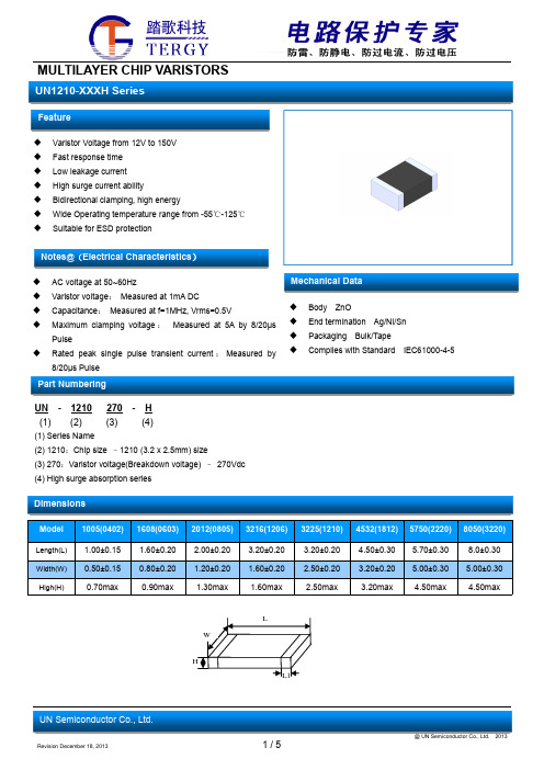
The specimen should be subjected to -40℃, without load for 1000 hours and then Low Temperature Storage stored at room temperature for one two hours. The change of varistor voltage shall be
Pulse Rated peak single pulse transient current : Measured by
8/20µs Pulse
Part Numbering
Mechanical Data
Body ZnO End termination Ag/Ni/Sn Packaging Bulk/Tape Complies with Standard IEC61000-4-5
B0
K0
±0.10 ±0.10
1.88 1.04
T ±0.05 0.22
T2
D0
±0.05 +0.10
0.87 1.50
D1 ±0.05
1.00
P1
P2
±0.10 ±0.05
4.00 2.00
P0 ±0.05
4.00
W ±0.20 8.00
VB
12
10-14
18
15.5-21
21
19-23
24
22-27
27
24-30
30
27-33
33
29-36
37
32-39
39
35-43
47
42-52
53
47-58.5
56
AS-12系列产品性能参数
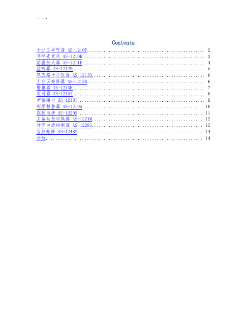
Contents十分区寻呼器 AS-1210P (2)寻呼麦克风 AS-1210R (3)前置放大器 AS-1211P (4)监听器 AS-1212M (5)双五路十分区器 AS-1213B (6)十分区矩阵器 AS-1213D (6)警报器 AS-1215E (7)定时器 AS-1216T (8)市话接口 AS-1218I (9)邻层报警器 AS-1219A (10)强插电源 AS-1220S (11)主备功放切换器 AS-1221M (12)时序电源控制器 AS-1228S (13)音频矩阵 AS-1248S (14)功放 (14)十分区寻呼器 AS-1210P性能特点(1)10分区寻呼报警功能(2)音频信号采用优质平衡传输连接技术(3)音频信号、控制信号采用双绞线同缆实时传输连接技术(4)采用专业级钟声提示音音效电路技术(5)具有四级优先权设计,分别为:本机MIC 1、钟声提示音为最高优先级,紧急音频信号(EMC)为第二级,寻呼麦克风1(MIC1)为第三级,寻呼麦克风2、3、4 (RMIC 2、3、4)和线路(AUX)为第四级(6)采用地址拨码,同时最多8台分区寻呼器相连接(7)15针电脑激活接口,低电平报警激活设备型号AS-1210P报警信号输入口EMC : 10K ohms(Ω) 330mV,不平衡线路输入口LINE :10K ohms(Ω) 330mV,不平衡话筒输入口MIC : 600 ohms(Ω) 5mV,不平衡寻呼话筒输入口四组RMIC1、RMIC2、RMIC3、RMIC4 10k ohms(Ω) 10V,平衡线路输出四组RMIC1、RMIC2、RMIC3、RMIC4 10k ohms(Ω) 10V,平衡非线性失真THD < 0.01% at 1k Hz信号噪声比S/N >70 dB可控制分区数十分区 "CH1~CH10"分区输出控制可手动选择或由警报信号激活任意分区警报激活输入口(0V) 短路信号 15针"ALARM IN (CH1~CH10) 一组警报激活输出口(0V) 短路信号 15针"ALARM OUT (CH1~CH10) 一组警报激活输出口(0V) 短路信号 "ALARM OUT" 二路默音抑制能力本机MIC、钟声提示音为最高优先级。
SOCAY硕凯SC1210ML系列片式压敏电阻型号
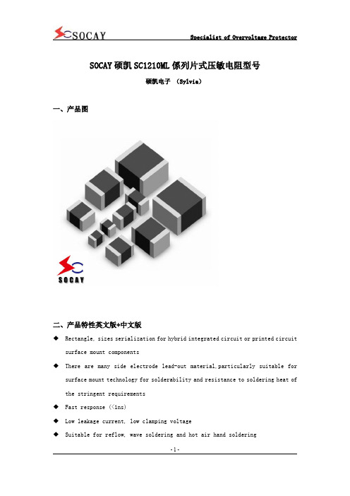
SOCAY硕凯SC1210ML係列片式压敏电阻型号硕凯电子(Sylvia)一、产品图二、产品特性英文版+中文版◆Rectangle,sizes serialization for hybrid integrated circuit or printed circuitsurface mount components◆There are many side electrode lead-out material,particularly suitable forsurface mount technology for solderability and resistance to soldering heat of the stringent requirements◆Fast response(<1ns)◆Low leakage current,low clamping voltage◆Suitable for reflow,wave soldering and hot air hand soldering1、矩形大小的係列化適合於混合集成電路或印製電路板表麵貼裝組件2、有許多側電極管線材料,特別適合嚴格要求的可焊性和抗焊錫熱表麵貼裝技術3、快速反應(<1ns)4、低漏電流,低鉗位電壓5、適合流回,波焊錫和熱空氣的手焊錫三、产品型号SC1210ML180K,SC1210ML240K,SC1210ML270K,SC1210ML330K,SC1210ML390K,SC1210ML470K,SC1210ML560K,SC1210ML680K,SC1210ML101K。
四、产品应用1、應用於主板,筆記本電腦,手機,掌上電腦,手持設備,DSC,DV,掃描儀以及機頂盒等。
2、適合按鈕,電源線和低頻單線路的過電壓保護。
五、等效线路图。
MAXIM MAX11500 数据手册
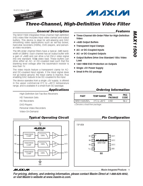
General Description The MAX11500 integrated three-channel high-definition (HD) video filter includes input video clamps and output buffers. This device is ideal for anti-aliasing and DAC smoothing video applications such as set-top boxes, hard-disk recorders (HDRs), DVD players, and person-al video recorders.The 6th-order channel filters have a typical -3dB band-width of 33MHz. Each channel has an output buffer with a gain of +6dB and can drive a full 2V P-P video signal into one standard 150Ωvideo load. These buffers can drive either an AC- or DC-coupled load such that the blanking level voltage after the backmatch resistor is less than 1V.The video inputs feature a transparent clamp for AC-and DC-coupled input signals. If the input signal does not go below ground, the input clamp is inactive, thus enabling DAC outputs to be DC-coupled to the input. The device operates from a single +5V supply, is offered in the upper commercial 0°C to +85°C temperature range, and is available in a small 8-pin SO package.Applications High-Definition Set-Top Box ReceiversHD Television SetsHD RecordersDVD PlayersPersonal Video RecordersVideo-On-DemandFeatures♦Three-Channel 6th-Order Filter for High-Definition Video♦+6dB Output Buffers♦Transparent Input Clamps♦AC- or DC-Coupled Inputs♦AC- or DC-Coupled Outputs♦Output Buffers Drive One Standard 150ΩVideo Load♦12kV HBM ESD Protection on Outputs♦Single +5V Power Supply♦Small 8-Pin SO packageMAX11500________________________________________________________________Maxim Integrated Products1Pin Configuration Typical Operating CircuitFor pricing, delivery, and ordering information, please contact Maxim Direct at 1-888-629-4642, or visit Maxim’s website at .Ordering Information+Denotes a lead-free package.M A X 11500Three-Channel, High-Definition Video Filter 2_______________________________________________________________________________________ABSOLUTE MAXIMUM RATINGSELECTRICAL CHARACTERISTICSStresses beyond those listed under “Absolute Maximum Ratings” may cause permanent damage to the device. These are stress ratings only, and functional operation of the device at these or any other conditions beyond those indicated in the operational sections of the specifications is not implied. Exposure to absolute maximum rating conditions for extended periods may affect device reliability.V CC to GND..............................................................-0.3V to +6V All other pins to GND......-0.3V to the lower of (V CC + 0.3V) and +6V Continuous Power Dissipation (T A = +70°C)8-Pin SO (derate 5.9mW/°C above +70°C)...............470.6mW Maximum Current into any Pin Except V CC and GND......±50mAOperating Temperature RangeMAX11500USA...................................................0°C to +85°C Storage Temperature Range.............................-65°C to +150°C Lead Temperature (soldering, 10s).................................+300°C Junction Temperature......................................................+150°CMAX11500Three-Channel, High-Definition Video Filter_______________________________________________________________________________________3MAGNITUDE RESPONSE (PASSBAND AND STOPBAND)M A X 11500 t o c 01FREQUENCY (MHz)R E S P O N S E (d B )101-60-40-20020-800.1100MAGNITUDE RESPONSE(PASSBAND)M A X 11500 t o c 02FREQUENCY (MHz)R E S P O N S E (d B )1014.55.05.56.06.57.07.58.04.00.1100GROUP DELAYM A X 11500 t o c 03FREQUENCY (MHz)D E L A Y (n s )10110203040506000.11002T RESPONSEMAX11500 toc0440ns/div 200mV/div 200mV/div HD MULTIBURST RESPONSE(1MHz–10MHz)MAX11500 toc054µs/div 200mV/div 200mV/div HD MULTIBURST RESPONSE(20MHz–30MHz)MAX11500 toc064µs/div200mV/div200mV/divTypical Operating Characteristics(V CC = +5V, outputs AC-coupled with 220µF, R LOAD = 150Ωto GND, C IN = 0.1µF, T A = +25°C. All frequency response is relative to 100kHz.)Detailed DescriptionThe MAX11500 integrates three high-definition (HD)video filters, each with a transparent input clamp, a 6th-order lowpass filter with a -3dB bandwidth of 33MHz,and an output stage with a gain of 2V/V. The output sig-nal is offset by typically 550mV to optimize driver per-formance.V OUT = 2 x V IN + 0.55VTypical voltage waveforms are shown in Figures 1 and 2.Transparent ClampsAll inputs feature a transparent clamp that allows either AC- or DC-coupling of the inputs. The clamp remains inactive while the input signal is above ground, offering true DC input coupling. If the signal goes below ground, as is the case if it is AC-coupled, the clamp sets the sync tip close to the ground level.Input CouplingThe choice to AC- or DC-couple the input depends on the video source. Many DACs have a current output and are terminated to ground with a resistor; such sig-nals can be conveniently DC-coupled. In cases where the DC level of the video signal is unknown or outside of the specified input range of the MAX11500, such sig-nals require AC-coupling. Examples of the latter are SCART inputs and DACs terminated to V CC .DC-Coupled InputsIf the input is DC-coupled, the voltage must remain above zero but not exceed the maximum input voltage of 1.7V (typical).Figure 1. Typical AC-Coupled SignalM A X 11500Three-Channel, High-Definition Video Filter 4_______________________________________________________________________________________AC-Coupled InputsIf the input is AC-coupled, the transparent clamp will be active and sets the sync tip or the lowest voltage of the signal close to ground. This clamping behavior is appropriate for unipolar signals such as Y, R, G, or B with or without sync pulse (Figure 3).For bipolar signals such as Pb, Pr signals, the AC-coupled inputs should be biased to a fixed DC voltage to ensure that the transparent clamp never turns on. A suitable network that biases the input to typically 0.59V is shown in Figure 4. The device has an input leakage current (I L ) of typically 0.5µA and thus the bias voltage is derived as follows:HD FiltersThe internal filters are optimized to deliver a flat pass-band along with high stopband attenuation. The filter characteristic has been chosen to provide an excellent time-domain response with low overshoot. The typical -3dB frequency of 33MHz guarantees low attenuation in the passband, while at the same time allowing for a typical attenuation of -48dB at 74.25MHz.V R R R V I x R B CC L( )=+−2121MAX11500Three-Channel, High-Definition Video Filter_______________________________________________________________________________________5Figure 4. AC-Coupling for Bipolar Signals (Pb, Pr)M A X 11500Three-Channel, High-Definition Video Filter 6_______________________________________________________________________________________Output BufferThe MAX11500 features output buffers with +6dB gain that drive a standard 150Ωvideo load. A typical load consists of a 75Ωbackmatch resistor, an optional 220µF or larger coupling capacitor, and a 75Ωtermina-tion resistor. The offset between input and output sig-nals has been chosen such that the blanking level on the output is less than 1V after the backmatch resistor,thus meeting digital TV specifications. This allows the MAX11500 to drive video loads directly without using costly AC-coupling capacitors.Applications InformationOutput ConsiderationsThe MAX11500 outputs can be DC- or AC-coupled.The MAX11500, with +6dB gain, is typically connected to a 75Ωseries backmatch resistor followed by the video cable. If an AC connection is used, choose an AC-coupling capacitor value that ensures that the low-est frequency content in the video signal is passed and the field-time distortion is kept within desired limits. The selection of this value is a function of the input imped-ance and more importantly the input leakage of the cir-cuit being driven. Common industry practice is to use a 220µF or larger capacitor.The outputs of the MAX11500 are fully protected against a short circuit either to the ground or the posi-tive supply of the device. The short-circuit protection circuitry limits the output current to typically 75mA per output. Shorting more than one output simultaneously may exceed the maximum package power dissipation.PCB Layout RecommendationsThe device is thermally designed to operate with mini-mum copper. However, to help with heat dissipation,connect the power and ground traces to large copper areas if possible. Bypass V CC to GND with a 0.1µF capacitor and an additional 1µF capacitor in parallel for additional low-frequency decoupling. Using surface-mount capacitors reduces lead inductance and ensures that the impedance of the capacitors is low over a broad range of frequencies.Place traces carrying video signals appropriately to avoid mutual coupling. If AC-coupling the inputs, place the input coupling capacitors as close as possible to the device and keep traces short to minimize parasitic capacitance and inductance. Doing so extends the performance to the uppermost frequency range possi-ble with the MAX11500.For a recommended PCB layout, refer to the MAX11500EV kit data sheet.MAX11500Three-Channel, High-Definition Video Filter_______________________________________________________________________________________7Typical Operating CircuitM A X 11500Three-Channel, High-Definition Video Filter Maxim cannot assume responsibility for use of any circuitry other than circuitry entirely embodied in a Maxim product. No circuit patent licenses are implied. Maxim reserves the right to change the circuitry and specifications without notice at any time.8_____________________Maxim Integrated Products, 120 San Gabriel Drive, Sunnyvale, CA 94086 408-737-7600©2008 Maxim Integrated Productsis a registered trademark of Maxim Integrated Products, Inc.Package Information(The package drawing(s) in this data sheet may not reflect the most current specifications. For the latest package outline information,go to /packages .)。
MXD1210EWE资料

For free samples & the latest literature: , or phone 1-800-998-8800_______________General DescriptionThe MXD1210 nonvolatile RAM controller is a very low-power CMOS circuit that converts standard (volatile)CMOS RAM into nonvolatile memory. It also continually monitors the power supply to provide RAM write protec-tion when power to the RAM is in a marginal (out-of-tolerance) condition. When the power supply begins to fail, the RAM is write protected, and the device switch-es to battery-backup mode.ApplicationsµP Systems ComputersEmbedded Systems____________________________Featureso Battery Backupo Memory Write Protectiono 230µA Operating-Mode Quiescent Current o 2nA Backup-Mode Quiescent Current o Battery Freshness Seal o Optional Redundant Batteryo Low Forward-Voltage Drop on V CC Supply Switch o 5% or 10% Power-Fail Detection Options o Tests Battery Condition During Power-Up o 8-Pin SO Available______________Ordering Information*Contact factory for dice specifications.MXD1210Nonvolatile RAM Controller________________________________________________________________Maxim Integrated Products 1__________Typical Operating Circuit19-0154; Rev 1; 3/96PARTTEMP. RANGE PIN-PACKAGE MXD1210CPA 8 Plastic DIP MXD1210CSA 8 SOMXD1210CWE 0°C to +70°C 16 Wide SO 0°C to +70°C 0°C to +70°C MXD1210C/D Dice*MXD1210ESA -40°C to +85°C 8 SOMXD1210EPA -40°C to +85°C 8 Plastic DIP MXD1210EWE -40°C to +85°C 16 Wide SO MXD1210MJA-55°C to +125°C8 CERDIP0°C to +70°C _________________Pin ConfigurationsM X D 1210Nonvolatile RAM ControllerABSOLUTE MAXIMUM RATINGSELECTRICAL CHARACTERISTICS(T A = T MIN to T MAX , unless otherwise noted.)Stresses beyond those listed under “Absolute Maximum Ratings” may cause permanent damage to the device. These are stress ratings only, and functional operation of the device at these or any other conditions beyond those indicated in the operational sections of the specifications is not implied. Exposure to absolute maximum rating conditions for extended periods may affect device reliability.ELECTRICAL CHARACTERISTICS(V CCI = +4.75V to +5.5V, TOL = GND; or V CCI = +4.5V to +5.5V, TOL = V CCO ; T A = T MIN to T MAX ; unless otherwise noted.)V CCI to GND ................................................................-0.3V, +7V VBATT1 to GND..........................................................-0.3V, +7V VBATT2 to GND.......................................................... -0.3V, +7V V CCO to GND..................................................... -0.3V, V S + 0.3V(V S = greater of V CCI , VBATT1, VBATT2)Digital Input and Output Voltages to GND............. 0.3V, V CCI + 0.3VContinuous Power Dissipation (T A = +70°C)8-Pin Plastic DIP (derate 9.09mW/°C above +70°C)....727mW 8-Pin SO (derate 5.88mW/°C above +70°C).................471mW 16-Pin Wide SO (derate 9.52mW/°C above +70°C)......762mW 8-Pin CERDIP (derate 8.00mW/°C above +70°C).........640mW Operating Temperature RangesMXD1210C_ _..................................................... 0°C to +70°C MXD1210E_ _.................................................. -40°C to +85°C MXD1210MJA................................................ -55°C to +125°C Storage Temperature Range ........................... -65°C to +150°C Lead Temperature (soldering, 10sec)............................ +300°CNonvolatile RAM ControllerELECTRICAL CHARACTERISTICS(V CCI < VBATT; positive edge rate at VBATT1, VBATT2 > 0.1V/µs, T A = T MIN to T MAX ; unless otherwise noted.)MXD1210ELECTRICAL CHARACTERISTICS(T A = T MIN to T MAX , unless otherwise noted.)_______________________________________________________________________________________3V CC POWER TIMING CHARACTERISTICS(V= +4.75V to +5.5V, TOL = GND; or V = +4.5V to +5.5V, TOL = V ; T = T to T ; unless otherwise noted.)TIMING CHARACTERISTICS(V CCI < +4.75V to +5.5V, TOL = GND; or V CCI < +4.5V , TOL = V CCO ; T A = T MIN to T MAX ; unless otherwise noted.)Note 1:Only one battery input is required. Unused battery inputs must be grounded.Note 2:I CCO1is the maximum average load current the MXD1210 can supply to the memories.Note 3:I CCO2is the maximum average load current the MXD1210 can supply to the memories in battery-backup mode.Note 4:CEO can sustain leakage current only in battery-backup mode.Note 5:Guaranteed by design.Note 6:t CE max must be met to ensure data integrity on power loss.M X D 1210Nonvolatile RAM Controller 4_____________________________________________________________________________________________________________________________________________________Pin DescriptionFigure 1. Block Diagram______________Detailed DescriptionMain FunctionsThe MXD1210 executes five main functions to perform reliable RAM operation and battery backup (see Typical Operating Circuit and Figure 1):1. RAM Power-Supply Switch: The switch directs power to the RAM from the incoming supply or from the selected battery, whichever is at thegreater voltage. The switch control uses the same criterion to direct power to MXD1210 internal circuitry.2. Power-Failure Detection: The write-protection func-tion is enabled when a power failure is detected.The power-failure detection range depends on the state of the TOL pin as follows:Power-failure detection is independent of the battery-backup function and precedes it sequentially as the power-supply voltage drops during a typical power failure.3. Write Protection: This holds the chip-enable output (CEO ) to within 0.2V of V CCI or of the selected bat-tery, whichever is greater. If the chip-enable input (CE )is low (active) when power failure is detected,then CEO is held low until CE is brought high, at which time CEO is gated high for the duration of the power failure. The preceding sequence com-pletes the current RD/WR cycle, preventing data corruption if the RAM access is a WR cycle.4. Battery Redundancy: A second battery is optional.When two batteries are connected, the stronger battery is selected to provide RAM backup and to power the MXD1210. The battery-selection circuitry remains active while in the battery-backup mode,selecting the stronger battery and isolating the weaker one. The battery-selection activity is trans-parent to the user and the system. If only one bat-tery is connected, the second battery input should be grounded.5. Battery-Status Warning: This notifies the system when the stronger of the two batteries measures ≤2.0V. Each time the MXD1210 is repowered(V CCI > V CCTP ) after detecting a power failure, the battery voltage is measured. If the battery in use is low, following the MXD1210 recovery period, the device issues a warning to the system by inhibit-ing the second memory cycle. The sequence is as follows:First access: read memory location n, loc(n) = x Second access: write memory location n,loc (n) = complement (x)Third access: read memory location n, loc (n) = ?If the third access (read) is complement (x), then the battery is good; otherwise, the battery is not good.Return to loc(n) = x following the test sequence.Freshness-Seal ModeThe freshness-seal mode relates to battery longevity during storage rather than directly to battery backup.This mode is activated when the first battery is connect-ed, and is defeated when the voltage at V CCI first exceeds V CCTP . In the freshness-seal mode, both bat-teries are isolated from the system; that is, no current is drained from either battery, and the RAM is not pow-ered by either battery. This means that batteries can be installed and the system can be held in inventory with-out battery discharge. The positive edge rate at VBATT1 and VBATT2 should exceed 0.1V/µs. The bat-teries will maintain their full shelf-life while installed in the system.Battery BackupThe Typical Operating Circuit shows the MXD1210 con-nected in order to write protect the RAM when V CC is less than 4.75V, and to provide battery backup to the supply.MXD1210Nonvolatile RAM Controller_______________________________________________________________________________________5CONDITION V CCTP RANGE (V)TOL = GND 4.75 to 4.50TOL = V CCO4.50 to 4.25M X D 1210Nonvolatile RAM Controller 6_______________________________________________________________________________________Figure 2. Power-Up Timing Diagram Figure 3. Power-Down Timing DiagramMXD1210Nonvolatile RAM Controller_______________________________________________________________________________________7__________________Chip TopographyTRANSISTOR COUNT: 1436;LEAVE SUBSTRATE UNCONNECTED.VBATT2CECEO V CCO VBATT1TOLV CCIGND0.121" (3.073mm)0.080" (2.032mm)Maxim cannot assume responsibility for use of any circuitry other than circuitry entirely embodied in a Maxim product. No circuit patent licenses are implied. Maxim reserves the right to change the circuitry and specifications without notice at any time.8____________________Maxim Integrated Products, 120 San Gabriel Drive, Sunnyvale, CA 94086 (408) 737-7600©1996 Maxim Integrated ProductsPrinted USAis a registered trademark of Maxim Integrated Products.M X D 1210Nonvolatile RAM Controller ________________________________________________________Package Information。
AD2S1210器件手册_简中
—C—S—下降沿到—R—D—下降沿滞后
配置模式下—R—D—低到数据可用的使能滞后
VDRIVE=4.5V至 5.25V
VDRIVE=2.7V至 3.6V
VDRIVE=2.3V至 2.7V
———
———
RD上升沿到CS 上升沿
———
RD高到数据高阻的禁能滞后
———
CS 高到数据高阻的禁能滞后
—R—D—上升沿到W— —R— /—F—S—Y—N——C—下降沿滞后
电源要求
AVDD
4.75
最大
0.9 3.1 9.0 40
2.2 6.0 14.7 66 4.0 2.53 20 30 100
2.53
0.8
0.8 0.7
10 80
0.4
10
5.25
单位
ms ms ms ms
工况/备注
调整至±2LSB 内,CLKIN = 8.192 MHz 调整至±2LSB 内,CLKIN = 8.192 MHz 调整至±2LSB 内,CLKIN = 8.192 MHz 调整至±2LSB 内,CLKIN = 8.192 MHz
16 位并行接口、4 线串行接口和带方向输出的标准 AB 正交增量编码器拟真。 6. 数字速度输出。16 位并口或 4 线串口都可读取 10 位~16 位带符号数字速度。
规格
AVDD = DVDD = 5.0 V ± 5%, CLKIN = 8.192 MHz ± 25%, EXC, E——X—C—频率 = 10 kHz至 20 kHz (10 位); 6 kHz至 20 kHz (12 位); 3 kHz至 12 kHz (14 位); 2 kHz至 10 kHz (16 位); TA = TMIN至 TMAX; 除非另外指明。1 表 1.
msc1210中文
参数
模拟输入 AIN0-AIN7 AINCOM 模拟输入范
围
全输入电压范围 差分输入阻抗
输入电流 带宽
快速沉积滤波器 Sinc2滤波器 Sinc2滤波器
可编程增益放大器 输入电容 输入漏电流 熔断电流
偏移DAC 偏移DAC范围 偏移DAC单调性 偏移DAC增益偏差 偏移DAC增益偏差漂移
条件
缓冲区关闭 缓冲区打开 IN+ - IN- 看图4 缓冲区关闭 缓冲区打开
256
内部 MOVX 静态随机存储器 字节 1024
1024
1024
1024
数
外部可存取存储器 字节数
程序 64K 数据 64K
程序 64K 数据 64K
程序 64K 数据 64K
程序 64K 数据 64K
注释 1 所有器件的外围特性相同 仅闪存容量不同 2 类型号的最后一位数字代表片内闪存容量 的大小= 2N KB
DC下 fCM = 60Hz, fDATA = 10Hz fCM = 50Hz, fDATA = 50Hz fCM = 60Hz, fDATA = 60Hz fSIG = 50Hz, fDATA = 50Hz fSIG = 60Hz, fDATA = 60Hz
DC下 dB =–20log( VOUT/ VDD)
MSC1210YX
最小值
典型值
最大值
单位
AGND-0.1 AGND
1
5/PGA 0.5
AVDD+0.1
AVDD-1.5
+VREF/PGA
0.469 • fDATA 0.318 • fDATA 0.262 • fDATA
9 0.5 +6
128
ioLogik E1200 Series (E1210) 固件发布说明书

Firmware for ioLogik E1200 Series (E1210) Release NotesSupported Operating SystemsNotesChangesApplicable ProductsBugs Fixed• Added SNMP Trap Community Setting to the web console.• Added a note on the password settings page that passwords are limited to 16 characters.• Fixed DHCP lease time did not ask for extension when half of the lease time elapsed.• Closed IP forwarding function (Port 0).• Closed UDP Port 161 when SNMP agent is disabled.• Fixed RESTful API header case-sensitive issue.• Fixed invalid token issue on login page when using Firefox.EnhancementsN/AioLogik E1210-T, ioLogik E1210• Added OPTIONS method for RESTful API.• Added quick access URI for RESTful API.New FeaturesN/A• This version of the firmware only works with ioSearch v2.0 or later versions.• To prevent system failure, only update the next or the previous released firmware version to prevent from system failure.Supported Operating SystemsNotesChangesApplicable ProductsBugs FixedN/A• Fixed file transfer problems when using the Chrome browser (e.g., firmware update, configuration import or export).EnhancementsN/AioLogik E1210, ioLogik E1210-T• Added the EtherNet/IP protocol.• Added RESTful API.• Added new registers for the Modbus/TCP protocol.• Added new OIDs for the SNMP protocol.• Modbus, EtherNet/IP, and RESTful services can be disabled (enabled by default).• Added sending heartbeat to port 9500 of MX-AOPC UA Server after the heartbeat function is enabled.• Increased password length from 8 to 16 characters.• Added a function to check special characters to prevent Cross-Site Scripting.• Passwords are now sent using the POST method instead of the GET method.New FeaturesN/AN/ASupported Operating SystemsNotesChangesApplicable ProductsBugs FixedN/AN/AEnhancementsN/AioLogik E1210, ioLogik E1210-T• Improved protocol efficiency for the ioLogik 2500 Series.New FeaturesN/AN/ASupported Operating SystemsNotesChangesApplicable ProductsBugs FixedN/A• Unable to disable the P2P heartbeat interval.• When the P2P client heartbeat is larger than 256 the time interval is incorrect.EnhancementsN/AioLogik E1210, ioLogik E1210-T• Supports ioLogik 2500 expansion mode.• Supports setting an initial value for a counter.New FeaturesN/AN/ASupported Operating SystemsNotesChangesApplicable ProductsBugs FixedN/A• The counter storage is deleted when the power fails.EnhancementsN/AioLogik E1210-T, ioLogik E1210• Supports SNMP protocol.• Added P2P heartbeat function.New FeaturesN/A• This version of firmware only works with ioSearch v1.5 or later versions.• Use the web console when upgrading the firmware from v1.0 to v1.10.Supported Operating SystemsNotesChangesApplicable ProductsBugs Fixed• Ensured that the system works properly after unstable power conditions.N/AEnhancementsN/AioLogik E1210, ioLogik E1210-TN/ANew FeaturesN/AN/ASupported Operating SystemsNotesChangesApplicable ProductsBugs Fixed• Improved firmware upgrading speed.• Removed Modbus/TCP ID checking mechanism.N/AEnhancementsN/AioLogik E1210, ioLogik E1210-T• Added "Locating I/O" function in General Settings.• Added Modbus address function code=0x08 for “ECHO” function.• Counter overflow status displayed in Channel Settings can be cleared manually.New FeaturesN/A• This version of the firmware only works with ioSearch v1.5 or later versions.• Use the web console when upgrading the firmware from v1.0 to v1.9.。
mx1210p 高性能多模式pwm控制器数据手册说明书

GENERAL DESCRIPITIONMX1210P is a highly integrated current mode PWM controller, optimized for high performance, low standby power consumption and wide output voltage range PD adapter solutions. The circuit is as well compatible with cost effective offline flyback converter applications covering a wide output range.At full loading, the IC operates in fixed frequency mode. When the loading goes low, it operates in Green mode with valley switching for high power conversion efficiency can be achieved in the whole loading range.MX1210P offers complete protection coverage including cycle-by-cycle current limiting (OCP), overload protection (OLP), over temperature protection (OTP), output short current protection (SCP), output and VDD over voltage protection (OVP & VDD OVP). Excellent EMI performance is achieved with MAXIN proprietary frequency shuffling technique. The tone energy at below 22kHz is minimized to avoid audio noise during operation. MX1210P is offered in SOT23-6 package.ApplicationsBattery chargers PD adaptersWide output range adapters Motor adapterTypical ApplicationFEATURES♦ Multi-Mode Operation●65kHz fixed frequency mode @ Full Load ●130kHz@Peak load in 40ms●Valley switching operation @ Green mode●Burst Mode @ Light Load and No Load♦Adaptive loop gain compensation with Iovp current detection ♦Ultra low operation current at light and no load ♦Internal OCP compensation for universal line voltage ♦Extend burst mode control for improved efficiency and lowstandby power♦Power on soft start reducing MOSFET VDS stress ♦Frequency shuffling for EMI ♦Audio noise free operation ♦Comprehensive protection coverage●VDD under voltage lockout with hysteresis (UVLO) ●Cycle-by-cycle over current protection (OCP) with autorecovery●External over temperature protection (EXT_OTP) ●VDD over voltage protection ●Output over voltage protection●Output short current protection (SCP) with autorecovery●Brownout protection with auto recovery ●Output diode short protection with auto recoveryGND 1DMAG 3FB 2CS4VDD 5GATE 6MX1210PGNDLNGeneral informationOrdering informationPart Number DescriptionMX1210P SOT23-6,Halogen-free,RoHS Package dissipation ratingPackage RθJA(℃/W)SOT23-6200Absolute maximum ratingsParameter ValueVDD DC supply voltage60VFB input voltage-0.3 to 7VCS input voltage-0.3 to 7VDMAG input voltage-0.3 to 7VJunction temperature T J-40 to 150℃Ambient temperature T A-40 to 85℃Storage temperature T STG-55 to 150℃ESD(HBM)±2.0kVLeading temperature(soldering, 10secs)260℃Note: stresses beyond those listed under “absolute maximum ratings” may cause permanent damage to the device. These are stress ratings only, functional operation of the device at these or any other conditions beyond those indicated under “recommended operating conditions” is not implied. Exposure to absolute maximum rated conditions for extended periods may affect device reliability.Marking information Recommended operating conditionSymbol Parameter Range VDD VDD supply voltage10-48V PD Power dissipation @TA=25℃0.59W Terminal assignments1210PGNDFBDMAG CSVDDGATEPINNO.PINnameDescription1GND Ground pin.2FBFeedback input pin. The PWM dutycycle is determined by voltage levelinto this pin and current-sense signalCS pin.3DMAGDemagnetization input. Input andoutput voltages are sensed from theauxiliary winding.4CSCurrent sense pin, connect resistors toground.5VDD Power supply.6GATE Gate driver for external MOSFET.MX1210 YYWW1210X YY WWPWM Controller Package Year code Week codeT/E:SOT23-621:year 202122:year 2022Week code01-52Block DiagramVDDVREF IREFUVLOOVPHVOVPAVDDInternal blocksGNDShort Current Protection External OTPExternal OVPTEMP SenseValley DetectIovp DetectDMAGO V /O T PD i o S TOTPOVPS C POV/OTPValleyPeak Load Green/BurstOscillatorS SRValleyQLogic controlSoft driverO L PO C PAll PRTDemagSample LEB Slope CompensationGmCC loopPWM comparatorPK detect comparatorTimerOLP AVDDDio STVth_PKGATECSFBElectrical characteristics(TA=25℃,VDD=18V,unless otherwise noted)Symbol Parameter Test condition Min Typ.Max Unit VDD supply voltageI startup VDD startup current VDD=UVLO_OFF-1V 2.010.0μAI_VDD VDD normal operation current V FB=3V1 2.0 2.5mA I_ Burst Burst mode operation current VFB=0.5V0.360.45mA UVLO_ON VDD under voltage lockout enter 6.77.27.7V UVLO_OFF VDD under voltage lockout exit15.216.217.2VV_Pull/up Pull-up PMOS active10VV DD_OVP Over voltage protection voltage FB=3V, VDD ramp up until gateclock is off50.052.054.0VT_recovery Restart time for auto-recovery protection Other protection 1.4s FB pin – Feedback input sectionV FB_Open FB open loop voltage 5.1VAvcs PWM input gain ΔVFB/ΔVCS VDMAG>1.25V 3.5V/V VDMAG<1.25V 4.5V/VD_MAX Max duty cycle @ VDD=18V, VFB=3V,VCS=0.3V7090%I FB_short FB pin short circuit current Current for short FB to GND250μA V FB_green The threshold enters green mode 2.05V V REF_burst_H The threshold exits burst mode 1.2V V REF_burst_L The threshold enters burst mode 1.1V V FB_OLP Over load protection 4.75 5.5V T D_OLP Over load debounce time13s T D_PK Peak load debounce time40ms R FB_IN Input impedance20kΩCS pin – Current sense inputT CS _SST Soft start time of CS threshold 4.0ms T_blanking Leading edge blanking time300nsT D_OC Over current detection and delay From over current occurs till gatedriver turns off90nsV CS_PK Internal current limiting threshold voltagewith zero duty cycle0.4940.5000.506VV CS_PKclamp CS voltage clamper0.715VV CS_SRST Secondary rectifier diode short protectionthreshold voltage1.1 1.2 1.3VV CS_EXOTP External OTP threshold voltage DMAG=1.8V0.80V T D_EXOTP External OTP delay time424956msOscillatorF OSC_NOM Normal frequency of high output voltage VDD=18V, FB=3V,DMAG加-114uA,CS=3.3V616569kHzF OSC_PK Peak load frequency FB=3V130kHz F OSC_JT Frequency jittering-7+7% F OSC_shuffling Shuffling frequency240Hz F OSC_TEMP Frequency temperature stability 1.0% F OSC_VDD Frequency VDD voltage stability 1.0% F OSC_burst Burst mode frequency22kHz Gate driverV GL Gate low voltage @ VDD=15V, Io=20mA 1.0VV GH Gate high voltage @ VDD=15V,Io=20mA8.0VV G_clamping Gate clamp voltage11.5VT_rise Gate voltage rising time 1.2V ~ 10.8V @CL=1000pF240nsT_fall Gate voltage falling time 10.8V ~ 1.2V @CL=1000pF25nsDMAG pinV TH_OVP Output over voltage protection thresholdvoltage3.50 3.60 3.70VV TH_UVP Output under-voltage protection thresholdvoltage0.300.350.40VT D_UVP Output under voltage protection delaytime91215msT BLK_LL Blanking time of DMAG pin @ light load V FB<2.05V 1.7μs T BLK_HL Blanking time of DMAG pin @ high load V FB>2.05V 2.3μs I DMAG_BNI Brown in protection threshold current115130145μA I DMAG_BNO Brown out protection threshold current120135150μA T D_BNO Brown out protection delay time FOSC=83KHz424956ms I DMAG_HVHYS Hysteresis of high VIN entry7.5μA I DMAG_MAX Maximum DMAG sourcing current1000μA Internal OTPOTP_in155℃Characteristic plots VDD=18VOperation descriptionMX1210P is a highly integrated current mode PWM controller, optimized for high performance, low standby power consumption and wide output voltage range PD adapter solutions. Together with PD secondary controller. The power circuit is as well compatible with cost effective offline flyback converter applications covering a wide output range. The extended burst mode control greatly reduces the standby power consumption and helps the design easily to meet the international power conservation requirements. Startup and Internal under voltage lockoutStartup current of MX1210P is designed to be very low so that VDD could be charged up to UVLO_OFF threshold level and device starts up quickly. A large value startup resistor can therefore be used to minimize the power loss yet achieve a reliable startup in application.To optimize power efficiency, startup resistors can be added to the AC line, which not only can reduce power loss but can reset latched mode protections faster.VDDVDD current UVLO_OFF UVLO_ON16.5V7.2VI startupI_VDDttFig1 startup current timingOperation currentThe typical operating current of MX1210P is 2mA. Good efficiency is achieved with this low operating current together with the extended burst mode control features. Soft startMX1210P features an internal 4ms soft start to soften the electrical stress occurring in the power supply during startup. It is activated during the power in sequence. As soon as VDD reaches UVLO_OFF, the CS peak voltage is gradually increased from 0V to the maximum level. Every restart up begins with a soft start.Adaptive loop gain compensationWith MAXIN proprietary technology, an adaptive loopcompensation is implemented to ensure the system loop stability for wide output voltage range according to I_OVP current detection.Frequency shuffling for EMI improvementThe frequency shuffling is implemented in MX1210P. The oscillation frequency is modulated so that the tone energy is spread out. The spread spectrum minimizes the system design. Extended burst mode operationAt light load or no-load condition, most of the power dissipation in a switching mode power supply is from switching loss of the MOSFET, the core loss of the transformer and the loss of the snubber circuit. The magnitude of power loss is in proportion to the switching frequency. Lower switching frequency leads to the reduction on the power loss and thus conserves the energy.The switching frequency is internally adjusted at light load or no-load condition. The switching frequency reduces at light load or no load to improve the conversion efficiency. At light load or no-load condition, the FB input drops below V REF_burst_L and system enters burst mode. The gate drive output switches when FB input rise back to V REF_burst_H . Otherwise the gate drive remains at off state to minimize the switching loss and reduces the standby power consumption tothe greatest extend. Oscillator operationDuring the full load power operation, MX1210P operates at 65kHz fixed frequency of high output voltage (V FB >2.05V typical ). The efficiency and system cost are controlled at anoptimal level. At light load, MX1210P enters the light load mode, where the output current is reduced. The switching losses are reduced by lowering the switching frequency.FOSCFB65kHz22kHzV BURST V GREEN V FULL 130kHzV PEAKV OLPFig2 FB voltage vs frequencyCurrent sensing and leading-edge blankingCycle by cycle current limiting is offered in MX1210P current mode PWM control. The switch current is detected by a senseresistor into CS pin. At internal leading-edge blanking circuit chops off the sensed voltage spike at initial internal power MOSFET on state due to snubber diode reverse recovery and surge gate current of power MOSFET. The current limiting comparator is disabled and cannot turn off the power MOSFET during the blanking period. The PWM duty cycle is determined by the current sense voltage and the FB voltage. Internal synchronized slope compensationBuilt-in slope compensation circuit adds voltage ramp into the current sense input voltage for PWM generation. This greatly improves the close loop stability at CCM and prevents the sub-harmonic oscillation and thus reduces the output ripple voltage. Demagnetization detectionThe transformer core demagnetization is detected by monitoring the voltage activity on the auxiliary windings. This voltage features a flyback polarity. After the on time, the switch is off and the flyback stoke starts. After the fly-back stroke, the drain voltage shows an oscillation with a frequency of approximately D P C L π1/2 , where L P is the primary inductance of primary winding and C D is the capacitance on the drain node.Drain voltagetTonT Possible valleys for restartsFig3 valley detectionThe typical detection level is fixed at 85mV at the DMAG pin. Demagnetization is recognized by detection of a possible valley when the voltage at DMAG pin is below 85mV in falling edge.During the power MOSFET on time, the auxiliary winding voltage is negative, and the MX1210P outputs a clamp current to clamp the DMAG voltage at 0V . The MX1210P has built in characteristics, a DMAG brown in protection threshold current I DMAG_BNI (135uA typical) and a DMAG brown out protection threshold I DMAG_BNO , for the DMAG pin. The bulk-capacitor brown in and brown out voltages, V BULK_BNI and V BULK_BNO , can be programmed by adjusting R D1 and R D2 at the DMAG pin, as shown in Figure4. Once the brown in or brown out threshold voltage is set, the other one will be determinedaccordingly. The bulk capacitor brown-out threshold voltage V BULK_BNO can be obtained according to the following equation:DMAG_BNIBULK_BNI DMAG_BNOBULK_BNO I V I V =When the MOSFET turns off, the DMAG pin senses the output voltage of the power stage across the auxiliary winding, with a ratio equal to the turn ratio of the auxiliary and secondary windings, and then scaled with the resistor divider R D2/R D1, as shown in Figure4. The voltage divider and R D1/R D2 can be calculated by the following equation:I R N V N =⋅⋅(For brown out)V R R R N V N =+⋅(For V OUT_OVP )Where the V TH_OVP 3.60V (typical ).DMAGCSGATE NPNSR D2R D1MX1210PV OUTFig4 DMAG pin applicationIn addition, when the MOSFET just turns off, leakage inductance of the transformer and parasitic capacitance of theMOSFET induces resonant oscillations on the DMAG pin. Theresonant oscillations may cause the MX1210P to falsely trigger DMAG over voltage protection, which thus fails to reflect actual output over voltage fault condition so that the circuit may not function properly. As load increases, the duration of the resonant oscillation may also increase. A small bypass capacitor which sized from 15-33pF and placed as close to the DMAG pin as possible is recommended to be added to suppress such noises on the DMAG pin as shown in Figure4. If a larger bypass capacitor may cause the DMAG voltage to be phase shifted too much for the MOSFET not be switched on at exact valley points. Protection controlsGood power supply system reliability is achieved with auto recovery protection features including OCP, output short protection (SCP), Under V oltage Lockout on VDD (UVLO) and peak load protection, and latched shutdown featuresWUXI MAXIN MICRO10 / 13 无锡明芯微电子有限公including Over Temperature Protection, VDD and output Over V oltage Protection (OVP).With MAXIN proprietary technology, the OCP is line voltage compensated to achieve constant output OCP limit over the universal input voltage range and its dependency on primary inductance and frequency is removed.At overload condition when FB pin input voltage exceeds power limit threshold value for more than Td_OLP, control circuit reacts to shut down the converter. It restarts when VDD voltage drops below UVLO limit. For protection with latched shut down mode, control circuit shuts down (latch) the power MOSFET when an over temperature condition or over voltage condition is detected until VDD drops below 4.8V (Latch release voltage ), and the device enters power on restart-up sequence thereafter. Over current protectionMX1210P provides an adaptive cycle-by-cycle OCP compensation method varying with gate on duty cycle in Figure6. The maximum cycle-by-cycle OCP threshold voltage, Vth_PK, is 0.715V .At PWM off state, 100uA current flows out of CS pin to generate a voltage through R1 and Rsense. The final CS peak clamping voltage threshold is adjusted by the added voltage. uA 1001R V V ⋅+=Vth_PK0.715V0.5VD1Figure5 cycle by cycle OCP compensationPin floating and short protectionMX1210P provides pin floating protection for all the pins and pin short protection for adjacent pins. In the cases when a pin is floating or two adjacent pins are shorted, Gate switching is disabled.Programmable external over temperature protection The MX1210P includes programmable external over temperature protection, implemented with a fast diode and a resistive voltage divider, which consists of an external NTC resistor to sense the power system temperature, as shown in figure6. During the MOSFET off time, the auxiliary windingvoltage V AUX is constant, and the CS voltage, sampled as a fraction of the clamped voltage V AUX_CLAMP and compared with the internal reference voltage to set the over temperature protection threshold voltage. When the system temperature gets higher, the resistance of NTC resistor becomes smaller. By adjusting the value of the setting resistor R SET , the threshold temperature for over temperature protection can be programmed. During the MOSFET off time, if the sampled CS voltage exceeds the external OTP threshold voltage V TH_OTP and sustains for the external OTP delay time TD_OTP, the controller will be shut down and the switching will be stopped. If the OTP condition is removed, the controller will automatically resume operation. The design equation for the external OTP threshold voltage is expressed as below: ()SETNTC CS CSP CSCSP OTP _F OUT _F MAX _O S A OTP _TH R R R R R R V -V V N N V ++++⨯⎥⎦⎤⎢⎣⎡+⨯= Where V O_MAX is the maximum normal output voltage, and R NTC is the NTC resistance at the threshold temperature for external OTP . It is highly recommended to use a fast diode (CT ≤5pF and Trr ≤50ns), ex. 1N4148 series, for external OTP application to prevent the CS pin from wrong regulation or being damaged by the negative voltage spikes.DMAGCS GATE MX1210PR SETR NTCV F_OTPNA NSV OV F_OUTR CSR CSPVCCNPV AUXFigure6 external over temperature protection application Feedback resistorsTo enhance efficiency at light load, the power loss caused by the feedback resistors, in parallel with the opto-coupler as shown in Figure7, must be reduced. Since the current through the feedback resistor is very small, a shunt regulator, especially with its minimum regulated current, should be carefully chosen to ensure that the shunt regulator can still regulate theoutput voltage at such a small cathode current.R feedbackFigure7 Feedback resistorDriverThe power MOSFET is driven by a dedicated gate driver for power switch control. Too weak the gate driver strength results in higher conduction and switch loss of MOSFET while too strong gate driver strength results the compromise of EMI.A good tradeoff is achieved through the built-in totem pole gate design with right output strength and dead time control. The low idle loss and good EMI system design is easier to achieve with this dedicated control scheme.Layout considerationsA proper PCB layout can alleviate unknown noise interference and EMI emission in a switch mode power supply. It is recommended to follow the following PCB layout guidelines when a switch mode power supply is to be designed:♦The current path A, starting from the bulk capacitor, through the transformer, the MOSFET, the resistor Rcs and back to the bulk capacitor, is a high frequency and high current loop. This path should be kept as small as possible to decrease noise coupling and kept away from other low voltage traces, such as control paths.♦The path B, starting from the auxiliary winding, through the resistor, the diode, and VDD capacitor to the VDD pin, is also recommended to be as short as possible. Besides, the VDD capacitor should placed as close to the VDD pin as possible.♦The path C, from the RCD snubber circuit to the MOSFET should also be kept short as it is also a loop with high frequency.♦The path D, starting from the second winding, through the rectifier diode, the rectifier capacitor, back to second winding, is also recommended to be as short as possible. In addition, the copper areas at the anode and cathode of the diode must be large enough to ease sinking heat from the diode.♦The path E which is from the GATE pin, through the MOSFET, the current sense resistor and back to the MX1210P ground should be kept as small as possible.♦The ground traces of the bulk capacitor Cg, the current sense resistor Rg,the VDD capacitor CEg, the auxiliary winding Nag, and the power circuit Ug, should be separated to reduce noise, output ripple and EMI emission. The ground traces of the auxiliary winding Na and the MX1210P are connected together at the VDD capacitor ground. Then the connected ground trace goes through the VDD capacitor, the current sense ground, and to the bulk capacitor ground in turn. The area of the bulk capacitor ground trace should be large enough.♦The bypass capacitor should be placed as closed to the power circuit as possible.GND1DMAG3FB2CS4VDD5GATE6MX1210PLNSRPath CPath DPath APath BPath ENagRgCEgUgFBgDMgFigure8 PCB layout guidePackage informatione E1Ee1DA A2A3A1Lθ0.25SYMBOLMILLIMETERS INCHESMIN NOM MAX MIN NOM MAXAA10.040.150.00160.0059 A2 1.00 1.10 1.200.0390.0430.047 A30.550.650.750.0220.0260.029D 2.72 2.92 3.120.1070.1150.123E 2.60 2.80 3.000.1020.1100.118 E1 1.40 1.60 1.800.0550.0630.071 e0.95BSC0.037BSCe1 1.90BSC0.074BSCL0.300.600.0120.024θ08°08°SOT23-6 for MX1210PRestrictions on Product Use◆MAXIN micro is continually working to improve the quality and reliability of its products. Nevertheless, semiconductor devices in general can malfunction or fail due to their inherent electrical sensitivity and vulnerability to physical stress. It is the responsibility of the buyer, when utilizing MAXIN products, to comply with the standards of safety in making a safe design for the entire system, and to avoid situations in which a malfunction or failure of such MAXIN products could cause loss of human life, bodily injury or damage to property.◆In developing your designs, please ensure that MAXIN products are used within specified operating ranges as set forth in the most recent MAXIN products specifications.◆The information contained herein is subject to change without notice.。
cc1150中文
第 - 2 - 页 共 46 页
目录 1 缩写词 ......................................................................................................................................... 2 2 绝对最大等级 ............................................................................................................................. 5 3 工作条件 ..................................................................................................................................... 5 4 电气规范 ..................................................................................................................................... 5 5 常规特性 ..................................................................................................................................... 6 6 RF 传输环节 .............................................................
VJ1210Q1R8DXCAT资料

10000 1000 100 10 1 100 FREQUENCY (MHz) Q vs FREQUENCY - VJ1210, 50V 1000 1000
ESR (Ω)
10pF 0.1 100pF
Q
100pF
0.01 100 FREQUENCY (MHz) ESR vs FREQUENCY - VJ1210, 50V 1 1000
A MARKING
T PACKAGING
VJ = MLCC
0603 0805 1206 1210
Q = High Q
A = Unmarked
Expressed in picofarads (pF). The first two digits are significant, the third is a multiplier. An “R” indicates a decimal point. Examples: 102 = 1000pF. 1R8 = 1.8pF.
ORDERING INFORMATION
VJ PRODUCT SERIES
0805 CASE SIZE
Q DIELECTRIC
102 CAPACITANCE NOMINAL CODE
A K X DC CAPACITANCE TERMINATION VOLTAGE TOLERANCE RATING A = 50V B = 100V C = 200V
X = Nickel barrier with 100% tin plated finish F = Palladium silver
T = 7" Reel, plastic tape C = 7" Reel, paper tape R = 11 1/4" Reel, plastic tape P = 11 1/4" Reel, paper tape B = Bulk NOTE: 0402 and 0603 available in paper tape only
K110中文资料
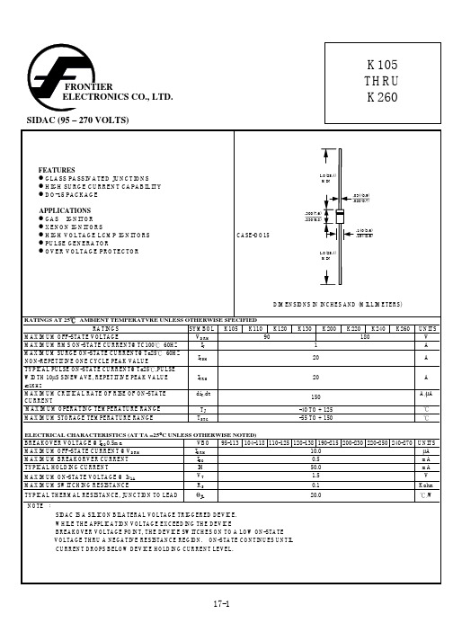
ELECTRICAL CHARACTERISTICS (AT TA =25°C UNLESS OTHERWISE NOTED)
BREAKOVER VOLTAGE @IBO0.5ma
VBO 95-113 104-118 110-125 120-138 190-215 200-230 220-250 240-270
RS
0.1
TYPICAL THERMAL RESISTANCE, JUNCTION TO LEAD
θJL
20.0
NOTE :
SIDAC IS A SILICON BILATERAL VOLTAGE TRIGGERED DEVICE.
WHILE THE APPLICATION VOLTAGE EXCEEDING THE DEVICE
元器件交易网
FRONTIER ELECTRONICS CO., LTD.
SIDAC (95 – 270 VOLTS)
K105 THRU K260
FEATURES ! GLASS PASSIVATED JUNCTIONS ! HIGH SURGE CURRENT CAPABILITY ! DO-15 PACKAGE
BREAKOVER VOLTAGE POINT, THE DEVICE SWITCHES ON TO A LOW ON-STATE
VOLTAGE THRU A NEGATIVE RESISTANCE REGION. ON-STATE CONTINUES UNTIL
CURRENT DROPS BELOW DEVICE HOLDING CURRENT LEVEL.
UNITS µA mA mA V
Kohm
℃/W
17-1
元器件交易网
ISC1210ER100K;ISC1210ER1R0K;ISC1210ER1R2K;ISC1210ER1R5K;ISC1210ER1R8K;中文规格书,Datasheet资料
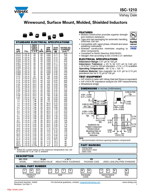
Document Number: 34060For technical questions, contact: magnetics@Revision: 24-Feb-111Wirewound, Surface Mount, Molded, Shielded InductorsISC-1210Vishay DaleNote(1)Rated DC current based on the maximum temperature rise, not to exceed 40 °C at + 85 °C ambientFEATURES•Molded construction provides superior strength and moisture resistance•Tape and reel packaging for automatic handling,2000/reel, EIA-481•Compatible with vapor phase, infrared and wave soldering methodsfio•Shielded construction minimizes coupling to other components•Compliant to RoHS Directive 2002/95/EC•Halogen-free according to IEC 61249-2-21 definitionELECTRICAL SPECIFICATIONSInductance Range: 0.01 μH to 100 μHInductance Tolerance: ± 20 % for 0.01 μH to 0.82 μH;± 10 % for 1.0 μH to 100 μH standard; ± 5 %, ± 3 % available Operating Temperature: - 55 °C to + 125 °CCoilform Material: Non-magnetic for 0.01 μH to 0.10 μH;powdered iron for 0.12 μH to 100 μHTEST EQUIPMENT•H/P 4342A Q meter with Vishay Dale test fixture or equivalent •H/P 4191A RF impedance analyzer (for SRF measurements)•Wheatstone bridge(1)Recommended minimum spacing between componentsSTANDARD ELECTRICAL SPECIFICATIONSIND.(μH)TOL.TEST FREQ.(MHz)Q MIN.SRFMIN.(MHz)DCR MAX.( )RATED DC CURRENT (mA) (1)L & Q 0.010 ± 20 % 505010000.10 8100.012 ± 20 % 505010000.11 7500.015 ± 20 % 505010000.12 7200.018 ± 20 % 505010000.13 6900.022 ± 20 % 504510000.15 6400.027 ± 20 % 504510000.17 6100.033 ± 20 % 504510000.18 5850.039 ± 20 % 504010000.24 5300.047 ± 20 % 504010000.26 4950.056 ± 20 % 504010000.28 4850.068 ± 20 % 504010000.35 4750.082 ± 20 % 50389000.45 4600.10 ± 20 % 50367000.50 4500.12 ± 20 % 25.2405000.20 6300.15 ± 20 % 25.2404700.20 6000.18 ± 20 % 25.2404000.24 5800.22 ± 20 % 25.2403300.30 5650.27 ± 20 % 25.2403100.33 5000.33 ± 20 % 25.2402800.36 4750.39 ± 20 % 25.2402300.40 4650.47 ± 20 % 25.2402200.44 4600.56 ± 20 % 25.2402000.46 4550.68 ± 20 % 25.2401800.48 4500.82 ± 20 % 25.2401600.50 4501.0 ± 10 % 7.96301200.60 4001.2± 10 % 7.96301100.65 3901.5± 10 % 7.963090.0 0.75 3701.8± 10 % 7.963085.0 0.85 3502.2± 10 % 7.963065.0 0.90 3202.7± 10 % 7.963060.0 1.00 2903.3± 10 % 7.963060.0 1.102703.9± 10 % 7.963058.0 1.202504.7± 10 % 7.963052.0 1.252205.6± 10 % 7.963050.0 1.402106.8± 10 % 7.963040.0 1.602058.2± 10 % 7.963035.0 1.6519510.0 ± 10 % 2.523030.0 2.00 18512.0 ± 10 % 2.523024.0 2.3017515.0 ± 10 % 2.523020.0 2.5016518.0 ± 10 % 2.523017.0 2.70.15522.0 ± 10 % 2.523016.0 3.1015027.0 ± 10 % 2.523014.5 3.3012533.0 ± 10 % 2.523014.5 5.1011539.0 ± 10 % 2.523014.0 5.9010547.0 ± 10 % 2.523013.0 8.00 10056.0 ± 10 % 2.523011.510.0 9568.0 ± 10 % 2.523011.0 10.0 9082.0 ± 10 % 2.523011.0 11.0 85100.0 ± 10 % 0.796 306.0 12.0 80PART MARKING- Vishay Dale- Inductance value - Date codeDESCRIPTIONISC-121010 μH± 10 %ERe3MODELINDUCTANCE VALUEINDUCTANCE TOLERANCEPACKAGE CODEJEDEC LEAD (Pb)-FREE STANDARDGLOBAL PART NUMBERIS C121ER100K PRODUCT FAMILYSIZEPACKAGE CODEINDUCTANCEVALUETOL.Legal Disclaimer Notice VishayDisclaimerALL PRODU CT, PRODU CT SPECIFICATIONS AND DATA ARE SU BJECT TO CHANGE WITHOU T NOTICE TO IMPROVE RELIABILITY, FUNCTION OR DESIGN OR OTHERWISE.Vishay Intertechnology, Inc., its affiliates, agents, and employees, and all persons acting on its or their behalf (collectively,“Vishay”), disclaim any and all liability for any errors, inaccuracies or incompleteness contained in any datasheet or in any other disclosure relating to any product.Vishay makes no warranty, representation or guarantee regarding the suitability of the products for any particular purpose or the continuing production of any product. To the maximum extent permitted by applicable law, Vishay disclaims (i) any and all liability arising out of the application or use of any product, (ii) any and all liability, including without limitation special, consequential or incidental damages, and (iii) any and all implied warranties, including warranties of fitness for particular purpose, non-infringement and merchantability.Statements regarding the suitability of products for certain types of applications are based on Vishay’s knowledge of typical requirements that are often placed on Vishay products in generic applications. Such statements are not binding statements about the suitability of products for a particular application. It is the customer’s responsibility to validate that a particular product with the properties described in the product specification is suitable for use in a particular application. Parameters provided in datasheets and/or specifications may vary in different applications and performance may vary over time. All operating parameters, including typical parameters, must be validated for each customer application by the customer’s technical experts. Product specifications do not expand or otherwise modify Vishay’s terms and conditions of purchase, including but not limited to the warranty expressed therein.Except as expressly indicated in writing, Vishay products are not designed for use in medical, life-saving, or life-sustaining applications or for any other application in which the failure of the Vishay product could result in personal injury or death. Customers using or selling Vishay products not expressly indicated for use in such applications do so at their own risk and agree to fully indemnify and hold Vishay and its distributors harmless from and against any and all claims, liabilities, expenses and damages arising or resulting in connection with such use or sale, including attorneys fees, even if such claim alleges that Vishay or its distributor was negligent regarding the design or manufacture of the part. Please contact authorized Vishay personnel to obtain written terms and conditions regarding products designed for such applications.No license, express or implied, by estoppel or otherwise, to any intellectual property rights is granted by this document or by any conduct of Vishay. Product names and markings noted herein may be trademarks of their respective owners.Material Category PolicyVishay Intertechnology, Inc. hereb y certifies that all its products that are identified as RoHS-Compliant fulfill the definitions and restrictions defined under Directive 2011/65/EU of The European Parliament and of the Council of June 8, 2011 on the restriction of the use of certain hazardous substances in electrical and electronic equipment (EEE) - recast, unless otherwise specified as non-compliant.Please note that some Vishay documentation may still make reference to RoHS Directive 2002/95/EC. We confirm that all the products identified as being compliant to Directive 2002/95/EC conform to Directive 2011/65/EU.Revision: 12-Mar-121Document Number: 91000分销商库存信息:VISHAYISC1210ER100K ISC1210ER1R0K ISC1210ER1R2K ISC1210ER1R5K ISC1210ER1R8K ISC1210ER2R2K ISC1210ER2R7K ISC1210ER3R3K ISC1210ER3R9K ISC1210ER4R7K ISC1210ER5R6K ISC1210ER6R8K ISC1210ER8R2K ISC1210SY100K ISC1210SY1R0K ISC1210SY1R2K ISC1210SY1R5K ISC1210SY1R8K ISC1210SY2R2K ISC1210SY2R7K ISC1210SY3R3K ISC1210SY3R9K ISC1210SY4R7K ISC1210SY5R6K ISC1210SY6R8K ISC1210SY8R2K ISC1210ERR15K ISC1210ERR22K ISC1210ERR33K ISC1210ERR39K ISC1210ERR47K ISC1210ERR56K ISC1210ERR82K ISC1210SYR15K ISC1210SYR33K ISC1210SYR39K ISC1210SYR47K ISC1210SYR56K ISC1210SYR82K ISC1210ER10NM ISC1210ER22NM ISC1210ER27NM ISC1210ER33NM ISC1210ER39NM ISC1210ER47NM ISC1210ER56NM ISC1210ER68NM ISC1210ER82NM ISC1210ERR10M ISC1210ERR12M ISC1210ERR15M ISC1210ERR18M ISC1210ERR22M ISC1210ERR27M ISC1210ERR33M ISC1210ERR39M ISC1210ERR47M ISC1210ERR56M ISC1210ERR68M ISC1210ERR82M ISC1210SY10NM ISC1210SY22NM ISC1210SY27NM ISC1210SY33NM ISC1210SY39NM ISC1210SY47NM ISC1210SY56NM ISC1210SY68NM ISC1210SY82NM ISC1210SYR10M ISC1210SYR12M ISC1210SYR15M ISC1210SYR18M ISC1210SYR22M ISC1210SYR27M ISC1210SYR33M ISC1210SYR39M ISC1210SYR47M ISC1210SYR56M ISC1210SYR68M ISC1210SYR82M ISC1210ER15NK ISC1210ER39NK ISC1210ER68NK ISC1210ER82NK ISC1210ERR10K ISC1210SY15NK ISC1210SY39NK ISC1210SY68NK ISC1210SY82NK ISC1210SYR10K ISC1210ER100J ISC1210ER1R0J ISC1210ER1R2J ISC1210ER1R5J ISC1210ER1R8J ISC1210ER2R2J ISC1210ER2R7J ISC1210ER3R3J ISC1210ER3R9J ISC1210ER4R7J ISC1210ER5R6J ISC1210ER6R8J ISC1210ER8R2J ISC1210SY100J ISC1210SY1R0J ISC1210SY1R2J ISC1210SY1R5J ISC1210SY1R8J ISC1210SY2R2J ISC1210SY2R7J ISC1210SY3R3J ISC1210SY3R9J ISC1210SY4R7J ISC1210SY5R6J ISC1210SY6R8J ISC1210SY8R2J ISC1210AN220K ISC1210ER101K ISC1210ER120K ISC1210ER150K ISC1210ER180K ISC1210ER220K。
msc1210芯片资料(中文)

具有 8051 微处理器及闪存的精密模数转换器
一 特性 1 模拟特性 1 24 位无丢失码 2 10Hz 的低噪声下具 22 位有效分辨率 75nV 3 可编程增益放大器 PGA 放大倍数为 1 128 4 片内参考电压的精确度 精度 0.2 漂移 5ppm/ 5 8 个差分/单端通道 6 片内偏置/增益校正 7 偏置漂移 0.02 ppm/ 8 增益漂移 0.5 ppm/ 9 传感器检测 防止芯片烧坏 burn out 10 单周期转换 11 输入缓冲可选 2 数字特性 微处理器内核 1 与 8051 兼容 2 高速内核 每一指令周期占 4 个时钟 3 DC 至 33MHz 4 单条指令执行时间 121ns 5 双重数据指针 内存 1 高达 32KB 的闪速数据内存 FLASH MEMORY 2 分区闪存 3 可经受 1M 次擦除/写操作 数据可保存 100 年 4 系统内部连续编程 串行编程 外部程序/数据存储器 64KB 5 1,280 字节的数据静态存储器 SRAM 6 闪存的内容保护 7 2KB 的引导只读存储器 BOOT ROM 8 可编程的等待状态控制 3 外围特性 1 34 个 I/O 脚 2 附加的 32 位累加器 3 3 个 16 位定时器/计数器 4 系统定时器 5 可编程看门狗定时器 6 2 个完整的双向通用异步收发器 FULL DUPLEX DUAL UART 7 采用直接存储器的主/从串行外围接口 SPI 为 MOTOROLA 公司的一个注册商标 8 16 位 PWM 9 电源管理控制 10 空闲模式下电流<1mA 11 停止模式下电流<1uA
注释
1
若需查询更多电流规格与封装资料
请登陆网站
四 最大额定值 绝对值 1 1 模拟输入 输入电流 输入电流 输入电压 2 供电电源 DVDD 相对于 DGND AVDD 相对于 AGND AGND 相对于 DGND VREF 相对于 AGND
CC1210EX5R110K中文资料
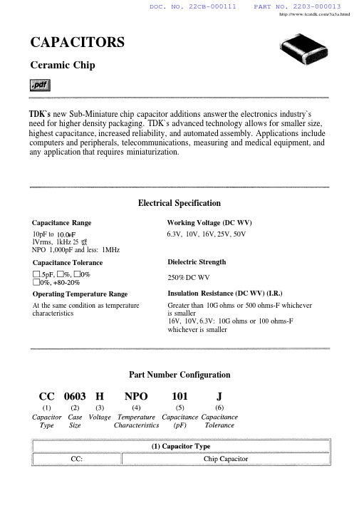
/3a3a.htmlCAPACITORSCeramic ChipTDK`s new Sub-Miniature chip capacitor additions answer the electronics industry`s need for higher density packaging.TDK`s advanced technology allows for smaller size,highest capacitance,increased reliability,and automated assembly.Applications include computers and peripherals,telecommunications,measuring and medical equipment,and any application that requires miniaturization.Capacitance Range10pF tolVrms,1kHz 25NPO 1,000pF and less:1MHzCapacitance Tolerance Operating Temperature RangeAt the same condition as temperaturecharacteristics Working Voltage (DC WV)6.3V,10V,16V,25V,50V Dielectric Strength250%DC WVInsulation Resistance (DC WV)(I.R.)Greater than 10G ohms or 500ohms-F whichever is smaller16V,10V,6.3V:10G ohms or 100ohms-Fwhichever is smallerElectrical SpecificationPart Number ConfigurationDOC. NO. 22CB-000111PART NO. 2203-000013DOC. NO. 22CB-000111PART NO. 2203-000013/3a3a.htmlCeramic Capacitors CAPACITANCE TEMPERATURE CHARACTERISTICS Class IMULTILAYER CERAMIC CHIP CAPACITORSC TYPE [16,25,50Vdc],CLASS I AND CLASS IIClass IICAPACITANCE AND TOLERANCE3-1DOC. NO. 22CB-000111PART NO. 2203-000013Ceramic CapacitorsCAPACITANCE RANGEClass I 25Vdc Class II 16Vdc50Vdc25Vdc50Vdc 3-2Ceramic CapacitorsC TYPE[BASEMETAL ELECTRODE,16,25,50Vdc],CLASS IICAPACITANCE RANGE16Vdc50VdcHC TYPE[LARGECAPACITANCE,16,25,50,75Vdc],CLASS II HIGH DIELECTRIC CONSTANTCAPACITANCE RANGE(Operating temperature range:-25to+85o C[-13 to +185o F])l6Vdc50Vdcc25Vdc 75Vdc3-3Ceramic CapacitorsC TYPE [HIGH VOLTAGE]CLASS I [3kVd c] AND CLASS II [500Vdc,1k,2kVdc]Class I CAPACITANCE TEMPERATURE CHARACTERISTICS CAPACITANCE RANGE Class I 3kVdcClass II500Vdc2kVdclkVdc3-4Ceramic Capacitors FC AND FR TYPE [LOW LOSS FOR VHF/UHF]CLASS I [50,100,200,300,500Vdc]AND CLASS II [50Vdc]Multilayer Ceramic Capacitors for high frequency and low loss are designed for 100to 1000MHz power circuit applications.FC type FR typeCAPACITANCE RANGE (Operating temperature range:-55to +l25o C [-67to +257o F])Class I Class II 50,100,200,300,500Vdc 50VdcCAPACITANCE AND TOLERANCE3-5DOC. NO. 22CB-000111PART NO. 2203-000013。
- 1、下载文档前请自行甄别文档内容的完整性,平台不提供额外的编辑、内容补充、找答案等附加服务。
- 2、"仅部分预览"的文档,不可在线预览部分如存在完整性等问题,可反馈申请退款(可完整预览的文档不适用该条件!)。
- 3、如文档侵犯您的权益,请联系客服反馈,我们会尽快为您处理(人工客服工作时间:9:00-18:30)。
/3a3a.html
CAPACITORS
Ceramic Chip
TDK`s new Sub-Miniature chip capacitor additions answer the electronics industry`s need for higher density packaging.TDK`s advanced technology allows for smaller size,highest capacitance,increased reliability,and automated assembly.Applications include computers and peripherals,telecommunications,measuring and medical equipment,and any application that requires miniaturization.
Capacitance Range
10pF to
lVrms,1kHz 25
NPO 1,000pF and less:1MHz
Capacitance Tolerance Operating Temperature Range
At the same condition as temperature
characteristics Working Voltage (DC WV)6.3V,10V,16V,25V,50V Dielectric Strength
250%DC WV
Insulation Resistance (DC WV)(I.R.)Greater than 10G ohms or 500ohms-F whichever is smaller
16V,10V,6.3V:10G ohms or 100ohms-F
whichever is smaller
Electrical Specification
Part Number Configuration
DOC. NO. 22CB-000111PART NO. 2203-000013
DOC. NO. 22CB-000111PART NO. 2203-000013
/3a3a.html
Ceramic Capacitors CAPACITANCE TEMPERATURE CHARACTERISTICS Class I
MULTILAYER CERAMIC CHIP CAPACITORS
C TYPE [16,25,50Vdc],
CLASS I AND CLASS II
Class II
CAPACITANCE AND TOLERANCE
3-1
DOC. NO. 22CB-000111PART NO. 2203-000013
Ceramic Capacitors
CAPACITANCE RANGE
Class I 25Vdc Class II 16Vdc
50Vdc
25Vdc
50Vdc 3-2
Ceramic Capacitors
C TYPE[BASEMETAL ELECTRODE,16,25,50Vdc],CLASS II
CAPACITANCE RANGE
16Vdc50Vdc
HC TYPE[LARGECAPACITANCE,16,25,50,75Vdc],CLASS II HIGH DIELECTRIC CONSTANT
CAPACITANCE RANGE(Operating temperature range:-25to+85o C[-13 to +185o F])
l6Vdc
50Vdcc
25Vdc 75Vdc
3-3
Ceramic Capacitors
C TYPE [HIGH VOLTAGE]CLASS I [3kVd c] AN
D CLASS II [500Vdc,1k,2kVdc]
Class I CAPACITANCE TEMPERATURE CHARACTERISTICS CAPACITANCE RANGE Class I 3kVdc
Class II
500Vdc
2kVdc
lkVdc
3-4
Ceramic Capacitors FC AND FR TYPE [LOW LOSS FOR VHF/UHF]CLASS I [50,100,200,300,500Vdc]AND CLASS II [50Vdc]Multilayer Ceramic Capacitors for high frequency and low loss are designed for 100to 1000MHz power circuit applications.
FC type FR type
CAPACITANCE RANGE (Operating temperature range:-55to +l25o C [-67to +257o F])Class I Class II 50,100,200,300,500Vdc 50Vdc
CAPACITANCE AND TOLERANCE
3-5DOC. NO. 22CB-000111PART NO. 2203-000013。
