FS8054线性锂离子电池充电芯片
锂电池管理芯片分类

锂电池管理芯片分类
锂电池管理芯片主要可以分为以下几类:
1.线性锂电池芯片,例如SL1053。
这款芯片是专门为高精度的线性锂电池充电器而设计的,非常适合低成本、便携式的充电器使用。
它集成了高精度的预充电、恒定电流充电、恒定电压充电、电池状态检测、温度监控、充电结束低泄漏、充电状态指示等功能,可以广泛应用于PDA、移动电话、手持设备等领域。
2.恒定电流/恒定电压线性充电器,例如TP4056和CH4054。
这些芯片可为单节锂离子电池提供恒定的电流和恒定的电压进行线性充电。
其中,CH4054还具有热反馈功能,能够自动调节充电电流以限制芯片温度在大功率操作或高环境温度条件下的增长。
3.开关模式充电器,例如HL7016。
这是国内首款12V高压输入全集成的开关模式充电器,实现了高输入电压和USBOTG升压模式及I2C接口可编程。
4.智能型电池充电管理芯片,例如CS0301和CN3052A。
这些芯片具有功能全、价格低、集成度高,外部电路简单,调节方便等特点。
瑞通电子线性单元Li-Ion电池充电IC说明书
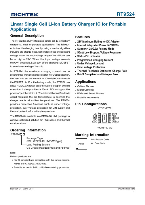
DS9524-01 April 2011Ordering InformationNote :Richtek products are :` RoHS compliant and compatible with the current require-ments of IPC/JEDEC J-STD-020.` Suitable for use in SnPb or Pb-free soldering processes.Pin ConfigurationsWDFN-10L 3x2(TOP VIEW)Linear Single Cell Li-Ion Battery Charger IC for Portable ApplicationsGeneral DescriptionThe RT9524 is a fully integrated single cell Li-ion battery charger IC ideal for portable applications. The RT9524optimizes the charging task by using a control algorithm including pre-charge mode, fast charge mode and constant voltage mode. the input voltage range of the VIN pin can be as high as 28V. When the input voltage exceeds the OVP threshold, it will turn off the charging MOSFET to avoid overheating of the chip.In RT9524, the maximum charging current can be programmed with an external resistor. For USB application,the user can set the current to 100mA/500mA through the EN/SET pin. For the factory mode, the RT9524 can allow 4.2V/2.3A power pass through to support system operation. It also provides a 50mA LDO to support the power of peripheral circuit. The internal thermal feedback circuit regulates the die temperature to optimize the charge rate for all ambient temperatures. The RT9524provides protection functions such as under voltage protection, over voltage protection for VIN supply and thermal protection for battery temperature.The RT9524 is available in a WDFN-10L 3x2 package to achieve optimized solution for PCB space and thermal considerations.Featuresz 28V Maximum Rating for DC Adapter z Internal Integrated Power MOSFETs z Support 4.2V/2.3A Factory Modez 50mA Low Dropout Voltage Regulator z Status Pin Indicatorz Programmed Charging Current z Under Voltage Lockout z Over Voltage Protectionz Thermal Feedback Optimized Charge Rate zRoHS Compliant and Halogen FreeApplicationsz Cellular Phones z Digital Camerasz PDAs and Smart Phones zProtable InstrumentsMarking InformationA0 : Product CodeW : Date CodeISET IEOCGND PGB CHGSB GND EN/SETLDOVIN BATT G : Green (Halogen Free and Pb Free)Typical Application CircuitFunction Block DiagramDS9524-01 April 2011Electrical CharacteristicsTo be continuedRecommended Operating Conditions (Note 3)z Supply Input Voltage, V IN ----------------------------------------------------------------------------------------------4.3V to 5.5V z Junction T emperature Range ------------------------------------------------------------------------------------------−40°C to 125°C zAmbient T emperature Range ------------------------------------------------------------------------------------------ −20°C to 85°CAbsolute Maximum Ratings (Note 1)z Supply Input Voltage, V IN ----------------------------------------------------------------------------------------------−0.3V to 28V z Other Pins -----------------------------------------------------------------------------------------------------------------−0.3V to 6V zPower Dissipation, P D @ T A = 25°CWDFN-10L 3x2----------------------------------------------------------------------------------------------------------- 1.111W zPackage Thermal Resistance (Note 2)WDFN-10L 3x2, θJA ------------------------------------------------------------------------------------------------------90°C/W WDFN-10L 3x2, θJC -----------------------------------------------------------------------------------------------------15°C/W z Lead Temperature (Soldering, 10 sec.)-----------------------------------------------------------------------------260°C z Junction T emperature ---------------------------------------------------------------------------------------------------150°CzStorage Temperature Range -------------------------------------------------------------------------------------------−65°C to 150°C(V IN= 5V, V BATT = 4V, T A = 25°C, unless otherwise specified)Note 1. Stresses listed as the above“Absolute Maximum Ratings”may cause permanent damage to the device. These are for stress ratings. Functional operation of the device at these or any other conditions beyond those indicated in the operational sections of the specifications is not implied. Exposure to absolute maximum rating conditions for extended periods may remain possibility to affect device reliability.Note 2. θJA is measured in the natural convection at T A = 25°C on a high effective thermal conductivity four-layer test board of JEDEC 51-7 thermal measurement standard. The measurement case position of θJC is on the exposed pad of the package.Note 3. The device is not guaranteed to function outside its operating conditions.DS9524-01 April 2011VOUT Regulation Voltage vs. Input Voltage4.1954.2004.2054.2104.2154.2204.2254.54.945.385.826.266.7Input Voltage (V)V O U T R e g u l a t i o n V o l t a g e (V)VOUT Sleep Leakage Current vs. Battery Voltage0481216201.31.72.12.52.93.33.74.14.5Battery Voltage (V)V O U T S l e e p L e a k a g e C u r r e n t (µA )Input OVP Threshold vs. Temperature6.706.726.746.766.786.806.826.84-50-25255075100125Temperature (°C)I n p u t O V P T h r e s h o l d (V )Typical Operating CharacteristicsLDO Voltage vs. Temperature4.854.874.894.914.934.95-50-25255075100125Temperature (°C)L D O V o l t a g e (V)LDO Output Voltage vs. Output Current4.854.874.894.914.934.9520406080100Output Current (mA)L D O O u t p u t V o l t a g e (V)VOUT Regulation Voltage vs. Temperature4.1854.1904.1954.2004.2054.2104.215-50-25255075100125Temperature (°C)V O U T R e g u l a t i o n V o l t a g e (V )EN/SET Shut-DownTime (1ms/Div)V IN = 5VEN/SEB (1V/Div)VLDO (2V/Div)I CHARGER (500mA/Div)CHGS (2V/Div)Power On Time (10ms/Div)PGB (2V/Div)V IN (5V/Div)V BATT = 3.8V, R ISET = 680Ω, EN/SEB = LowCHGSB (2V/Div)I CHARGER (500mA/Div)USB 100 Mode Charge Current vs. Input Voltage8590951004.54.95.35.76.16.5Input Voltage (V)Ch a r g e C u r r e n t (m A )ISET Voltage vs. Input Voltage1.471.481.491.501.511.521.534.24.725.245.766.286.8Input Voltage (V)I S E T V o l t a g e (V )USB 500 Mode Charge Current vs. Input Voltage3653753853954054154.54.95.35.76.16.5Input Voltage (V)Ch a r g e C u r r e n t (m A )ISET Mode Charge Current vs. Input Voltage3003754505256006757508259004.54.95.35.76.16.5Input Voltage(V)C h a r ge C u r r e n t (m A )DS9524-01 April 2011Factory ModeTime (50μs/Div)V IN = 5V , C OUT = 44μF, I OUT = 10Ω to 2.3ΩVIN (5V/Div)VBA TT (200mV/Div)EN/SET (1V/Div)I OUT (1A/Div)LDO Load Transient ResponseTime (250μs/Div)V IN = 5V, V BATT = 3.8V, I LDO = 5mA to 50mAVLDO _ac(100mV/Div)I LDO(500mA/Div)Time (1ms/Div)V IN = 5V, V BATT = 3.8V, R ISET = 680ΩVIN (5V/Div)VBA TT (5V/Div)EN/SET (2V/Div)I CHARGER (500mA/Div)VIN (5V/Div)VBA TT(5V/Div)EN/SET (2V/Div)I CHARGER (500mA/Div)V IN = 5V, V BATT = 3.8V, R ISET = 80ΩTime (1ms/Div)Application InformationDescriptionThe RT9524 is a fully integrated low cost single-cell Li-Ion battery charger IC with a constant current mode (CC mode) or a constant voltage mode (CV mode). The charge current is programmable to USB100, USB500 or ISET mode and the CV mode voltage is fixed at 4.2V. The pre-charge threshold is fixed at 2.5V. If the battery voltage is below the pre-charge threshold, the RT9524 charges the battery with a trickle current until the battery voltage rises above the pre-charge threshold. The RT9524 is capable of being powered up from AC adapter and USB (Universal Serial Bus) port inputs. Moreover, the RT9524 include a linear regulator (LDO 4.9V, 50mA) for supplying low power external circuitry.ACIN Over Voltage ProtectionThe input voltage is monitored by the internal comparator and the input over voltage protection threshold is set to 6.9V. However, input voltage over 28V will still cause damage to the RT9524. When the input voltage exceeds the threshold, the comparator outputs a logic signal to turn off the power P-MOSFET to prevent the high input voltage from damaging the electronics in the handheld system. When the input over voltage condition is removed, the comparator re-enables the output by running through the soft-start.Charger Enable and mode SettingEN/SET is used to enable or disable the charger as well as to select the charge current limit. Drive the EN pin to low or leave it floating to enable the charger. The EN/SET pin has a 200kΩ internal pull down resistor. So, when left floating, the input is equivalent to logic low. Drive this pin to high to disable the charger. After the EN/SET pin pulls low for 50μs, the RT9524 enters the USB500 mode and wait for the setting current signal. EN/SET can be used to program the charge current during this cycle. The RT9524 will change its charge current by sending different pulse to EN/SET pin. If no signal is sent to EN/SET, the RT9524 will remain in USB500 mode. A correct period of time for high pulse is between 100μs and 700μs and the period of pulse to pulse must be between 100μs and 700μs to be properly read. Once EN/SET is held low for 1.5ms,the number of pulses is locked and sent to the control logic and then the mode changes. The RT9524 needs to be restarted to reset the charge current. Once the EN/ SET input is held high for more than 1.5ms, the RT9524 is disabled.Table 1. Pulse Counting Map for EN/SET InterfaceFigure .1 (b)Battery Charge ProfileThe RT9524 charges a Li-Ion battery with a constant current (CC) or a constant voltage (CV).The constant current is decided by the operation mode of USB100, USB500 or ISET mode. The constant current is set with the external resistor R ISET and the constant voltage is fixed at 4.2V. If the battery voltage is below the Pre-Charge Threshold, the RT9524 charges the battery with a trickle current until the battery voltage rises above the trickle charge threshold. When the battery voltage reaches 4.2V, the charger enters CV mode and regulates the battery voltage at 4.2V to fully charge the battery without the risk of over chargingFigure .1 (a)IIDS9524-01 April 2011Battery Pre-Charge CurrentDuring a charge cycle, if the battery voltage is below the pre-charge threshold, the RT9524 enters the pre-charge mode. This feature revives deeply discharged cells and protects battery. Under USB100 Mode, the pre-charge current is internally set to 95mA. When the RT9524 is under USB500 and ISET Mode, the pre-charge current is 20% of fast-charge current set by external resistor R ISET .Battery Fast-Charge Current ISET ModeThe RT9524 offers ISET pin to program the charge current.The resistor R ISET is connected to ISET and GND. The parameter K ISET is specified in the specification table.ISEF Charge ISEF ISETKI = ; K = 530R USB500 and USB100 ModeThe fast-charge current is 95mA in USB100 mode and 395mA in USB500 mode. Note that if the fast-charge current set by external resistor is smaller than that in USB500 mode (395mA), the RT9524 charges the battery in ISET mode.Battery Voltage Regulation (CV Mode)The battery voltage regulation feedback is through the BATT pin. The RT9524 monitors the battery voltage between BATT and GND pins. When the battery voltage closes in on the battery regulation voltage threshold, the voltage regulation phase begins and the charging current begins to taper down. When the charging current falls below the programmed end-of-charge current threshold,the CHGSB pin goes high to indicate the termination of charge cycle.The end-of-charge current threshold is set by the IEOC pin. The resistor R EOC is connected to IEOC and GND.The parameters K EOC and IEOC are specified in the specification table.EOC EOC EOC EOC RI (%) = ; K = 200K The current threshold of IEOC (%) is defined as the percentage of fast-charge current set by R ISET . After the CHGSB pin is pulled high, the RT9524 still monitors the battery voltage. Charge current is resumed when the battery voltage goes to lower than the battery regulation voltage threshold.Factory ModeThe RT9524 provides factory mode for supplies up to 2.3A for powering external loads with no battery installed and BATT is regulated to 4.2V. The factory mode allows the user to supply system power with no battery connected.In factory mode, thermal regulation is disabled but thermal protection (155°C) is still active. When using currents greater than 1.5A in factory mode, the user must limit the duty cycle at the maximum current to 20% with a maximum period of 10ms.LDOThe RT9524 integrates one low dropout linear regulator(LDO) that supplies up to 50mA. The LDO is active whenever the input voltage is between POR threshold andFigure 2Figure 32004006008001000120014000.40.60.81 1.2 1.4 1.61.82 2.22.4 2.62.83R SET ∠)B a t t e r yC h a r g e C u r r e n t (m A )(k ΩOVP threshold. It is not affected by the EN/SET input.Note that the LDO current is independence and not monitored by the charge current limit.Charge Status Outputs (CHGSB and PGB)The open-drain CHGSB and PGB outputs indicate various charger operations as shown in the following table. These status pins can be used to drive LEDs or communicate to the host processor. Note that ON indicates the open-drain transistor is turned on and LED is bright.Table 2Sleep ModeThe RT9524 enters sleep mode if the power is removed from the input. This feature prevents draining the battery during the absence of input supply.Temperature Regulation and Thermal Protection In order to maximize charge rate, the RT9524 features a junction temperature regulation loop. If the power dissipation of the IC results in a junction temperature greater than the thermal regulation threshold (125°C), the RT9524 limits the charge current in order to maintain a junction temperature around the thermal regulation threshold (125°C). The RT9524 monitors the junctiontemperature, T J , of the die and disconnects the battery from the input if T J exceeds 125°C. This operation continues until junction temperature falls below thermal regulation threshold (125°C) by the hysteresis level. This feature prevents maximum power dissipation from exceeding typical design conditions.Selecting the Input and Output CapacitorsIn most applications, all that is needed is a high-frequency decoupling capacitor on the input. A 1μF ceramic capacitor,placed in close proximity to input to GND, works well. Insome applications depending on the power supplycharacteristics and cable length, it may be necessary toadd an additional 10μF ceramic capacitor to the input.The RT9524 requires a small output capacitor for loop stability. A typical 1μF ceramic capacitor placed between the BATT pin and GND is sufficient.Thermal ConsiderationsFor continuous operation, do not exceed absolutemaximum operation junction temperature. The maximum power dissipation depends on thermal resistance of the IC package, PCB layout, rate of surrounding airflow, and difference between junction and ambient temperature. Themaximum power dissipation can be calculated by thefollowing formula :P D(MAX) = (T J(MAX) − T A ) / θJAwhere T J(MAX) is the maximum operation junctiontemperature, T A is the ambient temperature, and θJA is thejunction to ambient thermal resistance.For recommended operating conditions specification of RT9524, the maximum junction temperature is 125°C and T A is the maximum ambient temperature. The junction to ambient thermal resistance, θJA , is layout dependent. For WDFN-10L 3x2 packages, the thermal resistance, θJA , is 90°C/W on a standard JEDEC 51-7 four-layer thermal test board. The maximum power dissipation at T A = 25°C can be calculated by the following formula :P D(MAX) = (125°C − 25°C) / (90°C/W) = 1.111W for WDFN-10L 3x2 packageThe maximum power dissipation depends on operating ambient temperature for fixed T J(MAX) and thermal resistance, θJA . For RT9524 package, the derating curveRT952411DS9524-01 April 2011in Figure 4 allows the designer to see the effect of rising ambient temperature on the maximum power dissipation.Figure 4. Derating Curve for RT9524 Package Layout ConsiderationThe RT9524 is a fully integrated low cost single-cell Li-Ion battery charger IC ideal for portable applications. Careful PCB layout is necessary. For best performance, place all peripheral components as close to the IC as possible. A short connection is highly recommended. The following guidelines should be strictly followed when designing a PCB layout for the RT9524.`Input capacitor should be placed close to the IC and connected to ground plane. The trace of input in the PCB should be placed far away from the sensitive devices or shielded by the ground.`The GND should be connected to a strong ground plane for heat sinking and noise protection.`The connection of R ISET and R IEOC should be isolated from other noisy traces. The short wire is recommended to prevent EMI and noise coupling.`Output capacitor should be placed close to the IC and connected to ground plane to reduce noise coupling.Figure 5. PCB Layout GuideThe capacitor should be placed close to IC pin and The connection of resistor should be isolated from other noisy traces. Short to prevent EMI and noise coupling.ground plane for heat sinking and noise protection.0.00.20.40.60.81.01.2255075100125Ambient Temperature (°C)M a x i m u m P o w e r D i s s i p a t i o n (W )12DS9524-01 April 2011Richtek Technology CorporationHeadquarter5F, No. 20, Taiyuen Street, Chupei City Hsinchu, Taiwan, R.O.C.Tel: (8863)5526789 Fax: (8863)5526611Richtek Technology CorporationTaipei Office (Marketing)5F, No. 95, Minchiuan Road, Hsintien City Taipei County, Taiwan, R.O.C.Tel: (8862)86672399 Fax: (8862)86672377Email:*********************Information that is provided by Richtek Technology Corporation is believed to be accurate and reliable. Richtek reserves the right to make any change in circuit design, specification or other related things if necessary without notice at any time. No third party intellectual property infringement of the applications should be guaranteed by users when integrating Richtek products into any application. No legal responsibility for any said applications is assumed by Richtek.W-Type 10L DFN 3x2 Package。
锂电池充电控制芯片

锂电池充电控制芯片CHK0501特点概述●具备涓流、恒流、恒压三段式充电方式CHK0501是一款具备涓流,恒流,恒压三段式充电方式的锂电池充电控制芯片,并具有电池短路、过温保护功能。
●●具有电池短路、过温保护功能具有温度端检测和电流检测两种判断电池有无的方式芯片内置了高精度和高电源抑制能力的基准电压源,从而实现了极高精度的浮充电压控制,充分保证了充电的安全性。
内置电源稳压电路,简化了外围电路。
输出控制端(DRC)耐压高达40V,可以实现多节电池充电控制。
●●●●●单端口驱动双色LED内置低端采样电路输出控制端耐压高达40V内置电源稳压电路,±2%精度内置高精度基准电路(-40℃~+85℃,基准电压为1.2V±5mV)SOP8封装芯片具有完善的锂电池充电保护功能,极大地提高了电池的充电寿命(次数)和电池的充电安全性。
●芯片采用SOP8封装。
管脚排列图1CHK0501系列管脚排列V BAT Rs=150mΩ,I=300mA● 1.188 1.200 1.212电池I CONST Rs=150mΩRs=150mΩRs=150mΩ●0.9331 1.067AI PRE●●6767-1001000.84.70.3-133133-mAmAVI FULLV DRCDRC驱动能力LED高电平驱动能力LED低电平驱动能力LED闪烁频率极限参数芯片可承受最大功率-------800mW工作温度---------40℃~+85℃结温---------------------150℃输入端口电压----0.3~VDD+0.3V 储存温度-------40℃~+125℃焊接温度(锡焊,10秒)--300℃注:超出所列的极限参数可能导致器件的永久性损坏。
以上给出的仅仅是极限范围,在这样的极限条件下工作,器件的技术指标将得不到保证,长期在这种条件下还会影响器件的可靠性。
电学参数(●代表全工作温度范围,没有这个符号表示测试温度为25℃,除非另外指定)符号VDD Idd参数测试条件最小4.9-典型5最大5.1-单位V 电源电压稳压值芯片工作电流浮充门槛电压恒流充电电流涓流充电电流判饱电流Idd=1mA,LED悬空●VDD=5.0V,LED悬空0.5mAVVDD=5V,I=50mADRCV LEDH LEDL VDD=5V,I LEDH=-5mA--VV VDD=5V,I LEDL=5mA--VF LED VDD=5V●●0.31HzLV 端各门槛V LH涓流转恒流门槛VDD=5V,V电池由低到高0.57450.6500.6355V VLHYS涓流转恒流门槛迟滞短路判断电●mV V LL CHK0501C/D VDD=5V●0.520.550.58-V 压VNULL无电池判断电压VDD=5VVDD=5VVDD=5VVDD=5V----4.50.350.6VVVVVT端各门槛V OT过温电压回温电压--V RTV IJ转换为电流判断模式电压0.05-注:与LV、VT相关的各个参考电压值,实际上是由VDD分压而来的,4.5V对应0.9*VDD,0.6V对应0.12*VDD,以此类推。
锂电池充电管理芯片__概述说明以及概述

锂电池充电管理芯片概述说明以及概述1. 引言1.1 概述锂电池充电管理芯片是一种关键性的电子元件,广泛应用于各种设备和系统中,用于控制和管理锂电池的充电过程。
随着现代科技的不断进步和锂电池在移动设备、可穿戴设备、电动汽车以及能源存储系统等领域的广泛应用,对高效安全的充电管理方案的需求也越来越迫切。
本文将对锂电池充电管理芯片进行全面概述,并介绍其定义、原理、功能特点以及应用领域。
此外,还将详细解释充电管理芯片的工作原理,包括充电控制功能、温度监测和保护机制以及电压和电流检测技术。
在实际应用案例分析部分,我们将通过手机电池充电管理芯片实践案例、电动汽车充电管理芯片实践案例以及太阳能储能系统中的充电管理芯片实践案例来展示该技术在不同领域中的应用情况。
最后,在结论与展望部分将总结文章中主要观点和要点,并对未来发展趋势提出展望和建议。
通过深度理解锂电池充电管理芯片的特点和工作原理,有助于推动相关技术的创新发展,提升锂电池充电效率和安全性。
本文旨在为读者提供关于锂电池充电管理芯片的全面介绍,并激发对该领域研究的兴趣,促进更广泛的应用和进一步发展。
2. 锂电池充电管理芯片2.1 定义和原理:锂电池充电管理芯片是一种集成电路,它主要用于监测和控制锂电池的充电过程。
它通过与锂电池进行连接,并采集关键参数,如温度、电压和电流等。
然后,根据这些数据,利用内部算法实现对充电过程的精确控制。
锂电池充电管理芯片的工作原理基于以下几个关键方面:首先,它能够对输入的直流信号进行转换和处理,以获得所需的信息。
例如,可以通过采样来测量锂电池的电压和充放电过程中的实时电流。
其次,芯片具备自我保护机制,能够在有异常情况出现时及时断开充电回路,从而防止因过热、过压或其他故障导致锂电池发生损坏或事故。
此外,在不同情况下(如温度变化、大功率输入等)还可以根据芯片内部预设的算法调整充电策略和参数设置。
2.2 功能和特点:锂电池充电管理芯片具备以下主要功能:1) 充电控制功能:芯片可根据充放电状态实时调整充电方式和策略,确保锂电池的安全和高效充电。
高精度线性内置MOS管双节锂电池充电器控制电路
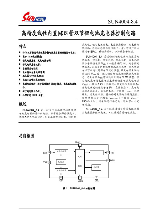
特点8.4V 双节锂离子或锂聚合物电池充电器的理想控制电路;高于1%的电压精度;恒定电流充电,充电电流可调; 恒定电压充电过程; 自动再充电过程;双LED 充电状态指示; 电池不正常状态的检测;电源电压低时,处于低功耗的Sleep 模式,电池漏电流极小;极少的外围元器件;小型化的SOP8封装;概述SUN4004_8.4是一款专门为高精度的线性锂电池充电器而设计的电路,非常适合那些低成本、便携式的充电器使用。
它集高精度预充电、恒定电流充电、恒定电压充电、电池状态检测、充电结束低泄漏、充电状态指示等性能于一身,可以广泛地使用于EPC 、移动多媒体、手持设备等领域。
SUN4004_8.4通过检测电池电压来决定其充电状态:预充电、恒流充电、恒压充电。
当电池电压小于阈值电压V MIN (一般为6V )时,处于预充电状态,以较小的电流对电池进行充电,预充电的电流可以通过外部电阻进行调整。
预充电使电池电压达到V MIN 后,进入恒定电流充电的快速充电状态,充电电流I REG 可以通过外围电阻R1调整,恒定电流充电使电池电压上升到恒定电压充电电压V REG (一般为8.4V )。
然后进入恒定电压充电状态,充电电压的精度优于±1%,在该状态下,充电电流将逐渐减小,当充电电流小于阈值I TERM ,充电结束。
充电结束后,将始终对电池电压进行监控,当电池电压小于阈值V RECHG (一般为V REG -250mV )时,对电池进行再充电,进入下一个充电周期。
功能框图LEDSDRNGNDBAT CS1RG高精度线性内置MOS管双节锂电池充电器控制电路电池饱和结束电压可调;SUN4004_8.4还可以通过调节外围电阻来提高电池饱和结束电压,可以设到需要的电压点。
无锡日晟微电子有限公司SUN4004-8.4订购信息管脚排列引脚描述LEDS VCC DRN BAT LEDT CS1RG引脚名称 引脚序号 I/O引脚功能LEDS 1 O充电状态指示。
多节锂电池充电管理芯片

多节锂电池充电管理芯片多节锂电池充电管理芯片(Multi-Cell Lithium Battery Charging Management Chip)随着电子设备的普及和移动应用的广泛应用,对电池的需求也愈发增加。
多节锂电池的设计因其高容量和高能量密度而被广泛应用于电动汽车、电动工具、无人机等领域。
多节锂电池的充电管理是提高电池性能和延长使用寿命的关键。
因此,多节锂电池充电管理芯片的研发和应用具有重要意义。
多节锂电池充电管理芯片是一种用于控制和管理电池充电过程的集成电路。
它通常由电路管理单元(Management Unit),放电保护单元(Discharge Protection Unit),充电控制单元(Charging Control Unit)和通信接口单元(Communication Interface Unit)等组件构成。
充电芯片的主要功能是实现对电池的合理充电和放电控制,同时保护电池免受过充、过放、过流和过温等问题的影响。
它还能够通过通信接口与外部设备进行数据交互,实现对电池充电和放电过程的监测和控制。
多节锂电池充电管理芯片的工作原理是通过对电池电压、电流和温度等参数的监测和控制,实现对电池充电和放电过程的控制和管理。
当电池电压低于一定阈值时,充电控制单元会启动充电,将电压升至设定的充电终止电压。
当电池电压超过一定阈值时,放电保护单元会切断电池的充电电源,防止过充。
同时,多节锂电池充电管理芯片还具备过放保护、过流保护和过温保护等功能,以保护电池免受异常工作条件的影响。
多节锂电池充电管理芯片具有许多优点。
首先,它能够实现对电池的智能化充电和放电管理,提高电池的性能和稳定性。
其次,多节锂电池充电管理芯片体积小、功耗低,便于集成到各种电子设备中。
最后,多节锂电池充电管理芯片具有良好的可靠性和安全性,可以有效延长电池的使用寿命,减少电池故障的发生。
然而,目前市面上多节锂电池充电管理芯片的种类繁多,功能各异。
充电ADS8054(2YL6)
3.4 170 1.25 1.2 100 30 0.1 0.1 1.03 20 0.35
100 120
100 2 1000 1
单位
V mV V V mV mV mA mA V µA V
mV °C
µs ms µs µA
PROG脚电压 CHRG 脚弱下拉电流 CHRG 脚输出低电压 二次电池隔值电压 恒温条件下结温 软启动时间 二次充电比较器的滤波器滞后时间 终止充电比较器的滤波器滞后时间 PROG脚上拉电流
电源从低到高时
PROG脚电压上升时 PROG 脚电压下降时 电源从低到高时 电源从高到低时 RPROG = 10K(4) RPROG = 2K RPROG = 10K, 充电 VCHRG = 5V ICHRG = 5mA VFLOAT - VRECHRG
标注 1: 超过绝对极限值可能会损坏 IC。
标注 2:超出它的工作范围 IC 不能保证正常工作。 标注 3: 支持电流包括 PROG 脚电流(近似100µA),但不包括通过BAT脚流到电池的电流 (近似
100mA). 标注 4: ITERM 是 PROG 脚电阻设定充电电流值的一部分。
ADS INT' L GROUP CO. ,LIMITED
ADS 8054
独立线性锂电充电器 ADS8054
概述
ADS8054是 一 款 完 整 的 单 节 锂 离 子 电 池 恒 流 恒 压 线 性 充 电 IC 。 它 采 用 极 小 的 SOT-23-5 封 装 , 只 需 要 外 接 极 少 的 外 部 元 件 ,使 它 能 真 正 的 适 用 于 便 携 式 产 品 的 应 用 。 而 且 ,A D S 8 0 5 4 是 专 门 为 U S B 电 源 特 性 而 设 计 的 。同 时 ,A D S 8 0 5 4 也 能 作 为 一 个 独 立 的 线 性锂离子电池充电器。
锂电池充电管理IC

联益微LY4056带反接保护锂电池充电IC阳先生13 5300 03 912联益微LY4054恒流涓流锂电池充电ICQ: 98 61267 86联益微LY3085锂电池4.35V充电IC两种封装SOT23-5/SOP8联益微LY4056锂电池4.35V充电IC两种封装SOT23-5/SOP8联益微LY3085锂电池4.35V充电IC两种封装SOT23-5/SOP8联益微LY4057反接保护锂电池充电IC联益微LY5057双节锂电池充电芯片IC联益微Ly6600双节2A开关充电IC联益微LY6057线性1A锂电池充电IC联益微LY9899联益微5V/1A内置MOS高效率升压IC联益微LY8355联益微5V/1A外置MOS高效率升压IC联益微LY6291联益微5V/1A低成本高效率升压IC联益微LY3400联益微5V/500MA低成本高效率升压IC联益微LY1039联益微5V/1A移动电源方案联益微LY1026联益微5V/2A移动电源方案联益微LY9833联益微5V/3A移动电源方案联益微LY1035联益微2.8V 内置肖特基升压IC联益微LY1035联益微3.0V内置二极管升压IC联益微LY1040联益微2.5V无感升压IC联益微LY4060联益微5V无感升压IC联益微LY1029联益微外置MOS做2.1A升压IC供应LY7135联益微LED手电筒恒流驱动IC供应联益微LY6206物美价廉稳压IC稳压ICLY6291联益微3,7v升压5v 1a大电流的移动方案LY1035联益微2.7V/2.8V/3.0V升压IC鼠标专用LY7136联益微LED手电筒1W恒流驱动ICLY2326联益微LED手电筒3W恒流驱动ICLY1029联益微ipod移动电源方案LY2106联益微升压恒流1-3w手电筒ICLY4430联益微半导体强势供应1-15W手电筒方案。
TP4057 600mA 锂电池充电器 V2.1 产品说明书

概述TP4057 是一款单节锂离子电池恒流/恒压线性充电器,简单的外部应用电路非常适合便携式设备应用,适合 USB 电源和适配器电源工作,内部采用防倒充电路,不需要外部隔离二极管。
热反馈可对充电电流进行自动调节,以便在大功率操作或高环境温度条件下对芯片温度加以限制。
TP4057充电截止电压为 4.2V ,充电电流可通过外部电阻进行设置。
当充电电流降至设定值的 1/10 时,TP4057 将自动结束充电过程。
当输入电压被移掉后,TP4057 自动进入低电流待机状态,将待机电流降至 3uA 。
特点∙ 最大充电电流:600mA∙ 无需MOSFET 、检测电阻器和隔离二极管 ∙ 智能热调节功能可实现充电速率最大化 ∙ 智能再充电功能 ∙ 预充电压:4.2V±1% ∙ C/10充电终止 ∙ 2.9V 涓流充电阈值∙ 单独的充电、结束指示灯控制信号 ∙封装形式:SOT23-6L应用∙ 手机、PDA 、MP3/MP4 ∙ 蓝牙耳机、GPS ∙充电座∙数码相机、Mini 音响等便携式设备典型应用电路管脚SOT23-6L 定购信息极限参数(注1)注1电气参数(注2,3)注3:规格书的最小、最大规范范围由测试保证,典型值由设计、测试或统计分析保证。
内部框图工作原理TP4057是专门为一节锂离子电池或锂聚合物电池而设计的线性充电器,芯片集成功率晶体管,充电电流可以用外部电阻设定,最大持续充电电流可达1A,不需要另加阻流二极管和电流检测电阻。
TP4057包含两个漏极开路输出的状态指示端,充电状态指示输出端CHRG和充电完成指示输出端STDBY 。
充电时管脚CHRG输出低电平,表示充电正在进行。
如果电池电压低于2.9V,TP4057用小电流对电池进行预充电。
当电池电压超过2.9V时,采用恒流模式对电池充电,充电电流由PROG管脚和GND之间的电阻R PROG确定。
当电池电压接近4.2V电压时,充电电流逐渐减小,TP4057进入恒压充电模式。
单节锂电池充电管理芯片,IC电路图全集

产品特点1,可达500MA 充电电流,SOT23-5,单LED 指示灯,5V 输入线性降压,PW40542,可达1000MA 充电电流,SOP8-EP ,双LED 指示灯,5V 输入线性降压,PW40563,可达600MA 充电电流,SOT23-5,单LED 指示灯,5V 输入线性降压,输入输出短路保护4,可达2.50A 充电电流,SOP8-EP ,双LED 指示灯,5V 输入开关降压,PW40525,可达3.0A 充电电流,SOP8-EP ,双LED 指示灯,5V 输入开关降压,PW40356,可达2.0A 充电电流,SOP8-EP ,单LED 指示灯,5-20V 输入开关降压,PW42037,LDO 稳压芯片(2V-80V ),DC-DC 降压芯片,DC-DC 升压芯片选型表PW4054是一款性能优异的单节锂离子电池恒流/恒压线性充电器。
PW4054适合给USB 电源以及适配器电源供电。
基于特殊的内部MOSFET 架构以及防倒充电路,PW4054不需要外接检测电阻和隔离二极管。
当外部环境温度过高或者在大功率应用时,热反馈可以调节充电电流以降低芯片温度。
充电电压固定在 4.2V ,而充电电流则可以通过一个电阻器进行外部设置。
当充电电流在达到M A X 终浮充电压之后降至设定值的1/10,芯片将终止充电循环。
当输入电压断开时,PW4054进入睡眠状态,电池漏电流将降到1uA 以下。
PW4054还可以被设置于停机模式,此时芯片静态电流降至25uA 。
PW4054还包括其他特性:欠压锁定,自动再充电和充电状态标志⚫可编程充电电流500mA ⚫无需外接MOSFET ,检测电阻以及隔离二极管⚫恒定电流/恒定电压并具有可在无过热危险的情况下实现充电速率M A X 大化的热调节功能。
⚫精度达到±1%的4.2V 预充电电压⚫用于电池电量检测的充电电流监控器输出⚫自动再充电⚫充电状态输出显示⚫C/10充电终止⚫待机模式下的静态电流为25uA ⚫ 2.9V 涓流充电⚫软启动限制浪涌电流PW4065 是一款完整的单节锂电池充电器,带电池正负极反接保护、 输入电源正负极反接保 护的芯片,兼容大小 3mA-600mA 充电电流。
锂电池充电管理芯片CN3052A

高性能的线性锂电池充电管理芯片CN3052A/CN3052B/CN3056的应用CN3052A/CN3052B/CN3056是高性能的线性锂电池充电管理芯片。
这些器件内部集成有功率管,不需要外部的电流检测电阻和阻流二极管,只需要极少的外围元器件,并且符合USB总线技术规范,可以通过USB端口为锂电池充电,因此非常适用于各种充电器及MP4播放器、蓝牙耳机、数码相机等便携式产品。
图1是一个典型的应用电路图。
图1:CN3052A/CN3052B/CN3056的典型应用电路图CN3052A/CN3052B/CN3056的工作流程图2是CN3052A/CN3052B/CN3056的充电过程示意图。
当输入电压大于电源低电压检测阈值和芯片使能输入端接高电平时,CN3052A/CN3052B/CN3056开始对电池充电,CHRG管脚输出低电平,表示充电正在进行。
如果电池电压低于3V,充电器用小电流对电池进行预充电。
当电池电压超过3V时,充电器采用恒流模式对电池充电,充电电流由ISET管脚和GND之间的电阻RISET<确定。
当电池电压接近电池端调制电压4.2V时,充电电流逐渐减小,CN3052A/CN3052B/CN3056进入恒压充电模式。
图2:CN3052A/CN3052B/CN3056充电过程示意图当充电电流减小到充电结束阈值时,CHRG端输出高阻态,表示充电周期结束,充电结束阈值是恒流充电电流的10%。
如果要开始新的充电周期,只要将输入电压断电,然后再上电就可以了,或者将CE管脚的电压暂时拉到0V,再恢复到高电平。
当电池电压降到再充电阈值以下时,自动开始新的充电周期。
当输入电压低于电池电压时,充电器进入低功耗的睡眠模式,电池端消耗的电流小于3uA,从而增加了待机时间。
如果将使能输入端CE接低电平,充电器被关断。
CN3052A/CN3052B/CN3056的主要功能介绍电源低电压检测(UVLO) CN3052A/CN3052B/CN3056内部有电源电压检测电路,当电源电压低于电源电压过低阈值(典型值4.03V)时,芯片处于关断状态,充电也被禁止。
SI4054B(0.5A线性锂离子电池充电器 IC)
IBAT = 0 to 1000V/RPROG
IPROG
PROG上拉电流
注:1、超出最大工作范围可能会损坏芯片。 2、芯片不建议工作在极限参数的状态下。
第3页共5页
150
mV
120
℃
100
us
1000
us
1
uA
SI4054B
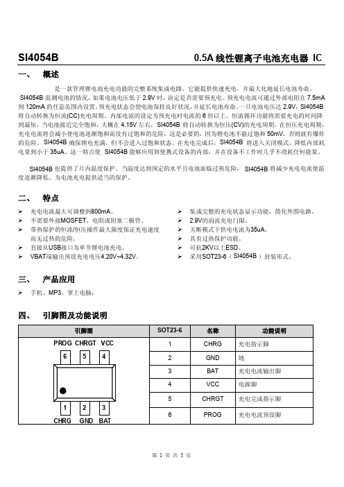
0.5A 线性锂离子电池充电器 IC
3、芯片的工作电流包括PROG Pin外面电阻消耗的电流(约100uA),但不包括芯片通过BAT Pin给芯片充电的 电流(约100mA)。
Rprog
GND
第4页共5页
SI4054B
九、 封装尺寸图
SOT23-6
0.5A 线性锂离子电池充电器 IC
第5页共5页
654
123 CHRG GND BAT
SOT23-6 1 2 3 4 5 6
名称 CHRG GND BAT VCC CHRGT PROG
功能说明 充电指示脚 地 充电电流输出脚 电源脚 充电完成指示脚 充电电流预设脚
第1页共5页
1
2
SI4054B
五、 应用电路图
0.5A 线性锂离子电池充电器 IC
A
符号 VCC VIN VPROG VBAT VCHRG
θJA IBAT IPROG TJ TJ TS
额定值 7
-0.3 to 7 VCC+0.3
7 7 Continuous 连续 75 (DIP/SOP8) 800 800 125 -40 to 85 -65 to 125 300
单位 V V V V V
RPROG = 2k, Current Mode
500
mA
TC4054(0.5A线性锂离子电池充电器 IC)中文技术资料
TC4054(文件编号:S&CIC1076)0.5A线性锂离子电池充电器IC一、概述TC4054是恒流/恒压座充充电器芯片,主要应用于单节锂电池充电。
无需外接检测电阻,其内部为MOSFET 结构,因此无需外接反向二极管。
TC4054在大功率和高环境温度下可以调节充电电流以限制芯片温度。
它的充电电压固定在4.2V,充电电流可以通过外置一个电阻器进行调节。
当达到浮充电压并且充电电流下降到设定电路的1/10时,TC4054自动终止充电过程。
当输入电压移开之后,TC4054自动进入低电流模式,从电池吸取少于2uA的电流。
当TC4054进入待机模式时,供电电流小于25uA。
TC4054还可以监控充电电流,具有电压检测、自动循环充电的特性,并且具有一个指示管脚指示充电终止状态和输入电压状态。
二、特性可达500mA的可编程充电电流无需外接MOSFET、检测电阻、反向二极管恒流/恒压模式操作,具有热保护功能可通过USB端口为锂电池充电具有1%精度的预设充电电压待机模式下电流为20uA2.9V涓流充电电压软启动限制了浪涌电流采用SOT23-5封装TC4054(文件编号:S&CIC1076)0.5A线性锂离子电池充电器ICTC4054(文件编号:S&CIC1076)0.5A线性锂离子电池充电器IC 七、电气特性(V=5V;T J=25℃,除非另有说明)IN注:1、超出最大工作范围可能会损坏芯片。
2、超出器件工作参数极限,不保证其正常功能。
3、电源电流包括PROG端电流(大约100uA),不包括通过BAT端传输到电池的其他电流(大约100uA)。
4、充电终止电流一般是设定充电电流的0.1倍。
TC4054(文件编号:S&CIC1076)0.5A线性锂离子电池充电器IC八、波形图浮动电压VS电源电压充电电流VS 电源电压涓流充电电流VS电源电压浮动电压VS 温度TC4054(文件编号:S&CIC1076)0.5A线性锂离子电池充电器IC九、封装尺寸图SOT23-5。
单节锂电充电路径管理芯片
单节锂电充电路径管理芯片单节锂电充电路径管理芯片是一种用于单节锂电池的充电管理的集成电路,具有充电保护、充电均衡、电池状态监测等功能。
本文将详细介绍单节锂电充电路径管理芯片的工作原理、主要特点以及在电子产品中的应用。
一、工作原理单节锂电充电路径管理芯片根据锂电池的特性,采用不同的电路设计实现充电管理功能。
主要包括以下几个部分:1. 充电保护:当锂电池电压过高或过低时,芯片会自动切断充电电流,以避免锂电池过充或过放引起的安全问题。
2. 充电均衡:由于锂电池的内阻和容量存在差异,充电均衡功能可以实现对每个电池单体进行均衡充电,提高整个电池组的使用寿命和性能。
3. 电池状态监测:芯片可以监测电池的电压、电流和温度等参数,以实时了解电池的工作状态,从而保护电池安全和延长电池寿命。
二、主要特点单节锂电充电路径管理芯片具有以下几个主要特点:1. 高集成度:通过集成充电保护、均衡和监测功能于一体,实现了高度集成化的设计,减小了电路板的体积和复杂度。
2. 低功耗:芯片采用低功耗设计,能够实现高效的充电管理,提高电池的使用时间和续航能力。
3. 安全可靠:芯片具有多重保护功能,能够及时监测和处理电池异常情况,以保障用户的安全使用。
4. 灵活性强:充电路径管理芯片可以根据不同的锂电池特性进行定制化设计,满足不同产品的需求。
三、应用领域单节锂电充电路径管理芯片广泛应用于各类电子产品中,如移动智能设备、无线传感器、电动工具等。
以下是几个常见的应用场景:1. 移动智能设备:如智能手机、平板电脑等移动设备,需要使用单节锂电池进行供电,单节锂电充电路径管理芯片可以确保电池安全充电,延长电池寿命。
2. 电动工具:如电动扳手、电动螺丝刀等电动工具常使用单节锂电池供电,芯片可以实现对电池的充电保护,提高电池的使用寿命和性能。
3. 无线传感器:无线传感器需要使用电池供电,单节锂电充电路径管理芯片可以监测电池状态,确保稳定的供电,提高传感器的工作效率和可靠性。
QX4054锂电池恒流恒压线性充电控制器
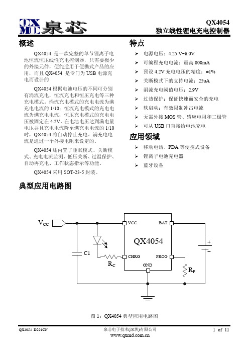
典型应用电路图V CC图1:QX4054典型应用电路图概述 QX4054 是一款完整的单节锂离子电池恒流恒压线性充电控制器,只需要极少的外接元件,便能适用于便携式产品的应用,而且QX4054 是专门为USB 电源充电而设计的 QX4054根据电池电压的不同可分别有涓流充电,恒流充电和恒压充电等三种充电模式。
涓流充电模式的充电电流为满充电电流的1/10;恒流充电模式的充电电流为满充电电流;恒压充电模式的充电电压被固定在4.2V ,在电池电压达到满电量电压并且充电电流降至满充电电流的1/10时,QX4054将自动停止充电。
满充电电流是通过一个外接电阻来设定的。
QX4054还内置了睡眠模式、关断模式、充电电流监测、低压关断、过温保护、自动再充电、工作状态指示等功能。
QX4054采用SOT-23-5封装。
特点 电源电压:4.25 V~6.0V 可编程充电电流:最高800mA 预设4.2V 充电电压的精度:±1% 关断模式下的支持电流:25uA涓流充电阈值电压:2.9V过热保护:保证快速而安全的充电 软启动:有效限制冲击电流无需外接MOS 管、感应电阻和二极管 可从USB 口直接给电池充电 应用领域移动电话、PDA 等便携式设备 锂离子电池充电器 蓝牙设备订货信息产品型号QX4054封装及管脚分配PROG VCC54132GNDCHRG BATSOT-23-5管脚定义内部电路方框图VCC CHRGBAT PROG图2:QX4054的内部电路方框图极限参数(注1)注1:超过上表中规定的极限参数会导致器件永久性损坏,而工作在以上极限条件下可能会影响器件的可靠性。
电特性除非特别说明,V CC =5V ,T A =25o C电特性(接上一页)除非特别说明,V CC=5V,T A =25o C电特性(接上一页)除非特别说明,V CC=5V,T A =25ºC注2:支持电流包括PROG 脚电流(近似100µA),但不包括通过BA T脚流到电池的电流(近似100mA). 注3:I TER M是PROG脚电阻设定充电电流值的一部分。
大功率降压恒流芯片给电池充电

大功率降压恒流芯片给电池充电嘿,大家好,今天咱们聊聊一个很酷的东西,那就是大功率降压恒流芯片给电池充电。
听起来复杂?别担心,咱们用最简单的语言来解读这个神奇的小玩意儿。
你有没有发现,电池就像是你的好朋友,总是在关键时刻给你送来能量。
手机没电了,哎呀,这可怎么办?没有电,就像没了心肝宝贝,生活顿时暗淡无光。
但是,如果用上了大功率降压恒流芯片,情况就大不一样了。
这个小家伙就像是电池的“营养师”,确保它能吸收恰到好处的电量,不多不少,刚刚好。
简直是电池充电界的福音。
想象一下,你在户外露营,突然发现手机没电了。
天哪,那真是大煞风景,无法拍照、无法导航,感觉就像是迷了路的羊。
此时,如果你有一个搭载了降压恒流芯片的充电宝,嘿,马上就可以解决问题。
这个芯片就像是个聪明的调皮鬼,知道怎么控制电流,不让电池“吃撑”也不让它“饿肚子”。
这样一来,电池的寿命就能长长久久,跟老寿星似的,一直陪着你。
这个芯片还有一个好处,就是它的效率特别高。
说白了,能量转换几乎没有浪费。
想想你家里的电器,有时候开着开着就热得像蒸笼一样,那是浪费电。
可这个芯片可不一样,工作时就像个高效的“勤快人”,省电又省心。
你充一次电,就能用很久很久,简直是划算得不行。
对了,还有个细节,大家都知道,电池充电的时候,有时候会出现发热现象。
哎,心疼!可是大功率降压恒流芯片能有效控制温度,避免电池过热,就像给电池穿上了“防护衣”,让它安全又舒适。
咱们也不能忽视这个芯片的使用场景。
比如在电动车上,这可是个重头戏。
电动车充电,别的芯片可能会把电流一下子泼上去,结果电池就像个喝醉酒的小伙伴,受不了啊。
而用上降压恒流芯片,电流就温柔得多,慢慢来,电池才能保持最佳状态。
这样不但延长了电池的使用寿命,还能让你开车更放心,毕竟谁都不想在路上“没电”。
说到这里,可能有人会问,这个芯片的成本是不是很高?现代科技的发展让这个芯片变得越来越普及,价格也亲民得多。
就好比买个新手机,不用非得跟顶级款拼,选择一个适合的,既好用又省钱,何乐而不为呢?未来,随着技术不断进步,降压恒流芯片的应用会越来越广泛,从家庭小电器到工业设备,处处都能见到它的身影。
pn8054工作原理
pn8054工作原理pn8054是一种工作原理先进的芯片,它在电子设备中起着重要的作用。
本文将介绍pn8054的工作原理及其在电子设备中的应用。
我们来了解一下pn8054的工作原理。
pn8054是一种集成电路芯片,它采用了先进的半导体技术。
该芯片内部包含了多个电子元件,如晶体管、电容器和电阻器等。
这些元件通过精确的布局和连接,形成了一个复杂的电路结构。
在工作时,pn8054通过外部电源提供电能,并根据输入信号的变化来控制内部电路的工作状态。
具体来说,当输入信号发生变化时,pn8054会根据设定的逻辑电路规则,将输入信号转换为相应的输出信号。
这个转换过程是通过电子元件之间的互动实现的。
例如,当输入信号为高电平时,pn8054会使相应的晶体管导通,从而使相应的输出信号为高电平;当输入信号为低电平时,pn8054会使相应的晶体管截止,从而使相应的输出信号为低电平。
pn8054的工作原理可以理解为一个信息处理的过程。
它接收来自外部的输入信号,经过内部的逻辑运算和信号转换,最终得到输出信号。
这种信号转换的过程是非常快速和精确的,因此pn8054在电子设备中得到了广泛的应用。
接下来,我们来看一下pn8054在电子设备中的应用。
由于pn8054具有高度集成的特点,它可以用于各种电子设备中,如手机、电脑、电视等。
在手机中,pn8054可以用于控制屏幕的亮度和色彩,实现更加清晰和逼真的显示效果。
在电脑中,pn8054可以用于控制硬盘的读写速度,提高电脑的运行效率。
在电视中,pn8054可以用于控制声音的输出和图像的处理,提供更好的视听体验。
除了上述应用外,pn8054还可以用于各种传感器和测量设备中。
例如,它可以用于温度传感器,通过测量温度变化并将其转换为电信号,实现对温度的监测和控制。
另外,pn8054还可以用于压力传感器、湿度传感器等,实现对环境参数的测量和监测。
pn8054是一种工作原理先进的芯片,它通过精确的电路设计和信号转换,实现了电子设备的控制和处理功能。
- 1、下载文档前请自行甄别文档内容的完整性,平台不提供额外的编辑、内容补充、找答案等附加服务。
- 2、"仅部分预览"的文档,不可在线预览部分如存在完整性等问题,可反馈申请退款(可完整预览的文档不适用该条件!)。
- 3、如文档侵犯您的权益,请联系客服反馈,我们会尽快为您处理(人工客服工作时间:9:00-18:30)。
5480FS DATASHEETShenZhen Fanhai Microelectronics Co.,LtdThe FS8054 converters are available in the The FS8054 automatically terminates the rmore, the FS8054 is specifically designed t xternal component count make the FS8054 i The FS8054 is a complete constant-current/F e a t u r e sProgrammable Charge Current Up to800mANo MOSFET, Sense Resistor or BlockingDiode RequiredComplete Linear Charger for Single CellLithium-Ion BatteriesConstant-Current/Constant-VoltageOperation with Thermal Regulation* to Maximize Charge RateWithout Risk of Overheating Charges Single Cell Li-Ion BatteriesDirectly from USB PortPreset 4.2V Charge Voltage with 1%AccuracyAutomatic Recharge65uA Supply Current in Shutdown 2.9V Trickle Charge Threshold Available in 5-Lead SOT-23 PackageA p p l i c a t i o n sCharger for Li-Ion Coin Cell Batteries Portable MP3 Players, Wireless Headsets Bluetooth Applications Multifunction Wristwatches D e s c r i p t i o nconstant voltage linear charger for single cell lithium-ion batteries. Its package and low e deally suited for portable applications. Furthe o work within USB power specifications. No external sense resistor is needed, and no blocking diode is required due to the internal MOSFET architecture. Thermal feedback regulates the charge current to limit the die temperature during high power operation or high ambient temperature. The charge voltage is fixed at 4.2V, and the charge current can be programmed externally with a single resistor. charge cycle when the charge current drops to 1/10th the programmed value after the final float voltage is reached.industry standard SOT-23-5 power packages (or upon request).O r d e r I n f o r m a t i o n① ②:SYMBOLDESCRIPTION① Denotes Output voltage: 4.2V②Denotes Package Types: E: SOT-23-5T y p i c a l A p p l i c a t i o nUH8**P i n A s s i g n m e n tAbsolute Maximum RatingsInput Supply Voltage (VCC) ..................................................................... ................... –0.3V to 7V PROG.................................................................................................. ........... – 0.3V to VCC + 0.3V BAT ......................................................................................................................... –0.3V to 7V CHRG..................................................................................................................... –0.3V to 7V BAT Short-Circuit Duration .............................................................................................. Continuous BAT Pin Current ..................................................................................................................... 800mA Maximum Junction Temperature .............................................................................................. 125℃ Operating Ambient Temperature Range................................................................ –40℃ to 85℃ Storage Temperature Range …………………………………………….................. –65 ℃to 125℃ Lead Temperature (Soldering, 10 sec)..................................................................................... 300℃PIN NUMBER SOT-23- 5PIN NAMEFUNCTION1 CHRG Open-Drain Charge Status Output2 GND Ground3 BAT Charge Current Output 4V CCPositive Input Supply Voltage.5PROGCharge Current Program,Charge Current Monitor and Shutdown PinUN8**E l e c t r i c a l C h a r a c t e r i s t i c sOperating Conditions: T A =25, ℃V CC =5V unless otherwise specified.SYMBOLPARAMETERCONDITIONSMINTYPMAXUNITSV CC Input Supply Voltage4.55.06.5 VI CCInput Supply CurrentCharge Mode , R PROG = 10k Standby Mode (Charge Terminated) lShutdown Mode (R PROG Not Connected, V CC < V BAT , or V CC < VUV)70 45 65µA µA µAV FLOATRegulated Output (Float) Voltage0℃≤T A ≤85℃, I BAT = 50mA 4.15 4.2 4.24 V I BAT BAT Pin CurrentR PROG = 10k, Current Mode R PROG = 2k, Current Mode Standby Mode, V BAT = 4.2V Shutdown Mode (R PROG Not Connected)Sleep Mode, V CC = 0V83 41089 445 7.3 7.2 0.397 470 15 1 mA mAµA µA µA I TRIKL Trickle Charge Current V BAT < V TRIKL , R PROG = 2k 15 39 65 mA V ASD V CC – V BAT Lockout Threshold Voltage V CC from Low to High V CC from High to Low5 18mV I TERM C/10 Termination Current Threshold R PROG = 2k45 mA V PROG PROG Pin Voltage R PROG = 10k, Current Mode 0.94 1.02 1.08 V R ONEfficiencyPower FET “ON” Resistance (Between VCC and BAT)660m Ωof the BAT pin voltage, the SD8054 enters shutdown m A p p l i c a t i o n I n f o r m a t i o nPIN ASSIGNMENTCHRG (Pin 1): Open-Drain Charge Status Output. When the battery is charging, the CHRG pin ispulled low by an internal N-channel MOSFET. When the charge cycle is completed or reverse battery lockout / No AC is detected, CHRG is forced high impedance.GND (Pin 2): Ground.BAT (Pin 3): Charge Current Output. It should be bypassed with at least a 1uF capacitor. It Providescharge current to the battery and regulates the final float voltage to 4.2V. An internal precision resistor divider from this pin sets the float voltage which is disconnected in shutdown mode.V CC (Pin 4): Positive Input Supply Voltage. It Provides power to the charger VCC can range from4.30V to 6.5V and should be bypassed with at least a 1uF capacitor. When VCC drops to within 20mV ode, dropping IBAT to less than 1 uA.PROG (Pin 5): Charge Current Program, Charge Current Monitor and Shutdown Pin. The chargecurrent is programmed by connecting a 1% resistor, RPROG, to ground. When charging in constant-current mode, this pin servos to 1V. In all modes, the voltage on this pin can be used to measure the charge current using the following formula: IBAT = (VPROG/RPROG)*890, The PROG pin can also be used to shut down the charger. Disconnecting the program resistor from ground allows a weak current to pull the PROG pin high. When it reaches the 1.21V shutdown threshold voltage, the charger enters shutdown mode, charging stops and the input supply current drops to 65uA. Reconnecting RPROG to ground will return the charger to .normal operation.P a c k a g i n g I n f o r m a t i o nSOT-23-5 Package Outline DimensionDimensions In MillimetersDimensions In Inches Symbol Min Max Min Max A 1.050 1.250 0.041 0.049 A1 0.000 0.100 0.000 0.004 A2 1.050 1.150 0.041 0.045 b 0.300 0.500 0.012 0.020 c 0.100 0.200 0.004 0.008 D 2.820 3.020 0.111 0.119 E 1.500 1.700 0.059 0.067 E1 2.6502.9500.1040.116e 0.950(BSC) 0.037(BSC) e1 1.800 2.000 0.071 0.079 L0.3000.600 0.0120.024。