MC1374中文资料
MC34167MC33167中文资料
MC34167 MC331671简介该MC34167, MC33167系列单片电源开关可用于dc–to–dc优化调节器申请.这些器件的固定频率,电压模式稳压器包含了所有的积极作用需要直接和实施step–down以最小的转换数量voltage–inverting外部元件.它们也可以用于成本效益在step–up转换器应用.潜在市场包括汽车,计算机,工业和成本敏感的消费产品.每一个设备的部分介绍给下面与代表框图所示图13.2振荡器振荡器频率内部编程72 kHz的电容CT和修剪电流源.该充放电率控制在产生一个95%在开关输出的最大占空比.在CT的放电,振荡器产生内部消隐脉冲持有的反相输入与门高,禁用输出开关晶体管.标称振荡器峰值和山谷门槛4.1 V和2.3 V分别.3脉宽调制器脉宽调制器由一个比较器振荡器斜坡电压施加到非反相输入端,而误差放大器的输出应用到反相输入.输出开关导通时启动CT检查排放到振荡器峰谷电压.至于收费的CT电压超过误差放大器的输出,锁存复位,终止输出晶体管的导通时间振荡器的ramp–up时期.这PWM /锁存结合防止在给定的多输出脉冲振荡器时钟周期.数字6和14说明开关输出电压与占空比的补偿.4电流检测该系列采用MC34167当前cycle–by–cycle限制,作为保护手段输出开关晶体管从过度紧张.在每个周期视为一个单独的情况.电流限制是通过监测输出开关晶体管的电流传导期间建设,并经检测过流情况,请立即关闭为振荡器的ramp–up期内开关.集电极电流转换为电压由内部微调电阻和对一个参考比较由电流检测比较器.当电流限制达到阈值,比较器重置PWM 锁存.限流门限点往往设在6.5 A.图9说明开关与输出电流限制门槛温度.5误差放大器和参考一个误差放大器的高增益提供了访问反相输入和输出.该放大器具有典型dc电压增益80 dB,和单位增益带宽600 kHz与相边缘 70度(图3).同相输入偏置内部5.05 V参考并且不固定了.参考具有精度±2.0%在室温下.以提供负载5.0 V中,参考编程50以上mV 5.0 V补偿在电缆的电压降和1.0%从连接器转换器输出.如果转换器设计需要一个输出电压高于5.05 V,电阻更大R1必须加入形成一个分压网络的反馈输入中所示数字13和18.了确定输出方程与分压网络的电压为:Vout+5.05R2R1)1外部回路补偿所需的转换器稳定.一个简单的low–pass滤波器是由连接电阻(R2)从稳压输出到反相输入,以及一系列resistor–capacitor (RF, CF)之间Pins 1和5.补偿网络的元件值显示在电路的申请被选定为each在稳定工作条件下进行测试.该step–down转换器(图18)是最容易补偿稳定.该step–up(图20)和voltage–inverting(图22)配置运作,连续导反激式转换器,而且更难以弥补.该最简单的方法来优化网络是补偿观察输出电压的负载响应一步变化,而调整临界阻尼RF和CF.该最终电路应验证以下四个稳定边界条件.这些条件是最小和最大输入电压,最小和最大负载.通过箝位的电压误差放大器的输出(引脚5)不到150 mV,内部电路将放置到一个低功耗待机模式,从而将权力电源电流36µA与12 V电源电压.图10说明了备用电源电流与电源电压.误差放大器的输出有一个100µA电流源pull–up,可用于实现soft–start.图17显示充电电流源通过一个电容CSS系列二极管.该二极管断开从反馈CSS回路电阻时1.0 M操作它上面的收费销5.范围开关输出输出开关晶体管的设计最大的40 V,以最小的峰值集电极电流时5.5 A.配置为step–down或voltage–inverting应用,如在图18和22,电感会把偏置的输出整流开关关闭时.整流器与较高的正向电压降或长期拖延的时间应该打开不能使用.如果发射器被允许去充分负,集电极电流流过,造成额外的装置暖气,降低转换效率.图8显示到箝位的发射器0.5集电极电流V,在一系列的100µA温度过高.阿1N5825或肖特基势垒整流器相当于推荐履行这些要求.欠压分离欠压分离一直比较成立以保证完全集成电路在输出级的功能已启用.内部参考电压比较器的监测使输出阶段VCC超过5.9 V.为了防止不稳定的输出交叉切换的阈值,0.9 V迟滞.6摩托罗拉设备数据模拟ICMC34167 MC33167热保护内部热关断电路,以保护在事件集成电路的最大结温度超过.当被激活时,通常在170°C,是被迫的锁存成'复位'的状态,关闭输出开关.此功能防止灾难性故障提供偶然的设备过热.它的目的不是要作为一个适当的散热片的替代品.该MC34167包含在5–lead TO–220类型包装.该标签包装是很常见的中心引脚(引脚3),通常连接到地.设计考虑不要试图建立一个转换器上wire–wrap或plug–in原型板.特别应注意分开的信号电流和接地接地通路从负载电流路径.所有高电流回路应尽可能短尽可能使用重型铜runs到尽量减少振荡和辐射EMI.为了获得最佳的操作,严密元件布局建议.电容器Cin, CO,和所有的反馈元件应尽可能靠近IC在身体可能.这也是必须的肖特基二极管连接到开关输出是尽可能靠近尽可能IC.图15.低功耗待机电路+100µA错误放大器1图16.过电压关断电路+100µA错误放大器1120补偿5120补偿R15R1I =待机模式VShutdown = VZener + 0.7图17. Soft–Start电路+100µA错误放大器1120补偿D2Vin1.0 MCss5D1R1tSoft–Start≈35,000 Css。
34712资料
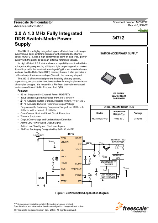
Document number: MC34712Rev. 4.0, 5/2007Freescale Semiconductor Advance Information* This document contains certain information on a new product.Specifications and information herein are subject to change without notice.© Freescale Semiconductor, Inc., 2007. All rights reserved.3.0 A 1.0 MHz Fully Integrated DDR Switch-Mode Power SupplyThe 34712 is a highly integrated, space efficient, low cost, single synchronous buck switching regulator with integrated N-channel power MOSFETs. It is a high performance point-of-load (PoL) power supply with the ability to track an external reference voltage.Its high efficient 3.0 A sink and source capability combined with its voltage tracking/sequencing ability and tight output regulation, makes it ideal to provide the termination voltage (V TT ) for modern data buses such as Double-Data-Rate (DDR) memory buses. It also provides a buffered output reference voltage (V REF ) to the memory chipset The 34712 offers the designer the flexibility of many control,supervisory, and protection functions to allow for easy implementation of complex designs. It is housed in a Pb-Free, thermally enhanced, and space efficient 24-Pin Exposed Pad QFN.Features•45 m Ω Integrated N-Channel Power MOSFETs •Input Voltage Operating Range from 3.0 V to 6.0 V•±1 % Accurate Output Voltage, Ranging from 0.7 V to 1.35 V •±1 % Accurate Buffered Reference Output Voltage•Programmable Switching Frequency Range from 200 kHz to 1.0 MHz with a default of 1.0 MHz•Over Current Limit and Short Circuit Protection •Thermal Shutdown•Output Overvoltage and Undervoltage Detection •Active Low Power Good Output Signal •Active Low Standby and Shutdown Inputs•Pb-Free Packaging Designated by Suffix Code EP.Figure 1. 34712 Simplified Application DiagramSWITCH-MODE POWER SUPPLYEP SUFFIX 98ARL10577D 24-PIN QFN34712ORDERING INFORMATIONDevice Temperature Range (T A )Package MC34712EP/R2-40 to 85°C24 QFNV INMCUPVINVREFINVIN VDDI FREQ GND SDSTBYBOOTSWVOUT INV COMP VREFOUTPGND PGDDR MEMORY CONTROLER34712V DDQDDR MEMORY CHIPSET V INV REFV TTV DDQV DDQMEMORY BUSTERMINATING RESISTORS(3.0V TO 6.0V)INTERNAL BLOCK DIAGRAMINTERNAL BLOCK DIAGRAMFigure 2. 34712 Simplified Internal Block Diagram34712Analog Integrated Circuit Device DataAnalog Integrated Circuit Device Data 34712PIN CONNECTIONSPIN CONNECTIONSFigure 3. 34712 Pin ConnectionsTable 1. 34712 Pin DefinitionsA functional description of each pin can be found in the Functional Pin Description section beginning onpage 10.Pin NumberPin Name Pin Function Formal Name Definition1GND Ground Signal GroundAnalog signal ground of IC2FREQ Passive Frequency Adjustment Buck converter switching frequency adjustment pin3NC None No Connect No internal connections to this pin4PG Output Power Good Active-low (open drain) power-good status reporting pin 5STBY Input Standby Standby mode input control pin 6SDInput Shutdown Shutdown mode input control pin 7VREFIN Input Voltage-Tracking-Reference Input Voltage-Tracking-Reference voltage input8VREFOUTOutput Reference VoltageOutput Buffered output equal to 1/2 of voltage-tracking reference 9COMPPassive Compensation Buck converter external compensation network pin 10INV Input Error Amplifier Inverting Input Buck converter error amplifier inverting input pin11VOUT Output Output Voltage Discharge FET Discharge FET drain connection (connect to buck converter output capacitors)12,13,14PGND Ground Power Ground Ground return for buck converter and discharge FET 15,16,17SW Power Switching Node Buck converter power switching node 18,19,20PVIN Supply Power-Circuit SupplyInputBuck converter main supply voltage input21BOOTPassiveBootstrapBootstrap switching node (connect to bootstrap capacitor)GND FREQ STBY PG NC SDV R E F I NC O M PI N VV O U TP G N DSW P V I NB O O TV I NV D D IV R E F O U TPGND PGNDSW SWPVIN P V I NV I NAnalog Integrated Circuit Device Data34712PIN CONNECTIONS22,23VINSupply Logic-Circuit SupplyInput Logic circuits supply voltage input24VDDIPassiveInternal Voltage RegulatorInternal Vdd Regulator (connect filter capacitor to this pin)Table 1. 34712 Pin Definitions (continued)A functional description of each pin can be found in the Functional Pin Description section beginning on page 10.Pin NumberPin NamePin FunctionFormal Name DefinitionAnalog Integrated Circuit Device Data 34712ELECTRICAL CHARACTERISTICSMAXIMUM RATINGSELECTRICAL CHARACTERISTICSMAXIMUM RATINGSTable 2. Maximum RatingsAll voltages are with respect to ground unless otherwise noted. Exceeding these ratings may cause a malfunction or permanent damage to the device.RatingsSymbolValueUnitELECTRICAL RATINGS Input Supply Voltage (VIN) PinV IN -0.3 to 7.0V High-Side MOSFET Drain Voltage (PVIN) Pin PV IN -0.3 to 7.0V Switching Node (SW) PinV SW -0.3 to 7.5V BOOT Pin (Referenced to SW Pin)V BOOT - V SW-0.3 to 7.5V PG, VOUT, SD, and STBY Pins--0.3 to 7.0V VDDI, FREQ, INV, COMP, VREFIN, and VREFOUT Pins --0.3 to 3.0V Continuous Output Current (1)I OUT±3.0AESD Voltage (2)Human Body Model Device Charge Model (CDM)V ESD1V ESD3±2000±750VTHERMAL RATINGSOperating Ambient Temperature (3)T A -40 to 85°C Storage TemperatureT STG -65 to +150°C Peak Package Reflow Temperature During Reflow (4), (5)T PPRT Note 5°C Maximum Junction Temperature T J(MAX)+150°C Power Dissipation (T A = 85 °C) (6)P D2.9WNotes1.Continuous output current capability so long as T J is ≤ T J(MAX).2.ESD1 testing is performed in accordance with the Human Body Model (C ZAP = 100 pF, R ZAP = 1500 Ω), ESD3 testing is performed inaccordance with the Charge Device Model (CDM).3.The limiting factor is junction temperature, taking into account power dissipation, thermal resistance, and heatsinking.4.Pin soldering temperature limit is for 10 seconds maximum duration. Not designed for immersion soldering. Exceeding these limits maycause malfunction or permanent damage to the device.5.Freescale’s Package Reflow capability meets Pb-free requirements for JEDEC standard J-STD-020C. For Peak Package ReflowTemperature and Moisture Sensitivity Levels (MSL),Go to , search by part number [e.g. remove prefixes/suffixes and enter the core ID to view all orderable parts. (i.e. MC33xxxD enter 33xxx), and review parametrics.6.Maximum power dissipation at indicated ambient temperature.Analog Integrated Circuit Device Data34712ELECTRICAL CHARACTERISTICS MAXIMUM RATINGSTHERMAL RESISTANCE (7)Thermal Resistance, Junction to Ambient, Single-Layer Board (1s) (8)R θJA 139°C/W Thermal Resistance, Junction to Ambient, Four-Layer Board (2s2p) (9)R θJMA 43°C/W Thermal Resistance, Junction to Board (10)R θJB22°C/WNotes7.The PVIN, SW, and GND pins comprise the main heat conduction paths.8.Per SEMI G38-87 and JEDEC JESD51-2 with the single-layer board (JESD51-3) horizontal.9.Per JEDEC JESD51-6 with the board (JESD51-7) horizontal. There are no thermal vias connecting the package to the two planes in theboard.10.Thermal resistance between the device and the printed circuit board per JEDEC JESD51-8. Board temperature is measured on the topsurface of the board near the package.Table 2. Maximum Ratings (continued)All voltages are with respect to ground unless otherwise noted. Exceeding these ratings may cause a malfunction or permanent damage to the device.RatingsSymbolValueUnitAnalog Integrated Circuit Device Data 34712ELECTRICAL CHARACTERISTICSSTATIC ELECTRICAL CHARACTERISTICSSTATIC ELECTRICAL CHARACTERISTICSTable 3. Static Electrical CharacteristicsCharacteristics noted under conditions 3.0 V ≤ V IN ≤ 6.0 V, - 40°C ≤ T A ≤ 85°C, GND = 0 V unless otherwise noted. Typical values noted reflect the approximate parameter means at T A = 25°C under nominal conditions unless otherwise noted.CharacteristicSymbolMinTypMaxUnitIC INPUT SUPPLY VOLTAGE (VIN) Input Supply Voltage Operating Range V IN 3.0- 6.0VInput DC Supply Current (11)Normal Mode: SD = 1 & STBY = 1, Unloaded Outputs I IN --25mAInput DC Supply Current (11)Standby Mode, SD = 1 & STBY = 0I INQ --15mAInput DC Supply Current (11)Shutdown Mode, SD = 0 & STBY = XI INOFF--100µAINTERNAL SUPPLY VOLTAGE OUTPUT (VDDI)Internal Supply Voltage RangeV DDI2.352.52.65VBUCK CONVERTER (PVIN, SW, GND, BOOT, INV, COMP)High-side MOSFET Drain Voltage Range P VIN 2.5- 6.0V Output Voltage Adjustment Range (12)V OUT 0.7- 1.35V Output Voltage Accuracy (12), (13), (14)--1.0- 1.0%Line Regulation (12)Normal Operation, V IN = 3.0 V to 6.0 V, I OUT = ±3.0 A REG LN -1.0- 1.0%Load Regulation (12)Normal Operation, I OUT = -3.0 A to 3.0 AREG LD-1.0- 1.0%Error Amplifier Common Mode Voltage Range (12), (15)V REF0.0- 1.35V Output Undervoltage Threshold V UVR -1.5--8.0%Output Overvoltage Threshold V OVR 1.5-8.0%Continuous Output CurrentI OUT -3.0- 3.0A Over Current Limit, Sinking and Sourcing I LIM - 4.0-A Short Circuit Current Limit (Sourcing and Sinking)I SHORT -6.5-AHigh-Side N-CH Power MOSFET (M3) R DS(ON) (12)I OUT = 1.0 A, V BOOT - V SW = 3.3 VR DS(ON)HS 10-45m ΩLow-Side N-CH Power MOSFET (M4) R DS(ON) (12)I OUT = 1.0 A, V IN = 3.3 V R DS(ON)LS10-45m ΩNotes 11.See section “MODES OF OPERATION”, page 14 has a detailed description of the different operating modes of the 3471212.Design information only, this parameter is not production tested.13.±1% is assured at room temperature.14.Overall output accuracy is directly affected by the accuracy of the external feedback network, 1% feedback resistors are recommended.15.The 1% output voltage regulation is only guaranteed for a common mode voltage range greater than or equal to 0.7V at room temperature.Analog Integrated Circuit Device Data34712ELECTRICAL CHARACTERISTICSSTATIC ELECTRICAL CHARACTERISTICSM2 R DS(ON)(V IN = 3.3 V, M2 is on)R DS(ON)M21.5- 4.0ΩPVIN Pin Leakage Current (Standby and Shutdown Modes)I PVIN -10-10µA INV Pin Leakage Current I INV -1.0- 1.0µA Thermal Shutdown Threshold (16)T SDFET -170-°C Thermal Shutdown Hysteresis (16)T SDHYFET-25-°COSCILLATOR (FREQ)Oscillator Frequency Adjusting Reference Voltage Range V FREQ0.0-V DDIVTRACKING (VREFIN, VREFOUT, VOUT)VREFIN External Reference Voltage Range (16)V REFIN 0.0- 2.7V VREFOUT Buffered Reference Voltage Range V REFOUT0.0- 1.35V VREFOUT Buffered Reference Voltage Accuracy (17)--1.0- 1.0%VREFOUT Buffered Reference Voltage Current Capability I REFOUT 0.0-8.0mA VREFOUT Buffered Reference Voltage Over Current Limit I REFOUTLIM -11-mA VREFOUT Total Discharge Resistance (16)R TDR(M6)-50-ΩVOUT Total Discharge Resistance (16)R TDR(M5)-50-ΩVOUT Pin Leakage Current (Standby Mode, V OUT = 3.6 V)I VOUTLKG-1.0- 1.0µACONTROL AND SUPERVISORY (STBY, SD, PG)STBY High Level Input Voltage V STBYHI 2.0--V STBY Low Level Input Voltage V STBYLO --0.4V STBY Pin Internal Pull Up Resistor R STBYUP 1.0- 2.0M ΩSD High Level Input Voltage V SDHI 2.0--V SD Low Level Input Voltage V SDLO --0.4V SD Pin Internal Pull Up Resistor R SDUP 1.0- 2.0M ΩPG Low Level Output Voltage (I PG = 3.0 mA)V PGLO --0.4VPG Pin Leakage Current (M1 is off, Pulled up to VIN)I PGLKG-1.0- 1.0µANotes16.Design information only, this parameter is not production tested.17.The 1 % accuracy is only guaranteed for V REFOUT greater than or equal to 0.7 V at room temperature.Table 3. Static Electrical CharacteristicsCharacteristics noted under conditions 3.0 V ≤ V IN ≤ 6.0 V, - 40°C ≤ T A ≤ 85°C, GND = 0 V unless otherwise noted. Typical values noted reflect the approximate parameter means at T A = 25°C under nominal conditions unless otherwise noted.CharacteristicSymbol Min Typ Max UnitAnalog Integrated Circuit Device Data 34712ELECTRICAL CHARACTERISTICSDYNAMIC ELECTRICAL CHARACTERISTICSDYNAMIC ELECTRICAL CHARACTERISTICSTable 4. Dynamic Electrical CharacteristicsCharacteristics noted under conditions 3.0 V ≤ V IN ≤ 6.0 V, - 40°C ≤ T A ≤ 85°C, GND = 0 V unless otherwise noted. Typical values noted reflect the approximate parameter means at T A = 25°C under nominal conditions unless otherwise noted.CharacteristicSymbolMinTypMaxUnitBUCK CONVERTER (PVIN, SW, GND, BOOT)Switching Node (SW) Rise Time (19)(P VIN = 3.3 V, I OUT = ±3.0 A)t RISE -14-nsSwitching Node (SW) Fall Time (19)(P VIN = 3.3 V, I OUT = ±3.0 A)t FALL -20-nsSoft Start Duration (Normal Mode)t SS 1.3- 2.6ms Over Current Limit Timert LIM -10-ms Over Current Limit Retry Time-out Periodt TIMEOUT 80-120ms Output Undervoltage/Overvoltage Filter Delay Timer t FILTER5.0-25µsOSCILLATOR (FREQ)Oscillator Default Switching Frequency (18)(FREQ = GND)F SW - 1.0-MHz Oscillator Switching Frequency RangeF SW200-1000kHzCONTROL AND SUPERVISORY (STBY, SD, PG)PG Reset Delayt PGRESET 8.0-12ms Thermal Shutdown Retry Time-out Period (19)t TIMEOUT80-120msNotes18.Oscillator Frequency tolerance is ±10%.19.Design information only, this parameter is not production tested.Analog Integrated Circuit Device Data34712FUNCTIONAL DESCRIPTION INTRODUCTIONFUNCTIONAL DESCRIPTIONINTRODUCTIONIn modern microprocessor/memory applications, address commands and control lines require system level termination to a voltage (V TT ) equal to 1/2 the memory supply voltage (V DDQ ). Having the termination voltage at midpoint, the power supply insures symmetry for switching times. Also, areference voltage (V REF ) that is free of any noise or voltage variations is needed for the DDR SDRAM input receiver, V REF is also equal to 1/2 V DDQ . Varying the V REF voltage will effect the setup and hold time of the memory. To comply with DDR requirements and to obtain best performance, V TT and V REF need to be tightly regulated to track 1/2 V DDQ across voltage, temperature, and noise margins. V TT should track any variations in the DC V REF value (V TT = V REF +/- 40 mV), (See Figure 4) for a DDR system level diagram.The 34712 supplies the V TT and a buffered V REF output. To ensure compliance with DDR specifications, the V DDQ line is applied to the VREFIN pin and divided by 2 internally through a precision resistor divider. This internal voltage is then used as the reference voltage for the V TT output. The same internal voltage is also buffered to give the V REFvoltage at the VREFOUT pin for the application to use without the need for an external resistor divider. The 34712 provides the tight voltage regulation and power sequencing/tracking required along with handling the DDR peak transient current requirements. Buffering the V REF output helps its immunity against noise and load changes.The 34712 utilizes a voltage mode synchronous buck switching converter topology with integrated low R DS(ON) (45 m Ω) N-channel power MOSFETs to provide a V TT voltage with an accuracy of less than ±2.0 %. It has a programmable switching frequency that allows for flexibility and optimization over the operating conditions and can operate at up to1.0 MHz to significantly reduce the external components size and cost. The 34712 can sink and source up to 3.0 A ofcontinuous current. It provides protection against output over current, overvoltage, undervoltage, and overtemperature conditions. It also protects the system from short circuitevents. It incorporates a power-good output signal to alert the host when a fault occurs.For boards that support the Suspend-To-RAM (S3) and the Suspend-To-Disk (S5) states, the 34712 offers the STBY and the SD pins respectively. Pulling any of these pins low, puts the IC in the corresponding state.By integrating the control/supervisory circuitry along with the Power MOSFET switches for the buck converter into a space-efficient package, the 34712 offers a complete, small-size, cost-effective, and simple solution to satisfy the needs of DDR memory applications.Besides DDR memory termination, the 34712 can be used to supply termination for other active buses and graphics card memory. It can be used in Netcom/Telecom applications like servers. It can also be used in desktop motherboards, game consoles, set top boxes, and high end high definition TVs.Figure 4. DDR System Level DiagramFUNCTIONAL PIN DESCRIPTIONREFERENCE VOLTAGE INPUT (VREFIN)The 34712 will track 1/2 the voltage applied at this pin.REFERENCE VOLTAGE OUTPUT (VREFOUT)This is a buffered reference voltage output that is equal to 1/2 V REFIN . It has a 10.0 mA current drive capability. This output is used as the V REF voltage rail and should be filtered against any noise. Connect a 0.1 µF, 6 V low ESR ceramic filter capacitor between this pin and the GND pin andbetween this pin and V DDQ rail. V REFOUT is also used as the reference voltage for the buck converter error amplifier.FREQUENCY ADJUSTMENT INPUT (FREQ)The buck converter switching frequency can be adjusted by connecting this pin to an external resistor divider between VDDI and GND pins. The default switching frequency (FREQ pin connected to ground, GND) is set at 1.0 MHz.SIGNAL GROUND (GND)Analog ground of the IC. Internal analog signals are referenced to this pin voltage.V DDQV DDQV TTV REFBUSDDR Memory Controller DDR Memory Input ReceiverR SR TFUNCTIONAL DESCRIPTION FUNCTIONAL PIN DESCRIPTIONINTERNAL SUPPLY VOLTAGE OUTPUT (VDDI) This is the output of the internal bias voltage regulator. Connect a 1.0 µF, 6 V low ESR ceramic filter capacitor between this pin and the GND pin. Filtering any spikes on this output is essential to the internal circuitry stable operation.OUTPUT VOLTAGE DISCHARGE PATH (VOUT) Output voltage of the Buck Converter is connected to this pin. it only serves as the output discharge path once the SD signal is asserted.ERROR AMPLIFIER INVERTING INPUT (INV) Buck converter error amplifier inverting input. Connect the VTT voltage directly to this pin.COMPENSATION INPUT (COMP)Buck converter external compensation network connects to this pin. Use a type III compensation network.INPUT SUPPLY VOLTAGE (VIN)IC power supply input voltage. Input filtering is required for the device to operate properly.POWER GROUND (PGND)Buck converter and discharge MOSFETs power ground. It is the source of the buck converter low-side power MOSFET. SWITCHING NODE (SW)Buck converter switching node. This pin is connected to the output inductor.POWER INPUT VOLTAGE (PVIN)Buck converter power input voltage. This is the drain of the buck converter high-side power MOSFET. BOOTSTRAP INPUT (BOOT)Bootstrap capacitor input pin. Connect a capacitor (as discussed on page 19) between this pin and the SW pin to enhance the gate of the high-side Power MOSFET during switching.SHUTDOWN INPUT (SD)If this pin is tied to the GND pin, the device will be in Shutdown Mode. If left unconnected or tied to the VIN pin, the device will be in Normal Mode. The pin has an internal pull up of 1.5 MΩ. This input accepts the S5 (Suspend-To-Disk) control signal.STANDBY INPUT (STBY)If this pin is tied to the GND pin, the device will be in Standby Mode. If left unconnected or tied to the VIN pin, the device will be in Normal Mode. The pin has an internal pull up of 1.5 MΩ. This input accepts the S3 (Suspend-To-RAM) control signal.POWER GOOD OUTPUT SIGNAL (PG)This is an active low open drain output that is used to report the status of the device to a host. This output activates after a successful power up sequence and stays active as long as the device is in normal operation and is not experiencing any faults. This output activates after a 10 ms delay and must be pulled up by an external resistor to a supply voltage (e.g.,V IN.).FUNCTIONAL DESCRIPTIONFUNCTIONAL INTERNAL BLOCK DESCRIPTIONFUNCTIONAL INTERNAL BLOCK DESCRIPTIONFigure 5. 34712 Internal Block DiagramINTERNAL BIAS CIRCUITSThis block contains all circuits that provide the necessary supply voltages and bias currents for the internal circuitry. It consists of:•Internal Voltage Supply Regulator: This regulator supplies the V DDI voltage that is used to drive the digital/ analog internal circuits. It is equipped with a Power-On-Reset (POR) circuit that watches for the right regulation levels. External filtering is needed on the VDDI pin. This block will turn off during the shutdown mode.•Internal Bandgap Reference Voltage: This supplies the reference voltage to some of the internal circuitry.•Bias Circuit: This block generates the bias currents necessary to run all of the blocks in the IC. SYSTEM CONTROL AND LOGICThis block is the brain of the IC where the device processes data and reacts to it. Based on the status of the STBY and SD pins, the system control reacts accordingly and orders the device into the right status. It also takes inputs from all of the monitoring/protection circuits and initiates power up or power down commands. It communicates with the buck converter to manage the switching operation and protects it against any faults.OSCILLATORThis block generates the clock cycles necessary to run the IC digital blocks. It also generates the buck converter switching frequency. The switching frequency has a default value of 1.0 MHz and can be programmed by connecting a resistor divider to the FREQ pin, between VDDI and GND pins (See Figure 1).PROTECTION FUNCTIONSThis block contains the following circuits:•Over Current Limit and Short Circuit Detection: This block monitors the output of the buck converter for over current conditions and short circuit events and alerts the system control for further command.•Thermal Limit Detection: This block monitors the temperature of the device for overheating events. If the temperature rises above the thermal shutdownthreshold, this block will alert the system control forfurther commands.•Output Overvoltage and Undervoltage Monitoring: This block monitors the buck converter output voltage toensure it is within regulation boundaries. If not, thisblock alerts the system control for further commands.CONTROL AND SUPERVISORY FUNCTIONS This block is used to interface with an outside host. It contains the following circuits:•Standby Control Input: An outside host can put the 34712 device into standby mode (S3 or Suspend-To-RAM mode) by sending a logic “0” to the STBY pin.•Shutdown Control Input: An outside host can put the 34712 device into shutdown mode (S5 or Suspend-To-Disk mode) by sending a logic “0” to the SD pin.•Power Good Output Signal PG: The 34712 can communicate to an external host that a fault hasInternal Bias System ControlOscillator Circuits& LogicControl &Protection Tracking &SupervisoryFunctionsFunctionsSequencingBuck ConverterFUNCTIONAL DESCRIPTION FUNCTIONAL INTERNAL BLOCK DESCRIPTIONoccurred by releasing the drive on the PG pin high,allowing the signal/pin to be pulled high by the external pull-up resistor.TRACKING AND SEQUENCINGThis block allows the output of the 34712 to track 1/2 the voltage applied at the VREFIN pin. This allows the V REF and V TT voltages to track 1/2 V DDQ and assures that none of them will be higher than V DDQ at any point during normal operating conditions. For power down during a shutdown (S5) mode, the 34712 uses internal discharge MOSFETs (M5 and M6 on Figure 2) to discharge V TT and V REF respectively. These discharge MOSFETs are only active during shutdown mode. Using this block along with controlling the SD and STBY pins can offer the user power sequencing capabilities by controlling when to turn the 34712 outputs on or off.BUCK CONVERTERThis block provides the main function of the 34712: DC to DC conversion from an un-regulated input voltage to a regulated output voltage used by the loads for reliable operation. The buck converter is a high performance, fixed frequency (externally adjustable), synchronous buck PWM voltage-mode control. It drives integrated 45 mΩ N-channel power MOSFETs saving board space and enhancing efficiency. The switching regulator output voltage is adjustable with an accuracy of less than ±2.0 % to meet DDR requirements. Its output has the ability to track 1/2 the voltage applied at the VREFIN pin. The regulator's voltage control loop is compensated using a type III compensation network, with external components to allow for optimizing the loop compensation, for a wide range of operating conditions. A typical Bootstrap circuit with an internal PMOS switch is used to provide the voltage necessary to properly enhance the high-side MOSFET gate.The 34712 is designed to address DDR memory power supplies. The integrated converter has the ability to both sink and source up to 3.0 A of continuous current, making it suitable for bus termination power supplies.FUNCTIONAL DEVICE OPERATIONOPERATIONAL MODESFUNCTIONAL DEVICE OPERATIONOPERATIONAL MODESFigure 6. Operation Modes DiagramMODES OF OPERATIONThe 34712 has three primary modes of operation:Normal ModeIn normal mode, all functions and outputs are fully operational. To be in this mode, the V IN needs to be within its operating range, both Shutdown and Standby inputs are high, and no faults are present. This mode consumes the most amount of power.Standby ModeThis mode is predominantly used in Desktop memory solutions where the DDR supply is desired to be ACPI compliant (Advanced Configuration and Power Interface). When this mode is activated by pulling the STBY pin low, V TT is put in High Z state, I OUT = 0 A, and V REF stays active. This is the S3 state Suspend-To-Ram or Self Refresh mode and it is the lowest DRAM power state. In this mode, the DRAM will preserve the data. While in this mode, the 34712 consumes less power than in the normal mode, because the buck converter and most of the internal blocks are disabled.Shutdown ModeIn this mode, activated by pulling the SD pin low, the chip is in a shutdown state and the outputs are all disabled and discharged. This is the S4/S5 power state or Suspend-To-Disk state, where the DRAM will loose all of its data content (no power supplied to the DRAM). The reason to discharge the V TT and V REF lines is to ensure upon exiting, the Shutdown Mode that V TT and V REF are lower than V DDQ, otherwise V TT can remain floating high, and be higher than V DDQ upon powering up. In this mode, the 34712 consumes the least amount of power since almost all of the internal blocks are disabled.START-UP SEQUENCEWhen power is first applied, the 34712 checks the status of the SD and STBY pins. If the device is in a shutdown mode, no block will power up and the output will not attempt to ramp. If the device is in a standby mode, only the V DDI internal supply voltage and the bias currents are established and no further activities will occur. Once the SD and STBY pins are released to enable the device, the internal V DDI POR signal is also released. The rest of the internal blocks will be enabled。
IT-158BS TC 中等热转变温度(Tg)多功能填充环氧树脂和酚醛固化无铅层压板和预浸料说明书

IT-158BS/IT-158TCMultifunctional Filled Epoxy Resin and Phenolic-Cured Lead Free Laminate & PrepregIT-158 is a medium Tg (>150℃ by DSC) multifunctional filled epoxy with high thermal reliability and CAF resistance. It’s suitable for industrial PCB, automobile and can pass 260℃ Lead free assembly.Key Features =============================== Advanced Resin TechnologyIndustrial standard material with medium Tg (150℃ by DSC) multifunctional filled epoxy resin and excellent thermal reliability.Lead-Free Assembly CompatibleRoHS compliant and suitable for high thermal reliability needs, and Lead free assemblies with a maximum reflow temperature of 260℃. Friendly Processing and CAF ResistanceFriendly to PCB process that users can easily handle the process by current equipment and chemical.CAF ResistanceExcellent thermal reliability and CAF resistance providing long-term reliability for industrial boards and automobile application.Available in Variety of ConstructionsAvailable in a various of constructions, copper weights and glass styles, including standard(HTE), RTF and VLP copper foil. ApplicationsPC and Notebook Memory ModuleGame PlayerMultilayer PCB AutomobileServers and Networking Telecommunications Heavy Copper ApplicationIndustrial Approval UL 94 V-0IPC-4101C Spec / 99 RoHS CompliantREV 09-14ITEQ Laminate/ Prepreg : IT-158TC / IT-158BSIPC-4101C Spec /99LAMINATE (IT-158TC)Thickness<0.50 mm[0.0197 in] Thickness≧0.50 mm[0.0197 in] Units T est MethodPropertyTypical Value Spec Typical Value SpecMetric(English)IPC-TM-650(or as noted)Peel Strength, minimumA. Low profile copper foil and very low profile copperfoil - all copper weights > 17µm [0.669 mil]B. Standard profile copper foil1.After Thermal Stress2.At 125°C [257 F]3.After Process Solutions 0.88 (5.0)1.58 (9.0)1.31 (7.5)1.14 (6.5)0.70 (4.00)0.80 (4.57)0.70 (4.00)0.55 (3.14)0.88 (5.0)1.66 (9.5)1.40 (8.0)1.23 (7.0)0.70 (4.00)1.05 (6.00)0.70 (4.00)0.80 (4.57)N/mm(lb/inch)2.4.82.4.8.22.4.8.3Volume Resistivity, minimumA. C-96/35/90B. After moisture resistanceC. At elevated temperature E-24/125 3.0x10¹⁰--5.0x1010106--103--5.0x10101.0x1010--104103MΩ-cm 2.5.17.1Surface Resistivity, minimumA. C-96/35/90B. After moisture resistanceC. At elevated temperature E-24/125 1.0x10¹⁰--5.0x1010104--103--1.0x10103.0x1010--104103MΩ 2.5.17.1Moisture Absorption, maximum -- -- 0.08 0.5 % 2.6.2.1 Dielectric Breakdown, minimum -- -- 60 40 kV 2.5.6 Permittivity (Dk, 50% resin content)(Laminate & Laminated Prepreg)A. 1MHzB. 1GHzC. 2GHzD. 5GHzE. 10GHz 4.34.34.24.14.05.44.44.34.24.14.05.4 --2.5.5.92.5.5.13Loss Tangent (Df, 50% resin content) (Laminate & Laminated Prepreg)A. 1MHzB. 1GHzC. 2GHzD. 5GHzE. 10GHz 0.0160.0160.0170.0180.0190.0350.0160.0160.0170.0180.0180.035 --2.5.5.92.5.5.13Flexural Strength, minimumA. Length directionB. Cross direction ----------------450-480(65,250-69,600)370-400(53,650-62,350)415(60,190)345(50,140)N/mm2(lb/in2)2.4.4Arc Resistance, minimum 125 60 125 60 s 2.5.1 Thermal Stress 10 s at 288°C [550.4F],minimumA. UnetchedB. Etched PassPassPass VisualPass VisualPassPassPass VisualPass VisualRating 2.4.13.1Electric Strength, minimum(Laminate & Laminated Prepreg)45 30 -- -- kV/mm 2.5.6.2 Flammability,(Laminate & Laminated Prepreg)V-0 V-0 V-0 V-0 Rating UL94 Glass Transition Temperature(DSC) 155 150 minimum 155 150 minimum ˚C 2.4.25Decomposition Temperature-- -- 345 325 minimum ˚C2.4.24.6 (5% wt loss)X/Y Axis CTE (40℃ to 125℃) -- -- 11-13 -- ppm/˚C 2.4.24 Z-Axis CTEA. Alpha 1B. Alpha 2C. 50 to 260 Degrees C ------------402403.360 maximum300 maximum3.5 maximumppm/˚Cppm/˚C%2.4.24Thermal ResistanceA. T260B. T288 -------->60>3030 minimum5 minimumMinutesMinutes2.4.24.1CAF Resistance -- -- Pass AABUS Pass/Fail 2.6.25The above data and fabrication guide provide designers and PCB shop for their reference. We believe that these information are accurate, however, the data may vary depend on the test methods and specification used. The actual sales of the product should be according to specification in the agreement between ITEQ and its customer. ITEQ reserves the right to revise its data at any time without notice and maintain the best information available to users.REV 09-14。
mc中文资料
低成本开关电源芯片M C34063A (M C33063)中文资料该器件本身包含了DC/DC变换器所需要的主要功能的单片控制电路且价格便宜。
它由具有温度自动补偿功能的基准电压发生器、比较器、占空比可控的振荡器,R—S触发器和大电流输出开关电路等组成。
该器件可用于升压变换器、降压变换器、反向器的控制核心,由它构成的DC/DC变换器仅用少量的外部元器件。
在各类电子产品中均非常广泛的应用.MC34063主要特性:输入电压范围:2、5~40V输出电压可调范围:1.25~40V最大输出电流:1.5A最大开关频率:100kHz低静态电流短路电流限制可实现升压或降压电源变换器MC34063的内部结构,引脚图及引脚功能:图1MC34063内部结构及引脚图1脚:开关管T1集电极引出端;2脚:开关管T1发射极引出端;3脚:定时电容ct接线端;调节ct可使工作频率在100—100kHz范围内变化;4脚:电源地;5脚:电压比较器反相输入端,同时也是输出电压取样端;使用时应外接两个精度不低于1%的精密电阻;6脚:电源端;7脚:负载峰值电流(Ipk)取样端;6,7脚之间电压超过300mV时,芯片将启动内部过流保护功能;8脚:驱动管T2集电极引出端。
MC34063A在线电源计算器-OnlinePowercalculationMC34063主要参数:项目条件参数单位PowerSupplyVoltage电源电压VCC40VdcComparatorInputVoltageRange比较器输入电压范围VIR0.3-+40VdcSwitchCollectorVoltage集电极电压开关VC(switch)40VdcSwitchEmitterVoltage(VPin1=40V)发射极电压开关VE(switch)40VdcSwitchCollectortoEmitterVoltage开关电压集电极到发射极VCE(switch)40VdcDriverCollectorVoltage驱动集电极电压VC(driver)40VdcDriverCollectorCurrent(Note1)驱动集电极电流IC(driver)100mASwitchCurrent开关电流ISW1.5AOperatingJunctionTemperature工作结温TJ+150℃OperatingAmbientTemperatureRange操作环境温度范围TAMC34063A0-70℃MC33063AV40-125MC33063A40-85StorageTemperatureRange储存温度范围Tstg65-150℃MC34063应用电路图图2MC34063电压逆变器图3MC34063降压电路图4NPN三极管扩流升压转换器图5NPN三极管扩流降压转换器图6 升压转换器MC34063的工作原理MC34063组成的降压电路MC34063组成的降压电路原理如图7。
迈克罗斯 AWK-3131-M12-RCC 系列产品介绍说明书

IntroductionSpecificationsAWK-3131-M12-RCC SeriesThe AWK-3131-M12-RCC series industrial 802.11n wireless AP/bridge/client is an ideal wireless solution for applications such as onboard passenger infotainment systems and inter-carriage wireless backbone networks. The AWK-3131-M12-RCC series provides a faster data rate than the 802.11g model and is ideal for a great variety of wireless configurations and applications. The auto carriage connection (ACC) feature provides simple deployment and increases the reliability of wireless carriage backbone networks. The AWK-3131-M12-RCC series is also optimized for passenger Wi-Fi services and complies with a portion of EN 50155 specifications, covering operating temperature, power input voltage, surge, ESD, and vibration, making the products suitable for a variety of industrial applications. The AWK-3131-M12-RCC series can also be powered via PoE for easier deployment.Improved Higher Data Rate and Bandwidth• High-speed wireless connectivity with up to 300 Mbps data rate • MIMO technology to improve the capability of transmitting and receiving multiple data streams• Increased channel width with channel bonding technologySpecifications for Industrial-Grade Applications• Industrial-grade QoS and VLAN for efficient data traffic management• Integrated DI/DO for on-site monitoring and warnings• Signal strength LEDs for easy deployment and antenna alignmentWLAN InterfaceStandards:IEEE 802.11a/b/g/n for Wireless LAN IEEE 802.11i for Wireless Security IEEE 802.3 for 10BaseTIEEE 802.3u for 100BaseT(X) IEEE 802.3ab for 1000BaseTIEEE 802.3af for Power-over-Ethernet IEEE 802.1D for Spanning Tree Protocol IEEE 802.1w for Rapid STP IEEE 802.1Q for VLANSpread Spectrum and Modulation (typical): • DSSS with DBPSK, DQPSK, CCK• OFDM with BPSK, QPSK, 16QAM, 64QAM• 802.11b: CCK @ 11/5.5 Mbps, DQPSK @ 2 Mbps, DBPSK @ 1 Mbps• 802.11a/g: 64QAM @ 54/48 Mbps, 16QAM @ 36/24 Mbps, QPSK @ 18/12 Mbps, BPSK @ 9/6 Mbpssupported)Operating Channels (central frequency): US:2.412 to 2.462 GHz (11 channels) 5.18 to 5.24 GHz (4 channels)EU:2.412 to 2.472 GHz (13 channels) 5.18 to 5.24 GHz (4 channels) JP:2.412 to 2.472 GHz (13 channels, OFDM) 2.412 to 2.484 GHz (14 channels, DSSS) 5.18 to 5.24 GHz (4 channels for W52)Security:• SSID broadcast enable/disable• Firewall for MAC/IP/Protocol/Port-based filtering• 64-bit and 128-bit WEP encryption, WPA/WPA2-Personal and Enterprise (IEEE 802.1X/RADIUS, TKIP, and AES)Transmission Rates:802.11b: 1, 2, 5.5, 11 Mbps802.11a/g: 6, 9, 12, 18, 24, 36, 48, 54 Mbps802.11n: 6.5 to 300 Mbps (multiple rates supported)TX Transmit Power: 802.11b:1 to 11 Mbps: Typ. 18 dBm (± 1.5 dBm) 802.11g:6 to 24 Mbps: Typ. 18 dBm (± 1.5 dBm) 36 to 48 Mbps: Typ. 17 dBm (± 1.5 dBm) 54 Mbps: Typ. 15 dBm (± 1.5 dBm)802.11a:6 to 24 Mbps: Typ. 17 dBm (± 1.5 dBm) 36 to 48 Mbps: Typ. 16 dBm (± 1.5 dBm) 54 Mbps: Typ. 14 dBm (± 1.5 dBm)TX Transmit Power MIMO (per connector): 802.11a/n (20/40 MHz):MCS15 20 MHz: Typ. 13 dBm (±1.5 dBm) MCS15 40 MHz: Typ. 12 dBm (±1.5 dBm) 802.11g/n (20 MHz):MCS15 20 MHz: Typ. 14 dBm (±1.5 dBm)RX Sensitivity: 802.11b:-92dBm@1Mbps,-90dBm@2Mbps,**************,-84dBm @ 11 Mbps 802.11g:-87 dBm @ 6 Mbps, -86 dBm @ 9 Mbps, -85 dBm @ 12 Mbps, -82 dBm @ 18 Mbps, -80 dBm @ 24 Mbps, -76 dBm @ 36 Mbps, -72 dBm @ 48 Mbps, -70 dBm @ 54 Mbps 802.11a:-87 dBm @ 6 Mbps, -86 dBm @ 9 Mbps, -85 dBm @ 12 Mbps, -82 dBm @ 18 Mbps,-80 dBm @ 24 Mbps, -76 dBm @ 36 Mbps, -72 dBm @ 48 Mbps, -70 dBm @ 54 MbpsRX Sensitivity MIMO: 802.11a/n:-68 dBm @ MCS15 40 MHz, -69 dBm @ MCS15 20 MHz, -70 dBm @ MCS7 40 MHz, -71 dBm @ MCS7 20 MHz 802.11g/n:-69 dBm @ MCS15 20 MHz, -71 dBm @ MCS7 20 MHzProtocol SupportGeneral Protocols: Proxy ARP, DNS, HTTP, HTTPS, IP, ICMP, SNTP, TCP, UDP, RADIUS, SNMP, PPPoE, DHCPAP-only Protocols: ARP, BOOTP, DHCP, STP/RSTP (IEEE 802.1D/w)InterfaceConnector for External Antennas: QMA (female)M12 Ports: 1, M12 A-coded 8-pin female connector,10/100/1000BaseT(X) auto negotiation speed, F/H duplex mode, auto MDI/MDI-X connectionConsole Port: RS-232 (RJ45-type)Reset: PresentLED Indicators: PWR1, PWR2, PoE, FAULT, STATE, signal strength, WLAN, LANAlarm Contact (digital output): 1 relay output with current carrying capacity of 1 A @ 24 VDCDigital Inputs: 2 electrically isolated inputs • +13 to +30 V for state “1” • +3 to -30 V for state “0” • Max. input current: 8 mAPhysical CharacteristicsHousing: Metal, IP30 protection Weight: 970 g (2.14 lb)Dimensions: 53 x 135 x 105 mm (2.08 x 5.31 x 4.13 in)Installation: DIN-rail mounting (standard), wall mounting (optional)Environmental LimitsOperating Temperature:Standard Models: -25 to 60°C (-13 to 140°F) Wide Temp. Models: -40 to 75°C (-40 to 167°F)Storage Temperature: -40 to 85°C (-40 to 185°F)Ambient Relative Humidity: 5% to 95% (non-condensing)Power RequirementsInput Voltage: 12 to 48 VDC, redundant dual DC power inputs or 48 VDC Power-over-Ethernet (IEEE 802.3af compliant)Input Current: 0.7 A @ 12 VDCConnector: 10-pin removable terminal block Reverse Polarity Protection: PresentStandards and CertificationsSafety: EN 60950-1(LVD), UL 60950-1, IEC 60950-1(CB)EMC: EN 55032/24EMI: CISPR 32, FCC Part 15B Class B EMS:IEC 61000-4-2 ESD: Contact: 8 kV; Air: 15 kV IEC 61000-4-3 RS: 80 MHz to 1 GHz: 20 V/m IEC 61000-4-4 EFT: Power: 2 kV; Signal: 2 kV IEC 61000-4-5 Surge: Power: 2 kV; Signal: 2 kV IEC 61000-4-6 CS: 10 V IEC 61000-4-8Radio:EU: EN 300 328, EN 301 893 US: FCC ID SLE-WAPN001 JP: TELECRail Traffic: EN 50155*, EN 50121-4, EN 45545-2*Complies with a portion of EN 50155 specifications.Note: Please check Moxa’s website for the most up-to-date certification status.MTBF (mean time between failures)Time: 407,416 hrsStandard: Telcordia SR332WarrantyWarranty Period: 5 yearsDetails: See /warrantyOrdering InformationOptional Accessories (can be purchased separately)WK-51-01: DIN-rail/wall-mounting kit, 2 plates with 6 screws。
MC1723中文资料
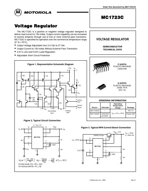
Figure 7. Load Regulation Characteristics With Current Limiting
TA = –55°C RSC = 10 Ω TA = + 25°C TA = + 125°C
–0.3 –0.4 0 20
–0.2
0
5.0
10 15 20 IO, OUTPUT CURRENT (mA)
ELECTRICAL CHARACTERISTICS (TA = +25°C, Vin 12 Vdc, VO = 5.0 Vdc, IL = 1.0 mAdc, RSC = 0, C1 = 100 pF, Cref = 0 and divider
impedance as seen by the error amplifier ≤ 10 kΩ connected as shown in Figure 2, unless otherwise noted.) Characteristics Input Voltage Range Output Voltage Range Input–Output Voltage Differential Reference Voltage Standby Current Drain ( IL = 0, Vin = 30 V) Output Noise Voltage (f = 100 Hz to 10 kHz) Cref = 0 Cref = 5.0 µF Average Temperature Coefficient of Output Voltage (Tlow < TA < Thigh) Line Regulation 12 V < Vin < 15 V 12 V < Vin < 40 V (Tlow < TA < Thigh) 12 V < Vin < 15 V (TA = 25°C) Load Regulation (1.0 mA < IL < 50 mA) TA = 25°C Tlow < TA < Thigh Ripple Rejection (f = 50 Hz to 10 kHz) Cref = 0 Cref = 5.0 µF Short Circuit Current Limit (RSC = 10 Ω, VO = 0) Long Term Stability
MC1374P中文资料

+VCC = 12V C9 0.001
4பைடு நூலகம்
VPin 1 VPin 11
3
t 8 9 10 U1 MC1374 11 12 13 14 C16 47 R8 2.2k R14 56k + R12 180k D2 1N914 C11 22 R7 75Ω 0.22µH L3 C12 47 0.22µH L4 C13 22 R9 560 R11 220 C15 0.001 Output
14 1
P SUFFIX PLASTIC PACKAGE CASE 646
ORDERING INFORMATION
Device MC1374P Operating Temperature Range TA = 0° to +70°C Package Plastic DIP
Figure 1. Simplified Application
ELECTRICAL CHARACTERISTICS (VCC = 12 Vdc, TA = 25°C, fc = 67.25 MHz, Figure 4 circuit, unless otherwise noted.)
Characteristics AM OSCILLATOR/MODULATOR Operating Supply Voltage Supply Current (Figure 1) Video Input Dynamic Range (Sync Amplitude) RF Output (Pin 9, R7 = 75 Ω, No External Load) Carrier Suppression Linearity (75% to 12.5% Carrier, 15 kHz to 3.58 MHz) Differential Gain Distortion (IRE Test Signal) Differential Phase Distortion (3.58 MHz IRE Test Signal) 920 kHz Beat (3.58 MHz @ 30%, 4.5 MHz @ 25%) Video Bandwidth (75 Ω Input Source) Oscillator Frequency Range Internal Resistance across Tank (Pin 6 to Pin 7) Internal Capacitance across Tank (Pin 6 to Pin 7) 5.0 – 0.25 – 36 – 5.0 – – 30 – – – 12 13 1.0 170 40 – 7.0 1.5 –57 – 105 1.8 4.0 12 – 1.0 – – 2.0 10 2.0 – – – – – V mA V Pk mV pp dB % % Degrees dB MHz MHz kΩ pF Min Typ Max Unit
MAX1978中文数据手册

用于Peltier模块的集成温度控制器概论MAX1978 / MAX1979是用于Peltier热电冷却器(TEC)模块的最小, 最安全, 最精确完整的单芯片温度控制器。
片上功率FET和热控制环路电路可最大限度地减少外部元件, 同时保持高效率。
可选择的500kHz / 1MHz开关频率和独特的纹波消除方案可优化元件尺寸和效率, 同时降低噪声。
内部MOSFET的开关速度经过优化, 可降低噪声和EMI。
超低漂移斩波放大器可保持±0.001°C的温度稳定性。
直接控制输出电流而不是电压, 以消除电流浪涌。
独立的加热和冷却电流和电压限制提供最高水平的TEC保护。
MAX1978采用单电源供电, 通过在两个同步降压调节器的输出之间偏置TEC, 提供双极性±3A输出。
真正的双极性操作控制温度, 在低负载电流下没有“死区”或其他非线性。
当设定点非常接近自然操作点时, 控制系统不会捕获, 其中仅需要少量的加热或冷却。
模拟控制信号精确设置TEC 电流。
MAX1979提供高达6A的单极性输出。
提供斩波稳定的仪表放大器和高精度积分放大器, 以创建比例积分(PI)或比例积分微分(PID)控制器。
仪表放大器可以连接外部NTC或PTC热敏电阻, 热电偶或半导体温度传感器。
提供模拟输出以监控TEC温度和电流。
此外, 单独的过热和欠温输出表明当TEC温度超出范围时。
片上电压基准为热敏电阻桥提供偏置。
MAX1978 / MAX1979采用薄型48引脚薄型QFN-EP 封装, 工作在-40°C至+ 85°C温度范围。
采用外露金属焊盘的耐热增强型QFN-EP封装可最大限度地降低工作结温。
评估套件可用于加速设计。
应用光纤激光模块典型工作电路出现在数据手册的最后。
WDM, DWDM激光二极管温度控制光纤网络设备EDFA光放大器电信光纤接口ATE特征♦尺寸最小, 最安全, 最精确完整的单芯片控制器♦片上功率MOSFET-无外部FET♦电路占用面积<0.93in2♦回路高度<3mm♦温度稳定性为0.001°C♦集成精密积分器和斩波稳定运算放大器♦精确, 独立的加热和冷却电流限制♦通过直接控制TEC电流消除浪涌♦可调节差分TEC电压限制♦低纹波和低噪声设计♦TEC电流监视器♦温度监控器♦过温和欠温警报♦双极性±3A输出电流(MAX1978)♦单极性+ 6A输出电流(MAX1979)订购信息* EP =裸焊盘。
MC34072A中文资料
Table 1. Single OpIO (mV) Max TCVIO (µV/°C) (µV/ C) Typ IIO (nA) Max Avol (V/mV) Min BW (Av = 1) (MHz) Typ SR (Av = 1) (V/µs) Typ Supply Voltage (V) Min Max Description
Motorola Master Selection Guide
4.1–1
Analog and Interface Integrated Circuits
元器件交易网
Operational Amplifiers
Motorola offers a broad line of bipolar operational amplifiers to meet a wide range of applications. From low–cost industry–standard types to high precision circuits, the span encompasses a large range of performance capabilities. These Analog integrated circuits are available as single, dual and quad monolithic devices in a variety of temperature ranges and package styles. Most devices may be obtained in unencapsulated ‘‘chip’’ form as well. For price and delivery information on chips, please contact your Motorola Sales Representative or Distributor.
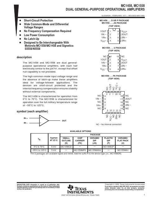
MC1458P中文资料
元器件交易网IMPORTANT NOTICETexas Instruments and its subsidiaries (TI) reserve the right to make changes to their products or to discontinueany product or service without notice, and advise customers to obtain the latest version of relevant informationto verify, before placing orders, that information being relied on is current and complete. All products are soldsubject to the terms and conditions of sale supplied at the time of order acknowledgement, including thosepertaining to warranty, patent infringement, and limitation of liability.TI warrants performance of its semiconductor products to the specifications applicable at the time of sale inaccordance with TI’s standard warranty. Testing and other quality control techniques are utilized to the extentTI deems necessary to support this warranty. Specific testing of all parameters of each device is not necessarilyperformed, except those mandated by government requirements.CERTAIN APPLICATIONS USING SEMICONDUCTOR PRODUCTS MAY INVOLVE POTENTIAL RISKS OFDEATH, PERSONAL INJURY, OR SEVERE PROPERTY OR ENVIRONMENTAL DAMAGE (“CRITICALAPPLICATIONS”). TI SEMICONDUCTOR PRODUCTS ARE NOT DESIGNED, AUTHORIZED, ORWARRANTED TO BE SUITABLE FOR USE IN LIFE-SUPPORT DEVICES OR SYSTEMS OR OTHERCRITICAL APPLICATIONS. INCLUSION OF TI PRODUCTS IN SUCH APPLICATIONS IS UNDERSTOOD TOBE FULLY AT THE CUSTOMER’S RISK.In order to minimize risks associated with the customer’s applications, adequate design and operatingsafeguards must be provided by the customer to minimize inherent or procedural hazards.TI assumes no liability for applications assistance or customer product design. TI does not warrant or representthat any license, either express or implied, is granted under any patent right, copyright, mask work right, or otherintellectual property right of TI covering or relating to any combination, machine, or process in which suchsemiconductor products or services might be or are used. TI’s publication of information regarding any thirdparty’s products or services does not constitute TI’s approval, warranty or endorsement thereof.Copyright © 1999, Texas Instruments Incorporated。
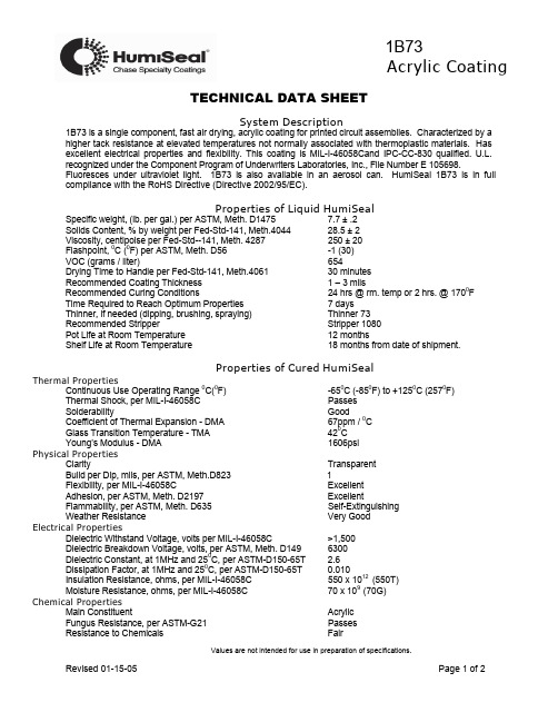
三防胶水
TECHNICAL DATA SHEETSystem Description 1B73 is a single component, fast air drying, acrylic coating for printed circuit assemblies. Characterized by ahigher tack resistance at elevated temperatures not normally associated with thermoplastic materials. Hasexcellent electrical properties and flexibility. This coating is MIL-I-46058Cand IPC-CC-830 qualified. U.L.recognized under the Component Program of Underwriters Laboratories, Inc., File Number E 105698.Fluoresces under ultraviolet light. 1B73 is also available in an aerosol can. HumiSeal 1B73 is in fullcompliance with the RoHS Directive (Directive 2002/95/EC).Properties of Liquid HumiSealSpecific weight, (lb. per gal.) per ASTM, Meth. D1475 7.7 ± .2Solids Content, % by weight per Fed-Std-141, Meth.4044 28.5 ± 2Viscosity, centipoise per Fed-Std--141, Meth. 4287 250 ± 20 Flashpoint, 0C (0F) per ASTM, Meth. D56 -1 (30)VOC (grams / liter) 654Drying Time to Handle per Fed-Std-141, Meth.4061 30 minutesRecommended Coating Thickness 1 – 3 milsRecommended Curing Conditions 24 hrs @ rm. temp or 2 hrs. @ 1700F Time Required to Reach Optimum Properties 7 daysThinner, if needed (dipping, brushing, spraying) Thinner 73Recommended Stripper Stripper 1080Pot Life at Room Temperature 12 monthsShelf Life at Room Temperature 18 months from date of shipment.Properties of Cured HumiSealThermal PropertiesContinuous Use Operating Range 0C(0F) -650C (-850F) to +1250C (2570F)Thermal Shock, per MIL-I-46058C PassesSolderability GoodCoefficient of Thermal Expansion - DMA 67ppm / 0CGlass Transition Temperature - TMA 420CYoung’s Modulus - DMA 1606psiPhysical PropertiesClarity TransparentBuild per Dip, mils, per ASTM, Meth.D823 1Flexibility, per MIL-I-46058C ExcellentAdhesion, per ASTM, Meth. D2197 ExcellentFlammability, per ASTM, Meth. D635 Self-Extinguishing Weather Resistance Very GoodElectrical PropertiesDielectric Withstand Voltage, volts per MIL-I-46058C >1,500Dielectric Breakdown Voltage, volts, per ASTM, Meth. D149 6300 Dielectric Constant, at 1MHz and 250C, per ASTM-D150-65T 2.6 Dissipation Factor, at 1MHz and 250C, per ASTM-D150-65T 0.010Insulation Resistance, ohms, per MIL-I-46058C 550 x 1012 (550T)Moisture Resistance, ohms, per MIL-I-46058C 70 x 109 (70G)Chemical PropertiesMain Constituent AcrylicFungus Resistance, per ASTM-G21 PassesResistance to Chemicals FairValues are not intended for use in preparation of specifications.TECHNICAL DATA SHEETAPPLICATIONCleanliness of the substrate is of extreme importance for the successful application of a conformal coating. Surfaces must be free of moisture, dirt, wax, grease and all other contaminants. Contamination under the coating will cause problems that may lead to assembly failures.HumiSeal coatings may be applied by brush, dip or spray.DippingDepending on the complexity, density and configuration of components on the assembly, it may be necessary to reduce the viscosity of HumiSeal 1B73 with HumiSeal Thinner 73 in order to obtain a uniform film. Once optimum viscosity is determined, a controlled rate of immersion and withdrawal (2 to 6" per minute) will further insure even deposition of the coating and ultimately a uniform film. During the application, evaporation of solvent causes an increase in viscosity that should be adjusted by adding small amounts of Thinner 73. Viscosity in the dip tank should be regularly checked by the use of a simple measuring device such as a Zahn or Ford viscosity cup.SprayingHumiSeal Type 1B73 can be sprayed using conventional spraying equipment. As a rule, the addition of Thinner 73 is necessary to assure a uniform spray pattern resulting in pinhole free film. The amount of thinner and spray pressure will depend on the specific type of spray equipment used. The spraying should be done under an exhaust hood so that the vapor and mist are carried away from the operator. The recommended ratio of HumiSeal Type 1B73 to HumiSeal Thinner 73 is 1 to 1 by volume, as a starting point. The quantities may be adjusted to obtain a uniform coating.BrushingHumiSeal Type 1B73 may be brushed with a small addition of HumiSeal Thinner 73. Uniformity of the film depends on component density and operator's technique.StorageHumiSeal Type 1B73 should be stored at room temperature, away from excessive heat, in tightly closed containers. HumiSeal products may be stored at temperatures of 0-100°F. Avoid direct sunlight. Prior to use, allow the product to equilibrate for 24 hours at 65-90°F.CautionThe solvents in Type 1B73 are flammable. Do not use in presence of open flame or sparks. Avoid inhalation of vapors or spray. Use only in well-ventilated areas. Avoid contact with skin and eyes. If contact occurs, wash with soap and water. If swallowed, call physician immediately. Refer to MSDS before use.All technical data in this bulletin is based on test results and is believed to be correct. However, since the end use of HumiSeal materials (and the mannerof storing and handling them) is beyond our control, we make no warranty-expressed or implied as to the fitness of use, results to be obtained from or effectsof use with respect to these materials. Their use shall be solely by the judgment of and at the risk of the user notwithstanding any statement in thisbulletin. © Copyright 1992 CHASE CORPORATION.HumiSeal Division, Chase Specialty CoatingsPA15238 Pittsburgh,Sales@or412-828-5470Sales:Technical Assistance: 866-932-0800 or TechSupport@。
DS1374中文版
I2C、32位二进制计数器监察RTC的充电器、复位输入/输出总体描述DS1374是设计用来连续用秒计数的32位时钟计数器,是一个附加的计数器来触动一个周期警报器或者是一个看门狗时钟。
如果它损坏了,还可以被用做3字节的稳定的随机存储器。
单独的芯片是用来提供一个在一个四分之一频率下的中断和方波。
精密temperature-compensated参考监控和比较器电路的地位。
停电时,提供了检测输出,并自动复位切换到备用提供必要的时候。
此外,重置密码监测作为一个按钮外部输入为创造一个重置。
该装置编程通过I2C串行地*串口。
应用便携式仪器、销售点设备、医疗设备、电信购买I2C成分的综合生产能力,格言公司,或它的一个sublicensed联营公司,传达出在飞利浦I2C许可专利权使用这些组成部分在一个I2C系统,该系统符合提供I2C规格,定义为飞利浦。
销配置出现在最后的数据表。
特征♦32位二进制计数器第二个二进制计数器♦提供时间刻度等等看门狗定时器,或报警,维迪奇RAM中♦分开的方波输出,中断大头针♦I2C串行接口Power-Fail♦自动检测和开关电路♦Single-Pin重置按钮输入/是开漏重置输出♦低压运行♦Trickle-Charge能力♦-40°C + 85°C操作温度范围♦10-PinμSOP,16-Pin如此♦可在表面贴装包综合晶体(DS1374C)♦保险人(UL)实验室认可典型操作回路未完的指令信息在数据表的最后#代表一个RoHS-compliant装置,包括铅,可以免除RoHS要求下。
铅是JESD97完成范畴e3,并兼容两铅和无铅焊接过程。
* * " # "顶部的地方RoHS-compliant马克表示一个包裹绝对最大额定值推荐直流操作条件(VCC = VCC(MIN)到VCC(最高)、TA = -40°C + 85°C,除非另有注明。
mc1413中文资料

求输出控制隶属度
查表进行模糊推 理,获得模糊输出 输出量解模糊判 决,获得精确的压 缩机转速输出值
返回
PB PM
-6 0 0
-5 0 0
-4 0 0
-3 0 0
-2 0 0
-1 0 0
0 0 0
图5 压缩机转速控制子程序流程图 1 2 3 4 5 6 0 0 0 0.2 0.8 1 0 0.2 0.8 1 0.8 0.2
13
压缩机转速控制如上所述分为三个阶 PID 段开机设定阶段、 模糊逻辑控制阶段、 调节阶段。开机阶段根据系统运行状态确 定压缩机运行转速和持续时间,经过开机 阶段的设定运行判断是进入 PID 调节还是 进入模糊逻辑控制,由温差的大小决定。 当温差在 ± 1.5RC 以内时进入 PID 调节, 反 之进入模糊逻辑控制,如图 5 所示。根据 模糊控制系统的设计方法,首先确定制冷 控制系统的输入输出变量,以系统平均设 定温度与系统实际室内平均温度的偏差, 即系统平均设定温度偏差 ∆T 作为模糊控 制器的一个输入量,以系统平均设定温度 偏差 ∆T 的变化率 ∆T / ∆t 作为另一个输入 量,经过模糊控制器模糊化成为模糊矢量 E 和 EC。而以制冷系统的压缩机转速 Un 作为模糊控制器的输出变量。系统平均设 定温度偏差 ∆T 是指实测被控对象系统的 各室内环境温度值减去设定环境温度值的 差进行加权平均所得的值即为系统平均设 定温差 ∆T 。我们将系统平均设定温差 ∆T 控制范围分为模糊控制区和确定控制区, 以系统平均设定温差 ∆T 值的 ± 1.5R C 为 界。系统平均设定温差 ∆T 值在 ± 1.5 R C 以 外为模糊控制区,以内为确定控制区。在 开机工况完成后的 6 分钟时间内也为模糊 控制区,以利于系统迅速稳定。而在模糊 控制区,将系统平均设定温差 ∆T 分为 7 个模糊状态:PB(正的大 ∆T );PM(正的中 ∆T );PS(正的小 ∆T ) ;Z(正的零 ∆T ) ; NS(负的小 ∆T );NM(负的中 ∆T );NB(负 的大 ∆T )。将系统平均设定温差 ∆T 计算, 圆整, 并将范围大致划分为 13 个点, 分别 给出了它们对 7 个模糊状态的隶属度值, 即输入语言变量的取值:(负大、负中、负 小、零、正小、正中、正大)以符号{NB、 NM、NS、Z、PS、PM、PB}。语言值的 隶属函数选择三角形和梯形, 如表 1 所示。
MC33171-说明书-pdf
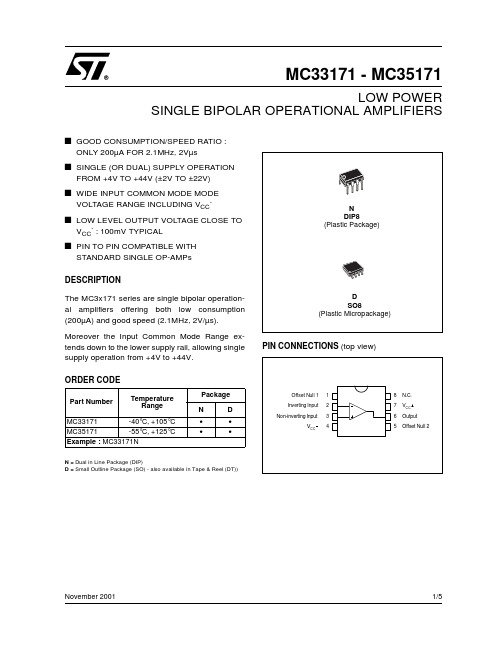
1/5s GOOD CONSUMPTION/SPEED RATIO :ONLY 200µA FOR 2.1MHz, 2Vµss SINGLE (OR DUAL) SUPPLY OPERATIONFROM +4V TO +44V (±2V TO ±22V)s WIDE INPUT COMMON MODE MODEVOLTAGE RANGE INCLUDING V CC -s LOW LEVEL OUTPUT VOLTAGE CLOSE TOV CC - : 100mV TYPICALs PIN TO PIN COMPATIBLE WITHSTANDARD SINGLE OP-AMPs DESCRIPTIONThe MC3x171 series are single bipolar operation-al amplifiers offering both low consumption (200µA) and good speed (2.1MHz, 2V/µs).Moreover the Input Common Mode Range ex-tends down to the lower supply rail, allowing single supply operation from +4V to +44V.ORDER CODEN = Dual in Line Package (DIP)D = Small Outline Package (SO) - also available in Tape & Reel (DT))PIN CONNECTIONS (top view)Part NumberTemperature RangePackage N D MC33171-40°C, +105°C ••MC35171-55°C, +125°C ••Example :MC33171NMC33171 - MC35171LOW POWERSINGLE BIPOLAR OPERATIONAL AMPLIFIERSNovember 2001MC33171-MC351712/5SCHEMATIC DIAGRAMINPUT OFFSET VOLTAGE NULL CIRCUITMAXIMUM RATINGSOPERATING CONDITIONSSymbol ParameterValue Unit V CC Supply Voltage±22V V id Differential Input Voltagesee note 1)1.Either or both input voltages must not exceed the magnitude of Vcc.V V i Input Voltagesee note 1V Output Short Circuit DurationIndefinite s T oper Operating Free-Air Temperature range MC33171 MC35171-40 to 105-55 to 125°C T j Junction Temperature 150°C T stgStorage Temperature-65 to 150°CSymbol ParameterValue Unit V CCSupply Voltage±2 to ±22VMC33171-MC351713/5ELECTRICAL CHARACTERISTICSV CC + = +15V, V CC - = -15V, R L connected to Ground, T amb = 25°C (unless otherwise specified)SymbolParameterMin.Typ.Max.UnitV io Input Offset VoltageV CC + = +15V, V CC - = -15V, V ic = 0VV CC + = 5V, V CC - = 0V, V ic = 0V, V o = 1.4VV CC + = +15V, V CC - = -15V, V ic = 0V, T min. ≤ T amb ≤ T max .11 4.556.5mV DV io Input Offset Voltage Drift 10µV/°C I io Input Offset Current (V ic = 0V)T min . ≤ T amb ≤ T max.52040nA I ib Input Bias Current (V ic = 0V) T min . ≤ T amb ≤ T max.20100200nA A vdLarge Signal Voltage Gain (R L = 10k Ω, V o = ±10V)T min . ≤ T amb ≤ T max.5025100V/mVV OHHigh Level Output VoltageV CC + = 5V, V CC - = 0V, R L = 10k ΩV CC + = +15V, V CC - = -15V, R L = 10k ΩV CC + = +15V, V CC - = -15V, R L = 10k Ω, T min. ≤ T amb ≤ T max . 3.513.613.3 4.214.2VV OLLow Level Output VoltageV CC + = 5V, V CC - = 0V, R L = 10k ΩV CC + = +15V, V CC - = -15V, R L = 10k ΩV CC + = +15V, V CC - = -15V, R L = 10k Ω, T min. ≤ T amb ≤ T max .0.1-140.15-13.6-13.3VI sc Output Short Circuit Current (V id = ±1V, V o = 0V)Source Sink 315627mAV icm Input Common Mode Voltage Range T min . ≤ T amb ≤ T maxV CC - to V CC + - 1.8)V CC - to (V CC + - 2.2)V CMR Common-mode Rejection Ratio (V ic = V icm min.)80100dB SVR Supply Voltage Rejection Ratio (V CC = ±5 to ±15V)80100dB I CC Supply CurrentV CC + = 5V, V CC - = 0V, no loadV CC + = +15V, V CC - = -15V, no loadV CC + = +15V, V CC - = -15V no load, T min. ≤ T amb ≤ T max .200220250250300µA SR Slew Rate (V i = ±10V, R L = 10k Ω, C L = 100pF) 1.62V/µs GBP Gain Bandwidth ProductR L = 10k Ω, C L = 100pF, f = 100kHz 1.4 2.1MHz φm Phase Margin (R L = 10k Ω, C L = 100pF)45Degrees e n Equivalent Input Noise Voltage (f = 1kHz)29THDTotal Harmonic Distortion0.05%nV Hz -----------MC33171-MC351714/5PACKAGE MECHANICAL DATA 8 PINS - PLASTIC DIPDimensionsMillimetersInches Min.Typ.Max.Min.Typ.Max.A 3.320.131a10.510.020B 1.15 1.650.0450.065b 0.3560.550.0140.022b10.2040.3040.0080.012D 10.920.430E 7.959.750.3130.384e 2.540.100e37.620.300e47.620.300F 6.60260i 5.080.200L 3.18 3.810.1250.150Z1.520.060MC33171-MC351715/5PACKAGE MECHANICAL DATA8 PINS - PLASTIC MICROPACKAGE (SO)DimensionsMillimetersInches Min.Typ.Max.Min.Typ.Max.A 1.750.069a10.10.250.0040.010a2 1.650.065a30.650.850.0260.033b 0.350.480.0140.019b10.190.250.0070.010C 0.250.50.0100.020c145° (typ.)D 4.8 5.00.1890.197E 5.86.20.2280.244e 1.270.050e3 3.810.150F 3.8 4.00.1500.157L 0.41.270.0160.050M 0.60.024S8° (max.)Information furnished is believed to be accurate and reliable. However, STMicroelectronics assumes no responsibility for the consequences of use of such information nor for any infringement of patents or other rights of third parties which may result from its use. No license is granted by implication or otherwise under any patent or patent rights of STMicroelectronics. Specifications mentioned in this publication are subject to change without notice. This publication supersedes and replaces all information previously supplied. STMicroelectronics products are not authorized for use as critical components in life support devices or systems without express written approval of STMicroelectronics.© The ST logo is a registered trademark of STMicroelectronics© 2001 STMicroelectronics - Printed in Italy - All Rights ReservedSTMicroelectronics GROUP OF COMPANIESAustralia - Brazil - Canada - China - Finland - France - Germany - Hong Kong - India - Israel - Italy - Japan - MalaysiaMalta - Morocco - Singapore - Spain - Sweden - Switzerland - United Kingdom - United States© 。
在音响电源设计中使用MC1723C电压调节器芯片
在音响电源设计中使用MC1723C电压调节器芯片【摘要】MC1723C是一款常用的电压调节器芯片,具有稳定性高、电流输出能力强等特点。
在音响电源设计中,MC1723C扮演着重要的角色,可以提供稳定的电压输出,保证音响设备的正常运行。
本文介绍了MC1723C的特点、应用、工作原理以及与其他调节器芯片的比较,阐述了MC1723C在音响电源设计中的优势,展望了其未来发展。
结合MC1723C在音响电源设计中的重要性,总结了它在提升音响设备性能和稳定性方面的价值。
通过深入研究MC1723C的特性和应用,可以更好地理解和应用这一芯片,为音响电源设计提供更好的解决方案。
【关键词】MC1723C, 电压调节器芯片, 音响电源设计, 特点, 应用, 工作原理, 比较, 优势, 未来发展, 重要性, 价值.1. 引言1.1 介绍MC1723C电压调节器芯片MC1723C是一款高性能的电压调节器芯片,广泛应用于各种电子设备中。
它能够稳定输出电压,在电路中起到稳压作用,保证电子设备的正常运行。
MC1723C具有高输出电流能力和较低的输出纹波,能够提供稳定且清洁的电源供电。
它还具有过电流保护和过热保护功能,可有效保护电子设备和电源系统。
MC1723C采用双输入电压供电,有较宽的输入电压范围和良好的稳定性,适用于各种复杂的电子设备设计。
1.2 音响电源设计的重要性音响电源设计在音频设备的整体性能中起着至关重要的作用。
一个优秀的音响电源设计可以为音频设备提供稳定可靠的电源供应,有效降低噪音和失真,并提高音频信号的清晰度和保真度。
合理设计的音响电源还可以延长音频设备的使用寿命,提高其整体可靠性和稳定性。
在音响系统中,电源对音质的影响非常显著,一个稳定而干净的电源可以确保音频信号的准确传输和还原,使得音频听感更加真实自然。
在音响设备设计中,必须高度重视音响电源的设计,选择合适的电压调节器芯片如MC1723C来确保电源供应的稳定性和可靠性。
MC1413P
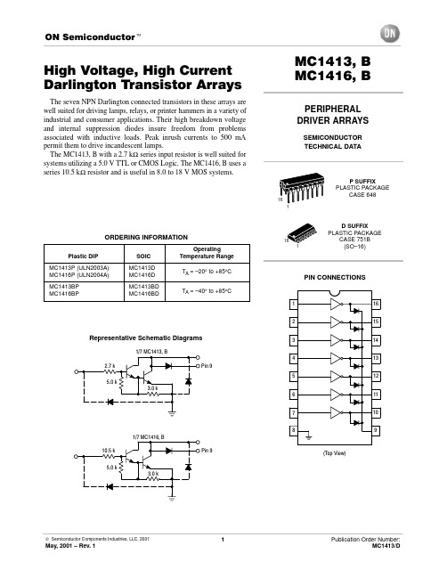
High Voltage, High Current Darlington Transistor ArraysThe seven NPN Darlington connected transistors in these arrays are well suited for driving lamps, relays, or printer hammers in a variety of industrial and consumer applications. Their high breakdown voltage and internal suppression diodes insure freedom from problems associated with inductive loads. Peak inrush currents to 500 mA permit them to drive incandescent lamps.The MC1413, B with a 2.7 k Ω series input resistor is well suited for systems utilizing a 5.0 V TTL or CMOS Logic. The MC1416, B uses a series 10.5 k Ω resistor and is useful in 8.0 to 18 V MOS systems.ORDERING INFORMATIONRepresentative Schematic DiagramsPin 9Pin 9MAXIMUM RATINGS (T= 25°C, and rating apply to any one device in the package, unless otherwise noted.)ELECTRICAL CHARACTERISTICS (T= 25°C, unless otherwise noted)% DUTY CYCLEV I , INPUT VOLTAGE (V)0100200400300500700600800I C , C O L L E C T O R C U R R E N T (m A )I I , I N P U T C U R R E N T (m A )N U M B E R O F D R I V E R S U S E D100400300200I I , INPUT CURRENT (µA)I O , O U T P U T C U R R E N T (m A )TYPICAL PERFORMANCE CURVES – T A = 25°CV I , INPUT VOLTAGE (V)I O , O U T P U T C U R R E N T (m A )Figure 1. Output Current versus Input VoltageFigure 2. Output Current versus Input CurrentFigure 5. Input Characteristics – MC1416, BFigure 6. Maximum Collector Currentversus Duty Cycle(and Number of Drivers in Use)NOTES:1.DIMENSIONING AND TOLERANCING PER ANSI Y14.5M, 1982.2.CONTROLLING DIMENSION: INCH.3.DIMENSION L TO CENTER OF LEADS WHEN FORMED PARALLEL.4.DIMENSION B DOES NOT INCLUDE MOLD FLASH.5.ROUNDED CORNERS OPTIONAL.MDIM MIN MAX MIN MAX MILLIMETERSINCHES A 0.7400.77018.8019.55B 0.2500.270 6.35 6.85C 0.1450.175 3.69 4.44D 0.0150.0210.390.53F 0.0400.70 1.02 1.77G 0.100 BSC 2.54 BSC H 0.050 BSC 1.27 BSC J 0.0080.0150.210.38K 0.1100.130 2.80 3.30L 0.2950.3057.507.74M 0 10 0 10 S0.0200.0400.51 1.01____P SUFFIXPLASTIC PACKAGE CASE 648–08ISSUE RNOTES:1.DIMENSIONING AND TOLERANCING PER ANSI Y14.5M, 1982.2.CONTROLLING DIMENSION: MILLIMETER.3.DIMENSIONS A AND B DO NOT INCLUDE MOLD PROTRUSION.4.MAXIMUM MOLD PROTRUSION 0.15 (0.006)PER SIDE.5.DIMENSION D DOES NOT INCLUDE DAMBAR PROTRUSION. ALLOWABLE DAMBARPROTRUSION SHALL BE 0.127 (0.005) TOTAL IN EXCESS OF THE D DIMENSION AT MAXIMUM MATERIAL CONDITION.SBM0.25 (0.010)AST DIM MIN MAX MIN MAX INCHESMILLIMETERS A 9.8010.000.3860.393B 3.80 4.000.1500.157C 1.35 1.750.0540.068D 0.350.490.0140.019F 0.40 1.250.0160.049G 1.27 BSC 0.050 BSC J 0.190.250.0080.009K 0.100.250.0040.009M 0 7 0 7 P 5.80 6.200.2290.244R0.250.500.0100.019____D SUFFIXPLASTIC PACKAGE CASE 751B–05(SO–16)ISSUE JON Semiconductor and are trademarks of Semiconductor Components Industries, LLC (SCILLC). SCILLC reserves the right to make changes without further notice to any products herein. SCILLC makes no warranty, representation or guarantee regarding the suitability of its products for any particular purpose, nor does SCILLC assume any liability arising out of the application or use of any product or circuit, and specifically disclaims any and all liability, including without limitation special, consequential or incidental damages. “Typical” parameters which may be provided in SCILLC data sheets and/or specifications can and do vary in different applications and actual performance may vary over time. All operating parameters, including “Typicals” must be validated for each customer application by customer’s technical experts. SCILLC does not convey any license under its patent rights nor the rights of others.SCILLC products are not designed, intended, or authorized for use as components in systems intended for surgical implant into the body, or other applications intended to support or sustain life, or for any other application in which the failure of the SCILLC product could create a situation where personal injury or death may occur. Should Buyer purchase or use SCILLC products for any such unintended or unauthorized application, Buyer shall indemnify and hold SCILLC and its officers, employees, subsidiaries, affiliates, and distributors harmless against all claims, costs, damages, and expenses, and reasonable attorney fees arising out of, directly or indirectly, any claim of personal injury or death associated with such unintended or unauthorized use, even if such claim alleges that SCILLC was negligent regarding the design or manufacture of the part. SCILLC is an Equal Opportunity/Affirmative Action Employer. PUBLICATION ORDERING INFORMATIONCENTRAL/SOUTH AMERICA:Spanish Phone:303–308–7143 (Mon–Fri 8:00am to 5:00pm MST)Email:ONlit–spanish@Toll–Free from Mexico: Dial 01–800–288–2872 for Access –then Dial 866–297–9322ASIA/PACIFIC: LDC for ON Semiconductor – Asia SupportPhone:1–303–675–2121 (Tue–Fri 9:00am to 1:00pm, Hong Kong Time)Toll Free from Hong Kong & Singapore:001–800–4422–3781Email: ONlit–asia@JAPAN: ON Semiconductor, Japan Customer Focus Center4–32–1 Nishi–Gotanda, Shinagawa–ku, Tokyo, Japan 141–0031Phone: 81–3–5740–2700。
主控,置位与复位指令

Y0
时序图
12
4.2.8 置位与复位指令(SET、RET)
置位指令与复位指令使用次数说明
X0 SET Y0
LD SET LD RET
X0 Y0 X1 Y0 指令表程序
X1 RST Y0
梯形图
X0
X1
对同一编程元件,可多次使用SET 和RST指令。SET与RST指令之间可以 插入别的程序。
Y0
时序图
(2)切断某些电路; (3)变换先前的电路。 在执行程序全清操作后,全部指令都变成NOP。
25
4.2.10 空操作指令(N0P)
短路某些接点或电路,如( a )、( b )所示;
切断某些电路,如( c )、( d )所示;
变换先前的电路,如( e )所示。
26
4.2.11 程序结束指令(END)
左重右轻,上重下轻,多上,串左
40
4.3.1 画梯形图的规则和技巧
二、编程的技巧
1、采用合理的编程顺序和适当的电路变换,尽量减少程序步数,以 节省内存空间和缩短扫描时间
⑴、并联电路上下位置可调,应将单个触点的支路放下面。
X0 Y0 X1 X2
ORB
X1
X2
Y0
X0
不好! 0 1 2 3 4 LD LD AND ORB OUT X0 X1 X2 Y0 0 1 2 3 LD AND OR OUT
编程举例
时序图
22
4.2.9 脉冲指令(PLS、PLF)
使用注意:
• 使用这2条指令时,要注意目标元件。在满 足执行条件(X0=ON),PLC由运行-停止运行时,PLS M0动作,但是PLS M500 (断电时有后备电池的辅助继电器)不动 作。这是因为M500是特殊保持继电器,即 使在断电停电时其动作也能保持。
- 1、下载文档前请自行甄别文档内容的完整性,平台不提供额外的编辑、内容补充、找答案等附加服务。
- 2、"仅部分预览"的文档,不可在线预览部分如存在完整性等问题,可反馈申请退款(可完整预览的文档不适用该条件!)。
- 3、如文档侵犯您的权益,请联系客服反馈,我们会尽快为您处理(人工客服工作时间:9:00-18:30)。
+VCC = 12V C9 0.001
4
VPin 1 VPin 11
3
t 8 9 10 U1 MC1374 11 12 13 14 C16 47 R8 2.2k R14 56k + R12 180k D2 1N914 C11 22 R7 75Ω 0.22µH L3 C12 47 0.22µH L4 C13 22 R9 560 R11 220 C15 0.001 Output
V Channel 3 + R1 470 C1 0.001 R3 470 L1 R2 470 + + C4 50 C3 120 5–25 C7 C2 56 4 + C8 0.001 S1 R10 10k D1 MPN3404 7 6 5 4 C14 0.01 3 2 C5 0.001 R5 3.3k R6 2.2k Shaded Parts Optional L1 – 4 Turns #22, 1/4″ Dia. L2 – 40 Turns, #36, 3/16″ Dia.
14 1
P SUFFIX PLASTIC PACKAGE CASE 646
ORDERING INFORMATION
Device MC1374P Operating Temperature Range TA = 0° to +70°C Package Plastic DIP
Figure 1. Simplified Application
%
kΩ pF pF kΩ
2
MOTOROLA ANALOG IC DEVICE DATA
元器件交易网
MC1374
Figure 2. TV Modulator
Bias Section
FM Oscillator/Modulator Sound Carrier Audio In OSC B+ 14 4
Q25 Q24
Q23
Q26
Q27
Q8
Q9
Q16
Q17
Q18
I1 = 1.15 mA
I1 = 1.15 mA
D1 R1 5 Gnd R2 R3 R4 R5 1 Sound Carrier In
R6 12 Gain
R7
R8
I2 = 1.15 mAeo In
GENERAL INFORMATION
ELECTRICAL CHARACTERISTICS (VCC = 12 Vdc, TA = 25°C, fc = 67.25 MHz, Figure 4 circuit, unless otherwise noted.)
Characteristics AM OSCILLATOR/MODULATOR Operating Supply Voltage Supply Current (Figure 1) Video Input Dynamic Range (Sync Amplitude) RF Output (Pin 9, R7 = 75 Ω, No External Load) Carrier Suppression Linearity (75% to 12.5% Carrier, 15 kHz to 3.58 MHz) Differential Gain Distortion (IRE Test Signal) Differential Phase Distortion (3.58 MHz IRE Test Signal) 920 kHz Beat (3.58 MHz @ 30%, 4.5 MHz @ 25%) Video Bandwidth (75 Ω Input Source) Oscillator Frequency Range Internal Resistance across Tank (Pin 6 to Pin 7) Internal Capacitance across Tank (Pin 6 to Pin 7) 5.0 – 0.25 – 36 – 5.0 – – 30 – – – 12 13 1.0 170 40 – 7.0 1.5 –57 – 105 1.8 4.0 12 – 1.0 – – 2.0 10 2.0 – – – – – V mA V Pk mV pp dB % % Degrees dB MHz MHz kΩ pF Min Typ Max Unit
AM Modulator Sound Carrier Oscillator 3 2 VCC 8 RF Out 9
AM Oscillator RF Tank 7 6
R10
R11
R12 6.0k
R16 Q7 Q1 R13 325 Q12 Q13 Q14 Q15 R17 C1 R14 Q3 Q4 R15 Q5 Q6 Q10 Q11 Q2 Q19 Q20 Q21 Q22
MC1374
TV MODULATOR CIRCUIT
SEMICONDUCTOR TECHNICAL DATA
• • • • • • •
Channel 3 or 4 Operation Variable Gain RF Modulator Wide Dynamic Range Low Intermodulation Distortion Positive or Negative Sync Low Audio Distortion Few External Components
Rating Supply Voltage Operating Ambient Temperature Range Storage Temperature Range Junction Temperature Power Dissipation Package Derate above 25°C Value 14 0 to +70 –65 to +150 150 1.25 10 mW/°C Unit Vdc °C °C °C W
+
R4 6.8k
L2
C10 10µF +
Video In Audio In
1
R13 30k
C6 1µF
Rev 0
MOTOROLA ANALOG IC DEVICE DATA
1
元器件交易网
MC1374
MAXIMUM RATINGS (TA = 25°C, unless otherwise noted.)
ELECTRICAL CHARACTERISTICS (TA = 25°C, VCC = 12 Vdc, 4.5 MHz, Test circuit of Figure 11, unless otherwise noted.)
Characteristics FM OSCILLATOR/MODULATOR Frequency Range of Modulator Frequency Shift versus Temperature (Pin 14 open) Frequency Shift versus VCC (Pin 14 open) Output Amplitude (Pin 3 not loaded) Output Harmonics, Unmodulated Modulation Sensitivity 1.7 MHz 4.5 MHz 10.7 MHz 14 – – – – – – – – – – – – – – 4.5 0.2 – 900 – 0.20 0.24 0.80 0.6 1.4 2.0 6.0 5.0 5.0 2.0 14 0.3 4.0 – –40 – – – 1.0 – – – – – – MHz kHz/°C kHz/V mVpp dB MHz/V Min Typ Max Unit
Audio Distortion (±25 kHz Deviation, Optimized Bias Pin 14) Audio Distortion (±25 kHz Deviation, Pin 14 self biased) Incidental AM (±25 kHz FM) Audio Input Resistance (Pin 14 to ground) Audio Input Capacitance (Pin 14 to ground) Stray Tuning Capacitance (Pin 3 to ground) Effective Oscillator Source Impedance (Pin 3 to load)
元器件交易网
Order this document by MC1374/D
TV Modulator Circuit
The MC1374 includes an FM audio modulator, sound carrier oscillator, RF oscillator, and RF dual input modulator. It is designed to generate a TV signal from audio and video inputs. The MC1374’s wide dynamic range and low distortion audio make it particularly well suited for applications such as video tape recorders, video disc players, TV games and subscription decoders. • Single Supply, 5.0 V to 12 V
The MC1374 contains an RF oscillator, RF modulator, and a phase shift type FM modulator, arranged to permit good printed circuit layout of a complete TV modulation system. The RF oscillator is similar to the one used in MC1373, and is coupled internally in the same way. Its frequency is controlled by an external tank on Pins 6 and 7, or by a crystal circuit, and will operate to approximately 105 MHz. The video modulator is a balanced type as used in the well known MC1496. Modulated sound carrier and composite video information can be put in separately on Pins 1 and 11 to minimize unwanted crosstalk. A single resistor on Pins 12 and 13 is selected to set the modulator gain. The RF output at Pin 9 is a current source which drives a load connected from Pin 9 to VCC. The FM system was designed specifically for the TV intercarrier function. For circuit economy, one phase shift circuit was built into the ship. Still, it will operate from 1.4 MHz to 14 MHz, low enough to be used in a cordless telephone base station (1.76 MHz), and high enough to be used as an FM IF test signal source (10.7 MHz). At 4.5 MHz, a deviation of ± 25 kHz can be achieved with 0.6% distortion (typical). In the circuit above, devices Q1 through Q7 are active in the oscillator function. Differential amplifier Q3, Q4, Q5, and Q6 acts as a gain stage, sinking current from input section Q1, Q2 and the phase shift network R17, C1. Input amplifier Q1, Q2 can vary the amount of “in phase” Q4 current to be combined with phase shifter current in load resistor R16. The R16 voltage is applied to emitter follower Q7 which drives an external L–C circuit. Feedback from the center of the L–C circuit back to the base of Q6 closes the loop. As audio input is applied which would offset the stable oscillatory phase, the frequency changes to counteract. The input to Pin 14 can include a dc feedback current for AFC over a limited range. The modulated FM signal from Pin 3 is coupled to Pin 1 of the RF modulator and is then modulated onto the AM carrier.
