Electronic structures of layered perovskite Sr2MO4 (M=Ru, Rh, and Ir)
高政祥固体物理讲义
a1
=
a 2
(
i
+
j
−
k)
a2
=
a(
2
j+k −i)
a3
=
a 2
(
k
+
i
−
j)
1
面心立方晶格的原胞和基矢
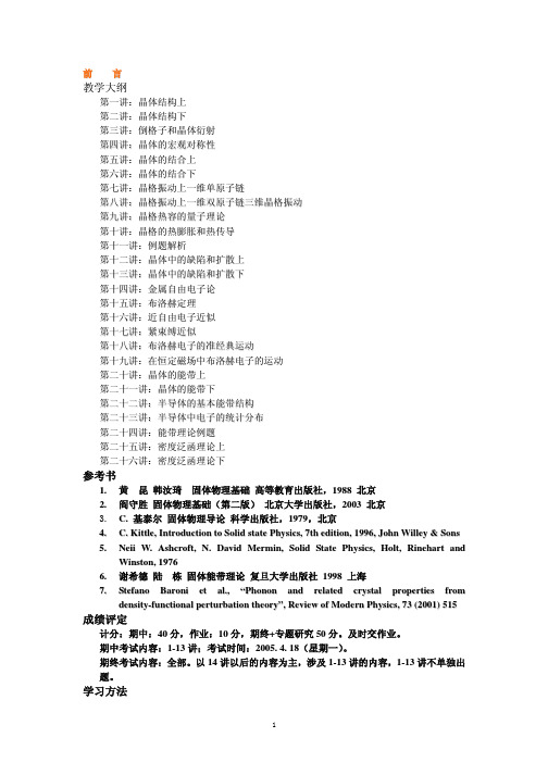
在面心立方晶格中,通常由一个立方顶点到三个相邻的面心的矢量作为晶格基矢:
a1
=
a 2
(
i
+
j)
a2
=
a(
2
j + k)
a3
=
a 2
(
k
+
i)
Wigner-Seitz 原胞
作由晶格原点出发的所有晶格矢量的垂直平分面,这些垂直平分面所封闭的包含晶格原点的 最小空间,称为 Wigner-Seitz 原胞。
例题 1.3
在六方晶体中,晶面常用四个指数 (hkil) 表示,它们代表一个晶面在六角形平面基矢 a 1, a 2, a 3 (两两夹角为 120°)轴上的截距为 a1/h, a2/k, a 3/i 的整数倍,在六次轴 c 上的截距为 c/l 的整 数倍。证明: h + k + i = 0。 证明:考虑离原点最近的晶面,在六角形平面基矢 a1, a2, a3 (两两夹角为 120°)轴上的截距为 a1/h, a2/k, a3/i。则矢量 a1/h − a2/k 和矢量 a2/k − a3/i 共线,即(a1/h − a2/k)×(a2/k − a3/i) = 0
3
第二讲:晶体结构下
晶系
如果要具有一定的宏观对称性(32 个点群对称性),晶体单胞轴矢 a, b, c 必须满足怎样的
2012-半导体物理-8-异质结-2014-05-28解析

突变异质结:从一种半导体材料向另一种半导体材料的过 渡发生在几个原子间距的范围内。
pn结的能带图 qVD E Fn E Fp
突变反型异质结的能带图
形成异质结时电子从n型半导体流向p型半导体,空穴的流动方向相反。 达到平衡时,两块半导体具有统一的费米能级。
在异质结界面的两边形成空间电荷区,产生内建电场和附加电势能,使空间电 荷区中的能带发生弯曲。
qVD = qVD1 + qVD2 = EF2 - EF1 = W1 - W2
Group B
1. 1 2. 2 3. 5
Group C
1. 1 2. 2 3. 5
半导体物理学
第7章 金属和半导体的接触子阱中二维电子气的形成及其电子能态
波函数满足的薛定谔方程: 波函数分离变量: 波函数分离变量:
面内波函数:
电子能量:
界面量子阱中二维电子气的势阱和状态密度
二维电子气的状态密度
电子的能量: k空间原胞的面积:
k空间k-k+dk圆环的面积: E-k关系: 状态密度:
低维半导体材料及其状态密度
半导体超晶格
• 由于迷你带的形成,超晶格的发光波长相对于量子阱的发光波长发生 一个红移。
• 在I型超晶格中,电子和空穴被束缚在同种材料中。 • 在II型超晶格中,电子和空穴被束缚在不同材料中。
半导体激光器
单异质结激光器
• 时间:1969年第一次制成。 • 方法:液相外延。 • 结构:在GaAs pn结上再生长一层p型AlGaAs. • 优点:阈值低,效率高。 • 阈值电流密度:10-15 103 A/cm2,小于同质结激光器。 • 原因:注入的电子和空穴被阻挡在p型GaAs中复合;激光也限制在其中。
2.3埃伯尔斯-莫尔模型_《电子线路(线性部分)》第四版课件

VBE VT
1 ) R IC
VBC VT
同理: 式中
I C F I E I CBO (e
1 )
I CBO ( 1 R F)I CBS
I E I EBO (e
VBE VT
1 ) R IC
VBC VT
根据方程组
I C F I E I CBO (e
第三节
埃伯尔斯
—————— 莫尔模型
埃伯尔斯——莫尔模型:是晶体三极管的通用模型, 适用于各种工作模式。 设 晶体三极管处于饱和模式时,两个结均加正偏。 根据第二节的分析可知: IF 为发射结的正向偏置电流; IR 为集电结的正向偏置电流。 它们与结电压之间均满足指数关系:
VBE VT
I F I EBS (e
I R I CBS (e
1 )
将其代如下式
VBC VT
1 )
I E I F R IR
IC F I F I R
则 晶体三极管的 IE 与 IC 可分别表示为:
VBE VT VBC VT
I E I EBS (e
1 ) R I CBS (e
VBE VT
1 )
I C F I EBS (e
IE
VBE VT
1) (1 R)I CBS (e
IC
C
1)
IF
E
RIR
B
IB
I E I EBS (e
VBE VT
1 ) R I CBS (e
VBE VT
VBC VT
VBC VT
1 )
1 )
I E I F R IR
裴攀-翻译中文
第6章光源和放大器在光纤系统,光纤光源产生的光束携带的信息。
激光二极管和发光二极管是两种最常见的来源。
他们的微小尺寸与小直径的光纤兼容,其坚固的结构和低功耗要求与现代的固态电子兼容。
在以下几个GHz的工作系统,大部分(或数Gb /秒),信息贴到光束通过调节输入电流源。
外部调制(在第4、10章讨论)被认为是当这些率超标。
我们二极管LED和激光研究,包括操作方法,转移特性和调制。
我们计划以获得其他好的或理念的差异的两个来源,什么情况下调用。
当纤维损失导致信号功率低于要求的水平,光放大器都需要增强信号到有效的水平。
通过他们的使用,光纤链路可以延长。
因为光源和光放大器,如此多的共同点,他们都是在这一章处理。
1.发光二极管一个发光二极管[1,2]是一个PN结的半导体发光时正向偏置。
图6.1显示的连接器件、电路符号,能量块和二极管关联。
能带理论提供了对一个)简单的解释半导体发射器(和探测器)。
允许能带通过的是工作组,其显示的宽度能在图中,相隔一禁止区域(带隙)。
在上层能带称为导带,电子不一定要到移动单个原子都是免费的。
洞中有一个正电荷。
它们存在于原子电子的地点已经从一个中立带走,留下的电荷原子与净正。
自由电子与空穴重新结合可以,返回的中性原子状态。
能量被释放时,发生这种情况。
一个n -型半导体拥有自由电子数,如图图英寸6.1。
p型半导体有孔数自由。
当一种P型和一种N型材料费米能级(WF)的P和N的材料一致,并外加电压上作用时,产生的能垒如显示的数字所示。
重参杂材料,这种情况提供许多电子传到和过程中需要排放的孔。
在图中,电子能量增加垂直向上,能增加洞垂直向下。
因此,在N地区的自由电子没有足够的能量去穿越阻碍而移动到P区。
同样,空穴缺乏足够的能量克服障碍而移动进入n区。
当没有外加电压时,由于两种材料不同的费米能级产生的的能量阻碍,就不能自由移动。
外加电压通过升高的N端势能,降低一侧的P端势能,从而是阻碍减小。
如果供电电压(电子伏特)与能级(工作组)相同,自由电子和自由空穴就有足够的能量移动到交界区,如底部的数字显示,当一个自由电子在交界区遇到了一个空穴,电子可以下降到价带,并与空穴重组。
AlGaN-GaN高电子迁移率晶体管模型、关键工艺及器件制作

AlGaN-GaN高电子迁移率晶体管模型、关键工艺及器件制作AlGaN/GaN高电子迁移率晶体管模型、关键工艺及器件制作近年来,随着宽禁带半导体材料的发展, AlGaN/GaN 高电子迁移率晶体管 (HEMT) 在射频功率放大器、微波开关、高频通信等领域中起着重要作用。
本文将重点介绍 AlGaN/GaN HEMT 的模型、关键工艺及器件制作,并探讨其在射频功率放大器中的应用。
AlGaN/GaN HEMT 的模型是研究和设计该器件的基础。
一种常用的 HEMT 模型是 Hockfield 模型,它基于输运理论和二维电子气的特性。
该模型通过考虑电子在AlGaN/GaN异质结构中的构建状态和电缺陷等因素,能够精确描述 HEMT 的输运性能。
关键工艺对 AlGaN/GaN HEMT 的性能和稳定性具有重要影响。
其中最核心的是高电子迁移率材料的外延生长技术。
通常使用金属有机化学气相沉积 (MOCVD) 方法,通过在晶体表面沉积 GaN 和 AlGaN 薄膜来制备 AlGaN/GaN HEMT 结构。
在外延生长过程中,控制好材料的复合级别、晶格匹配度和材料质量非常关键。
器件制作也是实现高性能 AlGaN/GaN HEMT 的关键步骤。
一般的制作流程包括制备衬底材料、生长材料、光刻、腐蚀、金属化处理等。
在制备过程中,需要严格控制温度、厚度和压力等参数,以确保器件的质量和稳定性。
AlGaN/GaN HEMT 在射频功率放大器领域具有广泛的应用。
射频功率放大器可以将来自信号发生器的低功率信号放大到高功率,用于无线通信系统等。
相比传统的功率放大器,AlGaN/GaN HEMT 具有更高的开关速度和更低的损耗,使得其具备更高的工作频率和更高的效率。
然而, AlGaN/GaN HEMT 在应用过程中也面临一些挑战。
其中之一是高功率密度下的热管理问题。
由于 AlGaN/GaN HEMT 在高功率工作时会产生大量的热量,因此需要采用有效的散热技术,以确保器件的稳定性和可靠性。
范德瓦尔相互作用采取atom-based方法处理
范德瓦尔相互作用采取atom-based方法处理社会物理学中,范德瓦尔相互作用被认为是自然界中的一种势能,它是由于相邻分子之间的极化和磁化而产生的相互作用。
原子之间相互作用是研究分子和固体性质的基础,同时也是许多现代技术的基础。
目前,处理范德瓦尔相互作用的方法主要有两种,分别是基于能量的方法和基于原子的方法。
基于能量的方法是研究范德瓦尔相互作用的传统方法,它基于二体范德瓦尔解析式,将分子作为两体问题处理,并利用公式计算其势能。
这种方法的优点是计算简单,能够处理大型分子和高密度系统。
但是,这种方法的局限性在于它无法处理特殊性质,比如极化和双极分子相互作用,以及长程效应和晶体环境中的相互作用。
基于原子的方法则是新近发展起来的处理范德瓦尔相互作用的方法。
它将范德瓦尔相互作用看作原子之间的相互作用,并基于该原则建立了一种新的计算方法,即地毯式计算法。
这种方法的特点是注重原子之间的相互作用,利用原子之间的感应极化和互感应作用共同处理相邻原子之间的相互作用,得到了比较准确的结果。
地毯式计算法的核心思想是将分子表面覆盖成一张无数细小区域的地毯,每一小块地毯的大小都是一个原子的大小。
当计算相互作用时,先确定两个原子之间的位置关系,然后确定相邻原子之间的相互作用。
如果两个原子间的距离很大,相互作用被认为很小,可以忽略不计。
但是,当两个原子距离很近时,相互作用将是很强烈的,可通过一种数学方法计算得出。
在整个计算中,每个原子的电子云都被视为等同的,以简化计算。
总之,地毯式计算法是目前范德瓦尔相互作用研究中的新技术,它的发展为分子动力学和分子机器的研究提供了新思路和新方法,对于理解范德瓦尔相互作用具有重要意义。
诺贝尔奖中的材料学

结构
理论上,有三种准晶模型。 理论上,有三种准晶模型。 第一种即是彭罗斯模型 两种或两种以上的 种即是彭罗斯模型: 第一种即是彭罗斯模型:两种或两种以上的 晶胞以特定规则拼接在一起铺满平面; 晶胞以特定规则拼接在一起铺满平面; 第二种是玻璃模型:子簇可以较为随机地加 第二种是玻璃模型:子簇可以较为随机地加 种是玻璃模型 入交互形成; 入交互形成; 第三种是随机平铺模型: 种是随机平铺模型 第三种是随机平铺模型:它结合了前两种的 特点, 特点,即彭罗斯模型中的规则不必被严格执 只要结构中并没有出现间隙, 行,只要结构中并没有出现间隙,晶胞自行 加以组合即可。 加以组合即可。
The End
Thanks For Your Attention
发现简史
1982年 1982年4月8日,以色列化学家谢赫特曼在铝 锰合金冷冻固化实验中首次观察到合金中的原子以 一种非周期性的有序排列方式组合, 一种非周期性的有序排列方式组合,具有这种原子 排列方式的固体在当时理论下是不可能存在的。 排列方式的固体在当时理论下是不可能存在的。
准晶体电子衍射图 准 晶 体 模 型
准晶体电子衍射图 准 晶 体 模 型
材料性质
力学性能: 力学性能: 室温下硬而脆, 1.室温下硬而脆,大块准晶体性能接近陶瓷 2.在高温下具有类似超塑性的极高塑性 高硬度、 3.高硬度、耐摩擦性能及不粘性 准晶体材料的组分是金属,但它不具 磁性能: 磁性能: 有金属的导电性和导热性,而是具有 Al-Pb-MnAl-Pb-Mn-B 类似玻璃的导电性和导热性。 电性能: 电性能: 电阻率异常高, 1.电阻率异常高,结构越完整电阻率越高 负的温度系数, 2.负的温度系数,随温度升高电阻率下降 电阻率对材料成分十分敏感,质量越差, 3.电阻率对材料成分十分敏感,质量越差,电阻率越小 对于二维的十次准晶体, 4. 对于二维的十次准晶体 ,其周期方向的电阻率比准周 期方向电阻率小1 20, 期方向电阻率小1/4~1/20,显示很强的各项异性
电子科学与技术专业外语翻译

Figure 1-1】图1-1 给出了在三种材料中一些重要材料相关的电阻值(相应电导率ρ≡1/δ)。
However】然而锗不太适合在很多方面应用因为温度适当提高后锗器件会产生高的漏电流。
For a given】对于给定的半导体,存在代表整个晶格的晶胞,通过在晶体中重复晶胞组成晶格。
This structure】这种结构也属于金刚石结构并且视为两个互相贯穿的fcc亚点阵结构,这个结构具有一个可以从其它沿立方对角线距离的四分之一处移动的子晶格(位移/4)Most of】多数Ⅲ-Ⅴ半导体化合物具有闪锌矿结构,它与金刚石有相同结构除了一个有Ⅲ族Ga原子的fcc子晶格结构和有Ⅴ族As原子的另一个。
.For example】例如,孤立氢原子的能级可由玻尔模型得出:式中m0 代表自由电子质量, q是电荷量,ε0是真空中电导率, h 是普朗克常数,n 是正整数称为主量子数。
Further decrease】空间更多减少将导致能带从不连续能级失去其特性并合并起来,产生一个简单的带。
As shown】如图1-4(a)能带图所示,有一个大带隙。
注意到所有的价带都被电子充满而导带中能级是空的As a consequence】结果,半满带的最上层电子以及价带顶部电子在获得动能(外加电场)时可以运动到与其相应的较高能级上At room】在室温和标准大气压下,带隙值硅(1.12ev )砷化镓(1.42ev)在0 K带隙研究值硅(1.17ev )砷化镓(1.52ev)Thus】于是,导带的电子密度等于把N(E)F(E)dE从导带底Ec (为简化起见设为0)积分到导带顶EtopFigure 1-5】图1-5从左到右示意地表示了本征半导体的能带图, 态密度(N(E)~E1/2), 费米分布函数, 本征半导体的载流子浓度In an extrinsi c】在非本征半导体中,一种载流子类型增加将会通过复合减少其它类型的数目;因此,两种类型载流子的数量在一定温度下保持常数For shallow】对硅和砷化镓中的浅施主,在室温下,常常有足够的热能电离所有的施主杂质,给导带提供等量的电子We shal l】我们先讨论剩余载流子注入的概念。
钙钛矿激子解离
钙钛矿激子解离
钙钛矿(Perovskite)是一种具有特殊结构的晶体材料,由钙
钛矿型结构组成,常用的化学式为ABX3。
其中,A为钙钛矿
的阳离子,B为钙钛矿的金属阳离子,X为钙钛矿的阴离子。
钙钛矿材料在太阳能电池等光电子器件中具有很高的潜力,因为它们具有高的吸光系数、较快的电荷传输速度和较长的电子寿命。
钙钛矿激子(Perovskite Excitons)是在钙钛矿材料中形成的电子和空穴之间的束缚态。
激子是一种准粒子,由电子与空穴之间的库伦相互作用形成。
在钙钛矿中,由于材料的晶格畸变和电子-声子相互作用等因素,激子的束缚能较大,经常表现出
宽波长的吸收特性。
激子解离(Exciton Dissociation)是指激子的解离过程,即将
束缚态的激子分解成独立的电子和空穴。
在光电子器件中,激子解离是实现光电转化的关键步骤。
当钙钛矿材料吸收光子后,激子会被激发到较高的能级,并在接触到界面或杂质时发生解离,形成自由电荷载流子。
这些解离的电子和空穴可以被电极捕获,产生电流,实现能量转化。
激子解离的机制和效率对于钙钛矿材料的电池性能有重要影响。
研究人员通过控制钙钛矿材料的晶格结构、表面性质、载流子扩散长度等方面来提高激子解离的效率,以提高钙钛矿太阳能电池的性能。
推导SSH模型
题目:详细推导SSH 模型。
解:体系的哈密顿量是体系的总能量,聚乙炔链是由CH 单元和π电子所组成的,因而聚乙炔的总能量是晶格原子和电子两部分能量之和。
用a H 和e H 分别表示晶格原子和电子的哈密顿量,则聚乙炔的哈密顿量为e a H +=H H (1.1) 先讨论晶格原子部分的a H .设原子质量为M ,对于聚乙炔,M 表示CH 单体的质量,M=1.67-2410⨯克,是质子质量),第n 个原子在链方向上的位移为n u ,其速度则为t u u n n ∂∂=,于是所有晶格原子的动能为∑•=nn a u M T 22 (1.2) 晶格原子之间的势能是弹性势能,它正比于相邻原子间距离变化的平方,因为第n 个和第n+1个原子的位移各位n u 和1+n u ,1+-=∆n n u u u (1.3) 其中K 是弹性常数,对于聚乙炔,K=21-56ev/2A . 于是晶格原子的哈密顿量为∑-=+nnn a u uK K H 21)(2, (1.4) 再看电子部分的e H .电子在晶格原子的周期性势场中运动(该势场表示晶格原子和电子的相互作用),设原子的平衡位置为)0(n R ,当它位移了n u 后,原子的瞬时位置为n n n u R +=)0(R , (1.5)设第i 个电子的坐标为i r ,第n 个原子对第i 个电子的势能为)V (r n i R -于是,整个晶格中各个原子对第i 个电子所产生的势能将是 ∑-=nn ii R rV r )()U ( (1.6)第i 个电子的动能是mp T i i 22=, (1.7)其中m 是电子的质量,i p 是第i 个电子的动量,于是第i 个电子的哈密顿量为)(2)U(r 222n ni i i i i eR r V m p m p h -+=+=∑ (1.8) 聚乙炔中所有电子的总哈密顿量e H 是∑∑∑⎥⎦⎤⎢⎣⎡-+==i n n i i i iee R r V m p h H )(22 (1.9)将电子的动量i p 变为动量算符i i ∇- ,就可以得到聚乙炔的总哈密顿算符是∑∑∑∑•++-+⎥⎦⎤⎢⎣⎡-+∇-=+=n n nn n i n n i i ae u Mu u K R r V m H H H 221222)(2)(2 (2.0) 由于原子的质量比电子重得多,其量子效应比较小,所以,在哈密顿算符(2.0)中,原子的动量n •u M 没有变成算符,因此原子部分的哈密顿量是经典的,处理起来比较简单。
温伯格 产生湮灭算符

温伯格产生湮灭算符全文共四篇示例,供读者参考第一篇示例:温伯格产生湮灭算符温伯格(Wannberg)是一个富含矿产资源的小城市,位于美丽的北欧国家瑞典中部地区。
这个城市以其独特的地质构造和丰富的矿藏而闻名于世,吸引了许多矿业公司和科研机构在此展开活动。
在温伯格科技园区内,有一家名为“量子研究中心”的科研机构,专门从事量子物理和量子技术的研究。
这家机构由一群富有热情和创造力的科学家组成,他们一直致力于探索量子世界的奥秘,并开发出一系列革命性的量子技术。
最近,这家研究中心的科学家们取得了一项重大突破,他们成功地发明了一种全新的量子算符——湮灭算符。
这一发明被认为将彻底改变量子计算和量子通信的发展方向,有望实现量子计算机的商业化应用。
湮灭算符是一种用于描述量子系统中湮灭和产生粒子的算符,它在量子力学和场论中具有重要的作用。
传统的湮灭算符通常用来描述系统中粒子的湮灭过程,而新发明的湮灭算符还具有产生粒子的功能,这使得它在量子计算中的应用更加广泛。
据研究中心的主任科学家雷纳德(Leonard)介绍,新发明的湮灭算符在量子计算中具有多种应用。
它可以用来实现量子态的编码和解码,从而提高量子计算的计算效率和准确性。
湮灭算符还可以用来实现量子纠缠和量子隐形传态,为建立安全的量子通信网络提供了理论基础。
除了在量子计算和通信领域的应用,湮灭算符还有很多其他潜在的应用领域。
在量子物质的研究中,湮灭算符可以用来描述系统中的粒子湮灭和产生过程,帮助科学家更好地理解量子世界的规律。
湮灭算符还可以用来模拟量子场论和量子引力现象,探索宇宙的奥秘。
温伯格的科研机构“量子研究中心”的发明获得了国际科学界的高度评价和关注。
一些知名的量子物理学家和计算机科学家纷纷前来参观交流,并表示对这一发明充满期待。
有的科学家认为,湮灭算符的发明将加速量子科学的发展,推动量子技术的广泛应用,有望引领未来科技的新方向。
作为温伯格的骄傲和荣耀,科研机构“量子研究中心”希望通过发布这一发明的消息,吸引更多的科研机构和企业来温伯格投资合作。
生物反应器电子受体反硝化聚磷PAOs-GAOs竞争及N_(2)O释放特性

第36卷第23期农业工程学报V ol.36 No.23 2020年12月Transactions of the Chinese Society of Agricultural Engineering Dec. 2020 241生物反应器电子受体反硝化聚磷PAOs-GAOs竞争及N2O释放特性巩有奎1,王一冰1,孙洪伟2(1. 烟台职业学院建筑工程系,烟台264670; 2. 烟台大学环境与材料工程学院,烟台264005)摘要:利用厌氧-缺氧-好氧序批式生物反应器(Anaerobic/Anoxic/Oxic-Sequencing Batch Reactor, An/A/O-SBR),以乙酸钠为电子供体,NO3-/NO2-为电子受体,控制反硝化电子受体电子需求为90 mmol/L,经长时间驯化,考察了不同电子受体驯化SBR反硝化除磷及N2O释放特性,并利用化学计量法确定了聚磷菌(Phosphorus Accumulating Organisms, PAOs)和聚糖菌(Glycogen Accumulating Organisms, GAOs)间竞争关系。
结果表明,NO3-还原过程中,SBR系统总氮(Total Nitrogen, TN)和总磷(Total Phosphorus, TP)去除率均达95%以上,平均N2O产率为2.4%,PAOs转化碳源(COD in)和反硝化脱氮比例分别为62.0%和76.2%。
NO2-增加,厌氧段糖原(Gly)酵解性能增强,Gly消耗与碳源转化比例(ΔGly/COD in)由0.67增至0.80,PAOs活性受抑制,聚磷(Poly-P)合成减少,GAOs竞争优势增强。
NO2--N为30 mg/L,SBR内TP去除率降至50.5%,PAOs转化碳源和脱氮比例分别降至36%和50.6%。
PAOs-GAOs共生体系内,GAOs反硝化脱氮过程,削弱了高NO2-对PAOs反硝化除磷的抑制,缺氧阶段NO2-/HNO2积累耦合GAOs反硝化脱氮比例增加,导致高NO2-下TP去除率下降和N2O产率增加。
中国诺奖级别新科技—量子反常霍尔效应英语
中国诺奖级别新科技—量子反常霍尔效应英语全文共6篇示例,供读者参考篇1The Magical World of Quantum PhysicsHave you ever heard of something called quantum physics? It's a fancy word that describes the weird and wonderful world of tiny, tiny particles called atoms and electrons. These particles are so small that they behave in ways that seem almost magical!One of the most important discoveries in quantum physics is something called the Quantum Anomalous Hall Effect. It's a mouthful, I know, but let me try to explain it to you in a way that's easy to understand.Imagine a road, but instead of cars driving on it, you have electrons zipping along. Now, normally, these electrons would bump into each other and get all mixed up, just like cars in a traffic jam. But with the Quantum Anomalous Hall Effect, something special happens.Picture a big, strong police officer standing in the middle of the road. This police officer has a magical power – he can makeall the electrons go in the same direction, without any bumping or mixing up! It's like he's directing traffic, but for tiny particles instead of cars.Now, you might be wondering, "Why is this so important?" Well, let me tell you! Having all the electrons moving in the same direction without any resistance means that we can send information and electricity much more efficiently. It's like having a super-smooth highway for the electrons to travel on, without any potholes or roadblocks.This discovery was made by a team of brilliant Chinese scientists, and it's so important that they might even win a Nobel Prize for it! The Nobel Prize is like the Olympic gold medal of science – it's the highest honor a scientist can receive.But the Quantum Anomalous Hall Effect isn't just about winning awards; it has the potential to change the world! With this technology, we could create faster and more powerful computers, better ways to store and transfer information, and even new types of energy篇2China's Super Cool New Science Discovery - The Quantum Anomalous Hall EffectHey there, kids! Have you ever heard of something called the "Quantum Anomalous Hall Effect"? It's a really cool andmind-boggling scientific discovery that scientists in China have recently made. Get ready to have your mind blown!Imagine a world where electricity flows without any resistance, like a river without any rocks or obstacles in its way. That's basically what the Quantum Anomalous Hall Effect is all about! It's a phenomenon where electrons (the tiny particles that carry electricity) can flow through a material without any resistance or energy loss. Isn't that amazing?Now, you might be wondering, "Why is this such a big deal?" Well, let me tell you! In our regular everyday world, when electricity flows through materials like wires or circuits, there's always some resistance. This resistance causes energy to be lost as heat, which is why your phone or computer gets warm when you use them for a long time.But with the Quantum Anomalous Hall Effect, the electrons can flow without any resistance at all! It's like they're gliding effortlessly through the material, without any obstacles or bumps in their way. This means that we could potentially have electronic devices and circuits that don't generate any heat or waste any energy. How cool is that?The scientists in China who discovered this effect were studying a special kind of material called a "topological insulator." These materials are like a secret passageway for electrons, allowing them to flow along the surface without any resistance, while preventing them from passing through the inside.Imagine a river flowing on top of a giant sheet of ice. The water can flow freely on the surface, but it can't pass through the solid ice underneath. That's kind of how these topological insulators work, except with electrons instead of water.The Quantum Anomalous Hall Effect happens when these topological insulators are exposed to a powerful magnetic field. This magnetic field creates a special condition where the electrons can flow along the surface without any resistance at all, even at room temperature!Now, you might be thinking, "That's all well and good, but what does this mean for me?" Well, this discovery could lead to some pretty amazing things! Imagine having computers and electronic devices that never overheat or waste energy. You could play video games or watch movies for hours and hours without your devices getting hot or draining their batteries.But that's not all! The Quantum Anomalous Hall Effect could also lead to new and improved ways of generating, storing, and transmitting energy. We could have more efficient solar panels, better batteries, and even a way to transmit electricity over long distances without any energy loss.Scientists all around the world are really excited about this discovery because it opens up a whole new world of possibilities for technology and innovation. Who knows what kind of cool gadgets and devices we might see in the future thanks to the Quantum Anomalous Hall Effect?So, there you have it, kids! The Quantum Anomalous Hall Effect is a super cool and groundbreaking scientific discovery that could change the way we think about electronics, energy, and technology. It's like something straight out of a science fiction movie, but it's real and happening right here in China!Who knows, maybe one day you'll grow up to be a scientist and help us unlock even more amazing secrets of the quantum world. Until then, keep learning, keep exploring, and keep being curious about the incredible wonders of science!篇3The Wonderful World of Quantum Physics: A Journey into the Quantum Anomalous Hall EffectHave you ever heard of something called quantum physics? It's a fascinating field that explores the strange and mysterious world of tiny particles called atoms and even smaller things called subatomic particles. Imagine a world where the rules we're used to in our everyday lives don't quite apply! That's the world of quantum physics, and it's full of mind-boggling discoveries and incredible phenomena.One of the most exciting and recent breakthroughs in quantum physics comes from a team of brilliant Chinese scientists. They've discovered something called the Quantum Anomalous Hall Effect, and it's like a magic trick that could change the way we think about technology!Let me start by telling you a bit about electricity. You know how when you turn on a light switch, the bulb lights up? That's because electricity is flowing through the wires and into the bulb. But did you know that electricity is actually made up of tiny particles called electrons? These electrons flow through materials like metals and give us the electricity we use every day.Now, imagine if we could control the flow of these electrons in a very precise way, like directing them to move in a specificdirection without any external forces like magnets or electric fields. That's exactly what the Quantum Anomalous Hall Effect allows us to do!You see, in most materials, electrons can move in any direction, like a group of kids running around a playground. But in materials that exhibit the Quantum Anomalous Hall Effect, the electrons are forced to move in a specific direction, like a group of kids all running in a straight line without any adults telling them where to go!This might not seem like a big deal, but it's actually a huge deal in the world of quantum physics and technology. By controlling the flow of electrons so precisely, we can create incredibly efficient electronic devices and even build powerful quantum computers that can solve problems much faster than regular computers.The Chinese scientists who discovered the Quantum Anomalous Hall Effect used a special material called a topological insulator. This material is like a magician's hat – it looks ordinary on the outside, but it has some really weird and wonderful properties on the inside.Inside a topological insulator, the electrons behave in a very strange way. They can move freely on the surface of the material, but they can't move through the inside. It's like having篇4The Coolest New Science from China: Quantum Anomalous Hall EffectHey kids! Have you ever heard of something called the Quantum Anomalous Hall Effect? It's one of the most amazing new scientific discoveries to come out of China. And get this - some scientists think it could lead to a Nobel Prize! How cool is that?I know, I know, the name sounds kind of weird and complicated. But trust me, once you understand what it is, you'll think it's just as awesome as I do. It's all about controlling the movement of tiny, tiny particles called electrons using quantum physics and powerful magnetic fields.What's Quantum Physics?Before we dive into the Anomalous Hall Effect itself, we need to talk about quantum physics for a second. Quantum physics is sort of like the secret rules that govern how the smallest things inthe universe behave - things too tiny for us to even see with our eyes!You know how sometimes grown-ups say things like "You can't be in two places at once"? Well, in the quantum world, particles actually can be in multiple places at the same time! They behave in ways that just seem totally bizarre and counterintuitive to us. That's quantum physics for you.And get this - not only can quantum particles be in multiple places at once, but they also spin around like tops! Electrons, which are one type of quantum particle, have this crazy quantum spin that makes them act sort of like tiny magnets. Mind-blowing, right?The Weirder Than Weird Hall EffectOkay, so now that we've covered some quantum basics, we can talk about the Hall Effect. The regular old Hall Effect was discovered way back in 1879 by this dude named Edwin Hall (hence the name).Here's how it works: if you take a metal and apply a magnetic field to it while also running an electrical current through it, the magnetic field will actually deflect the flow of electrons in the metal to one side. Weird, huh?Scientists use the Hall Effect in all kinds of handy devices like sensors, computer chips, and even machines that can shoot out a deadly beam of radiation (just kidding on that last one...I think). But the regular Hall Effect has one big downside - it only works at incredibly cold temperatures near absolute zero. Not very practical!The Anomalous Hall EffectThis is where the new Quantum Anomalous Hall Effect discovered by scientists in China comes into play. They found a way to get the same cool electron-deflecting properties of the Hall Effect, but at much higher, more realistic temperatures. And they did it using some crazy quantum physics tricks.You see, the researchers used special materials called topological insulators that have insulating interiors but highly conductive surfaces. By sandwiching these topological insulators between two layers of magnets, they were able to produce a strange quantum phenomenon.Electrons on the surface of the materials started moving in one direction without any external energy needed to keep them going! It's like they created a perpetual motion machine for electrons on a quantum scale. The spinning quantum particlesget deflected by the magnetic layers and start flowing in weird looping patterns without any resistance.Why It's So AwesomeSo why is this Quantum Anomalous Hall Effect such a big deal? A few reasons:It could lead to way more efficient electronics that don't waste energy through heat and resistance like current devices do. Just imagine a computer chip that works with virtually no power at all!The effect allows for extremely precise control over the movement of electrons, which could unlock all kinds of crazy quantum computing applications we can barely even imagine yet.It gives scientists a totally new window into understanding the bizarre quantum realm and the funky behavior of particles at that scale.The materials used are relatively inexpensive and common compared to other cutting-edge quantum materials. So this isn't just a cool novelty - it could actually be commercialized one day.Some Science Celebrities Think It's Nobel-WorthyLots of big-shot scientists around the world are going gaga over this Quantum Anomalous Hall Effect discovered by the researchers in China. A few have even said they think it deserves a Nobel Prize!Now, as cool as that would be, we have to remember that not everyone agrees it's Nobel-level just yet. Science moves slow and there's always a ton of debate over what discoveries are truly groundbreaking enough to earn that high honor.But one thing's for sure - this effect is yet another example of how China is becoming a global powerhouse when it comes to cutting-edge physics and scientific research. Those Chinese scientists are really giving their counterparts in the US, Europe, and elsewhere a run for their money!The Future is QuantumWhether the Quantum Anomalous Hall Effect leads to a Nobel or not, one thing is certain - we're entering an age where quantum physics is going to transform technology in ways we can barely fathom right now.From quantum computers that could solve problems millions of times faster than today's machines, to quantum sensors that could detect even the faintest subatomic particles,to quantum encryption that would make data unhackable, this strange realm of quantum physics is going to change everything.So pay attention, kids! Quantum physics may seem like some weird, headache-inducing mumbo-jumbo now. But understanding these bizarre quantum phenomena could be the key to unlocking all the super-cool technologies of the future. Who knows, maybe one of you reading this could even grow up to be a famous quantum physicist yourselves!Either way, keep your eyes peeled for more wild quantum discoveries emerging from China and other science hotspots around the globe. The quantum revolution is coming, and based on amazing feats like the Anomalous Hall Effect, it's going to be one heckuva ride!篇5Whoa, Dudes! You'll Never Believe the Insanely Cool Quantum Tech from China!Hey there, kids! Get ready to have your minds totally blown by the most awesome scientific discovery ever - the quantum anomalous Hall effect! I know, I know, it sounds like a bunch of big, boring words, but trust me, this stuff is straight-upmind-blowing.First things first, let's talk about what "quantum" means. You know how everything in the universe is made up of tiny, tiny particles, right? Well, quantum is all about studying those teeny-weeny particles and how they behave. It's like a whole secret world that's too small for us to see with our eyes, but scientists can still figure it out with their mega-smart brains and super-powerful microscopes.Now, let's move on to the "anomalous Hall effect" part. Imagine you're a little electron (that's one of those tiny particles I was telling you about) and you're trying to cross a busy street. But instead of just going straight across, you get pushed to the side by some invisible force. That's kind of what the Hall effect is all about - electrons getting pushed sideways instead of going straight.But here's where it gets really cool: the "anomalous" part means that these electrons are getting pushed sideways even when there's no magnetic field around! Normally, you'd need a powerful magnet to make electrons move like that, but with this new quantum technology, they're doing it all by themselves. It's like they've got their own secret superpowers or something!Now, you might be wondering, "Why should I care about some silly electrons moving around?" Well, let me tell you, thisdiscovery is a huge deal! You see, scientists have been trying to figure out how to control the flow of electrons for ages. It's kind of like trying to herd a bunch of rowdy puppies - those little guys just want to go wherever they want!But with this new quantum anomalous Hall effect, scientists in China have finally cracked the code. They've found a way to make electrons move in a specific direction without any external forces. That means they can control the flow of electricity like never before!Imagine having a computer that never overheats, or a smartphone that never runs out of battery. With this new technology, we could create super-efficient electronic devices that waste way less energy. It's like having a magical power switch that can turn on and off the flow of electrons with just a flick of a wrist!And that's not even the coolest part! You know how sometimes your electronics get all glitchy and stop working properly? Well, with this quantum tech, those problems could be a thing of the past. See, the anomalous Hall effect happens in special materials called "topological insulators," which are like super-highways for electrons. No matter how many twists andturns they take, those little guys can't get lost or stuck in traffic jams.It's like having a navigation system that's so good, you could close your eyes and still end up at the right destination every single time. Pretty neat, huh?But wait, there's more! Scientists are also exploring the possibility of using this new technology for quantum computing. Now, I know you're probably thinking, "What the heck is quantum computing?" Well, let me break it down for you.You know how regular computers use ones and zeros to process information, right? Well, quantum computers use something called "qubits," which can exist as both one and zero at the same time. It's like having a coin that's heads and tails at the same exact moment - totally mind-boggling, I know!With this quantum anomalous Hall effect, scientists might be able to create super-stable qubits that can perform insanely complex calculations in the blink of an eye. We're talking about solving problems that would take regular computers millions of years to figure out. Imagine being able to predict the weather with 100% accuracy, or finding the cure for every disease known to humankind!So, what do you say, kids? Are you as pumped about this as I am? I know it might seem like a lot of mumbo-jumbo right now, but trust me, this is the kind of stuff that's going to change the world as we know it. Who knows, maybe one day you'll be the one working on the next big quantum breakthrough!In the meantime, keep your eyes peeled for more news about this amazing discovery from China. And remember, even though science can be super complicated sometimes, it's always worth paying attention to. After all, you never know when the next mind-blowing quantum secret might be revealed!篇6Title: A Magical Discovery in the World of Tiny Particles!Have you ever heard of something called the "Quantum Anomalous Hall Effect"? It might sound like a tongue twister, but it's actually a super cool new technology that was recently discovered by scientists in China!Imagine a world where everything is made up of tiny, tiny particles called atoms. These atoms are so small that you can't see them with your bare eyes, but they're the building blocks that make up everything around us – from the chair you're sitting on to the air you breathe.Now, these atoms can do some pretty amazing things when they're arranged in certain ways. Scientists have found that if they create special materials where the atoms are arranged just right, they can make something called an "electrical current" flow through the material without any resistance!You might be wondering, "What's so special about that?" Well, let me explain! Usually, when electricity flows through a material like a metal wire, it faces something called "resistance." This resistance makes it harder for the electricity to flow, kind of like trying to run through a thick forest – it's tough and you get slowed down.But with this new Quantum Anomalous Hall Effect, the electricity can flow through the special material without any resistance at all! It's like having a wide-open road with no obstacles, allowing the electricity to zoom through without any trouble.So, how does this magical effect work? It all comes down to the behavior of those tiny atoms and the way they interact with each other. You see, in these special materials, the atoms are arranged in a way that creates a kind of "force field" that protects the flow of electricity from any resistance.Imagine you're a tiny particle of electricity, and you're trying to move through this material. As you move, you encounter these force fields created by the atoms. Instead of slowing you down, these force fields actually guide you along a specific path, almost like having a team of tiny helpers clearing the way for you!This effect was discovered by a group of brilliant scientists in China, and it's considered a huge breakthrough in the field of quantum physics (the study of really, really small things). It could lead to all sorts of amazing technologies, like super-fast computers and more efficient ways to transmit electricity.But that's not all! This discovery is also important because it proves that China is at the forefront of cutting-edge scientific research. The scientists who made this discovery are being hailed as potential Nobel Prize winners, which is one of the highest honors a scientist can receive.Isn't it amazing how these tiny, invisible particles can do such incredible things? The world of science is full ofmind-blowing discoveries, and the Quantum Anomalous Hall Effect is just one example of the amazing things that can happen when brilliant minds come together to explore the mysteries of the universe.So, the next time you hear someone mention the "Quantum Anomalous Hall Effect," you can proudly say, "Oh, I know all about that! It's a magical discovery that allows electricity to flow without any resistance, and it was made by amazing Chinese scientists!" Who knows, maybe one day you'll be the one making groundbreaking discoveries like this!。
钙钛矿材料在神经形态器件中的应用

钙钛矿材料在神经形态器件中的应用钙钛矿材料具有优良的光电性能。
Perovskite materials have excellent optoelectronic properties.它们在光电转换器件中有着广泛的应用。
They have a wide range of applications in optoelectronic conversion devices.钙钛矿材料在太阳能电池中有重要作用。
Perovskite materials play an important role in solar cells.它们也被用于光电探测器件。
They are also used in optoelectronic detection devices.在神经形态器件中,钙钛矿材料也显示出潜力。
Perovskite materials also show potential in neuromorphic devices.它们的快速光电响应使其成为理想的应用材料。
Their rapid optoelectronic response makes them an ideal candidate for application materials.钙钛矿材料具有较高的载流子迁移率。
Perovskite materials have high carrier mobility.这对于神经形态器件的表现至关重要。
This is crucial for the performance of neuromorphic devices.利用钙钛矿材料,可以实现快速的光电信号转换。
Using perovskite materials, rapid optoelectronic signal conversion can be achieved.这对于神经形态器件的工作至关重要。
This is crucial for the operation of neuromorphic devices.钙钛矿材料的光学特性可以被调控。
电子给受体共价有机框架的可控构筑与应用研究
电子给受体共价有机框架的可控构筑与应用研究近年来,电子给受体共价有机框架(ELECTD)已成为研究者们有效发展有机分子的热点课题。
这种新型的分子框架拥有多种优势,如高催化活性、低毒性和良好的稳定性等,使其在光伏、磁性、生物传感等多种应用领域中有着广泛的用途。
本文详细阐述了构筑ELECTD 的各种可能性,并介绍了有关其在多种应用中的研究进展。
首先,我们介绍了构筑ELECTD的不同方法。
从分子结构的角度来看,ELECTD的构筑分为两类,一类是具有不同中心原子的单络合体结构,另一类是具有相同中心原子的多络合体结构。
而从构筑过程的角度来看,可以通过以下四种方式来构筑ELECTD:(1)有机合成反应;(2)水解法;(3)通过改性技术;(4)利用复合物技术。
其次,我们介绍了应用于光学、磁性和生物传感领域中ELECTD 的研究进展。
在光学方面,ELECTD可以被用于制备半导体材料,从SERS(表面增强拉曼散射)、OPT(有机光电子学)和荧光等方面也可以获得一定的研究成果。
此外,ELECTD可以被用于磁性材料的制备,从而实现磁性分离和磁性矿构筑。
而在生物传感领域,ELECTD的构筑可以结合各种生物活性物质实现生物敏感反应,增强检测灵敏度和动力学性能。
最后,我们介绍了未来研究方向。
未来,研究者们需要加强对ELECTD结构表征和性能影响因素的认识,以及多元结构组件之间的有机配位关系等领域的研究;同时,需要开展更多的理论模拟和实验研究,以确定ELECTD的动力学性质,进一步提高其应用性能。
综上所述,本文深入阐述了构筑ELECTD的不同方法以及其在光学、磁性和生物传感领域中的应用,并指出了未来研究发展的趋势。
我们期待通过更深入的研究,发展出更适合各种应用的ELECTD结构,为科学发展及其在工业应用中做出应有的贡献。
俄歇电子能谱学

图10 不同价态的镍氧化物的Ni LMM俄歇谱
清华大学化学系
表面与材料研究组
18
实验结果
下面我们再分析一下其相邻原子的电负性差对俄 歇化学位移的影响。 图(11)和图(12)是化合价相同但电负性差不同的 含硅化合物的Si LVV和Si KLL俄歇谱[5,10]。从 图(11)可知, Si3N4的Si LVV俄歇动能为80.1 eV, 俄歇化学位移为-8.7 eV。而SiO2的Si LVV的俄歇动能为72.5 eV, 俄歇化学位移为16.3 eV。Si KLL俄歇谱图同样显示出这两种化 合物中Si俄歇化学位移的差别。Si3N4的俄歇动 能为1610.0 eV, 俄歇化学位移为-5.6 eV。 SiO2的俄歇动能为1605.0 eV, 俄歇化学位移10.5 eV.
清华大学化学系表面与材料研究组pierreauger就在wilson云室中发现了俄歇电子jjlander首次使用了电子束激发的俄歇电子能谱augerelectronspectroscopyaes1967年在harris采用了微分锁相技术使俄歇电子能谱获得了很高的信背比后才开始出现了商俄歇电子能谱仪已发展为具有很高微区分辨能力的扫描俄歇微探针scanningaugermicroprobesam清华大学化学系表面与材料研究组aes的特点表面性12nmaes具有很高的表面灵敏度其检测极限约为103原子单层界面分析清华大学化学系表面与材料研究组aes原理俄歇电子的产生从图上可见首先外来的激发源与原子发生相互作用把内层轨道轨道上的一个电子激发出去形成一个孔穴
表面与材料研究组 11
清华大学化学系
俄歇电子能谱的定性分析
O KLL
计数 / 任意单位
C KLL
Ti KLL
278.0
霍普效应公式

霍普效应公式
霍普效应公式是描述半导体材料中电子与空穴复合过程的物理
模型。
它是由美国物理学家霍普(Shockley)和霍尔(Hall)于1952年提出的,因此得名“霍普-霍尔效应”。
该公式描述了在半导体材料中,电子和空穴的复合速率与它们在半导体内的浓度及温度的关系。
霍普效应公式可以表示为:
$R = An_i^2 exp(-frac{E_g}{2k_BT})$
其中,$R$是单位时间内电子与空穴复合的速率,$A$是常数,$n_i$是半导体中本征载流子浓度,$E_g$是半导体的能隙宽度,
$k_B$是玻尔兹曼常数,$T$是温度。
霍普效应公式对半导体材料的研究及应用具有重要意义。
它可以用来计算半导体材料的电导率和电阻率等物理参数,有助于半导体器件的设计和制造。
同时,它也为半导体材料的物理研究提供了有力的工具。
- 1 -。
诺奖 耗散结构

诺奖耗散结构
“耗散结构”理论是物理学中非平衡统计的一个重要分支,由比利时科学家伊里亚·普里戈津于20世纪70年代提出。
由于这一成就,普里戈津获1977年诺贝尔化学奖。
耗散结构理论主要研究一个系统从混沌无序向有序转化的机理、条件和规律的科学,特别是远离热力学平衡状态的开放系统。
这类系统与外界环境交换能量、物质和熵,以维持其有序的结构。
这种理论解释了许多自然界中以前无法解释的现象,如对流、气旋、热带气旋等,甚至包括生物体和城市等复杂系统。
因此,普里戈津由于“耗散结构”理论的提出而获得诺贝尔化学奖。
双谱计算python
双谱计算python双谱计算是一种用于计算分子电荷转移率的方法,它基于临界态理论和垂直电离能概念。
在双谱计算中,我们通过计算分子的电子垂直电离能来确定电荷转移率。
首先,我们需要构建所研究分子的电离态。
电离态的构建可以通过将一个电子或质子从分子中移除得到。
对于电子的移除,我们可以通过在分子上施加一定的外场来模拟离子态。
对于质子的移除,我们可以根据分子中可能的质子位置来构建电离态。
接下来,我们将所研究分子的构型进行优化。
优化的目标是找到使分子能量最小的几何构型。
在优化过程中,我们可以使用一种量子力学方法,如密度泛函理论(DFT),来计算分子的势能表面。
通过最小化这个势能表面,我们可以找到最稳定的构型。
一旦我们获得了优化后的构型,我们就可以计算分子的电子垂直电离能。
垂直电离能是指在基态构型下,将一个电子从基态分子扰动到电离态所需的能量。
我们可以通过量子化学软件包(如Gaussian或NWChem)来计算垂直电离能。
在计算过程中,我们可以使用一种单点能量计算方法,如单点DFT计算,来获得所需的能量。
计算完电子垂直电离能后,我们就可以根据垂直电离能的大小来确定分子的电荷转移率。
一般来说,电荷转移率与电子垂直电离能成反比。
也就是说,垂直电离能越大,电荷转移率越小。
这是因为较大的电离能意味着分子的电子更稳定地保持在分子中,从而减少了电荷转移的可能性。
双谱计算的主要优势是可以非常准确地预测分子的电离能和电荷转移率。
这使得它在有机光电子器件设计和太阳能电池材料筛选等领域中具有广泛的应用。
然而,双谱计算也存在一些挑战,如计算成本较高和对于较大分子的适应性较差。
总体而言,双谱计算是一种强大的工具,可以帮助我们理解分子中电子的行为和性质。
随着计算方法和计算机技术的不断发展,双谱计算在理论和实验研究中的应用将更加广泛。
- 1、下载文档前请自行甄别文档内容的完整性,平台不提供额外的编辑、内容补充、找答案等附加服务。
- 2、"仅部分预览"的文档,不可在线预览部分如存在完整性等问题,可反馈申请退款(可完整预览的文档不适用该条件!)。
- 3、如文档侵犯您的权益,请联系客服反馈,我们会尽快为您处理(人工客服工作时间:9:00-18:30)。
Electronic structures of layered perovskite Sr2M O4 (M=Ru, Rh, and Ir)S. J. Moon,1 M. W. Kim,1 K. W. Kim,1 Y. S. Lee,2 J.-Y. Kim,3 J.-H. Park, 3,4 B. J.Kim,5 S.-J. Oh,5 S. Nakatsuji,6 Y. Maeno,6 I.Nagai,7 S. I. Ikeda,7 G. Cao,8 and T. W.Noh1,*1ReCOE & FPRD, School of Physics and Astronomy, Seoul National University, Seoul 151-747, Korea2Department of Physics, Soongsil University, Seoul 156-743, Korea3Pohang Accelerator Laboratory, Postech, Pohang 790-784, Korea4Department of Physics & electron Spin Science Center, Postech, Pohang 790-784, Korea 5CSCMR & FPRD, School of Physics and Astronomy, Seoul National University, Seoul151-747, Korea6Department of Physics, Kyoto University, Kyoto 606-8501, Japan7National Institute of Advanced Industrial Science and Technology, Tsukuba, Ibaraki 305-8568, Japan8Department of Physics and Astronomy, University of Kentucky, Lexington, Kentucky 40506, USAAbstractWe investigated the electronic structures of the two-dimensional layered perovskiteSr2M O4 (M=4d Ru, 4d Rh, and 5d Ir) using optical spectroscopy and polarization-dependent O 1s x-ray absorption spectroscopy. While the ground states of the series of compounds are rather different, their optical conductivity spectra σ(ω) exhibit similar interband transitions, indicative of the common electronic structures of the 4d and 5d layered oxides. The energy splittings between the two e g orbitals, i.e., d 3z2-r2 and d x2-y2, are about 2 eV, which is much larger than those in the pseudocubic and 3d layered perovskite oxides. The electronic properties of the Sr2M O4 compounds are discussed in terms of the crystal structure and the extended character of the 4d and 5d orbitals.PACS numbers: 71.20.-b,78.20.-e,78.70.Dm_________________________*E-mail address: twnoh@snu.ac.krTransition metal oxides (TMO) with layered perovskite structures have attracted much attention due to their exotic physical properties, such as high T c superconductivity in cuprates,1 one-dimensional charge/spin self-organization in nickelates,2 andcharge/orbital ordering in manganites.3 These phenomena in 3d TMO originate from the low dimensionality and the related anisotropy in the electronic structure, as well as generic correlation effects in the d orbitals. The discovery of unconventional superconductivity in 4d layered Sr2RuO4 has initiated intense interest in 4d and 5d layered compounds because of the potential to discover novel phenomena.4 The electronic structures of 4d and 5d layered TMO should be quite different from those of 3d TMO. For a 3d TMO, the Hund coupling energy J H (~3 eV) is much larger than the crystal field splitting 10Dq (1–2 eV) between the t2g and e g states.5,6 For example, the electronic structure of LaSrMnO4 (a 3d4 system) with a high spin configuration is drawn schematically in Fig. 1(a).5,6 The exchange splitting of the e g states is sufficiently large to place the e g↑ band below the t2g↓ band. The elongation of MnO6 octahedra results in energy splitting between the two e g states (i.e., d 3z2-r2 and d x2-y2), and this value is typically about 1 eV. Since most interband transitions are very broad, this e g orbital splitting is barely observed in the optical conductivity spectra σ(ω). In contrast, for 4d and 5d TMO, the crystal field splitting should be larger than theexchange splitting due to the extended nature of the 4d and 5d orbitals. Therefore, theyare usually in the low spin configuration, in which all of the t2g bands are lower than the e g bands. According to recent x-ray absorption spectroscopy (XAS) studies on the Ca2-Sr x RuO4 system, the energy splitting between d 3z2-r2 and d x2-y2 is sizable, while the xexchange splitting in the e g state is not detectable, as shown in Fig. 1(b).7 [The e g orbital splitting between d 3z2-r2 and d x2-y2 was reported to be about 3 eV, which is quite unusual. To the best of our knowledge, large e g orbital splitting has not been reported in any other compound.]To attain further insights into the electronic structure of 4d and 5d layered compounds, we made systematic studies of Sr2M O4 (M=Ru, Rh, and Ir). Each Sr2M O4 has the layered perovskite structure. The space group symmetry of Sr2RuO4 is I4/mmm, and the Ru-O-Ru bond angle is 180°.8 In Sr2RhO4 and Sr2IrO4, the M O6 octahedra are rotated with respect to the c-axis, so their space group symmetry becomes I41/acd.9,10 The d-orbital configurations of the Ru4+, Rh4+, and Ir4+ ions are 4d4, 4d5, and 5d5, respectively. Despite having a similar crystal structure, their electronic ground states differ somewhat. While Sr2RuO4 is a superconductor below about 1 K, the paramagnetic metallic state of Sr2RhO4 is retained to 36 mK.11 Interestingly, Sr2IrO4 is an insulator with a canted ferromagnetic ordering.10In this paper, we report the optical conductivity spectra σ(ω) and polarization-dependent O 1s XAS data for Sr2M O4 (M=Ru, Rh, and Ir). The optical spectra showed three charge transfer transitions in the energy region between 0 and 8 eV with a systematic trend with M. By comparing σ(ω) with the XAS spectra, we could determine the electronic structures of Sr2M O4. In particular, we found that the splitting of the e g orbitals due to the elongation of the M O6 octahedra along the c-axis is quite large, about 2 eV. We also discuss the low energy optical responses of Sr2M O4 in relation to their ground states.Single crystals of Sr2RuO4 and Sr2RhO4 were grown using the floating zone method,4,11 and the Sr2IrO4 single crystalline sample was grown using the flux technique.10 The magnetic and transport properties of Sr2RhO4-δ depend on its oxygen contents.11 We used stoichiometric Sr2RhO4.00. We measured the ab-plane reflectivity spectra R(ω) at room temperature over a wide photon energy region between 5 meV and 30 eV. The corresponding σ(ω) were obtained using the Kramers–Kronig (KK) transformation of R(ω). We checked the validity of our KK analysis by measuring σ(ω) between 0.6 and 6.4 eV independently using spectroscopic ellipsometry.Figure 2 shows the ab-plane σ(ω) of Sr2RuO4, Sr2RhO4, and Sr2IrO4. First, we will focus on the optical transitions above 1.5 eV. As shown in Fig. 2, the σ(ω) ofSr2RuO4, Sr2RhO4, and Sr2IrO4 all showed three interband transitions.According to the literature on regular perovskite TMO, the optical transitions from the O 2p to Sr d bands are usually located at about 9 to 10 eV.13,14 Therefore, all of the A, B, and C peaks observed in Fig. 2 might come from the charge transfer transition from O 2p to M d bands.Polarization-dependent O 1s XAS spectra of Sr2RuO4 have already been reported. To obtain further insights, we measured O 1s XAS spectra of Sr2RhO4 andSr2IrO4 at the EPU6 beamline of the Pohang Light Source (PLS). O 1s XAS detects the transition from O 1s to O 2p orbitals. The XAS measurements can probe the unoccupied density of states that are strongly hybridized with the O 2p orbitals. With the incident E vector mainly in the in-plane (i.e., θ=0°), the XAS spectra should show only the M d orbital states that are strongly coupled with O 2p x/y. With θ=60°, the XAS spectra should show the M d orbital states coupled with both O 2p x/y and O 2p z, but the latter states should make a larger contribution. The polarization dependence should be large, since the d orbitals have strong directional dependence. The main bondings of the in-plane O 2p x/y orbitals are O 2p x/y-d xy (xy P) and O 2p x/y-d x2-y2 (x2-y2P), and that of the apical O 2p x/y orbitals is O 2p x/y-d yz/zx (yz/zx A), while those of the in-plane and apical O 2p z orbitals are O 2p z-d yz/zx (yz/zx P) and O 2p z-d3z2-r2 (z2A), respectively. The d3z2-r2orbital mainly bonds with the apical O 2p z, but still bonds weakly with the in-plane O 2p x/y (z2P). Therefore, the spectra with θ=0°should show the contributions of the xy P, x2-y2P, yz/zx A, and z2P states, while the yz/zx P and z2A states should contribute more strongly in the spectra with θ=60˚.Figure 3 shows the polarization-dependent XAS spectra of Sr2M O4. [The XAS spectra of Sr2RuO4 (Ref. 7) is included in Fig. 3(a) for better comparison with those of other compounds.] All three compounds exhibit very similar XAS spectra with strong polarization dependence. Considering the directional dependence of the p-d hybridization, the four peaks in the θ=0° spectra can be assigned as yz/zx A, xy P, z2P, and x2-y2P, and the two peaks in the θ=60° spectra can be assigned as yz/zx P and z2A from the lowest energy. In the layered TMO, the core-hole energy of the apical oxygen is lower than that of the in-plane oxygen due to the difference in the chemical environment.7 Therefore, the t2g states related to the apical oxygen (yz/zx A) should have lower energy than those related to the in-plane oxygen (xy P), which is also the case for the e g orbitals (z2A and z2P).These peak assignments in the XAS spectra are also consistent with those ofσ(ω) obtained from the optical measurements. From the XAS results, three p-d charge transfer transitions are predicted to be observed in the σ(ω): those from O 2p to dxy/yz/zx (peak A), d 3z2-r2 (peak B), and d x2-y2 (peak C) from the lowest energy. This is well reproduced in σ(ω), as shown in Fig. 2. Using the Lorentz oscillators, we estimated the peak positions of the interband transitions to be about 3.7, 4.7, and 6.7 eV forSr2RuO4, about 2.2, 3.6, and 6.3 eV for Sr2RhO4, and about 3.3, 5.4, and 7.5 eV forSr2IrO4. We summarized the peak positions in σ(ω) and the XAS spectra in Fig. 4. It is clear that the two independently determined peak positions are quite consistent, which indicates the self-consistency of our assignments.It is interesting to examine the change in the charge transfer energies in theSr2M O4 series with M. As shown in Fig. 4, the charge transfer peaks of Sr2RhO4 have the lowest values in the series. This change with M could be explained by the ionic model, which has been applied to explain the electronic structures of numerous 3d TMO.15,16 According to the ionic model, the charge transfer energy decreases as the ionization energy of a transition metal increases. For a given oxidation state, the ionization energy of a transition metal increases with the atomic number and decreasing principal quantum number. Therefore, the charge transfer energies of Sr2RhO4 should be the smallest in our Sr2M O4 series. In this respect, the systematic changes in the charge transfer energies in our 4d and 5d layered oxides can be explained in terms of the ionic model.It is unexpected that the energy splittings of the d 3z2-r2 and d x2-y2 orbitals for Sr2RhO4 and Sr2IrO4 are quite large, i.e., ~2 eV, like Sr2RuO4.These e g orbital splittings have not been observed in pseudocubic perovskite 4d Sr M O3, which have nearly undistorted M O6 octahedra.14 For the layered Sr2M O4 compounds, the M O6 octahedra is elongated along the c-axis.8–10 It is believed that t2g and the e g orbitals split in such a way that the energy of the d xy and d x2-y2 orbitals is higher than that of d yz/zx and d3z2-r2, respectively. This simple idea appears to agree with our finding that the e g orbital splitting becomes rather large (~2 eV), while that of the t2g states is negligible. Indeed, the energy splitting of the t2g states in Ca2RuO4 should be only 0.2 eV.17,18 Since the hybridization of the O 2p orbitals should be stronger with the e g than with the t2g orbitals, the energy states of the e g orbitals could be more sensitive to lattice distortion, which can lead to larger e g orbital splitting. Further investigations of the large e g orbital splitting in other 4d and 5d layered materials are warranted.Compared to our 4d and 5d layered compounds, the reported values of the e g orbital splittings for 3d layered TMO are much smaller. XAS measurement of the layered manganite La2-x Sr1+2x Mn2O7 has revealed that the corresponding energy splitting is about 0.4 eV.19 The XAS measurements of the layered nickelate La2-Sr x NiO4 also show an e g orbital splitting of about 0.7 eV.20 This implies that thexelectron-lattice couplings of the 4d and 5d orbitals are stronger than those of the 3d orbitals due to their extended nature.We will now discuss the low energy spectral features observed in σ(ω) below 1.5 eV. As shown in Figs. 2(a) and (b), the σ(ω) of Sr2RuO4 and Sr2RhO4 exhibit Drude-like peaks, which are the characteristic optical response of a metallic state. The spectral weight of the Drude-like peak for Sr2RhO4 is one-third that of Sr2RuO4, which might be associated with the less metallic character of Sr2RhO4. Note that the Ru-O-Ru bond angle of Sr2RuO4 is 180°. In Sr2RhO4, the RhO6 octahedra are rotated with respect to the c-axis, so the d electron bands of Sr2RhO4 should become narrower. In addition, the number of d electrons increases, so the electron correlation should increase.In contrast to the metallic electrodynamics in Sr2RuO4 and Sr2RhO4, the σ(ω) of Sr2IrO4 shows an insulating behavior with an optical gap around 0.3 eV. The sharp spikes below 0.1 eV are due to optical phonon modes. Interestingly, Sr2IrO4 has a two-peak structure below 2 eV with a sharp peak near 0.5 eV. These spectral features below 2 eV are attributable to the splitting of the t2g bands into the subbands below and above the E F, as displayed schematically in Fig. 1(c). This splitting will lead to the d-d transition below the charge transfer excitations, as shown in Fig. 2(c).However, the origin of the two-peak structure of Sr2IrO4 has not been determined. One possibility is the structural distortion in the electronic structure ofSr2IrO4. According to the recent angle-resolved photoemission spectroscopy result for Sr2RhO4, the mixing between the d xy and d x2-y2 bands driven by the rotation of the RhO6 octahedra could lead to an almost fully occupied d xy band with the remaining three electrons in d yz/zx bands,21 and the d yz/zx bands in the layered structure are likely to have a one-dimensional nature.22 Due to the structural similarity of Sr2RhO4 and Sr2IrO4, we postulate that similar effects hold for Sr2IrO4. Then, the quasi-one-dimensional d yz/zx bands might be subject to density wave instability, which could induce the insulating state of Sr2IrO4 and the fairly sharp peak in the σ(ω) near 0.5 eV. Indeed, Cao et al. suggested the possibility of a charge density wave in Sr2IrO4 based on its negative differential resistivity behavior.10 However, the amount of structural distortion, i.e., the rotation of the metal-oxygen octahedra, is nearly the same inSr2RhO4 and Sr2IrO4. Further systematic studies of the low energy peaks and a structural analysis of Sr2IrO4 are needed.In summary, we investigated the electronic structures of Sr2M O4 (M=Ru, Rh, and Ir) systematically by measuring optical and XAS spectra. These spectroscopic studies demonstrated that these three compounds have similar interband transitions,indicating that their electronic structures are quite similar. The e g orbital splittings were found to be very large, suggesting interesting roles of electron-lattice coupling.We thank J. S. Lee for valuable discussions. Experiments at PLS were supported in part by the MOST and POSTECH. This work was financially supported Creative Research Initiatives (Functionally Integrated Oxide Heterostructure) of MOST/KOSEF, eSSC at POSTECH, and BK21. YSL was supported by the Soongsil University Research Fund.References[1] J. G. Bednorz and K. A. Muller, Z. Phys. B 64, 189 (1986).[2] J. M. Tranquada, B. J. Sternlieb, J. D. Axe, Y. Nakamura, and S. Uchida, Nature(London), 375, 561 (1995).[3] Y. Tokura and N. Nagaosa, Science, 288, 462 (2000).[4] Y. Maeno, H. Hashimoto, K. Yoshida, S. Nishizaki, T. Fujita, J. G. Bednorz, and F.Lichtenberg, Nature, 372, 532 (1994).[5] Y. Moritomo, T. Arima, and Y. Tokura, J. Phys. Soc. Jpn. 64, 4117 (1995).[6] J. H. Jung, K. H. Kim, D. J. Eom, T. W. Noh, E. J. Choi, J. Yu, Y. S. Kwon, and Y.Chung, Phys. Rev. B 55, 15489 (1997).[7] H.-J. Noh, S.-J. Oh, B.-G. Park, J.-H. Park, J.-Y. Kim, H.-D. Kim, T. Mizokawa, L.H. Tjeng, H.-J. Lin, C. T. Chen, S. Schuppler, S. Nakatsuji, H. Fukazawa, and Y.Maeno, Phys. Rev. B 72, 052411 (2005).[8] O. Friedt, M. Braden, G. Andre, P. Adelmann, S. Nakatsuji, and Y. Maeno, Phys. Rev.B 63, 174432 (2001).[9] M. Itoh, T. Shimura, Y. Inaguma, and Y. Morii. J. Solid State Chem. 118, 206 (1995).[10] G. Cao, J Bolivar, S. McCall, J. E. Crow, and R. P. Guertin, Phys. Rev. B 57,R11039 (1998).[11] I. Nagai and S. I. Ikeda, to be published.[12] S. Nakatsuji and Y. Maeno, Phys. Rev. B 62, 6458 (2000).[13] J. S. Lee, Y. S. Lee, T. W. Noh, K. Char, J. Park, S.-J. Oh, J.-H. Park, C. B. Eom, T.Takeda, and R. Kanno, Phys. Rev. B 64, 245107 (2001).[14] Y. S. Lee, J. S. Lee, T. W. Noh, D. Y. Byun, K. S. Yoo, K. Yamamura, and E.Takayama-Muromachi, Phys. Rev. B 67, 113101 (2003).[15] T. Arima, Y. Tokura, and J. B. Torrance, Phys. Rev. B 48, 17006 (1993).[16] J. Matsuno, Y. Okimoto, M. Kawasaki, and Y. Tokura, Phys. Rev. Lett. 95, 176404(2005).[17] J. S. Lee, Y. S. Lee, T. W. Noh, S.-J. Oh, J. Yu, S. Nakatsuji, H. Fukazawa, and Y.Maeno, Phys. Rev. Lett. 89, 257402 (2002).[18] Z. Fang, N. Nagaosa, and K. Terakura, Phys. Rev. Lett. 69, 045116 (2004).[19] J.-H. Park, T. Kimura, and Y. Tokura, Phys. Rev. B 58, R13330 (1998).[20] P. Kuiper, J. van Elp, D. E. Rice, D. J. Buttrey, H.-J. Lin, and C. T. Chen, Phys. Rev.B 57, 1552 (1998).[21] B. J. Kim et al., in press.[22] A. Damascelli, D. H. Lu, K. M. Shen, N. P. Armitage, F. Ronning, D. L. Feng, C.Kim, Z.-X. Shen, T. Kimura, Y. Tokura, Z. Q. Mao, and Y. Maeno, Phys. Rev. Lett.85, 5194 (2000).Fig. 1. Schematic diagrams of the electronic structures of (a) LaSrMnO4, (b) Sr2RuO4 and Sr2RhO4, and (c) Sr2IrO4. E F represents the Fermi level. The arrows pointing up and down indicate spin-up and spin-down, respectively. The schematic diagram of the electronic structure of LaSrMnO4 is drawn based on Ref. 5.σa b (ω) (Ω-1c m -1)Photon Energy (eV)Fig. 2. The ab -plane σ(ω) of (a) Sr 2RuO 4, (b) Sr 2RhO 4, and (c) Sr 2IrO 4 at room temperature. The solid triangles and letters represent the optical transitions, which are shown in Fig. 1. The solid circles are the dc conductivities of Sr 2RuO 4 and Sr 2RhO 4 at room temperature.10,11Fig. 3. Polarization-dependent O 1s XAS spectra of (a) Sr2RuO4, (b) Sr2RhO4, and (c) Sr2IrO4. The spectra of Sr2RuO4 are taken from Ref. 7. θ is the incidence angle of light to the surface normal. The solid triangles and labels represent the positions and characters of empty d bands, respectively. The open triangles indicate z2p and x2-y2p states, which are shown in the θ=60˚ spectrum due to the partial in-plane polarization of incident light.Fig. 4. The peak positions of the interband transitions in σ(ω) and relative peak positions of the XAS spectra of Sr2M O4. In order to compare two spectra, we shifted the energy values of the empty t2g states in the XAS spectra to the values of the corresponding optical transitions: O 2p→M t2g.。
