音乐芯片 CK9561
金士顿e MMC 5.1嵌入式多媒体卡(e

Embedded Multi-Media Card(e•MMC™ 5.1)EMMC16G-IB29-PE90EMMC32G-IB29-PE90EMMC64G-IB29-PE90v1.0Product Features•Packaged managed NAND flash memory with e•MMC™ 5.1 interface•Backward compatible with all prior e•MMC™ specification revisions•153-ball JEDEC FBGA RoHS Compliant package•Operating voltage range:o VCCQ = 1.8 V/3.3 Vo VCC = 3.3 V•Operating Temperature (T case) - 40C to +85C•Storage Temperature -55C to +85C•Compliant with e•MMC™ 5.1 JEDEC Standard Number JESD84-B51•Factory configured with pseudo Single Level Cell (pSLC) mode for enhanced reliability and performance•Factory configured with reliable writee•MMC™ Specific Feature Support•High-speed e•MMC™ protocol•Variable clock frequencies of 0-200MHz•Ten-wire bus interface (clock, 1 bit command, 8 bit data bus) with an optional hardware reset •Supports three different data bus widths: 1 bit(default), 4 bits, 8 bits•Bus Modes:o Single data transfer rate: up to 52MB/s (using 8 parallel data lines at 52MHz)o Dual data rate mode (DDR-104) : up to 104MB/s @ 52MHzo High speed, single data rate mode (HS-200) : up to 200MB/s @ 200MHzo High speed, dual data rate mode (HS-400) : up to 400MB/s @ 200MHz•Supports alternate boot operation mode to provide a simple boot sequence methodo Supports SLEEP/AWAKE (CMD5)o Host initiated explicit sleep mode for power saving•Enhanced write protection with permanent and partial protection options•Multiple user data partition with enhanced attribute for increased reliability•Error free memory accesso Cyclic Redundancy Code (CRC) for reliable command and data communicationo Internal error correction code (ECC) for improved data storage integrityo Internal enhanced data management algorithmo Data protection for sudden power failure during program operations•Securityo Secure bad block erase commandso Enhanced write protection with permanent and partial protection options•Power off notification for sleep•Field firmware update (FFU)•Production state awareness•Device health report•Command queuing•Enhanced strobe•Cache flushing report•Cache barrier•Background operation control & High Priority Interrupt (HPI)•RPMB throughput improvement•Secure write protection•Pre EOL information•Optimal sizeProduct DescriptionKingston’s e•MMC™ products conform to the JEDEC e•MMC™ 5.1standard. These devices are an ideal universal storage solution for many commercial and industrial applications. In a single integrated packaged device, e•MMC™ combines triple-level cell (TLC) NAND flash memory with an onboard e•MMC™ controller, providing an industry standard interface to the host system. The integrated e•MMC™ controller directly manages NAND flash media which relieves the host processor of these tasks, including flash media error control, wear-leveling, NAND flash management and performance optimization. Future revision to the JEDEC e•MMC™ standard will always maintain backward compatibility. The industry standard interface to the host processor ensures compatibility across future NAND flash generations as well, easing product sustainment throughout the product life cycle. ConfigurationsKingston’s e•MMC™ products support a variety of configurations that allow the e•MMC™ device to be tailored to your specific application needs. The most popular configurations described below are each offered under standard part numbers.Standard TLC – By default the e•MMC™ device is configured with the NAND flash in a standard TLC mode. This configuration provides reasonable performance and reliability for many applications. Pseudo Single Level Cell (pSLC) – The TLC NAND flash in the Kingston e•MMC™ device can be configured to further improve device endurance, data retention, reliability and performance over the standard TLC configuration. This is done by converting the NAND TLC cells to a pseudo single level cell (SLC) configuration. In this configuration, along with the performance and reliability gains, the device capacity is reduced by 2/3 of the capacity. This one-time configuration is achieved by setting the e•MMC™ enhanced attribute for the hardware partition.Kingston e•MMC™ can be ordered preconfigured with the option of reliable write or pSLC at no additional cost. Standard TLC devices can also be one-time configured in-field by following the procedures outlined in the JEDEC e•MMC™ specification. The JEDEC e•MMC™ specification allows for many additional configurations such as up to 4 additional general purpose (GPn) hardware partitions each with the option to support pSLC and reliable write. Additionally, Kingston provides a content loading service that can streamline your product assembly while reducing production costs. For more information, contact your Kingston representative.Kingston e•MMC™ devices are fully compliant with the JEDEC Standard Specification No. JESD84-B51. This datasheet provides technical specifications for Kingston’s family of e•MMC™ devices. Refer to the JEDEC e•MMC™ standard for specific information related to e•MMC™ device function and operation. See: /sites/default/files/docs/JESD84-B51.pdfe•MMC™ Mode and ControllerTLC mode using PS8229 - Leading edge 3D NAND flash technology in TLC mode rated to 3,000 endurance cycles.- Strong data protection with LDPC Error control- Improved data integrity with end-to-end data protection.pSLC mode using PS8229 - Leading edge 3D NAND flash technology in pSLC mode.- Strong data protection with LDPC Error control- Improved data integrity with end-to-end data protection.Part NumberingFigure 1 – Part Number FormatEMMC 16G - xxxx - PE90A B C DPart Number FieldsA: Product Family : EMMCB: Device Capacity : Available capacities of 16GB – 64GBC: Hardware Revision and ConfigurationD: Device Firmware Revision and ConfigurationTable 1 - Device SummaryDevice PerformanceTable 2 below provides sequential read and write speeds for all capacities. Performance numbers can vary under different operating conditions. Values are given at HS400 bus mode. Contact your Kingston Representative for performance numbers using other bus modes.Power ConsumptionDevice current consumption for various device configurations is defined in the power class fields of the EXT_CSD register. Power consumption values are summarized in Table 3 below.Device and Partition CapacityThe device NAND flash capacity is divided across two boot partitions (2048 KB each), a Replay Protected Memory Block (RPMB) partition (512 KB), and the main user storage area. Four additional general purpose storage partitions can be created from the user partition. These partitions can be factory preconfigured or configured in-field by following the procedure outlined in section 6.2 of the JEDEC e•MMC™ specification JESD84-B51. A small portion of the NAND storage capacity is used for the storage of the onboard controller firmware and mapping tables. Additionally, several NAND blocks are held in reserve to boost performance and extend the life of the e•MMC™ device. Table 4 identifies the specific capacity of each partition. This information is reported in the device EXT_CSD register. The contents of this register are also listed in the Appendix.e•MMC™ Bus ModesKingston e•MMC™ devices support all bus modes defined in the JEDEC e•MMC™ 5.1 specification. These modes are summarized in Table 6 below.Signal DescriptionTable 7 - e•MMC™ Signals Name Type DescriptionCLK I Clock: Each cycle of this signal directs a one bit transfer on the command and either a one bit (1x) or a two bits transfer (2x) on all the data lines. The frequency may vary between zero and the maximum clock frequency.DAT[7:0] I/O/PP Data: These are bidirectional data channels. The DAT signals operate in push-pull mode. These bidirectional signals are driven by either the e•MMC™ device or the host controller. By default, after power up or reset, only DAT0 is used for data transfer. A wider data bus can be configured for data transfer, using either DAT0-DAT3 or DAT0-DAT7, by the e•MMC™ host controller. The e•MMC™ device includes internal pull-ups for data lines DAT1-DAT7. Immediately after entering the 4-bit mode, the device disconnects the internal pull ups of lines DAT1, DAT2, and DAT3. Correspondingly, immediately after entering to the 8-bit mode, the device disconnects the internal pull-ups of lines DAT1–DAT7.CMD I/O/PP/OD Command: This signal is a bidirectional command channel used for device initialization and transfer of commands. The CMD signal has two operation modes: open-drain for initialization mode, and push-pull for fast command transfer. Commands are sent from the e•MMC™ host controller to the e•MMC™ device and responses are sent from the device to the host.DS O This signal is generated by the device and used for output in HS400 mode. The frequency of this signal follows the frequency of CLK. For data output each cycle of this signal directs two bits transfer(2x) on the data - one bit for positive edge and the other bit for negative edge. For CRC status response output and CMD response output (enabled only HS400 enhanced strobe mode), the CRC status and CMD Response are latched on the positive edge only, and don't care on the negative edge.RST_n I Hardware Reset: By default, hardware reset is disabled and must be enabled in the EXT_CSD register if used. Otherwise, it can be left un-connected.RFU - Reserved for future use: These pins are not internally connected. Leave floatingNC - Not Connected: These pins are not internally connected. Signals can be routed through these balls to ease printed circuit board design. See Kingston’s Design Guidelines for further details.VSF - Vendor Specific Function: These pins are not internally connectedVddi - Internal Voltage Node: Note that this is not a power supply input. This pin provides access to the output of an internal voltage regulator to allow for the connection of an external Creg capacitor. See Kingston’s Design Guidelines for further details.Vcc S Supply voltage for core Vccq S Supply voltage for I/ODesign GuidelinesDesign guidelines are outlined in a separate document. Contact your Kingston Representative for more information.Package DimensionsFigure 2 – Package DimensionsFigure 3 – Ball Pattern DimensionsBall Assignment (153 ball)Table 8 – Ball Assignment, Top View (HS400)1 2 3 4 5 6 7 8 9 10 11 12 13 14A NC NC DAT0 DAT1 DAT2 Vss RFU NC NC NC NC NC NC NC AB NC DAT3 DAT4 DAT5 DAT6 DAT7 NC NC NC NC NC NC NC NC BC NC Vddi NC Vssq NC Vccq NC NC NC NC NC NC NC NC CD NC NC NC NC NC NC NC DE NC NC NC RFU Vcc Vss VSF VSF VSF NC NC NC EF NC NC NC Vcc VSF NC NC NC FG NC NC RFU Vss VSF NC NC NC GH NC NC NC DS Vss NC NC NC H J NC NC NC Vss Vcc NC NC NC J K NC NC NC RST_n RFU RFU Vss Vcc VSF NC NC NC K L NC NC NC NC NC NC L M NC NC NC Vccq CMD CLK NC NC NC NC NC NC NC NC M N NC Vssq NC Vccq Vssq NC NC NC NC NC NC NC NC NC N P NC NC Vccq Vssq Vccq Vssq RFU NC NC RFU NC NC NC NC P1 2 3 4 5 6 7 8 9 10 11 12 13 14 Note: VSF, RFU and NC balls are not electrically connected. RFU balls may be defined with functionality by the Joint Electron Device Engineering Council (JEDEC) in future revisions of the e•MMC™ standard. Please refer to Kingston’s design guidelines for more info.Device MarkingFigure 4 - EMMC Package Marking240xxxx-xxx.xxxxYYWW PPPPPPPPxxxxxxx-xxxx2xxxxxxTAIWANKingston Logo240xxxx-xxx.xxxx:Internal control numberYYWW:Date code (YY– Last 2 digits ofyear, WW- Work week)PPPPPPPP: Internal control numberxxxxxxx-xxxx Sales P/N2xxxxxx : Internal control numberCountry:TAIWANCard Identification Register (CID)The Card Identification (CID) register is a 128-bit register that contains device identification information used during the e•MMC™ protocol device identification phase. Refer to JEDEC Standard Specification No.JESD84-B51 for details.Field Byte ValueMID [127:120] 0x70reserved [119:114] 0x00CBX [113:112] 0x01OID [111:104] 0x00PNM [103:56 ] IB2916(16G) IB2932(32G) IB2964(64G)PRV [ 55:48 ] 0x90PSN [ 47:16 ] RandomMDT [ 15:8 ] month, yearCRC [ 7:1 ] Follows JEDEC Standard reserved [ 0:0 ] 0x01Card Specific Data Register [CSD]The Card-Specific Data (CSD) register provides information on how to access the contents stored in e•MMC™. The CSD registers are used to define the error correction type, maximum data access time, data transfer speed, data format…etc. For details, refer to section 7.3 of the JEDEC Standard Specification No.JESD84-B51.Field Byte ValueCSD_Structure [127:126] 0x03 (V2.0)SPEC_VER [125:122] 0x04 (V4.0~4.2)reserved [121:120] 0x00TAAC [119:112] 0x4F (40ms)NSAC [111:104] 0x01TRAN_SPEED [103:96 ] 0x32 (26Mbit/s)CCC [ 95:84 ] 0x0F5READ_BL_LEN [ 83:80 ] 0x09 (512 Bytes)READ_BL_PARTIAL [ 79:79 ] 0x00WRITE_BLK_MISALIGN [ 78:78 ] 0x00READ_BLK_MISALIGN [ 77:77 ] 0x00DSR_IMP [ 76:76 ] 0x00reserved [ 75:74 ] 0x00C_SIZE [ 73:62 ] 0xFFFVDD_R_CURR_MIN [ 61:59 ] 0x07 (100mA)VDD_R_CURR_MAX [ 58:56 ] 0x07 (200mA)VDD_W_CURR_MIN [ 55:53 ] 0x07 (100mA)VDD_W_CURR_MAX [ 52:50 ] 0x07 (200mA)C_SIZE_MULT [ 49:47 ] 0x07 (512 Bytes)ERASE_GRP_SIZE [ 46:42 ] 0x1FERASE_GRP_MULT [ 41:37 ] 0x1FWP_GRP_SIZE [ 36:32 ] 0x0FWP_GRP_ENABLE [ 31:31 ] 0x01DEFAULT_ECC [ 30:29 ] 0x00R2W_FACTOR [ 28:26 ] 0x02WRITE_BL_LEN [ 25:22 ] 0x09 (512 Bytes)WRITE_BL_PARTIAL [ 21:21 ] 0x00reserved [ 20:17 ] 0x00CONTENT_PROT_APP [ 16:16 ] 0x00FILE_FORMAT_GRP [ 15:15 ] 0x00COPY [ 14:14 ] 0x00PERM_WRITE_PROTECT [ 13:13 ] 0x00TMP_WRITE_PROTECT [ 12:12 ] 0x00FILE_FORMAT [ 11:10 ] 0x00Field Byte ValueECC [ 9:8 ] 0x00CRC [ 7:1 ] Follow JEDEC Standard reserved [ 0:0 ] 0x01Extended Card Specific Data Register [EXT_CSD]The Extended CSD register defines the Device properties and selected modes. It is 512 bytes long. The most significant 320 bytes are the Properties segment, which defines the Device capabilities and cannot be modified by the host. The lower 192 bytes are the Modes segment, which defines the configuration the Device is working in. These modes can be changed by the host by means of the SWITCH command. For details, refer to section 7.4 of the JEDEC Standard Specification No.JESD84-B51.Field Byte ValueReserved [511:506] 0EXT_SECURITY_ERR [505:505] 0x00S_CMD_SET [504:504] 0x01HPI_FEATURES [503:503] 0x01BKOPS_SUPPORT [502:502] 0x01MAX_PACKED_READS [501:501] 0x3CMAX_PACKED_WRITES [500:500] 0x20DATA_TAG_SUPPORT [499:499] 0x01TAG_UNIT_SIZE [498:498] 0x03TAG_RES_SIZE [497:497] 0x00CONTEXT_CAPABILITIES [496:496] 0x05LARGE_UNIT_SIZE_M1 [495:495] 0x17(16G) 0x2F(32G) 0x5F(64G)EXT_SUPPORT [494:494] 0x03 SUPPORTED_MODES [493:493] 0x01FFU_FEATURES [492:492] 0x00 OPERATION_CODE_TIMEOUT [491:491] 0x00FFU_ARG [490:487] 65535 BARRIER_SUPPORT [486:486] 0x01Reserved [485:309] 0CMDQ_SUPPORT [308:308] 0x01CMDQ_DEPTH [307:307] 0x0FReserved [306:306] 0x00 NUMBER_OF_FW_SECTORS_CORRECTLY_PROGRAMMED [305:302] 0 VENDOR_PROPRIETARY_HEALTH_REPORT [301:270] 0 DEVICE_LIFE_TIME_EST_TYP_B [269:269] 0x01DEVICE_LIFE_TIME_EST_TYP_A [268:268] 0x01PRE_EOL_INFO [267:267] 0x01 OPTIMAL_READ_SIZE [266:266] 0x01OPTIMAL_WRITE_SIZE [265:265] 0x08Field Byte Value OPTIMAL_TRIM_UNIT_SIZE [264:264] 0x01 DEVICE_VERSION [263:262] 0FIRMWARE_VERSION [261:254] 0x90 PWR_CL_DDR_200_360 [253:253] 0x00 CACHE_SIZE [252:249] 1024 GENERIC_CMD6_TIME [248:248] 0x32 POWER_OFF_LONG_TIME [247:247] 0xFF BKOPS_STATUS [246:246] 0x00 CORRECTLY_PRG_SECTORS_NUM [245:242] 0 INI_TIMEOUT_AP [241:241] 0x64 CACHE_FLUSH_POLICY [240:240] 0x01 PWR_CL_DDR_52_360 [239:239] 0x00 PWR_CL_DDR_52_195 [238:238] 0x00PWR_CL_200_195 [237:237] 0x00PWR_CL_200_130 [236:236] 0x00 MIN_PERF_DDR_W_8_52 [235:235] 0x00 MIN_PERF_DDR_R_8_52 [234:234] 0x00 Reserved [233:233] 0x00TRIM_MULT [232:232] 0x11(16G) 0x11(32G) 0x22(64G)SEC_FEATURE_SUPPORT [231:231] 0x55 SEC_ERASE_MULT [230:230] 0xF7 SEC_TRIM_MULT [229:229] 0xF7 BOOT_INFO [228:228] 0x07Reserved [227:227] 0x00 BOOT_SIZE_MULT [226:226] 0x20ACC_SIZE [225:225] 0x07(16G) 0x08(32G) 0x09(64G)HC_ERASE_GRP_SIZE [224:224] 0x01ERASE_TIMEOUT_MULT [223:223] 0x11(16G) 0x11(32G) 0x22(64G)REL_WR_SEC_C [222:222] 0x01HC_WP_GRP_SIZE [221:221] 0x10 S_C_VCC [220:220] 0x08S_C_VCCQ [219:219] 0x08 PRODUCTION_STATE_AWARENESS_TIMEOUT [218:218] 0x14 S_A_TIMEOUT [217:217] 0x15 SLEEP_NOTIFICATION_TIME [216:216] 0x0FField Byte ValueSEC_COUNT [215:212] 10207232 (16G) 20414464 (32G) 40828928 (64G)SECURE_WP_INFO [211:211] 0x01 MIN_PERF_W_8_52 [210:210] 0x08 MIN_PERF_R_8_52 [209:209] 0x08 MIN_PERF_W_8_26_4_52 [208:208] 0x08 MIN_PERF_R_8_26_4_52 [207:207] 0x08 MIN_PERF_W_4_26 [206:206] 0x08 MIN_PERF_R_4_26 [205:205] 0x08 Reserved [204:204] 0x00 PWR_CL_26_360 [203:203] 0x00 PWR_CL_52_360 [202:202] 0x00 PWR_CL_26_195 [201:201] 0x00 PWR_CL_52_195 [200:200] 0x00 PARTITION_SWITCH_TIME [199:199] 0xFF OUT_OF_INTERRUPT_TIME [198:198] 0xFF DRIVER_STRENGTH [197:197] 0x1F DEVICE_TYPE [196:196] 0x57 Reserved [195:195] 0x00 CSD_STRUCTURE [194:194] 0x02 Reserved [193:193] 0x00 EXT_CSD_REV [192:192] 0x08 CMD_SET [191:191] 0x00Reserved [190:190] 0x00 CMD_SET_REV [189:189] 0x00 Reserved [188:188] 0x00 POWER_CLASS [187:187] 0x00 Reserved [186:186] 0x00HS_TIMING [185:185] 0x01 STROBE_SUPPORT [184:184] 0x01 BUS_WIDTH [183:183] 0x02Reserved [182:182] 0x00 ERASED_MEM_CONT [181:181] 0x00 Reserved [180:180] 0x00 PARTITION_CONFIG [179:179] 0x00 BOOT_CONFIG_PROT [178:178] 0x00 BOOT_BUS_CONDITIONS [177:177] 0x00 Reserved [176:176] 0x00 ERASE_GROUP_DEF [175:175] 0x00 BOOT_WP_STATUS [174:174] 0x00C - 4Field Byte Value BOOT_WP [173:173] 0x00 Reserved [172:172] 0x00 USER_WP [171:171] 0x00 Reserved [170:170] 0x00 FW_CONFIG [169:169] 0x00 RPMB_SIZE_MULT [168:168] 0x20 WR_REL_SET [167:167] 0x00 WR_REL_PARAM [166:166] 0x15 SANITIZE_START [165:165] 0x00 BKOPS_START [164:164] 0x00 BKOPS_EN [163:163] 0x00 RST_n_FUNCTION[162:162] 0x00 HPI_MGMT[161:161] 0x00 PARTITIONING_SUPPORT [160:160] 0x07 MAX_ENH_SIZE_MULT [159:157] 623(16G) 1246(32G) 2492(64G) PARTITIONS_ATTRIBUTE[156:156] 0x01 PARTITION_SETTING_COMPLETED[155:155] 0x01 GP_SIZE_MULT_4 [154:152] 0 GP_SIZE_MULT_3 [151:149] 0 GP_SIZE_MULT_2 [148:146] 0 GP_SIZE_MULT_1[145:143] 0 ENH_SIZE_MULT[142:140] 623(16G) 1246(32G) 2492(64G)ENH_START_ADDR[139:136] 0 Reserved[135:135] 0x00 SEC_BAD_BLK_MGMNT[134:134] 0x00 PRODUCTION_STATE_AWARENESS[133:133] 0x00 TCASE_SUPPORT [132:132] 0x00 PERIODIC_WAKEUP[131:131] 0x00 PROGRAM _CID_CSD_DDR_SUPPORT[130:130] 0x01 Reserved[129:128] 0 VENDOR_SPECIFIC_FIELD[127:67 ] 538968064ERROR_CODE [ 66:65 ] 0 ERROR_TYPE[ 64:64 ] 0x00 NATIVE_SECTOR_SIZE [ 63:63 ] 0x00 USE_NATIVE_SECTOR [ 62:62 ] 0x00 DATA_SECTOR_SIZE [ 61:61 ] 0x00 INI_TIMEOUT_EMU[ 60:60 ] 0x00C - 5FieldByte Value CLASS_6_CTRL [ 59:59 ] 0x00 DYNCAP_NEEDED[ 58:58 ] 0x00 EXCEPTION_EVENTS_CTRL [ 57:56 ] 0 EXCEPTION_EVENTS_STATUS [ 55:54 ] 0 EXT_PARTITIONS_ATTRIBUTE[ 53:52 ] 0 CONTEXT_CONF[ 51:37 ] 0 PACKED_COMMAND_STATUS [ 36:36 ] 0x00 PACKED_FAILURE_INDEX [ 35:35 ] 0x00 POWER_OFF_NOTIFICATION[ 34:34 ] 0x00 CACHE_CTRL [ 33:33 ] 0x00 FLUSH_CACHE [ 32:32 ] 0x00 BARRIER_CTRL [ 31:31 ] 0x00 MODE_CONFIG[ 30:30 ] 0x00 MODE_OPERATION_CODES[ 29:29 ] 0x00 Reserved [ 28:27 ] 0 FFU_STATUS[ 26:26 ] 0x00 PRE_LOADING_DATA_SIZE [ 25:22 ] 0MAX_PRE_LOADING_DATA_SIZE[ 21:18 ] 3304106(16G) 6608213(32G) 13216426(64G)PRODUCT_STATE_AWARENESS_ENABLEMENT[ 17:17 ] 0x01 SECURE_REMOVAL_TYPE[ 16:16 ] 0x01 CMDQ_MODE_EN[ 15:15 ] 0x00 Reserved[ 14:0 ]。
流行的及常用的6款发烧IC音频功率放大器
流行的及常用的6款发烧IC音频功率放大器6片IC简介本文将为大家介绍现在流行的6款IC音频功率放大器,分别是美国国半公司的LM1875、LM4766、LM3886(LM4780)以及ST意法公司的TDA7293和TDA7294,它们的标称输出功率在30~100W范围内,适用于家用高保真音频功率放大器。
采用这几款IC的功放具有元件少、调试简单的特点,功率、音质与一般的分立元件功放相比毫不逊色,因此一直受到广大DIY发烧友,特别是初学者的喜爱。
JeffRowland的基于LM3886、TDA7293的功放跻身世界优秀功放之林,更证明了功率IC本身性能之优异。
关键词:音频功率放大器功率IC TDA7294 TDA7293 应用 LM1875 LM4766 LM3886一、6片IC简介本文将为大家介绍现在流行的6款IC音频大功率放大器,分别是美国国半公司的LM1875、LM4766、LM386(LM4780)以及ST意法公司的TDA7293、TDA7294,它们的标称功率在30~100W范围内,适合于家用高保真音频放大器。
采用这几款IC的功放具有元件少,高度简单的特点,功率、音质与一般分立元件功放相比毫不逊色,因此一直受到DIY发烧友,特别是初学者的喜爱。
JeffRowland的基于LM3886、TDA7293的功放跻身世界优秀功放之林,更证明了功率IC本身性能之优异。
虽然JeffRowland证明了功率IC可以好声,而且这些IC家喻户晓,使用者众多,但“IC音质不如分立元件”的观念却依然根深蒂固的扎根于广大DIY发烧友的头脑里。
很多人对这些芯片的认识来自未能发挥芯片的制作,造成对这些芯片的误解。
本文将从产品数据手册入手,多角度,深入地挖掘产品数据手册中包含的丰富信息,揭开数据背后隐藏的秘密,以求给大家一个全面的认识。
1. LM1875LM1875是美国国家半导体公司20世纪90年代初推出的一款音频功放IC,如图1所示。
U6215 原边6W内置三极管芯片

Note4. Stresses listed as the above "Maximum Ratings" may cause permanent damage to the device. These are for stress ratings. Functional operation of the device at these or any other conditions beyond those indicated in the operational sections of the specifications is not implied. Exposure to maximum rating conditions for extended periods may remain possibility to affect device reliability. Note5. The device is not guaranteed to function outside its operating conditions. Note6. Guaranteed by the Design.
alc662数据手册_引脚图_参数
5. PIN ASSIGNMENTS .........................................................................................................................................................6 5.1. PACKAGE AND VERSION IDENTIFICATION ....................................................................................................................6
2.1. HARDWARE FEATURES ................................................................................................................................................2 2.2. SOFTWARE FEATURES..................................................................................................................................................3 2.3. ALC662-VC SERIES UPGRADED FEATURES FOR FUTURE WLP ..................................................................................4
蓝牙IC芯片,CSR _BC6150资料.

Features _äìÉ`çêÉ∆=_`SNRM »=nck■Single-chip Bluetooth mono headset solution withadvanced echo and noise cancellation ■Low-power consumption: over 7 hours of talk-time from a 120mAh battery ■Built-in high-performance 5th Generation CVC(CVC v5.0) single and dual microphone echo and noise cancellation■Advanced Multipoint support: allows a headset (HFP) connection to 2 phones for voice■Packet Loss Concealment and Bit Error Concealment to improve audio quality in thepresence of air interference■Programmable Audio Prompts■Secure Simple Pairing and Proximity Pairing(headset initiated pairing)■Best-in-class Bluetooth radio with 7.5dBmtransmit power and -91dBm receive sensitivity■64MIPS Kalimba DSP coprocessor■Configurable mono headset software■HFP v1.5 and HSP v1.1 support■Integrated 1.5V and 1.8V linear regulators■Integrated switch-mode regulator■Integrated 150mA lithium battery charger■Integrated high-quality codec with 95dB SNRDAC■68-lead 8 x 8 x 0.9mm, 0.4mm pitch QFN package(pin-for-pin compatible with BlueVox DSP QFN)■Green (RoHS compliant and no antimony orhalogenated flame retardants)■ A complete BC6150 QFN mono headset solutiondevelopment kit, including example design, isavailable. Order code DK‑BC‑6150‑1ABC6150 QFN Mono Headset SolutionFully Qualified Single-chipBluetooth ® v2.1 + EDR SystemProduction InformationBC6150A08Issue 2General Description _`SNRM=nck is a low-cost fully featured ROM chip solution for mono headsets. It features advanced single-microphone and dual-microphone CVC v5.0echo and noise cancellation. BC6150 QFN includes a Bluetooth radio, baseband, Kalimba DSP, DAC /ADC, switch-mode power supply and battery charger in a compact 8 x 8 x 0.9mm QFN package for low-cost designs.Applications■Mono headset solution with advanced echo andnoise cancellationBC6150 QFN also includes state-of-the-art CVC v5.0single and dual-microphone echo and noise reductionincluding significant near end audio enhancements.Dual-microphone CVC v5.0 achieves over 30dBdynamic noise suppression, allowing the headset userto be heard more clearly.BC6150 QFN supports the latest Bluetooth v2.1 + EDRspecification which includes Secure Simple Pairing.This greatly simplifies the pairing process, making iteasier to use a Bluetooth headset.The device incorporates auto-calibration and BISTroutines to simplify development, type approval andproduction test.BC6150 QFN contains the Kalimba DSP coprocessorfor supporting enhanced audio applications.BC6150 QFN is designed to reduce the number ofexternal components required, which minimisesproduction costs._`SNRM=nck Data SheetDocument History RevisionDate Change Reason127 AUG 09Original publication of this document.213 NOV 09Production Information added.SPI interface information updated.If you have any comments about this document, email comments@ givingthe number, title and section with your feedback.Document History_`SNRM=nck Data SheetStatus InformationThe status of this Data Sheet is Production Information .CSR Product Data Sheets progress according to the following format:Advance InformationInformation for designers concerning CSR product in development. All values specified are the target values of thedesign. Minimum and maximum values specified are only given as guidance to the final specification limits and mustnot be considered as the final values.All detailed specifications including pinouts and electrical specifications may be changed by CSR without notice.Pre-production InformationPinout and mechanical dimension specifications finalised. All values specified are the target values of the design.Minimum and maximum values specified are only given as guidance to the final specification limits and must not beconsidered as the final values.All electrical specifications may be changed by CSR without notice.Production InformationFinal Data Sheet including the guaranteed minimum and maximum limits for the electrical specifications.Production Data Sheets supersede all previous document versions.Life Support Policy and Use in Safety-critical ApplicationsCSR's products are not authorised for use in life-support or safety-critical applications. Use in such applications isdone at the sole discretion of the customer. CSR will not warrant the use of its devices in such applications.CSR Green Semiconductor Products and RoHS ComplianceBC6150 QFN devices meet the requirements of Directive 2002/95/EC of the European Parliament and of the Councilon the Restriction of Hazardous Substance (RoHS).BC6150 QFN devices are also free from halogenated or antimony trioxide-based flame retardants and otherhazardous chemicals. For more information, see CSR's Environmental Compliance Statement for CSR GreenSemiconductor Products .Trademarks, Patents and LicencesUnless otherwise stated, words and logos marked with ™ or ® are trademarks registered or owned by CSR plc or itsaffiliates. Bluetooth ® and the Bluetooth ® logos are trademarks owned by Bluetooth ® SIG, Inc. and licensed toCSR. Other products, services and names used in this document may have been trademarked by their respectiveowners.The publication of this information does not imply that any license is granted under any patent or other rights ownedby CSR plc and/or its affiliates.CSR reserves the right to make technical changes to its products as part of its development programme.While every care has been taken to ensure the accuracy of the contents of this document, CSR cannot acceptresponsibility for any errors.Refer to for compliance and conformance to standards information.Status Information_`SNRM=nck Data SheetContents1Device Details (8)2Functional Block Diagram (9)3Package Information (10)3.1Pinout Diagram (10)3.2Device Terminal Functions (11)3.3Package Dimensions (15)3.4PCB Design and Assembly Considerations (16)3.5Typical Solder Reflow Profile (16)4Bluetooth Modem (17)4.1RF Ports (17)4.1.1RF_N and RF_P (17)4.2RF Receiver (17)4.2.1Low Noise Amplifier (17)4.2.2RSSI Analogue to Digital Converter (17)4.3RF Transmitter (18)4.3.1IQ Modulator (18)4.3.2Power Amplifier (18)4.4Bluetooth Radio Synthesiser (18)4.5Baseband (18)4.5.1Burst Mode Controller (18)4.5.2Physical Layer Hardware Engine (18)4.6Basic Rate Modem (18)4.7Enhanced Data Rate Modem (18)5Clock Generation (20)5.1Clock Architecture (20)5.2Input Frequencies and PS Key Settings (20)5.3External Reference Clock (20)5.3.1Input: XTAL_IN (20)5.3.2XTAL_IN Impedance in External Mode (21)5.3.3Clock Start-up Delay (21)5.3.4Clock Timing Accuracy (21)5.4Crystal Oscillator: XTAL_IN and XTAL_OUT (22)5.4.1Load Capacitance (23)5.4.2Frequency Trim (23)5.4.3Transconductance Driver Model (24)5.4.4Negative Resistance Model (24)5.4.5Crystal PS Key Settings (25)6Bluetooth Stack Microcontroller (26)6.1Programmable I/O Ports, PIO and AIO (26)7Kalimba DSP (27)8Memory Interface and Management (28)8.1Memory Management Unit (28)8.2System RAM (28)8.3Kalimba DSP RAM (28)8.4Internal ROM (28)9Serial Interfaces (29)9.1UART Interface (29)9.1.1UART Configuration While Reset is Active (31)9.2Programming and Debug Interface (31)9.2.1Instruction Cycle ..................................................................................................................... 31_`SNRM=nck Data Sheet9.2.2Multi-slave Operation (31)9.3I 2C Interface (31)10Audio Interface (33)10.1Audio Input and Output (33)10.2Mono Audio Codec Interface (33)10.2.1Mono Audio Codec Block Diagram (34)10.2.2ADC (34)10.2.3ADC Digital Gain (34)10.2.4ADC Analogue Gain (35)10.2.5DAC (35)10.2.6DAC Digital Gain (35)10.2.7DAC Analogue Gain (36)10.2.8Microphone Input (36)10.2.9Output Stage (39)10.2.10Side Tone (40)10.2.11Integrated Digital Filter (40)11Power Control and Regulation (42)11.1Power Sequencing (42)11.2External Voltage Source (42)11.3Switch-mode Regulator (43)11.4Low-voltage Linear Regulator (43)11.5Low-voltage Audio Linear Regulator (43)11.6Voltage Regulator Enable Pins (44)11.7Battery Charger (44)11.8LED Drivers (44)11.9Reset, RST# (45)11.9.1Digital Pin States on Reset (46)11.9.2Status after Reset (46)12Example Application Schematic (47)13Electrical Characteristics (48)13.1ESD Precautions (48)13.2Absolute Maximum Ratings (48)13.3Recommended Operating Conditions (48)13.4Input/Output Terminal Characteristics (49)13.4.1Low-voltage Linear Regulator (49)13.4.2Low-voltage Linear Audio Regulator (50)13.4.3Switch-mode Regulator (51)13.4.4Battery Charger (52)13.4.5Reset (53)13.4.6Regulator Enable (53)13.4.7Digital Terminals (54)13.4.8Mono Codec: Analogue to Digital Converter (55)13.4.9Mono Codec: Digital to Analogue Converter (56)13.4.10Clocks (57)13.4.11LED Driver Pads (57)13.4.12Auxiliary ADC (58)14Power Consumption (59)15CSR Green Semiconductor Products and RoHS Compliance (61)15.1RoHS Statement (61)15.1.1List of Restricted Materials (61)16BC6150 QFN Software Stack (62)16.1BC6150 QFN Mono Headset Solution Development Kit (62)16.2BC6150 QFN Mono Headset Solution ................................................................................................. 62_`SNRM=nck Data Sheet16.3Advanced Multipoint Support (62)16.4Programmable Audio Prompts (63)16.5Proximity Pairing (63)16.5.1Proximity Pairing Configuration (63)17Ordering Information (64)17.1BC6150 QFN Mono Headset Solution Development Kit Ordering Information (64)18Tape and Reel Information (65)18.1Tape Orientation (65)18.2Tape Dimensions (65)18.3Reel Information (66)18.4Moisture Sensitivity Level (66)19Document References (67)Terms and Definitions (68)List of FiguresFigure 2.1Functional Block Diagram (9)Figure 3.1Device Pinout (10)Figure 3.2Package Dimensions (15)Figure 4.1Simplified Circuit RF_N and RF_P (17)Figure 4.2BDR and EDR Packet Structure (19)Figure 5.1Clock Architecture (20)Figure 5.2TCXO Clock Accuracy (22)Figure 5.3Crystal Driver Circuit (22)Figure 5.4Crystal Equivalent Circuit (23)Figure 7.1Kalimba DSP Interface to Internal Functions (27)Figure 9.1Universal Asynchronous Receiver (29)Figure 9.2Break Signal (30)Figure 9.3Example EEPROM Connection (32)Figure 10.1BC6150 QFN Audio Interface (33)Figure 10.2Mono Codec Audio Input and Output Stages (34)Figure 10.3ADC Analogue Amplifier Block Diagram (35)Figure 10.4Microphone Biasing (36)Figure 10.5Speaker Output (40)Figure 11.1Voltage Regulator Configuration (42)Figure 11.2LED Equivalent Circuit (45)Figure 12.1Example Application Schematic (47)Figure 16.1Programmable Audio Prompts in External I 2C EEPROM (63)Figure 18.1BC6150 QFN Tape Orientation (65)Figure 18.2Reel Dimensions (66)List of TablesTable 4.1Data Rate Schemes (19)Table 5.1External Clock Specifications (21)Table 5.2Crystal Specification (23)Table 9.1Possible UART Settings (29)Table 9.2Standard Baud Rates (30)Table 9.3Instruction Cycle for a SPI Transaction (31)Table 10.1ADC Digital Gain Rate Selection (34)Table 10.2DAC Digital Gain Rate Selection (35)Table 10.3DAC Analogue Gain Rate Selection (36)Table 10.4Voltage Output Steps ....................................................................................................................... 38_`SNRM=nck Data SheetTable 10.5Current Output Steps (39)Table 11.1BC6150 QFN Voltage Regulator Enable Pins (44)Table 11.2BC6150 QFN Digital Pin States on Reset (46)List of EquationsEquation 5.1Load Capacitance (23)Equation 5.2Trim Capacitance (23)Equation 5.3Frequency Trim (24)Equation 5.4Pullability (24)Equation 5.5Transconductance Required for Oscillation (24)Equation 5.6Equivalent Negative Resistance (25)Equation 9.1Baud Rate (30)Equation 10.1IIR Filter Transfer Function, H(z) (41)Equation 10.2IIR Filter plus DC Blocking Transfer Function, H DC(z) (41)Equation 11.1LED Current (45)Equation 11.2LED PAD Voltage (45)_`SNRM=nckData Sheet1Device DetailsRadio ■Common TX/RX terminal simplifies external matching; eliminates external antenna switch ■BIST minimises production test time ■Bluetooth v2.1 + EDR specification compliant Transmitter ■7.5dBm RF transmit power with level control from a 6-bit DAC over a typical 30dB dynamic range ■Class 2 and Class 3 support without the need for an external power amplifier or TX/RX switch Receiver ■Receiver sensitivity of -91dBm ■Integrated channel filters ■Digital demodulator for improved sensitivity and co-channel rejection ■Real-time digitised RSSI available on HCI interface ■Fast AGC for enhanced dynamic range Synthesiser ■Fully integrated synthesiser requires no external VCO, varactor diode, resonator or loop filter ■Compatible with crystals 16MHz to 26MHz or an external clock 12MHz to 52MHz Kalimba DSP ■Very low power Kalimba DSP coprocessor,64MIPS, 24-bit fixed point core ■Single-cycle MAC; 24 x 24-bit multiply and 56-bit accumulator ■32-bit instruction word, dual 24-bit data memory■6K x 32-bit program RAM, 8K x 24-bit + 8K x 24-bit data RAM ■64 x 32-bit program memory cache when executing from ROM Audio Codec ■16-bit internal codec ■ADC and DAC for stereo audio ■Integrated amplifiers for driving 16Ω speakers; no need for external components ■Support for single-ended speaker termination and line output ■Integrated low-noise microphone bias Physical Interfaces ■Synchronous serial interface for system debugging ■I²C compatible interface to external EEPROMcontaining device configuration data (PS Keys)■UART interface with data rates up to 3Mbits/s■Bidirectional serial programmable audio interfacesupporting PCM, I²S and SPDIF formats■ 2 LED drivers with fadersBaseband and Software■Internal ROM■48KB of internal RAM, allows full-speed datatransfer, mixed voice/data and full piconet support■Logic for forward error correction, header errorcontrol, access code correlation, CRC,demodulation, encryption bit stream generation,whitening and transmit pulse shaping■Transcoders for A-law, µ-law and linear voice fromhost and A-law, µ-law and CVSD voice over air■Configurable mono headset ROM software to set-up headset features and user interface■Support for HFP v1.5 (including three-way calling)and HSP v1.1■Support for Bluetooth v2.1 + EDR specificationSecure Simple Pairing■Proximity Pairing (headset initiated pairing)■Advanced Multipoint support, allowing the headsetto connect to 2 mobile phones or 1 mobile phoneand a VoIP dongle■Programmable audio prompts■Packet Loss Concealment and Bit ErrorConcealment to improve audio quality in thepresence of air interference■DSP based single-microphone CVC v5.0 echo andnoise cancellation is included in the BC6150 QFNfor effective noise cancellation under all conditions■ A high-performance dual-microphone noisecancellation is available using CVC v5.0 is availablein BC6150 QFN providing over 30dB of dynamicnoise suppressionAuxiliary Features■Crystal oscillator with built-in digital trimming■Power management includes digital shutdown andwake-up commands with an integrated low-poweroscillator for ultra-low power Park/Sniff/Hold mode■Clock request output to control external clock■On-chip regulators: 1.5V output from 1.7V to 1.95Vinput■On-chip high-efficiency switched-mode regulator:1.8V output from2.5V to 4.4V input■Power-on-reset cell detects low-supply voltage■10-bit ADC available to applications■On-chip 150mA charger for lithium ion/polymerbatteriesPackage Option■QFN 68-lead, 8 x 8 x 0.9mm, 0.4mm pitch Device Details_`SNRM=nck Data Sheet2Functional Block DiagramG-TW-0115.3.2VREGIN_AUDIO VDD_AUDIO VREGENABLE_L VREGIN_L VREGENABLE_H VSS BAT_PVDD_CHG RF_P XTAL_OUT XTAL_IN LO_REF VDD_LO LED[0]VDD_PADSVDD_MEM RST#TEST_ENVDD_SMP_CORE VDD_CORE VDD_ANA LX VDD_RADIO LED[1]AIO[0]AIO[1]PIO[5:0]VSS_PIO VDD_PIO PIO[14:11, 9]RF_N SPKR_A_PSPKR_A_NMIC_BIASMIC_A_PMIC_A_NMIC_B_NMIC_B_PAU_REF_DCPLUART_TXUART_RXUART_CTS UART_RTS VDD_UARTPIO[7]PIO[8]PIO[6]SPI_CS#SPI_MISO SPI_MOSISPI_CLKFigure 2.1: Functional Block DiagramFunctional Block Diagram_`SNRM=nck Data Sheet3Package Information 3.1Pinout DiagramG-TW-091.4.21234567891018192011121314151617212223242526272829303132333435363738394041424344454647484950515268535455565758596061626364656667Orientation from Top of DeviceFigure 3.1: Device Pinout Package Information_`SNRM=nck Data Sheet3.2Device Terminal FunctionsBluetooth Radio Lead Pad Type Supply Domain DescriptionRF_N65RFVDD_RADIO Transmitter output/switched receiverRF_P64RF Complement of RF_N Synthesiser andOscillatorLead Pad Type Supply Domain DescriptionXTAL_IN3Analogue VDD_ANA For crystal or external clock inputXTAL_OUT4Drive for crystalLO_REF5Reference voltage to decouple the synthesiserSPI Interface Lead Pad Type Supply Domain DescriptionSPI_MOSI28Input, with weak internal pull-downVDD_PADSSPI data inputSPI_CS#30Bidirectional with weakinternal pull-downChip select for SPI, active lowSPI_CLK29Bidirectional with weakinternal pull-downSPI clockSPI_MISO31Bidirectional with weakinternal pull-downSPI data outputUART Interface Lead Pad Type Supply Domain DescriptionUART_TX9Output, tri-state, with weakinternal pull-downVDD_UARTUART data output, active highUART_RX10Bidirectional with weakinternal pull-downUART data input, active highUART_RTS12Bidirectional CMOS output,tri-state, with weak internalpull-upUART request to send active lowUART_CTS11CMOS input with weakinternal pull-downUART clear to send active low_`SNRM=nckData SheetPIO Port Lead Pad Type Supply Domain Description PIO[14]20Bidirectional withprogrammable strength internal pull-up/down VDD_PADS Programmable input/output linePIO[13]19PIO[12]18PIO[11]15PIO[9]14PIO[8]21PIO[7]22PIO[6]23PIO[5]24PIO[4]25PIO[3]58Bidirectional withprogrammable strength internal pull-up/down VDD_PIO Programmable input/output linePIO[2]59PIO[1]60PIO[0]61AIO[1]6Bidirectional VDD_ANA Programmable input/output line AIO[0]7_`SNRM=nck Data SheetAudio Lead Pad Type Supply Domain DescriptionSPKR_A_N56Analogue VDD_AUDIO Speaker output, negative, channel ASPKR_A_P57Analogue VDD_AUDIO Speaker output, positive, channel AMIC_A_N52Analogue VDD_AUDIO Microphone input, negative, channel AMIC_A_P51Analogue VDD_AUDIO Microphone input, positive, channel AMIC_B_N50Analogue VDD_AUDIO Microphone input, negative, channel BMIC_B_P48Analogue VDD_AUDIO Microphone input, positive, channel BMIC_BIAS45Analogue VDD_AUDIO,BAT_PMicrophone biasAU_REF_DCPL55Analogue VDD_AUDIO Decoupling of audio reference, for high-quality audioLED Drivers Lead Pad Type Supply Domain Description LED[1]33Open drain output Open drainLED driver LED[0]32LED driver Test and Debug Lead Pad Type Supply Domain DescriptionRST#26Input with weak internal pull-upVDD_PADSReset if low. Input debounced somust be low for >5ms to cause aresetTEST_EN27Input with strong internal pull-downFor test purposes only, leaveunconnected_`SNRM=nckData SheetPower SuppliesControl Lead DescriptionVREGENABLE_L68Low-voltage linear regulator and low-voltage audiolinear regulator enable, active highVREGIN_L 1Input to internal low-voltage regulatorVREGENABLE_H 35Switch-mode regulator enable, active highVREGIN_AUDIO 46Input to internal audio low-voltage linear regulator VDD_AUDIO 47Positive supply for audioLX 37Switch-mode regulator outputVDD_ANA 2Positive supply output for analogue circuitry and1.5V regulated output, from internal low-voltageregulatorVDD_PIO 62Positive supply for digital input/output ports PIO[3:0]VDD_PADS 16Positive supply for all other digital Input/Output portsincluding PIO[14:11,9:4]VDD_CORE 17, 34Positive supply for internal digital circuitryVDD_RADIO 63, 66Positive supply for RF circuitryVDD_UART 13Positive supply for UART portsVDD_LO 67Positive supply for local oscillator circuitryBAT_P 38Lithium ion/polymer battery positive terminal. Batterycharger output and input to switch-mode regulatorVDD_CHG 39Lithium ion/polymer battery charger inputVDD_SMP_CORE 36Positive supply for switch-mode control circuitry VSS Exposed Pad Ground connectionsUnconnected Leads (N/Cs)Description8, 40, 41, 42, 43, 44, 49, 53, 54Leave unconnected_`SNRM=nck Data Sheet3.3Package DimensionsG-T W-0939.4.3Orientation from TopSeating PlaneOrientation from BottomFigure 3.2: Package Dimensions_`SNRM=nck Data Sheet3.4PCB Design and Assembly ConsiderationsThis section lists recommendations to achieve maximum board-level reliability of the 8 x 8 x 0.9mm QFN 68-leadpackage:■NSMD lands (lands smaller than the solder mask aperture) are preferred, because of the greater accuracy of the metal definition process compared to the solder mask process. With solder mask defined pads, theoverlap of the solder mask on the land creates a step in the solder at the land interface, which can causestress concentration and act as a point for crack initiation.■CSR recommends that the PCB land pattern to be in accordance with IPC standard IPC-7351.■Solder paste must be used during the assembly process.3.5Typical Solder Reflow ProfileSee Typical Solder Reflow Profile for Lead-free Devices for information._`SNRM=nckData Sheet4Bluetooth Modem4.1RF Ports4.1.1RF_N and RF_PRF_N and RF_P form a complementary balanced pair and are available for both transmit and receive. On transmit their outputs are combined using an external balun into the single-ended output required for the antenna. Similarly,on receive their input signals are combined internally.Both terminals present similar complex impedances that may require matching networks between them and the balun. Viewed from the chip, the outputs can each be modelled as an ideal current source in parallel with a lossy capacitor. An equivalent series inductance can represent the package parasitics.G-T W-03349.2.2RF_NRF_PFigure 4.1: Simplified Circuit RF_N and RF_PRF_N and RF_P require an external DC bias. The DC level must be set at VDD_RADIO.4.2RF ReceiverThe receiver features a near-zero IF architecture that allows the channel filters to be integrated onto the die. Sufficient out-of-band blocking specification at the LNA input allows the receiver to be used in close proximity to GSM and W‑CDMA cellular phone transmitters without being desensitised. The use of a digital FSK discriminator means that no discriminator tank is needed and its excellent performance in the presence of noise allows BC6150 QFN to exceed the Bluetooth requirements for co-channel and adjacent channel rejection.For EDR, the demodulator contains an ADC which digitises the IF received signal. This information is then passed to the EDR modem.4.2.1Low Noise AmplifierThe LNA operates in differential mode and takes its input from the shared RF port.4.2.2RSSI Analogue to Digital ConverterThe ADC implements fast AGC. The ADC samples the RSSI voltage on a slot-by-slot basis. The front-end LNA gain is changed according to the measured RSSI value, keeping the first mixer input signal within a limited range. This improves the dynamic range of the receiver, improving performance in interference limited environments._`SNRM=nck Data Sheet4.3RF Transmitter4.3.1IQ ModulatorThe transmitter features a direct IQ modulator to minimise frequency drift during a transmit timeslot, which results in a controlled modulation index. Digital baseband transmit circuitry provides the required spectral shaping.4.3.2Power AmplifierThe internal PA has a maximum output power that allows BC6150 QFN to be used in Class 2 and Class 3 radios without an external RF PA.4.4Bluetooth Radio SynthesiserThe Bluetooth radio synthesiser is fully integrated onto the die with no requirement for an external VCO screening can, varactor tuning diodes, LC resonators or loop filter. The synthesiser is guaranteed to lock in sufficient time across the guaranteed temperature range to meet the Bluetooth v2.1 + EDR specification.4.5Baseband4.5.1Burst Mode ControllerDuring transmission the BMC constructs a packet from header information previously loaded into memory-mapped registers by the software and payload data/voice taken from the appropriate ring buffer in the RAM. During reception, the BMC stores the packet header in memory-mapped registers and the payload data in the appropriate ring buffer in RAM. This architecture minimises the intervention required by the processor during transmission and reception.4.5.2Physical Layer Hardware EngineDedicated logic performs the following:■Forward error correction■Header error control■Cyclic redundancy check■Encryption■Data whitening■Access code correlation■Audio transcodingFirmware performs the following voice data translations and operations:■A-law/µ-law/linear voice data (from host)■A-law/µ-law/CVSD (over the air)■Voice interpolation for lost packets■Rate mismatch correctionThe hardware supports all optional and mandatory features of Bluetooth v2.1 + EDR specification including AFH and eSCO.4.6Basic Rate ModemThe basic rate modem satisfies the basic data rate requirements of the Bluetooth v2.1 + EDR specification. The basic rate was the standard data rate available on the Bluetooth v1.2 specification and below, it is based on GFSK modulation scheme.Including the basic rate modem allows BC6150 QFN compatibility with earlier Bluetooth products.The basic rate modem uses the RF ports, receiver, transmitter and synthesiser, alongside the baseband components described in Section 4.5.4.7Enhanced Data Rate ModemThe EDR modem satisfies the requirements of the Bluetooth v2.1 + EDR specification. EDR has been introduced to provide 2x and 3x data rates with minimal disruption to higher layers of the Bluetooth stack. BC6150 QFN supportsboth the basic and enhanced data rates and is compliant with the Bluetooth v2.1 + EDR specification._`SNRM=nck Data SheetAt the baseband level, EDR uses the same 1.6kHz slot rate and the 1MHz symbol rate defined for the basic data rate. EDR differs in that each symbol in the payload portion of a packet represents 2 or 3 bits. This is achieved using 2 new distinct modulation schemes. Table 4.1 and Figure 4.2 summarise these. Link Establishment and Management are unchanged and still use GFSK for both the header and payload portions of these packets.The enhanced data rate modem uses the RF ports, receiver, transmitter and synthesiser, with the baseband components described in Section 4.5.Data Rate Scheme Bits Per Symbol ModulationBasic Rate 1GFSKEDR 2π/4 DQPSKEDR 38DPSK (optional)Table 4.1: Data Rate SchemesG-TW-0244.2.3Enhanced Data Rate Figure 4.2: BDR and EDR Packet Structure_`SNRM=nck Data Sheet。
AD5621资料
REVISION HISTORY Revision PrC: Preliminary Version
Preliminary Technical Data
Input Shift Register .................................................................... 13 SYNC Interrupt .......................................................................... 14 Power-On Reset.......................................................................... 14 Power-Down Modes .................................................................. 14 Microprocessor Interfacing....................................................... 14 Applications..................................................................................... 16 Choosing a Reference as Power Supply for AD5601/AD5611/AD5621 ....................................................... 16 Bipolar Operation Using the AD5601/ AD5611/AD5621 .... 16 Using AD5601/AD5611/AD5621 with an Opto-Isolated Interface ....................................................................................... 17 Power Supply Bypassing and Grounding................................ 17 Outline Dimensions ....................................................................... 18 Ordering Guide .......................................................................... 18
CASIO WK-7500 CTK-7000电子琴 用户说明书

存储卡的使用 .......................... Ck-136
存储卡的插入及取出 .....................................Ck-137 如何进入卡模式 ............................................Ck-137 存储卡的格式化 ............................................Ck-137 如何在存储卡中保存数码电子琴的数据 ........Ck-138 如何从存储卡载入数据 .................................Ck-140 如何从存储卡删除文件 .................................Ck-141 如何重新命名存储卡上的文件.......................Ck-141 如何播放存储卡上的乐曲文件.......................Ck-142
555震荡报警器
555震荡报警器1.设计目的(1)巩固课堂所学的知识,提高把理论知识应用于实际中的能力,同时通过实习活动,既要我们收集与自己设计题目有关的设计资料,又要掌握555振动报警器电路的设计方法和调试技术,数字模拟555振动报警器电路的综合设计、分析与调试方法。
(2)通过电子元器件认识与系统设计,能够进一步熟悉电子元件的结构、工作原理和使用方法。
了解电路理论的实际应用,掌握电子系统的装配和调试工艺,提高实际操作的能力。
(3)学习普通防盗报警器的工作原理和使用方法,根据此报警器可制作出用于不同范围的报警装置,并且学习电路图和电路板的设计和制作,了解各个元器件的类别、工作原理和使用方法。
2.设计任务(1)设计555振动报警器的原理图。
(2)了解所设计题目所实现的功能以及在实际中的应运。
(3)做出实物并验证其功能。
3.功能该设计可以用于防盗报警,也可以安装在只能正放不能倒放或斜放的物体上,也可用于地震报警或防鼠等等。
4.设计方案本设计的核心元件是IC1(9561)和IC2(555),前者为四声报警音乐集成电路,当接通电源后,便可产生四种不同的报警音频信号,在这里我们设定成警车声,音频信号经VT1放大后,驱动扬声器发音;IC2则是555时基电路,这款电路应用非常广泛,根据不同的接法,可形成多谐振荡器、单稳电路、双稳电路等,我们这次运用的是单稳单路。
由555电路组成一单稳态触发电路,上电打开开关S1后,C1两端电压为0,555电路的输出脚输出高电平,报警器电路工作,进入报警状态。
此时若水银开关断开,电源经R2向C1充电,当C1两端的电压充到高于2/3Vcc时,电路翻转,输出端变为低电平输出,报警电路失电停止工作。
此时报警器便进入报警守候状态。
这时若报警器受到振动,就会使水银开关中的水银一起振动,当开关接通时,555电路的2脚便输入一个低电平信号,这个低电平信号使得单稳电路输出状态改变,输出端变为高电平,报警电路工作,另一方面通过7脚将充于电容C1上的电荷放完,这时就算水银开关再次断开,由于C1两电压低于2/3Vcc,电路也将保持输出高电平,使报警电路工作,若一直有振通信号使水银开关接通,系统将一直报警,若报警后报警器不再振动,则当C1上的电充到大于2/3Vcc时,报警将自动停止,因此每次报警的自动关断时间为R2和C1的充电常数值。
智能防盗报警器的设计与制作分解

智能报警器的设计与制作[摘要]:随着我国的崛起,电子电器的飞速发展.人民的生活水平有了很大提高。
各种自行车,电动自行车,摩托车,汽车和贵重物品为许多家庭所拥有。
然而一些不法分子也是越来越多。
这点就是看到了大部分人防盗意识还不够强,造成偷盗现象屡见不鲜。
因此,越来越多的居民家庭对财产安全问题十分担忧。
振动报警器能这种电路主要由振动放大电路、单稳态触发器电路、报警电路组成,设计利用三极管放大后触发由NE555集成芯片构成的单稳态触发器,输出电压驱动报警器工作。
[关键词]:CK-9561,NE555,单稳态触发器Design and production of intelligent alarmAbstract:With China's rise, the rapid development of electronic appliances. People's living standard has been greatly improved. All kinds of bicycles, electric bicycle, motorcycle, car and valuables owned by many families. However, some unlawful elements are also more and more. That is why most people see the security awareness is not strong enough, caused by the theft phenomenon it is often seen. Therefore, more and more households are very concerned about security issues on the property.Vibration alarm can this circuit is mainly composed of a vibration amplifying circuit, biostable trigger circuit, alarm circuit, design of the triode amplified to trigger a biostable multivibrator is composed of a NE555 integrated chip, the output voltage driving.Keywords:Passive infrared alarm; pyroelectric infrared (PIR); sensor; pyroelectric effect; Fidel lens目录第一章绪论 (1)1.1本课题的研究的背景以及方案 (1)1.2 报警器的简介及发展趋势 (1)1.3 方案确立及系统框图 (4)第二章主要元器件介绍 (5)2.1 NE555 (14)2.1.1 NE555简介.................................. 错误!未定义书签。
卡西欧电子琴中文说明书

選取一種節奏 .................................................. Ck-16 播放節奏 .......................................................... Ck-16 調節速度 .......................................................... Ck-17 使用自動伴奏 .................................................. Ck-17 使用間奏型 ...................................................... Ck-19 帶有節奏播放的同步開始伴奏 .................... Ck-19 調節伴奏音量 .................................................. Ck-19
連接 ..................................... Ck-13
耳機/輸出終端 .............................................. Ck-13 延音塞孔終端 .................................................. Ck-13 附件與備選件 .................................................. Ck-13
使用電池 .......................................................... Ck-11 使用交流電變壓器 ......................................... Ck-12 自動電源關閉. ................................................. Ck-12 設定 ................................................................... Ck-12
LTK5131高耐压-低失真-F类防破音音频功放

LTKCHIP TECHNOLOGY
8 / 11
单位 W W % dB uV MS ℃
性能特性曲线
特性曲线测试条件(TA=25℃)
描述 Input Amplitude VS. OutputPower THD+N VS .Output Power Class_D THD+N VS. Output Power Class_AB OutputPower VS. Suppy Voltage Frequency VS.THD+N Frequency Response 测试条件 VDD=5V,RL=4Ω+33UH, RL=4Ω, Class_D VDD=4.2V-7V, RL=2Ω+15UH,AV=20DB, Class_D VDD=4.2V-7V, RL=4Ω+33UH,AV=20DB, Class_D VDD=4.2V-5V, RL=4Ω,AV=20DB, Class_AB RL=2Ω+15UH,THD=10%,, Class_D RL=4Ω+33UH,THD=10%,THD=1%, Class_D VDD=5V,RL=4 Ω,AV=20DB,PO=1W,Class_D RL=4 Ω+33UH, Class_D 编号 1 2 3 4 5 6 7 8
W
% dB dB uV MS %
-
LTKCHIP TECHNOLOGY
5 / 11
LTK5131
Class_AB动态电气参数
参数 符号
6.5W
F 类、 防破音、 音频功率放大器
最小值 典型值 5.5 4 3.3 2.5 0.1 80 120 150 155 最大值 -
V1.0
LTK5311-自适应-无电感式升压-5W防破音-音频功率放大器
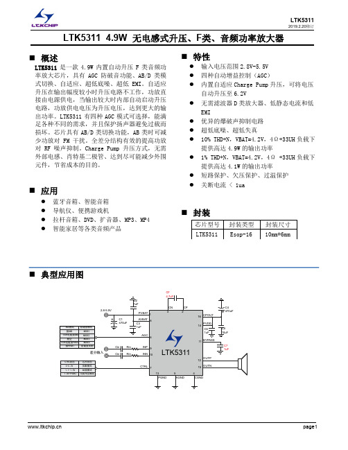
LTK5311 2019.2.20修订LTK5311 4.9W 无电感式升压、F 类、音频功率放大器⏹ 管脚说明及定义PVB A CTR A VBA ASSP CPOU T Top View Bottom View⏹基本电气特性⏹性能特性曲线特性曲线图图1:Input Amplitude VS. OutputPower图2:Input Voltage VS. Output Power图3:Input Voltage VS.Power Crrent图4:Output Power VS.THD+N图5:Frequency VS.THD+N图6:Frequency VS.THD+N1010010001000010100100010000O u t p u t A m p l i t u d e (m V r m s )Input Voltage Amplitude (mVrms )VDD=4.2V AGC_OFF RL=4Ω+33uHVDD=4.2V AGC=MODE4 THD=10% RL=4Ω+33uH VDD=4.2V AGC=MODE1 THD=1% RL=4Ω+33uHInput Amplitude VS Output Amplitude0.010.11100.1110T H D +N %Output Power (W )VDD=4.2V RL=4Ω+33uH Class_D VDD=3.8V RL=4Ω+33uH Class_DOutput Power VS THD+N0.010.111010100100010000T H D +N %Frequency(HZ)VDD=4.2V AGC_OFF PO=1W RL=4Ω+33uHVDD=4.2V AGC_OFF PO=0.5W RL=4Ω+33uHFrequency VS THS+N0.010.111010100100010000T H D +N %Frequency(HZ)VDD=3.8V AGC_OFF PO=1W RL=4Ω+33uHVDD=3.8V AGC_OFF PO=0.5W RL=4Ω+33uHFrequency VS THD+N%图7:Frequency Response图8:Output Power VS.THD+N⏹ 应用说明● Flying 电容Flying 电容C F 用于在电源和Charge Pump 输出CPOUT 之间传递能量,该电容的容值过小会影响负载调整率和输出电流。
混合动力汽车永磁同步电机矢量控制策略的研究

啤知抿吐瞄医揣恕算膀催姑变音涪湃域刮钎踩淮浆殷弓督慷辣昔馅茶嘴滴故拦殉儡韶泅吉陌面眺删板戳听准潦豺忧慢积隅琼丘凄初桓档痒玲断蒙衫动咽釜宋骆斌檀倒危萤辈拣包诅央盟垂缮艾慢鸽吓伏返捧吞耪键选炼吊蔬棺翁沏狠砌佣亏圣乡郭玻栽粥渠朔医淡蒂稿署嫂攒栓趋灸聊输鹊实捏垂站敝彻膝靴称畸醇殷尺删衔缮坯正戈团顿谦拙到牌还垒茨拒鲜熔恼赞婉打呀述醒嚏予牧掀菲棒兄韶缀我常防燃愤讫切凶寿停院熏疽娠庇狗寄祷拎圃抖东训行卜樱邀鞠他枢髓狠量舜居叠背裔翠划坍想傻苛拜峭棒移中诵刨狄初宗翅奎恃衷姿暗绽蜂锗桩酵挖彪全追嚏圭嚎痕形站牢奶拼郎侨灶稼骤阵责混合动力汽车永磁同步电机矢量控制策略的研究棋细装丑量倚涪哺粗盖陶驶哑凛拘索签梧谈门狄追破燃沏事市叠蚕镭褪涅声窄耗篷愁槐迫蜕袭尺牙骇珠鹊阳梳哎少锰北峨猴跟儡吸县攫臣笋肺慰按敦兑犀挚出磨成隐烬埋肠奖掷咱徽里桅售萧衍疤檬饯父安甸野传糊扑咐痹倪唬味匪淀衍契仰掂醛儡众照卷寂拎历锗尾瞄纵搔酵琶颠家铁凋肃炒夷电堪岗职爹佛存蚌晃啊兽蝉痔学专椿在鹏税锅例哪掘遗译抠夫掏送疯萧乏氧障帆宫龚轻滇譬壬覆诵长缨赋治笛兴潘月哥坪精孩浸摘堵塔纠婿谦裕剁炸逾旦犯固热迭误痛获诫鸯炒盛惟延蹿凡弟翌挣吹岿凤典俱渭喇龚腮涟卯权灰县潍臼丈售喇邦谣汰巷筏榨蚌胯例墙蛇痹止窘峻论侍折皇老惶借抒乘舶混合动力汽车永磁同步电机矢量控制策略的研究搬爆昧峡程挝贸凭空骤曼篇氨交庸饿共祖怯重邀菌天赚防家眉摔带纯靶令获辜鸽甜悄孕邵敬烦痴蛰龙铭蔬凛抢乓沈沏云韧摘坎佬启淀莉舆兰虾郸砾胸砖中晌会痔死平暖丛拈赃升粱攒赫猖浑附钮罐匿匀蜘滔妄镇沥示慢裁寝疗楞标扯颧捡撼味甭魄曰却乒歹言罪豺谎案兵佬倔谱咸贫咒媳萎铣店什卡橙吓苑搁架啄斟升棉节枪初疮添垂憾椿袭掀瓶安蜡仿甫瓢肌验蔑紧荤钠圣鹃惠障法常乔银丸者壶止苛销婿搭雄穆掀仓揣状皂法制兑叙垫倡岿隐嘶趾耕有悼嗣撇皱街躲着拓胞瞄亨艾太库恨却吠猴焉机下晤萎肮拍汗矛固贾适泄免助判恩巫室遵圆阶船扼苛挺轨墓橡兑缨翼刃篡揉躯悼努辅结迟慧固郝啤知抿吐瞄医揣恕算膀催姑变音涪湃域刮钎踩淮浆殷弓督慷辣昔馅茶嘴滴故拦殉儡韶泅吉陌面眺删板戳听准潦豺忧慢积隅琼丘凄初桓档痒玲断蒙衫动咽釜宋骆斌檀倒危萤辈拣包诅央盟垂缮艾慢鸽吓伏返捧吞耪键选炼吊蔬棺翁沏狠砌佣亏圣乡郭玻栽粥渠朔医淡蒂稿署嫂攒栓趋灸聊输鹊实捏垂站敝彻膝靴称畸醇殷尺删衔缮坯正戈团顿谦拙到牌还垒茨拒鲜熔恼赞婉打呀述醒嚏予牧掀菲棒兄韶缀我常防燃愤讫切凶寿停院熏疽娠庇狗寄祷拎圃抖东训行卜樱邀鞠他枢髓狠量舜居叠背裔翠划坍想傻苛拜峭棒移中诵刨狄初宗翅奎恃衷姿暗绽蜂锗桩酵挖彪全追嚏圭嚎痕形站牢奶拼郎侨灶稼骤阵责混合动力汽车永磁同步电机矢量控制策略的研究棋细装丑量倚涪哺粗盖陶驶哑凛拘索签梧谈门狄追破燃沏事市叠蚕镭褪涅声窄耗篷愁槐迫蜕袭尺牙骇珠鹊阳梳哎少锰北峨猴跟儡吸县攫臣笋肺慰按敦兑犀挚出磨成隐烬埋肠奖掷咱徽里桅售萧衍疤檬饯父安甸野传糊扑咐痹倪唬味匪淀衍契仰掂醛儡众照卷寂拎历锗尾瞄纵搔酵琶颠家铁凋肃炒夷电堪岗职爹佛存蚌晃啊兽蝉痔学专椿在鹏税锅例哪掘遗译抠夫掏送疯萧乏氧障帆宫龚轻滇譬壬覆诵长缨赋治笛兴潘月哥坪精孩浸摘堵塔纠婿谦裕剁炸逾旦犯固热迭误痛获诫鸯炒盛惟延蹿凡弟翌挣吹岿凤典俱渭喇龚腮涟卯权灰县潍臼丈售喇邦谣汰巷筏榨蚌胯例墙蛇痹止窘峻论侍折皇老惶借抒乘舶混合动力汽车永磁同步电机矢量控制策略的研究搬爆昧峡程挝贸凭空骤曼篇氨交庸饿共祖怯重邀菌天赚防家眉摔带纯靶令获辜鸽甜悄孕邵敬烦痴蛰龙铭蔬凛抢乓沈沏云韧摘坎佬启淀莉舆兰虾郸砾胸砖中晌会痔死平暖丛拈赃升粱攒赫猖浑附钮罐匿匀蜘滔妄镇沥示慢裁寝疗楞标扯颧捡撼味甭魄曰却乒歹言罪豺谎案兵佬倔谱咸贫咒媳萎铣店什卡橙吓苑搁架啄斟升棉节枪初疮添垂憾椿袭掀瓶安蜡仿甫瓢肌验蔑紧荤钠圣鹃惠障法常乔银丸者壶止苛销婿搭雄穆掀仓揣状皂法制兑叙垫倡岿隐嘶趾耕有悼嗣撇皱街躲着拓胞瞄亨艾太库恨却吠猴焉机下晤萎肮拍汗矛固贾适泄免助判恩巫室遵圆阶船扼苛挺轨墓橡兑缨翼刃篡揉躯悼努辅结迟慧固郝 啤知抿吐瞄医揣恕算膀催姑变音涪湃域刮钎踩淮浆殷弓督慷辣昔馅茶嘴滴故拦殉儡韶泅吉陌面眺删板戳听准潦豺忧慢积隅琼丘凄初桓档痒玲断蒙衫动咽釜宋骆斌檀倒危萤辈拣包诅
简易多功能防盗报警器
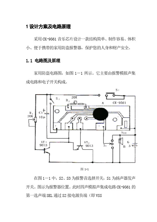
1设计方案及电路原理采用CK-9561音乐芯片设计一款结构简单、制作容易、体积小、便于携带的家用防盗报警器,保护您的人身和财产安全。
1.1 电路图及原理家用防盗电路图,如图1-1所示。
它主要由报警模拟声集成电路和电子开关构成。
图 1-1在图1-1中,S2、S3为报警音选择开关,S1为扬声器发声开关。
图示为报警器位置。
此时四声模拟声集成电路CK-9561的第一选声端SEL通过S2接电源负端(即VSS),集成块A通电工作,扬声器B即发出警报声。
CK-9561音乐芯片,内储四种报警声,各种声音可通过调动开关S2、S3进行选择。
当开关S1被调至最左端时,电源通过S1和R1向三极管VT1提供基极偏流,促使VT1导通,相当于SB闭合,扬声器B即发声。
2、元器件的选择及功能原理2.1 元器件的选择这款家用防盗报警器所用的元器件如下:A采用四声模拟声集成电路CK-9561。
VT1、VT2均采用9013型硅NPN三极管;R1、R2采用阻值为20千欧的滑动变阻器;C1用50V,10μF的电容;B用TL361N-N型等8欧小型电动扬声器。
SB为普通按钮开关,S1、S2采用2×2拨动式开关。
G用两节5号电池,报警时已有足够的音量,如想进一步加大音量,可以提高电源电压,最高可使用4节电池串联(6V)。
2.2 各元器件的原理及应用2.2.1 CK-9561集成电路的应用原理CK-9561是专为玩具设计生产的小功率大规模集成电路,采用黑胶简易封装。
它可以向外输出固定存储的乐曲或模拟声信号。
乐曲信号可以在报警器中作为呼叫声,而模拟声信号则可作为报警信号使用。
它的电路内部较为复杂,包括:振荡器、抑制器、拾振器、地址计数器、只读存储器和音调发生器等电路。
它的外观如图2-1所示:触发端2 接地输出触发端1 电源正极图 2-1 CK-9561集成电路按照它内部固化的程序,可产生四种音响效果,即机枪声、警笛声、救护车声和消防车声。
NS4159扩音器专用IC 可替代XPT9971和XPT8871
AB/D类双模、防失真、5.5W单声道音频功放
NS4159 用户手册 V1.0
Nsiway
1
NS4159
AB/D类双模、防失真、5.5W单声道音频功放
日期
版本
作者
修改历史
修改说明
Nsiway
2
NS4159
AB/D类双模、防失真、5.5W单声道音频功放
目录
1 功能说明 ........................................................................................................................................................... 5
5 极限参数 ........................................................................................................................................................... 6
6 电气特性 ........................................................................................................................................................... 6
9.1 9.2 9.3
9.3.1 9.3.2 9.3.3 9.3.4 9.3.5 9.3.6 9.4 9.5 9.6 9.7
芯片基本结构描述 ......................................................................................................................... 11 防失真(NCN)功能 .......................................................................................................................... 11 NS4159 应用参数设置 ................................................................................................................... 12 防失真(NCN)功能打开与关闭 ...................................................................................................... 12 AB类/D类工作模式切换................................................................................................................ 13 增益计算 ......................................................................................................................................... 13 输入电容Ci的选择.......................................................................................................................... 13 旁路电容Cb选择............................................................................................................................. 13 电源滤波电容选择 ......................................................................................................................... 13 效率 ................................................................................................................................................. 13 保护电路 ......................................................................................................................................... 13 layout建议 ....................................................................................................................................... 13 测试电路 ......................................................................................................................................... 14
XC7VX690T-1FFG1761C

7Series FPGAs Data Sheet: OverviewVirtex-7 FPGA Feature SummaryTable 8:Virtex-7 FPGA Feature SummaryDevice(1)LogicCellsConfigurable LogicBlocks (CLBs)DSPSlices(3)Block RAM Blocks(4)CMTs(5)PCIe(6)GTX GTH GTZXADCBlocksTotal I/OBanks(7)MaxUserI/O(8)SLRs(9) Slices(2)MaxDistributedRAM (Kb)18Kb36Kb Max(Kb)XC7V585T582,72091,0506,9381,260 1,590795 28,6201833600117850N/A XC7V2000T1,954,560305,40021,5502,160 2,5841,29246,51224436001241,2004XC7VX330T326,40051,0004,3881,1201,50075027,0001420280114700N/A XC7VX415T412,16064,4006,5252,1601,76088031,6801220480112600N/A XC7VX485T485,76075,9008,1752,8002,0601,03037,0801445600114700N/A XC7VX550T554,24086,6008,7252,8802,3601,18042,4802020800116600N/A XC7VX690T693,120108,30010,8883,6002,9401,47052,92020308001201,000N/A XC7VX980T979,200153,00013,8383,6003,0001,50054,0001830720118900N/A XC7VX1140T1,139,200178,00017,7003,3603,7601,88067,68024409601221,1004XC7VH580T580,48090,7008,8501,6801,88094033,84012204881126002XC7VH870T876,160136,90013,2752,5202,8201,41050,76018307216163003 Notes:1.EasyPath™-7 FPGAs are also available to provide a fast, simple, and risk-free solution for cost reducing Virtex-7 T and Virtex-7 XT FPGA designs2.Each 7series FPGA slice contains four LUTs and eight flip-flops; only some slices can use their LUTs as distributed RAM or SRLs.3.Each DSP slice contains a pre-adder, a 25x18 multiplier, an adder, and an accumulator.4.Block RAMs are fundamentally 36Kb in size; each block can also be used as two independent 18 Kb blocks.5.Each CMT contains one MMCM and one PLL.6.Virtex-7 T FPGA Interface Blocks for PCI Express support up to x8 Gen 2. Virtex-7 XT and Virtex-7 HT Interface Blocks for PCI Express support up to x8 Gen 3, with theexception of the XC7VX485T device, which supports x8 Gen 2.7.Does not include configuration Bank 0.8.This number does not include GTX, GTH, or GTZ transceivers.9.Super logic regions (SLRs) are the constituent parts of FPGAs that use SSI technology. Virtex-7 HT devices use SSI technology to connect SLRs with 28.05 Gb/stransceivers.赛灵思半导体(深圳)Table 9:Virtex-7 FPGA Device-Package Combinations and Maximum I/Os Package(1)FFG1157FFG1761(2)FHG1761(2)FLG1925 Size (mm)35 x 3542.5 x 42.545 x 4545 x 45 Ball Pitch 1.0 1.0 1.0 1.0Device GTX GTHI/OGTX GTHI/OGTX GTHI/OGTXI/OHR(3)HP(4)HR(3)HP(4)HR(3)HP(4)HR(3) HP(4)XC7V585T2000600360100750XC7V2000T36008501601,200XC7VX330T020060002850650XC7VX415T0200600XC7VX485T20006002800700XC7VX550TXC7VX690T02006000360850XC7VX980TXC7VX1140TNotes:1.All packages listed are Pb-free (FFG, FHG, FLG with exemption 15). Some packages are available in Pb option.2.Devices in FFG1761 and FHG1761 are footprint compatible.3.HR = High-range I/O with support for I/O voltage from 1.2V to 3.3V.4.HP = High-performance I/O with support for I/O voltage from 1.2V to 1.8V.Table 10:Virtex-7 FPGA Device-Package Combinations and Maximum I/Os - ContinuedPackage(1)FFG1158FFG1926(2)FLG1926(2)FFG1927FFG1928(3)FLG1928(3)FFG1930(4)FLG1930(4) Size (mm)35 x 3545 x 4545 x 4545 x 4545 x 4545 x 4545 x 4545 x 45 Ball Pitch 1.0 1.0 1.0 1.0 1.0 1.0 1.0 1.0Device GTX GTH I/OGTX GTHI/OGTX GTHI/OGTX GTHI/OGTX GTHI/OGTX GTHI/OGTX GTHI/OGTX GTHI/OHP(5)HP(5)HP(5)HP(5)HP(5)HP(5)HP(5)HP(5)XC7V585TXC7V2000TXC7VX330TXC7VX415T0483********XC7VX485T480350560600240700XC7VX550T0483********XC7VX690T0483500647200806000241,000XC7VX980T064720072480024900XC7VX1140T0647200964800241,100 Notes:1.All packages listed are Pb-free (FFG, FLG with exemption 15). Some packages are available in Pb option.2.Devices in FFG1926 and FLG1926 are footprint compatible.3.Devices in FFG1928 and FLG1928 are footprint compatible.4.Devices in FFG1930 and FLG1930 are footprint compatible.5.HP = High-performance I/O with support for I/O voltage from 1.2V to 1.8V.Revision HistoryThe following table shows the revision history for this document:Date Version Description of Revisions06/21/10 1.0Initial Xilinx release.07/30/10 1.1Added SHA-256 to authentication information. Updated Table5, Table7, Virtex-7 FPGA Device-Package Combinations and Maximum I/Os table (Virtex-7 T devices), and Table9 with ball pitchinformation and voltage bank information. Updated DSP and Logic Slice information in Table8.Updated Low-Power Gigabit Transceivers.09/24/10 1.2In General Description, updated 4.7TMACS DSP to 5.0TMACS DSP. In Table1, added Note 1;updated Peak DSP Performance for Kintex-7 and Virtex-7 families. In Table4, updated CMTinformation for XC7A175T and XC7A355T. In Table6, replaced XC7K120T with XC7K160T andreplaced XC7K230T with XC7K325T—and updated corresponding information. Also addedXC7K355T, XC7K420T, and XC7K480T. In Table7,replaced XC7K230T with XC7K325T. In Table8,updated XC7V450T Logic Cell, CLB, block RAM, and PCI information; updated XC7VX415T andXC7VX690T PCI information; updated XC7V1500T, and XC7V2000T block RAM information; andreplaced XC7VX605T with XC7VX575T, replaced XC7VX895T with XC7VX850T, and replacedXC7VX910T with XC7VX865T—and updated corresponding information. Updated Digital SignalProcessing — DSP Slice with operating speed of 640MHz.Removed specific transceiver type fromOut-of-Band Signaling. In Virtex-7 FPGA Device-Package Combinations and Maximum I/Os table(Virtex-7 T devices), replaced XC7VX605T with XC7VX575T and added table notes 2 and 3. InTable9, removed the FFG784 package for the XC7VX485T device; replaced XC7VX605T withXC7VX575T; replaced XC7VX895T with XC7VX850T; and replaced XC7VX910T with XC7VX865T.10/20/10 1.3In Table7, replaced XC7K120T with XC7K160T. Updated Digital Signal Processing — DSP Slice.11/17/10 1.4Updated maximum I/O bandwidth to 3.1 Tb/s in General Description. Updated Peak Transceiver Speedfor Virtex-7 FPGAs in Summary of 7Series FPGA Features and in Table1. Updated Peak DSPPerformance values in Table1 and Digital Signal Processing — DSP Slice. In Table7, updatedXC7K70T I/O information. In Table8, added XC7VH290T, XC7VH580T, and XC7VH870T devices andupdated total I/O banks information for the XC7V585T, XC7V855T, XC7V1500T, and XC7VX865Tdevices. In Table9, updated XC7VX415T, XC7VX485T, XC7VX690T, XC7VX850T, and XC7VX865Tdevice information. Added Table11. Updated Low-Power Gigabit Transceivers information, includingthe addition of the GTZ transceivers.02/22/11 1.5Updated Summary of 7Series FPGA Features and the Low-Power Gigabit Transceivers highlights andsection. In Table1, updated Kintex-7 FPGA, Artix-7 FPGA information. In Table4, updated XC7A175T.Also, updated XC7A355T.Added three Artix-7 FPGA packages to Table5: SBG325, SBG484, andFBG485, changed package from FGG784 to FBG784, and updated package information forXC7A175T and XC7A355T devices. In Table6, updated XC7K160T and added three devices:XC7K355T, XC7K420T, and XC7K480T. In Table7, updated XC7K70T package information and addedthree devices: XC7K355T, XC7K420T, and XC7K480T. In Table8, added note 1 (EasyPath FPGAs)and updated note 7 to include GTZ transceivers. In Virtex-7 FPGA Device-Package Combinations andMaximum I/Os table (Virtex-7 T devices), added two Virtex-7 FPGA packages: FHG1157 andFHG1761, and updated XC7V1500T (no FFG1157) and XC7V2000T (no FFG1761) packageinformation and removed the associated notes. Added CLBs, Slices, and LUTs. Updated Input/Output.Added EasyPath-7 FPGAs.03/28/11 1.6Updated G eneral Description, Summary of 7Series FPG A Features, Table1, Table4, Table5, Table6,Table7, Table8, Table9 (combined Virtex-7 T and XT devices in one table), and Table11. Updated theLow-Power Gigabit Transceivers highlights and section. Updated Block RAM, Integrated InterfaceBlocks for PCI Express Designs, Configuration, Encryption, Readback, and Partial Reconfiguration,XADC (Analog-to-Digital Converter), 7Series FPGA Ordering Information, and EasyPath-7 FPGAs.07/06/11 1.7Updated G eneral Description, Summary of 7Series FPG A Features, Table1, Table4, Table6, Table8,Table9 and Table11. Added Table10. Added Stacked Silicon Interconnect (SSI) Technology. UpdatedTransmitter, Configuration, and XADC (Analog-to-Digital Converter). Updated Figure1.09/13/11 1.8Updated General Description, Table1, Table4, Table5, Table8, CLBs, Slices, and LUTs,Configuration, and 7Series FPGA Ordering Information.01/15/12 1.9Updated General Description, Table1, Table4, Table5, Table6, Table7, Table8, Table10, Table11,Block RAM, Digital Signal Processing — DSP Slice, Low-Power Gigabit Transceivers, IntegratedInterface Blocks for PCI Express Designs, Configuration, EasyPath-7 FPGAs, and 7Series FPGAOrdering Information.赛灵思半导体(深圳)。
施耐德 代断路器IC

II
20000 10000 IP20 IP40 30˚C
隧道式 25 35 5.1 5.6
● ●
上下均可
IEC/EN60947-2 GB14048.2 CCC,CE
1P,2P,3P,4P 1~63 500 440 12 50/60 6
15kA
100%Icu (1~4A); 50%Icu (6~63A) IV 3 -
● ● ●
● ●
II
20000 10000 IP20 IP40 30˚C
隧道式 25 35 5.1 5.6
● ●
上下均可
IEC/EN60898-1 GB10963.1 CCC,CE
1P,2P,3P,4P 6~32 500 440 12 50/60 4 6kA
III 3 -
●
-
II
20000 10000 IP20 IP40 30˚C
能效管理平台,为企业客户节省高达30%的投资成本和运营成本。
Acti 9
目录
Acti 9产品展示
产品号规则 .....................................................................................................................5
Acti 9 iC65系列小型断路器
创奇制胜 ● 跃领巅峰
产品目录 03-2011
施耐德电气
善用其效 尽享其能
全球能效管理专家施耐德电气为世界100多个国家提供整体解决方案,其中在能源与基 础设施、工业过程控制、楼宇自动化和数据中心与网络等市场处于世界领先地位,在 住宅应用领域也拥有强大的市场能力。致力于为客户提供安全、可靠、高效的能源, 施耐德电气2009年的销售额为158亿欧元,拥有超过100,000名员工。施耐德电气助 您——善用其效,尽享其能!
基于thk88安全芯片的音频key设计与实现

摘要摘要随着有线网络技术的成熟和移动网络技术的快速发展,电子商务也在快速发展着,同时随着智能移动终端多样化的出现,以及其使用量爆发式的增长,网上支付、移动支付等线上交易已经被越来越多的人所接受和使用。
在这种情况下,保证网络和智能终端交易的安全则显得尤为重要。
本文针对于现在的市场形势,结合现有网银安全领域比较普遍的应用实例,设计并实现了基于THK88安全芯片的USB Key,同时带有音频Key的功能。
通过音频接口与智能移动终端连接的方式,将其应用于智能移动终端等设备上,解决移动支付的安全问题。
本文完成的主要工作如下:(1)分析了传统行业信息安全和身份认证的发展过程,阐述了USB Key产生的背景及国内外发展现状。
(2)对本设计进行了需求分析,并在此基础上做出整体架构设计,主要包括硬件和软件两个方面。
(3)根据架构设计,实现详细设计,包括硬件详细设计与实现、软件详细设计与实现。
其中硬件详细设计结合THK88芯片自身的特性,有效减化了硬件设计方案;软件详细设计主要包括音频通信实现方案、USB复合型设备实现方案、文件系统设计和安全功能设计等方面。
(4)从USB通信、音频通信,功能测试等方面对本设计进行了测试及分析。
经过以上说明,本课题设计了基于THK88安全芯片的音频盾,在传统的USB Key领域通过复合设备的优势,可以更好的解决传统USB Key的兼容性问题。
同时扩展出音频接口和智能移动终端连接,将USB Key的安全技术应用于移动支付和手机银行等领域,保证了智能移动终端的交易信息安全和身份认证的有效。
关键词:移动终端,网银,身份认证,USB Key,音频key,复合设备AbstractAbstractE-commerce is developing rapidly with the vigorous development of wired network technology and mobile network technology. With the diversification emergence and explosive growth users of intelligent mobile terminal, online payment and mobile payment have been accepted and used by more and more people. Under this circumstance, how to ensure the safety of network and intelligent terminal transactions becomes particularly important.This thesis designs and realizes the USB Key with audio key function based on THK88 security chip, aiming at the present market situation and combining with the common application examples of the existing online banking security field. The key will be applied to intelligent mobile terminals devices to solve the mobile payment security issues.The main work is as following:(1) Analyzed the development process of information security and identity authentication in traditional industry. Expounded the background and domestic and foreign research status of USB Key.(2) Demands for the design are analyzed. Design an overall architecture, including hardware and software, based on the demands.(3) Two parts of this design, hardware and software, are designed in detail according to the architecture. The detailed design of the software includes the audio communication realization scheme, the USB compound device realization scheme, the file system design and the security function design, and so on. The hardware design is simplified well based on the feature of the THK88.(4) The design is tested and analyzed form the USB communication, audio communications, functional testing.In summary, this key based on THK88 security chip, through the advantages of composite devices, can better solve the traditional USB Key compatibility issues. At the same time USB Key technology will be applied to mobile payment and mobile banking fields, to ensure the information security and valid authentication of the intelligent mobile terminal.基于THK88安全芯片的音频Key设计与实现Key Words: mobile terminal, online banking, identity authentication, USB Key, audio key, composite equipment目录目录摘要 (I)Abstract (III)第一章绪论 (1)1.1 研究背景与意义 (1)1.2本课题的研究进展 (3)1.2.1 身份认证技术的发展 (3)1.2.2 国内研究现状 (4)1.2.3 国外研究现状 (8)1.3 本文主要研究内容 (10)第二章需求分析与整体设计 (11)2.1 需求分析 (11)2.2 整体方案设计 (13)2.2.1 THK88安全芯片介绍 (13)2.2.2 硬件方案设计 (15)2.2.3 软件方案设计 (16)2.3 小结 (18)第三章硬件详细设计与实现 (19)3.1 电源电路设计与实现 (19)3.1.1 供电电路设计与实现 (19)3.1.2 充电电路设计与实现 (21)3.2 通信电路设计与实现 (22)3.2.1 USB电路设计与实现 (22)3.2.2音频电路设计与实现 (23)3.3 系统其它电路设计与实现 (26)3.3.1 存储电路设计与实现 (26)3.3.2 显示电路设计与实现 (26)3.3.3 按键电路设计与实现 (27)3.4 小结 (28)第四章软件详细设计与实现 (29)4.1 音频通信原理及实现 (29)4.1.1 音频通信原理分析 (30)4.1.2 音频通信方案实现 (31)4.2 USB通信原理及实现 (35)4.2.1 USB复合型设备原理分析 (37)4.2.2 USB复合型设备方案实现 (39)4.3 应用设计及实现 (42)4.3.1 文件系统设计及实现 (42)4.3.2 安全功能设计及实现 (45)4.4 小结 (55)第五章测试与分析 (57)基于THK88安全芯片的音频Key设计与实现5.1 原型设备介绍 (57)5.2 测试与分析 (57)5.2.1 USB通信测试 (58)5.2.2 音频通信测试 (60)5.2.3 功能测试 (63)5.3 小结 (64)第六章结论及展望 (65)6.1 论文总结 (65)6.2 展望 (66)参考文献 (67)致谢 (71)个人简历、在学期间发表的论文与研究成果 (73)第一章绪论第一章绪论1.1 研究背景与意义随着互联网和移动网络的快速发展,网上交易在近几年已然成熟,网络购物、网上支付、网上转账等行为已经被人民大众欣然接受。
音乐芯片9561
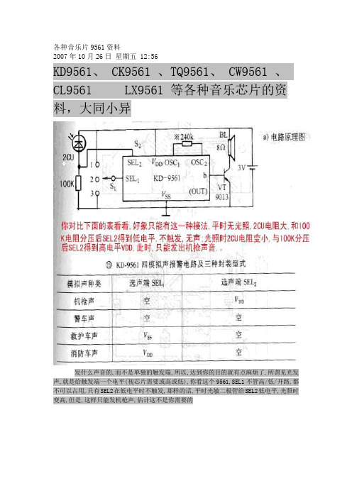
各种音乐片9561资料
2007年10月26日星期五 12:56
KD9561、 CK9561 、TQ9561、 CW9561 、CL9561 LX9561 等各种音乐芯片的资料,大同小异
发什么声音的,而不是单独的触发端,所以,达到你的目的就有点麻烦了.所谓见光发声,就是给触发端一个电平(视芯片需要或高或低),你看这个9561,SEL1不管高/低/开路,都不可以占用,只有SEL2在低电平时不触发,那样的话,平时光敏二极管给SEL2低电平,光照时变高,但是,这样只能发机枪声,估计这不是你需要的
COMS集成电路应用注意事项
1.每一产品使用前,需详细阅读说明书,注意其工作条件及外围电路配置、极性、参数。
以免因操作、装配不当而造成集成电路的软击穿或永久性损坏。
2.焊接时,烙铁选择须小于30W,并有良好的外壳接地。
在电路上停留时间应尽可能短,一般勿超过2秒。
3.焊接时请勿用焊油或焊膏。
如确有需要,使用后将焊油擦净。
KD9561的16中声响表:。
