PD703002GC-25-xxx-8EU中文资料
EPA8270D中文
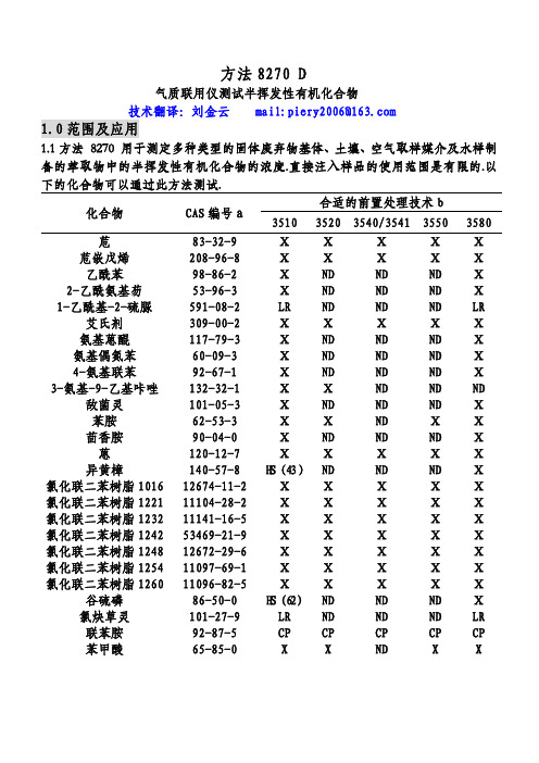
方法8270 D气质联用仪测试半挥发性有机化合物技术翻译:刘金云 mail:piery2006@1.0范围及应用1.1方法 8270 用于测定多种类型的固体废弃物基体、土壤、空气取样媒介及水样制备的萃取物中的半挥发性有机化合物的浓度.直接注入样品的使用范围是有限的.以下的化合物可以通过此方法测试.合适的前置处理技术b 化合物 CAS编号a3510 35203540/3541 35503580 苊 83-32-9 Ⅹ Ⅹ Ⅹ Ⅹ Ⅹ 苊嵌戊烯 208-96-8 Ⅹ Ⅹ Ⅹ Ⅹ Ⅹ乙酰苯 98-86-2 Ⅹ ND ND ND Ⅹ 2-乙酰氨基芴 53-96-3 Ⅹ ND ND ND Ⅹ 1-乙酰基-2-硫脲 591-08-2 LR ND ND ND LR 艾氏剂 309-00-2 Ⅹ Ⅹ Ⅹ Ⅹ Ⅹ 氨基蒽醌 117-79-3 Ⅹ ND ND ND Ⅹ 氨基偶氮苯 60-09-3 Ⅹ ND ND ND Ⅹ 4-氨基联苯 92-67-1 Ⅹ ND ND ND Ⅹ 3-氨基-9-乙基咔唑 132-32-1 Ⅹ Ⅹ ND ND ND 敌菌灵 101-05-3 Ⅹ ND ND ND Ⅹ苯胺 62-53-3 Ⅹ Ⅹ ND Ⅹ Ⅹ茴香胺 90-04-0 Ⅹ ND ND ND Ⅹ 蒽 120-12-7 Ⅹ Ⅹ Ⅹ Ⅹ Ⅹ 异黄樟 140-57-8 H S(43)ND ND ND Ⅹ 氯化联二苯树脂101612674-11-2 Ⅹ Ⅹ Ⅹ Ⅹ Ⅹ 氯化联二苯树脂122111104-28-2 Ⅹ Ⅹ Ⅹ Ⅹ Ⅹ 氯化联二苯树脂123211141-16-5 Ⅹ Ⅹ Ⅹ Ⅹ Ⅹ 氯化联二苯树脂124253469-21-9 Ⅹ Ⅹ Ⅹ Ⅹ Ⅹ 氯化联二苯树脂124812672-29-6 Ⅹ Ⅹ Ⅹ Ⅹ Ⅹ 氯化联二苯树脂125411097-69-1 Ⅹ Ⅹ Ⅹ Ⅹ Ⅹ 氯化联二苯树脂126011096-82-5 Ⅹ Ⅹ Ⅹ Ⅹ Ⅹ 谷硫磷 86-50-0 H S(62)ND ND ND Ⅹ 氯炔草灵 101-27-9 LR ND ND ND LR联苯胺 92-87-5 CP CP CP CP CP苯甲酸 65-85-0 X X ND X X合适的前置处理技术 b 化合物 CAS编号a3510 35203540/3541 35503580 苯并蒽 56-55-3 Ⅹ Ⅹ Ⅹ Ⅹ Ⅹ 苯并(b)荧蒽 205-99-2 Ⅹ Ⅹ Ⅹ Ⅹ Ⅹ 苯并(k)荧蒽 207-08-9 Ⅹ Ⅹ Ⅹ Ⅹ Ⅹ 苯并(g,h,i)茈 191-24-2 Ⅹ Ⅹ Ⅹ Ⅹ Ⅹ 苯并(a)芘 50-32-8 Ⅹ Ⅹ Ⅹ Ⅹ Ⅹ p-苯醌 106-51-4 OE ND ND ND X苯甲醇 100-51-6 Ⅹ Ⅹ ND Ⅹ Ⅹ α-六氯化苯 319-84-6 Ⅹ Ⅹ Ⅹ Ⅹ Ⅹ β-六氯化苯 319-85-7 Ⅹ Ⅹ Ⅹ Ⅹ Ⅹ δ-六氯化苯 319-86-8 Ⅹ Ⅹ Ⅹ Ⅹ Ⅹ γ-六氯化苯(林旦)58-89-9 Ⅹ Ⅹ Ⅹ Ⅹ Ⅹ 双(2-氯乙氧基)甲烷111-91-1 Ⅹ Ⅹ Ⅹ Ⅹ Ⅹ 双(2-氯乙基)醚 111-44-4 Ⅹ Ⅹ Ⅹ Ⅹ Ⅹ 双(2-氯异丙基)醚108-60-1 Ⅹ Ⅹ Ⅹ Ⅹ Ⅹ 双(2-氯乙基己基)邻苯二甲酸酯117-81-7 Ⅹ Ⅹ Ⅹ Ⅹ Ⅹ 4-溴苯基苯醚 101-55-3 Ⅹ Ⅹ Ⅹ Ⅹ Ⅹ 溴苯腈 1689-84-5 Ⅹ ND ND ND Ⅹ 邻苯二甲酸丁基·苄基酯85-68-7 Ⅹ Ⅹ Ⅹ Ⅹ Ⅹ 敌菌丹 2425-06-1 H S(55)ND ND ND Ⅹ克菌丹 133-06-2 H S(40)ND ND ND Ⅹ甲萘威 63-25-2 Ⅹ ND ND ND Ⅹ呋喃丹 1563-66-2 Ⅹ ND ND ND Ⅹ二硫磷 786-19-6 Ⅹ ND ND ND Ⅹ 氯丹(NOS) 57-74-9 Ⅹ Ⅹ Ⅹ Ⅹ Ⅹ 毒虫威 470-90-6 Ⅹ ND ND ND Ⅹ 4-氯苯胺 106-47-8 Ⅹ ND ND ND Ⅹ 乙酯杀螨醇 510-15-6 Ⅹ ND ND ND Ⅹ 对氯邻氨基甲苯 95-79-4 Ⅹ ND ND ND Ⅹ 4-氯-3-甲苯酚 59-50-7 Ⅹ Ⅹ Ⅹ Ⅹ Ⅹ 3-(氯甲苯)吡啶盐6959-48-4 Ⅹ ND ND ND Ⅹ 酸盐1-氯代萘 90-13-1 Ⅹ Ⅹ Ⅹ Ⅹ Ⅹ 2-氯代萘 91-58-7 Ⅹ Ⅹ Ⅹ Ⅹ Ⅹ 2-氯苯酚 95-57-8 Ⅹ Ⅹ Ⅹ Ⅹ Ⅹ 4-氯-1,2-苯二胺 95-83-0 Ⅹ Ⅹ ND ND ND 4-氯-1,3-苯二胺 5131-60-2 Ⅹ Ⅹ ND ND ND 4-氯苯基苯醚 7005-72-3 Ⅹ Ⅹ Ⅹ Ⅹ Ⅹ合适的前置处理技术 b 化合物 CAS编号a3510 35203540/3541 35503580 1,2-苯并菲 218-01-9 Ⅹ Ⅹ Ⅹ Ⅹ Ⅹ 香豆磷 56-72-4 Ⅹ ND ND ND Ⅹ 甲酚定 120-71-8 Ⅹ ND ND ND Ⅹ 丁烯磷 7700-17-6 Ⅹ ND ND ND Ⅹ 2-环己烯-4,6-二硝基-苯酚131-89-5 Ⅹ ND ND ND LR 4,4-DDD 72-54-8 Ⅹ Ⅹ Ⅹ Ⅹ Ⅹ 4,4-DDE 72-55-9 Ⅹ Ⅹ Ⅹ Ⅹ Ⅹ 4,4-DDT 50-29-3 Ⅹ Ⅹ Ⅹ Ⅹ X O-异内吸磷 298-03-3 H S(68)ND ND ND Ⅹ S-异内吸磷 126-75-0 Ⅹ ND ND ND Ⅹ 燕麦敌(顺式或反式)2303-16-4 Ⅹ ND ND ND Ⅹ 2,4-二氨基甲苯 95-80-7 D C,0E(42)ND ND ND Ⅹ 二苯并(a,j)吖啶 224-42-0 ⅩND ND NDⅩ二苯并(a,h)蒽 53-70-3 ⅩⅩⅩⅩⅩ二苯并呋喃 132-64-9 ⅩⅩNDⅩⅩ二苯并(a,e)芘 192-65-4 ND ND ND NDⅩ1,2-溴-3-氯丙烷 96-12-8 ⅩⅩND ND ND 苯二甲酸-n-二丁酯 84-74-2 ⅩⅩⅩⅩⅩ二氯萘醌 117-80-6 OE ND ND NDⅩ1,2-二氯代苯 95-50-1 ⅩⅩⅩⅩⅩ1,3-二氯代苯 541-73-1 ⅩⅩⅩⅩⅩ1,4-二氯代苯 106-46-7 ⅩⅩⅩⅩⅩ3,3-二氯联苯胺 91-94-1 ⅩⅩⅩⅩⅩ2,4-二氯苯酚 120-83-2 ⅩⅩⅩⅩⅩ2,6-二氯苯酚 87-65-0 ⅩND ND NDⅩ敌敌畏 62-73-7 ⅩND ND NDⅩ百治磷 141-66-2 ⅩND ND NDⅩ狄氏剂 60-57-1 ⅩⅩⅩⅩⅩ酞酸二乙酯 84-66-2 ⅩⅩⅩⅩⅩ乙烯雌酚 56-53-1 AW,ND ND NDⅩ0S(67)硫酸二乙酯 64-67-5 LR ND ND ND LR 乐果 60-51-5 H E,ND ND NDⅩH S(31)3,3`-二甲氨基联苯氨 119-90-4 ⅩND ND ND LR 二甲氨基偶氮苯 60-11-7 ⅩND ND ND X 7,12甲基苯并(a)蒽 57-97-6 C P(45)ND ND ND CP合适的前置处理技术b 化合物 CAS编号a351035203540/3541 35503580 3,3`-二甲基联苯胺 119-93-7 Ⅹ ND ND ND Ⅹ α,α-二甲基苯乙胺 122-09-8 ND ND ND ND Ⅹ 2,4-二甲苯酚 105-67-9 Ⅹ Ⅹ Ⅹ Ⅹ Ⅹ 苯二甲酸二甲酯 131-11-3 Ⅹ Ⅹ Ⅹ Ⅹ Ⅹ 1,2-二硝基苯 528-29-0 Ⅹ ND ND ND X 1,3-二硝基苯 99-65-0 Ⅹ ND ND ND Ⅹ 1,4二硝基苯 100-25-4 H E(14)ND ND ND Ⅹ 4,6-二硝基-2-甲酚 534-52-1 Ⅹ Ⅹ Ⅹ Ⅹ Ⅹ 2,4-二硝基苯酚 51-28-5 Ⅹ Ⅹ Ⅹ Ⅹ Ⅹ 2,4-二硝基甲苯 121-14-2 Ⅹ Ⅹ Ⅹ Ⅹ Ⅹ 2,6二硝基甲苯 606-20-2 Ⅹ Ⅹ Ⅹ Ⅹ Ⅹ 敌螨普 39300-45-3 CP,HS ND ND ND CP(28)二硝丁酚 88-85-7 Ⅹ ND ND ND Ⅹ 二苯胺 122-39-4 Ⅹ Ⅹ X Ⅹ Ⅹ 苯妥英 57-41-0 X ND ND ND Ⅹ 1,2-二苯肼 122-66-7 Ⅹ Ⅹ Ⅹ Ⅹ Ⅹ 磷酸-n-二辛酯 117-84-0 Ⅹ Ⅹ Ⅹ Ⅹ Ⅹ 乙拌磷 298-04-4 X ND ND ND Ⅹ 硫丹Ⅰ 959-98-8 Ⅹ Ⅹ Ⅹ Ⅹ Ⅹ 硫丹Ⅱ 33213-65-9 Ⅹ Ⅹ Ⅹ Ⅹ Ⅹ 硫酸硫丹 1031-07-8 Ⅹ Ⅹ Ⅹ Ⅹ Ⅹ 异狄氏剂 72-20-8 Ⅹ Ⅹ Ⅹ Ⅹ Ⅹ 异狄氏剂醛 7421-93-4 Ⅹ Ⅹ Ⅹ Ⅹ Ⅹ 异狄氏剂酮 53494-70-5 Ⅹ X ND X Ⅹ 苯硫磷 2104-64-5 Ⅹ ND ND ND Ⅹ 乙硫磷 563-12-2 Ⅹ ND ND ND Ⅹ 氨基甲酸乙酯 51-79-6 D C(28)ND ND ND Ⅹ 乙基甲磺酸 62-50-0 Ⅹ ND ND ND Ⅹ 氨磺磷 52-85-7 Ⅹ ND ND ND Ⅹ 丰索磷 115-90-2 Ⅹ ND ND ND Ⅹ 倍硫磷 55-38-9 Ⅹ ND ND ND Ⅹ 氯氟灵 33245-39-5 Ⅹ ND ND ND Ⅹ荧蒽 206-44-0 Ⅹ Ⅹ Ⅹ Ⅹ Ⅹ芴 86-73-7 Ⅹ Ⅹ Ⅹ Ⅹ Ⅹ 2-氟(代)联苯 321-60-8 Ⅹ Ⅹ Ⅹ Ⅹ Ⅹ 2-氟(代)苯酚 367-12-4 Ⅹ Ⅹ Ⅹ Ⅹ Ⅹ合适的前置处理技术b 化合物 CAS编号a351035203540/3541 35503580 七氯化茚 76-44-8 X X X X X 七氯环氧化物 1024-57-3 X X X X X 六氯化苯 118-74-1 X X X X X 六氯丁二烯 87-68-3 X X X X X 六氯环戊二烯 77-47-4 X X X X X 六氯乙烷 67-72-1 X X X X X六氯酚 70-30-4 A W,ND ND ND CPC P(62)六氯丙烯 1888-71-7 X ND ND ND X 六甲基磷酸三酰胺 680-31-9 X ND ND ND X 对苯二酚 123-31-9 ND ND ND ND X 茚并(1,2,3-cd)芘 193-39-5 X X X X X 异艾氏剂 465-73-6 X ND ND ND X 异佛尔酮 78-59-1 X X X X X 异黄樟素 120-58-1 D C(46)ND ND ND X十氯酮 143-50-0 X ND ND ND X溴苯磷 21609-90-5 X ND ND ND X 马拉硫磷 121-75-5 HS(5)ND ND ND X 顺丁烯二酸酐 108-31-6 HE ND ND ND X 炔雌醇甲醚 72-33-3 X ND ND ND X 噻吩甲吡胺 91-80-5 X ND ND ND X 甲氧氯 72-43-5 X ND ND ND X 甲基胆蒽 56-49-5 X ND ND ND X 4,4`-亚甲基双 101-14-4 O E,O S ND ND ND LR (-2氯苯胺) (0)4,4`-亚甲基双 101-61-1 X X ND ND ND (N,N-二甲基-苯胺)甲基甲磺酸 66-27-3 X ND ND ND X 2-甲基萘 91-57-6 X X ND X X 甲基对硫磷 298-00-0 X ND ND ND X 2-甲苯酚 95-48-7 X ND ND ND X 3-甲苯酚 108-39-4 X ND ND ND X 4-甲苯酚 106-44-5 X ND ND ND X速灭磷 7786-34-7 X ND ND ND X兹克威 315-18-4 H E,H S ND ND ND X(68)灭蚁灵 2385-85-5 X ND ND ND X久效磷 6923-22-4 HE ND ND ND X合适的前置处理技术b 化合物 CAS编号a351035203540/3541 35503580 二溴磷 300-76-5 Ⅹ ND ND ND Ⅹ 萘 91-20-3 Ⅹ Ⅹ Ⅹ Ⅹ Ⅹ萘醌 130-15-4 Ⅹ ND ND ND Ⅹ1-萘胺 134-32-7 O S(44)ND ND ND Ⅹ2-萘胺 91-59-8 Ⅹ ND ND ND Ⅹ烟碱 54-11-5 D E(67)ND ND ND X 5-硝基苊 602-87-9 Ⅹ ND ND ND Ⅹ 2-硝基苯胺 88-74-4 Ⅹ Ⅹ ND Ⅹ Ⅹ 3-硝基苯胺 99-09-2 Ⅹ Ⅹ ND Ⅹ Ⅹ 4-硝基苯胺 100-01-6 Ⅹ Ⅹ ND Ⅹ Ⅹ 2-甲氧基-5-硝基苯胺 99-59-2 Ⅹ ND ND ND Ⅹ 硝基苯 98-95-3 Ⅹ Ⅹ Ⅹ Ⅹ Ⅹ 4-硝基联苯 92-93-3 Ⅹ ND ND ND Ⅹ 除草醚 1836-75-5 Ⅹ ND ND ND Ⅹ 2-硝基苯酚 88-75-5 Ⅹ Ⅹ Ⅹ Ⅹ Ⅹ 4-硝基苯酚 100-02-7 Ⅹ Ⅹ Ⅹ Ⅹ Ⅹ 5-硝基-2-甲苯胺 99-55-8 Ⅹ X ND ND Ⅹ 硝基硅啉-1-氧化物 56-57-5 Ⅹ ND ND ND Ⅹ N-亚硝基二丁胺 924-16-3 X ND ND ND Ⅹ N-亚硝基二乙胺 55-18-5 X ND ND ND Ⅹ N-亚硝基二甲胺 62-75-9 Ⅹ X X X Ⅹ N-亚硝基甲基乙胺 10595-95-6 Ⅹ ND ND ND Ⅹ N-亚硝基二苯胺 86-30-6 Ⅹ X X X Ⅹ N-亚硝基二丙胺 621-64-7 Ⅹ Ⅹ Ⅹ Ⅹ Ⅹ 亚硝基吗啉 59-89-2 ND ND ND ND Ⅹ N-亚硝基呱啶 100-75-4 Ⅹ ND ND ND Ⅹ 亚硝基吡咯烷 930-55-2 Ⅹ ND ND ND Ⅹ 八甲基焦磷酰胺 152-16-9 LR ND ND ND LR 4,4`-羟基二苯胺 101-80-4 Ⅹ ND ND ND Ⅹ 对硫磷 56-38-2 Ⅹ X ND ND Ⅹ五氯苯 608-93-5 X ND ND ND X 五氯硝基苯 82-68-8 Ⅹ ND ND ND Ⅹ 五氯苯酚 87-86-5 Ⅹ Ⅹ Ⅹ Ⅹ Ⅹ 非那西丁 62-44-2 Ⅹ ND ND NDⅩ 菲 85-01-8 Ⅹ Ⅹ X X X 菲巴比妥 50-06-6 Ⅹ ND ND ND Ⅹ 苯酚 108-95-2 D C(28)Ⅹ Ⅹ Ⅹ Ⅹ合适的前置处理技术b 化合物 CAS编号a3510 35203540/3541 35503580 1,4-苯二胺 106-50-3 Ⅹ ND ND ND Ⅹ 甲拌磷 298-02-2 Ⅹ Ⅹ Ⅹ Ⅹ Ⅹ 伏杀硫磷 2310-17-0 HS(65)ND ND ND Ⅹ 亚胺硫磷 732-11-6 HS(15)ND ND ND Ⅹ 磷胺 13171-21-6 H E(63)ND ND ND Ⅹ酞酐 85-44-9 C P,H E(1)ND ND ND CP 2-皮考啉(2-甲基吡啶)109-06-8 Ⅹ X ND ND ND 胡椒基亚砜 120-62-7 Ⅹ ND ND ND Ⅹ 拿草特 23950-58-5 Ⅹ ND ND ND Ⅹ 丙硫氧密啶 51-52-5 LR ND ND ND LR 芘 129-00-0 Ⅹ X X X Ⅹ 间苯二酚 108-46-3 DC,OE ND ND ND Ⅹ(10)Ⅹ 黄樟素 94-59-7 Ⅹ ND ND ND Ⅹ 番木鳖碱 57-24-9 AW,0S ND ND ND Ⅹ(55)菜草特 95-06-7 Ⅹ ND ND ND Ⅹ叔丁磷 13071-79-9 Ⅹ ND ND ND Ⅹ 1,2,4,5-四氯苯 95-94-3 X ND ND ND Ⅹ 2,3,4,6-四氯苯酚 58-90-2 X ND ND ND Ⅹ 杀虫畏 961-11-5 Ⅹ ND ND ND Ⅹ 四乙基二硫代焦磷酸3689-24-5 Ⅹ X ND ND ND 焦磷酸四乙酸酯 107-49-3 Ⅹ ND ND ND Ⅹ 硫磷嗪 297-97-2 Ⅹ ND ND ND Ⅹ 苯硫酚(硫酚) 108-98-5 X ND ND ND Ⅹ 甲苯二异氰酸酯 584-84-9 HE(6)ND ND ND Ⅹ 邻甲苯胺 95-53-4 Ⅹ ND ND ND Ⅹ毒杀芬 8001-35-2 X X X X X 1,2,3-三氯苯 120-82-1 Ⅹ X X X Ⅹ 2,4,5-三氯苯酚 95-95-4 Ⅹ X ND X Ⅹ 2,4,6-三氯苯酚 88-06-2 X X X X X 氟乐灵 1582-09-8 Ⅹ ND ND ND Ⅹ 2,4,5-三甲基苯胺 137-17-7 Ⅹ ND ND ND Ⅹ 磷酸三甲酯 512-56-1 H E(60)ND ND NDⅩ 1,3,5-三硝基苯 99-35-4 Ⅹ ND ND ND X 磷酸三(2,3-二溴丙基酯)126-72-7 Ⅹ ND ND ND LR合适的前置处理技术b 化合物 CAS编号a351035203540/3541 35503580 磷酸邻三甲苯酯 78-32-0 Ⅹ ND ND ND Ⅹ O,O,O-三乙基代磷酸酯126-68-1 Ⅹ ND ND ND Ⅹ a: CAS-化学文摘服务处.b: 其它可以接受的前置处理方法参见第1.2节.分析物目录要点:AW=在萃取和储存时,吸附到玻璃器皿内壁上.CP=不可重复的色谱性能DC=不理想的分布系数(括号中的数字为回收率百分数)HE=萃取时的水解作用在酸性或碱性条件的催化下加快(括号中的数字为回收率百分数).HS=储存时的水解作用(括号中的数字为稳定性百分率)LR=较低的回应ND=没有测试到OE=萃取时,在碱性条件的催化作用下氧化作用加快(括号中的数字为回收率百分数).OS=储存时被氧化(括号中的数字为稳定性百分率).X=通过此种技术回收率大于70%.1.2除了在以上的分析物目录中列出的样品制备方法外,方法3535描述的是一个固相萃取程序,可应用于从TCLP浸出液中(表16与表17中包含性能数据)提取半挥发性物质.方法3542描述的是气体中的半挥发性有机化合物的样品制备程序,气体是通过方法0010(表11中含有代用物的性能数据)取样的.方法3545描述的是利用溶剂从固体中自动萃取半挥发性物质的装置(表12包含有性能数据).方法3561描述的是从固体中萃取多环芳香烃类(PAHs)的超临界流体装置(见表格13,14,15中的性能数据). 1.3对于能溶解于二氯甲烷的中性、酸性和碱性有机化合物,且它们能够被洗脱,无需衍生化便可从气相色谱熔融二氧化硅毛细管柱(柱上涂有少量的极性硅酮)显现尖锐的峰,大多数这样的有机化合物可用方法8270来定量测试.这些化合物包括:多环芳香烃类(PAHs)、氯化烃类、农药、邻苯二甲酸酯类、有机磷酸酯类、亚硝胺类、卤代醚类、醛类、醚类、酮类、苯胺类、吡啶类、喹啉类、芳香族硝基化合物、酚类(包括硝基酚类)。
CNY70中文资料
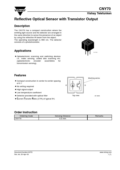
Dimensions of CNY70 in mm95 11345www.vishay.Document Number 83751Ozone Depleting Substances Policy StatementIt is the policy of Vishay Semiconductor GmbH to1.Meet all present and future national and international statutory requirements.2.Regularly and continuously improve the performance of our products, processes, distribution and operatingsystems with respect to their impact on the health and safety of our employees and the public, as well as their impact on the environment.It is particular concern to control or eliminate releases of those substances into the atmosphere which are known as ozone depleting substances (ODSs).The Montreal Protocol (1987) and its London Amendments (1990) intend to severely restrict the use of ODSs and forbid their use within the next ten years. Various national and international initiatives are pressing for an earlier ban on these substances.Vishay Semiconductor GmbH has been able to use its policy of continuous improvements to eliminate the use of ODSs listed in the following documents.1.Annex A, B and list of transitional substances of the Montreal Protocol and the London Amendments respectively2.Class I and II ozone depleting substances in the Clean Air Act Amendments of 1990 by the EnvironmentalProtection Agency (EPA) in the USA3.Council Decision 88/540/EEC and 91/690/EEC Annex A, B and C (transitional substances) respectively. Vishay Semiconductor GmbH can certify that our semiconductors are not manufactured with ozone depleting substances and do not contain such substances.We reserve the right to make changes to improve technical design and may do so without further notice. Parameters can vary in different applications. All operating parameters must be validated for each customer application by the customer. Should the buyer use Vishay Telefunken products for any unintended or unauthorized application, the buyer shall indemnify Vishay Telefunken against all claims, costs, damages, and expenses, arising out of, directly or indirectly, any claim of personal damage, injury or death associated with such unintended or unauthorized use.Vishay Semiconductor GmbH, P.O.B. 3535, D-74025 Heilbronn, GermanyTelephone: 49 (0)7131 67 2831, Fax number: 49 (0)7131 67 2423Document Number 83751。
8704N操作说明
2.4G 150M大功率室外CPE/APSL-8704N用户手册版本号:V2版权声明版权所有©2011深圳市天浩科技有限公司,保留所有权利。
文中提及到的其它商标或商品名称均是他们所属公司的商标或注册商标。
本产品的所有部分,包括配件和软件,其版权属深圳市天浩科技有限公司所有,在未经过深圳市天浩科技有限公司许可的情况下,不得任意拷贝、抄袭、仿制或翻译成其它语言。
本手册中的所有图片和产品规格参数仅供参考,随着软件或硬件的升级会略有差异,如有变更,恕不另行通知,如需了解更多产品信息,请浏览我们的网站:版权所有,不得翻印目录第一章:产品概述 (4)1.1产品简介 (4)1.2产品特性 (4)1.3产品应用 (5)1.4物品清单 (5)第二章:硬件描述 (6)2.1面板布置 (6)2.1.1前面板 (6)2.1.2后面板 (6)2.2复位 (7)2.3系统要求 (7)2.4. 安装环境 (8)第三章:连接宽带路由器 (9)1、登陆路由器 (9)2、启动和登录 (9)3、状态设置 (10)3.1运作模式 (11)3.2网络设置 (11)3.2.1广域网设置 (11)3.2.2局域网设置 (13)3.2.3 DHCP客户端列表 (14)3.2.4 高级路由配置 (14)3.2.5 QoS质量服务 (14)3.3 无线网络设置 (15)3.3.1 基本设置 (15)3.3.2 高级设置 (16)3.3.3 安全设置 (17)3.3.4 WPS (18)3.3.5客户端列表 (18)3.4防火墙 (19)3.4.1MAC/IP/Port过滤 (19)3.4.2 Port转发 (20)3.4.3 DMZ (20)3.4.4 系统安全设置 (20)3.4.5 内容过滤设置 (21)3.5 Storage (21)3.6系统管理 (22)3.6.1管理 (23)3.6.2固件更新 (24)3.6.3设置管理 (24)3.6.4状态 (25)3.6.5统计资料 (25)3.6.6系统指令 (25)3.6.7系统记录 (26)3.6.8 SDK历史 (26)第一章: 产品概述1.1产品简介优异的无线性能SL-8704N 大功率室外CPE符合IEEE 802.11g/b/n标准,并采用业界领先的无线芯片方案,充分保证无线局域网的高效稳定性能。
ht70xxa_2v100
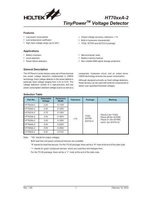
HT70xxA-2TinyPower TM Voltage DetectorSelection TableNote:²XX ²stands for output voltages.Both lead free and green compound devices are available.²#²stands for lead free devices.For the TO-92package,there will be a ²#²mark at the end of the date code.²+²stands for green compound devices,which are Lead-free and Halogen-free.For the TO-92package,there will be a ²+²mark at the end of the date code.Rev.1.001February 10,2012General DescriptionThe HT70xxA-2series devices area set of three terminal low power voltage detectors implemented in CMOS technology.Each voltage detector in the series detects a particular fixed voltage ranging from 2.2V to 8.2V.The voltage detectors consist of a high-precision and low power consumption standard voltage source as well as acomparator,hysteresis circuit,and an output driver.CMOS technology ensures low power consumption.Although designed primarily as fixed voltage detectors,these devices can be used with external components to detect user specified threshold voltages.Features·Low power consumption ·Low temperature coefficient ·Highinput voltage range (up to 24V)·Output voltage accuracy:tolerance ±1%·Built-in hysteresis characteristic ·TO92,SOT89and SOT23-5packageApplications·Battery checkers ·Level selectors ·Power failure detectors·Microcomputer reset ·Battery memory backup·Non-volatile RAM signal storage protectorsBlock DiagramN Channel Open Drain Output(Normal Open;Active Low)Output Table&CurvePin AssignmentRev.1.002February10,2012Absolute Maximum RatingsSupply Voltage.............................................................................................................................V SS-0.3V to V SS+26V Output Voltage...........................V SS-0.3V to V DD+0.3V Output Current......................................................50mA Storage Temperature............................-50°C to125°C Power Consumption..........................................200mW Operating Temperature...........................-40°C to85°CNote:These are stress ratings only.Stresses exceeding the range specified under²Absolute Maximum Ratings²may cause substantial damage to the device.Functional operation of this device at other conditions beyond those listed in the specification is not implied and prolonged exposure to extreme conditions may affect device reliability.Electrical CharacteristicsHT7022A-2Ta=25°CHT7024A-2Ta=25°CRev.1.003February10,2012HT7033A-2Ta=25°CHT7039A-2Ta=25°CRev.1.004February10,2012HT7050A-2Ta=25°CHT7082A-2Ta=25°CRev.1.005February10,2012Functional DescriptionThe HT70xxA-2series is a set of voltage detectors equipped with a high stability voltage reference which is connected to the negative input of a comparator¾denoted as V REF in the following figure for NMOS output voltage detector.When the voltage drop to the positive input of the comparator(i,e,V B)is higher than V REF,VOUT goes high,M1turns off,and V B is expressed as V BH=V DD´(R B+R C)/(R A+R B+R C).If V DD is decreased so that V B falls to a value less than V REF,the comparator output inverts from high to low,V OUT goes low,V C is high,M1 turns on,RC is bypassed,and V B becomes:V BL=V DD´R B/(R A+R B),which is less than V BH.By so doing,the comparator output will stay low to prevent the circuit from oscillating when V B»V REF.If V DD falls below the minimum operating voltage,the output becomes undefined.When VDD goes from low to V DD´R B/(R A+R B)>V REF,the comparator output and V OUT goes high.The detectable voltage is defined as:V DET(-)=R+R+RR+RA B CB C´V REFThe release voltage is defined as:V DET(+)=R+RRA BB´V REFThe hysteresis width is:V HYS=V DET(+)-V DET(-)The figure demonstrates the NMOS output type withpositive output polarity(V OUT is normally open,activelow).The HT70xxA-2series also supplies options forother output types with active high outputs.Applicationcircuits shown are examples of positive output polarity(normally open,active low)unless otherwise specified.NMOS Output Voltage DetectorRev.1.006February10,2012Application CircuitsRev.1.007February 10,2012Microcomputer Reset CircuitNormally a reset circuit is required to protect the microcomputer system from malfunctions due to power line interruptions.The following examples show how different output configurations perform a reset function in various systems.·NMOS open drain output application for separatepower supply·NMOS open drain output application with R-C delayPower-on Reset CircuitWith several external components,the NMOS open drain type of the HT70xxA-2series can be used to perform a power-on reset function as shown:5V Power Line Monitoring CircuitGenerally,a minimum operating voltage of 4.5V is guaranteed in a 5V power line system.The HT7044A-2is recommended for use as 5V power line monitoring circuit.·5V power line monitor with power-on reset·with5V voltage regulatorChange of Detectable VoltageIf the required voltage is not found in the standard product selection table,it is possible to change it by using external resistance dividers or diodes.·Varying the detectable voltage with a resistance di-viderDetectable voltage=R+RRA BB´V DETHysteresis width=R+RRA BB´V HYS·Varying the detectable voltage with a diode Detectable Voltage=V f1+V f2+V DET Malfunction AnalysisThe following circuit demonstrates the way a circuit analyzes malfunctions by monitoring the variation or spike noise of power supply voltage.Charge Monitoring CircuitThe following circuit shows a charged monitor for protection against battery deterioration by overcharging.When the voltage of the battery is higher than the set detectable voltage,the transistor turns on to bypass the charge current,protecting the battery from overcharging.Rev.1.008February10,2012Level SelectorThe following diagram illustrates a logic level selector.Rev.1.009February10,2012Package InformationNote that the package information provided here is for consultation purposes only.As this information may be updated at regular intervals users are reminded to consult the Holtek website(/english/literature/package.pdf)for the latest version of the package information.3-pin TO92Outline DimensionsRev.1.0010February10,2012Rev.1.0011February10,2012Rev.1.0012February10,2012Product Tape and Reel SpecificationsTO92Reel Dimensions(Unit:mm)Rev.1.0013February10,2012Reel DimensionsSOT89-3Rev.1.0014February10,2012Note:Thickness less than0.38±0.05mm~0.5mmP0Accumulated pitch tolerance:±1mm/20pitches.()Bracketed figures are for consultation onlyRev.1.0015February10,2012SOT89-3Rev.1.0016February10,2012Holtek Semiconductor Inc.(Headquarters)No.3,Creation Rd.II,Science Park,Hsinchu,TaiwanTel:886-3-563-1999Fax:886-3-563-1189Holtek Semiconductor Inc.(Taipei Sales Office)4F-2,No.3-2,YuanQu St.,Nankang Software Park,Taipei115,TaiwanTel:886-2-2655-7070Fax:886-2-2655-7373Fax:886-2-2655-7383(International sales hotline)Holtek Semiconductor Inc.(Shenzhen Sales Office)5F,Unit A,Productivity Building,No.5Gaoxin M2nd Road,Nanshan District,Shenzhen,China518057Tel:86-755-8616-9908,86-755-8616-9308Fax:86-755-8616-9722Holtek Semiconductor(USA),Inc.(North America Sales Office)46729Fremont Blvd.,Fremont,CA94538,USATel:1-510-252-9880Fax:1-510-252-9885CopyrightÓ2012by HOLTEK SEMICONDUCTOR INC.The information appearing in this Data Sheet is believed to be accurate at the time of publication.However,Holtek as-sumes no responsibility arising from the use of the specifications described.The applications mentioned herein are used solely for the purpose of illustration and Holtek makes no warranty or representation that such applications will be suitable without further modification,nor recommends the use of its products for application that may present a risk to human life due to malfunction or otherwise.Holtek¢s products are not authorized for use as critical components in life support devices or systems.Holtek reserves the right to alter its products without prior notification.For the most up-to-date information, please visit our web site at .Rev.1.0017February10,2012。
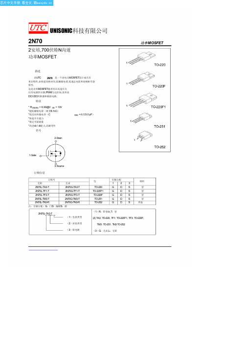
2N70中文资料(Unisonic Technologies)中文数据手册「EasyDatasheet - 矽搜」
VDS=560V, V GS=10V, I D=2.0A (注1,2)
VGS = 0 V, I SD = 2.0 A
VGS = 0 V, I SD = 2.0A di / dt = 100 A /μs(注1)
功 率 M OSFET
最小典型最大单位
700
V
10 μA
100 nA
-100 nA
0.4
V/°С
2.0
4.0 V
5.0 6.3 Ω
270 350 pF 38 50 pF 5 7 pF
芯片中文手册,看全文,戳
2N70
电气特性(续)
参数
开关特性 导通延迟时间 导通上升时间 关断延迟时间 关断下降时间 总栅极电荷 栅源充 栅漏极电荷
最小典型最大单位
30 ns
80 ns
50 ns
70 ns
8.1 11 nC
1.7
nC
4.4
nC
1.4 V
2.0 A
8.0 A
260
ns
1.09
μC
芯片中文手册,看全文,戳
2N70
测试电路和波形
D.U.T.
+
V
+
-
L
R
同类型
V
作为D.U.T.
司机
* dv / dt由R控制 * I 由脉冲周期控制 * D.U.T.-测试设备
功 率 M OSFET
V
V
(驱动器)
I (D.U.T.)
V (D.U.T.)
图 . 1A峰值二极管恢复 dv / dt测试电路
期
兄弟PT-70电子标签机使用手册说明书
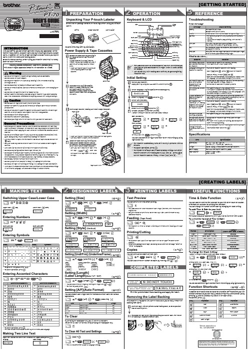
English / Français www.brother.ca
LW7595001 Printed in China
1 PREPARATION
Unpacking Your P-touch Labeler
Check that the package contains the followings before using your P-touch labeler.
Shift key Enter key Accent key Space key
• The LCD shows one row of 8 characters; however, the text that you enter can be up to 80 characters in length, which will scroll across the display.
beverages on to it. • Do not disassemble or modify the P-touch labeler/batteries. • Do not use metallic objects, such as tweezers or a metallic pen, when changing the
• Use Cursor key while holding down Shift key to go to beginning / end of the text.
Initial Setting
Turn on your machine. Supply power by using four AAA batteries, and then press .
安全技术说明书 Covi-ox T-70 EU

安全技术说明书页: 1/10 巴斯夫安全技术说明书日期 / 修订: 24.10.2016版本: 2.0产品: Covi-ox® T-70 EU(30533886/SDS_GEN_CN/ZH)印刷日期 03.11.20231. 物质/制剂及公司信息Covi-ox® T-70 EU推荐用途和限制用途: 抗氧化剂, 食品工业公司:巴斯夫(中国)有限公司中国上海浦东江心沙路300号邮政编码 200137电话: +86 21 20391000传真号: +86 21 20394800E-mail地址: **********************紧急联络信息:巴斯夫紧急热线中心(中国)+86 21 5861-1199巴斯夫紧急热线中心(国际):电话: +49 180 2273-112Company:BASF (China) Co., Ltd.300 Jiang Xin Sha RoadPu Dong Shanghai 200137, CHINA Telephone: +86 21 20391000Telefax number: +86 21 20394800E-mail address: ********************** Emergency information:Emergency Call Center (China):+86 21 5861-1199International emergency number: Telephone: +49 180 2273-1122. 危险性识别纯物质和混合物的分类:根据 GHS 标准,该产品不需要进行分类。
标签要素和警示性说明:根据GHS标准,该产品不需要添加危险警示标签巴斯夫安全技术说明书日期 / 修订: 24.10.2016版本: 2.0产品: Covi-ox® T-70 EU(30533886/SDS_GEN_CN/ZH)印刷日期 03.11.2023其它危害但是不至于归入分类:产品渗漏/溢出有高度致滑危险。
潘森高能电池产品安全数据表说明书
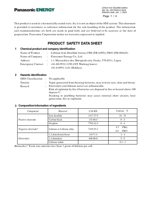
This product is used in a hermetically sealed state. So, it is not an object of the SDS system. This document is provided to customers as reference information for the safe handling of the product. The information and recommendations set forth are made in good faith and are believed to be accurate at the date of preparation. Panasonic Corporation makes no warranty expressed or implied.PRODUCT SAFETY DATA SHEET1 Chemical product and company identificationName of Product : Lithium Iron Disulfide battery FR6 (FR14505), FR03 (FR10G445)Name of Company : Panasonic Energy Co., Ltd.Address : 1-1Matsushita-cho, Moriguchi-city, Osaka, 570-8511, JapanEmergency Contact : +81-80-9932-3190 (JST Working hours)+81-6-6991-1141 (Holiday)2Hazards identificationGHS Classification : No applicableToxicity : Vapor generated from burning batteries, may irritate eyes, skin and throat.Hazard : Electrolyte and lithium metal are inflammable.Risk of explosion by fire if batteries are disposed in fire or heated above 100degrees C.Stacking or jumbling batteries may cause external short circuits, heatgeneration, fire or explosion.3Composition/information of ingredientsComponent Material CAS RN Content •i%•jPositive electrode Iron disulfide 1317-37-9 24 - 35 Carbon black 133-86-4 0 - 4 Graphite 7782-42-5 0 - 4Negative electrode* Lithium or Lithium alloy 7439-93-2 6.7 •iFR6) 6.6 •iFR03•jElectrolyte 1,2-dimethoxyethane 110-71-4 2 - 4 1,3-dioxolane 646-06-0 5 - 9 Lithium iodide - 0.3 - 3(Remarks) * Each size contains less than 1 gram of lithium per cell.4First aid measures (in case of electrolyte leakage from the battery)Eye contact : Flush the eyes with plenty of clean water for at least 15 minutesimmediately, without rubbing. Get immediate medical treatment.If appropriate procedures are not taken, this may cause eye injury.Skin contact : Wash the affected area under tepid running water using a mildsoap. If appropriates procedures are not taken, this may cause soreson the skin. Get medical attention if irritation develops or persists.Inhalation: Remove to fresh air immediately. Get medical treatmentimmediately.5 Firefighting measuresFire extinguishing agent : Alcohol-resistant foam and dry sand are effective.Extinguishing method : Be sure on the windward to extinguish the fire, since vapor maymake eyes, nose and throat irritate, Wear the respiratory protectionequipment in some cases.6Accidental release measures (in case of electrolyte leakage from the battery)Take up with absorbent cloth, treat cloth as inflammable.Move the battery away from the fire.7 Handling and storageHandling : žWhen packing the batteries, do not allow battery terminals tocontact each other, or contact with other metals. Be sure to packbatteries by providing partitions in the packaging box, or in aseparate plastic bag so that the single batteries are not mixedtogether.žUse strong material for packaging boxes so that they will not bedamaged by vibration, impact, dropping and stacking duringtheir transportation.žDo not short-circuit, recharge, deform, throw into fire ordisassemble.žDo not mix different type of batteries.žDo not solder directly onto batteries.žInsert the battery correctly in electrical equipment.Storage : •E Do not let water penetrate into packaging boxes during theirstorage and transportation.•E Do not store the battery in places of the high temperature orunder direct sunlight.žPlease also avoid the places of high humidity. Be sure not toexpose the battery to condensation, rain or frozen condition8.Exposure controls and personal protectionAcceptable concentration : Not specified about Lithium Battery.Facilities : Nothing in particularProtective Equipment (in case of electrolyte leakage from the battery)Respiratory Protection : For most condition no respiratory protection.Hand Protection : Safety gloves.Eye Protection : Safety goggle9.Physical and chemical propertiesAppearance : Cylindrical shapeNominal Voltage : 1.5 V10. Stability and reactivitySince batteries utilize a chemical reaction they are actually considered a chemical product.As such, battery performance will deteriorate over time even if stored for a long period of time without being used. In addition, the various usage conditions such as discharge, ambient temperature, etc. are not maintained within the specified ranges the life expectancy of the battery may be shortened or the device in which the battery is used may be damaged by electrolyte leakage.11.Toxicological informationSwallowing can lead to chemical bums, perforation of soft tissue, and death. Severe bums can occur within 2 hours of ingestion. Seek medical attention immediately.12.Ecological informationIn case of the worn out battery was disposed in land, the battery case may be corroded, and leak electrolyte. However, there is no environmental impact information.Mercury (Hg), Cadmium (Cd) and Lead (Pb) are not used in cell.13.Disposal considerationsWhen the battery is worn out, dispose of it under the ordinance of each local government.14.Transport informationHandlingDuring the transportation of a large amount of batteries by ship, trailer or railway, do not leave them in the places of high temperatures and do not allow them to be exposed to condensation.During the transportation do not allow packages to be dropped or damaged.Proper shipping name : Lithium metal batteriesUN Number, UN Class : UN3090, Class9 (for the Air transport by PI968 Section IA or IB): Exemption (for the Marine transport SP188 and the Air transportby Section II of PI 969 or 970)Even though the cells are classified as lithium metal batteries(UN3090 or UN3091), they are not subject to some requirements ofDangerous Goods Regulations because they meet the following:1. for cells, the lithium content is not more than 1 g ;2. each cell is of the type proven to meet the requirements of each test inthe UN Manual of T ests and Criteria, PartúL, sub-section 38.3.3. each cell is manufactured in ISO9001 certified factory.4. the test summary is available from;https:///ww/downloads/battery-test-summary Please refer to the following reference information about concrete ways of transportation. Actual content of packaging label and shipping documents varies by shipping companies. Make sure to confirm in advance with your shipping company.Information of referenceReference Packing Instruction(PI)/Special provision(SP)NoteAir transport IATA DGR PI 968 SectionúJ A Cells, Cargo Aircraft only; Net quantity perpackage Max. 35kgPI 968 SectionúJ B Cells, Cargo Aircraft only; net quantity perpackage Max. 2.5kgPI 969 SectionúK Cells packed with equipmentPI 970 SectionúK Cells contained in equipment Marine transport IMDG Code SP 18815.Regulatory information•E IATA Dangerous Goods Regulations Edition 64 (IATA DGR)•E IMO International Maritime Dangerous Goods Code 2020 and 2022 Edition (IMDG Code)•E UN Recommendations on the Transportation of Dangerous Goods, Model Regulations•E UN Recommendations on the Transportation of Dangerous Goods, Manual of Tests and Criteria •E EU Battery Directive•i2006/66/EC, 2013/56/EU)•E Regulation (EC) No. 1907/2006 on the Registration, Evaluation, Authorization and Restriction of Chemicals (REACH)•E State of California Regulations - Best management practices for Perchlorate Materials•E Act on Preventing Environmental Pollution of Mercury (Japan)16.Other informationThis PSDS is provided to customers as reference information in order to handle batteries safely.It is necessary for the customer to take appropriate measures depending on the actual situation such as the individual handling, based on this information.Prepared by: Engineering DepartmentEnergy Device Business DivisionPanasonic Energy Co., Ltd.。
HA17082资料

To VCC
To VCC
VCC Vout
VEE
Offset Null (N1)
Offset Null (N2)
HA17083 only Note: The HA17080 does not have an internal phase compensation capacitor.
3
HA17080 Series
Input noise voltage Vn
—
35
—
—
35
—
nV/√Hz RS = 100 Ω, f = 1 kHz
Notes: 1. The non-A ratings apply to the HA17080, HA17082, HA17083, and HA17084.
The A version ratings apply to the HA17080A, HA17082A, HA17083A, and HA17084A.
VCC 4 Vin(+)2 5 Vin(−)2 6
Vout2 7
1
4
−+
−+
2
3
(Top view)
−+ −+
14 Vout4 13 Vin(−)4 12 Vin(+)4 11 VEE 10 Vin(+)3 9 Vin(−)3 8 Vout3
2
Voltage Offset Test Circuit
HA17080 Series
Ordering Information
Item Number of operational amplifiers (number of channels) Offset adjustment pin Phase compensation type
Kromat KB系列色谱柱产品

国内外钽电容器型号对照表

-
小体积、大容量、漏电流小
非固体电解质钽电容器
(G)CA30
CA3、CAS、CDF、CA2
CL64/65
半密封、大容量、埋焊点结构
气密封高温非固体电解质钽 电容器
CA82
-
-
耐高温( 175 ℃ )
大容量非固体电解质钽电容器
CA32
CA3-46、CA30T
-
大容量、轴向或单向引出、并联结构
高压非固体电解质钽电容器
CA42
CA41A、CA400、CX
199D
小体积、高于GB7215-87 标准
CA421
-
-
超小体积
注:表中带有“ G ”产品型号表示既可秤“七专”,又可生产民品,如( G ) CA 型,其余依此类推。
41PS T370
大容量、矩形、单向引出
模压片式固体电解质钽电容器
CA45
CA45H、CX03
293D、
片式、高可靠
日立、TWC
CA45A
-
T491
片式、低 ESR
CA45B
-
T494
片式、超低 ESR
高频模压固体电解质钽电容器
CA471
-
-
高频、 8 或 16 只脚双列直插式
树脂包封固体电解质钽电容器
CA33A
CA-46、CDD3、CDD-4
CL14、CL17
高压、半密封、轴向或单向引出
钽箔电解电容器
CA12
-
-
小体积、大容量钽箔结构
双极性钽箔电解电容器
CA711
-
-
双极性、小体积、高压、钽箔结构
环氧树脂塑封模压固体电解质钽电容器
KD3002-DC70A中文资料
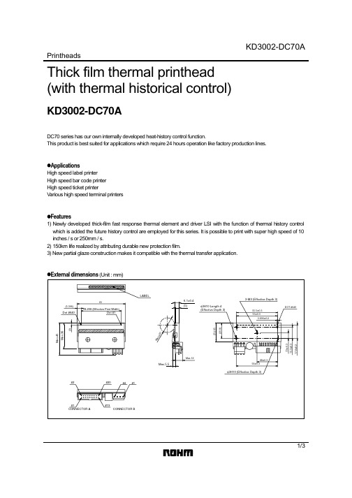
PrintheadsThick film thermal printhead(with thermal historical control)KD3002-DC70ADC70 series has our own internally developed heat-history control function.This product is best suited for applications which require 24 hours operation like factory production lines.z ApplicationsHigh speed label printerHigh speed bar code printerHigh speed ticket printerVarious high speed terminal printersz Features1) Newly developed thick-film fast response thermal element and driver LSI with the function of thermal history controlwhich is added the future history control are employed for this series. It is possible to print with super high speed of 10 inches / s or 250mm / s.2) 150km life realized by attributing durable new protection film.3) New partial glaze construction makes it compatible with the thermal transfer application.z External dimensions (Unit : mm)1/3Printheads2/3z Equivalent circuitV H (COM)V DD (+5)GND/ RESETCLK (CP)DODI/ LOAD / STB2/ STB1STARTINCTM TMSEL2SEL1DI No.DI640 ∼ 1DOT No.640 ∼ 257256 ∼ 1/ STB No./ STB2/ STB1DOT No.z Pin assignments/ RESET START DO NC TM TM / STB2/ STB1NC NCV H (COM)V H (COM)GND GND11121314151617181920No.CircuitNo.1234Circuit V DD V DD SEL2SEL1CLK (CP)NC DI NC INC / LOADNo.12345678910CircuitCONNECTOR A CONNECTOR BPrintheads3/3z CharacteristicsParameter−Rave V H P O 54.2080.08476401000240.550.416408φ20.0−−SLT −−mm mm dots ΩV W/dot ms dots MHz mm −150/(1×108)5 to 45−−km/pulses°CEffective printing width Symbol Typical Unit Average resistance value Dot pitch Total dot number Maximum number of dots energized simultaneously Maximum clock frequency Maximum roller diameter Running life / pulse life Operating temperatureApplied power Applied voltage Print cyclez Data sheetsENERGY (mJ/dot)Fig.2 Representative density curveO P T I C A L D E N S I T YSCANNING LINE TIME (ms)Fig.3 Maximum energy curveS U P P L Y E N E R G Y (M a x .) (m J /d o t )AppendixAbout Export Control Order in JapanProducts described herein are the objects of controlled goods in Annex 1 (Item 16) of Export T rade ControlOrder in Japan.In case of export from Japan, please confirm if it applies to "objective" criteria or an "informed" (by MITI clause)on the basis of "catch all controls for Non-Proliferation of Weapons of Mass Destruction.Appendix1-Rev1.1。
HT-69020NP-0, HT-69030NP-0 Duct Probe RH Transmitt

HT-69020NP-0, HT-69030NP-0 Duct Probe RHTransmitter Installation GuideIntroductionThe HT-69 Series Duct Probe Relative Humidity (RH)Transmitters use a highly accurate and reliable thermosetpolymer-based capacitance humidity sensor and state-of-the-art digital linearization and temperature-compensated circuitry to monitor humidity levels in a duct. The humidity sensor is encapsulated in a 60 micron HDPE filter at the end of a 9 in. (230 mm) stainless steel (S/S) probe and a compact enclosure.Figure 1: HT-69 Duct Probe RH Transmitter DimensionsFigure 2: Dimensions of the HT-69 Duct Probe RH Transmitter*241102556A*Part No. 24-11025-56 Rev. A2022-11-11MountingThe transmitter installs directly into any air duct with a minimum width or diameter of 10 in. (25.5 cm).-Select a suitable installation area in the middle of the duct wall.-To achieve the best reading, do not place in an area where air stratification may be present.-Mount the sensor at least 5 ft. (1.5 m) in either direction from elbows, dampers, filters, or other duct restrictions.-Avoid areas that expose the transmitter to vibrations or rapid temperature changes.To install the transmitter, complete the following steps:1.When you select a suitable spot, drill a 0.6 in. (15mm) to 0.75 in. (20 mm) hole for the probe.2.Slide the probe into the drilled hole until the enclosure is flush against the duct. The airflow direction is not important.3.Secure the enclosure to the duct with two No. 10 x 1 in. (25 mm) self-tapping screws (not provided).4.Tighten the screws until the enclosure is tight against the duct so that there is no movement of the enclosure. A foam gasket on the back of the enclosure provides a tight seal against any air leaks. See Step 1 in Figure 3.5.The enclosure includes a hinged cover with a latch.To open the cover, pull slightly on the latch on the right side of the enclosure. At the same time, pull on the cover as shown in Step 2 of Figure 3.6.A 0.5 in. NPT threaded connection hole is in the bottom of the enclosure. Screw the EMT or cable gland connector into the threaded connection holeuntil tight. See Step 3 in Figure 3.Note: Preferably use weatherproof EMT or cable gland fittings. The E-style enclosure includes 0.5 in. NPT to M16 thread adaptor and cable gland fitting.7.Make wire connections as shown in the wire diagram in Wiring .8.Swing the door closed until it securely latches. For added security, install the two provided screws in the integrated screw tabs. See Step 4 of Figure 3.Wiring•Deactivate the 24 VAC/DC power supply before you make all connections to the device to prevent electrical shock or equipment damage.•Use 14 AWG to 22 AWG shielded wiring for allconnections and do not locate the device wires in the same conduit with wiring that supplies inductive loads such as motors. Make all connections in accordance with national and local codes.•Pull at least 6 in. (15 cm) of wire into the enclosure,then complete the wiring connection according to the wire diagram for the applicable power supply and output signal type. See Figure 4.•Place the output switch in the required position to select the required signal output type (mA or VDC), as shown in Step 2 of Figure 4. The factory default setting is 4 mA to 20 mA.•If you select mA, no further output set up is required.If you select VOLT output as shown in Figure 5, place the voltage output switch to the required span position,that is 10 VDC = 0 VDC to 10 VDC. The factory default setting is 0 VDC to 10 VDC. See Step 1 of Figure 4.•Connect the DC positive or the AC voltage hot side to the PWR terminal. For voltage output or AC power,connect the supply common to the COM terminal.The device is reverse voltage-protected and does not operate if you connect it backwards. The device contains a half-wave power supply so the supplycommon is the same as the signal common. See Step 3of Figure 4.•The analog output is available on the OUT terminal.Check the controller Analog Input to determine the correct connection before you apply power as shown in Step 3 of Figure 4.Figure 3: Mounting the HT-69 Duct Probe RH TransmitterFigure 4: Wiring of the HT-60 Duct Probe TransmitterTechnical specificationsTable 1: HT-69020NP-0, HT-69030NP-0 Duct Probe RH Transmitter technical specificationsThe performance specifications are nominal and conform to acceptable industry standards. For application at conditions beyond these specifications, consult the local Johnson Controls office. Johnson Controls shall not be liable for damages resulting from misapplication or misuse of its products.Product warrantyThis product is covered by a limited warranty, details of which can be found at / buildingswarranty.Software termsUse of the software that is in (or constitutes) this product, or access to the cloud, or hosted services applicable to this product, if any, is subject to applicable end-user license, open-source software information, and other terms set forth at /techterms. Your use of this product constitutes an agreement to such terms. PatentsPatents: https://Single point of contactContact informationContact your local branch office: /locationsContact Johnson Controls: /contact-us© 2022 Johnson Controls. All rights reserved. All specifications and other information shown were current as of document revision and。
吉满生物科技(上海)有限公司产品说明书

产品手册H_HLA-G1 PDL1 MC38(mouse_PDL1 KO) Cell Line H_HLA-G1 PDL1 MC38(mouse_PDL1 KO)细胞系For research use only!本品仅供科研使用,严禁用于治疗!版本号:V2.8目录一、产品基本信息及组分 (3)二、包装、运输及储存 (3)三、材料准备 (3)1.细胞培养、冻存、复苏试剂准备 (3)2.试剂耗材准备 (3)四、细胞培养、复苏、冻存 (4)1.H_HLA-G1 PDL1 MC38(mouse_PDL1 KO) Cell Line细胞复苏 (4)2.H_HLA-G1 PDL1 MC38(mouse_PDL1 KO) Cell Line细胞传代 (4)3.H_HLA-G1 PDL1 MC38(mouse_PDL1 KO) Cell Line细胞冻存 (4)五、验证结果 (5)1.流式检测蛋白表达-HLA-G1 (5)2.流式检测蛋白表达-PDL1 (6)使用许可协议: (7)附录1 Mouse_PDL1敲除验证结果 (8)附录2 H_HLA-G1氨基酸序列(NP_002118.1) (9)附录3 H_PDL1氨基酸序列(NP_054862.1) (10)一、产品基本信息及组分基本信息产品编号产品名称规格GM-C22142H_HLA-G1 PDL1 MC38(mouse_PDL1 KO) Cell Line 1 kit产品组成产品编号产品名称规格数量储存GM-C24483H_HLA-G1 PDL1 MC38(mouse_PDL1 KO) Cell Line #45E6 Cells/mL1管-196℃GM-C24484H_HLA-G1 PDL1 MC38(mouse_PDL1 KO) Cell Line #55E6 Cells/mL1管-196℃Pen/Strep100 mL Thermo/15140-122Fetal Bovine Serum500 mL Thermo/10099141DMEM 500 mL gibco/C11995500BT/8122062Anti-H_CD274(PDL1) hIgG1 Antibody / Genomeditech/GM-31740ABAnti-H_HLA-G1 hIgG1 Antibody / Genomeditech/GM-28208AB细胞计数仪ThermoFisher Scientific/Countess 3流式细胞仪贝克曼库尔特国际贸易(上海)有限公司/CytoFLEX四、细胞培养、复苏、冻存1.H_HLA-G1 PDL1 MC38(mouse_PDL1 KO) Cell Line细胞复苏a)37℃水浴锅预热培养基,加入预热后的完全培养基5 mL至15 mL离心管。
深冷 DN350 电源使用说明书
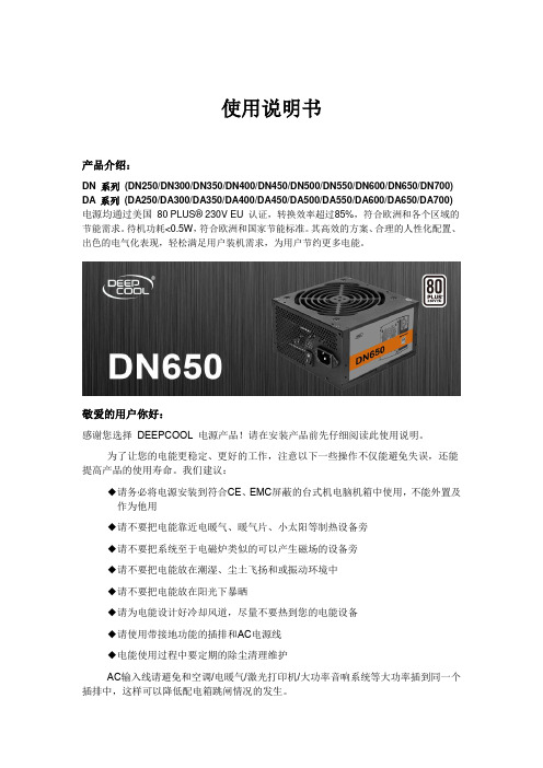
使用说明书产品介绍:DN 系列(DN250/DN300/DN350/DN400/DN450/DN500/DN550/DN600/DN650/DN700) DA 系列(DA250/DA300/DA350/DA400/DA450/DA500/DA550/DA600/DA650/DA700)电源均通过美国80 PLUS® 230V EU 认证,转换效率超过85%,符合欧洲和各个区域的节能需求。
待机功耗<0.5W,符合欧洲和国家节能标准。
其高效的方案、合理的人性化配置、出色的电气化表现,轻松满足用户装机需求,为用户节约更多电能。
敬爱的用户你好:感谢您选择DEEPCOOL 电源产品!请在安装产品前先仔细阅读此使用说明。
为了让您的电能更稳定、更好的工作,注意以下一些操作不仅能避免失误,还能提高产品的使用寿命。
我们建议:◆请务必将电源安装到符合CE、EMC屏蔽的台式机电脑机箱中使用,不能外置及作为他用◆请不要把电能靠近电暖气、暖气片、小太阳等制热设备旁◆请不要把系统至于电磁炉类似的可以产生磁场的设备旁◆请不要把电能放在潮湿、尘土飞扬和或振动环境中◆请不要把电能放在阳光下暴晒◆请为电能设计好冷却风道,尽量不要热到您的电能设备◆请使用带接地功能的插排和AC电源线◆电能使用过程中要定期的除尘清理维护AC输入线请避免和空调/电暖气/激光打印机/大功率音响系统等大功率插到同一个插排中,这样可以降低配电箱跳闸情况的发生。
产品特点◆符合INTEL ATX12V v 2.31标注;◆通过80 PLUS® 230V EU 认证—效率超过85%(50%负载下);◆双层EMI电路设计,在有效避免设备间的干扰的同时并保证电源可以优质的输出电流;◆加长线材设计,方便用户装机理线;◆120mm 智能温控风扇,有效做到散热和静音的平衡;◆智能节能芯片,待机功耗<0.5W,符合欧洲Erp要求;◆保护齐全—过电压,低电压,短路,超负载;◆支持多路SLI / 交火(DN500/DN550/DN600/DN650/DN700/DA500/DA550/DA600/DA650/DA700) ,和多核CPU;◆MTBF 高达120,000 小时输出参数◆请查看电源包装的参数表或产品铭牌.接头情况Mainboard (24P)请接入ATX/EEB/CEB server/workstation主板的24P接口中。
ATT7022E用户手册中文版
ATT7022E 用户手册
量产版 Rev1.3
版权归钜泉光电科技(上海)股份有限公司所有
Page1 of 59
Rev1.3
Tel: 021-51035886 Fax: 021-50277833 Email: sales@ Web:
2.1. PIN脚封装图 ..................................................................................................................................... 8 2.2. PIN脚功能说明 ................................................................................................................................. 8 2.3. 应用示意图 ..................................................................................................................................... 10 3. ATT7022E各模块描述.................................................................................................................................... 11 3.1. 电源检测电路 ...................
MJD350 300V PNP高电压传输器TO252(DPAK)商品说明书
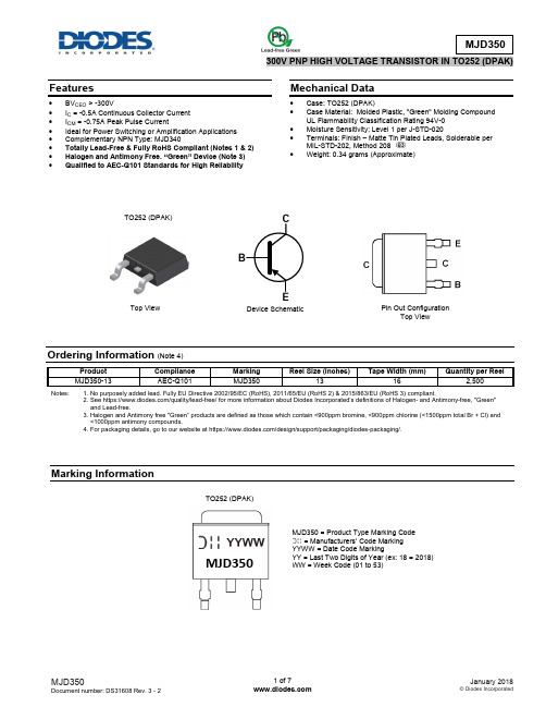
Features∙ BV CEO > -300V∙ I C = -0.5A Continuous Collector Current ∙ I CM = -0.75A Peak Pulse Current∙ Ideal for Power Switching or Amplification Applications ∙ Complementary NPN Type: MJD340∙ Totally Lead-Free & Fully RoHS Compliant (Notes 1 & 2) ∙ Halogen and Antimony Free. “Green” Device (Note 3) ∙ Qualified to AEC-Q101 Standards for High ReliabilityMechanical Data∙ Case: TO252 (DPAK)∙ Case Material: Molded Plastic, "Green" Molding Compound UL Flammability Classification Rating 94V-0 ∙ Moisture Sensitivity: Level 1 per J-STD-020∙ Terminals: Finish – Matte Tin Plated Leads, Solderable per MIL-STD-202, Method 208 ∙Weight: 0.34 grams (Approximate)Ordering Information (Note 4)Notes: 1. No purposely added lead. Fully EU Directive 2002/95/EC (RoHS), 2011/65/EU (RoHS 2) & 2015/863/EU (RoHS 3) compliant.2. See https:///quality/lead-free/ for more information about Diodes Incorporated’s definitions of Hal ogen- and Antimony-free, "Green" and Lead-free.3. Halogen and Antimony free "Green” products are defined as those which contain <900ppm bromine, <900ppm chlorine (<1500ppm tot al Br + Cl) and <1000ppm antimony compounds.4. For packaging details, go to our website at https:///design/support/packaging/diodes-packaging/.Marking InformationTop ViewDevice SchematicPin Out ConfigurationTop ViewMJD350 = Product Type Marking Code = Manufacturers’ Code Marking YYWW = Date Code MarkingYY = Last Two Digits of Year (ex: 18 = 2018) WW = Week Code (01 to 53)TO252 (DPAK)TO252 (DPAK)MJD350Thermal Characteristics(@T A = +25°C, unless otherwise specified.)Notes: 5. For a device mounted on FR-4 PCB with minimum recommended pad layout.6. Refer to JEDEC specification JESD22-A114 and JESD22-A115.Thermal Characteristics and Derating InformationElectrical Characteristics(@T A = +25°C, unless otherwise specified.)Note: 7. Measured under pulsed conditions. Pulse width ≤300μs. Duty cycle ≤2%.Typical Electrical Characteristics(@T A = +25°C, unless otherwise specified.)Package Outline DimensionsPlease see /package-outlines.html for the latest version.TO252 (DPAK)Suggested Pad LayoutPlease see /package-outlines.html for the latest version.TO252 (DPAK)Note:For high voltage applications, the appropriate industry sector guidelines should be considered with regards to creepage and clearance distances between device Terminals and PCB tracking.7°±1°Seating Plane。
Perkadox 16-GB70 产品数据册说明书
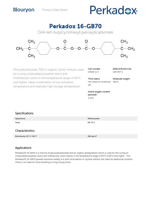
Product Data SheetPerkadox 16-GB70Di(4-tert-butylcyclohexyl) peroxydicarbonatePeroxydicarbonate, 70% in organic carrier mixture, used for curing unsaturated polyester resins and(meth)acrylic resins in the temperature range of 60°C and higher. Ideal combination of low activation temperature and relatively high storage temperature.CAS number15520-11-3EINECS/ELINCS No.239-557-1TSCA statusnot listed on inventoryyetMolecular weight398.5Active oxygen contentperoxide4.01%SpecificationsAppearance White powderAssay68-72 %CharacteristicsBulk density, 20 °C / 68 °F280 kg/m³ApplicationsPerkadox® 16-GB70 is a mixture of peroxydicarbonate and an organic phlegmatizer which is used for the curing of unsaturated polyester resins and methacrylic resins mainly in the temperature range of 60°C (140°F) and higher. The Perkadox® 16-GB70 powder dissolves readily in a resin formulation or styrene without the need for additional solvents. There is no need for extra handling or long mixing times.Half-life dataThe reactivity of an organic peroxide is usually given by its half-life (t1/2) at various temperatures. For Perkadox® 16-GB70 in chlorobenzene half-life at other temperatures can be calculated by using the equations and constants mentioned below:0.1 hr at 82°C (180°F)1 hr at 64°C (147°F)10 hr at 48°C (118°F)Formula 1kd = A·e-Ea/RTFormula 2t½ = (ln2)/kdEa126.39 kJ/moleA7.44E+15 s-1R8.3142 J/mole·KT(273.15+°C) KThermal stabilityOrganic peroxides are thermally unstable substances, which may undergo self-accelerating decomposition. The lowest temperature at which self-accelerating decomposition of a substance in the original packaging may occur is the Self-Accelerating Decomposition Temperature (SADT). The SADT is determined on the basis of the Heat Accumulation Storage Test.SADT40°C (104°F)Emergency temperature (Tₑ)35°C (95°F)Control temperature (Tc)30°C (86°F)Method The Heat Accumulation Storage Test is a recognized test method for thedetermination of the SADT of organic peroxides (see Recommendations on theTransport of Dangerous Goods, Manual of Tests and Criteria - United Nations, NewYork and Geneva).StorageDue to the relatively unstable nature of organic peroxides a loss of quality can be detected over a period of time. To minimize the loss of quality, Nouryon recommends a maximum storage temperatureTs Max.20°C (68°F)Note When stored under these recommended storage conditions, Perkadox® 16-GB70will remain within the Nouryon specifications for a period of at least 3 months afterdelivery.Packaging and transportThe standard packaging is a 25 lbs PE bag in a box. Both packaging and transport meet the international regulations. For the availability of other packed quantities contact your Nouryon representative. Perkadox® 16-GB70 is classified as Organic peroxide type D; solid, temperature controlled; Division 5. 2; UN 3116.Safety and handlingKeep containers tightly closed. Store and handle Perkadox® 16-GB70 in a dry well-ventilated place away from sources of heat or ignition and direct sunlight. Never weigh out in the storage room. Avoid contact with reducing agents (e. g. amines), acids, alkalis and heavy metal compounds (e. g. accelerators, driers and metal soaps). Please refer to the Safety Data Sheet (SDS) for further information on the safe storage, use and handling of Perkadox® 16-GB70. This information should be thoroughly reviewed prior to acceptance of this product.Major decomposition productsCarbon dioxide, 4-tert-Butyl-cyclohexanol, 4-tert-ButylcyclohexanoneAll information concerning this product and/or suggestions for handling and use contained herein are offered in good faith and are believed to be reliable.Nouryon, however, makes no warranty as to accuracy and/or sufficiency of such information and/or suggestions, as to the product's merchantability or fitness for any particular purpose, or that any suggested use will not infringe any patent. Nouryon does not accept any liability whatsoever arising out of the use of or reliance on this information, or out of the use or the performance of the product. Nothing contained herein shall be construed as granting or extending any license under any patent. Customer must determine for himself, by preliminary tests or otherwise, the suitability of this product for his purposes.The information contained herein supersedes all previously issued information on the subject matter covered. The customer may forward, distribute, and/or photocopy this document only if unaltered and complete, including all of its headers and footers, and should refrain from any unauthorized use. Don’t copythis document to a website.Trigonox and Perkadox® are registered trademarks of Nouryon Functional Chemicals B.V. or affiliates in one or more territories.Contact UsPolymer Specialties Americas************************Polymer Specialties Europe, Middle East, India and Africa*************************Polymer Specialties Asia Pacific************************2022-6-30© 2022Thermoset composites Perkadox 16-GB70。
- 1、下载文档前请自行甄别文档内容的完整性,平台不提供额外的编辑、内容补充、找答案等附加服务。
- 2、"仅部分预览"的文档,不可在线预览部分如存在完整性等问题,可反馈申请退款(可完整预览的文档不适用该条件!)。
- 3、如文档侵犯您的权益,请联系客服反馈,我们会尽快为您处理(人工客服工作时间:9:00-18:30)。
©1996The mark shows major revised points.MOS INTEGRATED CIRCUITDocument No. U11826EJ3V0DS00 (3rd edition)Date Published July 1997 N Printed in Japan2ORDERING INFORMATIONPart NumberPackageµPD703002GC-25-xxx-7EA 100-pin plastic QFP (fine pitch) (14 × 14 mm) (Resin thickness : 1.45 mm)µPD703002GC-25-xxx-8EU 100-pin plastic LQFP (fine pitch) (14 × 14 mm) (Resin thickness : 1.40 mm)Remarkxxx indicates the ROM code suffix.PIN CONFIGURATIONµPD703002P00 to P07:Port0A16 to A23:Address BusP10 to P17:Port1LBEN:Lower Byte EnableP20 to P27:Port2UBEN:Upper Byte EnableP30 to P37:Port3R/W:Read/Write StatusP40 to P47:Port4DSTB:Data StrobeP50 to P57:Port5ASTB:Address StrobeP60 to P67:Port6ST0, ST1:StatusP90 to P97:Port9HLDAK:Hold AcknowledgeP100 to P103:Port10HLDRQ:Hold RequestTO10, TO11:Timer Output CLKOUT:Clock OutputTCLR1:Timer Clear CKSEL:Clock SelectTI1:Timer Input PLLSEL:PLL SelectINTP00 to INTP03,:Interrupt Request From Peripherals WAIT:WaitINTP10 to INTP13MODE0, MODE1:ModeNMI:Non-maskable Interrupt Request RESET:ResetSO0 to SO2:Serial Output X1, X2:CrystalSI0 to SI2:Serial Input CV DD:Power Supply for Clock Generator :Serial Clock CV SS:Ground for Clock Generator TXD:Transmit Data V DD:Power SupplyRXD:Receive Data V SS:GroundAD0 to AD15:Address/Data Bus IC0:Internally Connected3FUNCTION BLOCK DIAGRAM4CONTENTS1.PIN FUNCTION LIST (7)1.1Port Pins (7)1.2Non-Port Pins (9)1.3Pin I/O Circuits and Recommended Connections of Unused Pins (11)2.FUNCTION BLOCKS (13)2.1Internal Units (13)2.1.1 CPU (13)2.1.2 Bus control unit (BCU) (13)2.1.3 ROM (13)2.1.4 RAM (13)2.1.5 Port (13)2.1.6 Interrupt controller (INTC) (13)2.1.7 Clock generator (CG) (13)2.1.8 Real-time pulse unit (RPU) (13)2.1.9 Serial interface (SIO) (14)3.CPU FUNCTION (15)3.1Features (15)4.BUS CONTROL FUNCTION (16)4.1Features (16)5.INTERRUPT/EXCEPTION HANDLING (17)5.1Features (17)5.2Configuration (17)6.CLOCK GENERATOR (19)6.1Features (19)6.2Configuration (19)7.TIMER/COUNTER FUNCTION (REAL-TIME PULSE UNIT) (20)7.1Features (20)7.2Configuration (21)8.SERIAL INTERFACE FUNCTION (SIO) (22)8.1Features (22)8.2Asynchronous Serial Interface (UART) (22)8.2.1 Features (22)8.2.2 Configuration (23)58.3 Clocked Serial Interface 0 to 2 (CSI0 to CSI2) (24)8.3.1 Features (24)8.3.2 Configuration (24)8.4 Baud Rate Generator 0, 1 (BRG0, BRG1) (25)8.4.1 Features (25)8.4.2 Configuration (25)9.PORT FUNCTION (26)9.1 Features (26)9.2 Configuration (26)10.RESET FUNCTION (38)10.1 Features (38)11.INSTRUCTION SET (39)11.1 Instruction Set List (39)12.ELECTRICAL SPECIFICATIONS (46)13.CHARACTERISTIC CURVES (REFERENCE) (65)14.PACKAGE DRAWINGS (66)15.RECOMMENDED SOLDERING CONDITIONS (68)671. PIN FUNCTION LIST1.1 Port Pins(1/2)Pin Name I/OFunctionAlternate Function P00I/OPort 0TO10P018-bit input/output portTO11P02Input/output can be specified bit-wise.TCLR1P03TI1P04INTP10P05INTP11P06INTP12P07INTP13P10 to P17I/OPort 1—8-bit input/output portInput/output can be specified bit-wise.P20Input Port 2NMI P21I/OP20 is the port for input onlyINTP00P22Operates as an NMI input when a valid edge is input.INTP01P23And shows NMI input status at bit 0 of P2 register.INTP02P24P21 to P27 are 7-bit input/output ports.INTP03P25Input/output can be specified bit-wise.SO2P26SI2P27SCK2P30I/OPort 3SO0P318-bit input/output portSI0P32Input/output can be specified bit-wise.SCK0P33TXD P34RXD P35SO1P36SI1P37SCK1P40 to P47I/OPort 4AD0 to AD78-bit input/output portInput/output can be specified bit-wise.P50 to P57I/O Port 5AD8 to AD158-bit input/output portInput/output can be specified bit-wise.P60 to P67I/OPort 6A16 to A238-bit input/output portInput/output can be specified bit-wise.8(2/2)Pin NameI/O FunctionAlternate Function P90 I/OPort 9LBEN P918-bit input/output portUBEN P92Input/output can be specified bit-wise.R/W P93DSTB P94ASTB P95ST0P96ST1P97—P100I/OPort 10HLDAK P1014-bit input/output portHLDRQP102Input/output can be specified bit-wise.—P103—91.2 Non-Port Pins(1/2)Pin Name I/OFunctionAlternate Function TO10OutputPulse signal output of timer 1P00TO11P01TCLR1InputTimer 1 external clear signal input P02TI1Timer 1 external count clock inputP03INTP10Input External maskable interrupt request input, or timer 1 external capture trigger P04INTP11input (in common use)P05INTP12P06INTP13P07NMI Input Non-maskable interrupt request input P20INTP00InputExternal maskable interrupt request inputP21INTP01P22INTP02P23INTP03P24SO0Output CSI0 serial data transmission output P30SI0Input CSI0 serial data reception input P31SCK0I/O CSI0 serial clock I/OP32SO1Output CSI1 serial data transmission output P35SI1Input CSI1 serial data reception input P36SCK1I/O CSI1 serial clock I/OP37SO2Output CSI2 serial data transmission output P25SI2Input CSI2 serial data reception input P26SCK2I/O CSI2 serial clock I/OP27TXD Output UART serial data transmission output P33RXD Input UART serial data reception inputP34AD0 to AD7I/O16-bit multiplexed address/data bus when expanding memory externallyP40 to P47AD8 to AD15P50 to P57A16 to A23Output Higher address bus when expanding memory externally P60 to P67LBEN OutputExternal data bus lower byte enable signal output P90UBEN External data bus higher byte enable signal output P91R/W External read/write status output P92DSTB External data strobe signal output P93ASTB External address strobe signal output P94ST0External bus cycle status outputP95ST1P96HLDAK Output Bus hold acknowledge output P100HLDRQ Input Bus hold request input P101CLKOUT Output System clock output—CKSEL Input Clock generator operation mode specification —PLLSELInputInput specifying PLL multiplication coefficient input—10(2/2)Pin Name I/OFunctionAlternate FunctionWAIT Input Bus cycle wait insertion control signal input —MODE0, MODE1Input Operation mode specification —RESET Input System reset input—X1Input Connect resonator for system clock. Input external clock to X1.—X2——CV DD —Positive power for internal clock generator —CV SS —Ground potential for internal clock generator —V DD —Positive power supply —V SS —Ground potential —IC0—Internally connected—1.3 Pin I/O Circuits and Recommended Connections of Unused PinsTable 1-1 shows the I/O circuit types of the respective pins in the normal operation mode and recommended connections of unused pins. Figure 1-1 shows the respective circuit types partially simplified.When connecting a pin to V DD or V SS via resistor, use of a resistor of 3 to 10 kΩ is recommended.Table 1-1. Types of Pin I/O Circuits and Recommended Connections of Unused PinsPin Name I/O Circuit Type Recommended ConnectionsP00/TO10, P01/TO115Input: Individually connect to V DD or V SS via resistor P02/TCLR1, P03/TI1,8Output: OpenP04/INTP10 to P07/INTP13P10 to P175P20/NMI2Directly connect to V SSP21/INTP00 to P24/INTP038Input: Individually connect to V DD or V SS via resistor P25/SO25Output: OpenP26/SI2, P27/SCK28P30/SO05P31/SI0, P32/SCK08P33/TXD, P34/RXD, P35/SO15P36/SI1, P37/SCK18P40/AD0 to P47/AD75P50/AD8 to P57/AD15P60/A16 to P67/A23P90/LBENP91/UBENP92/R/WP93/DSTBP94/ASTBP95/ST0, P96/ST1P97P100/HLDAKP101/HLDRQP102, P103CLKOUT3OpenCKSEL2—PLLSEL2—WAIT1Directly connect to V DDMODE0, MODE12—RESETIC0—Directly connect to V SSCV DD—Directly connect to V DDCV SS—Directly connect to V SSFigure 1-1. Pin I/O Circuits2. FUNCTION BLOCKS2.1 Internal Units2.1.1 CPUMost instructions, such as address calculation, arithmetic and logic operation, and data transfer, are executed in one clock cycle under control of 5-stage pipeline.The CPU also includes dedicated hardware such as a multiplier (16 by 16) and a 32-bit barrel shifter, aiming at processing complex instructions at high speeds.In addition, the CPU can access internal ROM (90 Kbytes) and RAM (3 Kbytes) in one clock cycle.2.1.2 Bus control unit (BCU)The BCU initiates necessary external bus cycles based on the physical address given by the CPU. When an instruction fetch of external memory is executed, if no bus cycle initiation is requested by the CPU, the BCU creates a prefetch address to prefetch an instruction code. The prefetched instruction code is taken into the internal instruction queue.2.1.3 ROMThe ROM has a capacity of 90 Kbytes and is mapped from the address 00000000H. Access to the ROM is enabled/disabled by setting the MODE0 and MODE1 pins.The CPU can access any address of the ROM in one clock cycle (to fetch an instruction).2.1.4 RAMThis RAM has a capacity of 3 Kbytes and is mapped from address FFFFE000H. The CPU can access any address of the RAM in one clock cycle (to access data).2.1.5 PortThe µPD703000 is provided with a total of 68 input/output port pins (of which one is an input port pin), or ports 0 through 10. These port pins can be used as the control pins.2.1.6 Interrupt controller (INTC)The interrupt controller controls various interrupt requests (NMI, INTP00-INTP03, and INTP10-INTP13) issued by peripheral hardware or external devices. Up to eight levels of interrupt priority can be individually specified for each interrupt request. In addition, multiplexed processing control can be performed.2.1.7 Clock generator (CG)The clock generator generates a CPU operating clock whose frequency is 1 or 5 times as high as (with the internal PLL) or half (without the internal PLL) the frequency of the resonator connected across the X1 and X2 pins. Instead of connecting a resonator, a clock signal can be input from off-chip.2.1.8 Real-time pulse unit (RPU)The RPU which includes a 16-bit timer/event counter and a 16-bit interval timer, measures pulse intervals and pulse frequency, and outputs programmable pulses.2.1.9 Serial interface (SIO)The serial interface includes one UART channel (asynchronous serial interface) and three CSI channels (clocked serial interface).The UART transfers data with the TXD and RXD pins. The baud rate is generated by an on-chip dedicated baud rate generator. The CSI transfers data with the SO0 to SO2, SI0 to SI2, and SCK0 to SCK2 pins. The baud rate can be generated from an on-chip dedicated baud rate generator, or supplied from off-chip.3. CPU FUNCTIONThe CPU of the µPD703002 is based on the RISC architecture and executes almost all the instructions in one clock cycle, using a 5-stage pipeline.3.1 Features•Minimum instruction execution time: 40 ns (@ internal 25-MHz operation)•Address space: 16-Mbyte linear•General registers: 32 bits × 32•Internal 32-bit architecture•Five-stage pipeline control•Multiply/divide instruction•Saturated operation instruction•32-bit shift instruction: 1 clock•Long/short format•Internal memory•ROM: 90 Kbytes•RAM: 3 Kbytes•Bit manipulate instructions: 4 types•Set•Clear•Not•Test4. BUS CONTROL FUNCTION4.1 Features•External device connectable with port pins (using alternate function)•Wait function•Programmable wait function inserting up to 3 states per 2 blocks •External wait function effected by WAIT pin•Idle state inserting function•Bus arbitration function•Bus hold function5. INTERRUPT/EXCEPTION HANDLING5.1 Features•Interrupts•Non-maskable:1 source•Maskable:16 sources•8-level programmable priority control•Multiplexed processing control according to priority•Masking each maskable interrupt request•Valid edge specification for external interrupt request •Exceptions•Software exception:32 sources•Exception trap:1 source (illegal instruction code exception) 5.2 ConfigurationXX: Identification name for each peripheral unit (OV, P1, CM, CS, SE, SR, ST, P0, CS) n : Peripheral unit number (0 to 4)Table 5-1. InterruptsInterrupt/Exception CausesDefault Exception Handler RestoreType ClassNameControlGeneration CauseGeneratingRegister UnitPriority Code Address PCReset Interrupt RESET—Reset input——0000H00000000H Undefined Non-maskable Interrupt NMI—NMI input——0010H00000010H next PC Software exception Exception TRAP0n Note—TRAP instruction——004n Note H00000040H next PC Exception TRAP1n Note—TRAP instruction——005n Note H00000050H next PC Exception trap Exception ILGOP—Illegal instruction code——0060H00000060H next PC Maskable Interrupt INTOV1OVIC1Timer 1 overflow RPU00080H00000080H next PC Interrupt INTP10/INTCC10P1IC0Match of INTP10 & CC10Pin/RPU10090H00000090H next PCInterrupt INTP11/INTCC11P1IC1Match of INTP11 & CC11Pin/RPU200A0H000000A0H next PCInterrupt INTP12/INTCC12P1IC2Match of INTP12 & CC12Pin/RPU300B0H000000B0H next PCInterrupt INTP13/INTCC13P1IC3Match of INTP13 & CC13Pin/RPU400C0H000000C0H next PCInterrupt INTCM4CMIC4Match of CM4RPU500D0H000000D0H next PCInterrupt INTCSI0CSIC0CSI0 transmit/receive SIO600E0H000000E0H next PCcompletionInterrupt INTSER0SEIC0UART0 receive error SIO700F0H000000F0H next PCInterrupt INTSR0SRIC0UART0 receive completion SIO80100H00000100H next PCInterrupt INTST0STIC0UART0 transmit completion SIO90110H00000110H next PCInterrupt INTP00P0IC0INTP00 pin Pin100120H00000120H next PCInterrupt INTP01P0IC1INTP01 pin Pin110130H00000130H next PCInterrupt INTP02P0IC2INTP02 pin Pin120140H00000140H next PCInterrupt INTP03P0IC3INTP03 pin Pin130150H00000150H next PCInterrupt INTCSI1CSIC1CSI1 transmit/receive completion SIO140160H00000160H next PCInterrupt INTCSI2CSIC2CSI2 transmit/receive completion SIO150170H00000170H next PC Note The "n" in the "Software exception" rows is a value from 0 to FH.Remarks1.Default priority:Priority used when two or more maskable interrupt requests having thesame priority are simultaneously generated. 0 indicates the highestpriority.Restore PC:PC value saved to EIPC or FEPC when interrupt/exception processing is started.However, the restore PC value saved if an interrupt is accepted while the DIVH(division) instruction is being executed is the PC value of the current instruction(DIVH).2.The execution address of an illegal instruction when an illegal instruction code exceptionoccurs can be calculated as (restore PC–4).6. CLOCK GENERATOR6.1 Features•Multiply function by PLL clock synthesizer (f XX = φ or f XX = φ/5)•Direct mode directly to input external clock•Power save mode•HALT mode•IDLE mode•Software STOP mode•Clock output inhibit function6.2 Configuration7. TIMER/COUNTER FUNCTION (REAL-TIME PULSE UNIT)7.1 Features•Pulse interval and frequency measurement and output of programmable pulse •16-bit measurement possible•Pulse can be generated in various shapes (interval pulse, one-shot pulse)•Timer 1•16-bit timer/event counter•Sources of count clock: 2 types (divided system clock or external pulse input)•Capture/compare registers: 4•Count clear pin: TCLR1•Interrupt sources: 5•External pulse output: 2•Timer 4•16-bit interval timer•Count clock selected from divided system clock•Compare register: 1•Interrupt source: 17.2 Configuration(1)Timer 1 (16-bit timer/event counter)(2)Timer 4 (16-bit interval timer)TM4 (16 bits)CM4Clear & startINTCM4Notem/16m/32φφm φ/2 /4 /8φφφNote Internal count clockRemark indicates the system clock.φ8. SERIAL INTERFACE FUNCTION (SIO)8.1 FeaturesThe µPD703002 is provided with four independent serial interface channels.(1)Asynchronous serial interface (UART): 1 channel(2)Clocked synchronous serial interface (CSI0 to CSI2): 3 channels8.2 Asynchronous Serial Interface (UART)8.2.1 Features•Transfer rate: 110 to 38400 bps (with BRG, when φ = 25 MHz)Up to 781 Kbps (with φ/2, when φ = 25 MHz)•Full-duplex communication•2-pin configurationTXD: Transmit data output pinRXD: Receive data input pin•Receive error detection function•Parity error•Framing error•Overrun error•Three interrupt sources•Receive error interrupt (INTSER0)•Reception completion interrupt (INTSR0)•Transmission completion interrupt (INTST0)•Character length of transmission/reception data is specified by setting ASIM00, ASIM01 register.•Character length:7, 8 bits9 bits (with extended bit appended)•Parity function:odd, even, 0, none•Transmission stop bit: 1 or 2 bits•Baud rate generatorRemarkφ indicates the system clock8.2.2 Configuration8.3 Clocked Serial Interface 0 to 2 (CSI0 to CSI2)8.3.1 Features•Number of channels: 3 (CSIn)•High-speed transfer rate6.25 Mbps MAX. (with φ/2, φ = 25 MHz)•Half-duplex communication•Data length of 8 bits•MSB first/LSB first can be switched for data•Selection of external serial clock input/internal serial clock output •Three pins usedSOn:Serial data output pinSIn:Serial data input pinSCKn:Serial clock I/O pin•Three interrupt sources•Interrupt request signal (INTCSIn)Remark1. φ indicates the system clock.2. n = 0 to 28.3.2 Configuration8.4 Baud Rate Generator 0, 1 (BRG0, BRG1)8.4.1 Features• Serial clock selectable from baud rate generator output and φ (system clock)• Same baud rate for transmission/reception8.4.2 Configuration9. PORT FUNCTION9.1 FeaturesThe ports of the µPD703002 have the following features:•Number of port pinsInput port: 1I/O port: 67•Shared with I/O pins of other peripheral functions•Input/output specifiable bitwise•Noise elimination•Edge detection9.2 ConfigurationFigure 9-1. Block Diagram of P00, P01 (Port 0)Figure 9-2. Block Diagram of P02 to P07 (Port 0)Figure 9-3. Block Diagram of P10 to P17 (Port 1)Figure 9-4. Block Diagram of P20 (Port 2)Figure 9-5. Block Diagram of P21 to P24 (Port 2)Figure 9-6. Block Diagram of P25 (Port 2)Figure 9-8. Block Diagram of P27 (Port 2)Figure 9-9. Block Diagram of P30, P33, P35 (Port 3)Figure 9-10. Block Diagram of P31, P36 (Port 3)Figure 9-11. Block Diagram of P32, P37 (Port 3)Figure 9-12. Block Diagram of P34 (Port 3)Figure 9-13. Block Diagram of P40 to P47 (Port 4)Figure 9-14. Block Diagram of P50 to P57 (Port 5)Figure 9-15. Block Diagram of P60 to P67 (Port 6)Figure 9-16. Block Diagram of P90 to P97 (Port 9)Figure 9-17. Block Diagram of P100, P103 (Port 10)Figure 9-18. Block Diagram of P101 (Port 10)Figure 9-19. Block Diagram of P102 (Port 10)10. RESET FUNCTIONWhen the RESET signal is made low, the system is reset, and the on-chip hardware units are initialized. Initialize the contents of each register in the program as necessary.10.1 Features• Noise elimination circuit of analog delay (60 to 220 ns) provided to the reset pin11. INSTRUCTION SET11.1 Instruction Set List•How to read instruction set listTable 11-1. Symbols Shown in "Operand" ColumnSymbol Descriptionreg1General register (used as source register)reg2General register (mainly used as destination register. Some are also used as source registers)ep Element pointerbit#33-bit data for bit number specification immX X-bit immediate dispX X-bit displacement regID System register numbervector 5-bit data specifying trap vector (00H through 1FH)cccc4-bit data indicating condition codeTable 11-2. Symbols Shown in “Operation Code” ColumnSymbol MeaningR1-bit-wise data of code specifing reg1 or regIDr1-bit-wise data of code specifing reg2d1-bit-wise data of displacementi1-bit-wise data of immediatecccc4-bit data indicating condition codebbb3-bit data specifing bit numberTable 11-3. Symbols Shown in "Operation" ColumnSymbol Meaning←AssignmentGR [ ]General registerSR [ ]System registerzero-extend (n)Zero-extends "n" to word lengthsign-extend (n)Sign-extends "n" to word lengthload-memory (a, b)Reads data of size "b" from address "a"store-memory (a, b, c)Writes data "b" of size "c" to address "a"load-memomy-bit (a, b)Reads bit "b" of address "a"store-memory-bit (a, b, c)Writes "c" to bit "b" of address "a"saturated (n)Performs saturated processing of n (n is 2's complement)"n" indicates result of operation.If "n" ≥ 7FFFFFFFH, 7FFFFFFFHIf "n" ≤ 80000000H, 80000000Hresult Reflects result on flagByte Byte (8 bits)Halfword Halfword (16 bits)Word Word (32 bits)+Add–Subtract||Bit concatenation×Multiply÷DivideAND Logical productOR Logical sumXOR Exclusive logical sumNOT Logical negationlogically shift left by Logical left shiftlogically shift right by Logical right shiftarithmetically shift right by Arithmetic right shiftTable 11-4. Symbols Shown in "Flag" ColumnIdentifier Meaning(blank)Not affected0Cleared to 0×Set or cleared according to resultR Value once saved is restoredTable 11-5. Condition CodesCondition Name (cond)Condition Code (cccc)Conditional Expression MeaningV0000OV = 1OverflowNV1000OV = 0No overflowC/L0001CY = 1CarryLower (Less than)NC/NL1001CY = 0No carryNot lower (Greater than or equal) Z/E0010Z = 1ZeroEqualNZ/NE1010Z = 0Not zeroNot equalNH0011(CY OR Z) = 1Not higher (Less than or equal) H1011(CY OR Z) = 0Higher (Greater than)N0100S = 1NegativeP1100S = 0PositiveT0101–Always (unconditional)SA1101SAT = 1SaturatedLT0110(S XOR OV) = 1Less than signedGE1110(S XOR OV) = 0Greater than or equal signedLE0111((S XOR OV) OR Z) = 1Less than or equal signedGT1111((S XOR OV) OR Z) = 0Greater than signedI n s t r u c t i o n G r o u pMnemonicOperandInstruction Set ListSLD.BSLD.H SLD.WLD.B LD.H LD.W SST.B SST.H SST.WST.B ST.H ST.W MOV MOV MOVHIMOVEA ADD ADD ADDISUB SUBRdisp7[ep], reg2disp8[ep], reg2disp8[ep], reg2disp16[reg1], reg2disp16[reg1], reg2disp16[reg1], reg2reg2, disp7[ep]reg2, disp8[ep]reg2, disp8[ep]reg2, disp16[reg1]reg2, disp16[reg1]reg2, disp16[reg1]reg1, reg2imm5, reg2imm16, reg1, reg2imm16, reg1, reg2reg1, reg2imm5, reg2imm16, reg1, reg2reg1, reg2reg1, reg2Operation CodeOperationadr ←ep+zero-extend(disp7)GR[reg2]←sign-extend(Load-memory(adr, Byte))adr ←ep+zero-extend(disp8)GR[reg2]←sign-extend(Load-memory(adr, Halfword))adr ←ep+zero-extend(disp8)GR[reg2]←Load-memory(adr, Word)adr ←GR[reg1]+sign-extend(disp16)GR[reg2]←sign-extend(Load-memory(adr, Byte))adr ←GR[reg1]+sign-extend(disp16)GR[reg2]←sign-extend(Load-memory(adr, Halfword))adr ←GR[reg1]+sign-extend(disp16)GR[reg2]←Load-memory(adr, Word)adr ←ep+zero-extend(disp7)Store-memory(adr, GR[reg2], Byte)adr ←ep+zero-extend(disp8)Store-memory(adr, GR[reg2], Halfword)adr ←ep+zero-extend(disp8)Store-memory(adr, GR[reg2], Word)adr ←GR[reg1]+sign-extend(disp16)Store-memory(adr, GR[reg2], Byte)adr ←GR[reg1]+sign-extend(disp16)Store-memory(adr, GR[reg2], Halfword)adr ←GR[reg1]+sign-extend(disp16)Store-memory(adr, GR[reg2], Word)GR[reg2]←GR[reg1]GR[reg2]←sign-extend(imm5)GR[reg2]←GR[reg1]+(imm16 || 016)GR[reg2]←GR[reg1]+sign-extend(imm16)GR[reg2]←GR[reg2]+GR[reg1]GR[reg2]←GR[reg2]+sign-extend(imm5)GR[reg2]←GR[reg1]+sign-extend(imm16)GR[reg2]←GR[reg2]–GR[reg1]GR[reg2]←GR[reg1]–GR[reg2]rrrrr0110dddddddrrrrr1000dddddddNote 1rrrrr1010dddddd0Note 2rrrrr111000RRRRR dddddddddddddddrrrrr111001RRRRR ddddddddddddddd0Note 3rrrrr111001RRRRR ddddddddddddddd1Note 3rrrrr0111ddddddd rrrrr1001dddddddNote 1rrrrr1010dddddd1Note 2rrrrr111010RRRRR ddddddddddddddddrrrrr111011RRRRR ddddddddddddddd0Note 3rrrrr111011RRRRR ddddddddddddddd1Note 3rrrrr000000RRRRR r r r r r 010000i i i i i rrrrr110010RRRRR i i i i i i i i i i i i i i i irrrrr110001RRRRR i i i i i i i i i i i i i i i irrrrr001110RRRRR rrrrr010010RRRRR rrrrr110000RRRRR i i i i i i i i i i i i i i irrrrr001101RRRRR rrrrr001100RRRRR A r i t h m e t i cL o a d /s t o r eFlagSATZSOVCY××××××××××××××××××××Notes 1.ddddddd = the higher 7 bits of disp82.dddddd = the higher 6 bits of disp83.ddddddddddddddd = the higher 15 bits of disp16MULH MULHMULHIDIVHCMP CMP SETFSATADD SATADD SATSUB SATSUBI SATSUBR TST OR ORIAND ANDI XOR XORI NOT SHL SHL SHR SHR SAR SAR GR[reg2]←GR[reg2]Note ×GR[reg1]Note (signed multiply)GR[reg2]←GR[reg2]Note ×sign-extend(imm5)(signed multiply)GR[reg2]←GR[reg2]Note×imm16(signed multiply)GR[reg2]←GR[reg2]÷GR[reg1]Note(signed divide)result ←GR[reg2]–GR[reg1]result ←GR[reg2]–sign-extend(imm5)if conditions are satisfied then GR[reg2]←00000001H else GR[reg2]←00000000H GR[reg2]←saturated(GR[reg2]+GR[reg1])GR[reg2]←saturated(GR[reg2]+sign-extend(imm5))GR[reg2]←saturated(GR[reg2]–GR[reg1])GR[reg2]←saturated(GR[reg1]–sign-extend(imm16))GR[reg2]←saturated(GR[reg1]–GR[reg2])result ←GR[reg2]AND GR[reg1]GR[reg2]←GR[reg2]OR GR[reg1]GR[reg2]←GR[reg1]OR zero-extend(imm16)GR[reg2]←GR[reg2]AND GR[reg1]GR[reg2]←GR[reg1]AND zero-extend(imm16)GR[reg2]←GR[reg2]XOR GR(reg1)GR[reg2]←GR[reg1]XOR zero-extend(imm16)GR[reg2]←NOT(GR[reg1])GR[reg2]←GR[reg2]logically shift left by GR[reg1]GR[reg2]←GR[reg2]logically shift left byzero-extend(imm5)GR[reg2]←GR[reg2]logically shift right by GR[reg1]GR[reg2]←GR[reg2]logically shift right byzero-extend(imm5)GR[reg2]←GR[reg2]arithmetically shift right by GR[reg1]GR[reg2]←GR[reg2]arithmetically shift right byzero-extend(imm5)I n s t r u c t i o n G r o u pMnemonicOperandreg1, reg2imm5, reg2imm16, reg1, reg2reg1, reg2reg1, reg2imm5, reg2cccc, reg2reg1, reg2imm5, reg2reg1, reg2imm16, reg1, reg2reg1, reg2reg1, reg2reg1, reg2imm16, reg1, reg2reg1, reg2imm16, reg1, reg2reg1, reg2imm16, reg1, reg2reg1, reg2reg1, reg2imm5, reg2reg1, reg2imm5, reg2reg1, reg2imm5, reg2Operation CodeOperationrrrrr000111RRRRR r r r r r 010111i i i i i rrrrr110111RRRRR i i i i i i i i i i i i i i irrrrr000010RRRRR rrrrr001111RRRRR r r r r r 010011i i i i i rrrrr1111110cccc 0000000000000000rrrrr000110RRRRR r r r r r 010001i i i i i rrrrr000101RRRRR rrrrr110011RRRRR i i i i i i i i i i i i i i i irrrrr000100RRRRR rrrrr001011RRRRR rrrrr001000RRRRR rrrrr110100RRRRR i i i i i i i i i i i i i i i irrrrr001010RRRRR rrrrr110110RRRRR i i i i i i i i i i i i i i i irrrrr001001RRRRR rrrrr110101RRRRR i i i i i i i i i i i i i i i irrrrr000001RRRRR rrrrr111111RRRRR 0000000011000000r r r r r 010110i i i i i rrrrr111111RRRRR 0000000010000000r r r r r 010100i i i i i rrrrr111111RRRRR 0000000010100000r r r r r 010101i i i i i A r i t h m e t i cS a t u r a t i o n o p e r a t i o nL o g i c a l o p e r a t i o nFlagSATZ S OV CY××××××××××××××××00000000000000×××××××××0××××××××××××××××××××××××××××××××××××××××××××Note Only the lower halfword data is valid.。
