2SD1223(TE16L1,NQ);中文规格书,Datasheet资料
常用场效应管和晶体管参数大全
常用场效应管和晶体管参数大全用户评论(1)关键字:晶体管参数(6)场效应管(6)常用场效应管和晶体管参数大全IRFU020 50V 15A 42W * * NMOS场效应?IRFPG42 1000V 4A 150W * * NMOS场效应?IRFPF40 900V 4.7A 150W * * NMOS场效应?IRFP9240 200V 12A 150W * * PMOS场效应?IRFP9140 100V 19A 150W * * PMOS场效应?IRFP460 500V 20A 250W * * NMOS场效应?IRFP450 500V 14A 180W * * NMOS场效应?IRFP440 500V 8A 150W * * NMOS场效应?IRFP353 350V 14A 180W * * NMOS场效应?IRFP350 400V 16A 180W * * NMOS场效应?IRFP340 400V 10A 150W * * NMOS场效应?IRFP250 200V 33A 180W * * NMOS场效应?IRFP240 200V 19A 150W * * NMOS场效应?IRFP150 100V 40A 180W * * NMOS场效应?IRFP140 100V 30A 150W * * NMOS场效应?IRFP054 60V 65A 180W * * NMOS场效应?IRFI744 400V 4A 32W * * NMOS场效应?IRFI730 400V 4A 32W * * NMOS场效应?IRFD123 80V 1.1A 1W * * NMOS场效应? IRFD120 100V 1.3A 1W * * NMOS场效应? IRFD113 60V 0.8A 1W * * NMOS场效应? IRFBE30 800V 2.8A 75W * * NMOS场效应? IRFBC40 600V 6.2A 125W * * NMOS场效应? IRFBC30 600V 3.6A 74W * * NMOS场效应? IRFBC20 600V 2.5A 50W * * NMOS场效应? IRFS9630 200V 6.5A 75W * * PMOS场效应? IRF9630 200V 6.5A 75W * * PMOS场效应? IRF9610 200V 1A 20W * * PMOS场效应? IRF9541 60V 19A 125W * * PMOS场效应? IRF9531 60V 12A 75W * * PMOS场效应? IRF9530 100V 12A 75W * * PMOS场效应? IRF840 500V 8A 125W * * NMOS场效应? IRF830 500V 4.5A 75W * * NMOS场效应? IRF740 400V 10A 125W * * NMOS场效应? IRF730 400V 5.5A 75W * * NMOS场效应? IRF720 400V 3.3A 50W * * NMOS场效应? IRF640 200V 18A 125W * * NMOS场效应? IRF630 200V 9A 75W * * NMOS场效应?IRF541 80V 28A 150W * * NMOS场效应?IRF540 100V 28A 150W * * NMOS场效应?IRF530 100V 14A 79W * * NMOS场效应?IRF440 500V 8A 125W * * NMOS场效应?IRF230 200V 9A 79W * * NMOS场效应?IRF130 100V 14A 79W * * NMOS场效应?BUZ20 100V 12A 75W * * NMOS场效应?BUZ11A 50V 25A 75W * * NMOS场效应?BS170 60V 0.3A 0.63W * * NMOS场效应常用场效应管及晶体管参数(2)?晶体管型号反压Vbe0 电流Icm 功率Pcm 放大系数特征频率管子类型? ???????2SC4582 600V 15A 75W * * NPN?2SC4517 550V 3A 30W * * NPN?2SC4429 1100V 8A 60W * * NPN?2SC4297 500V 12A 75W * * NPN?2SC4288 1400V 12A 200W * * NPN?2SC4242 450V 7A 40W * * NPN?2SC4231 800V 2A 30W * * NPN?2SC4111 1500V 10A 250W * * NPN?2SC4106 500V 7A 50W * 20MHZ NPN?2SC4059 600V 15A 130W * * NPN?2SC4038 50V 0.1A 0.3W * 180MHZ NPN? 2SC4024 100V 10A 35W * * NPN?2SC3998 1500V 25A 250W * * NPN?2SC3997 1500V 15A 250W * * NPN?2SC3987 50V 3A 20W 1000 * NPN(达林顿)? 2SC3953 120V 0.2A 1.3W * 400MHZ NPN? 2SC3907 180V 12A 130W * 30MHZ NPN? 2SC3893 1400V 8A 50W * 8MHZ NPN?2SC3886 1400V 8A 50W * 8MHZ NPN?2SC3873 500V 12A 75W * 30MHZ NPN?2SC3866 900V 3A 40W * * NPN?2SC3858 200V 17A 200W * 20MHZ NPN? 2SC3807 30V 2A 1.2W * 260MHZ NPN?2SC3783 900V 5A 100W * * NPN?2SC3720 1200V 10A 200W * * NPN?2SC3680 900V 7A 120W * * NPN?2SC3679 900V 5A 100W * * NPN?2SC3527 500V 15A 100W 13 * NPN?2SC3505 900V 6A 80W 12 * NPN?2SC3460 1100V 6A 100W 12 * NPN?2SC3457 1100V 3A 50W 12 * NPN?2SC3358 20V 0.15A * * 7000MHZ NPN?2SC3355 20V 0.15A * * 6500MHZ NPN?2SC3320 500V 15A 80W * * NPN?2SC3310 500V 5A 40W 20 * NPN?2SC3300 100V 15A 100W * * NPN?2SC1855 20V 0.02A 0.25W * 550MHZ NPN?2SC1507 300V 0.2A 15W * * NPN常用场效应管及晶体管参数(3)-------------------------------------------------------------------------------- ?晶体管型号反压Vbe0 电流Icm 功率Pcm 放大系数特征频率管子类型? ???????2SC1494 36V 6A 40W * 175MHZ NPN?2SC1222 60V 0.1A 0.25W * 100MHZ NPN?2SC1162 35V 1.5A 10W * * NPN?2SC1008 80V 0.7A 0.8W * 50MHZ NPN?2SC900 30V 0.03A 0.25W * 100MHZ NPN?2SC828 45V 0.05A 0.25W * * NPN?2SC815 60V 0.2A 0.25W * * NPN?2SC380 35V 0.03A 0.25W * * NPN?2SC106 60V 1.5A 15W * * NPN?2SB1494 120V 25A 120W * * PNP(达林顿)?2SB1429 180V 15A 150W * * PNP?2SB1400 120V 6A 25W 1000-20000 * PNP(达林顿)? 2SB1375 60V 3A 2W * * PNP?2SB1335 80V 4A 30W * * PNP?2SB1317 180V 15A 150W * * PNP?2SB1316 100V 2A 10W 15000 * PNP(达林顿)?2SB1243 40V 3A 1W * 70MHZ PNP?2SB1240 40V 2A 1W * 100MHZ PNP?2SB1238 80V 0.7A 1W * 100MHZ PNP?2SB1185 60V 3A 25W * 75MHZ PNP?2SB1079 100V 20A 100W 5000 * PNP(达林顿)?2SB1020 100V 7A 40W 6000 * PNP(达林顿)?2SB834 60V 3A 30W * * PNP?2SB817 160V 12A 100W * * PNP?2SB772 40V 3A 10W * * PNP?2SB744 70V 3A 10W * * PNP?2SB734 60V 1A 1W * * PNP?2SB688 120V 8A 80W * * PNP?2SB675 60V 7A 40W * * PNP(达林顿)? 2SB669 70V 4A 40W * * PNP(达林顿)? 2SB649 180V 1.5A 1W * * PNP?2SB647 120V 1A 0.9W * 140MHZ PNP? 2SB449 50V 3.5A 22W * * PNP?2SA1943 230V 15A 150W * * PNP?2SA1785 400V 1A 1W * 140MHZ PNP?2SA1668 200V 2A 25W * 20MHZ PNP?2SA1516 180V 12A 130W * 25MHZ PNP? 2SA1494 200V 17A 200W * 20MHZ PNP? 2SA1444 100V 1.5A 2W * 80MHZ PNP? 2SA1358 120V 1A 10W * 120MHZ PNP? 2SA1302 200V 15A 150W * * PNP?2SA1301 200V 10A 100W * * PNP?2SA1295 230V 17A 200W * * PNP?2SA1265 140V 10A 30W * * PNP?2SA1216 180V 17A 200W * * PNP-------------------------------------------------------------------------------- 常用场效应管及晶体管参数(4)-------------------------------------------------------------------------------- ?晶体管型号反压Vbe0 电流Icm 功率Pcm 放大系数特征频率管子类型? ???????2SA1162 50V 0.15A 0.15W * * PNP?2SA1123 150V 0.05A 0.75W * * PNP?2SA1020 50V 2A 0.9W * * PNP?2SA1009 350V 2A 15W * * PNP?2N6678 650V 15A 175W * * NPN?2N5685 60V 50A 300W * * NPN?2N6277 180V 50A 300W * * NPN?2N5551 160V 0.6A 0.6W * 100MHZ NPN?2N5401 160V 0.6A 0.6W * 100MHZ PNP?2N3773 160V 16A 150W * * NPN?2N3440 450V 1A 1W * * NPN?2N3055 100V 15A 115W * * NPN?2N2907 60V 0.6A 0.4W 200 * NPN?2N2369 40V 0.5A 0.3W * 800MHZ NPN?2N2222 60V 0.8A 0.5W 45 * NPN?9015 50V 0.1A 0.4W * 150MHZ PNP? 9014 50V 0.1A 0.4W * 150MHZ NPN? 9013 50V 0.5A 0.6W * * NPN?9012 50V 0.5A 0.6W * * PNP?9011 50V 0.03A 0.4W * 150MHZ NPN? TIP147 100V 10A 125W * * PNP?TIP142 100V 10A 125W * * NPN?TIP127 100V 8A 65W * * PNP?TIP122 100V 8A 65W * * NPN?TIP102 100V 8A 2W * * NPN?TIP42C 100V 6A 65W * * PNP?TIP41C 100V 6A 65W * * NPN?TIP36C 100V 25A 125W * * PNP?TIP35C 100V 25A 125W * * NPN?TIP32C 100V 3A 40W * * PNP?TIP31C 100V 3A 40W * * NPN?MJE13007 1500V 2.5A 60W * * NPN? MJE13005 400V 4A 60W * * NPN? MJE13003 400V 1.5A 14W * * NPN? MJE2955T 60V 10A 75W * * NPN?MJE340 300V 0.5A 20W * * NPN?MJ15025 400V 16A 250W * * PNP?MJ15024 400V 16A 250W * * NPN?MJ13333 400V 20A 175W * * NPN?MJ11033 120V 50A 300W * * NPN?MJ11032 120V 50A 300W * * NPN?MJ10025 850V 20A 250W * * NPN?MJ10016 500V 50A 200W * * NPN-------------------------------------------------------------------------------- 常用场效应管及晶体管参数(5)-------------------------------------------------------------------------------- ?晶体管型号反压Vbe0 电流Icm 功率Pcm 放大系数特征频率管子类型? ???????BUS13A 1000V 15A 175W * * NPN?BUH515 1500V 10A 80W * * NPN?BU2532 1500V 15A 150W * * NPN?BU2527 1500V 15A 150W * * NPN?BU2525 1500V 12A 150W * * NPN?BU2522 1500V 11A 150W * * NPN?BU2520 800V 10A 150W * * NPN?BU2508 700V 8A 125W * * NPN?BU2506 1500V 7A 50W * * NPN?BU932R 500V 15A 150W * * NPN?BU806 400V 8A 60W * * NPN?BU406 400V 7A 60W * * NPN?BU323 450V 10A 125W * * NPN(达林顿)? BF458 250V 0.1A 10W * * NPN?BD682 100V 4A 40W * * PNP?MJ10015 400V 50A 200W * * NPN?MJ10012 400V 10A 175W * * NPN(达林顿)? MJ4502 90V 30A 200W * * PNP?MJ3055 60V 15A 115W * * NPN?MJ2955 60V 15A 115W * * PNP?MN650 1500V 6A 80W * * NPN?BUX98A 400V 30A 210W * * NPN?BUX84 800V 2A 40W * * NPN?BUW13A 1000V 15A 150W * * NPN?BUV48A 450V 15A 150W * * NPN?BUV28A 225V 10A 65W * * NPN?BUV26 90V 14A 65W * * NPN?BUT12A 450V 10A 125W * * NPN?BUT11A 1000V 5A 100W * * NPN?BUS14A 1000V 30A 250W * * NPN?BD681 100V 4A 40W * * NPN?BD244 45V 6A 65W * * PNP?BD243 45V 6A 65W * * NPN?BD238 100V 2A 25W * * PNP?BD237 100V 2A 25W * * NPN?BD138 60V 1.5A 12.5W * * PNP?BD137 60V 1.5A 12.5W * * NPN?BD136 45V 1.5A 12.5W * * PNP?BD135 45V 1.5A 12.5W * * NPN?BC547 50V 0.2A 0.5W * 300MHZ NPN?BC546 80V 0.2A 0.5W * * NPN?BC338 50V 0.8A 0.6W * * NPN?BC337 50V 0.8A 0.6W * * NPN?BC327 50V 0.8 0.6W * * PNP?BC307 50V 0.2AA 0.3W * * PNP--------------------------------------------------------------------------------常用场效应管及晶体管参数(6)-------------------------------------------------------------------------------- ?晶体管型号反压Vbe0 电流Icm 功率Pcm 放大系数特征频率管子类型? ???????2SDK55 400V 4A 60W * * NPN?2SD2445 1500V 12.5A 120W * * NPN?2SD2388 90V 3A 1.2W * * NPN(达林顿)?2SD2335 1500V 7A 100W * * NPN?2SD2334 1500V 5A 80W * * NPN?2SD2156 120V 25A 125W 2000-20000 * NPN(达林顿)?2SD2155 180V 15A 150W * * NPN?2SD2036 60V 1A 1.2W * * NPN?2SD2012 60V 3A 2W * * NPN?2SD2008 80V 1A 1.5W * * NPN?2SD1997 40V 3A 1.5W * 100MHZ NPN?2SD1994 60V 1A 1W * * NPN?2SD1993 50V 0.1A 0.4W * * NPN?2SD1980 100V 2A 10W 1000-10000 * NPN(达林顿)?2SD1978 120V 1.5A 1W 30000 * NPN(达林顿)?2SD1975 180V 15A 150W * * NPN?2SD1930 100V 2A 1.2W 1000 * NPN(达林顿)?2SD1847 50V 1A 1W * * NPN(低噪)?2SD1762 60V 3A 25W * 90MHZ NPN?2SD1718 180V 15A 3.2W * 20MHZ NPN?2SD1640 120V 2A 1.2W 4000-40000 * NPN(达林顿)? 2SD1590 150V 8A 25W 15000 * NPN(达林顿)?2SD1559 100V 20A 20W 5000 * NPN(达林顿)?2SD1415 80V 7A 40W 6000 * NPN(达林顿)?2SD1416 80V 7A 40W 6000 * NPN(达林顿)?2SD1302 25V 0.5A 0.5W * 200MHZ NPN?2SD1273 80V 3A 40W * 50MHZ NPN?2SD1163A 350V 7A 40W * 60MHZ NPN?2SD1047 160V 12A 100W * * NPN?2SD1037 150V 30A 180W * * NPN?2SD1025 200V 8A 50W * * NPN(达林顿)?2SD789 100V 1A 0.9W * * NPN?2SD774 100V 1A 1W * * NPN?2SD669 180V 1.5A 1W * 140MHZ NPN?2SD667 120V 1A 0.9W * 140MHZ NPN( 达林顿)?2SD560 150V 5A 30W * * NPN( 达林顿)?2SD547 600V 50A 400W * * NPN?2SD438 500V 1A 0.75W * 100MHZ NPN?2SD415 120V 0.8A 5W * * NPN?2SD385 100V 7A 30W * * NPN( 达林顿)?2SD325 50V 3A 25W * * NPN?2SD40C 40V 0.5A 40W * * NPN( 达林顿)?2SC5252 1500V 15A 100W * * NPN?2SC5251 1500V 12A 50W * * NPN?2SC5250 1000V 7A 100W * * NPN-------------------------------------------------------------------------------- 常用场效应管及晶体管参数(7)-------------------------------------------------------------------------------- ?晶体管型号反压Vbe0 电流Icm 功率Pcm 放大系数特征频率管子类型? ???????2SC5244 1500V 15A 200W * * NPN?2SC5243 1500V 15A 200W * * NPN?2SC5207 1500V 10A 50W * * NPN?2sc5200 230V 15A 150W * * NPN?2sc5132 1500V 16A 50W * * NPN?2sc5088 1500V 10A 50W * * NPN?2sc5086 1500V 10A 50W * * NPN?2sc5020 1000V 7A 100W * * NPN?2sc4953 500V 2A 25W * * NPN?2sc4941 1500V 6A 65W * * NPN?2sc4927 1500V 8A 50W * * NPN?2sc4924 800V 10A 70W * * NPN?2sc4913 2000V 0.2A 35W * * NPN?2sc4769 1500V 7A 60W * * NPN( 带阻尼)? 2sc4747 1500V 10A 50W * * NPN?2sc4745 1500V 6A 50W * * NPN?2sc4742 1500V 6A 50W * * NPN( 带阻尼)? 2sc4706 900V 14A 130W * 6MH NPN?2SD1887 1500V 10A 70W * * NPN?2SD1886 1500V 8A 70W * * NPN?2SD1885 1500V 6A 60W * * NPN?2SD1884 1500V 5A 60W * * NPN?2SD1883 1500V 4A 50W * * NPN?2SD1882 1500V 3A 50W * * NPN?2SD1881 1500V 10A 70W * * NPN?2SD1880 1500V 8A 70W * * NPN?2SD1879 1500V 6A 60W * * NPN?2SD1876 1500V 3A 50W * * NPN?2SD1739 1500V 6A 100W * * NPN?2SD1738 1500V 5A 100W * * NPN?2SD1737 1500V 3.5A 60W * * NPN?2SD1732 1500V 7A 120W * * NPN?2SD1731 1500V 6A 100W * * NPN?2SD1730 1500V 5A 100W * * NPN?2SD1729 1500V 3.5A 60W * * NPN?2SD1711 1500V 7A 100W * * NPN?2SD1710 1500V 6A 100W * * NPN?2SD1656 1500V 6A 60W * * NPN?2SD1655 1500V 5A 60W * * NPN?2SD1654 1500V 3.5A 50W * * NPN?2SD1653 1500V 2.5A 50W * * NPN?2SD1652 1500V 6A 60W * * NPN?2SD1651 1500V 5A 60W * * NPN-------------------------------------------------------------------------------- 常用场效应管及晶体管参数(8)-------------------------------------------------------------------------------- ?晶体管型号反压Vbe0 电流Icm 功率Pcm 放大系数特征频率管子类型? ???????2SD1650 1500V 3.5A 50W * * NPN?2SD1635 1500V 5A 100W * * NPN?2SD1632 1500V 4A 70W * * NPN?2SD1577 1500V 5A 80W * * NPN?2SD1554 1500V 3.5A 40W * * NPN?2SD1548 1500V 10A 50W * * NPN?2SD1547 1500V 7A 50W * * NPN?2SD1546 1500V 6A 50W * * NPN?2SD1545 1500V 5A 50W * * NPN?2SD1456 1500V 6A 50W * * NPN?2SD1455 1500V 5A 50W * * NPN?2SD1454 1700V 4A 50W * * NPN?2SD1434 1700V 5A 80W * * NPN?2SD1431 1500V 5A 80W * * NPN?2SD1426 1500V 3.5A 80W * * NPN?2SD1402 1500V 5A 120W * * NPN?2SD1399 1500V 6A 60W * * NPN?2SD1344 1500V 6A 50W * * NPN?2SD1343 1500V 6A 50W * * NPN?2SD1941 1500V 6A 50W * * NPN? 2SD1911 1500V 5A 50W * * NPN? 2SD1341 1500V 5A 50W * * NPN? 2SD1219 1500V 3A 65W * * NPN? 2SD1290 1500V 3A 50W * * NPN? 2SD1175 1500V 5A 100W * * NPN? 2SD1174 1500V 5A 85W * * NPN? 2SD1173 1500V 5A 70W * * NPN? 2SD1172 1500V 5A 65W * * NPN? 2SD1143 1500V 5A 65W * * NPN? 2SD1142 1500V 3.5A 50W * * NPN? 2SD1016 1500V 7A 50W * * NPN? 2SD995 2500V 3A 50W * * NPN?2SD994 1500V 8A 50W * * NPN?2SD957A 1500V 6A 50W * * NPN? 2SD954 1500V 5A 95W * * NPN?2SD952 1500V 3A 70W * * NPN?2SD904 1500V 7A 60W * * NPN?2SD903 1500V 7A 50W * * NPN?2SD871 1500V 6A 50W * * NPN?2SD869 1500V 3.5A 50W * * NPN?2SD838 2500V 3A 50W * * NPN?2SD822 1500V 7A 50W * * NPN?2SD821 1500V 6A 50W * * NPN-------------------------------------------------------------------------------- 常用场效应管及晶体管参数(9)-------------------------------------------------------------------------------- ?晶体管型号反压Vbe0 电流Icm 功率Pcm 放大系数特征频率管子类型? ???????2SD348 1500V 7A 50W * * NPN?2SC4303A 1500V 6A 80W * * NPN?2SC4292 1500V 6A 100W * * NPN?2SC4291 1500V 5A 100W * * NPN?2SC4199A 1500V 10A 100W * * NPN?2SC3883 1500V 5A 50W * * NPN?2SC3729 1500V 5A 50W * * NPN?2SC3688 1500V 10A 150W * * NPN?2SC3687 1500V 8A 150W * * NPN?2SC3685 1500V 6A 120W * * NPN? 2SC3486 1500V 6A 120W * * NPN? 2SC3485 1500V 5A 120W * * NPN? 2SC3484 1500V 3.5A 80W * * NPN? 2SC3482 1500V 6A 120W * * NPN? 2SC3481 1500V 5A 120W * * NPN? 2SC3480 1500V 3.5A 80W * * NPN? 2SC2125 2200V 5A 50W * * NPN? 2SC2027 1500V 5A 50W * * NPN? BUY71 2200V 2A 40W * * NPN?BU508A 1500V 7.5A 75W * * NPN? BU500 1500V 6A 75W * * NPN?BU308 1500V 5A 12.5W * * NPN? BU209A 1700V 5A 12.5W * * NPN? BU208D 1500V 5A 12.5W * * NPN? BU208A 1500V 5A 12.5W * * NPN? BU108 1500V 5A 12.5W * * NPN?2SD1585 60V 3A 15W * * NPN?2SD773 20V 2A 1W * * NPN?2SC2785 60V 0.1A 0.3W * * NPN?2SD1246 30V 2A 0.75W * * NPN?2SC2570A 25V 0.07A 0.6W * * NPN?2SC1047 30V 0.015A 0.15W * * NPN?2SC3114 60V 0.15A 0.2W * * NPN?2SD400 25V 1A 0.75W * * NPN?2SC1923 40V 0.02A 0.1W * * NPN?2SC2621 300V 0.2A 10W * * NPN?2SC2568 300V 0.2A 10W * * NPN?2SC2216 50V 0.05A 0.3W * * NPN?2SC1674 30V 0.02A 0.1W * * NPN?2SC536F 40V 0.1A 0.25W * * NPN?2SA608F 30V 0.1A 0.25W * * PNP?2SD1271A 130V 7A 40W * * NPN?2SD1133 70V 4A 40W * * NPN-------------------------------------------------------------------------------- 常用场效应管及晶体管参数(10)-------------------------------------------------------------------------------- ?晶体管型号反压Vbe0 电流Icm 功率Pcm 放大系数特征频率管子类型????????2SC1890A 120V 0.05A 0.3W * * NPN? 2SC1360 50V 0.05A 0.5W * * NPN?2SA1304 150V 1.5A 25W * * PNP?2SD1274A 150V 5A 40W * * NPN?2SC2371 300V 0.1A 10W * * NPN?2SA966Y 30V 1.5A 0.9W * * PNP?2SD1378 80V 0.7A 10W * * NPN?2SD553Y 70V 7A 40W * * NPN?RN1204 50V 0.1A 0.3W * * NPN?2SD1405Y 50V 3A 30W * * NPN?2SC2878 50V 0.3A 0.4W * * NPN?2SC1959 30V 0.4A 0.5W * * NPN?2SC1569 300V 0.15A 1.5W * * NPN? 2SC2383Y 160V 1A 0.9W * * NPN?2SA1299 50V 0.5A 0.3W * * PNP?2SB564A 45V 0.05 0.25W * * PNP?2SD1877 800V 4A 50W * * NPN?BU508A 1500V 8A 125W * * NPN? BUT11 1500V 5A 80W * * NPN?2SD3505 900V 6A 50W * * NPN?2SD905 1400V 8A 50W * * NPN?2SC1942 1500V 3A 100W * * NPN? 2SD1397 1500V 3.5A 50W * * NPN? 2SD1396 1500V 2.5A 50W * * NPN? 2SC3153 900V 6A 100W * * NPN? 2SD1403 1500V 6A 50W * * NPN? 2SD1410 1500V 3.5A 80W * * NPN? 2SD2057 1500V 5A 100W * * NPN? 2SD2027 1500V 5A 50W * * NPN? 2SD953 1500V 7A 95W * * NPN?2SD951 1500V 3A 65W * * NPN?2SD950 1500V 3.5A 80W * * NPN? 2SD852 1500V 5A 70W * * NPN?2SD850 1500V 3A 25W * * NPN?2SD900B 1500V 5A 50W * * NPN? 2SD899A 1500V 4A 50W * * NPN? 2SD898B 1500V 3A 50W * * NPN? 2SD871 1500V 6A 50W * * NPN?2SD870 1500V 5A 50W * * NPN?2SD869 1500V 3.5A 50W * * NPN?2SD1432 1500V 6A 80W * * NPN?2SD1431 1500V 5A 80W * * NPN?2SD820 1500V 5A 50W * * NPN常用场效应管及晶体管参数(11)-------------------------------------------------------------------------------- ?晶体管型号反压Vbe0 电流Icm 功率Pcm 放大系数特征频率管子类型? ???????2SD819 1500V 3.5A 50W * * NPN?2SD1497 1500V 6A 50W * * NPN?2SD1398 1500V 5A 50W * * NPN?2SD1427 1500V 5A 80W * * NPN?2SD1428 1500V 6A 80W * * NPN?2SD1426 1500V 3.5A 80W * * NPN?2SC2068 70V 0.2A 0.62W * * NPN?2SC1627Y 80V 0.3A 0.6W * * NPN?2SC495Y 70V 0.8A 5W * * NPN?2SC388A 20V 0.02A 0.2W * * NPN?2SB686 100V 6A 60W * * PNP?2SA940 150V 1.5A 1.5W * * PNP?2SD1555 1500V 5A 50W * * NPN?2SD8806 60V 3A 30W * * NPN?2SC2456 300V 0.1A 10W * * NPN? 2SA1300 20V 2A 0.7W * * PNP?2SC304CD 60V 0.5A 0.8W * * NPN? 2SC2238 160V 1.5A 25W * * NPN? 2SC3328 80V 2A 0.9W * * NPN?2SC2190 450V 5A 100W * * NPN?2SA968Y 160V 1.5A 25W * * PNP?2SC3402 50V 0.1A 0.3W * * NPN?2SC2168 200V 2A 30W * * NPN?2SC3198G 60V 0.15A 0.4W * * NPN? 2SC2655Y 60V 2A 0.9W * * NPN?2SC1827 80V 4A 30W * * NPN?2SA1266Y 50V 0.15A 0.4W * * PNP? 2SD880 60V 3A 30W * * NPN?2SC1906 30V 0.05A 0.3W * * NPN? 2SC945 50V 0.1A 0.25W * * NPN?2SC3279 30V 2A 0.75W * * NPN?2SC2229 200V 0.05A 0.8W * * NPN?2SC383 20V 0.05A 0.2W * * NPN?2SA950Y 150V 0.8A 0.6W * * PNP?BC548B 30V 0.2A 0.5W * * NPN?2SC3399 50V 0.1A 0.3W * * NPN?2SD1455 1500V 5A 50W * * NPN?2SC1983R 80V 3A 30W * * NPN?2SC227 300V 0.1A 0.75W * * NPN?2SC1213D 50V 0.5A 0.4W * * NPN?2SA778AK 180V 0.05A 0.2W * * PNP?DTC114ES 50V 0.1A 0.25W * * NPN?2SC3413C 40V 0.1A 0.5W * * NPN常用场效应管及晶体管参数(12)---------------------------------------?晶体管型号反压Vbe0 电流Icm 功率Pcm 放大系数特征频率管子类型? ???????2SC2611 300V 0.1A 1.25W * * NPN?2SC1514 300V 0.1A 1.25W * * NPN?DTC124ES 50V 0.1A 0.25W * * PNP?2SD1078 50V 2A 20W * * NPN?2SD788 20V 2A 0.9W * * NPN?2SD882 40V 3A 10W * * NPN?2SD787 20V 2A 0.9W * * NPN?2SD401AK 200V 2A 25W * * NPN?2SC2610 300V 0.1A 0.8W * * NPN?2SC2271N 300V 0.1A 0.75W * * NPN? 2SC1740 50V 0.3A 0.3W * * NPN?2SC1214C 50V 0.5A 0.6W * * NPN?2SC458D 30V 0.1A 0.2W * * NPN?2SA673 50V 0.5A 0.4W * * PNP?2SD1556 1500V 6A 50W * * NPN?2SD1499 100V 5A 40W * * NPN?2SD1264A 200V 2A 30W * * NPN?2SD1010 50V 0.05A 0.3W * * NPN?2SD966 60V 5A 1W * * NPN?2SD601AR 60V 0.1A 0.2W * * NPN? 2SC3265Y 30V 0.8A 0.2W * * NPN?2SC3063 300V 0.1A 1.2W * * NPN?2SC2594 40V 5A 10W * * NPN?2SC1317-R 30V 0.5A 0.4W * * NPN?2SD1226 60V 3A 35W * * NPN?2SC2636Y 30V 0.05A 0.4W * * NPN?2SB940 200V 2A 30W * * PNP?2SA720-Q 50V 0.5A 0.4W * * PNP?2SD1391 1500V 5A 80W * * NPN?2SC2188 45V 0.05A 0.6W * * NPN?2SK301-R * 0.14A 0.25W * * N沟场效应管? 2SD1266 60V 3A 35W * * NPN?2SD1175 1500V 5A 100W * * NPN?2SD973 30V 1A 1W * * NPN?2SC2923 300V 0.2A 15W * * NPN?2SC2653H 250V 0.2A 15W * * NPN?2SC2377C 30V 0.15A 0.2W * * NPN?2SC1685Q 30V 0.1A 0.25W * * NPN?2SC1573A 250V 0.07A 0.6W * * NPN?2SB642-R 60V 0.2A 0.4W * * PNP?2SA1309A 25V 0.1A 0.3W * * PNP?2SA1018 150V 0.07A 0.75W * * PNP?2SA564A 25V 0.1A 0.25W * * PNP-------------------------------------------------------------------------------- 常用场效应管及晶体管参数(13)-------------------------------------------------------------------------------- ?晶体管型号反压Vbe0 电流Icm 功率Pcm 放大系数特征频率管子类型? ???????2SK301-Q * 0.14A 0.25W * * N沟场效应管?2SD1541 1500V 3A 50W * * NPN?2SC1685 30V 0.1A 0.25W * * NPN?2SC1573A 250V 0.07A 0.6W * * NPN?2SA1309A 25V 0.1A 0.3W * * PNP?UN4213 50V 0.1A 0.25W * * NPN?UN4211 50V 0.1A 0.25W * * NPN?UN4212 50V 0.1A 0.25W * * NPN?UN4111 50V 0.1A 0.25W * * PNP?2SD1541 1500V 3A 50W * * NPN?2SD965 40V 5A 0.75W * * NPN?2SC2839 30V 0.1A 0.1W * * NPN?2SC2258 250V 0.1A 1W * * NPN?2SC1846 45V 1A 1.2W * * NPN?2SC1573A 250V 0.07A 0.6W * * NPN?2SA1309A 25V 0.1A 0.3W * * PNP? 2SD1544 1500V 3.5A 40W * * NPN? 2SD802 900V 6A 50W * * NPN?2SC2717 35V 0.8A 7.5W * * NPN?2SC2482 150V 0.1A 0.9W * * NPN? 2SC2073 150V 1.5A 25W * * NPN? 2SC1815Y 60V 0.15A 0.4W * * NPN? 2SB774T 30V 0.01A 0.25W * * PNP? 2SA1015R 50V 0.15A 0.4W * * PNP? 2SA904 90V 0.05A 0.2W * * PNP?2SA562T 30V 0.4A 0.3W * * PNP?。
2SD1710中文资料(Wing Shing)中文数据手册「EasyDatasheet - 矽搜」
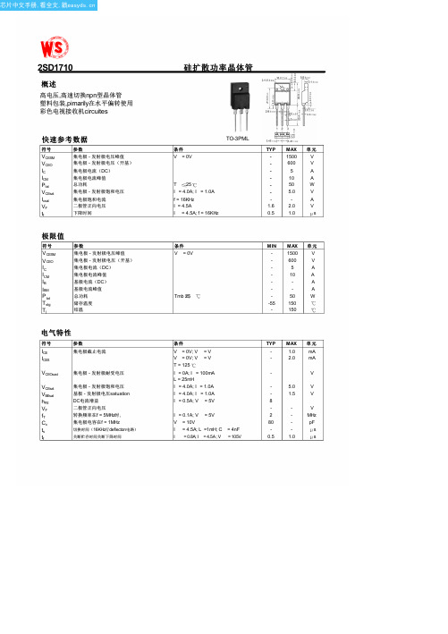
硅扩散功率晶体管
条件
V = 0V
TO-3PML
T 25 I = 4.0A; I = 1.0A f = 16KHz I = 4.5A I = 4.5A; f = 16KHz
TYP MAX 单元
-
1500
V
-
600
V
-
5
A
-
10
A
-
50
W
-
5.0
V
-
-
A
1.6
2.0
V
0.5
1.0
芯片中文手册,看全文,戳
2SD1710
概述
高电压,高速切换npn型晶体管 塑料包装,pimarily在水平偏转使用 彩色电视接收机circuites
快速参考数据
符号
VCESM VCEO IC ICM Ptot VCEsat Icsat VF tf
参数
集电极 - 发射极电压峰值 集电极 - 发射极电压(开基) 集电极电流(DC)
s
条件
V = 0V
Tmb 25
MIN MAX 单元
-
1500
V
-
600
V
-
5
A
-
10
A
-
-
A
-
-
A
-
50
W
-55 150
-
150
条件
V = 0V; V = V V = 0V; V = V T = 125 I = 0A; I = 100mA L = 25mH I = 4.0A; I = 1.0A I = 4.0A; I = 1.0A I = 0.5A; V = 5V
SD101CW(丝印S3)二极管规格书(含样品申请表)
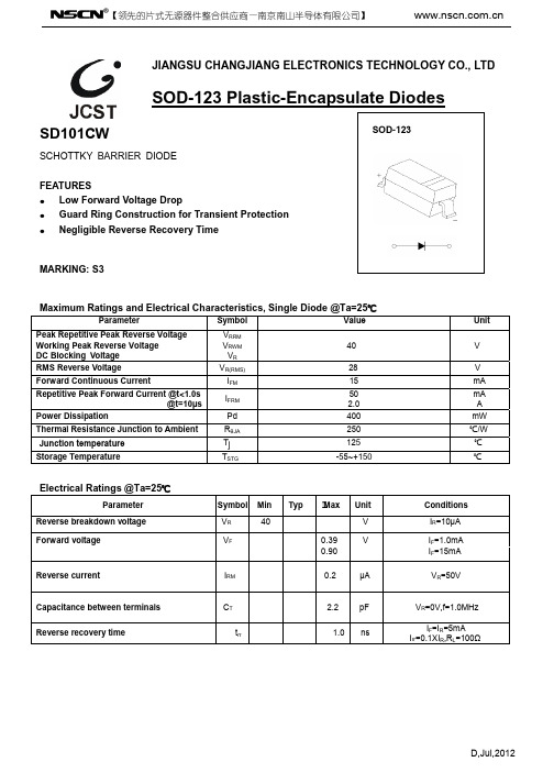
JIANGSU CHANGJIANG ELECTRONICS TECHNOLOGY CO., LTD
SOD-123 Plastic-Encapsulate Diodes
SD101CW
SCHOTTKY BARRIER DIODE
IFM
15
Repetitive Peak Forward Current @t<1.0s @t=10µsຫໍສະໝຸດ IFRM50 2.0
Power Dissipation
Pd
400
Thermal Resistance Junction to Ambient
RθJA
250
Junction temperature
Tj
Forward Characteristics
15
10
1
Ta=100℃
0.1
0.01
Ta=25℃
1E-3 0
100
200
300
400
500
FORWARD VOLTAGE VF (mV)
Capacitance Characteristics
3.6
Ta=25℃ f=1MHz
3.2
2.8
2.4
2.0
1.6
VR=50V
VR=0V,f=1.0MHz IF=IR=5mA
Irr=0.1XIR,RL=100Ω
D,Jul,2012
【领先的片式无源器件整合供应商—南京南山半导体有限公司】
Typical Characteristics
SD101CW
FORWARD CURRENT IF (mA)
奥德维特说明书

PDA 系列产品的设计、制造、检查、试验及特性都应遵照适合的最新版IEC 和中国GB 标准及国际单位SI 制。
GB/T13730《地区电网数据采集与监控系统通用技术条件》GB/50171-92《电气装置安装工作盘、柜及二次回路接线施工及验收规范》DL/T630《交流采样远动终端通用技术条件》DL/478-92《静态继电保护及安全自动装置通用技术条件》GB/50062-92《电力装置的继电保护和自动装置设计规范》GB/T50063-2008《电力装置的电测量仪表装置设计规范》DL/T587-1996《微机继电保护装置运行管理规程》GB/T13729-2002《远动终端通用技术条件》GB/14285-93《继电保护和安全自动装置技术规程》GB/T17626.12-1998《振荡波抗扰度试验》GB/T17626.11-2008《电压暂降、短时中断和电压变化抗扰度试验》GB/T17626.10-1998《阻尼振荡磁场抗扰度试验》GB/T17626.8-2006《工频磁场的抗扰度试验》GB/T17626.6-2008《射频场感应的传导骚扰抗扰度》GB/T17626.5-2008《浪涌(冲击)抗扰度试验》GB/T17626.4-2008《电快速瞬变脉冲群抗扰度试验》GB/T17626.2-2006《静电放电抗扰度试验》GB/T 14047-1993《量度继电器和保护装置》GB 3836.3-2000《爆炸性气体环境用电气设备 第 3 部 分:增安型"e"》JB/T 10613-2006《数字式电动机综合保护装置》GB/T13850-1998《交流电量转换为模拟量或数字信号的电测量变送器》JJG596-1999《电子式电能表检定规程》GB/T17215.321-2008《静止式有功电能表(1级和2级)》GB/T 22264-2008《安装式数字显示电测量仪表》产品标准Contents 目 录A -01综合电力监控仪PDA-120系列B -13 三相智能型电力仪表 PDA-103系列C -31单相智能型电力仪表 PDA-101系列D -51 智能型电动机保护控制器 PDA-110MRK F -66参考设计图附录产品业绩G -73GB/T17215.322-2008《》静止式有功电能表(0.2S 级和0.5S 级)E -58 低压电动机保护装置 ADVP-1451产品简介功能详表产品特点PDA -120系列综合电力监控仪是北京奥德威特电力科技股份有限公司按IEC 国际标准开发,与当今国际先进技术同步的网络化综合电力监控仪表。
TH2515 仪器说明书
Ver 2.1目录Ver 2.0 (2)第1章仪器简介与开箱安装 (8)1.1仪器简介 (8)1.2开箱检查 (8)1.3电源连接 (8)1.4保险丝 (8)1.5环境 (8)1.6使用测试夹具 (9)1.7预热 (9)1.8仪器的其它特性 (9)第2章前面板说明及入门操作 (10)2.1前面板说明 (10)2.2后面板说明 (11)2.3显示区域的定义 (12)2.4按键及其相应的显示页面 (13)2.4.1测量主菜单按键【DISP】 (13)2.4.2系统设置主菜单按键【SETUP】 (13)2.5基本操作 (13)2.6开机 (14)第3章基本操作 (15)3.1<测量显示>页面 (15)3.1.1测试功能 (15)3.1.2测试量程 (16)3.1.3测试速度 (17)3.1.4文件管理 (17)3.1.5其他工具 (17)3.2<比较显示>页面 (18)3.2.1文件管理 (19)3.2.2工具 (19)3.2.3比较 (19)3.2.4比较模式和上下限、百分比误差设置 (19)3.3<档显示>页面 (19)3.4<统计显示>页面 (21)3.4.1边界模式和其相应值的设定 (21)3.4.2统计状态 (21)3.4.3统计分析参数说明 (21)3.4.4工具 (22)3.4.5文件 (22)3.5<测量设置>页面 (22)3.6<TC/Δt设置>页面 (24)3.6.1温度校正(Temperature Correction 简称TC) (25)3.6.2温度转换(temperature conversion 简称t ) (25)3.6.3温度传感器的类型 (26)3.6.4参数设定 (27)3.6.5文件 (27)3.7<档设置>页面 (27)3.7.1文件 (29)3.7.2工具 (29)第4章系统设置和文件管理 (30)4.1系统设置 (30)4.1.1触摸音 (30)4.1.2语言 (30)4.1.3口令 (31)4.1.4总线模式 (31)4.1.5波特率 (32)4.1.6总线地址 (32)4.1.7EOC信号 (32)4.1.8Err.OUT信号 (33)4.1.9电源频率 (34)4.1.10时间和日期设定 (34)4.2<文件管理>功能页面 (34)4.2.1存储/调用功能简介 (34)4.2.2U盘上的文件夹/文件结构 (35)4.2.3DHCP (39)4.2.4IP地址 (40)4.2.5子网掩码 (40)4.2.6网关 (40)4.2.7首选DNS、备用DNS (40)第5章性能指标 (41)5.1测量功能 (41)5.1.1测量参数及符号 (41)5.1.2测量组合 (41)5.1.3等效方式 (41)5.1.4量程 (41)5.1.5触发 (41)5.1.6测试端方式 (41)5.1.7测量中的各种时间的开销 (41)5.1.8平均 (42)5.1.9显示的位数 (42)5.2测试信号 (42)5.2.1量程电流 (42)5.2.2开路输出电压 (42)5.2.3测量显示最大范围 (42)5.3测量准确度 (43)5.3.2温度测量的准确度(Pt500) (44)5.3.3温度测量的准确度(模拟输入) (45)5.3.4温度修正系数K (45)第6章远程控制 (46)6.1RS232C接口说明 (46)6.2GPIB接口说明(选购件) (47)6.2.1GPIB接口功能 (49)6.2.2GPIB 地址 (49)6.2.3GPIB总线功能 (49)6.2.4可编程仪器命令标准(SCPI) (50)6.3LAN远程控制系统 (50)6.3.1通过浏览器访问TH2515 (52)6.3.2通过上位机软件访问TH2515 (52)6.4USBTMC远程控制系统 (53)6.4.1系统配置 (53)6.4.2安装驱动 (53)6.5USBVCOM虚拟串口 (54)6.5.1系统配置 (54)6.5.2安装驱动 (54)第7章RS232命令参考 (55)7.1SCPI系统命令 (55)7.1.1DISPlay子系统命令集 (55)7.1.2FUNCtion 子系统命令集 (56)7.1.3APERture子系统命令集 (61)7.1.4TRIGer子系统命令集 (61)7.1.5FETCh?子系统命令集 (63)7.1.6TEMPerature子系统命令集 (64)7.1.7COMParator子系统命令集 (66)7.1.8BIN子系统命令集 (69)7.1.9STA Tistics子系统命令集 (73)7.1.10IO子系统命令集 (76)7.1.11MEMory子系统命令集 (77)7.1.12SYSTem 子系统命令集 (78)7.1.13SCPI公用命令 (81)7.2MODBUS系统命令 (83)7.2.1MODBUS协议说明 (84)7.2.2公用指令操作说明 (85)7.2.3DISP指令操作说明 (86)7.2.4FUNC指令操作说明 (86)7.2.5APER指令操作说明 (87)7.2.6TRIG指令操作说明 (87)7.2.7FETC指令操作说明 (88)7.2.8TEMP指令操作说明 (88)7.2.10BIN指令操作说明 (90)7.2.11STA T指令操作说明 (93)7.2.12IO指令操作说明 (94)7.2.13SYST指令操作说明 (94)第8章Handler接口使用说明及程序升级方法 (99)第9章包装及保修 (103)9.1标志 (103)9.2包装 (103)9.3运输 (103)9.4贮存 (103)9.5保修 (103)本说明书所描述的可能并非仪器所有内容,同惠公司有权对本产品的性能、功能、内部结构、外观、附件、包装物等进行改进和提高而不作另行说明!由此引起的说明书与仪器不一致的困惑,可通过封面的地址与我公司进行联系。
SDC212_规格书,PDF,电路图,方案

概述SDC212是一款低功耗霍尔开关。
应用于磁场检测,给出相应的数字输出。
在2.7V 时的典型功耗小于10uW ,因此非常适用于低耗电产品,可用于优先考虑功耗的电池供电系统,如折叠式移动电话,笔记本电脑等。
此产品具有精准的磁性开关切换点,而且其对于工艺差异和温度变化的灵敏度低。
应用⏹ 折叠、滑盖、旋屏式移动电话⏹笔记本电脑、数码相机等特点⏹ 低功耗⏹ 工作电压2.4V 至4.5V⏹斩波放大器设计,对因工艺、工作温度和机械应力产生的噪声和失调敏感度低⏹ 不区分磁场极性,N极和S 极均可使用 ⏹ 数字输出 ⏹ 采用CMOS 工艺 ⏹SOT-23-3、TO-92S 封装管脚描述231S D C 212图1管脚排布图编号SOT23-3 TO-92S名称功能 1 1 VDD 电源 3 2 VSS 地 2 3Q输出表1管脚描述功能框图图2功能框图订购信息封装 温度范围标识号 打印Pb-free Halogen-free Pb-freeHalogen-free包装形式TO-92SSDC212ZS-E1SDC212ZS-G1212 212 袋装SOT-23-3-40~85℃SDC212J-E1 SDC212J-G12XX (XX代表D/C)2XX (XX代表D/C)编带极限参数参 数条 件 数 值 单 位环境工作温度范围 - -40~85 ℃ 储存温度范围 - -40~150 ℃直流供应电压 - 2.4~5.0 V 供应电流 - -1~2.5 mA 磁感应强度-无限制 ℃ PIN 脚焊接温度 10秒<260℃表2最大额定值推荐工作条件参 数符 号 条 件 下 限 典 型 上 限 单 位供应电压范围 VDD - 2.4 2.7 4.5 V 输出电压范围 Vout - -0.3 2.7 4.5 V 环境温度范围Temp - -40 25 85 ℃表3推荐额定值电气参数(若无特别指明,VDD=2.7V,Ta=25℃)参 数符 号 条 件 下 限 典 型 上 限 单 位静态参数平均供应电流 Idd VDD=2.7V -3 20uA 工作电流 Ion VDD=2.7V - 1.1 - mA 待机电流 Ist VDD=2.7V - 2.5 - uA 输出饱和电压 Vsat Isat=2mA - 0.1 - V 输出漏电流 Ileak Vout=4.5V - 0.01 - uA 工作时间 Ton VDD=2.7V - 60 - us 待机时间Toff VDD=2.7V -75-ms磁场特性工作点 |BOP| -- 30 35G 释放点 |BRP| - 15 20 - G 磁滞宽度BHY - - 10 -G表3电磁特性特性曲线图3平均电流相对于环境温度变化曲线(VDD=2.7V)图4平均电流相对于电源电压变化曲线(Temp=25℃)磁场检测示意图图5磁场特性图工作原理 启动复位偏置电路当电源开启时,启动复位电路立即重置数字电路以在启动后获得正确的操作。
家电维修_常用三极管_2SD1212_电路资料

SANYO Electric Co.,Ltd. Semiconductor Bussiness HeadquatersTOKYO OFFICE Tokyo Bldg., 1-10, 1 Chome, Ueno, Taito-ku, TOKYO, 110-8534 JAPANPNP/NPN Epitaxial Planar Silicon TransistorsOrdering number:990Cre t e m a r a P l o b m y S sn o i t i d n o C sg n i t a R t i n U e g a t l o V e s a B -o t -r o t c e l l o C V O B C 06)–(V e g a t l o V r e t t i m E -o t -r o t c e l l o C V O E C 03)–(V e g a t l o V e s a B -o t -r e t t i m E V O B E 6)–(V t n e r r u C r o t c e l l o C I C 21)–(A )e s l u P (t n e r r u C r o t c e l l o C I P C 02)–(A n o i t a p i s s i D r o t c e l l o C P C57.1W 53We r u t a r e p m e T n o i t c n u J j T 051er u t a r e p m e T e g a r o t S gt s T 051+o t 55–( ) : 2SB903SpecificationsAbsolute Maximum Ratings at Ta = 25˚CPackage Dimensionsunit:mm 2010C[2SB903/2SD1212]Applications· Suitable for relay drivers, high-speed inverters,converters, and other general large-current switching applications.Features· Low collector-to-emitter saturation voltage : V CE(sat)=(–)0.5V (PNP), 0.4V (NPN) max. ·Large current capacity.˚C ˚CElectrical Characteristics at Ta = 25˚CJEDEC : TO-220AB 1 : Base EIAJ : SC-462 : Collector3 : EmitterTc=25˚Cre t e m a r a P l o b m y S sn o i t i d n o C sg n i t a R t i n U ni m py t x a m t n e r r u C f f o t u C r o t c e l l o C I O B C V B C I ,V 04)–(=E 0=1.0)–(A m t n e r r u C f f o t u C r e t t i m E I O B E V B E I ,V 4)–(=C 0=1.0)–(Am n i a G t n e r r u C C D h E F 1V E C I ,V 2)–(=C A 1)–(=*07*082h E F 2V E C I ,V 2)–(=C A 6)–(=03tc ud o r P h t d i w d n a B -n i a G f TV E C I ,V 5)–(=C A1)–(=021zH M * : The 2SB903/2SD1212 are graded as follows by h FE at 1A :41Q7002R01082S41Switching Time Test CircuitUnit (resistance : Ω, capacitance : F)re t e m a r a P l o b m y S sn o i t i d n o C sg n i t a R t i n U ni m py t x a m e g a t l o V n o i t a r u t a S r e t t i m E -o t -r o t c e l l o C V )t a s (E C I C I ,A 5)–(=B A52.0)–(=)5.0–(V 4.0V e g a t l o V n w o d k a e r B e s a B -o t -r o t c e l l o C V O B C )R B (I C I ,A m 1)–(=E 0=06)–(V e g a t l o V n w o d k a e r B r e t t i m E -o t -r o t c e l l o C V O E C )R B (I C R ,A m 1)–(=E B =∞03)–(V e g a t l o V n w o d k a e r B e s a B -o t -r e t t i m E V OB E )R B (I E I ,A m 1)–(=C 0=6)–(V e m i T N O -n r u T t no ti u c r i C t s e T d e i f i c e p s e e S )1.0(s µ2.0s µe m i T e g a r o t S t g t s t i u c r i C t s e T d e i f i c e p s e e S )3.0(s µ5.0s µem i T l l a F t fti u c r i C t s e T d e i f i c e p s e e S 30.0sµSpecifications of any and all SANYO products described or contained herein stipulate the performance, characteristics,and functions of the described products in the independent state,of the performance,characteristics,and functions of the described products as mounted in the customer’s products or equipment. To verify symptoms and states that cannot be evaluated in an independent device, the customer should always evaluate and test devices mounted in the customer’s products or equipment. SANYO Electric Co.,Ltd. strives to supply high-quality high-reliability products. However, semiconductor products fail with some probability. It is possible that these probabilistic failures could give rise to accidents or events that could endanger human lives,。
ELX1216 10 x 32 mm高功能断忙电容器说明书
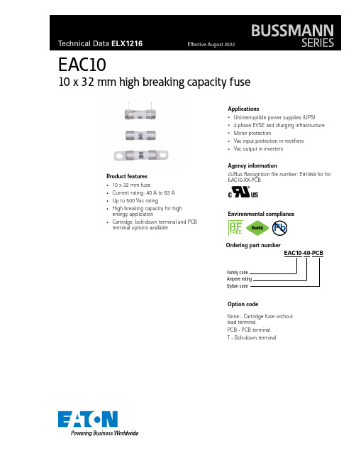
EAC1010 x 32 mm high breaking capacity fuseProduct features• 10 x 32 mm fuse• Current rating: 40 A to 63 A• Up to 500 Vac rating• High breaking capacity for high energy application• Cartridge, bolt-down terminal and PCB terminal options available Applications• Uninterruptible power supplies (UPS)• 3-phase EVSE and charging infrastructure • Motor protection• Vac input protection in rectifiers• Vac output in invertersAgency informationcURus Recognition file number: E91958 for forEAC10-XX-PCBEnvironmental complianceHALOGENHFFREEEAC10-40-PCBFamily codeAmpere ratingOption codeOrdering part numberPbOption codeNone - Cartridge fuse without lead terminalPCB - PCB terminalT - Bolt-down terminal2Technical Data ELX1216Effective August 2022EAC1010 x 32 mm high breaking capacity fuse/electronicsElectrical characteristicsCurrent and time characteristics1.0 In 1 hour minimum2.0 In120 seconds maximumProduct specificationsTypical cold resistance 1Power Loss at 1.0 In Part number Rated voltage Rated current Breaking capacity(mOhms)(W)EAC10-40500 Vac 250 Vac 40 A 2000 A @ 500 Vac 10000 A @ 250 Vac 1.71 4.7EAC10-50500 Vac 250 Vac 50 A 2000 A @ 500 Vac 10000 A @ 250 Vac 1.33 5.7EAC10-63500 Vac 250 Vac63 A2000 A @ 500 Vac 10000 A @ 250 Vac1.057.51. DC Cold Resistance measured at <10% of rated current in the ambient temperature of +25 °CDimensions- mmDrawing not to scalePCB terminal versionCartridge versionBolt versionNote: recommend tightening torque is 3.5-4 Nm for M5 screwRecommended PCB layoutPart marking(Example: EAC10-63)3Technical Data ELX1216Effective August 2022EAC1010 x 32 mm high breaking capacity fuse /electronics Packaging information - mmGeneral specificationsMechanical vibration: MIL-STD-202, Method 201, For EAC10-XX; EAC10-XX-PCB and EAC10-XX-TThermal shock: MIL-STD-202, Method 107,Test Condition B (5 cycles -65°C to 125°C), For EAC10-XX; EAC10-XX-PCB and EAC10-XX-T Humidity: MIL-STD-202, Method 103, Test Condition A: 95% RH and 40 °C for 240 hours, For EAC10-XX; EAC10-XX-PCB and EAC10-XX-T Salt spray: MIL-STD-202, Method 101 Test condition B, For EAC10-XX; EAC10-XX-PCB and EAC10-XX-T Thermal shock resistance: JASO D622 6.3.6, For EAC10-XX-PCB and EAC10-XX-T onlyTransient current intermittent cycle durability: JASO D622 6.3.2, For EAC10-XX-PCB and EAC10-XX-T only Heat resistance to soldering: MIL-STD-202 Method 210, For EAC10-XX-PCB only Terminal strength: MIL-STD-202, Method 211, Test Condition A, For EAC10-XX-T only Lead solderability: MIL-STD-202, Method 208, For EAC10-XX-PCB only45 pcs in a plastic tray, 10 trays (450 pcs) in a carton4Technical Data ELX1216Effective August 2022EAC1010 x 32 mm high breaking capacity fuse/electronicsT emperature derating curveCurrent vs. time curve D e r a t i n g f a c t o rT emperature (°C)Current (A)T i m e (s e c o n d s)I 2T and time curveTime (S)I 2t (A 2s )5Technical Data ELX1216Effective August 2022EAC1010 x 32 mm high breaking capacity fuse /electronics I 2t and current curveCurrent (A)I 2t (A 2s)EatonElectronics Division 1000 Eaton Boulevard Cleveland, OH 44122United States/electronics© 2022 EatonAll Rights Reserved Printed in USAPublication No. ELX1216 BU-ELX22076August 2022EAC1010 x 32 mm high breaking capacity fuseTechnical Data ELX1216Effective August 2022Life Support Policy: Eaton does not authorize the use of any of its products for use in life support devices or systems without the express writtenapproval of an officer of the Company. Life support systems are devices which support or sustain life, and whose failure to perform, when properly used in accordance with instructions for use provided in the labeling, can be reasonably expected to result in significant injury to the user.Eaton reserves the right, without notice, to change design or construction of any products and to discontinue or limit distribution of any products. Eaton also reserves the right to change or update, without notice, any technical information contained in this bulletin.T e m p e r a t u r eTimeT T T T Wave solder profile--PCB version onlyReference EN 61760-1:2006Profile featureStandard SnPb solderLead (Pb) free solderPreheat • Temperature min. (T smin )100 °C 100 °C • Temperature typ. (T styp )120 °C 120 °C • Temperature max. (T smax )130 °C 130 °C • Time (T smin to T smax ) (t s )70 seconds 70 seconds D preheat to max Temperature150 °C max.150 °C max.Peak temperature (T P )*235 °C – 260 °C 250 °C – 260 °C Time at peak temperature (t p )10 seconds max5 seconds max each wave 10 seconds max5 seconds max each wave Ramp-down rate~ 2 K/s min ~3.5 K/s typ ~5 K/s max ~ 2 K/s min ~3.5 K/s typ~5 K/s max Time 25 °C to 25 °C4 minutes4 minutesManual solder+350 °C (4-5 seconds by soldering iron), generally manual/hand soldering is not recommended.Eaton is a registered trademark.All other trademarks are property of their respective owners.Follow us on social media to get the latest product and support information.。
2SD1615中文资料
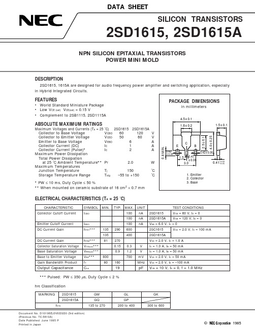
Document No. D10198EJ3V0DSD0 (3rd edition) (Previous No. TC-5810A)Date Published June 1995 P Printed in Japan ©198522SD1615, 2SD1615ATYPICAL CHARACTERISTICS (T A = 25 ˚C)T A – Ambient Temperature – ˚C4080120160200P T – T o t a l P o w e r D i s s i p a ti o n – WTOTAL POWER DISSIPATION vs.AMBIENT TEMPERATURECOLLECTOR CURRENT vs.BASE TO EMITTER VOLTAGEV CE – Collector to Emitter Voltage – VI C – C o l l e c t o r C u r r e n t – m AI C – Collector Current – ADC CURRENT GAIN vs.COLLECTOR CURRENTh E F – D C C u r r e n t G a i nCOLLECTOR CURRENT vs.COLLECTOR TO EMITTER VOLTAGEV CE(sat) – Collector Saturation Voltage – V I C – C o l l e c t o r C u r r e n t – A0.010.020.050.10.20.512510I C – Collector Current – ACOLLECTOR AND BASE SATURATION VOLTAGE vs. COLLECTOR CURRENTV C E (s a t ) – C o ll e c t o r S a t u r a t i o n V o l t a g e – V V B E (s a t ) – B a s e S a t u r a t i o n V o l t a g e – VSAFE OPERATING AREA(TRANSIENT THERMAL RESISTANCE METHOD)5210.50.20.10.050.020.01125102050100V CE – Collector to Emitter Voltage – V I C – C o l l e c t o r C u r r e n t – A3GAIN BANDWIDTH PRODUCT vs.EMITTER CURRENTf T – G a i n B a n d w i d t h P r o d u c t – M H ZI C– Collector Current – AOUTPUT CAPCITANCE vs.COLLECTOR TO BASE VOLTAGEC o b – O u t p u t C a p a c i t a n c e – p FV CB – Collector to Base Voltage – VI C – Collector Current – ASWITCHING TIME vs.COLLECTOR CURRENTt – S w i t c h i n g T i m e– sµREFERENCE[MEMO]No part of this document may be copied or reproduced in any form or by any means without the prior written consent of NEC Corporation. NEC Corporation assumes no responsibility for any errors which may appear in this document.NEC Corporation does not assume any liability for infringement of patents, copyrights or other intellectual property rights of third parties by or arising from use of a device described herein or any other liability arising from use of such device. No license, either express, implied or otherwise, is granted under any patents, copyrights or other intellectual property rights of NEC Corporation or others.While NEC Corporation has been making continuous effort to enhance the reliability of its semiconductor devices, the possibility of defects cannot be eliminated entirely. To minimize risks of damage or injury to persons or property arising from a defect in an NEC semiconductor device, customer must incorporate sufficient safety measures in its design, such as redundancy, fire-containment, and anti-failure features.NEC devices are classified into the following three quality grades:“Standard“, “Special“, and “Specific“. The Specific quality grade applies only to devices developed based ona customer designated “quality assurance program“ for a specific application. The recommended applicationsof a device depend on its quality grade, as indicated below. Customers must check the quality grade of each device before using it in a particular application.Standard:Computers, office equipment, communications equipment, test and measurement equipment, audio and visual equipment, home electronic appliances, machine tools, personal electronicequipment and industrial robotsSpecial:Transportation equipment (automobiles, trains, ships, etc.), traffic control systems, anti-disaster systems, anti-crime systems, safety equipment and medical equipment (not specifically designedfor life support)Specific:Aircrafts, aerospace equipment, submersible repeaters, nuclear reactor control systems, life support systems or medical equipment for life support, etc.The quality grade of NEC devices in “Standard“ unless otherwise specified in NEC's Data Sheets or Data Books.If customers intend to use NEC devices for applications other than those specified for Standard quality grade, they should contact NEC Sales Representative in advance.Anti-radioactive design is not implemented in this product.M4 94.11。
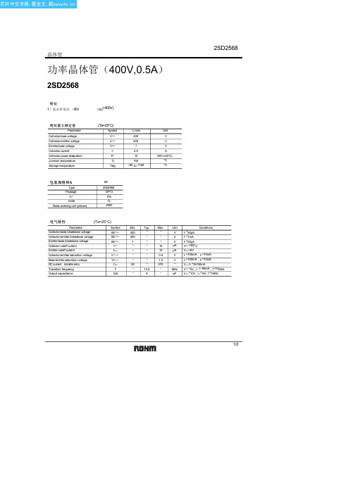
2SD2568中文资料(rohm)中文数据手册「EasyDatasheet - 矽搜」
0.5 (A)
1
0.5 (A)
1
0.02 BASE SATURATION VOLTAGE : V 0.01 0.001 0.002 0.005 0.01 0.02 0.05 0.1 0.2 COLLECTOR CURRENT : I
C
0.5 (A)
1
COLLECTOR CURRENT : I
图4 DC电流增益 - 集电极电流(
1/2
芯片中文手册,看全文,戳
2SD2568
晶体管电气特Biblioteka 曲线200 (mA) 160
C
Ta=25 C
mA 3.0m A 2.5m A 2.0m A 1.5m A
1 (A)
C
V CE =3V
FE
1000 500 200 100
Ta=25 C
0.5 0.2 0.1 0.05
25°C
FE
2SD2568 CPT3 PQ TL 2500
电气特性
Parameter Collector-base breakdown voltage Collector-emitter breakdown voltage Emitter-base breakdown voltage Collector cutoff current Emitter cutoff current Collector-emitter saturation voltage Base-emitter saturation voltage DC current transfer ratio Transition frequency Output capacitance
(V) 2
BE(sat)
200 100 50 20
QEC122,QEC123, 规格书,Datasheet 资料
QEC121, QEC122, QEC123 — Plastic Infrared Light Emitting Diode
Absolute Maximum Ratings (TA = 25°C unless otherwise specified)
Stresses exceeding the absolute maximum ratings may damage the device. The device may not function or be operable above the recommended operating conditions and stressing the parts to these levels is not recommended. In addition, extended exposure to stresses above the recommended operating conditions may affect device reliability. The absolute maximum ratings are stress ratings only.
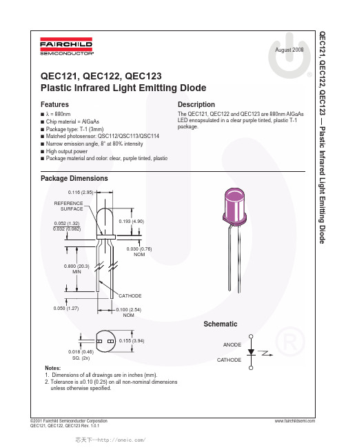
Figure 7. Radiation Diagram
100° 90° 80°
110°
70°
120°
60°
130°
50°
140°
40°
150°
30°
160°
20°
170°
10°
180°
0°
1.0 0.8 0.6 0.4 0.2 0.0 0.2 0.4 0.6 0.8 1.0
IC (ON) – NORMALIZED COLLECTOR CURRENT
QEC121, QEC122, QEC123 Rev. 1.0.1
2SD2012(F,M);中文规格书,Datasheet资料
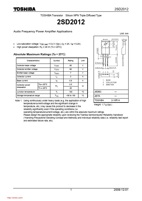
TOSHIBA Transistor Silicon NPN Triple Diffused Type2SD2012Audio Frequency Power Amplifier Applications• Low saturation voltage: V CE (sat) = 0.4 V (typ.) (I C = 2A / I B = 0.2A) • High power dissipation: P C = 25 W (Tc = 25°C)Absolute Maximum Ratings (Ta = 25°C)Characteristics Symbol Rating UnitCollector-base voltage V CBO 60 V Collector-emitter voltage V CEO 60 V Emitter-base voltage V EBO 7 V Collector current I C 3 A Base current I B 0.5 A Ta = 25°C 2.0 Collector powerdissipationTc = 25°CP C25WJunction temperature T j 150 °C Storage temperature rangeT stg−55 to 150°CNote 1: Using continuously under heavy loads (e.g. the application of hightemperature/current/voltage and the significant change in temperature, etc.) may cause this product to decrease in the reliability significantly even if the operating conditions (i.e.operating temperature/current/voltage, etc.) are within the absolute maximum ratings.Please design the appropriate reliability upon reviewing the Toshiba Semiconductor Reliability Handbook(“Handling Precautions”/Derating Concept and Methods) and individual reliability data (i.e. reliability test report and estimated failure rate, etc).Unit: mmJEDEC ― JEITA―TOSHIBA 2-10R1A Weight: 1.7 g (typ.)Electrical Characteristics (Ta = 25°C)Typ.Max UnitCondition Min Characteristics Symbol TestCollector cut-off current I CBO V CB = 60 V, I E = 0 ―― 100μA Emitter cut-off current I EBO V EB = 7 V, I C = 0 ―― 100μA Collector-emitter breakdown voltage V (BR) CEO I C = 50 mA, I B = 0 60 ―― Vh FE (1)V CE = 5 V, I C = 0.5 A 100 ― 320DC current gainh FE (2)V CE = 5 V, I C = 2 A 20 ――Collector-emitter saturation voltage V CE (sat)I C = 2 A, I B = 0.2 A ― 0.4 1.0 V Base-emitter voltage V BE V CE = 5 V, I C = 0.5 A ― 0.75 1.0 V Transition frequency f T V CE = 5 V, I C = 0.5 A ― 3 ― MHz Collector output capacitance C ob V CB = 10 V, I E = 0, f = 1 MHz ― 35 ― pF MarkingD2012Note 2: A line under a Lot No. identifies the indication of product Labels.Not underlined: [[Pb]]/INCLUDES > MCVUnderlined: [[G]]/RoHS COMPATIBLE or [[G]]/RoHS [[Pb]]Please contact your TOSHIBA sales representative for details as to environmental matters such as the RoHScompatibility of Product. The RoHS is the Directive 2002/95/EC of the European Parliament and of the Council of 27 January 2003 on the restriction of the use of certain hazardous substances in electrical and electronic equipment.Collector-emitter voltage V CE (V)I C – V CECo l le c t o r c u r r e n tI C (A )Collector current I C (A)h FE – ICD C c u r r e n t g a in h F ECollector current I C (A)V CE (sat) – I CC o l l e c t o r -e m i t t e r s a t u r a t io nv o l t a g e V C E (sa t ) (V )Base-emitter voltage V BE (V)I C – V BEC ol lect o rc u rr en tI C(A )Ambient temperature Ta (°C)P C – TaC o l l e c t o r p o w e r d i s s i p a t i o n P C (W )Collector-emitter voltage V CE (V)Safe Operating AreaC o l l e c t o r c u r r e n t I C (A )Pulse width t w (s)r th – t wT r a n s i e n t t h e r m a l r e s i s t a n c e r t h (°C /W )1 10 1000.10.010.001RESTRICTIONS ON PRODUCT USE•Toshiba Corporation, and its subsidiaries and affiliates (collectively “TOSHIBA”), reserve the right to make changes to the information in this document, and related hardware, software and systems (collectively “Product”) without notice.•This document and any information herein may not be reproduced without prior written permission from TOSHIBA. Even with TOSHIBA’s written permission, reproduction is permissible only if reproduction is without alteration/omission.•Though TOSHIBA works continually to improve Product’s quality and reliability, Product can malfunction or fail. Customers are responsible for complying with safety standards and for providing adequate designs and safeguards for their hardware, software and systems which minimize risk and avoid situations in which a malfunction or failure of Product could cause loss of human life, bodily injury or damage to property, including data loss or corruption. Before customers use the Product, create designs including the Product, or incorporate the Product into their own applications, customers must also refer to and comply with (a) the latest versions of all relevant TOSHIBA information, including without limitation, this document, the specifications, the data sheets and application notes for Product and the precautions and conditions set forth in the “TOSHIBA Semiconductor Reliability Handbook” and (b) theinstructions for the application with which the Product will be used with or for. Customers are solely responsible for all aspects of their own product design or applications, including but not limited to (a) determining the appropriateness of the use of this Product in such design or applications; (b) evaluating and determining the applicability of any information contained in this document, or in charts, diagrams, programs, algorithms, sample application circuits, or any other referenced documents; and (c) validating all operating parameters for such designs and applications. TOSHIBA ASSUMES NO LIABILITY FOR CUSTOMERS’ PRODUCT DESIGN OR APPLICATIONS.•Product is intended for use in general electronics applications (e.g., computers, personal equipment, office equipment, measuring equipment, industrial robots and home electronics appliances) or for specific applications as expressly stated in this document.Product is neither intended nor warranted for use in equipment or systems that require extraordinarily high levels of quality and/or reliability and/or a malfunction or failure of which may cause loss of human life, bodily injury, serious property damage or serious public impact (“Unintended Use”). Unintended Use includes, without limitation, equipment used in nuclear facilities, equipment used in the aerospace industry, medical equipment, equipment used for automobiles, trains, ships and other transportation, traffic signaling equipment, equipment used to control combustions or explosions, safety devices, elevators and escalators, devices related to electric power, and equipment used in finance-related fields. Do not use Product for Unintended Use unless specifically permitted in this document.•Do not disassemble, analyze, reverse-engineer, alter, modify, translate or copy Product, whether in whole or in part.•Product shall not be used for or incorporated into any products or systems whose manufacture, use, or sale is prohibited under any applicable laws or regulations.•The information contained herein is presented only as guidance for Product use. No responsibility is assumed by TOSHIBA for any infringement of patents or any other intellectual property rights of third parties that may result from the use of Product. No license to any intellectual property right is granted by this document, whether express or implied, by estoppel or otherwise.•ABSENT A WRITTEN SIGNED AGREEMENT, EXCEPT AS PROVIDED IN THE RELEVANT TERMS AND CONDITIONS OF SALE FOR PRODUCT, AND TO THE MAXIMUM EXTENT ALLOWABLE BY LAW, TOSHIBA (1) ASSUMES NO LIABILITYWHATSOEVER, INCLUDING WITHOUT LIMITATION, INDIRECT, CONSEQUENTIAL, SPECIAL, OR INCIDENTAL DAMAGES OR LOSS, INCLUDING WITHOUT LIMITATION, LOSS OF PROFITS, LOSS OF OPPORTUNITIES, BUSINESS INTERRUPTION AND LOSS OF DATA, AND (2) DISCLAIMS ANY AND ALL EXPRESS OR IMPLIED WARRANTIES AND CONDITIONS RELATED TO SALE, USE OF PRODUCT, OR INFORMATION, INCLUDING WARRANTIES OR CONDITIONS OF MERCHANTABILITY, FITNESS FOR A PARTICULAR PURPOSE, ACCURACY OF INFORMATION, OR NONINFRINGEMENT.•Do not use or otherwise make available Product or related software or technology for any military purposes, including without limitation, for the design, development, use, stockpiling or manufacturing of nuclear, chemical, or biological weapons or missile technology products (mass destruction weapons). Product and related software and technology may be controlled under the Japanese Foreign Exchange and Foreign Trade Law and the U.S. Export Administration Regulations. Export and re-export of Product or related software or technology are strictly prohibited except in compliance with all applicable export laws and regulations. •Please contact your TOSHIBA sales representative for details as to environmental matters such as the RoHS compatibility of Product.Please use Product in compliance with all applicable laws and regulations that regulate the inclusion or use of controlled substances, including without limitation, the EU RoHS Directive. TOSHIBA assumes no liability for damages or losses occurring as a result of noncompliance with applicable laws and regulations.分销商库存信息: TOSHIBA2SD2012(F,M)。
ht1621中文资料
SD0432 中集成了一个简单的声音发生器,此发声器可输出一对不同的驱动信号至 BZ 和 BZ 以产生单音,执 行 TONE 4K 与 TONE 2K 命令,可选择两个不现的音频输出,即 4KHZ 与 2KHZ 这两个频率,TONE ON 及 TONE OFF 命令可打开或关闭语音输出,语音输出 BZ 和 BZ,是一对不同的带驱动蜂鸣器。当系统关闭或语音输出被禁止时, BZ 及 BZ 将处于低电平状态。
命令 LCD OFF 是通过关闭 LCD 偏压发生器来关闭 LCD 显示器。反之,LCD ON 则启动 LCD 显示。BIAS COM 是与
LCD 屏面相关命令。使用 LCD 相关命令,SD0432 可与绝大多数类型的 LCD 屏面兼容。
3. 6 命令格式
SD0432 可由 S/W 设置来配置。有两种命令模式分别用来配置 SD0432 和传送 LCD 显示数据。配置 SD0432 的命
令模式(普通模式)识别码为 100,此命令模式由系统配置命令、LCD 配置命令、音频选择命令、定时器/看门狗
定时器设置命令及操作命令组成。另一方面,数据模式包括 READ、WRITE 及 READ-MODIFY-WRITE 操作。下表为数
据模式及命令模式识别码:
com 操
作
. READ
s WRITE
le RAM 中的数据由 READ、WRITE 以及 READ-MODIFY-WRITE 指令进行存取,下图为由 RAM 控制 LCD 的映象图。
e SEG
COM
COM3
COM2
COM1
COM0
六位地址(A5,A4…A0)
. SEG0
0
ww SEG1
1
w SEG2
东殊半导体DS202线缆电子标签(PD E-Marked)芯片数据手册说明书
东殊半导体DS202线缆电子标签(PD E-Marked)芯片数据手册第4.0版Copy right © 2020 by DongShu Semiconductor(Shen Zhen) Co., Ltd., All rights reserved2022-10-10深圳龙华电话:136****2295网址:邮箱:**********************目录1.适用范围 (2)2.PD Emark功能简述 (2)3.典型电路 (3)4.电气特征 (4)5.工作范围 (4)6.PD Emarked数据 (5)7.关于认证 (5)1.适用范围根据USB IF,凡是USB3.0及以上线缆(USB3.1,USB3.2,USB4.0),或者是电源电流超过3A的USB2.0的线缆,均需要PD emark功能,那么具有PD Emark 功能的芯片DS202将能满足这方面的要求,当然你也可以使用东殊半导体的另一款DS201芯片,它的功能更为强大。
2.PD Emark功能简述根据USBIF的标准,PD Emark原理如下框图所示:其中Source指的是电源(比如手机充电器或笔记本电脑的电源),而Sink为需要电源的设备(比如手机或笔记本电脑),当Source给Sink供电时,需要通过PD线缆,而这根线缆两端都是TYPE-C结构,因为只有TYPE-C才有CC1和CC2两根连线,具体Source和Sink将利用CC1和CC2中的一根相互进行通讯(图中CC线),另一根线会对线缆中PD Emark功能模块进行供电(图中Vconn 线);Source会根据Sink的请求提供不同的电压,以及对电流进行限流控制,根据最新的PD协议,最高电压可以达到48V,最大电流可以达到5A。
但是不是所有的线缆能够承受最高48V的电压或最大5A的电流,这就是嵌在线缆中PD Emark芯片存在的意义,PD Emark芯片会告诉Source或Sink线缆的基本情况:可承受的最高电压和最大电流,以及线缆长度,制造商等其它信息。
EC12中文资料(Schurter)中文数据手册「EasyDatasheet - 矽搜」
EC12 EF12
芯片中文手册,看全文,戳
线集
CN电源线符合IEC设备接口C19,V型锁,直
C19
GB 2099
70° C
描述
- Power Cord, Protection class I, Pin temperature 70 °C, - 与V型锁联锁系统
技术数据
等级IEC
介电强度
允许工作温度.
变种
Connector
cable
Type V-Lock Cord Type
Color
C19 l
RVV 300/500 black 3x1.5
Length [m]
inlets Type
2.0
China
Country Standard CN GB 2099
Conductor cross section
3 x 1.5 mm²
verriegelt祖
Appliance InletOverview complete IEC Appliance Inlet C20, Screw-on Mounting, Rear Side, PCB Terminal IEC Appliance Inlet C20, Screw-on Mounting, Front Side, Solder, Quick-connect or Screw Terminal IEC Appliance Inlet C20, Snap-in Mounting, Front Side, Solder, Quick-connect or Screw Terminal IEC Appliance Inlet C20, Screw-on Mounting, Front Side, Solder or Quick-connect Terminal Appliance Inletfurther typestoVAC19KS
2SD1640规格书

104
Collector to emitter voltage VCE (V)
Time t (s)
2
Request for your special attention and precautions in using the technical information and semiconductors described in this material
3 25˚C 1 TC=100˚C –25˚C 0.3
0.1
0.5
30µA
0.03
0 0 2 4 6 8 10
0.01 0.01
0.03
0.1
0.3
1
3
Ambient temperature Ta (˚C)
Collector to emitter voltage VCE (V)
Collector current IC (A)
V
MHz
R
S
4 000 to 10 000 8 000 to 20 000 16 000 to 40 000
1
2SD1640
PC T a
1.6 3.0 Without heat sink 1.4 2.5 TC=25˚C IB=180µA
Power Transistors
IC VCE
Collector to emitter saturation voltage VCE(sat) (V)
Power Transistors
2SD1640
Silicon NPN epitaxial planar type darlington
Unit: mm
For low-frequency output amplification
ER1603FCT中文资料(Won-Top Electronics)中文数据手册「EasyDatasheet - 矽搜」

标识信息
WTE
ER160xFCT WTE =制造商标志 ER160xFCT =设备号 x = 0,1,1A,2,3,4或6个 极性 =对人体标示
封装信息
BULK
管尺寸 长×宽×高(mm) 数量 内箱尺寸 长×宽×高(mm) 数量 外箱尺寸 长×宽×高(mm) 数量 约.总重量
(PCS) 50
(PCS) 2,000
6-32六角头螺丝
平焊盘圈
锥形焊盘圈应该用于正确力施加到所述设 备.螺钉不应收紧与任何类型空气被迫扭 矩或器材可能导致裂纹器件封装.
整流器 散热器 锥形焊盘圈
导热硅脂或接口散热焊盘一层将是散热相当 有帮助.
6-32六角螺母
ER1600FCT – ER1606FCT
3 of 4
芯片中文手册,看全文,戳
芯片中文手册,看全文,戳
ER1600FCT – ER1606FCT
16A玻璃钝化双超快速整流器 特征
玻璃钝化模具结构 超快速切换 低正向压降 低反向漏电流 高浪涌电流能力 塑料材料具有UL可燃性 分类94V-O
Pb
B C G
PIN1 2 3
A
D
机械数据
案例:ITO-220,全模制塑料 终端:每焊镀信息 MIL-STD-202,方法208 极性:见图 重量:2.24克(约) 安装位置:任意 安装扭矩:11.5厘米千克(10磅)最大. 无铅:对于符合 RoHS /无铅版本 , 新增 "-LF"后缀型号 ,见第 4页
循环次数在60Hz 图. 3最大不重复浪涌电流
10 10 100 0.1 1.0 VR,反向电压(V) 图. 4典型结电容
t +0.5A
10
100
- 1、下载文档前请自行甄别文档内容的完整性,平台不提供额外的编辑、内容补充、找答案等附加服务。
- 2、"仅部分预览"的文档,不可在线预览部分如存在完整性等问题,可反馈申请退款(可完整预览的文档不适用该条件!)。
- 3、如文档侵犯您的权益,请联系客服反馈,我们会尽快为您处理(人工客服工作时间:9:00-18:30)。
TOSHIBA Transistor Silicon NPN Epitaxial Type (PCT Process) (Darlington)2SD1223Switching ApplicationsHammer Drive, Pulse Motor Drive Applications Power Amplifier Applications• High DC current gain: h FE = 2000 (min) (V CE = 2 V, I C = 1 A) • Low saturation voltage: V CE (sat) = 1.5 V (max) (I C = 3 A) • Complementary to 2SB908.Absolute Maximum Ratings (Ta = 25°C)Characteristics Symbol Rating UnitCollector-base voltage V CBO 100 V Collector-emitter voltage V CEO 80 V Emitter-base voltage V EBO 5 V Collector current I C 4A Base current IB 0.4 A Ta = 25°C 1.0 Collector powerdissipationTc = 25°CP C15WJunction temperature T j 150 °C Storage temperature rangeT stg−55 to 150°CNote: Using continuously under heavy loads (e.g. the application of hightemperature/current/voltage and the significant change in temperature, etc.) may cause this product to decrease in the reliability significantly even if the operating conditions (i.e. operating temperature/current/voltage, etc.) are within the absolute maximum ratings.Please design the appropriate reliability upon reviewing the Toshiba Semiconductor Reliability Handbook (“Handling Precautions”/”Derating Concept and Methods”) and individual reliability data (i.e. reliability test report and estimated failure rate, etc).Equivalent CircuitUnit: mmJEDEC― JEITA―TOSHIBA 2-7J1A Weight: 0.36 g (typ.)Electrical Characteristics (Ta = 25°C)MarkingNote 1: A line under a Lot No. identifies the indication of product Labels.Not underlined: [[Pb]]/INCLUDES > MCVUnderlined: [[G]]/RoHS COMPATIBLE or [[G]]/RoHS [[Pb]]Please contact your TOSHIBA sales representative for details as to environmental matters such as theRoHS compatibility of Product. The RoHS is the Directive 2002/95/EC of the European Parliament andof the Council of 27 January 2003 on the restriction of the use of certain hazardous substances inelectrical and electronic equipment.I C– V CEI C – V CEI C – V CEI C – V BECollector-emitter voltage V CE (V)C o ll e c t o r c u r r e n t I C (A )Co l l ec t o r c u r r e n t I C (A )Collector-emitter voltage V CE (V)C oll e c t o r c u rr e n t I C (A )Collector-emitter voltage V CE (V)C ol l e ct o r c u r r e n t I C (A )Base-emitter voltage V BE (V)D C c urr e n t g a in h F ECollector current I C (A)Collector current I C (A)C o l l e c t o r -e m i t t e r s a t u r a t i o n v o l t a g e V C E (s a t ) (V )V CE (sat) – I Ch FE – I C0.10.31103P C – TaV BE (sat) – I CSafe Operating AreaAmbient temperature Ta (°C)C o l l e c t o r p ow e rd i s s i p a t i o n P C (W )Collector-emitter voltage V CE (V)C o ll e c t o r c u rr e n t I C (A )Collector current I C (A)B a s e -e m i t t e r s a t u r a t i o n v o l t a g e V B E (s a t ) (V )0.3 1 3 5RESTRICTIONS ON PRODUCT USE•Toshiba Corporation, and its subsidiaries and affiliates (collectively “TOSHIBA”), reserve the right to make changes to the information in this document, and related hardware, software and systems (collectively “Product”) without notice.•This document and any information herein may not be reproduced without prior written permission from TOSHIBA. Even with TOSHIBA’s written permission, reproduction is permissible only if reproduction is without alteration/omission.•Though TOSHIBA works continually to improve Product’s quality and reliability, Product can malfunction or fail. Customers are responsible for complying with safety standards and for providing adequate designs and safeguards for their hardware, software and systems which minimize risk and avoid situations in which a malfunction or failure of Product could cause loss of human life, bodily injury or damage to property, including data loss or corruption. Before customers use the Product, create designs including the Product, or incorporate the Product into their own applications, customers must also refer to and comply with (a) the latest versions of all relevant TOSHIBA information, including without limitation, this document, the specifications, the data sheets and application notes for Product and the precautions and conditions set forth in the “TOSHIBA Semiconductor Reliability Handbook” and (b) theinstructions for the application with which the Product will be used with or for. Customers are solely responsible for all aspects of their own product design or applications, including but not limited to (a) determining the appropriateness of the use of this Product in such design or applications; (b) evaluating and determining the applicability of any information contained in this document, or in charts, diagrams, programs, algorithms, sample application circuits, or any other referenced documents; and (c) validating all operating parameters for such designs and applications. TOSHIBA ASSUMES NO LIABILITY FOR CUSTOMERS’ PRODUCT DESIGN OR APPLICATIONS.•Product is intended for use in general electronics applications (e.g., computers, personal equipment, office equipment, measuring equipment, industrial robots and home electronics appliances) or for specific applications as expressly stated in this document.Product is neither intended nor warranted for use in equipment or systems that require extraordinarily high levels of quality and/or reliability and/or a malfunction or failure of which may cause loss of human life, bodily injury, serious property damage or serious public impact (“Unintended Use”). Unintended Use includes, without limitation, equipment used in nuclear facilities, equipment used in the aerospace industry, medical equipment, equipment used for automobiles, trains, ships and other transportation, traffic signaling equipment, equipment used to control combustions or explosions, safety devices, elevators and escalators, devices related to electric power, and equipment used in finance-related fields. Do not use Product for Unintended Use unless specifically permitted in this document.•Do not disassemble, analyze, reverse-engineer, alter, modify, translate or copy Product, whether in whole or in part.•Product shall not be used for or incorporated into any products or systems whose manufacture, use, or sale is prohibited under any applicable laws or regulations.•The information contained herein is presented only as guidance for Product use. No responsibility is assumed by TOSHIBA for any infringement of patents or any other intellectual property rights of third parties that may result from the use of Product. No license to any intellectual property right is granted by this document, whether express or implied, by estoppel or otherwise.•ABSENT A WRITTEN SIGNED AGREEMENT, EXCEPT AS PROVIDED IN THE RELEVANT TERMS AND CONDITIONS OF SALE FOR PRODUCT, AND TO THE MAXIMUM EXTENT ALLOWABLE BY LAW, TOSHIBA (1) ASSUMES NO LIABILITYWHATSOEVER, INCLUDING WITHOUT LIMITATION, INDIRECT, CONSEQUENTIAL, SPECIAL, OR INCIDENTAL DAMAGES OR LOSS, INCLUDING WITHOUT LIMITATION, LOSS OF PROFITS, LOSS OF OPPORTUNITIES, BUSINESS INTERRUPTION AND LOSS OF DATA, AND (2) DISCLAIMS ANY AND ALL EXPRESS OR IMPLIED WARRANTIES AND CONDITIONS RELATED TO SALE, USE OF PRODUCT, OR INFORMATION, INCLUDING WARRANTIES OR CONDITIONS OF MERCHANTABILITY, FITNESS FOR A PARTICULAR PURPOSE, ACCURACY OF INFORMATION, OR NONINFRINGEMENT.•Do not use or otherwise make available Product or related software or technology for any military purposes, including without limitation, for the design, development, use, stockpiling or manufacturing of nuclear, chemical, or biological weapons or missile technology products (mass destruction weapons). Product and related software and technology may be controlled under the Japanese Foreign Exchange and Foreign Trade Law and the U.S. Export Administration Regulations. Export and re-export of Product or related software or technology are strictly prohibited except in compliance with all applicable export laws and regulations. •Please contact your TOSHIBA sales representative for details as to environmental matters such as the RoHS compatibility of Product.Please use Product in compliance with all applicable laws and regulations that regulate the inclusion or use of controlled substances, including without limitation, the EU RoHS Directive. TOSHIBA assumes no liability for damages or losses occurring as a result of noncompliance with applicable laws and regulations.分销商库存信息: TOSHIBA2SD1223(TE16L1,NQ)。