SI9933ADY
BP9833D中文规格书

LED 平板灯 LED 日光灯
LED 吸顶灯 其它 LED 照明
引出端排列
GND 1 ROVP 2
NC 3 VCC 4
DIP-8
8 CS 7 CS 6 DRAIN 5 DRAIN
引出端功能
序号
符号
1
GND
2
ROVP
3
NC
4
VCC
功能描述 地
开路保护电压调节端 空 电源
序号 5 6 7 8
符号 DRAIN
CS
功能描述 内置高压功率管漏极
电流采样端
V.1.1
第1 页 共9 页
电路方框图
CSC8933兼容BP9833D
最大额定值
项目 电源脚最大电流 内部高压 MOS 管漏源峰 值电压 电流采样端电压 开路保护电压调节端
功耗
热阻
贮存温度 工作结温 ESD
符号 Icc_max
DRAIN
CS
其中,f 为系统工作频率。CSC8933 的系统工作频率和输入电压成正比关系,设置 CSC8933 系统工作 频率时,选择在输入电压最低时设置系统的最低工作频率,而当输入电压最高时,系统的工作频率 也最高。 CSC8933 设置了系统的最小退磁时间和最大退磁时间,分别为 4.5us 和 240us。由 TOFF 的
过压保护电阻设置
开路保护电压可以通过 ROVP 引脚电阻来设置,ROVP 引脚电压为 0.5V。 当 LED 开路时,输出 电压逐渐上升,退磁时间变短。因此可以根据需要设定的开路保护电压,来计算退磁时间 TOVP。
VCS 是 CS 关断阈值(400mV) VOVP 是需要设定的过压保护点
TOVP
≈
L ×VCS RCS ×VOVP
SI4532ADY中文资料

This document is intended as a SPICE modeling guideline and does not constitute a commercial product data sheet. Designers should refer to the appropriate data sheet of the same number for guaranteed specification limits.N- and P-Channel 30-V (D-S) MOSFETCHARACTERISTICS•N- and P-Channel Vertical DMOS •Macro Model (Subcircuit Model)•Level 3 MOS•Apply for both Linear and Switching Application•Accurate over the −55 to 125°C Temperature Range•Model the Gate Charge, Transient, and Diode Reverse Recovery CharacteristicsDESCRIPTIONThe attached spice model describes the typical electrical characteristics of the n- and p-channel vertical DMOS. Thesubcircuit model is extracted and optimized over theSPECIFICATIONS (T J = 25°C UNLESS OTHERWISE NOTED)ParameterSymbol Test ConditionsSimulated DataMeasured DataUnitStaticV DS = V GS , I D = 250µA N-Ch 1.8Gate Threshold VoltageV GS(th)V DS = V GS , I D =−250µA P-Ch 2.2VV DS ≥ 5 V, V GS = 10 V N-Ch 110On-State Drain CurrentaI D(on)V DS ≤−5 V, V GS =−10 V P-Ch62AV GS = 10 V, I D = 4.9 AN-Ch 0.0420.044V GS =−10 V, I D =−3.9 A P-Ch 0.0710.062V GS = 4.5 V, I D = 4.1 A N-Ch 0.0570.062Drain-Source On-State Resistance ar DS(on)V GS =−4.5 V, I D =−3 AP-Ch 0.1200.105ΩV DS = 15 V, I D = 4.9 A N-Ch 9.211Forward Transconductanceag fsV DS =−15 V, I D =−2.5 A P-Ch55S I S = 1.7 A, V GS = 0 V N-Ch 0.700.80Diode Forward VoltageaV SDI S =−1.7 A, V GS = 0 VP-Ch−0.80−0.82VDynamic bN-Ch 7.48Total Gate ChargeQ gP-Ch 9.610N-Ch 1.4 1.4Gate-Source Charge Q gsP-Ch22N-Ch 1.2 1.2Gate-Drain Charge Q gdN-ChannelV DS = 10 V, V GS = 10 V, I D = 4.9 A P-ChannelV DS =−10 V, V GS =−10 V, I D =−3.9 AP-Ch 1.9 1.9NcN-Ch 812Turn-On Delay Time t d(on)P-Ch128N-Ch 1010Rise Time t rP-Ch 149N-Ch 1323Turn-Off Delay Time t d(off)P-Ch 1621N-Ch 178Fall Time t fN-ChannelV DD =10 V, R L = 10ΩI D ≅ 1 A, V GEN = 10 V, R G = 6ΩP-ChannelV DD =−10 V, R L = 10ΩI D ≅−1 A, V GEN =−10 V, R G = 6ΩP-Ch2210N-Ch 2425Source-Drain Reverse Recovery Time t rrI S = 1.7 A, di/dt = 100 A/µs I S =−1.7 A, di/dt = 100 A/µsP-Ch3027Ns Notesa. Pulse test; pulse width ≤ 300µs, duty cycle ≤ 2.b. Guaranteed by design, not subject to production testing.COMPARISON OF MODEL WITH MEASURED DATA (T J=25°C UNLESS OTHERWISE NOTED) N-Channel MOSFETP-Channel MOSFET。
SGM321 SGM358 SGM324 1MHz, 60μA, Rail-to-Rail I O

SGM321/SGM358/SGM3241MHz, 60μA, Rail-to-Rail I/OCMOS Operational Amplifiers GENERAL DESCRIPTIONThe SGM321 (single), SGM358 (dual) and SGM324(quad) are low cost, rail-to-rail input and output voltagefeedback amplifiers. They have a wide input commonmode voltage range and output voltage swing, and takethe minimum operating supply voltage down to 2.1V.The maximum recommended supply voltage is 5.5V.All are specified over the extended -40℃to +85℃temperature range.The SGM321/358/324 provide 1MHz bandwidth at alow current consumption of 60μA/amplifier. Very lowinput bias currents of10pA enable SGM321/358/324 tobe used for integrators, photodiode amplifiers andpiezoelectric sensors. Rail-to-rail input and output areuseful to designers for buffering ASIC in single-supplysystems.Applications for this series of amplifiers include safetymonitoring, portable equipment, battery and powersupply control, and signal conditioning and interfacingfor transducers in very low power systems.The SGM321 is available in Green SOT-23-5 andSC70-5 packages. The SGM358 is available in GreenSOIC-8, MSOP-8 and DIP-8 packages. The SGM324 isavailable in Green SOIC-14 and TSSOP-14 packages.FEATURES•Low Cost•Rail-to-Rail Input and Output•Input Offset Voltage: 5mV (MAX)•Unity Gain Stable•Gain-Bandwidth Product: 1MHz•Very Low Input Bias Current: 10pA•Supply Voltage Range: 2.1V to 5.5V•Input Voltage Range:-0.1V to 5.6V with V S = 5.5V•Low Supply Current: 60μA/Amplifier•Small Packaging:SGM321 Available in SOT-23-5 and SC70-5SGM358 Available in SOIC-8, MSOP-8 and DIP-8SGM324 Available in SOIC-14 and TSSOP-14APPLICATIONSASIC Input or Output AmplifierSensor InterfacePiezoelectric Transducer AmplifierMedical InstrumentationMobile CommunicationAudio OutputPortable SystemSmoke DetectorNotebook PCPCMCIA CardBattery-Powered EquipmentDSP InterfacePACKAGE/ORDERING INFORMATIONMODELPACKAGE DESCRIPTIONSPECIFIED TEMPERATURERANGE ORDERING NUMBER PACKAGE MARKINGPACKING OPTION SGM321SC70-5-40℃ to +85℃ SGM321YC5/TR 321 Tape and Reel, 3000 SOT-23-5 -40℃ to +85℃ SGM321YN5/TR 321 Tape and Reel, 3000 SOT-23-5 -40℃ to +85℃ SGM321BYN5/TR 321B Tape and Reel, 3000 SGM358SOIC-8-40℃ to +85℃ SGM358YS/TR SGM358YS XXXXX Tape and Reel, 4000 MSOP-8 -40℃ to +85℃ SGM358YMS/TR SGM358 YMS XXXXX Tape and Reel, 3000 DIP-8 -40℃ to +85℃ SGM358YP SGM358YP XXXXX 20 Tube (1000pcs) SGM324SOIC-14-40℃ to +85℃SGM324YS14/TRSGM324YS14 XXXXX Tape and Reel, 2500 TSSOP-14-40℃ to +85℃SGM324YTS14/TRSGM324 YTS14 XXXXXTape and Reel, 3000MARKING INFORMATIONNOTE: XXXXX = Date Code and Vendor Code.Date Code - Week Vendor CodeDate Code - YearX XX X XGreen (RoHS & HSF): SG Micro Corp defines "Green" to mean Pb-Free (RoHS compatible) and free of halogen substances. If you have additional comments or questions, please contact your SGMICRO representative directly.ABSOLUTE MAXIMUM RATINGSSupply Voltage, +V S to -V S ................................................. 6V Input Common Mode Voltage Range .................................................... (-V S ) - 0.3V to (+V S ) + 0.3V Package Thermal Resistance @ T A = +25℃ SC70-5, θJA .............................................................. 333℃/W SOT-23-5, θJA .......................................................... 190℃/W SOIC-8, θJA .............................................................. 125℃/W MSOP-8, θJA ............................................................ 216℃/W Junction Temperature ................................................. +150℃ Storage Temperature Range ....................... -65℃ to +150℃ Lead Temperature (Soldering, 10s) ............................ +260℃ ESD Susceptibility HBM ............................................................................. 4000V MM ................................................................................ .400VRECOMMENDED OPERATING CONDITIONSOperating Temperature Range ....................... -40℃ to +85℃OVERSTRESS CAUTIONStresses beyond those listed in Absolute Maximum Ratings may cause permanent damage to the device. Exposure to absolute maximum rating conditions for extended periods may affect reliability. Functional operation of the device at any conditions beyond those indicated in the Recommended Operating Conditions section is not implied.ESD SENSITIVITY CAUTIONThis integrated circuit can be damaged by ESD if you don’t pay attention to ESD protection. SGMICRO recommends that all integrated circuits be handled with appropriate precautions. Failure to observe proper handling and installation procedures can cause damage. ESD damage can range from subtle performance degradation to complete device failure. Precision integrated circuits may be more susceptible to damage because very small parametric changes could cause the device not to meet its published specifications.DISCLAIMERSG Micro Corp reserves the right to make any change in circuit design, or specifications without prior notice.PIN CONFIGURATION SSGM321YN5/SGM321BYN5 (TOP VIEW)+V S-IN-V S +IN OUT+V S-IN-V S+INOUTSOT -23-5/SC70-5SOT -23-5SGM358 (TOP VIEW)OUTA -INA+INA-V S +V S -IND+IND -INB+INB -INC OUTBOUTC+INC OUTDOUTA OUTB +INB+V S-INA +INA -V S-INBSOIC -8/MSOP -8/DIP -8TSSOP -14/SOIC -14ELECTRICAL CHARACTERISTICS(At V S = +5V, R L = 100kΩ connected to V S/2, and V OUT = V S/2, unless otherwise noted.)TYPICAL PERFORMANCE CHARACTERISTICSAt T A = +25℃, V S = 5V, and R L = 100kΩ connected to V S /2, unless otherwise noted.Supply Current vs. TemperatureOpen-Loop Gain vs. TemperatureCommon Mode Rejection Ratio vs. Temperature Power Supply Rejection Ratio vs. TemperatureSupply Current vs. Supply Voltage Short-Circuit Current vs. Supply Voltage50556065707580-50-25255075100125150S u p p l y C u r r e n t /A m p l i f i e r (μA )Temperature (℃)60708090100110120-50-25255075100125150O p e n –L o o p G a i n (d B )Temperature (℃)60708090100110120-50-25255075100125150C M R R (d B )Temperature (℃)60708090100110120-50-25255075100125150P S R R (d B )Temperature (℃)0102030405060708001234567S u p p l y C u r r e n t /A m p l i f i e r (μA )Supply Voltage (V)-2002040608010012001234567S h o r t -C i r c u i t C u r r e n t (m A ) Supply Voltage (V)TYPICAL PERFORMANCE CHARACTERISTICS (continued)At T A = +25℃, V S = 5V, and R L = 100kΩ connected to V S /2, unless otherwise noted.Output Voltage Swing vs. Output CurrentOutput Voltage Swing vs. Output CurrentMaximum Output Voltage vs. Frequency CMRR and PSRR vs. FrequencyInput Voltage Noise Density vs. Frequency Open-Loop Gain and Phase vs. Frequency0123456020406080100120140160O u t p u t V o l t a g e (V )Output Current (mA)102030405060O u t p u t V o l t a g e (V )Output Current (mA)0123456110100100010000O u t p u t V o l t a ge (V p -p )Frequency (kHz)01020304050607080901000.010.1110100100010000C M R R a n d P S R R (d B )Frequency (kHz)1010010000.010.1110100Frequency (kHz)I n o u t V o l t a g e N o i s e D e n s i t y (n V /√H z )-180-150-120-90-60-300-40-20020*******.1110100100010000P h a s e (D e g r e e )O p e n -L o o p G a i n (d B )Frequency (kHz)TYPICAL PERFORMANCE CHARACTERISTICS (continued)At T A = +25Small-Signal Overshoot vs. Load CapacitanceSmall-Signal Step ResponseLarge-Signal Step ResponseTime (2μs/div)Time (10μs/div)Overload Recovery Time2.5V0V500mV0VTime (2μs/div)010203040506010100100010000S m a l l -S i g n a l O v e r s h o o t (%)Load Capacitance (pF)010203040506010100100010000S m a l l -S i g n a l O v e r s h o o t (%)Load Capacitance (pF)G = +1 C L = 100pF R L = 100k ΩG = +1 C L = 100pF R L = 100k ΩO u t p u t V o l t a g e (20m V /d i v )O u t p u t V o l t a g e (500m V /d i v )V S= 5VG = -5V IN = 500mVAPPLICATION NOTESDriving Capacitive LoadsThe SGM321/SGM358/SGM324 can directly drive 250pF in unity-gain without oscillation. The unity-gain follower (buffer) is the most sensitive configuration to capacitive loading. Direct capacitive loading reduces the phase margin of amplifiers and this results in ringing or even oscillation. Applications that require greater capacitive driving capability should use an isolation resistor between the output and the capacitive load like the circuit in Figure 1. The isolation resistor R ISO and the load capacitor C L form a zero to increase stability. The bigger the R ISO resistor value, the more stable V OUT will be. Note that this method results in a loss of gain accuracy because R ISO forms a voltage divider with the R LOAD.V IN V OUTFigure 1. Indirectly Driving Heavy Capacitive LoadAn improved circuit is shown in Figure 2. It provides DC accuracy as well as AC stability. R F provides the DC accuracy by connecting the inverting input with the output. C F and R ISO serve to counteract the loss of phase margin by feeding the high frequency component of the output signal back to the amplifier’s inverting input, thereby preserving phase margin in the overall feedback loop.VOUTFigure 2. Indirectly Driving Heavy Capacitive Load withDC Accuracy For non-buffer configuration, there are two other ways to increase the phase margin: (a) by increasing the amplifier’s closed-loop gain or (b) by placing a capacitor in parallel with the feedback resistor to counteract the parasitic capacitance associated with inverting node.Power Supply Bypassing and LayoutThe SGM321/SGM358/SGM324 can operate from either a single 2.1V to 5.5V supply or dual ±1.05V to ±2.75V supplies. For single-supply operation, bypass the power supply +V S with a 0.1µF ceramic capacitor which should be placed close to the +V S pin. For dual-supply operation, both the +V S and the -V S supplies should be bypassed to ground with separate 0.1µF ceramic capacitors. 2.2µF tantalum capacitor can be added for better performance.V NV PSV NV P-V S (GND)Figure 3. Amplifier with Bypass CapacitorsTYPICAL APPLICATION CIRCUITS Differential AmplifierThe circuit shown in Figure 4 performs the difference function. If the resistor ratios are equal (R4/R3 = R2/R1), then V OUT = (V P - V N) × R2/R1 + V REF.V NV PV OUTFigure 4. Differential AmplifierInstrumentation AmplifierThe circuit in Figure 5 performs the same function as that in Figure 4 but with a high input impedance.V NV PV OUT Figure 5. Instrumentation Amplifier Active Low-Pass FilterThe low-pass filter shown in Figure 6 has a DC gain of (-R2/R1) and the -3dB corner frequency is 1/2πR2C. Make sure the filter bandwidth is within the bandwidth of the amplifier. Feedback resistors with large values can couple with parasitic capacitance and cause undesired effects such as ringing or oscillation in high-speed amplifiers. Keep resistor values as low as possible and consistent with output loading consideration.VV OUTFigure 6. Active Low-Pass FilterREVISION HISTORYNOTE: Page numbers for previous revisions may differ from page numbers in the current version.APRIL 2019 ‒ REV.E.1 to REV.E.2 Page Added Open-Loop Gain and Phase vs. Frequency (6)MARCH 2017‒ REV.E to REV.E.1 Page Updated Package/Ordering Information section (2)NOVEMBER 2015 ‒ REV.D.4to REV.E Page Updated Packing Option of DIP-8 (2)Updated SOIC-14 and TSSOP-14 packages ............................................................................................................................................... 14, 15 JANUARY 2013 ‒ REV.D.3to REV.D.4 Page Added Tape and Reel Information section ................................................................................................................................................... 16, 17PACKAGE OUTLINE DIMENSIONS SOT-23-5Symbol Dimensions In Millimeters Dimensions In Inches MIN MAX MIN MAX A 1.050 1.250 0.041 0.049 A1 0.000 0.100 0.000 0.004 A2 1.050 1.150 0.041 0.045 b 0.300 0.500 0.012 0.020 c 0.100 0.200 0.004 0.008 D 2.820 3.020 0.111 0.119 E 1.500 1.700 0.059 0.067 E1 2.6502.9500.1040.116e 0.950 BSC 0.037 BSC e1 1.900 BSC 0.075 BSC L 0.300 0.600 0.0120.024 θ0°8°0°8°RECOMMENDED LAND PATTERN (Unit: mm)PACKAGE OUTLINE DIMENSIONS SC70-5Symbol Dimensions In Millimeters Dimensions In Inches MIN MAX MIN MAX A 0.900 1.100 0.035 0.043 A1 0.000 0.100 0.000 0.004 A2 0.900 1.000 0.035 0.039 b 0.150 0.350 0.006 0.014 c 0.080 0.150 0.003 0.006 D 2.000 2.200 0.079 0.087 E 1.150 1.350 0.045 0.053E1 2.1502.4500.0850.096e 0.65 TYP 0.026 TYP e1 1.300 BSC 0.051 BSC L 0.525 REF 0.021 REF L1 0.260 0.460 0.010 0.018 θ0°8° 0°8°RECOMMENDED LAND PATTERN (Unit: mm)PACKAGE OUTLINE DIMENSIONS SOIC-8Symbol Dimensions In Millimeters Dimensions In Inches MIN MAX MIN MAX A 1.350 1.750 0.053 0.069 A1 0.100 0.250 0.004 0.010 A2 1.350 1.550 0.053 0.061 b 0.330 0.510 0.013 0.020 c 0.170 0.250 0.006 0.010 D 4.700 5.100 0.185 0.200 E 3.800 4.000 0.150 0.157 E1 5.8006.2000.228 0.244 e 1.27 BSC0.050 BSCL 0.400 1.270 0.016 0.050 θ0°8° 0°8°RECOMMENDED LAND PATTERN (Unit: mm)PACKAGE OUTLINE DIMENSIONS MSOP-8Symbol Dimensions In Millimeters Dimensions In Inches MIN MAX MIN MAX A 0.820 1.100 0.032 0.043 A1 0.020 0.150 0.001 0.006 A2 0.750 0.950 0.030 0.037 b 0.250 0.380 0.010 0.015 c 0.090 0.230 0.004 0.009 D 2.900 3.100 0.114 0.122 E 2.900 3.100 0.114 0.122 E1 4.750 5.050 0.187 0.199 e 0.650 BSC 0.026 BSCL 0.400 0.800 0.016 0.031θ0°6°0°6°cRECOMMENDED LAND PATTERN (Unit: mm)PACKAGE OUTLINE DIMENSIONS SOIC-14Symbol Dimensions In Millimeters Dimensions In Inches MIN MAX MIN MAX A 1.35 1.75 0.053 0.069 A1 0.10 0.25 0.004 0.010 A2 1.25 1.65 0.049 0.065 A3 0.55 0.75 0.022 0.030 b 0.36 0.49 0.014 0.019 D 8.53 8.73 0.336 0.344 E 5.80 6.20 0.228 0.244 E1 3.804.000.150 0.157 e 1.27 BSC 0.050 BSCL 0.450.80 0.0180.032L1 1.04 REF 0.040 REF L2 0.25 BSC 0.01 BSCR 0.07 0.003 R1 0.07 0.003 h 0.30 0.50 0.012 0.020 θ0°8° 0°8°RECOMMENDED LAND PATTERN(Unit: mm)PACKAGE OUTLINE DIMENSIONS TSSOP-14Symbol Dimensions In Millimeters DimensionsIn Inches MIN MAX MIN MAX A 1.200 0.047 A1 0.050 0.150 0.002 0.006 A2 0.800 1.050 0.031 0.041 b 0.190 0.300 0.007 0.012 c 0.090 0.200 0.004 0.008 D 4.860 5.100 0.1910.201 E 4.300 4.500 0.169 0.177 E1 6.250 6.550 0.246 0.258 e 0.650 BSC 0.026 BSCL 0.5000.7000.020.028H 0.25 TYP 0.01 TYP θ1°7° 1°7°RECOMMENDED LAND PATTERN (Unit: mm)PACKAGE OUTLINE DIMENSIONS DIP-8Symbol Dimensions In Millimeters Dimensions In Inches MIN MAX MIN MAX A 3.710 4.310 0.146 0.170 A1 0.510 0.020 A2 3.200 3.600 0.126 0.142 b 0.380 0.570 0.015 0.022 b1 1.524 BSC 0.060 BSCc 0.204 0.360 0.008 0.014 D 9.000 9.400 0.354 0.370 E 6.200 6.600 0.244 0.260 E1 7.320 7.920 0.288 0.312 e 2.540 BSC 0.100 BSCL 3.000 3.600 0.118 0.142 E28.4009.0000.3310.354TAPE AND REEL INFORMATIONNOTE: The picture is only for reference. Please make the object as the standard.KEY PARAMETER LIST OF TAPE AND REELPackage Type Reel DiameterReel WidthW1(mm)A0(mm)B0 (mm) K0 (mm) P0 (mm) P1 (mm) P2 (mm) W (mm) Pin1 QuadrantDD0001SOT-23-5 7″ 9.5 3.20 3.20 1.40 4.0 4.0 2.0 8.0Q3 SC70-5 7″ 9.5 2.25 2.551.20 4.0 4.02.0 8.0 Q3 SOIC-8 13″ 12.4 6.40 5.40 2.10 4.0 8.0 2.0 12.0 Q1 MSOP-8 13″ 12.4 5.203.30 1.504.0 8.0 2.0 12.0 Q1 SOIC-14 13″ 16.4 6.60 9.30 2.10 4.0 8.0 2.0 16.0 Q1TSSOP-1413″12.46.955.601.204.08.02.012.0Q1REEL DIMENSIONS TAPE DIMENSIONS DIRECTION OF FEEDCARTON BOX DIMENSIONSNOTE: The picture is only for reference. Please make the object as the standard. KEY PARAMETER LIST OF CARTON BOXReel Type Length(mm) Width(mm)Height(mm) Pizza/CartonDD00027″ (Option)368 227 224 8 7″442 410 224 18 13″386 280 370 5。
SY89297UMH;SY89297UMG;SY89297UMG TR;SY89297UMH TR;中文规格书,Datasheet资料
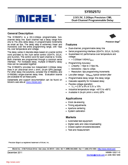
SY89297U2.5/3.3V, 3.2Gbps Precision CML Dual-Channel Programmable DelayPrecision Edge is a registered trademark of Micrel, Inc.Micrel Inc. • 2180 Fortune Drive • San Jose, CA 95131 • USA • tel +1 (408) 944-0800 • fax + 1 (408) 474-1000 •General DescriptionThe SY89297U is a DC-3.2Gbps programmable, two-channel delay line. Each channel has a delay range from 2ns to 7ns (5ns delta delay) in programmable increments as small as 5ps. The delay step is extremely linear and monotonic over the entire programming range, with 15ps INL over temperature and voltage.The delay varies in discrete steps based on a serial control word provided by the 3-pin serial control (SDATA, SCLK, and SLOAD). The control word for each channel is 10-bits. Both channels are programmed through a common serial interface. For increased delay, multiple SY89297U delay lines can be cascaded together.The SY89297U provides two independent 3.2Gbps delay lines in an ultra-small 4mm x 4mm, 24-pin QFN package. For other delay line solutions, consider the SY89295U and SY89296U single-channel delay lines. Evaluation boards are available for all these parts.Datasheets and support documentation can be found on Micrel’s web site at: .Precision Edge ®Features• Dual-channel, programmable delay line• Serial programming interface (SDATA, SCLK, SLOAD) • Guaranteed AC performance over temperature and voltage:– > 3.2Gbps/1.6GHz f MAX • Programming Accuracy: – Linearity: −15ps to +15ps INL – Monotonic: −5ps to +25ps– Resolution: 5ps programming increments • Low-jitter design: 1ps RMS typical random jitter • Programmable delay range: 5ns delay range • Cascade capability for increased delay • Flexible voltage operation:– V CC = 2.5V ± 5% or 3.3V ± 10% • Industrial temperature range: −40°C to +85°C • Available in 24-pin (4mm x 4mm) QFNApplications• Clock de-skewing • Timing adjustments • Aperture centering • System calibrationMarkets• Automated test equipment• Digital radio and video broadcasting • Closed caption encoders/decoders • Test and measurementOrdering Information(1)Part Number Package Type Operating Range Package Marking Lead FinishSY89297UMG QFN-24 Industrial 297U with Pb-Free Bar Line Indicator Pb-Free NiPdAuSY89297UMGTR(2)QFN-24 Industrial 297U with Pb-Free Bar-Line Indicator Pb-Free NiPdAuNotes:1. Contact factory for die availability. Dice are guaranteed at T= 25°C, DC electricals only.A2. Tape and Reel.Pin Configuration24-Pin QFNTruth TablesInputs Outputs INA, INB /INA, /INB QA, QB /QA, /QB0 1 0 11 0 1 0Table 1. Inputs/Outputs/ENA, /ENB Q, /Q (A, B)1 Q = Low, /Q = HIGH0 IN, /IN Delayed (normal operation)Table 2. Input Enable (Latches Outputs)Functional Block DiagramPin DescriptionPin NumberPin Name Pin Function1 2INA /INAChannel A Differential Input: INA and /INA pins receive the Channel A data. QA and /QA are the delayed product of INA and /INA. Each input is internally terminated to VTA through a 50Ω resistor (100Ω across INA and /INA).3 VTA Input A Termination Center-Tap: Each side of the differential input pair terminates to this pin.This pin provides a center-tap to a termination network for maximum interface flexibility. See“Input Interface Applications” section. 4 VTBInput B Termination Center-Tap: Each side of the differential input pair terminates to this pin. This pin provides a center-tap to a termination network for maximum interface flexibility. See “Input Interface Applications” section. 5 6INB /INBChannel B Differential Input: INB and /INB pins receive the Channel B data. QB and /QB are the delayed product of INB and /INB. Each input is internally terminated to VTB through a 50Ω resistor (100Ω across INB and /INB).7 VREF-ACReference Voltage Output: For AC-coupled input signals, this pin can bias the inputs IN and /IN. Connect VREF-AC directly to the VT input pin for each channel. De-couple to V CC using a0.01µF capacitor. Maximum sink/source current is ±0.5mA. For DC-coupled input applications, leave VREF-AC pin floating. 8, 11, 20GND, Exposed PadNegative Supply: Exposed pad must be connected to a ground plane that is the same potential as the ground pins.9 /ENACMOS/TTL-Compatible Enable Input: When the /ENA pin is pulled HIGH, QA is held LOW and /QA goes HIGH after the programmed delay propagates through the part. /ENA contains a 67k Ω pull-down resistor and defaults LOW when left floating. Logic threshold level is V CC /2 10 /ENBCMOS/TTL-Compatible Enable Input: When the /ENB pin is pulled HIGH, QB is held LOW and /QB goes HIGH after the programmed delay propagates through the part. /ENB contains a 67k Ω pull-down resistor and defaults LOW when left floating. Logic threshold level is Vcc/2 12, 15, 16, 19VCC Power Supply: Bypass each supply pin with 0.1µF//0.01µF low-ESR capacitors. See DC Electrical Characteristics table for more details. 2.5V ±5% or 3.3V ±10%.13 14 /QB QB CML Differential Output: QB and /QB are the delayed product of INB, /INB. CML outputs are terminated at the destination with 100Ω across the pair. See “CML Output Termination” section.17 18/QA QACML Differential Output: QA and /QA are the delayed product of INA, /INA. CML outputs are terminated at the destination with 100Ω across the pair. See “CML Output Termination” section.23 22SCLK SDATACMOS/TTL-compatible 3-pin serial programming control inputs: The 3-pin serial control sets each channel’s IN to Q delay. DA(0:9) control channel A delay. DB(0:9) control channel B. To program the two channels, insert a 20-bit word (DA0:DA9 and DB0:DB9) into SDATA and clock in the control bits with SCLK. Maximum input frequency to SCLK is 40MHz. Data is loaded into the serial registers on the L-H transition of SCLK. After all 20-bits are clocked in, SLOAD latches the new delay bits. These pins have internal pull-downs at the inputs. See “ACElectrical Characteristics” for delay values. Logic threshold level is Vcc/2. SCLK and SDATA contain a 67k Ω pull-down resistor and default LOW when left floating.24 SLOADCMOS/TTL-compatible 3-pin serial programming control input: SLOAD controls the latches that transfer scanned data to the delay line. These latches are transparent when SLOAD is high. Data transfers from the latch to the delay line on a L-H transition of SLOAD. SLOAD has to transition H-L before new data is loaded in the scan chain. When SLOAD is high, the latches are transparent and SCLK cannot switch. Otherwise, new data will immediately transfer to the scan chain. Logic threshold level is Vcc/2. SLOAD contains a 67k Ω pull-down resistor and defaults LOW when left floating. 21 SOUTCMOS/TTL-compatible output: This pin is used to support cascading multiple SY89297U delay lines. Serial data is clocked into the SDATA input and is clocked out of SOUT into the next SY89297U delay line. SOUT pin includes an internal 550Ω pull-up resistor.Absolute Maximum Ratings(1)Supply Voltage (V CC) .................................. –0.5V to +4.0V Input Voltage (V IN) .......................................... –0.5V to V CC CML Output Voltage (V OUT)… ....... V CC −1.0V to V CC +0.5V Current (V T)Source or Sink Current on VT pin ..................... ±70mA Input CurrentSource or Sink Current on (IN, /IN) .................. ±35mA Current (V REF)Source or sink current on V REF-AC(2) ................ .±0.5mA Maximum operating Junction Temperature ............ 125°C Lead Temperature (soldering, 20sec.) ..................... 260°C Storage Temperature (T s) ....................... –65°C to +150°C Operating Ratings(3)Supply Voltage (V CC)T A (−40°C to +85°C) ................ +2.375V to +2.625VT A (−40°C to +75°C) .......................... +3.0V to 3.6V Ambient Temperature (T A) .......................... −40°C to +85°C Package Thermal Resistance(4)QFN (θJA)Still-Air...............................................................43°C/W QFN (ψJB)Junction-to-Board...........................................30.5°C/WDC Electrical Characteristics(5)T A = −40°C to +85°C, Channels A and B, unless otherwise stated.Symbol Parameter Condition Min. Typ. Max. UnitsV CC Power Supply Voltage Range T A: −40°C to +85°C 2.375 2.5 2.625 V T A: −40°C to +75°C 3.0 3.3 3.6 V T A: −40°C to +85°C,Airflow = 500 LFPM3.0 3.3 3.6 VI CC PowerSupplyCurrent Maximum V CC, Both ChannelsCombined, Output Load Included195 250 mAR IN Input Resistance(IN-to-VT, /IN-to-VT)455055ΩR DIFF_IN Differential Input Resistance(IN-to-/IN)90100110ΩV IH Input HIGH Voltage (IN, /IN) 1.2 V CC V V IL Input LOW Voltage (IN, /IN) 0 V IH–0.1 V V IN Input Voltage Swing (IN, /IN) See Figure 5a 0.1 1.0 VV DIFF_IN Differential Input Voltage Swing(|IN - /IN|)See Figure 5b 0.2 VV REF-AC Output Reference Voltage V CC–1.3 V CC–1.2 V CC–1.1 VV T_IN Voltage from Input to V T 1.28 V Notes:1. Permanent device damage may occur if “Absolute Maximum Ratings” are exceeded. This is a stress rating only and functional operation is notimplied at conditions other than those detailed in the operational sections of this data sheet. Exposure to “Absolute Maximum Rating” conditions for extendedperiodsmayaffectdevicereliability.2. Due to the limited drive capability, use for input of the same package only.3. The data sheet limits are not guaranteed if the device is operated beyond the operating ratings.4. Thermal performance on QFN packages assumes exposed pad is soldered (or equivalent) to the device most negative potential (GND).5. The circuit is designed to meet the DC specifications shown in the table after thermal equilibrium has been established.CML Outputs DC Electrical Characteristics (6)V CC = +2.5V +5% or +3.3V ±10%, R L = 100Ω across the outputs; T A = −40°C to +85°C, unless otherwise stated. Symbol Parameter Condition Min. Typ. Max. Units V OH Output HIGH Voltage R L = 50Ω to V CC V CC −0.020 V CC −0.010V CC VV OUT Output Voltage SwingSee Figure 5a 325 400 mV V DIFF_OUTDifferential Output Voltage SwingSee Figure 5b650 800 mV R OUT Output Source Impedance455055ΩLVTTL/CMOS DC Electrical Characteristics (6)V CC = +2.5V +5% or 3.3V ±10%, T A = −40°C to +85°C, unless otherwise stated. Symbol Parameter Condition Min. Typ. Max. Units V IH Input HIGH Voltage 2.0 V V IL Input LOW Voltage0.8 V I IH Input HIGH Current V IH = VCC 150 µA I IL Input LOW Current V IL = 0.8V50µAV OLOutput LOW Voltage SOUT Pin; I OL =1mA 0.55 VOutput High Leakage CurrentSOUT = V CC 100 µANote:6. The circuit is designed to meet the DC specifications shown in the above table after thermal equilibrium has been established.AC Electrical Characteristics (7)T A = −40°C to +85°C, Channels A and B, unless otherwise stated. Symbol Parameter ConditionMin. Typ. Max. Units f MAXMaximum Operating FrequencyClock: V out Swing >200mV pk 1.6 GHzNRZ Data3.2Gbpst pdPropagation Delay IN to Q; D[0–9]=0 IN to Q; D[0–9]=1023/EN to Q: D[0–9]=0; V TH = V CC /2 SDATA to SOUT (D0–D9=Low), No load1000 5500 1000 20002000 7500 2500 4500pst RANGE Programmable Ranget pd (max) – t pd (min)4150 5115 pst SKEWDuty Cycle Skew t PHL – t PLH Note 84555%AC Electrical Characteristics(7)T A = −40°C to +85°C, Channels A and B, unless otherwise stated.Symbol Parameter Condition Min. Typ. Max. UnitsΔt Step DelayD0 HighD1 HighD2 HighD3 HighD4 HighD5 HighD6 HighD7 HighD8 HighD9 HighD0-D9 High510204080160320640128025605115ps Monotonic −5 25INL IntegralNon-Linearity Note 9 −15 +15 pst S Setup TimeSDATA to SCLKSCLK to SLOAD/EN to INNote 10Note 11400400300pst H Hold TimeSLOAD to SCLKIN to /ENSCLK to SDATANote 12Note 13300−100200pst PW Pulse Width SLOAD 1000 ps t R Release Time /EN to IN Note 14 800 pst JITTER Cycle-to-Cycle JitterTotal JitterRandom JitterNote 15Note 16Note 172202ps RMSps PPps RMSt r, t f Output Rise/Fall Time 20% to 80% (Q) 30 55 80 ps Duty Cycle Input Frequency = 1.6GHz 45 55 % Notes:7. High frequency AC electricals are guaranteed by design and characterization.8. Duty cycle skew guaranteed only for differential operation measured from the cross point of the input to the crosspoint of the output.9. INL (Integral Non-Linearity) is defined from its corresponding point on the ideal delay versus D[9:0] curve as the deviation from its ideal delay. Themaximum difference is the INL. Theoretical Ideal Linearity (TIL) = (measured maximum delay – measured minimum delay) ÷ 1023. INL = measured delay – (measured minimum delay + (step number x TIL)).10. SCLK has to transition L-H a setup time before the SLOAD H-L transition to ensure the valid data is properly latched. See timing diagram "Setupand Hold Time: SCLK and SLOAD.”11. This setup time is the minimum time that /EN must be asserted prior to the next transition of IN / /IN to prevent an output response greater than±75 mV to that IN or /IN transition. See timing diagram Setup, Hold and Release Time: IN and /EN."12. SCLK has to transition L-H a hold time after the SLOAD H-L transition to ensure that the valid data is properly latched before starting to load newdata. See timing diagram "Setup and Hold Time: SCLK and SLOAD.”13. This hold time is the minimum time that /EN must remain asserted after a negative going transition of IN to prevent an output response greater than+75mv to the IN transition. See timing diagram “Setup, Hold, and Release Time: IN and /EN.”14. This release time is the minimum time that /EN must be de-asserted prior to the next IN / /IN transition to affect the propagation delay of IN to Qless than 1ps. See timing diagram “Setup, Hold, and Release Time: IN and /EN.”15. Cycle-to-cycle jitter definition: The variation of periods between adjacent cycles over a random sample of adjacent cycle pairs.T jitter_cc = T n – T n+1, where T is the time between rising edges of the output signal.16. Total jitter definition: With an ideal clock input, no more than one output edge in 1012 output edges will deviate by more than the specified peak-to-peak jitter value.17. Random jitter definition: Jitter that is characterized by a Gaussian distribution, unbounded and is quantified by its standard deviation and mean.Random jitter is measured with a K28.7 comma defect pattern, measured at 1.5Gbps.Timing DiagramsFigure 1. Setup and Hold Time: SDATA and SCLKFigure 2. Setup and Hold Time: SCLK and SLOADTiming Diagrams (Continued)Figure 3. Set-Up, Hold, and Release Time: IN and /ENFigure 4. SLOAD Pulse Width (TPW)Typical Operating CharacteristicsV CC = +2.5V, GND = 0V, V IN = 100mV, R L = 100Ω across the outputs, T A = 25°C.Phase Noise ChartV CC = +2.5V, GND = 0V, V IN = 100mV, R L = 100Ω across the outputs, T A = 25°C.f C: 1GHz Delay Setting: 00001 00110 (2ns)分销商库存信息:MICRELSY89297UMH SY89297UMG SY89297UMG TR SY89297UMH TR。
维沙耶芯片电阻说明书

Document Number: 28744For technical questions, contact: *************************** MCS 0402 VG01, MCT 0603 VG01, MCU 0805 VG01 andMCA 1206 VG01 thin film flat chip resistors with establishedreliability are the perfect choice for all high-reliabilityapplications typically found in military, aircraft and spacecraftelectronics. These versions supplement the families ofprofessional and precision thin film flat chip resistorsMCS 0402, MCT 0603, MCU 0805 and MCA 1206.∙Established reliability, failure rate level E6∙Advanced thin film technology ∙Pure Sn termination on Ni barrier layer ∙Single lot date code ∙Material categorization: For definitions of complianceplease see /doc?99912APPLICATIONS∙Military ∙Avionics ∙Space Notes•These resistors do not feature a limited lifetime when operated within the permissible limits. However, resistance value drift increasing over operating time may result in exceeding a limit acceptable to the specific application, thereby establishing a functional lifetime.•The failure rate level E6 (10-6/h, πQ = 0.3), corresponding to MIL Level P, is superior to level E5 (10-5/h, πQ = 1) and thus may be used as areplacement.METRIC SIZE IMPERIAL0402060308051206EN/CECC RR1005M RR1608M RR2012M RR3216M TECHNICAL SPECIFICATIONSDESCRIPTIONMCS 0402 VG01MCT 0603 VG01MCU 0805 VG01MCA 1206 VG01EN/CECC style (size)RR1005M RR1608M RR2012M RR3216MResistance range10 Ωto 1 M Ω; 0Ω 1 Ωto 1 M Ω; 0ΩResistance tolerance± 1 %; ± 0.1 %T emperature coefficient± 50ppm/K; ± 15 ppm/K Rated dissipation, P 700.063W 0.1W 0.125W 0.25W Operating voltage, U max. AC/DC50V 75 V 150V 200V Permissible film temperature, ϑF max.125︒C Operating temperature range- 55 °C to 125 °C Max. resistance change at P 70for resistance range, |∆R /R| max. after:10 Ωto 1 M Ω 1 Ωto 1 M Ω1000h≤ 0.25 %8000h≤ 0.5 %225000h≤ 1.5 %Permissible voltage against ambient(insulation):1 min; U ins75V 100V 200V 300V Continuous75V 75V 75V 75V Assessed failure rate levelE6 = 10-6/h Quality factor, πQ0.3Failure rate: FIT observed < 0.1 x 10⁻⁹/h For technical questions, contact: ***************************Document Number: 28744Notes•The products can be ordered using either the PART NUMBER or the PRODUCT DESCRIPTION.•Products within a packaging unit are single lot date code.TYPE/SIZEVERSION TCR RESISTANCE TOLERANCE PACKAGING MCS 0402MCT 0603MCU 0805MCA 1206H = EN 140401-801,“Version E”;failure rate level E6 C = ± 50 ppm/K E = ± 15 ppm/K Z = Jumper 3 digit value 1 digit multiplier MULTIPLIER8 = *10-29 = *10-10 = *1001 = *1012 = *1023 = *1034 = *1040000 = Jumper F = ± 1 %B = ± 0.1 %Z = JumperE1E0P1P5Product Description: MCT 0603-50 1% VG01 P5 287KProduct Description: MCT 0603 VG01 P5 0R0MCT 0603-50 1 %VG01P5287K MCT 0603--VG01P50R0TYPE/SIZETCR T OLERANCE VERSION PACKAGING RESISTANCE MCS 0402MCT 0603MCU 0805MCA 1206± 50 ppm/K ± 15 ppm/K ± 1 %± 0.1 %VG01 = EN 140401-801,“Version E”;failure rate level E6E1E0P1P549R9 = 49.9 Ω287K = 287 k Ω0R0 = JumperMC T 0603H Z 0000Z P 50006032873500Document Number: 28744For technical questions, contact: *************************** Note•The ordering information according to EN 140401-801:2007 shown above succeeds and replaces the ordering information according to earlier versions of the detail specification EN 140401-801 or its predecessor CECC 40401-801, for example:CECC 40401-801 EZ RR1608M C 287K F E6CECC 40401-801 S RR1608M C 287K F E6with EZ; S Assessment level, where EZ is successor to and superior replacement for SRR1608M Style, with suffix M for “metric”C Temperature coefficient, according to the detail specificationC = ± 50 ppm/K; E = ± 15 ppm/K Note•According to EN 140401-801, resistance values are to be selected from the E96 series for ±1% tolerance and from the E192 series for ±0.1 % tolerance.EN140401-801EZRR1608M-0R00-E6The elements used in the component number have the following meaning:EN140401-801EZRR1608MR287KF E6EN detail specification number Assessment level for the zero-defect approach Style (size)T emperature coefficient, according to EN 60062R = ± 50 ppm/K; P = ± 15 ppm/K Resistance, according to EN 60062, 4 characters T olerance on rated resistance, according to EN 60062F = ± 1 %; B = ± 0.1 %Failure rate level according to EN 60115-1, annex ZRTEMPERATURE COEFFICIENT AND RESISTANCE RANGEDESCRIPTIONRESISTANCE TCRTOLERANCE MCS 0402 VG01MCT 0603 VG01MCU 0805 VG01MCA 1206 VG01± 50 ppm/K± 1 %10 Ωto 1 M Ω 1 Ωto 1 M Ω1Ωto 1 M Ω1Ωto 1 M Ω± 15 ppm/K± 0.1 %100Ωto 33.2 k Ω100Ωto 47.5 k Ω100Ωto 100k Ω43.2Ωto 332k ΩJumper ≤ 20m Ω; I max. = 0.63 A ≤ 20m Ω; I max. = 1 A ≤ 20m Ω; I max. = 1.5 A≤ 20m Ω; I max. = 2 A PACKAGINGTYPECODE QUANTITY CARRIER TAPE WIDTH PITCH REEL DIAMETER MCS 0402 VG01E11000Paper tape acc. IEC 60286-3T ype I 8 mm 2 mm 180 mm/7"E010 000MCT 0603 VG01P110008 mm 4 mm P55000MCU 0805 VG01P11000P55000MCA 1206 VG01P11000P55000 For technical questions, contact: ***************************Document Number: 28744Note•Resistors MCA 1206 VG01 and MCU 0805 VG01 are marked using to the four-character code system of IEC 60062, 4.2.3.Resistors MCT 0603 VG01 and MCS 0402 VG01 do not show any marking on their light blue protective coating.Note•The given solder pad dimensions reflect the considerations for board design and assembly as outlined e.g. in standards IEC 61188-5-x, or in publication IPC 7351. They do not guarantee any supposed thermal properties, however, they will be found adequate for most general applications.DIMENSIONS AND MASSTYPEH (mm)L (mm)W (mm)W T (mm)T b (mm)T t (mm)MASS (mg)MCS 0402 VG010.32 ± 0.05 1.0 ± 0.050.5 ± 0.05> 75 % of W 0.2 ± 0.10.2 + 0.1/- 0.150.6MCT 0603 VG010.45 + 0.1/- 0.05 1.55 ± 0.050.85 ± 0.10.3 + 0.15/- 0.21.9MCU 0805 VG010.45 + 0.1/- 0.052.0 ± 0.11.25 ± 0.150.4 + 0.1/- 0.2 4.6MCA 1206 VG010.55 ± 0.1 3.2 + 0.1/- 0.2 1.6 ± 0.150.5 ± 0.259.2RECOMMENDED SOLDER PAD DIMENSIONSTYPE WAVE SOLDERINGREFLOW SOLDERING G(mm)Y (mm)X (mm)Z (mm)G (mm)Y (mm)X (mm)Z(mm)MCS 0402 VG01----0.350.550.55 1.45MCT 0603 VG010.551.10 1.102.750.650.700.95 2.05MCU 0805 VG010.801.25 1.50 3.300.900.90 1.402.70MCA 1206 VG011.40 1.50 1.90 4.40 1.50 1.15 1.753.80grade ceramic (Al2O3) substrate and conditioned to achieve the desired temperature coefficient. Specially designed inner contacts are deposited on both sides. A special laser is used to achieve the target value by smoothly cutting a meander groove in the resistive layer without damaging the ceramics. For the high ohmic range, optimized cermet products provide comparable properties. The resistor elements are covered by a protective coating designed for electrical, mechanical and climatic protection. The terminations receive a final pure tin on nickel plating.The result of the determined production is verified by an extensive testing procedure performed on 100 % of the individual resistors. This includes pulse load screening for the elimination of products with a potential risk of early life failures according to EN 140401-801, 2.1.2.2 (feasible for R≥ 10 Ω). Only accepted products are laid directly into the paper tape in accordance with EN 60286-3 (3), Type I.Products within a packaging unit are from the same production lot and carry the same date code.ASSEMBLYThe resistors are suitable for processing on automatic SMD assembly systems. They are suitable for automatic soldering using wave, reflow or vapour phase as shown in IEC61760-1 (3). Solderability is specified for 2 years after production or requalification. The permitted storage time is 20 years.The resistors are RoHS compliant; the pure tin plating provides compatibility with lead (Pb)-free soldering processes. The immunity of the plating against tin whisker growth has been proven under extensive testing.The encapsulation is resistant to all cleaning solvents commonly used in the electronics industry, including alcohols, esters and aqueous solutions. The suitability of conformal coatings, if applied, shall be qualified by appropriate means to ensure the long-term stability of the whole system.∙2000/53/EC End of Vehicle life Directive (ELV) and Annex II (ELV II)∙2011/65/EU Restriction of the use of Hazardous Substances directive (RoHS)∙2002/96/EC Waste Electrical and Electronic Equipment Directive (WEEE)APPROVALSThe resistors are approved within the IECQ-CECC Quality Assessment System for Electronic Components to the detail specification EN140401-801 which refers to EN60115-1, EN140400 and the variety of environmental test procedures of the IEC 60068 (3)series.Conformity is attested by the use of the CECC logo () as the mark of conformity on the package label.Vishay BEYS C HLAG has achieved “Approval of Manufacturer” in accordance with IEC QC001002-3, clause 2. The release certificate for “Technology Approval Schedule” in accordance with CECC240001 based on IEC QC001002-3, clause 6 is granted for the Vishay BEYSCHLAG manufacturing process.The Vishay BEYSC HLAG production facility is registered with the CAGE code D9539.RELATED PRODUCTSA wider range of TCR, tolerance and resistance values, plus the option of values from a different E series is available with products approved to EN 140401-801, Version A, without established reliability, nominal failure rate level E0 (quality factor πQ = 3). See the datasheets:∙“Professional Flat Chip Resistors”(/doc?28705)∙“Precision Flat Chip Resistors”(/doc?28700)Notes(1)Global Automotive Declarable Substance List, see .(2)CEFIC (European Chemical Industry Council), EECA (European Electronic Component Manufacturers Association), EICTA (European tradeorganisation representing the information and communications technology and consumer electronics), see /index.php?id=1053&id_article=340.(3)The quoted IEC standards are also released as EN standards with the same number and identical contents.Document Number: 28744For technical questions, contact: *************************** For technical questions, contact: ***************************Document Number: 28744Document Number: 28744For technical questions, contact: *************************** •“Precision Flat Chip Resistors”, document no. 28700EN 140400, sectional specificationEN 140401-801, detail specificationFor further information on the tests and requirements ofthese products please refer to the specifications mentionedabove, and to the following datasheets:•“Professional Flat Chip Resistors”(/doc?28705)•“Precision Flat Chip Resistors”(/doc?28700)HISTORICAL 12NC INFORMATION∙The resistors had a 12-digit code starting with 2312∙The subsequent 4 digits indicated the resistor type,specification and packaging; see the 12NC table∙The remaining 4digits indicate the resistance value:-The first 3digits indicated the resistance value-The last digit indicated the resistance decade inaccordance with the resistance decade table RESISTANCE DECADE Historical 12NC ExampleThe 12NC of a MC T 0603 VG01 resistor, value 287K andTCR 50 with ± 1 % tolerance, supplied in cardboard tape of5000units per reel was: 2312 215 02874.RESISTANCE DECADE LAST DIGIT 1Ω to 9.99Ω810Ω to 99.9Ω9100Ω to 999Ω11 k Ωto 9.99k Ω210k Ω to 99.9k Ω3100k Ω to 999k Ω41M Ω5HISTORICAL 12NC - Resistor type and packagingDESCRIPTION2312........CARDBOARD TAPE ON REEL TYPE TCRTOL.E1 1000 PIECES E0 10 000 PIECES MCS 0402 VG01± 50 ppm/K± 1 %260 0....275 0....± 15 ppm/K± 0.1 %262 0....277 0....Jumper262 90001277 90001TYPE TCRTOL.P11000 PIECES P5 5000 PIECES PW 20 000 PIECES MCT 0603 VG01± 50 ppm/K± 1 %200 0....215 0....205 0....± 15 ppm/K± 0.1 %202 0....217 0....-Jumper202 90001217 90001207 90001MCU 0805 VG01± 50 ppm/K±1 %240 0....255 0....245 0....± 15 ppm/K± 0.1 %242 0....257 0....-Jumper242 90001257 90001247 90001MCA 1206 VG01± 50 ppm/K± 1 %No 12NC assigned to MCA 1206 VG01± 15 ppm/K± 0.1 %Jumper“Vishay”), disclaim any and all liability for any errors, inaccuracies or incompleteness contained in any datasheet or in any other disclosure relating to any product.Vishay makes no warranty, representation or guarantee regarding the suitability of the products for any particular purpose or the continuing production of any product. To the maximum extent permitted by applicable law, Vishay disclaims (i) any and all liability arising out of the application or use of any product, (ii) any and all liability, including without limitation special, consequential or incidental damages, and (iii) any and all implied warranties, including warranties of fitness for particular purpose, non-infringement and merchantability.Statements regarding the suitability of products for certain types of applications are based on Vishay’s knowledge of typical requirements that are often placed on Vishay products in generic applications. Such statements are not binding statements about the suitability of products for a particular application. It is the customer’s responsibility to validate that a particular product with the properties described in the product specification is suitable for use in a particular application. Parameters provided in datasheets and/or specifications may vary in different applications and performance may vary over time. All operating parameters, including typical parameters, must be validated for each customer application by the customer’s technical experts. Product specifications do not expand or otherwise modify Vishay’s terms and conditions of purchase, including but not limited to the warranty expressed therein.Except as expressly indicated in writing, Vishay products are not designed for use in medical, life-saving, or life-sustaining applications or for any other application in which the failure of the Vishay product could result in personal injury or death. Customers using or selling Vishay products not expressly indicated for use in such applications do so at their own risk. Please contact authorized Vishay personnel to obtain written terms and conditions regarding products designed for such applications. No license, express or implied, by estoppel or otherwise, to any intellectual property rights is granted by this document or by any conduct of Vishay. Product names and markings noted herein may be trademarks of their respective owners.Material Category PolicyVishay Intertechnology, Inc. hereby certifies that all its products that are identified as RoHS-Compliant fulfill the definitions and restrictions defined under Directive 2011/65/EU of The European Parliament and of the Council of June 8, 2011 on the restriction of the use of certain hazardous substances in electrical and electronic equipment (EEE) - recast, unless otherwise specified as non-compliant.Please note that some Vishay documentation may still make reference to RoHS Directive 2002/95/EC. We confirm that all the products identified as being compliant to Directive 2002/95/EC conform to Directive 2011/65/EU.Vishay Intertechnology, Inc. hereby certifies that all its products that are identified as Halogen-Free follow Halogen-Free requirements as per JEDEC JS709A standards. Please note that some Vishay documentation may still make reference to the IEC 61249-2-21 definition. We confirm that all the products identified as being compliant to IEC 61249-2-21 conform to JEDEC JS709A standards.Revision: 02-Oct-121Document Number: 91000。
NI 5783 Four Channel Transceiver Adapter Module 的说
DEVICE SPECIFICATIONSNI 5783Four Channel Transceiver Adapter ModuleThis document lists specifications for the NI 5783 adapter module. Pair these specifications with the specifications listed in your FlexRIO FPGA module specifications document or your Controller for FlexRIO specifications document.Caution The protection provided by the NI 5783 can be impaired if it is used in amanner not described in this document.Caution To avoid permanent damage to the NI 5783, disconnect all signalsconnected to the NI 5783 before powering down the module, and only connectsignals after the module has been powered on by the FlexRIO FPGA module or theController for FlexRIO.Note All numeric specifications are typical unless otherwise noted. All graphsillustrate the performance of a representative module.Specifications are subject to change without notice. For the most recent device specifications, visit /manuals.ContentsFlexRIO Documentation (2)Analog Input (3)General Characteristics (3)Typical Specifications (4)Analog Output (9)General Characteristics (9)Typical Specifications (10)CLK/REF IN (13)TRIG General Characteristics (14)AUX I/O (Port 0 DIO <0..3>, Port 1 DIO <0..3>, and PFI <0..3> (15)Power (15)Physical (15)Environment (16)Operating Environment (16)Storage Environment (16)Shock and Vibration (16)Compliance and Certifications (17)Safety (17)Electromagnetic Compatibility (17)CE Compliance (17)Online Product Certification (18)Environmental Management (18)FlexRIO Documentation2| | NI 5783 SpecificationsTable 1. FlexRIO Documentation Locations and Descriptions (Continued)Analog InputGeneral CharacteristicsNumber of channels Four, single-ended, simultaneously sampled Connector Type HDBNC (high-density BNC)Input type50 ΩInput coupling DCNI 5783 Specifications| © National Instruments| 3Sample rateInternal Sample Clock100 MHzExternal Sample Clock60 MHz to 100 MHzAnalog-to-digital converter (ADC)Type Quad, 16-bitPart number AD9653Related InformationFor more information about the ADC, refer to the AD9653 datasheet at . Typical SpecificationsFull-scale input range (normal operating conditions)Elliptic 2.030 V pk-pkButterworth 2.037 V pk-pkDC accuracyElliptic±[(0.80% × reading) + 3.5 mV]Butterworth±[(1.00% × reading) + 3.75 mV]Input impedanceElliptic50 Ω ± 0.5%Butterworth50 Ω ± 0.8%Bandwidth (-3 dB)Elliptic39.4 MHzButterworth39.5 MHzNote All AI spectral performance values apply to both the Elliptic and Butterworthvariants.1Measured at 10.1 MHz with a -1 dBFS signal adjusted to full-scale.2Calculated from SINAD corrected to fullscale.3Measured at 10.1 MHz with a -1 dBFS signal.4| | NI 5783 SpecificationsTable 3. AI Noise Spectral DensityNote All AI channel crosstalk values apply to both the Elliptic and Butterworth variants.Figure 1. AI CrosstalkAmplitude(dBc)Frequency (Hz)NI 5783 Specifications| © National Instruments| 5Figure 2. AI Frequency Response (Zoomed Out)N o r m a l i z e d A m p l i t u d e t o 100 k H z (d B )Frequency (Hz)Figure 3. AI Frequency Response (Zoomed In)N o r m a l i z e d A m p l i t u d e t o100 k H z (d B )Frequency (Hz)6 | | NI 5783 SpecificationsFigure 4. AI Step Response (Butterworth)A m p l i t u d e (V )1–50 m050 m100 m 150 m 200 m 250 m 300 m 350 m 400 m 450 m 500 m 550 m 600 m 650 m 700 m 750 m 800 m 850 m 900 m 950 m Time (ns)20020–10406080100120140160180Figure 5. AI Step Response (Elliptic)A m p l i t u d e (V )–50 m050 m100 m 150 m 200 m 250 m 300 m 350 m 400 m 450 m 500 m 550 m 600 m 650 m 700 m 750 m 800 m 850 m 900 m 950 m 1Time (ns)20020–10406080100120140160180NI 5783 Specifications | © National Instruments | 7Figure 6. AI Spectral (10.1 MHz at -1 dBFS input signal, 6.1 kHz RBW, 10 Averages)A m p l i t u d e (dB F S )0–120–115–110–105–100–95–90–85–80–75–70–65–60–55–50–45–40–35–30–25–20–15–10–5Frequency (Hz)50 M0 2 M6 M10 M14 M18 M22 M26 M30 M34 M38 M42 M46 MNote AI Spectral figure applies to both the Elliptic and Butterworth variants.Figure 7.AI Return LossA m p l i t u d e (dB )Frequency (Hz)8 | | NI 5783 SpecificationsAnalog OutputGeneral CharacteristicsNumber of channels Four, single-ended, simultaneously updated Connector type HDBNC (high-density BNC)Output type50 ΩOutput coupling DCDigital-to-analog converter (DAC)Type Quad, 16-bitPart number DAC3484Minimum analog input to analog output response time4100 MS/s1130 ns200 MS/s720 ns400 MS/s550 nsRelated InformationFor more information about the DAC, refer to the DAC3484 datasheet at .4Minimum time to digitize a signal (AI) and output a response (AO). Time measured from signal entering the AI connector, passing into and out of the LabVIEW FPGA diagram, and observed at the AO connector.5400 MS/s with 2x interpolation is available only when operating in 2 channel analog output mode.NI 5783 Specifications| © National Instruments| 9Typical SpecificationsFull-scale output range (normal operation conditions)50 Ω 1.001 V pk-pk High-Z2.002 V pk-pkDC accuracy (into High-Z)±[(2.0% × desired voltage) + 4.4 mV]Output impedance 50 Ω ± 0.7%SFDR 6-81 dBcTable 6. AO Noise Spectral Density (into 50 Ω)Table 7. AO Channel Crosstalk (10 MHz)Figure 8. AO Crosstalk (into 50 Ω Load)A m p l i t u d e (dB c )Frequency (Hz)610.1 MHz tone at -1 dBFS.10 | | NI 5783 SpecificationsFigure 9. AO Frequency Response Across Data RateN o r m a l i z e d A m p l i t u d e t o 100 k H z (d B )0–10–9.5–9.0–8.5–8.0–7.5–7.0–6.5–6.0–5.5–5.0–4.5–4.0–3.5–3.0–2.5–2.0–1.5–1.0–0.5Frequency (Hz)Figure 10. AO Phase Noise (Signal at 12.1 MHz)A m p l i t u d e (dB c /H z )–95–155–150–145–140–135–130–125–120–115–110–105–100Offset from Carrier (Hz)1 M101001 k10 k100 k–160NI 5783 Specifications | © National Instruments | 11Figure 11. AO Return LossA m p l i t u d e (dB )0–32–30–28–26–24–22–20–18–16–14–12–10–8–6–4–2Frequency (Hz)300 M10 M40 M60 M80 M 100 M 120 M 140 M 160 M 180 M 200 M 220 M 240 M 260 M 280 M Figure 12. AO Two Tone, Each T one at -7 dBFS, 69.95 MHz, and 70.05 MHz, 500 HzRBW0–95–90–85–80–75–70–65–60–55–50–45–40–35–30–25–20–15–10–5Frequency (Hz)70.5 M69.5 M69.6 M 69.7 M 69.8 M 69.9 M 70.0 M 70.1 M 70.2 M 70.3 M70.4 M A m p l i t u d e (d B m )Note The noise floor in the above figure is limited by the noise floor of themeasurement device. Refer to the AO Noise Spectral Density table for more information.12 | | NI 5783 SpecificationsCLK/REF INConnector type HDBNC (high-density BNC)Input impedance50 ΩInput coupling ACReference input voltage range0.75 V pk-pk to 5.2 V pk-pkSample Clock input voltage range0.4 V pk-pk to 5.2 V pk-pkAbsolute maximum voltage±8.0 VDC, 8.0 V pk-pk ACDuty cycle45% - 55%Internal VCXO phase noise10 Hz-80 dBc/Hz100 Hz-110 dBc/Hz1 kHz-140 dBc/Hz10 kHz-150 dBc/Hz100 kHz-155 dBc/Hz1 MHz-160 dBc/Hz10 MHz-162 dBc/Hz7Default clocking configuration.NI 5783 Specifications| © National Instruments| 13Figure 13. Internal Sample Clock Phase NoiseA m p l i t u d e (dB c /H z )–85–175–170–165–160–155–150–145–140–135–130–125–120–115–110–105–100–95–90Offset Frequency (from carrier)10 M101001 k10 k100 k1 MTRIG General CharacteristicsNumber of channels 1, single-ended Connector type HDBNC Coupling DCImpedanceInput 10 kΩOutput 50 ΩLogic level 3.3 V LVCMOS V oltageV IH_MIN 2 V V IL_MAX0.8 V V OH_MIN (unloaded) 3.1 V V OL_MAX (unloaded)0.2 VAbsolute maximum voltage±20 VDC, +21 dBm (7.1 V pk-pk )14 | | NI 5783 SpecificationsAUX I/O (Port 0 DIO <0..3>, Port 1 DIO <0..3>, and PFI <0..3>Number of channels12 bidirectional (8 DIO and 4 PFI) Connector type HDMIInterface standard 3.3 V LVCMOSInterface logicMaximum V IL0.8 VMinimum V IH 2.0 VMaximum V OL0.4 VMinimum V OH 2.7 VMaximum V OH 3.6 VZ out50 Ω ± 20%I out (DC)±2 mAPull-down resistor150 kΩRecommended operating voltage-0.3 V to 3.6 VOvervoltage protection±10 VMaximum toggle frequency100 MHz+5 V maximum current10 mA+5 V voltage tolerance 4.2 V to 5 VPowerTotal power, typical operation 4.6 WPhysicalDimensions12.9 x 2.0 x 12.1 cm (5.1 x 0.8 x 4.7 in.) Weight420 g (14.8 oz)Front panel connectors Ten HDBNC and one HDMINI 5783 Specifications| © National Instruments| 15EnvironmentMaximum altitude2,000 m (800 mbar) (at 25 °C ambienttemperature)Pollution Degree2Indoor use only.Operating EnvironmentAmbient temperature range0 °C to 55 °C (Tested in accordance withIEC 60068-2-1 and IEC 60068-2-2. MeetsMIL-PRF-28800F Class 3 low temperaturelimit and MIL-PRF-28800F Class 2 hightemperature limit.)Relative humidity range10% to 90%, noncondensing (Tested inaccordance with IEC 60068-2-56.) Storage EnvironmentAmbient temperature range-20 °C to 70 °C (Tested in accordancewith IEC 60068-2-1 and IEC 60068-2-2. MeetsMIL-PRF-28800F Class 3 limits.)Relative humidity range5% to 95%, noncondensing (Tested inaccordance with IEC 60068-2-56.)Shock and VibrationOperating shock30 g peak, half-sine, 11 ms pulse (Tested inaccordance with IEC 60068-2-27. MeetsMIL-PRF-28800F Class 2 limits.)Random vibrationOperating 5 Hz to 500 Hz, 0.3 g rmsNonoperating 5 Hz to 500 Hz, 2.4 g rms (Tested in accordancewith IEC 60068-2-64. Nonoperating testprofile exceeds the requirements ofMIL-PRF-28800F, Class 3.)16| | NI 5783 SpecificationsCompliance and CertificationsSafetyThis product is designed to meet the requirements of the following electrical equipment safety standards for measurement, control, and laboratory use:•IEC 61010-1, EN 61010-1•UL 61010-1, CSA 61010-1Note For UL and other safety certifications, refer to the product label or the OnlineProduct Certification section.Electromagnetic CompatibilityThis product meets the requirements of the following EMC standards for electrical equipment for measurement, control, and laboratory use:•EN 61326-1 (IEC 61326-1): Class A emissions; Basic immunity•EN 55011 (CISPR 11): Group 1, Class A emissions•EN 55022 (CISPR 22): Class A emissions•EN 55024 (CISPR 24): Immunity•AS/NZS CISPR 11: Group 1, Class A emissions•AS/NZS CISPR 22: Class A emissions•FCC 47 CFR Part 15B: Class A emissions•ICES-001: Class A emissionsNote In the United States (per FCC 47 CFR), Class A equipment is intended foruse in commercial, light-industrial, and heavy-industrial locations. In Europe,Canada, Australia, and New Zealand (per CISPR 11), Class A equipment is intendedfor use only in heavy-industrial locations.Note Group 1 equipment (per CISPR 11) is any industrial, scientific, or medicalequipment that does not intentionally generate radio frequency energy for thetreatment of material or inspection/analysis purposes.Note For EMC declarations, certifications, and additional information, refer to theOnline Product Certification section.CE ComplianceThis product meets the essential requirements of applicable European Directives, as follows:•2014/35/EU; Low-V oltage Directive (safety)•2014/30/EU; Electromagnetic Compatibility Directive (EMC)NI 5783 Specifications| © National Instruments| 17Online Product CertificationRefer to the product Declaration of Conformity (DoC) for additional regulatory compliance information. To obtain product certifications and the DoC for this product, visit / certification, search by model number or product line, and click the appropriate link in the Certification column.Environmental ManagementNI is committed to designing and manufacturing products in an environmentally responsible manner. NI recognizes that eliminating certain hazardous substances from our products is beneficial to the environment and to NI customers.For additional environmental information, refer to the Minimize Our Environmental Impact web page at /environment. This page contains the environmental regulations and directives with which NI complies, as well as other environmental information not included in this document.Waste Electrical and Electronic Equipment (WEEE)EU Customers At the end of the product life cycle, all NI products must bedisposed of according to local laws and regulations. For more information abouthow to recycle NI products in your region, visit /environment/weee.电子信息产品污染控制管理办法(中国RoHS)中国客户National Instruments符合中国电子信息产品中限制使用某些有害物质指令(RoHS)。
a1semi矽海半导体产品列表
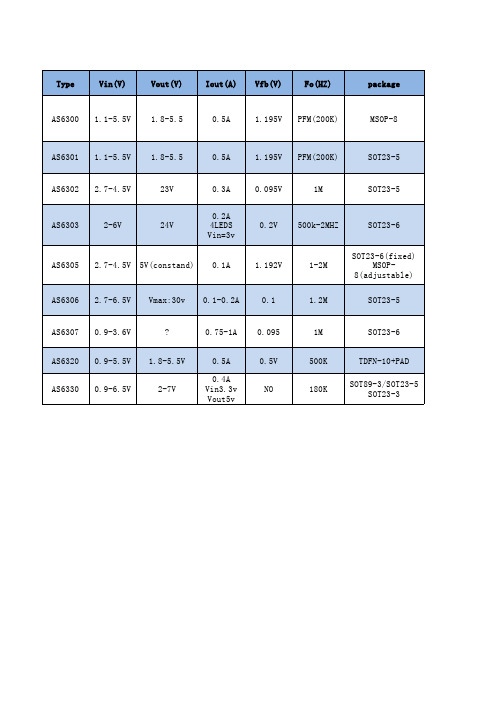
10V
1.5/1.8/2.5 /2.85V/3.3V/5.0V
5A
AS9174 1.6-6V
2A
0.8V
Fixed
1.15V
Fixed
1.16V
Fixed
1.5V
1.25V
package TO92/SOT89
replacement
TO220/TO252
TO92/SOT23-3/5
TO92/SSOOITC-283-3/5
AS1117L3 AS2815 双通道 AS2830 双通道 AS2915
AS2930
AS2930C
8V
1.5/1.8/2.5 /3.0/3.3V/ADJ
1.5-8V 2.5-5.5V
1.5/2.5/2.8V /3.3/5V/ADJ
1.2/1.5/1.8/2.5 2.85/3.3/
1.8-8V 2-6V 2-6V
AS2933 2.2-5.5V
0.8-4.5V
AS2935
2-6V
1.0-4.4V
AS2936 2.2-5.5V AS2950 2.0-5.5V AS2951 1.8-8V
1.0-4.5V
1.5/1.8/2.5 /2.8V/3.V/
1.2-4.5V
AS5102
4-7V
3.3V
0.3A 0.5A 0.3A 0.3A 0.3A 0.5A 0.5A 0.3A
ADJ
AS5428 2.5-5.5V
ADJ
AS5430 4.5V-23V
ADJ
2A
0.923V
340K
SOP8
tape&reel 2.5K
3A
0.8V
维沙BY228-13标准氧化陶瓷晶体管稳定氧化陶瓷晶体管用户手册说明书
Manuals+— User Manuals Simplified.VISHAY BY228-13 Standard Avalanche Sinterglass Diode Owner’s ManualHome » VISHAY » VISHAY BY228-13 Standard Avalanche Sinterglass Diode Owner’s ManualVISHAY BY228-13 Standard Avalanche Sinterglass DiodeFEATURESGlass passivated junctionHermetically sealed packageMaterial categorization:for definitions of compliance please see /doc?99912APPLICATIONSHigh voltage rectificationEfficiency diode in horizontal deflection circuits DESIGN SUPPORT TOOLSDESIGN SUPPORT TOOLSPARTS TABLEPART TYPE DIFFERENTIATION PACKAGE BY228-13V = 1000 V; I = 3 A SOD-64 BY228-15V = 1200 V; I = 3 A SOD-64 ABSOLUTE MAXIMUM RATINGS (T = 25 °C, unless otherwise specified)PARAMETER TEST CONDITION PART SYMBOLVALUE UNITReverse voltage See electrical characteristics BY228-13V1000VBY228-15V1200VPeak reverse voltage, non rep etitive l = 100 µABY228-13VRSM1300VBY228-15VRSM1500VPeak forward surge current t = 10 ms, half sine wave IFSM50A Average forward current IF(AV)3A Junction temperature T140°CStorage temperature range Tstg -55 to +1 75°CNon repetitive reverse avalanc he energy l = 0.4 A E10mJR F(AV)R F(AV)ambRR Rpj (BR)R RMAXIMUM THERMAL RESISTANCE (T = 25 °C, unless otherwise specified)PARAMETER TEST CONDITION SYMBOL VALUE UNITJunction ambientOn PC board with spacing 25 mmRthJA70K/WELECTRICAL CHARACTERISTICS (T = 25 °C, unless otherwise specified)PARAMETER TEST CONDITION PART SYMBO LMIN.TYP.MAX.UNITForward voltageI = 5 AV –– 1.5VReverse currentV = 1000 V BY228-13I –25µAV = 1200 VBY228-15I –25µAV = 1000 V, T = 140 °CBY228-13I ––140µAV = 1200 V, T = 140 °CBY228-15I ––140µAReverse recovery tim e I = 0.5 A, I = 1 A, i = 0.25 Atrr ––2µsTotal reverse recovery time l = 1 A, – dI /dt = 0.05 A /µstrr ––20µsTYPICAL CHARACTERISTICS (Tamb = 25 C, unless otherwise specified)Fig. 1 – Typ. Thermal Resistance vs. Lead Lengthamb amb F FR RR RR j RR j RF R R F FFig. 2 – Forward Current vs. Forward VoltageFig. 3 – Max. Average Forward Current vs. Ambient TemperatureFig. 4 – Reverse Current vs. Junction TemperatureFig. 5 – Diode Capacitance vs. Reverse VoltageFig. 6 – Diode Capacitance vs. Reverse VoltagePACKAGE DIMENSIONS in millimeters (inches): SOD-64Contents1 Disclaimer2 Documents /Resources2.1 References3 Related PostsDisclaimerALL PRODUCT, PRODUCT SPECIFICATIONS AND DATA ARE SUBJECT TO CHANGE WITHOUT NOTICE TO IMPROVERELIABILITY, FUNCTION OR DESIGN OR OTHERWISE.Vishay Antitechnology, Inc., its affiliates, agents, and employees, and all persons acting on its or their behalf (collectively, “Vishay”), disclaim any and all liability for any errors, inaccuracies or incompleteness contained in any datasheet or in any other disclosure relating to any product.Vishay makes no warranty, representation or guarantee regarding the suitability of the products for any particular purpose or the continuing production of any product. To the maximum extent permitted by applicable law, Vishay disclaims (i) any and all liability arising out of the application or use of any product, (ii) any and all liability, including without limitation special, consequential or incidental damages, and (iii) any and all implied warranties, including warranties of fitness for particular purpose, non-infringement and merchantability.Statements regarding the suitability of products for certain types of applications are based on Vishay’s knowledge of typical requirements that are often placed on Vishay products in generic applications. Such statements are not binding statements about the suitability of products for a particular application. It is the customer’s responsibility to validate that a particular product with the properties described in the product specification is suitable for use in a particular application. Parameters provided in datasheets and / or specifications may vary in different applications and performance may vary over time. All operating parameters, including typical parameters, must be validated for each customer application by the customer’s technical experts.Product specifications do not expand or otherwise modify Vishay’s terms and conditions of purchase, including but not limited to the warranty expressed therein.Hyperlinks included in this datasheet may direct users to third-party websites. These links are provided as a convenience and for informational purposes only. Inclusion of these hyperlinks does not constitute anendorsement or an approval by Vishay of any of the products, services or opinions of the corporation,organization or individual associated with the third-party website.Vishay disclaims any and all liability and bears no responsibility for the accuracy, legality or content of the third-party website or for that of subsequent links.Except as expressly indicated in writing, Vishay products are not designed for use in medical, life-saving, or life-sustainingapplications or for any other application in which the failure of the Vishay product could result in personal injury or death.Customers using or selling Vishay products not expressly indicated for use in such applications do so at their own risk. Please contact authorized Vishay personnel to obtain written terms and conditions regarding products designed for such applications.No license, express or implied, by estoppel or otherwise, to any intellectual property rights is granted by this document or by any conduct of Vishay. Product names and markings noted herein may be trademarks of their respective owners.Documents / ResourcesVISHAY BY228-13 Standard Avalanche Sinterglass Diode [pdf] Owner's ManualBY228-13 Standard Avalanche Sinterglass Diode, BY228-13, Standard Avalanche SinterglassDiode, Avalanche Sinterglass Diode, Sinterglass Diode, DiodeReferencesVishay Intertechnology: Passives & Discrete Semiconductors/doc?32571/doc?86118/doc?91000/doc?99912Manuals+,。
LM720原理图
PCLKB
HDATA0 MFB7 MFB8 MFB9
99 105 104 102 103 101 98
HDATA MFB7 MFB8 MFB9 HCLK IRQ HFS
PLL_RVDDA
SRVDD1 SRVDD2 CVDD2 DVDD SVDD SYN_VDD
RVDD2B RVDD1 RVDD2 RVDD2A RVDD3 RVDD3A
C314 22 uF GND
C957 1000PF GND
R229: Let Zan1 been reseted twice!
+D5V JP202 0 JP203 R (OP) +12V
GND +3.3V ADC-AGND ZAN2
1 5 8 18 30 41 49 61 72 114 126 140 151 158 78 80 59 147
+5V SDA SCL +5V
NT7181 50MHZ
CRYSTAL2
VCC
+5V VCC MFB1 MFB2 MFB7 MFB8 MFB9 HFS RST IRQ TCLK1 RST1
HDATA0
HCLK
24LC21A EEPROM
SDA SCL XTAL1 XTAL2
SDA SCL
/VGA_CON RXD TXD
R234 C942 0.1 uF +A2.5V L205 ADC-AGND GND PLL_GNDA 1 0 C216 22uF C213 0.1 uF C217 0.1 uF C218 0.1 uF C219 0.1 uF C220 0.1 uF C221 +D5V 0.1 uF R231 3 0(OP) +3.3V L203 2 600(1206) 1 C224 100uF ADC-AGND C225 0.1 uF C226 0.1 uF C227 0.1 uF GND 1 VDDA 0 C228 C222 0.1 uF 0.1 uF ADC GNDA GND GND Size C Date: Document Number Monday, July 29, 2002 0.1 uF Title C223 100uF +2.5V L204 2 C929 C947 0.1uF 1 +B2.5V U905 RT9164 ADJ IN OUT 2 GND C930 100uF C946 0.1uF GND +2.5V C620 10uF 2 R223 +3.3V PPWR 10 K 2 1 GND GND 3 ADC-AGND PGND GND R225 10K Q200 MMBT3904 C245 0.1 uF C246 0.1 uF R224 10K 4 3 2 1 G2 S2 G1 S1 5 6 7 8 PANEL_P D2 D2 D1 D1 U202 SI9933ADY +3.3V Connect two grounds at single point only. R230 0(OP) +2.5V C206 100uF C207 0.1 uF C208 0.1 uF C209 0.1 uF C210 0.1 uF C211 0.1 uF C212 0.1 uF R232 0 0 R233 0
OPA333A-EP中文资料
DBV PACKAGE (TOP VIEW)
DCK PACKAGE (TOP VIEW)
OUT 1 V– 2 +IN 3
5 V+ 4 –IN
+IN 1 V– 2 –IN 3
5 V+ 4 OUT
0.1Hz TO 10ቤተ መጻሕፍቲ ባይዱz NOISE
500nV/div
1s/div
1
Please be aware that an important notice concerning availability, standard warranty, and use in critical applications of Texas Instruments semiconductor products and disclaimers thereto appears at the end of this data sheet.
(2) Input terminals are diode clamped to the power-supply rails. Input signals that can swing more than 0.3 V beyond the supply rails should be current limited to 10 mA or less.
元器件交易网
OPA333A-EP, OPA2333A-EP
............................................................................................................................................................ SGLS383B – APRIL 2007 – REVISED JUNE 2008
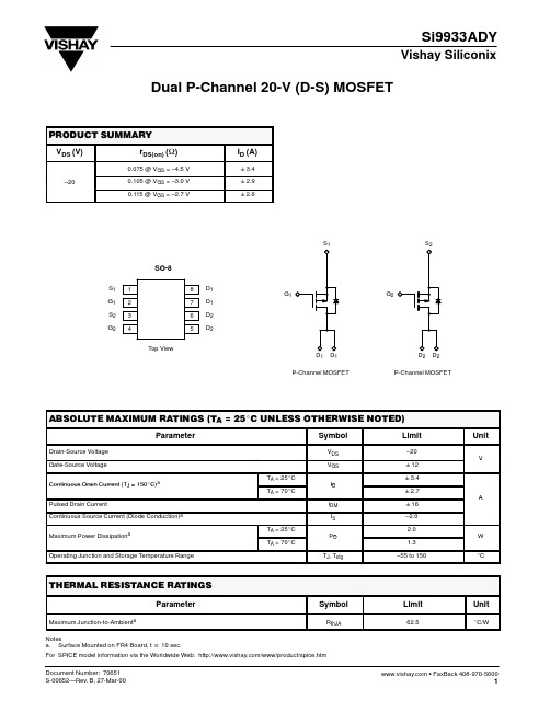
上海灿矽半导体完美替代9833D产品资料
第一功能识别位 2 无 PFC 功能
产品类别位 2 LED 驱动
公司名前缀 YT YTET
丝印命名规则
型 Y M 号 D SN
型号 日期代码
YT2207 第一引脚标识 Y:年码; M:月码; D:日码; SN:流水码
A2
8/11
YT2207_DS
封装
SOP8
符号 A A1 A2 b c D E E1 e L θ
tON
L I pk Vbus VLED
(4)
其中,VLED是LED负载的电压。 功率管关断时,电感电流下降,功率管关断时间
A2
6/11
过温调节功能
当芯片结温高于过温调节阈值( TOTR_TH )时, YT2207会通过降低输出电流Io的方式调节系统温度, 这保证了 LED 驱动芯片本身和 LED 灯珠可以同时稳定 工作,提高LED灯具系统的可靠性。图4展示了YT2207 的过温调节效果,其中 Io1为过温调节前LED驱动的输 出电流;Io2为触发过温调节后LED 驱动重新回到稳定 工作点的输出电流,此时芯片结温为Tj2。
0
t
Io1 Io2 0
Io
t
图4 YT2207过温调节效果示意
A2
7/11
YT2207_DS
型号命名规则
YT X X X X X XX 封装识别位 S8/D8 SOP8/DIP8 含铅识别位 G/* 无卤
第三功能识别位 7 功能识别补充
第二功能识别位 0 功能识别补充
毫米尺寸 最小值 最大值 1.350 1.750 0.100 0.250 1.350 1.550 0.330 0.510 0.170 0.250 4.700 5.100 3.800 4.000 5.800 6.200 1.270 (中心到中心的基本尺寸) 0.400 1.270 0º 8º
SI9933ADY中文资料
Symbol
RthJA
Limit
62.5
Unit
_C/WADY
Vishay Siliconix
SPECIFICATIONS (TJ = 25_C UNLESS OTHERWISE NOTED)
Parameter Static
Gate Threshold Voltage Gate-Body Leakage Zero Gate Voltage Drain Current VGS(th) IGSS IDSS VDS = VGS, ID = –250 mA VDS = 0 V, VGS = "12 V VDS = –16 V, VGS = 0 V VDS = –10 V, VGS = 0 V, TJ = 85_C VDS v –5 V, VGS = –4.5 V VDS v –5 V, VGS = –2.7 V VGS = –4.5 V, ID = –3.2 A Drain-Source On-State Resistanceb D i S O S R i rDS(on) VGS = –3.0 V, ID = –2.0 A VGS = –2.7 V, ID = –1 A Forward Transconductanceb Diode Forward Voltageb gfs VSD VDS = –9 V, ID = –3.4 A IS = –2.0 A, VGS = 0 V –16 A –3 0.06 0.078 0.085 8 –0.7 –1.2 0.075 0.105 0.115 S V W –0.8 "100 –1 –3 V nA mA
0.6 ID = 250 µA V GS(th) Variance (V) 0.4 Power (W) 30
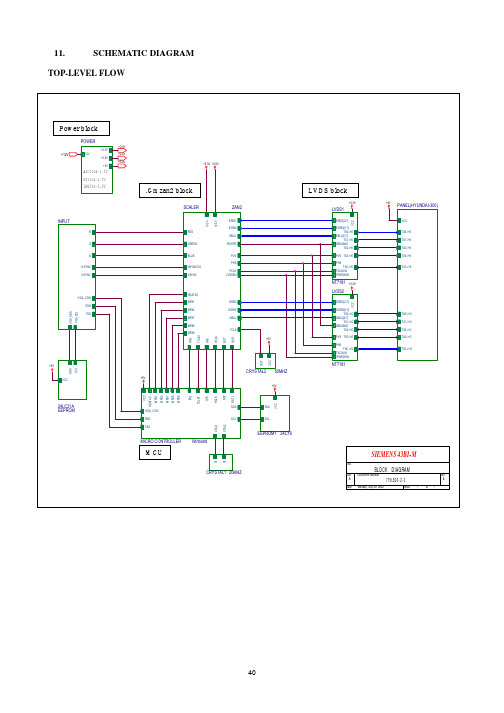
厦华液晶彩色电视机典型机芯故障检修要点
厦华液晶彩色电视机典型机芯故障检修要点(HK系列)厦华液晶彩色电视机典型机芯故障检修要点(HK系列)7.1 机型概述厦华HK系列液晶彩电是采用MST公司的主芯片为核心的系列机型.其主要机型有LC-42HK55、LC-47HK55,派生出来的机型还有LC-37HU35、LC-40HU35、LC-42HU27、LC-46HU27、LC-47HU27等.上述机型电路框架方面大致相同.7.2整机方框及接线图等7.2.1 整机的电路方框图整机的电路方框图如图7-2-1所示.图7-2-1整机的电路方框图247平板彩色电视机维修要点手册7.2.2整机的电路接线图整机的电路接线图如图7-2-2所示.7.2.3主要集成电路及其功能图7-2-2整机电路接线图①NS4(MST9U88L):它是一片全功能大规模专用集成电路,能实现HDMI接口处理、视频解码、视频开关选择、A/D和D/A变换、隔行/逐行处理、模式变换、OSD和低压差分输出处理等全部功能:另外,它还具有音频选择、处理及MCU的功能等.②NS5、NS2(24C02N-10SI27)、NS3(24C02N-10SI27):存储器,储存整机的各种重要数据.③NW200(HEF4052BT):音频信号切换/音频信号效果处理.④NA6(MP7722):伴音功放电路.⑤N512(TEA1610T):24V主开关电源控制集成电路.⑥N504(AN7809AF):9V稳压集成电路.⑦N507(A6563A):PFC控制集成电路.⑧N501(DH321):5V副电源控制集成电路.⑨N511(LM393D):过压保护电路.⑩N510(SI9933):5VSB电源控制开关.248第7章厦华液晶彩色电视机典型机芯故障检修要点(HK系列)7.3整机实际结构图解7.3.1 HK系列液晶彩电整机实际内部构造说明HK系列液晶彩电电路部分由电源板组件、数字板、高频板和转接板四大部分组成,背光板布置在屏左右两侧,键控板装置在机身的右侧,这样使得机身看上去更加简洁,这也是目前液晶电视的一种流行放置方式.接收头设置在机身的左侧.此外在细节设计方面,HK系列液晶彩电的扬声器插座还采用人性化的防呆设计,使得安装插拔更便捷,不易插错.实物图如图7-3-1所示.图7-3-1 LC42HK55内部结构图解7.3.2整机拆卸注意事项①要防ESD:CMOS和半导体器件受静电放电易损坏,操作时应将LCD组件放在防静电平台上,操作者要带防静电手环,以防静电产生.②选择合适大小的垫布:拆卸机子之前应确保选择的垫布比屏面积稍大些,以保护显示屏避免屏受到划伤.③屏线插头的插拔:HK机型的屏线插头没有用硅胶固定,拆装时需小心按下两头卡钩,以免破坏插头.④螺钉的拆卸:所有的安装孔与框架上孔的孔位应对齐,错位时支撑框架应修改,切勿249平板彩色电视机维修要点手册强行锁入螺丝.液晶电视机有规格不一、大小不一的各种螺钉,这些螺钉的安装位置都有要求,严禁装错,装错一个,如在短螺钉的地方装上长的螺钉,长的螺钉就有可能穿过安装的介体,最终顶到LCD屏上,导致LCD屏永久损坏,因此实际拆装时,不同的螺钉一定要分类摆放.⑤显示表面沾污:如果显示表面沾污,用棉签或软布擦净.如擦不净,可用棉签或软布蘸有清洗剂(挤干)擦拭.⑥异物检查:拆装结束后,应该检查有没有异物掉在机器内部,尤其是金属异物.⑦底座的拆卸:一般的机型只要拆下底座螺钉后,底座就可轻松的卸下,但是HK机型的底座设计和其他机型的不同,在底座插销壳里还设有机械卡钩,拆卸HK机型底座时,除需卸下底座螺钉外,还需拧松机身底部的4个螺钉,然后将机壳底部掰开,这时底座才拆得下来,不可生硬将底座揣出,否则会破坏底座.具体操作如图7-3-2、图7-3-3所示.图7-3-2步骤一图7-3-3步骤二7.4信号流程天线接收的射频信号RF进入高频头TUN1,经高放和混频获中频信号IF,再经VZ100预中放后送声表面波ZZ101进行中频滤波,获得较理想的中频特性,然后送入NZ100(R2S1040)进行中放、锁相环VCO及同步检波,获得全电视信号TV-CVBS;同时,IF经预中放后也送声表面波滤波器ZZ100进行滤波,再送入NZ100进行中放,输出伴音第二中频信号TV-SIF.从R2S1040输出的TV视频TV-CVBS与TV-SIF送到主芯片NS4(MST9U88L).A V1、A V2、S-VIDEO、YPbPr1和YPbPr2的视频信号也送到MST9U88L,而它们的音频信号经音频开关NW200(HEF4052BT)选择后也送到MST9U88L(其中A V1与S-VIDEO共用一组音频口).还有VGA及HDMI的视频和音频信号也都送到250第7章厦华液晶彩色电视机典型机芯故障检修要点(HK系列)MST9U88L.经MST9U88L处理的视频信号, 送出4对差分信号和1对时钟信号供液晶屏显示.而AV1、A V2、S-VIDEO和TV的视频信号经内部选择和处理后, 输出A V-OUT的视频信号,再经2倍视频放大,然后送到A V-OUT输出口.经MST9U88L处理的音频信号, 一路送到伴音功放NA6(MP7722DF), 经放大后送往喇叭; 同时, 它还送到耳机功放N350(BH3547F), 经放大后送往耳机.另外一路音频信号通过I2C总线送到D/ A转换器NS6(CS4344), 转换成模拟音频信号L/ R后送到A V-OUT输出口.7.5开关电源工作原理介绍见图7-5-1,本机电源部分由PFC部分、24V主开关电源部分、5V 电源部分、32VSC电源部分、18V电源部分、15V电源部分组成.其中,18V电源还产生18VSC 电源、9VSC电源,5V电源还产生5VSC、VSB电压.220V市电经过X501插座输入电源板,再经过RT501、C504、L501、C501、C508、C509、L503、C503、L502、C506等EMI元器件,送到整流全桥D501(D15XB60).从D501(D15XB60)的1脚输出脉动直流电, 再经PFC电感L504、PFC二极管D506到达主滤波电容C533.再到达副电源开关变压器T501的4脚,经过内部的绕组,从6脚输出到副电源控制电路N501(DH321)的6、7、8脚,在T501的1脚、3脚上互感得到的脉动电压,经R514限流、D504整流、C513滤波,提供稳定的直流电压给N501的3脚,为其提供工作电源,N501进入正常工作状态.T501的2脚绕组感应得到的脉动电压,经R516限流、D505整流、C521滤波,V501/N502稳压,得到V_15V电压.V_15V电压一路提供到N507(L6563A)的l4脚,为其供电,N507(L6563A)开始进入正常工作状态, 在13脚输出PFC驱动脉冲,控制PFC开关管V502的导通状态,PFC 电路开始工作.V_15V电压还送到N512(TEA1610T)的11脚,为其提供工作电源.N512(TEA1610T)开始工作后,在其7脚、10脚输出高低驱动脉冲,驱动24V主开关电源开关管V507(2SK3469)、V508(2SK3469),24V主开关电源开始工作.主开关电源主要产生两路24V直流电压和18V直流电压.副电源开关变压器T501的7脚绕组产生的脉动电压,经D510整流,C535滤波,V504/N509稳压,得到32V的调谐电压,送到高频头.副电源开关变压器T501的8脚绕组产生的脉动电压,经D511整流,C534/C536、L507、C539滤波,得到稳定的5V电压输出.本机24V/18V稳压控制电路是由R585、R586、R587为24V一路取样,R584、R583、R587为24V一路取样;R582、R581、R587为18V一路取样, 以及N514(TL431)稳压基准误差放大器、光耦N513(TLP421)、N512(TEA1610T)的14脚、16脚内部电阻组成.本机5V稳压控制电路是由R547、R548以及N508(TL431)稳压基准误差放大器、光耦N506(TLP421GR)、N512(TEA1510T)的3脚内部电阻组成.251252平板彩色电视机维修要点手册图7-5-1开关电源电路第7章厦华液晶彩色电视机典型机芯故障检修要点(HK系列)图7-5-1开关电源电路(续)253平板彩色电视机维修要点手册本机开关机控制信号为Standby2,是由X505的11脚输入的,Standby2信号控制主要分为3路:①Standby2控制信号经D512、R527、V503、N505控制V501的导通,从而控制了V_15V 电源的有无,从而实现对N507(L6563A)、N512(TEA1610T)两个芯片的工作电源的有无,实际上就控制了PFC电压、24V、18V电压的产生和关闭;②Standby2控制信号经R559、V506控制V504的导通和截止,从而控制了32V的产生或关闭;③Standby2控制信号经V505、R553、N510(SI9933ADY)的4脚,控制N510(SI9933ADY)的导通,从而控制5VSC电压的产生和关闭.7.6主要IC介绍7.6.1 主芯片NS4(MST9X88L)1.主芯片MST9U88L引脚图HK系列液晶彩电, 整机采用MSTAR公司的MST9X88L超级单芯片方案(内销和美洲机采用MST9U88L,欧洲机采用MST9E88L,本节主要介绍内销机),该芯片具有电路简单、接口齐全、功能强大的特点.MST9U88L集成了多路电子开关选择器、3D Decoder、10bitADC、DEINTERFACE、SCLALER、256色OSD图形、双LVDS输出、DVI/HDMI(HDCP)、3D降噪、支持SXGA/WXGA(1366x768)等功能于一体,用户界面友好.采用256脚LQFP封装(见图7-6-1),相对BGA封装具有维修方便,拆卸简单的特点.2.MST9U88L引脚说明(见表7-6-1)表7-6-1 MST9U88L引脚说明7.6.2 中放瑞萨R2S10401SP 芯片方框图1.R2S10401SP芯片引脚图(见图7-6-1)R2S10401SP最大特点是可支持多种图像格式(PAL/NTSC/SECAM)和伴音格式(DK/BG/I/M/N/L/L').254第7章厦华液晶彩色电视机典型机芯故障检修要点(HK系列)图7-6-1 R2S10401SP芯片方框图2.引脚说明(见表7-6-2)表7-6-2 引脚说明255平板彩色电视机维修要点手册7.6.3 D 类伴音功放芯片MP77221.MP7722引脚图(见图7-6-2)D类伴音功放芯片MP7722在24V供电,4Ω负载情况下,最大可以输出2x20W,无需外接散热片(底部需要和印制板保持良好焊接,以利于散热),适应宽电源9.5~26V,是MPS生产的第二代高集成音频放大芯片.它集成了以下功能:180mΩ场效应管,快速开启/关断,精简保护电路.MP7722利用一个单独的输出机构,把2x20W的功率送到4Ω的扬声器.整个电路应用了MPS自己特有的可变频率电路技术,波形失真系数小,响应时间短,单电源供电.图7-6-2引脚图2.MP7722引脚说明(见表7-6-3)表7-6-3 MP7722引脚说明256第7章厦华液晶彩色电视机典型机芯故障检修要点(HK系列)续表3.MP7722典型应用电路(见图7-6-3)图7-6-3 MP7722典型应用电路7.7工厂菜单的进入和调试方法7.7.1 工厂菜单的进入及调试方法进入工厂菜单方法:依次按"INPUT"、"2"、"5"、"8"、"0"键即可以进入工厂菜单;用"CH+"、"CH-"键选择调整项,用"VOL+"、"VOL-"键调整大小.连续按"MENU"键即可退出工厂菜单.软件升级方法:进入工厂菜单选择"OPTION"项,将ISP设为1,或者插上跳线J1,即可在线升级,升级完必须将ISP设为0或拔掉跳线J1.7.7.2初始化设置进入工厂菜单后,进入OPTION和HOTEL OPTION调整子菜单,调整项见表7-7-1.257平板彩色电视机维修要点手册表7-7-1 子菜单调整7.7.3其他调整①中放AFT调试:通电进入工厂菜单,把IF VCO调成1,或按组合键"INPUT"、"2"、"5"、"8"、"1"进入VCO调试模式,断开J2,调整LZ100使TP5(B面)的电压为2.5V,然后焊好J2.②中放AGC调试: 从RF端输入射频电视信号,调整RZ133使TP1(B面)的电压为2V,并观测画面应无明显的雪花点.再将RF端输入电视信号强度增加到90dBV,应能正常显示而无明显的网纹或噪点干扰.③出厂设置见表7-7-2.表7-7-2 出厂设置7.8维修注意事项①切勿拆卸LCD组件或者对它进行修改,以免引起电击,造成电子元器件损坏,屏表面划伤.②如自行拆卸或修改LCD屏组件,将损失LCD屏的免费保修.③当心LCD组件的破碎玻璃,注意不要造成显示屏破裂,当心割手.258第7章厦华液晶彩色电视机典型机芯故障检修要点(HK系列)④切勿碰触破裂显示屏流出的液体,假如液体溅到手脚或衣服立即用肥皂清洗或者酒精(ALCOHOL)清洗,严防液体溅入嘴、眼中,万一液体溅入眼内,应立即用大量清水冲洗至少15min,随后立即送医院.⑤LCD组件内的荧光灯含有水银,假如破碎损坏,按当地有关法规处理.⑥所有的安装孔与框架上孔的孔位应对齐,错位时支撑框架应修改,切勿强行锁入螺丝.⑦安装在LCD组件上的保险丝参数不能更改.⑧防静电.CMOSLSI和半导体器件受静电放电易损坏,操作时应将LCD组件放在防静电平台上,操作者要带防静电手环,以防静电产生.⑨显示表面沾污.如果显示表面沾污,用棉签或软布擦净.如擦不净,可用棉签或软布蘸清洗剂(挤干)擦拭;附:①理想的清洗剂:水,PA(异丙醇),Hexane[(正)己烷].②不可用的清洗剂:Ketone type(酮类),Acetone(丙酮),Ethyl alcohol(乙醇),Toluene(甲苯),Ethyl acid(乙酸),Methyl chloride(氯甲烷).它们会起化学反应而使偏光器永久性损坏.⑩操作时环境湿度:建议在50%~65%RH湿度下装配LCD组件.11储存和运输指南:不要将LCD组件储存在有有机溶剂、有腐蚀性气体的环境中.在有机溶剂环境中,偏光板会变色,显示质量下降;在腐蚀性气体环境中,各个问题都会发生.建议储存环境为:温度0~35℃,湿度50%--一65%RH.12LCD组件工作、储存环境的极限值:a.工作温度:0~50℃;b.工作湿度:20%~85%RH;C.储存温度:-20~+60℃;d.储存湿度:10%~85%RH.13液晶电视机有规格不一、大小不一的各种螺钉,这些螺钉的安装位置都有要求,严禁装错,装错一个,如在短螺钉的地方装上长的螺钉,长的螺钉就有可能穿过安装的介体,最终项到LCD屏上,导致LCD屏永久损坏,因此实际拆装时,不同的螺钉一定要分类摆放.14任何时候都不可用外力或异物去撞、划、打液晶屏.15拔插电路的有些插头时,一定要不小心,以免损坏插座或插头.16无很高的把握时,不要随意更换电路板上的任何集成电路.17拆装结束后,应该检查有没有异物掉在机器内部,尤其是金属异物.7.9 电路主要插座及主要集成电路正常工作电压7.9. 11 相关插座实测维修资料对于本节介绍的实测维修数据,电压基本上要求用数字表进行实测;接地点的选择:冷地是以LCD显示屏的金属外壳为接地点,热地以300V主滤波电容的负极为接地点;电压测量时一般用20V的量程,高于20V的用200V量程,高于200V的用1000V量程;有充放电259平板彩色电视机维修要点手册效应的引脚的电阻,必须等充放电完成后,阻值稳定下来时,再记录;把电视机置于PALD/K制,频道在1频道;并且电视机的各种模拟量,比如音量/亮度/对比度/彩色等置于适中. 对于集成电路的内部阻值来说,数据为0的那只脚就是测试时的接地脚,表笔的接地脚都是该脚.相关插座实测维修资料见表7-9-1~表7-9-12.表7-9-1 X502表7-9-2 X505表7-9-3 X506表7-9-4 X507表7-9-5 X508表7-9-6 X509表7-9-7 N102260第7章厦华液晶彩色电视机典型机芯故障检修要点(HK系列)表7-9-8 NW200表7-9-9 N103表7-9-10 N104表7-9-11 N106表7-9-12 高频头7.9.2 电源板实测维修资料电源板实测维修资料见表7-9-13~表7-9-24.表7-9-13 N501(DH321)表7-9-14 N502(TA78L09)表7-9-15 N508(TL431)表7-9-16 N510(SI9933)表7-9-17 N511(LM393D)261平板彩色电视机维修要点手册表7-9-18N512(TEAl610T)表7-9-19 N514(TL431)表7-9-20 V501(A966)表7-9-21 V502(F20W503)表7-9-22 V504(A1015)表7-9-23 V507(2SK3469)表7-9-24 V508(2SK3469)。
si3933使用手册
si3933使用手册摘要:1.Si3933 概述2.Si3933 的功能与特点3.Si3933 的应用领域4.Si3933 的使用方法与注意事项5.Si3933 的技术参数6.结论正文:Si3933 是一款高性能、低功耗的射频前端芯片,由Silicon Labs 公司设计推出。
它能够在接收器和发射器之间提供完整的射频信号处理功能,广泛应用于无线通信、物联网、智能家居等领域。
Si3933 具有以下功能与特点:首先,它支持多种调制方式,包括调幅、调频、调相等,能够满足不同应用场景的需求。
其次,Si3933 具有很高的灵敏度和选择性,能够有效地提高系统的接收性能和抗干扰能力。
此外,它还具有低功耗、小尺寸、易于集成等优点,可以大幅降低产品的开发难度和成本。
Si3933 的应用领域非常广泛,可以用于各种无线通信设备、物联网节点、智能家居控制器等。
例如,在智能家居系统中,Si3933 可以用于实现各种智能终端的联网和数据传输功能,为家庭用户带来更加便捷、舒适的生活体验。
在使用Si3933 时,需要注意以下几点:首先,要确保芯片的工作电压、电流和晶振频率等参数符合设计要求,以保证其正常工作和稳定性。
其次,在焊接芯片时,需要注意焊接温度和时间,避免对芯片造成损坏。
最后,在进行射频调试时,需要正确设置调试仪器的参数,并注意观察调试结果,以确保系统的性能达到预期。
Si3933 的技术参数包括:工作电压范围为1.8V-3.6V,工作电流为1.7mA,接收灵敏度为-104dBm,发射功率为+10dBm 等。
这些参数可以为产品设计提供重要参考。
综上所述,Si3933 是一款性能优越、应用广泛的射频前端芯片,可以为各类无线通信和物联网设备提供可靠、高效的射频信号处理功能。
SI4559ADY中文资料
VDS = – 30 V, VGS = –4.5 V, ID = –3.1 A
Qgd
Gate Resistance
Rg
f = 1 MHz
Min Typa Max Unit
N-Ch
60
V
P-Ch
–60
N-Ch
55
P-Ch
–50
mV
N-Ch
–6
P-Ch
4
N-Ch
1
P-Ch
–1
3 V
–3
ID (A)a
5.3 4.7 –3.9 –3.5
Qg (Typ)
6 nC 8nC
FEATURES D TrenchFETr Power MOSFET D 100 % Rg & UIS Tested APPLICATIONS D CCFL Inverter
RoHS
COMPLIANT
S1 1 G1 2 S2 3 G2 4
VDS Temperature Coefficient VGS(th) Temperature Coefficient Gate Threshold Voltage
DVDS/TJ DVGS(th)/TJ
VGS(th)
ID = 250 mA ID = –250 mA ID = 250 mA IID = –250 mA VDS = VGS, ID = 250 mA VDS = VGS, ID = –250 mA
P-Channel VDD = –30 V, RL = 12.5 W ID ^ –2.4 A, VGEN = –10 V, Rg =1 W
Min Typa Max Unit
N-Ch P-Ch N-Ch P-Ch N-Ch P-Ch N-Ch P-Ch N-Ch P-Ch N-Ch P-Ch N-Ch P-Ch N-Ch P-Ch
成都国盛科技有限公司 博晨(BOCHEN)3323型玻璃釉预调电位器技术承认书说明书
成都国盛科技有限公司产品品牌博晨(BOCHEN)3323型玻璃釉预调电位器技术承认书拟制:审核:批准:成都国盛科技有限公司技术质量部成都国盛科技有限公司3323型玻璃釉预调电位器技术承认书电气特性Electrical Characteristcs标称阻值范围(Range of normal resistance):50Ω—2MΩ阻值允许偏差(Resistance tolerance):±10%终端电阻(Termial resistance):≤5%R或5Ω接触电阻变化(Contact resistance variation):CRV≤5%R或5Ω耐电压(Winthstand Voltage):101.3kPa500V,8.5kPa315V绝缘电阻(Insulation resistance):Ri≥1GΩ(100Vac)有效电行程(Effective electrical travel):210°±10°环境特性Environment Characteristics额定功率(Rated Power)(315V max):0.5W70℃,0W125℃温度范围(Temperature range):-55℃~+125℃温度系数(TCR):±250ppm/℃温度变化(Temperature variation):ΔR≤±2%R,Δ(Uab/Uac)≤±1%R碰撞(Collision):390m/S2,4000cyclesΔR≤±1%R70℃电气耐久性(Electrical endurance at70℃):0.5W,1000hΔR≤±10%R 机械耐久性(Mechanical Endurance):200周(200cycles),ΔR≤±10%R恒定湿热(Steady damp-heat):ΔR≤±3%R,R1≥100MΩ物理特性Physical Characteristics总机械行程(Total Mechanical Travel):250°±10°起动力矩(Staring Torque):≤20mN.m止档力矩(Clutch Torque):≥50mN.m标准包装(Standard Packaging):50只/管(50pcs.per tube)标志(Mark):阻值允许偏差(10%不标注)、阻值代码、产品型号Resistance tolerance(when no identification,it is of±10%)resistance code type产品实物图(picture)。
矽普特产品简介
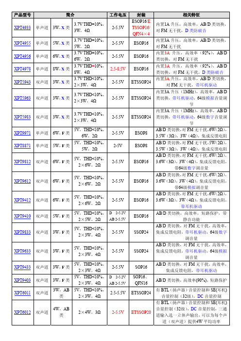
3W,AB 类 1W,AB
类
2W,AB 类
1.8W, AB 类 1W,AB
类
2.7W, AB 类 3W,AB
类 4W,AB
类
5V,THD<10%, 2.6W(ESOP8), 2.4W(SOP8),4Ω 5V,THD<10%,
2×2.6W, THD<1%,2×
1.8W,4Ω 5V,THD<10%,
产品型号 XPT4933 XPT4955 XPT4956 XPT4978 XPT5943 XPT5963
XPT5983 XPT9971 XPT8871 XPT9812
XPT9612
XPT9412 XPT9410 XPT9833
XPT9633 XPT9433 XPT9403 XPT6011
XPT6012
2-5.5V
3W,F 类
5V,THD<10%, 2×3W,4Ω
2-5.5V
3W,F 类
3W,F 类 3W,AB
类
5V,THD<10%,
2×3W,4Ω
2-5.5V
5V,THD<10%, D 2-5.2V
2×3W,4Ω AB 2-5.5V
5V,THD<10%,
2×3W,4Ω
2.5-5.5V
4W,AB 类
低电平关断,XPT4863则相反。 XPT4963完全兼容 LM4863。
单端模式,5V,THD+N≤0.5%,75mW (32Ω)。完全兼容 LM4863,CSC4863。
适用于台式、手提电脑及低压音响系统 等领域,是一款市场普遍认可并广泛采
用的典型芯片 适用于台式、手提电脑及低压音响系统 等领域,是一款市场普遍认可并广泛采
维沙伊 Siliconix S16-1757-Rev. A 汽车级N-通道80V 175°C MOS
SQJA96EP-T1_GE3SQJA96EPVishay SiliconixAutomotive N-Channel 80 V (D-S) 175 °C MOSFETFEATURES•TrenchFET ® power MOSFET •AEC-Q101 qualified •100 % R g and UIS tested•Material categorization:for definitions of compliance please see /doc?99912Notesa.Package limited.b.Pulse test; pulse width ≤ 300 μs, duty cycle ≤ 2 %.c.When mounted on 1" square PCB (FR4 material).d.See solder profile (/doc?73257). The PowerPAK SO-8L is a leadless package. The end of the lead terminal is exposed copper (not plated) as a result of the singulation process in manufacturing. A solder fillet at the exposed copper tip cannot be guaranteed and is not required to ensure adequate bottom side solder interconnection.e.Rework conditions: manual soldering with a soldering iron is not recommended for leadless components.PRODUCT SUMMARYV DS (V)80R DS(on) (Ω) at V GS = 10 V 0.0215I D (A) per leg 30Configuration Single PackagePowerPAK SO-8LPowerPAK ® S O-8L S ingle2S3S4G1SDBottom View16.15mm5.13m mTop ViewABSOLUTE MAXIMUM RATINGS (T C = 25 °C, unless otherwise noted)PARAMETER SYMBOL LIMIT UNIT Drain-Source Voltage V DS80VGate-Source Voltage V GS ± 20Continuous Drain CurrentT C = 25 °C a I D 30A T C = 125 °C19.4Continuous Source Current (Diode conduction) a I S 30Pulsed Drain Current bI DM 80Single Pulse Avalanche Current L = 0.1 mH I AS 22Single Pulse Avalanche Energy E AS 24mJ Maximum Power Dissipation bT C = 25 °C P D 48W T C = 125 °C 16Operating Junction and Storage Temperature Range T J , T stg-55 to +175°C Soldering Recommendations (Peak temperature) d, e260THERMAL RESISTANCE RATINGSPARAMETER SYMBOL LIMIT UNIT Junction-to-Ambient PCB mount cR thJA 70°C/WJunction-to-Case (Drain)R thJC3.1SQJA96EPVishay SiliconixNotesa.Pulse test; pulse width ≤ 300 μs, duty cycle ≤ 2 %.b.Guaranteed by design, not subject to production testing.c.Independent of operating temperature.Stresses beyond those listed under “Absolute Maximum Ratings” may cause permanent damage to the device. These are stress ratings only, and functional operation of the device at these or any other conditions beyond those indicated in the operational sections of the specifications is not implied. Exposure to absolute maximum rating conditions for extended periods may affect device reliability.SPECIFICATIONS (T C = 25 °C, unless otherwise noted)PARAMETER SYMBOLTEST CONDITIONS MIN.TYP.MAX.UNITStaticDrain-Source Breakdown Voltage V DS V GS = 0 V, I D = 250 μA 80--V Gate-Source Threshold Voltage V GS(th)V DS = V GS , I D = 250 μA 2.5 3.0 3.5Gate-Source LeakageI GSS V DS = 0 V, V GS = ± 20 V--± 100nAZero Gate Voltage Drain Current I DSS V GS = 0 VV DS = 80 V --1μA V GS = 0 V V DS = 80 V, T J = 125 °C --50V GS = 0 V V DS = 80 V, T J = 175 °C--150On-State Drain Current aI D(on) V GS = 10 V V DS ≥ 5 V 25--A Drain-Source On-State Resistance a R DS(on) V GS = 10 V I D = 10 A -0.01790.0215ΩV GS = 10 V I D = 10 A, T J = 125 °C --0.0353V GS = 10 VI D = 10 A, T J = 175 °C--0.0439Forward Transconductance b g fs V DS = 15 V, I D = 10 A-24-S Dynamic bInput Capacitance C issV GS = 0 V V DS = 25 V, f = 1 MHz-8751200pFOutput CapacitanceC oss -460625Reverse Transfer Capacitance C rss -2535Total Gate Charge c Q gV GS = 10 V V DS = 40 V, I D = 2.5 A -1425nC Gate-Source Charge c Q gs -4-Gate-Drain Charge c Q gd -3-Gate Resistance R g f = 1 MHz 0.180.480.75ΩTurn-On Delay Time c t d(on) V DD = 40 V, R L = 16 ΩI D ≅ 2.5 A, V GEN = 10 V, R g = 1 Ω-1325ns Rise Time ct r -310Turn-Off Delay Time c t d(off)-2140Fall Time c t f -2240Source-Drain Diode Ratin g s and Characteristics bPulsed Current a I SM --80A Forward VoltageV SDI F = 10 A, V GS = 0 V-0.861.2VOutput Characteristics Transconductance Capacitance Transfer CharacteristicsOn-Resistance vs. Drain CurrentGate Char g eOn-Resistance vs. Gate-to-Source Volta g e Threshold Volta g eDrain Source Breakdown vs. Junction TemperatureSQJA96EP Vishay SiliconixTHERMAL RATINGS(T A = 25 °C, unless otherwise noted)Safe Operatin g AreaSQJA96EP Vishay SiliconixTHERMAL RATINGS(T A = 25 °C, unless otherwise noted)Normalized Thermal Transient Impedance, Junction-to-CaseNote•The characteristics shown in the two graphs- Normalized Transient Thermal Impedance Junction-to-Ambient (25 °C)- Normalized Transient Thermal Impedance Junction-to-Case (25 °C)are given for general guidelines only to enable the user to get a “ball park” indication of part capabilities. The data are extracted from single pulse transient thermal impedance characteristics which are developed from empirical measurements. The latter is valid for the part mounted on printed circuit board - FR4, size 1" x 1" x 0.062", double sided with 2 oz. copper, 100 % on both sides. The part capabilities can widely vary depending on actual application parameters and operating conditions.Vishay Silicon ix main tain s worldwide man ufacturin g capability. Products may be man ufactured at on e of several qualified location s. Reliability data for Silicon Technology and Package Reliability represent a composite of all qualified locations. For related documents such as package/tape drawings, part marking, and reliability data, see /ppg?75618.Legal Disclaimer Notice VishayDisclaimerALL PRODUCT, PRODUCT SPECIFICAT IONS AND DAT A ARE SUBJECT T O CHANGE WIT HOUT NOT ICE T O IMPROVE RELIABILITY, FUNCTION OR DESIGN OR OTHERWISE.Vishay Intertechnology, Inc., its affiliates, agents, and employees, and all persons acting on its or their behalf (collectively, “Vishay”), disclaim any and all liability for any errors, inaccuracies or incompleteness contained in any datasheet or in any other disclosure relating to any product.Vishay makes no warranty, representation or guarantee regarding the suitability of the products for any particular purpose or the continuing production of any product. To the maximum extent permitted by applicable law, Vishay disclaims (i) any and all liability arising out of the application or use of any product, (ii) any and all liability, including without limitation special, consequential or incidental damages, and (iii) any and all implied warranties, including warranties of fitness for particular purpose, non-infringement and merchantability.Statements regarding the suitability of products for certain types of applications are based on Vishay’s knowledge of typical requirements that are often placed on Vishay products in generic applications. Such statements are not binding statements about the suitability of products for a particular application. It is the customer’s responsibility to validate that a particular product with the properties described in the product specification is suitable for use in a particular application. Parameters provided in datasheets and / or specifications may vary in different applications and performance may vary over time. All operating parameters, including typical parameters, must be validated for each customer application by the customer’s technical experts. Product specifications do not expand or otherwise modify Vishay’s terms and conditions of purchase, including but not limited to the warranty expressed therein.Except as expressly indicated in writing, Vishay products are not designed for use in medical, life-saving, or life-sustaining applications or for any other application in which the failure of the Vishay product could result in personal injury or death. Customers using or selling Vishay products not expressly indicated for use in such applications do so at their own risk. Please contact authorized Vishay personnel to obtain written terms and conditions regarding products designed for such applications.No license, express or implied, by estoppel or otherwise, to any intellectual property rights is granted by this document or by any conduct of Vishay. Product names and markings noted herein may be trademarks of their respective owners.SQJA96EP-T1_GE3。
- 1、下载文档前请自行甄别文档内容的完整性,平台不提供额外的编辑、内容补充、找答案等附加服务。
- 2、"仅部分预览"的文档,不可在线预览部分如存在完整性等问题,可反馈申请退款(可完整预览的文档不适用该条件!)。
- 3、如文档侵犯您的权益,请联系客服反馈,我们会尽快为您处理(人工客服工作时间:9:00-18:30)。
Si9933ADY
©2001 Fairchild Semiconductor International Si9933AD Y Rev A(W)
Si9933ADY
Si9933AD Y Rev A(W)
TRADEMARKS
The following are registered and unregistered trademarks Fairchild Semiconductor owns or is authorized to use and is not intended to be an exhaustive list of all such trademarks.
LIFE SUPPORT POLICY
FAIRCHILD’S PRODUCTS ARE NOT AUTHORIZED FOR USE AS CRITICAL COMPONENTS IN LIFE SUPPORT
DEVICES OR SYSTEMS WITHOUT THE EXPRESS WRITTEN APPROVAL OF FAIRCHILD SEMICONDUCTOR CORPORATION.As used herein:
1. Life support devices or systems are devices or systems which, (a) are intended for surgical implant into
the body, or (b) support or sustain life, or (c) whose
failure to perform when properly used in accordance
with instructions for use provided in the labeling, can be reasonably expected to result in significant injury to the user.
2. A critical component is any component of a life
support device or system whose failure to perform can be reasonably expected to cause the failure of the life support device or system, or to affect its safety or effectiveness.PRODUCT STATUS DEFINITIONS Definition of Terms Datasheet Identification Product Status Definition
Advance Information
Preliminary No Identification Needed Obsolete This datasheet contains the design specifications for product development. Specifications may change in any manner without notice.
This datasheet contains preliminary data, and
supplementary data will be published at a later date.Fairchild Semiconductor reserves the right to make changes at any time without notice in order to improve design.
This datasheet contains final specifications. Fairchild Semiconductor reserves the right to make changes at any time without notice in order to improve design.
This datasheet contains specifications on a product that has been discontinued by Fairchild semiconductor.The datasheet is printed for reference information only.
Formative or In Design
First Production
Full Production
Not In Production
DISCLAIMER
FAIRCHILD SEMICONDUCTOR RESERVES THE RIGHT TO MAKE CHANGES WITHOUT FURTHER NOTICE TO ANY PRODUCTS HEREIN TO IMPROVE RELIABILITY , FUNCTION OR DESIGN. FAIRCHILD DOES NOT ASSUME ANY LIABILITY ARISING OUT OF THE APPLICATION OR USE OF ANY PRODUCT OR CIRCUIT DESCRIBED HEREIN; NEITHER DOES IT CONVEY ANY LICENSE UNDER ITS PATENT RIGHTS, NOR THE RIGHTS OF OTHERS.
PowerTrench QFET™QS™
QT Optoelectronics™Quiet Series™
SILENT SWITCHER SMART START™SuperSOT™-3SuperSOT™-6SuperSOT™-8
FASTr™
GlobalOptoisolator™GTO™HiSeC™
ISOPLANAR™MICROWIRE™OPTOLOGIC™OPTOPLANAR™PACMAN™POP™
Rev. G
ACEx™
Bottomless™CoolFET™
CROSSVOLT ™DOME™E 2CMOS TM EnSigna TM FACT™
FACT Quiet Series™FAST SyncFET™TinyLogic™UHC™VCX™。