MAX4051AEEE+中文资料
MAX13085EESA-T中文资料

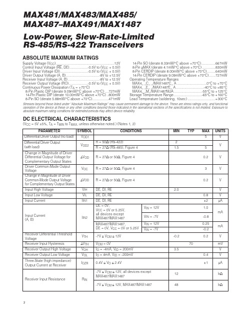
General DescriptionThe MAX13080E–MAX13089E +5.0V, ±15kV ESD-protect-ed, RS-485/RS-422 transceivers feature one driver and one receiver. These devices include fail-safe circuitry,guaranteeing a logic-high receiver output when receiver inputs are open or shorted. The receiver outputs a logic-high if all transmitters on a terminated bus are disabled (high impedance). The MAX13080E–MAX13089E include a hot-swap capability to eliminate false transitions on the bus during power-up or hot insertion.The MAX13080E/MAX13081E/MAX13082E feature reduced slew-rate drivers that minimize EMI and reduce reflections caused by improperly terminated cables, allowing error-free data transmission up to 250kbps. The MAX13083E/MAX13084E/MAX13085E also feature slew-rate-limited drivers but allow transmit speeds up to 500kbps. The MAX13086E/MAX13087E/MAX13088E driver slew rates are not limited, making transmit speeds up to 16Mbps possible. The MAX13089E slew rate is pin selectable for 250kbps,500kbps, and 16Mbps.The MAX13082E/MAX13085E/MAX13088E are intended for half-duplex communications, and the MAX13080E/MAX13081E/MAX13083E/MAX13084E/MAX13086E/MAX13087E are intended for full-duplex communica-tions. The MAX13089E is selectable for half-duplex or full-duplex operation. It also features independently programmable receiver and transmitter output phase through separate pins.The MAX13080E–MAX13089E transceivers draw 1.2mA of supply current when unloaded or when fully loaded with the drivers disabled. All devices have a 1/8-unit load receiver input impedance, allowing up to 256transceivers on the bus.The MAX13080E/MAX13083E/MAX13086E/MAX13089E are available in 14-pin PDIP and 14-pin SO packages.The MAX13081E/MAX13082E/MAX13084E/MAX13085E/MAX13087E/MAX13088E are available in 8-pin PDIP and 8-pin SO packages. The devices operate over the com-mercial, extended, and automotive temperature ranges.ApplicationsUtility Meters Lighting Systems Industrial Control Telecom Security Systems Instrumentation ProfibusFeatures♦+5.0V Operation♦Extended ESD Protection for RS-485/RS-422 I/O Pins±15kV Human Body Model ♦True Fail-Safe Receiver While Maintaining EIA/TIA-485 Compatibility ♦Hot-Swap Input Structures on DE and RE ♦Enhanced Slew-Rate Limiting Facilitates Error-Free Data Transmission(MAX13080E–MAX13085E/MAX13089E)♦Low-Current Shutdown Mode (Except MAX13081E/MAX13084E/MAX13087E)♦Pin-Selectable Full-/Half-Duplex Operation (MAX13089E)♦Phase Controls to Correct for Twisted-Pair Reversal (MAX13089E)♦Allow Up to 256 Transceivers on the Bus ♦Available in Industry-Standard 8-Pin SO PackageMAX13080E–MAX13089E+5.0V , ±15kV ESD-Protected, Fail-Safe, Hot-Swap, RS-485/RS-422 Transceivers________________________________________________________________Maxim Integrated Products 1Ordering Information19-3590; Rev 1; 4/05For pricing, delivery, and ordering information,please contact Maxim/Dallas Direct!at 1-888-629-4642, or visit Maxim’s website at .Selector Guide, Pin Configurations, and Typical Operating Circuits appear at end of data sheet.Ordering Information continued at end of data sheet.M A X 13080E –M A X 13089E+5.0V , ±15kV ESD-Protected, Fail-Safe, Hot-Swap, RS-485/RS-422 Transceivers 2_______________________________________________________________________________________ABSOLUTE MAXIMUM RATINGSDC ELECTRICAL CHARACTERISTICS(V CC = +5.0V ±10%, T A = T MIN to T MAX , unless otherwise noted. Typical values are at V CC = +5.0V and T A = +25°C.) (Note 1)Stresses beyond those listed under “Absolute Maximum Ratings” may cause permanent damage to the device. These are stress ratings only, and functional operation of the device at these or any other conditions beyond those indicated in the operational sections of the specifications is not implied. Exposure to absolute maximum rating conditions for extended periods may affect device reliability.(All Voltages Referenced to GND)Supply Voltage (V CC ).............................................................+6V Control Input Voltage (RE , DE, SLR,H/F , TXP, RXP)......................................................-0.3V to +6V Driver Input Voltage (DI)...........................................-0.3V to +6V Driver Output Voltage (Z, Y, A, B).............................-8V to +13V Receiver Input Voltage (A, B)....................................-8V to +13V Receiver Input VoltageFull Duplex (A, B)..................................................-8V to +13V Receiver Output Voltage (RO)....................-0.3V to (V CC + 0.3V)Driver Output Current.....................................................±250mAContinuous Power Dissipation (T A = +70°C)8-Pin SO (derate 5.88mW/°C above +70°C).................471mW 8-Pin Plastic DIP (derate 9.09mW/°C above +70°C).....727mW 14-Pin SO (derate 8.33mW/°C above +70°C)...............667mW 14-Pin Plastic DIP (derate 10.0mW/°C above +70°C)...800mW Operating Temperature RangesMAX1308_EC_ _.................................................0°C to +75°C MAX1308_EE_ _..............................................-40°C to +85°C MAX1308_EA_ _............................................-40°C to +125°C Junction Temperature......................................................+150°C Storage Temperature Range.............................-65°C to +150°C Lead Temperature (soldering, 10s).................................+300°CMAX13080E–MAX13089E+5.0V , ±15kV ESD-Protected, Fail-Safe, Hot-Swap, RS-485/RS-422 Transceivers_______________________________________________________________________________________3DC ELECTRICAL CHARACTERISTICS (continued)(V CC = +5.0V ±10%, T A = T MIN to T MAX , unless otherwise noted. Typical values are at V CC = +5.0V and T A = +25°C.) (Note 1)M A X 13080E –M A X 13089E+5.0V , ±15kV ESD-Protected, Fail-Safe, Hot-Swap, RS-485/RS-422 Transceivers 4_______________________________________________________________________________________DRIVER SWITCHING CHARACTERISTICSMAX13080E/MAX13081E/MAX13082E/MAX13089E WITH SRL = UNCONNECTED (250kbps)(V CC = +5.0V ±10%, T A = T MIN to T MAX , unless otherwise noted. Typical values are at V CC = +5.0V and T A = +25°C.)RECEIVER SWITCHING CHARACTERISTICSMAX13080E/MAX13081E/MAX13082E/MAX13089E WITH SRL = UNCONNECTED (250kbps)(V CC = +5.0V ±10%, T A = T MIN to T MAX , unless otherwise noted. Typical values are at V CC = +5.0V and T A = +25°C.)MAX13080E–MAX13089E+5.0V , ±15kV ESD-Protected, Fail-Safe, Hot-Swap, RS-485/RS-422 Transceivers_______________________________________________________________________________________5DRIVER SWITCHING CHARACTERISTICSMAX13083E/MAX13084E/MAX13085E/MAX13089E WITH SRL = V CC (500kbps)(V CC = +5.0V ±10%, T A = T MIN to T MAX , unless otherwise noted. Typical values are at V CC = +5.0V and T A = +25°C.)RECEIVER SWITCHING CHARACTERISTICSMAX13083E/MAX13084E/MAX13085E/MAX13089E WITH SRL = V CC (500kbps)(V CC = +5.0V ±10%, T A = T MIN to T MAX , unless otherwise noted. Typical values are at V CC = +5.0V and T A = +25°C.)M A X 13080E –M A X 13089E+5.0V , ±15kV ESD-Protected, Fail-Safe, Hot-Swap, RS-485/RS-422 Transceivers 6_______________________________________________________________________________________DRIVER SWITCHING CHARACTERISTICSMAX13086E/MAX13087E/MAX13088E/MAX13089E WITH SRL = GND (16Mbps)(V CC = +5.0V ±10%, T A = T MIN to T MAX , unless otherwise noted. Typical values are at V CC = +5.0V and T A = +25°C.)RECEIVER SWITCHING CHARACTERISTICSMAX13086E/MAX13087E/MAX13088E/MAX13089E WITH SRL = GND (16Mbps)(V CC = +5.0V ±10%, T A = T MIN to T MAX , unless otherwise noted. Typical values are at V CC = +5.0V and T A = +25°C.)Note 2:∆V OD and ∆V OC are the changes in V OD and V OC , respectively, when the DI input changes state.Note 3:The short-circuit output current applies to peak current just prior to foldback current limiting. The short-circuit foldback outputcurrent applies during current limiting to allow a recovery from bus contention.MAX13080E–MAX13089E+5.0V , ±15kV ESD-Protected, Fail-Safe, Hot-Swap, RS-485/RS-422 Transceivers_______________________________________________________________________________________70.800.901.501.101.001.201.301.401.60-40-10520-253550958011065125SUPPLY CURRENT vs. TEMPERATURETEMPERATURE (°C)S U P P L Y C U R R E N T (m A )0201040305060021345OUTPUT CURRENTvs. RECEIVER OUTPUT-HIGH VOLTAGEM A X 13080E -89E t o c 02OUTPUT HIGH VOLTAGE (V)O U T P U T C U R R E N T (m A )20104030605070021345OUTPUT CURRENTvs. RECEIVER OUTPUT-LOW VOLTAGEM A X 13080E -89E t o c 03OUTPUT LOW VOLTAGE (V)O U T P U T C U R R E N T (m A )4.04.44.24.84.65.25.05.4RECEIVER OUTPUT-HIGH VOLTAGEvs. TEMPERATURETEMPERATURE (°C)O U T P U T H I G H V O L T A G E (V )-40-10520-2535509580110651250.10.70.30.20.40.50.60.8RECEIVER OUTPUT-LOW VOLTAGEvs. TEMPERATURETEMPERATURE (°C)O U T P U T L O W V O L T A G E (V )-40-10520-25355095801106512502040608010012014016012345DRIVER DIFFERENTIAL OUTPUT CURRENT vs. DIFFERENTIAL OUTPUT VOLTAGEDIFFERENTIAL OUTPUT VOLTAGE (V)D I F FE R E N T I A L O U T P U T C U R R E N T (m A )2.02.82.43.63.24.44.04.8DRIVER DIFFERENTIAL OUTPUT VOLTAGE vs. TEMPERATURED I F FE R E N T I A L O U T P U T V O L T A G E (V )-40-10520-253550958011065125TEMPERATURE (°C)40201008060120140180160200-7-5-4-6-3-2-1012354OUTPUT CURRENT vs. TRANSMITTEROUTPUT-HIGH VOLTAGEOUTPUT HIGH VOLTAGE (V)O U T P U T C U R R E N T (m A )60402080100120140160180200042681012OUTPUT CURRENT vs. TRANSMITTEROUTPUT-LOW VOLTAGEOUTPUT-LOW VOLTAGE (V)O U T P U T C U R R E N T (m A )Typical Operating Characteristics(V CC = +5.0V, T A = +25°C, unless otherwise noted.)M A X 13080E –M A X 13089E+5.0V , ±15kV ESD-Protected, Fail-Safe, Hot-Swap, RS-485/RS-422 Transceivers 8_______________________________________________________________________________________21543679810SHUTDOWN CURRENT vs. TEMPERATUREM A X 13080E -89E t o c 10S H U T D O W N C U R R E N T (µA )-40-10520-253550958011065125TEMPERATURE (°C)600800700100090011001200DRIVER PROPAGATION DELAY vs. TEMPERATURE (250kbps)D R I VE R P R O P A G A T I O N D E L A Y (n s )-40-10520-253550958011065125TEMPERATURE (°C)300400350500450550600DRIVER PROPAGATION DELAY vs. TEMPERATURE (500kbps)D R I VE R P R O P A G A T I O N D E L A Y (n s )-40-10520-253550958011065125TEMPERATURE (°C)1070302040506080DRIVER PROPAGATION DELAY vs. TEMPERATURE (16Mbps)D R I VE R P R O P A G A T I O N D E L A Y (n s )-40-10520-253550958011065125TEMPERATURE (°C)40201008060120140160180RECEIVER PROPAGATION DELAYvs. TEMPERATURE (250kpbs AND 500kbps)R E C E I V E R P R O P A G A T I O N D E L A Y (n s )-40-10520-253550958011065125TEMPERATURE (°C)40201008060120140160180RECEIVER PROPAGATION DELAYvs. TEMPERATURE (16Mbps)R EC E I V E R P R O P A G AT I O N D E L A Y (n s )-40-10520-253550958011065125TEMPERATURE (°C)2µs/div DRIVER PROPAGATION DELAY (250kbps)DI 2V/divV Y - V Z 5V/divR L = 100Ω200ns/divRECEIVER PROPAGATION DELAY(250kbps AND 500kbps)V A - V B 5V/divRO 2V/divTypical Operating Characteristics (continued)(V CC = +5.0V, T A = +25°C, unless otherwise noted.)MAX13080E–MAX13089E+5.0V , ±15kV ESD-Protected, Fail-Safe, Hot-Swap, RS-485/RS-422 Transceivers_______________________________________________________________________________________9Test Circuits and Waveforms400ns/divDRIVER PROPAGATION DELAY (500kbps)DI 2V/divR L = 100ΩV Y - V Z 5V/div10ns/div DRIVER PROPAGATION DELAY (16Mbps)DI 2V/divR L = 100ΩV Y 2V/divV Z 2V/div40ns/divRECEIVER PROPAGATION DELAY (16Mbps)V B 2V/divR L = 100ΩRO 2V/divV A 2V/divTypical Operating Characteristics (continued)(V CC = +5.0V, T A = +25°C, unless otherwise noted.)Figure 2. Driver Timing Test CircuitM A X 13080E –M A X 13089E+5.0V , ±15kV ESD-Protected, Fail-Safe, Hot-Swap, RS-485/RS-422 Transceivers 10______________________________________________________________________________________Test Circuits and Waveforms (continued)Figure 4. Driver Enable and Disable Times (t DHZ , t DZH , t DZH(SHDN))DZL DLZ DLZ(SHDN)MAX13080E–MAX13089E+5.0V , ±15kV ESD-Protected, Fail-Safe, Hot-Swap, RS-485/RS-422 TransceiversTest Circuits and Waveforms (continued)Figure 6. Receiver Propagation Delay Test CircuitM A X 13080E –M A X 13089E+5.0V , ±15kV ESD-Protected, Fail-Safe, Hot-Swap, RS-485/RS-422 TransceiversMAX13080E–MAX13089E+5.0V , ±15kV ESD-Protected, Fail-Safe, Hot-Swap, RS-485/RS-422 TransceiversMAX13080E/MAX13083E/MAX13086EMAX13081E/MAX13084E/MAX13086E/MAX13087EFunction TablesM A X 13080E –M A X 13089E+5.0V , ±15kV ESD-Protected, Fail-Safe, Hot-Swap, RS-485/RS-422 Transceivers MAX13082E/MAX13085E/MAX13088EFunction Tables (continued)MAX13089EDetailed Description The MAX13080E–MAX13089E high-speed transceivers for RS-485/RS-422 communication contain one driver and one receiver. These devices feature fail-safe circuit-ry, which guarantees a logic-high receiver output when the receiver inputs are open or shorted, or when they are connected to a terminated transmission line with all dri-vers disabled (see the Fail-Safe section). The MAX13080E/MAX13082E/MAX13083E/MAX13085E/ MAX13086E/MAX13088E/MAX13089E also feature a hot-swap capability allowing line insertion without erroneous data transfer (see the Hot Swap Capability section). The MAX13080E/MAX13081E/MAX13082E feature reduced slew-rate drivers that minimize EMI and reduce reflec-tions caused by improperly terminated cables, allowing error-free data transmission up to 250kbps. The MAX13083E/MAX13084E/MAX13085E also offer slew-rate limits allowing transmit speeds up to 500kbps. The MAX13086E/MAX13087E/MAX13088Es’ driver slew rates are not limited, making transmit speeds up to 16Mbps possible. The MAX13089E’s slew rate is selectable between 250kbps, 500kbps, and 16Mbps by driving a selector pin with a three-state driver.The MAX13082E/MAX13085E/MAX13088E are half-duplex transceivers, while the MAX13080E/MAX13081E/ MAX13083E/MAX13084E/MAX13086E/MAX13087E are full-duplex transceivers. The MAX13089E is selectable between half- and full-duplex communication by driving a selector pin (H/F) high or low, respectively.All devices operate from a single +5.0V supply. Drivers are output short-circuit current limited. Thermal-shutdown circuitry protects drivers against excessive power dissi-pation. When activated, the thermal-shutdown circuitry places the driver outputs into a high-impedance state.Receiver Input Filtering The receivers of the MAX13080E–MAX13085E, and the MAX13089E when operating in 250kbps or 500kbps mode, incorporate input filtering in addition to input hysteresis. This filtering enhances noise immunity with differential signals that have very slow rise and fall times. Receiver propagation delay increases by 25% due to this filtering.Fail-Safe The MAX13080E family guarantees a logic-high receiver output when the receiver inputs are shorted or open, or when they are connected to a terminated transmission line with all drivers disabled. This is done by setting the receiver input threshold between -50mV and -200mV. If the differential receiver input voltage (A - B) is greater than or equal to -50mV, RO is logic-high. If (A - B) is less than or equal to -200mV, RO is logic-low. In the case of a terminated bus with all transmitters disabled, the receiv-er’s differential input voltage is pulled to 0V by the termi-nation. With the receiver thresholds of the MAX13080E family, this results in a logic-high with a 50mV minimumnoise margin. Unlike previous fail-safe devices, the-50mV to -200mV threshold complies with the ±200mVEIA/TIA-485 standard.Hot-Swap Capability (Except MAX13081E/MAX13084E/MAX13087E)Hot-Swap InputsWhen circuit boards are inserted into a hot or powered backplane, differential disturbances to the data buscan lead to data errors. Upon initial circuit board inser-tion, the data communication processor undergoes itsown power-up sequence. During this period, the processor’s logic-output drivers are high impedanceand are unable to drive the DE and RE inputs of these devices to a defined logic level. Leakage currents up to±10µA from the high-impedance state of the proces-sor’s logic drivers could cause standard CMOS enableinputs of a transceiver to drift to an incorrect logic level. Additionally, parasitic circuit board capacitance couldcause coupling of V CC or GND to the enable inputs. Without the hot-swap capability, these factors could improperly enable the transceiver’s driver or receiver.When V CC rises, an internal pulldown circuit holds DElow and RE high. After the initial power-up sequence,the pulldown circuit becomes transparent, resetting thehot-swap tolerable input.Hot-Swap Input CircuitryThe enable inputs feature hot-swap capability. At theinput there are two NMOS devices, M1 and M2 (Figure 9). When V CC ramps from zero, an internal 7µstimer turns on M2 and sets the SR latch, which alsoturns on M1. Transistors M2, a 1.5mA current sink, andM1, a 500µA current sink, pull DE to GND through a5kΩresistor. M2 is designed to pull DE to the disabledstate against an external parasitic capacitance up to100pF that can drive DE high. After 7µs, the timer deactivates M2 while M1 remains on, holding DE low against three-state leakages that can drive DE high. M1 remains on until an external source overcomes the required input current. At this time, the SR latch resetsand M1 turns off. When M1 turns off, DE reverts to a standard, high-impedance CMOS input. Whenever V CCdrops below 1V, the hot-swap input is reset.For RE there is a complementary circuit employing two PMOS devices pulling RE to V CC. MAX13080E–MAX13089E+5.0V, ±15kV ESD-Protected, Fail-Safe, Hot-Swap, RS-485/RS-422 TransceiversM A X 13080E –M A X 13089EMAX13089E ProgrammingThe MAX13089E has several programmable operating modes. Transmitter rise and fall times are programma-ble, resulting in maximum data rates of 250kbps,500kbps, and 16Mbps. To select the desired data rate,drive SRL to one of three possible states by using a three-state driver: V CC , GND, or unconnected. F or 250kbps operation, set the three-state device in high-impedance mode or leave SRL unconnected. F or 500kbps operation, drive SRL high or connect it to V CC .F or 16Mbps operation, drive SRL low or connect it to GND. SRL can be changed during operation without interrupting data communications.Occasionally, twisted-pair lines are connected backward from normal orientation. The MAX13089E has two pins that invert the phase of the driver and the receiver to cor-rect this problem. F or normal operation, drive TXP and RXP low, connect them to ground, or leave them uncon-nected (internal pulldown). To invert the driver phase,drive TXP high or connect it to V CC . To invert the receiver phase, drive RXP high or connect it to V CC . Note that the receiver threshold is positive when RXP is high.The MAX13089E can operate in full- or half-duplex mode. Drive H/F low, leave it unconnected (internal pulldown), or connect it to GND for full-duplex opera-tion. Drive H/F high for half-duplex operation. In full-duplex mode, the pin configuration of the driver and receiver is the same as that of a MAX13080E. In half-duplex mode, the receiver inputs are internally connect-ed to the driver outputs through a resistor-divider. This effectively changes the function of the device’s outputs.Y becomes the noninverting driver output and receiver input, Z becomes the inverting driver output and receiver input. In half-duplex mode, A and B are still connected to ground through an internal resistor-divider but they are not internally connected to the receiver.±15kV ESD ProtectionAs with all Maxim devices, ESD-protection structures are incorporated on all pins to protect against electro-static discharges encountered during handling and assembly. The driver outputs and receiver inputs of the MAX13080E family of devices have extra protection against static electricity. Maxim’s engineers have devel-oped state-of-the-art structures to protect these pins against ESD of ±15kV without damage. The ESD struc-tures withstand high ESD in all states: normal operation,shutdown, and powered down. After an ESD event, the MAX13080E–MAX13089E keep working without latchup or damage.ESD protection can be tested in various ways. The transmitter outputs and receiver inputs of the MAX13080E–MAX13089E are characterized for protec-tion to the following limits:•±15kV using the Human Body Model•±6kV using the Contact Discharge method specified in IEC 61000-4-2ESD Test ConditionsESD performance depends on a variety of conditions.Contact Maxim for a reliability report that documents test setup, test methodology, and test results.Human Body ModelFigure 10a shows the Human Body Model, and Figure 10b shows the current waveform it generates when dis-charged into a low impedance. This model consists of a 100pF capacitor charged to the ESD voltage of interest,which is then discharged into the test device through a 1.5k Ωresistor.IEC 61000-4-2The IEC 61000-4-2 standard covers ESD testing and performance of finished equipment. However, it does not specifically refer to integrated circuits. The MAX13080E family of devices helps you design equip-ment to meet IEC 61000-4-2, without the need for addi-tional ESD-protection components.+5.0V , ±15kV ESD-Protected, Fail-Safe, Hot-Swap, RS-485/RS-422 TransceiversThe major difference between tests done using the Human Body Model and IEC 61000-4-2 is higher peak current in IEC 61000-4-2 because series resistance is lower in the IEC 61000-4-2 model. Hence, the ESD with-stand voltage measured to IEC 61000-4-2 is generally lower than that measured using the Human Body Model. Figure 10c shows the IEC 61000-4-2 model, and Figure 10d shows the current waveform for IEC 61000-4-2 ESD Contact Discharge test.Machine Model The machine model for ESD tests all pins using a 200pF storage capacitor and zero discharge resis-tance. The objective is to emulate the stress caused when I/O pins are contacted by handling equipment during test and assembly. Of course, all pins require this protection, not just RS-485 inputs and outputs.Applications Information256 Transceivers on the BusThe standard RS-485 receiver input impedance is 12kΩ(1-unit load), and the standard driver can drive up to 32-unit loads. The MAX13080E family of transceivers has a1/8-unit load receiver input impedance (96kΩ), allowingup to 256 transceivers to be connected in parallel on one communication line. Any combination of these devices,as well as other RS-485 transceivers with a total of 32-unit loads or fewer, can be connected to the line.Reduced EMI and ReflectionsThe MAX13080E/MAX13081E/MAX13082E feature reduced slew-rate drivers that minimize EMI and reduce reflections caused by improperly terminated cables, allowing error-free data transmission up to250kbps. The MAX13083E/MAX13084E/MAX13085Eoffer higher driver output slew-rate limits, allowing transmit speeds up to 500kbps. The MAX13089E withSRL = V CC or unconnected are slew-rate limited. WithSRL unconnected, the MAX13089E error-free data transmission is up to 250kbps. With SRL connected toV CC,the data transmit speeds up to 500kbps. MAX13080E–MAX13089E+5.0V, ±15kV ESD-Protected, Fail-Safe, Hot-Swap, RS-485/RS-422 TransceiversM A X 13080E –M A X 13089ELow-Power Shutdown Mode (Except MAX13081E/MAX13084E/MAX13087E)Low-power shutdown mode is initiated by bringing both RE high and DE low. In shutdown, the devices typically draw only 2.8µA of supply current.RE and DE can be driven simultaneously; the devices are guaranteed not to enter shutdown if RE is high and DE is low for less than 50ns. If the inputs are in this state for at least 700ns, the devices are guaranteed to enter shutdown.Enable times t ZH and t ZL (see the Switching Characteristics section) assume the devices were not in a low-power shutdown state. Enable times t ZH(SHDN)and t ZL(SHDN)assume the devices were in shutdown state. It takes drivers and receivers longer to become enabled from low-power shutdown mode (t ZH(SHDN), t ZL(SHDN))than from driver/receiver-disable mode (t ZH , t ZL ).Driver Output ProtectionTwo mechanisms prevent excessive output current and power dissipation caused by faults or by bus contention.The first, a foldback current limit on the output stage,provides immediate protection against short circuits over the whole common-mode voltage range (see the Typical Operating Characteristics ). The second, a thermal-shut-down circuit, forces the driver outputs into a high-imped-ance state if the die temperature exceeds +175°C (typ).Line LengthThe RS-485/RS-422 standard covers line lengths up to 4000ft. F or line lengths greater than 4000ft, use the repeater application shown in Figure 11.Typical ApplicationsThe MAX13082E/MAX13085E/MAX13088E/MAX13089E transceivers are designed for bidirectional data commu-nications on multipoint bus transmission lines. F igures 12 and 13 show typical network applications circuits. To minimize reflections, terminate the line at both ends in its characteristic impedance, and keep stub lengths off the main line as short as possible. The slew-rate-lim-ited MAX13082E/MAX13085E and the two modes of the MAX13089E are more tolerant of imperfect termination.Chip InformationTRANSISTOR COUNT: 1228PROCESS: BiCMOS+5.0V , ±15kV ESD-Protected, Fail-Safe, Hot-Swap, RS-485/RS-422 TransceiversFigure 11. Line Repeater for MAX13080E/MAX13081E/MAX13083E/MAX13084E/MAX13086E/MAX13087E/MAX13089E in Full-Duplex Mode+5.0V, ±15kV ESD-Protected, Fail-Safe, Hot-Swap, RS-485/RS-422 TransceiversMAX13080E–MAX13089EM A X 13080E –M A X 13089E+5.0V , ±15kV ESD-Protected, Fail-Safe, Hot-Swap, RS-485/RS-422 TransceiversPin Configurations and Typical Operating CircuitsMAX13080E–MAX13089E+5.0V , ±15kV ESD-Protected, Fail-Safe, Hot-Swap, RS-485/RS-422 Transceivers______________________________________________________________________________________21Pin Configurations and Typical Operating Circuits (continued)M A X 13080E –M A X 13089E+5.0V , ±15kV ESD-Protected, Fail-Safe, Hot-Swap, RS-485/RS-422 Transceivers 22______________________________________________________________________________________Ordering Information (continued)MAX13080E–MAX13089E+5.0V , ±15kV ESD-Protected, Fail-Safe, Hot-Swap, RS-485/RS-422 Transceivers______________________________________________________________________________________23Package Information (continued)(The package drawing(s) in this data sheet may not reflect the most current specifications. For the latest package outline information,go to /packages .)。
MEMORY存储芯片MAX4051ACSE中文规格书

(V CC = +3.3V, T A = +25°C)Note 1: ∆V OD and ∆V OC are the changes in V OD and V OC , respectively, when the DI input changes state.Note 2: Measured on |t PLH (Y) - t PHL (Y)| and |t PLH (Z) - t PHL (Z)|.Note 3: The transceivers are put into shutdown by bringing RE high and DE low. If the inputs are in this state for less than 80ns, the parts are guaranteed not to enter shutdown. If the inputs are in this state for at least 300ns, the parts are guaranteed tohave entered shutdown. See Low-Power Shutdown Mode section.PARAMETERSYMBOL CONDITIONS MIN TYP MAX UNITS Time to Shutdownt SHDN MAX3483E/MAX3485E/MAX3486E/MAX3491E only (Note 3)80190300ns Receiver Propagation Delay,Low-to-High Levelt RPLH V ID = 0 to 3.0, C L = 15pF, Figure 11256290ns MAX3483E/MAX3488E 2575120Receiver Propagation Delay,High-to-Low Levelt RPHL V ID = 0 to 3.0, C L = 15pF, Figure 11256290ns MAX3483E/MAX3488E 2575120|t PLH - t PHL | ReceiverPropagation Delay Skewt RPDS V ID = 0 to 3.0, C L = 15pF, Figure 116±10ns MAX3483E/MAX3488E 12±20Receiver Output Enable Timeto Low Levelt PRZL C L = 15pF, Figure 12,MAX3483E/85E/86E/91E only 2550ns Receiver Output Enable Timeto High Levelt PRZH C L = 15pF, Figure 12,MAX3483E/85E/86E/91E only 2550ns Receiver Output DisableTime from High Levelt PRHZ C L = 15pF, Figure 12,MAX3483E/85E/86E/91E only 2545ns Receiver Output DisableTime from Low Levelt PRLZ C L = 15pF, Figure 12,MAX3483E/85E/86E/91E only 2545ns Receiver Output Enable Timefrom Shutdown to Low Levelt PRSL C L = 15pF, Figure 12,MAX3483E/85E/86E/91E only 7201400ns Receiver Output Enable Timefrom Shutdown to High Level t PRSH C L = 15pF, Figure 12,MAX3483E/85E/86E/91E only 7201400nsMAX3483E/MAX3485E/MAX3486E/MAX3488E/MAX3490E/MAX3491E3.3V-Powered, ±15kV ESD-Protected, 12Mbps and Slew-Rate-Limited True RS-485/RS-422 Transceivers Receiver Switching CharacteristicsGeneral DescriptionDevices in the MAX3483E family (MAX3483E/MAX3485E/MAX3486E/MAX3488E/MAX3490E/MAX3491E) are ±15kV ESD-protected, +3.3V, low-power transceivers for RS-485 and RS-422 communications. Each device con-tains one driver and one receiver. The MAX3483E and MAX3488E feature slew-rate-limited drivers that minimize EMI and reduce reflections caused by improperly termi-nated cables, allowing error-free data transmission at data rates up to 250kbps. The partially slew-rate-limited MAX3486E transmits up to 2.5Mbps. The MAX3485E, MAX3490E, and MAX3491E transmit at up to 12Mbps.All devices feature enhanced electrostatic discharge (ESD) protection. All transmitter outputs and receiver inputs are protected to ±15kV using IEC 1000-4-2 Air-Gap Discharge, ±8kV using IEC 1000-4-2 Contact Discharge, and ±15kV using the Human Body Model.Drivers are short-circuit current limited and are protected against excessive power dissipation by thermal shutdown circuitry that places the driver outputs into a high-impedance state. The receiver input has a fail-safe feature that guar-antees a logic-high output if both inputs are open circuit.The MAX3488E, MAX3490E, and MAX3491E feature full-duplex communication, while the MAX3483E, MAX3485E, and MAX3486E are designed for half-duplex communication.Applications ●Telecommunications ●Industrial-Control Local Area Networks ●Transceivers for EMI-Sensitive Applications ●Integrated Services Digital Networks ●Packet Switching Features ●ESD Protection for RS-485 I/O Pins •±15kV—Human Body Model •±8kV—IEC 1000-4-2, Contact Discharge •±15kV—IEC 1000-4-2, Air-Gap Discharge ●Operate from a Single +3.3V Supply—No Charge Pump Required ●Interoperable with +5V Logic ●Guaranteed 12Mbps Data Rate (MAX3485E/MAX3490E/MAX3491E)●Slew-Rate Limited for Errorless Data Transmission (MAX3483E/MAX3488E)●2nA Low-Current Shutdown Mode (MAX3483E/MAX3485E/MAX3486E/MAX3491E)●-7V to +12V Common-Mode Input Voltage Range ●Full-Duplex and Half-Duplex Versions Available ●Industry-Standard 75176 Pinout (MAX3483E/MAX3485E/MAX3486E)●Current-Limiting and Thermal Shutdown for Driver Overload Protection Ordering Information continued at end of data sheet.PARTTEMP . RANGE PIN-PACKAGE MAX3483E CSA0°C to+70°C 8 SO MAX3483ECPA0°C to+70°C 8 Plastic DIP MAX3483EESA-40°C to+85°C 8 SO MAX3483EEPA -40°C to+85°C 8 Plastic DIP PART NUMBERGUARANTEED DATA RATE (Mbps)SUPPLY VOLTAGE (V)HALF/FULL DUPLEX SLEW-RATE LIMITED DRIVER/RECEIVER ENABLE SHUTDOWN CURRENT (nA)±15kV ESD PROTECTION PIN COUNT MAX3483E0.25 3.0 to 3.6Half Yes Yes 2Yes 8MAX3485E12Half No Yes 2Yes 8MAX3486E2.5Half Yes Yes 2Yes 8MAX3488E0.25Full Yes No —Yes 8MAX3490E12Full No No —Yes 8MAX3491E 12Full No Yes 2Yes 14MAX3483E/MAX3485E/MAX3486E/MAX3488E/MAX3490E/MAX3491E3.3V-Powered, ±15kV ESD-Protected, 12Mbps and Slew-Rate-Limited True RS-485/RS-422 Transceivers Selector GuideOrdering InformationClick here for production status of specific part numbers.。
MAX485EEPA+中文资料

14-Pin Plastic DIP (derate 10.00mW/°C above +70°C) ..800mW 8-Pin SO (derate 5.88mW/°C above +70°C).................471mW 14-Pin SO (derate 8.33mW/°C above +70°C)...............667mW Operating Temperature Ranges MAX4_ _C_ _/MAX1487EC_ A .............................0°C to +70°C MAX4_ _E_ _/MAX1487EE_ A...........................-40°C to +85°C StorageБайду номын сангаасTemperature Range .............................-65°C to +160°C Lead Temperature (soldering, 10sec) .............................+300°C
Receiver Output Voltage (RO)....................-0.5V to (VCC + 0.5V)
Continuous Power Dissipation (TA = +70°C)
8-Pin Plastic DIP (derate 9.09mW/°C above +70°C) ....727mW
Ordering Information
PART MAX481ECPA MAX481ECSA MAX481EEPA MAX481EESA MAX483ECPA MAX483ECSA MAX483EEPA MAX483EESA
MAX4211AETE中文资料

4V TO 28V
+ -
+ -
25:1
IOUT POUT
1.21V REFERENCE INHIBIT
REF
CIN1+
COUT1 CIN1LE CIN2+ COUT2
µMAX is a registered trademark of Maxim Integrated Products, Inc. Pin Configurations and Selector Guide appear at end of data sheet.
MAX4211A MAX4211B MAX4211C GND
CIN2-
Functional Diagrams continued at end of data sheet. ________________________________________________________________ Maxim Integrated Products 1
Functional Diagrams
+
VSENSE RSENSE LOAD RS+ VCC 2.7V TO 5.5V RS-
-
Applications
Overpower Circuit Breakers Smart Battery Packs/Chargers Smart Peripheral Control Short-Circuit Protection Power-Supply Displays Measurement Instrumentation Baseband Analog Multipliers VGA Circuits Power-Level Detectors
MAX4511中文资料

General DescriptionThe MAX4511/MAX4512/MAX4513 are quad, single-pole/single-throw (SPST), fault-protected analog switch-es. They are pin-compatible with the industry-standard nonprotected DG201/DG202/DG213. These new switch-es feature fault-protected inputs and Rail-to-Rail ®signal handling capability. The normally open (NO_) and normally closed (NC_) terminals are protected from overvoltage faults up to 36V during power-up or power-down. During a fault condition, the NO_ or NC_terminal becomes an open circuit and only nanoamperes of leakage current flow from the source, but the switch output (COM_) furnishes up to 10mA of the appropriate polarity supply voltage to the load. This ensures unam-biguous rail-to-rail outputs when a fault begins and ends.On-resistance is 175Ωmax and is matched between switches to 10Ωmax. The off-leakage current is only 0.5nA at +25°C and 10nA at +85°C.The MAX4511 has four normally closed switches. The MAX4512 has four normally open switches. The MAX4513 has two normally closed and two normally open switches.These CMOS switches can operate with dual power supplies ranging from ±4.5V to ±18V or a single supply between +9V and +36V.All digital inputs have +0.8V and +2.4V logic thresh-olds, ensuring both TTL- and CMOS-logic compatibility when using ±15V or a single +12V supply.ApplicationsATE Equipment Data AcquisitionIndustrial and Process-Control Systems AvionicsRedundant/Backup SystemsFeatureso ±40V Fault Protection with Power Off±36V Fault Protection with ±15V Supplies o All Switches Off with Power Off o Rail-to-Rail Signal Handlingo Output Clamped to Appropriate Supply Voltage During Fault Condition; No Transition Glitch o 175Ωmax Signal Paths with ±15V Supplies o No Power-Supply Sequencing Required o ±4.5V to ±18V Dual Supplies +9V to +36V Single Supply o Low Power Consumption, <2mWo Four Separately Controlled SPST Switches o Pin-Compatible with Industry-StandardDG411/DG412/DG413, DG201/DG202/DG213o TTL- and CMOS-Compatible Logic Inputs with Single +9V to +15V or ±15V SuppliesFor free samples & the latest literature: , or phone 1-800-998-8800.For small orders, phone 408-737-7600 ext. 3468.MAX4511/MAX4512/MAX4513Quad, Rail-to-Rail, Fault-Protected,SPST Analog Switches________________________________________________________________Maxim Integrated Products119-4760; Rev 0; 6/98Ordering Information continued at end of data sheet.*Contact factory for dice specifications.Rail-to-Rail is a registered trademark of Nippon Motorola, Ltd.Ordering InformationPin Configurations/Functional Diagrams/Truth TablesM A X 4511/M A X 4512/M A X 4513Quad, Rail-to-Rail, Fault-Protected,SPST Analog Switches 2_______________________________________________________________________________________ABSOLUTE MAXIMUM RATINGSELECTRICAL CHARACTERISTICS—Dual Supplies(V+ = +15V, V- = -15V, GND = 0V, T A =T MIN to T MAX , unless otherwise noted. Typical values are at T A = +25°C.)Stresses beyond those listed under “Absolute Maximum Ratings” may cause permanent damage to the device. These are stress ratings only, and functional operation of the device at these or any other conditions beyond those indicated in the operational sections of the specifications is not implied. Exposure to absolute maximum rating conditions for extended periods may affect device reliability.Note 1:COM_ and IN_ pins are not fault protected. Signals on COM_ or IN_ exceeding V+ or V- are clamped by internal diodes.Limit forward diode current to maximum current rating.Note 2:NC_ and NO_ pins are fault protected. Signals on NC_ or NO_ exceeding -36V to +36V may damage the device. Theselimits apply with power applied to V+ or V-, or ±40V with V+ = V- = 0.(Voltages Referenced to GND)V+........................................................................-0.3V to +44.0V V-.........................................................................-44.0V to +0.3V V+ to V-................................................................-0.3V to +44.0V COM_, IN_ (Note 1)..............................(V- - 0.3V) to (V+ + 0.3V)NC_, NO_ (Note 2)..................................(V+ - 36V) to (V- + 36V)NC_, NO_ to COM_.................................................-36V to +36V Continuous Current into Any Terminal..............................±30mA Peak Current into Any Terminal(pulsed at 1ms, 10% duty cycle)...................................±50mAContinuous Power Dissipation (T A = +70°C) (Note 2)Plastic DIP (derate 10.53mW/°C above +70°C)...........842mW Narrow SO (derate 8.70mW/°C above +70°C).............696mW CERDIP (derate 10.00mW/°C above +70°C)................800mW Operating Temperature RangesMAX451_C_ E......................................................0°C to +70°C MAX451_E_ E...................................................-40°C to +85°C MAX451_MJE .................................................-55°C to +125°C Storage Temperature Range.............................-65°C to +150°C Lead Temperature (soldering, 10sec).............................+300°CMAX4511/MAX4512/MAX4513Quad, Rail-to-Rail, Fault-Protected,SPST Analog Switches_______________________________________________________________________________________3ELECTRICAL CHARACTERISTICS—Dual Supplies (continued)(V+ = +15V, V- = -15V, GND = 0V, T A =T MIN to T MAX , unless otherwise noted. Typical values are at T A = +25°C.)M A X 4511/M A X 4512/M A X 4513Quad, Rail-to-Rail, Fault-Protected,SPST Analog Switches 4_______________________________________________________________________________________ELECTRICAL CHARACTERISTICS—Dual Supplies (continued)(V+ = +15V, V- = -15V, GND = 0V, T A = T MIN to T MAX , unless otherwise noted. Typical values are at T A = +25°C.)MAX4511/MAX4512/MAX4513Quad, Rail-to-Rail, Fault-Protected,SPST Analog Switches_______________________________________________________________________________________5ELECTRICAL CHARACTERISTICS—Single +12V Supply(V+ = +10.8V to +13.2V, V- = 0, T A = T MIN to T MAX , unless otherwise noted. Typical values are at T A = +25°C.)M A X 4511/M A X 4512/M A X 4513Quad, Rail-to-Rail, Fault-Protected,SPST Analog Switches 6_______________________________________________________________________________________Note 1:COM_ and IN_ pins are not fault protected. Signals on COM_ or IN_ exceeding V+ or V- are clamped by internal diodes.Limit forward diode current to maximum current rating.Note 2:NC_ and NO_ pins are fault protected. Signals on NC_ or NO_ exceeding -36V to +36V may damage the device. These limits apply with power applied to V+ or V-, or ±40V with V+ = V- = 0.Note 3:The algebraic convention is used in this data sheet; the most negative value is shown in the minimum column.Note 4:∆R ON = ∆R ON(MAX)- ∆R ON(MIN).Note 5:Leakage parameters are 100% tested at maximum rated hot temperature and guaranteed by correlation at T A = +25°C.Note 6:Guaranteed by design.Note 7:Off isolation = 20 log10 [ V COM_/ (V NC_or V NO_) ], V COM_= output, V NC_or V NO_= input to off switch.Note 8:Between any two switches.Note 9:Leakage testing for single-supply operation is guaranteed by testing with dual supplies.ELECTRICAL CHARACTERISTICS—Single +12V Supply (continued)(V+ = +10.8V to +13.2V, V- = 0, T A = T MIN to T MAX , unless otherwise noted. Typical values are at T A = +25°C.)MAX4511/MAX4512/MAX4513Quad, Rail-to-Rail, Fault-Protected,SPST Analog Switches_______________________________________________________________________________________7__________________________________________Typical Operating Characteristics(T A = +25°C, unless otherwise noted.)010050250200150300350-20-50-15-105101520SWITCH ON-RESISTANCE vs. V COM (DUAL SUPPLIES)V COM (V)S W I T C H O N -R E S I S T A N C E (Ω)80602040160140100120180200-15-50-1051015SWITCH ON-RESISTANCE vs. V COM AND TEMPERATURE (DUAL SUPPLIES)V COM (V)S W I T C H O N -R E S I S T A N C E (Ω)100010051015202530SWITCH ON-RESISTANCE vs. V COM (SINGLE SUPPLY)V COM (V)S W I T C H O N -R E S I S I T A N C E (Ω)050200150100300350250400046281012SWITCH ON-RESISTANCE vs. V COMAND TEMPERATURE (SINGLE SUPPLY)V COM (V)S W I T C H O N -R E S I S T A N C E (Ω)0300200100700800600500400900100005101520ON AND OFF TIMES vs. SUPPLY VOLTAGESUPPLY VOLTAGE (±V)t O N , t O F F (n s )1p10p100p1n10n 100n-50-25255075100125150I D(ON), I S(OFF), AND I D(OFF) LEAKAGES vs. TEMPERATURETEMPERATURE (°C)L E A K A G E (A )02810641214-15-10-5051015CHARGE INJECTION vs. V COM (DUAL SUPPLIES)V COM (V)Q (p C )010*******500400600-5025-255075100125ON AND OFF TIMES vs. TEMPERATURETEMPERATURE (°C)t O N , t O F F (n s )100300200500400600-50025-255075100125POWER-SUPPLY CURRENT vs. TEMPERATURETEMPERATURE (°C)S U P P L Y C U R R E N T (µA )M A X 4511/M A X 4512/M A X 4513Quad, Rail-to-Rail, Fault-Protected,SPST Analog Switches 8_______________________________________________________________________________________00.51.51.02.52.03.001015520253035LOGIC-LEVEL THRESHOLD vs. V+M A X 4511-10V+ (V)L O G I C -L E V E L T H R E S H O L D (V )Typical Operating Characteristics (continued)(T A = +25°C, unless otherwise noted.)0-10-20-1200.010.11101001000FREQUENCY RESPONSE-90-100-110FREQUENCY (MHz)L O S S (d B )P H A S E (D E G R E E S )-70-80-50-60-30-4012010080-120-60-80-100-20-402006040NAME FUNCTION1, 16,9, 8IN1–IN4Logic Control Digital Inputs 2, 15,10, 7COM1–COM4Analog Switch Common* TerminalsPIN 3, 14,11, 6NO1–NO4orNC1–NC4Analog Switch Fault-Protected NormallyOpen* or Normally Closed* Terminals 4V-Negative Analog Supply Voltage Input.Connect to GND for single-supply operation.13V+Positive Analog and Digital Supply-Voltage Input. Internally connected to substrate.12N.C.No Connection—not internally connected 5GND Ground. Connect to digital ground. (Analog signals have no ground reference.)Pin Description*As long as the voltage on NO_ or NC_ does not exceed V+ or V-, NO_ (or NC_) and COM_ pins are identical and interchange-able. Either may be considered as an input or output; signals pass equally well in either direction.Detailed DescriptionOverview of Traditional Fault-Protected SwitchesThe MAX4511/MAX4512/MAX4513 are fault-protected CMOS analog switches with unusual operation and construction. Traditional fault-protected switches are constructed by three series FETs. This produces good off characteristics, but fairly high on-resistance when the signals are within about 3V of each supply rail. As the voltage on one side of the switch approaches with-in about 3V of either supply rail (a fault condition), the switch impedance becomes higher, limiting the output signal range (on the protected side of the switch) to approximately 3V less than the appropriate polarity supply voltage.During a fault condition, the output current that flows from the protected side of the switch into its load comes from the fault source on the other side of the switch. If the switch is open or the load is extremely high impedance, the input current will be very low. If the switch is on and the load is low impedance,enough current will flow from the source to maintain the load voltage at 3V less than the supply.MAX4511/MAX4512/MAX4513Quad, Rail-to-Rail, Fault-Protected,SPST Analog Switches_______________________________________________________________________________________9Overview of MAX4511/MAX4512/MAX4513The MAX4511/MAX4512/MAX4513 differ considerably from traditional fault-protection switches, with several advantages. First, they are constructed with two paral-lel FETs, allowing very low on-resistance when the switch is on. Second, they allow signals on the NC_ or NO_ pins that are within or slightly beyond the supply rails to be passed through the switch to the COM termi-nal, allowing rail-to-rail signal operation. Third, when a signal on NC_ or NO_ exceeds the supply rails by about 50mV (a fault condition), the voltage on COM_ is limited to the appropriate polarity supply voltage.Operation is identical for both fault polarities. The fault-protection extends to ±36V from GND.During a fault condition, the NO_ or NC_ input pin becomes high impedance regardless of the switch state or load resistance. If the switch is on, the COM_output current is furnished from the V+ or V- pin by “booster” FETs connected to each supply pin. These FETs can typically source or sink up to 10mA.When power is removed, the fault protection is still in effect. In this case, the NO_ or NC_ terminals are a vir-tual open circuit. The fault can be up to ±40V.The COM_ pins are not fault protected; they act as nor-mal CMOS switch pins. If a voltage source is connect-ed to any COM_ pin, it should be limited to the supply voltages. Exceeding the supply voltage will cause high currents to flow through the ESD protection diodes,possibly damaging the device (see Absolute Maximum Ratings ).Pin CompatibilityThese switches have identical pinouts to common non-fault-protected CMOS switches. Care should be exer-cised in considering them for direct replacements in existing printed circuit boards, however, since only the NO_ and NC_ pins of each switch are fault protected.Internal ConstructionInternal construction is shown in Figure 1, with the ana-log signal paths shown in bold. A single normally openFigure 1. Block DiagramM A X 4511/M A X 4512/M A X 4513Quad, Rail-to-Rail, Fault-Protected,SPST Analog Switches 10______________________________________________________________________________________(NO) switch is shown; the normally closed (NC) config-uration is identical except the logic-level translator becomes an inverter. The analog switch is formed by the parallel combination of N-channel FET N1 and P-channel FET P1, which are driven on and off simultane-ously according to the input fault condition and the logic-level state.Normal OperationTwo comparators continuously compare the voltage on the NO_ (or NC_) pin with V+ and V-. When the signal on NO_ or NC_ is between V+ and V- the switch acts normally, with FETs N1 and P1 turning on and off in response to IN_ signals. The parallel combination of N1 and P1 forms a low-value resistor between NO_ (or NC_) and COM_ so that signals pass equally well in either direction.Positive Fault ConditionWhen the signal on NO_ (or NC_) exceeds V+ by about 50mV, the high-fault comparator output is high, turning off FETs N1 and P1. This makes the NO_ (or NC_) pin high impedance regardless of the switch state. If the switch state is “off”, all FETs are turned off and both NO_ (or NC_) and COM_ are high impedance. If the switch state is “on”, FET P2 is turned on, sourcing cur-rent from V+ to COM_.Negative Fault ConditionWhen the signal on NO_ (or NC_) exceeds V- by about 50mV, the low-fault comparator output is high, turning off FETs N1 and P1. This makes the NO_ (or NC_) pin high impedance regardless of the switch state. If the switch state is “off,” all FETs are turned off and both NO_ (or NC_) and COM_ are high impedance. If the switch state is “on,” FET N2 is turned on, sinking cur-rent from COM_ to V-.Transient Fault Response and RecoveryWhen a fast rise-time and fall-time transient on IN_exceeds V+ or V-, the output (COM_) follows the input (IN_) to the supply rail with only a few nanoseconds delay. This delay is due to the switch on-resistance and circuit capacitance to ground. When the input transient returns to within the supply rails, however, there is a longer output recovery time delay. For positive faults, the recovery time is typically 3.5µs. For negative faults, the recovery time is typically 1.3µs. These values depend on the COM_ output resistance and capacitance, and are not production tested or guaranteed. The delays are not dependent on the fault amplitude. Higher COM_ output resistance and capacitance increase recovery times.COM_ and IN_ PinsFETs N2 and P2 can source about ±10mA from V+ or V-to the COM_ pin in the fault condition. Ensure that if the COM_ pin is connected to a low-resistance load, the absolute maximum current rating of 30mA is never exceeded, both in normal and fault conditions.The GND, COM_, and IN_ pins do not have fault protec-tion. Reverse ESD-protection diodes are internally con-nected between GND, COM_, IN_ and both V+ and V-. If a signal on GND, COM_, or IN_ exceeds V+ or V- by more than 300mV, one of these diodes will conduct heavily. During normal operation these reverse-biased ESD diodes leak a few nanoamps of current to V+ and V-.Fault-Protection Voltage and Power OffThe maximum fault voltage on the NC_ or NO_ pins is ±36V with power applied and ±40V with power off.Failure ModesThe MAX4511/MAX4512/MAX4513 are not lightning arrestors or surge protectors.Exceeding the fault-protection voltage limits on NO_ or NC_, even for very short periods, can cause the device to fail. The failure modes may not be obvious, and fail-ure in one switch may or may not affect other switches in the same package.GroundThere is no connection between the analog signal paths and GND. The analog signal paths consist of an N-channel and P-channel MOSFET with their sources and drains paralleled and their gates driven out of phase to V+ and V- by the logic-level translators.V+ and GND power the internal logic and logic-level translators and set the input logic thresholds. The logic-level translators convert the logic levels to switched V+and V- signals to drive the gates of the analog switch-es. This drive signal is the only connection between the power supplies and the analog signals. GND, IN_, and COM_ have ESD-protection diodes to V+ and V-.IN_ Logic-Level ThresholdsThe logic-level thresholds are CMOS and TTL compati-ble when V+ is +15V. As V+ is raised the threshold increases slightly, and when V+ reaches 25V the level threshold is about 2.8V—above the TTL output high level minimum of 2.4V, but still compatible with CMOS outputs (see Typical Operating Characteristics ).Increasing V- has no effect on the logic-level thresholds,but it does increase the gate-drive voltage to the signal FETs, reducing their on-resistance.MAX4511/MAX4512/MAX4513Quad, Rail-to-Rail, Fault-Protected,SPST Analog Switches______________________________________________________________________________________11Bipolar SuppliesThe MAX4511/MAX4512/MAX4513 operate with bipolar supplies between ±4.5V and ±18V. The V+ and V- sup-plies need not be symmetrical, but their difference can not exceed the absolute maximum rating of 44V.Single SupplyThe MAX4511/MAX4512/MAX4513 operate from a sin-gle supply between +9V and +36V when V- is connect-ed to GND.High-Frequency PerformanceIn 50Ωsystems, signal response is reasonably flat up to 50MHz (see Typical Operating Characteristics ). Above20MHz, the on-response has several minor peaks that are highly layout dependent. The problem with high-fre-quency operation is not turning the switch on, but turn-ing it off. The off-state switch acts like a capacitor and passes higher frequencies with less attenuation. At 10MHz, off isolation is about -42dB in 50Ωsystems,becoming worse (approximately 20dB per decade) as frequency increases. Higher circuit impedances also make off isolation worse. Adjacent channel attenuation is about 3dB above that of a bare IC socket and is due entirely to capacitive coupling.Figure 2. Switch Turn-On/Turn-Off TimesTest Circuits/Timing DiagramsFigure 3. MAX4513 Break-Before-Make IntervalM A X 4511/M A X 4512/M A X 4513Quad, Rail-to-Rail, Fault-Protected,SPST Analog Switches 12______________________________________________________________________________________Figure 4. Charge InjectionFigure 5. COM_, NO_, NC_ CapacitanceTest Circuits/Timing Diagrams (continued)MAX4511/MAX4512/MAX4513Quad, Rail-to-Rail, Fault-Protected,SPST Analog Switches______________________________________________________________________________________13Figure 6. Frequency Response, Off Isolation, and CrosstalkTest Circuits/Timing Diagrams (continued)Pin Configurations/Functional Diagrams/Truth Tables (continued)M A X 4511/M A X 4512/M A X 4513Quad, Rail-to-Rail, Fault-Protected,SPST Analog Switches 14______________________________________________________________________________________V-GNDNC4COM4IN4IN3COM30.086"(2.261mm)MAX4511NO1NO2COM1IN1IN2COM2COM4NO4IN4IN3NO3COM30.086"(2.261mm)MAX4512Ordering Information (continued)*Contact factory for dice specifications.Chip TopographiesV-GNDCOM4NO4IN4IN3NC3COM3MAX45130.086"(2.261mm)TRANSISTOR COUNT: 139SUBSTRATE CONNECTED TO:V+MAX4511/MAX4512/MAX4513Quad, Rail-to-Rail, Fault-Protected,SPST Analog Switches______________________________________________________________________________________15________________________________________________________Package InformationM A X 4511/M A X 4512/M A X 4513Quad, Rail-to-Rail, Fault-Protected,SPST Analog Switches Maxim cannot assume responsibility for use of any circuitry other than circuitry entirely embodied in a Maxim product. No circuit patent licenses are implied. Maxim reserves the right to change the circuitry and specifications without notice at any time.16____________________Maxim Integrated Products, 120 San Gabriel Drive, Sunnyvale, CA 94086 408-737-7600©1998 Maxim Integrated ProductsPrinted USAis a registered trademark of Maxim Integrated Products.Package Information (continued)。
MEMORY存储芯片MAX485EEPA+中文规格书
Low-Power, Slew-Rate-Limited RS-485/RS-422 Transceivers2MAX481/MAX483/MAX485/MAX487–MAX491/MAX1487ABSOLUTE MAXIMUM RATINGSSupply Voltage (V CC ) (12V)Control Input Voltage (RE , DE)...................-0.5V to (V CC + 0.5V)Driver Input Voltage (DI).............................-0.5V to (V CC + 0.5V)Driver Output Voltage (A, B)...................................-8V to +12.5VReceiver Input Voltage (A, B).................................-8V to +12.5VReceiver Output Voltage (RO)....................-0.5V to (V CC + 0.5V)Continuous Power Dissipation (T A = +70°C)8-Pin Plastic DIP (derate 9.09mW/°C above +70°C)....727mW14-Pin Plastic DIP (derate 10.00mW/°C above +70°C)..800mW8-Pin SO (derate 5.88mW/°C above +70°C).................471mW 14-Pin SO (derate 8.33mW/°C above +70°C)...............667mW 8-Pin µMAX (derate 4.1mW/°C above +70°C)..............830mW 8-Pin CERDIP (derate 8.00mW/°C above +70°C).........640mW 14-Pin CERDIP (derate 9.09mW/°C above +70°C).......727mW Operating Temperature Ranges MAX4_ _C_ _/MAX1487C_ A...............................0°C to +70°C MAX4__E_ _/MAX1487E_ A.............................-40°C to +85°C MAX4__M_/MAX1487MJA.............................-55°C to +125°C Storage Temperature Range.............................-65°C to +160°C Lead Temperature (soldering, 10sec).............................+300°C DC ELECTRICAL CHARACTERISTICS(V CC = 5V ±5%, T A = T MIN to T MAX , unless otherwise noted.) (Notes 1, 2)Stresses beyond those listed under “Absolute Maximum Ratings” may cause permanent damage to the device. These are stress ratings only, and functional operation of the device at these or any other conditions beyond those indicated in the operational sections of the specifications is not implied. Exposure to absolute maximum rating conditions for extended periods may affect device reliability.V V IN = -7V V IN = 12V V IN = -7V V IN = 12V Input Current (A, B)I IN2V TH k Ω48-7V ≤V CM ≤12V, MAX487/MAX1487R INReceiver Input Resistance -7V ≤V CM ≤12V, all devices exceptMAX487/MAX1487R = 27Ω(RS-485), Figure 40.4V ≤V O ≤2.4VR = 50Ω(RS-422)I O = 4mA, V ID = -200mV I O = -4mA, V ID = 200mV V CM = 0V -7V ≤V CM ≤12V DE, DI, REDE, DI, RE MAX487/MAX1487,DE = 0V, V CC = 0V or 5.25VDE, DI, RE R = 27Ωor 50Ω, Figure 4R = 27Ωor 50Ω, Figure 4R = 27Ωor 50Ω, Figure 4DE = 0V;V CC = 0V or 5.25V,all devices exceptMAX487/MAX1487CONDITIONS k Ω12µA ±1I OZR Three-State (high impedance)Output Current at Receiver V 0.4V OL Receiver Output Low Voltage3.5V OH Receiver Output High VoltagemV 70ΔV TH Receiver Input HysteresisV -0.20.2Receiver Differential ThresholdVoltage-0.2mA 0.25mA -0.81.01.55V OD2Differential Driver Output(with load)V 2V 5V OD1Differential Driver Output (no load)µA ±2I IN1Input Current V 0.8V IL Input Low VoltageV 2.0V IH Input High VoltageV 0.2ΔV OD Change in Magnitude of DriverCommon-Mode Output Voltagefor Complementary Output StatesV 0.2ΔV OD Change in Magnitude of DriverDifferential Output Voltage forComplementary Output StatesV 3V OC Driver Common-Mode OutputVoltageUNITS MIN TYP MAX SYMBOL PARAMETERLow-Power, Slew-Rate-Limited RS-485/RS-422 Transceivers7MAX481/MAX483/MAX485/MAX487–MAX491/MAX1487______________________________________________________________Pin DescriptionFigure 1. MAX481/MAX483/MAX485/MAX487/MAX1487 Pin Configuration and Typical Operating Circuit。
MAX485ECPA中文资料
MAX481E/MAX483E/MAX485E/MAX487E–MAX491E/MAX1487E
19-0410; Rev 3; 7/96
±15kV ESD-Protected, Slew-Rate-Limited, Low-Power, RS-485/RS-422 Transceivers
±15kV ESD-Protected, Slew-Rate-Limited, Low-Power, RS-485/RS-422 Transceivers
ABSOLUTE MAXIMUM RATINGS
Supply Control
Voltage (VCC) Input Voltage
.(.–R—..E.–..,..D..E..)........................................-.0....5..V...t.o...(.V..C...C...+...0...152VV)
Drivers are short-circuit current limited, and are protected against excessive power dissipation by thermal shutdown circuitry that places their outputs into a high-impedance state. The receiver input has a fail-safe feature that guarantees a logic-high output if the input is open circuit.
14-Pin Plastic DIP (derate 10.00mW/°C above +70°C) ..800mW 8-Pin SO (derate 5.88mW/°C above +70°C).................471mW 14-Pin SO (derate 8.33mW/°C above +70°C)...............667mW Operating Temperature Ranges MAX4_ _C_ _/MAX1487EC_ A .............................0°C to +70°C MAX4_ _E_ _/MAX1487EE_ A...........................-40°C to +85°C Storage Temperature Range .............................-65°C to +160°C Lead Temperature (soldering, 10sec) .............................+300°C
MAX4051ACSE+中文资料
VCOM = ±3V
MAX4051, TA = +25°C
12
MAX4052,
MAX4053 C, E, M
MAX4051ACPE来自0°C to +70°C 16 Plastic DIP
MAX4051ACSE
0°C to +70°C 16 Narrow SO
MAX4051ACEE
0°C to +70°C 16 QSOP
Ordering Information continued at end of data sheet.
For pricing, delivery, and ordering information, please contact Maxim/Dallas Direct! at 1-888-629-4642, or visit Maxim’s website at .
元器件交易网
Storage Temperature Range .............................-65°C to +150°C Lead Temperature (soldering, 10s) .................................+300°C
Note 1: Signals on any terminal exceeding V+ or V- are clamped by internal diodes. Limit forward-diode current to maximum current rating.
Continuous Power Dissipation (TA = +70°C) Plastic DIP (derate 10.53mW/°C above +70°C)............842mW Narrow SO (derate 8.70mW/°C above +70°C)..............696mW QSOP (derate 8.00mW/°C above +70°C) .....................640mW CERDIP (derate 10.00mW/°C above +70°C) ................800mW
TC74VHC4051AFT中文资料

TOSHIBA CMOS Digital Integrated Circuit Silicon MonolithicTC74VHC4051AF,TC74VHC4051AFT,TC74VHC4051AFKTC74VHC4052AF,TC74VHC4052AFT,TC74VHC4052AFKTC74VHC4053AF,TC74VHC4053AFT,TC74VHC4053AFK TC74VHC4051AF/AFT/AFK8-Channel Analog Multiplexer/DemultiplexerTC74VHC4052AF/AFT/AFKDual 4-Channel Analog Multiplexer/DemultiplexerTC74V4053AF/AFT/AFKTriple 2-Channel Analog Multiplexer/DemultiplexerThe TC74VHC4051A/4052A/4053A are high-speed, low-voltage drive analog multiplexer/demultiplexers using silicon gate CMOS technology. In 3 V and 5 V systems these can achieve high-speed operation with the low power dissipation that is a feature of CMOS.The TC74VHC4051A/4052A/4053A offer analog/digital signal selection as well as mixed signals. The 4051A has an 8-channel configuration, the 4052A has an 4-channel × 2 configuration, and the 4053A has a 2-channel × 3 configuration.The switches for each channel are turned ON by the control pin digital signals.All control inputs are equipped with a newly developed input protection circuit that avoids the need for a diode on the plus side (forward side from the input to the V CC). As a result, for example, 5.5 V signals can be permitted on the inputs even when the power supply voltage to the circuits is off. As a result of this input power protection, the TC74VHC4051A/4052A/4053A can be used in a variety of applications, including in the system which has two power supplies, and in battery backup circuits.Features•Low ON resistance: R on = 45Ω (typ.) (V CC = 3 V)R on = 24Ω (typ.) (V CC = 4.5 V)•Low power dissipation: I CC= 2.0 μA (max) (Ta = 25°C) •Input level: V IL= 0.8V (max) (V CC = 3 V) V IH= 2.0V (min) (V CC = 3 V)•Power down protection is provided on all control inputs TC74VHC4051AF, TC74VHC4052AF,TC74VHC4053AFTC74VHC4051AFT, TC74VHC4052AFT,TC74VHC4053AFTTC74VHC4051AFK, TC74VHC4052AFK,TC74VHC4053AFKSOP16-P-300-1.27A : 0.18 g ( typ.) TSSOP16-P-0044-0.65A : 0.06 g ( typ.) VSSOP16-P-0030-0.50 : 0.02 g ( typ.)Pin Assignment (top view)Truth TableControl Inputs“ON” ChannelInhibit C *BA VHC4051A VHC4052A VHC4053AL L L L 0 0X, 0Y 0X, 0Y, 0Z L L L H 1 1X, 1Y 1X, 0Y,0Z L L H L 2 2X, 2Y 0X, 1Y, 0Z LLHH33X, 3Y1X, 1Y, 0ZL H L L 4 ⎯ 0X, 0Y, 1Z L H L H 5 ⎯ 1X, 0Y, 1Z L H H L 6 ⎯ 0X, 1Y,1Z L H H H7⎯ 1X, 1Y, 1ZH X X X None None NoneX: Don't care, *: Except VHC4052AFT1 14 0 3 A B C13 12 11 10 915 4 6 COM 7 5 INH GND 2 816 GND V CC 1X 14 X-COM 0X 3X A B13 12 11 10 915 0Y 12345672Y Y-COM 3Y 1Y INH GND 816 GND V CC X-COM 14 1X 0X A B C13 12 11 10 915 1Y 0Y 1Z Z-COM 0Z INH GND Y-COM 816 GND V CCSystem DiagramTC74VHC4051ATC74VHC4052ATC74VHC4053ACOM 01 2 3 45 67X-COM0X 1X 2X 3X 0Y 1Y 2Y3Y Y-COMX-COM0X 1X0Y 1Y0Z 1Z Z-COMY-COMAbsolute Maximum Ratings (Note)Characteristics Symbol Rating Unit Power supply voltage V CC−0.5~7.0 VControl input voltage V IN−0.5~7.0 VSwitch I/O voltage V I/O − 0.5~V CC+ 0.5VInput diode current I IK−20 mAI/O diode current I IOK±25 mASwitch through current I T±25 mADC V CC or ground current I CC±50 mAmW Power dissipation P D 180Storage temperature T stg−65~150 °CNote : Exceeding any of the absolute maximum ratings, even briefly, may lead to deterioration in IC performance or even destruction.Using continuously under heavy loads (e.g. the application of high temperature/current/voltage and thesignificant change in temperature, etc.) may cause this product to decrease in the reliability significantlyeven if the operating conditions (i.e. operating temperature/current/voltage, etc.) are within the absolutemaximum ratings and the operating ranges.Please design the appropriate reliability upon reviewing the Toshiba Semiconductor Reliability Handbook(“Handling Precautions”/“Derating Concept and Methods”) and individual reliability data (i.e. reliability testreport and estimated failure rate, etc).Operating Range (Note)Characteristics Symbol Rating Unit Power supply voltage V CC2~5.5 VInput voltage V IN 0~5.5 VSwitch I/O voltage V I/O 0~V CC VOperating temperature T opr−40~85 °C0~200 (V CC= 2.5 ± 0.2 V)ns/VInput rise and fall time dt/dv0~100 (V CC= 3.3 ± 0.3 V)0~20 (V CC= 5 ± 0.5 V)Note: The operating ranges must be maintained to ensure the normal operation of the device.Unused control inputs must be tied to either V CC or GND.Electrical Characteristics DC Electrical CharacteristicsTa = 25°C Ta = −40~85°CCharacteristics Symbol Test ConditionV CC (V)MinTyp.Max Min Max Unit2.0 1.5 ⎯⎯ 1.5 ⎯ 3.0 2.0 ⎯ ⎯2.0⎯ 4.5 3.15 ⎯ ⎯ 3.15 ⎯ High-level V IH⎯5.5 3.85⎯ ⎯ 3.85 ⎯ 2.0⎯ ⎯ 0.5 ⎯ 0.5 3.0 ⎯ ⎯0.8⎯0.8 4.5 ⎯ ⎯ 1.35 ⎯ 1.35Input voltageLow-level V IL⎯5.5⎯ ⎯ 1.65 ⎯ 1.65V2.3 ⎯ 200⎯⎯⎯ 3.0 ⎯ 45 86 ⎯ 108V IN = V IL or V IH V I/O = V CC to GNDI I/O = 2 mA 4.5 ⎯ 24 37 ⎯ 46 2.3 ⎯ 28 73 ⎯ 84 3.0 ⎯ 22 38 ⎯ 44 ON resistanceR ONV IN = V IL or V IH V I/O = V CC or GND I I/O = 2 mA4.5 ⎯ 17 27 ⎯ 31 Ω 2.3 ⎯ 10 25 ⎯ 35 3.0 ⎯ 5 15 ⎯ 20 Difference of ON resistance between switchesΔR ON V IN = V IL or V IHV I/O = V CC to GNDI I/O = 2 mA 4.5⎯5 13 ⎯18Ω Input/Output leakagecurrent(switch OFF)I OFFV OS = V CC or GNDV IS = GND to V CC V IN = V IL or V IH5.5⎯⎯±0.1 ⎯ ±1.0μAInput/Output leakage current(switch ON, output open) I I/O V OS = V CC or GND V IN = V IL or V IH 5.5 ⎯ ⎯ ±0.1 ⎯ ±1.0μA Control input current I IN V IN = V CC or GND 5.5 ⎯ ⎯±0.1 ⎯ ±1.0μA Quiescent supply currentI CCV IN = V CC or GND5.5⎯⎯2.0⎯20.0μAAC Electrical Characteristics (Input: t r = t f = 3 ns)Ta = 25°C Ta = −40~85°CCharacteristics SymbolTest ConditionV CC (V)Min Typ.Max Min MaxUnit2.5±0.2⎯ 1.2 10 ⎯ 16 3.3±0.3⎯ 0.8 6 ⎯ 10 C L = 15 pFR L = 1 k Ω5.0±0.5⎯ 0.3 4 ⎯ 7ns2.5±0.2⎯ 2.6 12 ⎯ 183.3±0.3⎯ 1.5 9 ⎯ 12 Phase difference between input and outputφI/OC L = 50 pF R L = 1 k Ω5.0±0.5⎯ 0.6 6 ⎯ 8 2.5±0.2⎯ 3.3 15 ⎯ 20 3.3±0.3⎯ 2.3 11 ⎯ 15 C L = 15 pF R L = 1 k ΩFigure 15.0±0.5⎯ 1.6 7 ⎯ 10ns 2.5±0.2⎯ 4.2 25 ⎯ 32 3.3±0.3⎯ 3.0 18 ⎯ 22 Output enable timet pZL t pZHC L = 50 pF R L = 1 k ΩFigure 15.0±0.5⎯ 2.1 12 ⎯ 16 2.5±0.2⎯ 6 15 ⎯ 23 3.3±0.3⎯ 4.5 11 ⎯ 15 C L = 15 pF R L = 1 k ΩFigure 15.0±0.5⎯ 3.2 7 ⎯ 10ns 2.5±0.2⎯ 9.6 25 ⎯ 32 3.3±0.3⎯ 7.2 18 ⎯ 22 Output disable timet pLZ t pHZC L = 50 pF R L = 1 k ΩFigure 15.0±0.5⎯ 5.1 12 ⎯ 16 Control input capacitance C IN All types⎯⎯3⎯⎯10 pF4051A 23.44052A 13.1COMMON terminal capacitanceC IS4053A Figure 2⎯ ⎯ 8.2⎯ ⎯ ⎯ pF4051A 5.74052A 5.6SWITCH terminalcapacitanceC OS4053A Figure 2⎯ ⎯ 5.6 ⎯ ⎯ ⎯ pF 4051A 0.54052A 0.5Feedthrough capacitanceC IOS4053A Figure 2⎯ ⎯ 0.5 ⎯ ⎯ ⎯ pF 4051A 154052A 24Power dissipationcapacitanceC PD4053A Figure 2(Note)⎯ ⎯ 12⎯ ⎯ ⎯ pF Note: C PD is defined as the value of the internal equivalent capacitance of IC which is calculated from theoperating current consumption without load.Average operating current can be obtained by the equation: I CC (opr) = C PD ・V CC ・f IN + I CCAnalog Switch Characteristics (Ta = 25°C ) (Note)Characteristics Test ConditionV CC (V)Typ. UnitV IN = 2.0 V p-p 3.0 0.1Sine Wave Distortion (T.H.D)R L = 10 kΩ, C L = 50 pF, f IN = 1 kHzV IN = 4.0 V p-p 4.5 0.03%4051A 150 4052A 200 4053A3.0 2404051A 180 4052A 230 Frequency response(switch ON)V IN is centered at (V CC /2). Adjust input for 0dBm.Increase f IN frequency until dB meter reads −3dB.R L = 50 Ω, C L = 10 pF,sine wave Figure 34053A4.5 280 MHz3.0 -45V IN is centered at (V CC /2). Adjust input for 0dBm.R L = 600 Ω, C L = 50 pF, f IN = 1 MHz, sine wave Figure 44.5 -45 3.0 -65 Feed through attenuation(switch OFF)R L = 50 Ω, C L = 10 pF, f IN = 1 MHz, sine wave 4.5 -65dB 3.0 60Crosstalk(control input to signal output)R L = 600 Ω, C L = 50 pF, f IN = 1 MHz, square wave (t r = t f = 6 ns) Figure 54.5 100 mV 3.0 -45 Crosstalk(between any switches)VIN is centered at (VCC/2). Adjust input for 0dBm. R L = 600 Ω, C L = 50 pF, f IN = 1 MHz, sine wave Figure 64.5 -45 dBNote: These characteristics are determined by design of devices.AC Test CircuitFigure 2 C IOS , C IS , C OSFigure 1 t pLZ , t pHZ , t pZL , t pZHV CCGND V CV OH V OL V OH V OLV O/I(S 1 = V CC , S 2 =V O/I(S 1= GND, S 2 =S2Figure 3 Frequency Response (switch on)1/2V CCFigure 4 FeedthroughV IN 1/2V CCFigure 5 Cross Talk (control input to output signal)V Figure 6 Cross Talk (between any two switches)V IN1/2V CCPackage DimensionsWeight: 0.18 g (typ.)Weight: 0.06 g (typ.)Weight: 0.02 g (typ.)RESTRICTIONS ON PRODUCT USE20070701-EN •The information contained herein is subject to change without notice.•TOSHIBA is continually working to improve the quality and reliability of its products. Nevertheless, semiconductor devices in general can malfunction or fail due to their inherent electrical sensitivity and vulnerability to physical stress. It is the responsibility of the buyer, when utilizing TOSHIBA products, to comply with the standards of safety in making a safe design for the entire system, and to avoid situations in which a malfunction or failure of such TOSHIBA products could cause loss of human life, bodily injury or damage to property.In developing your designs, please ensure that TOSHIBA products are used within specified operating ranges as set forth in the most recent TOSHIBA products specifications. Also, please keep in mind the precautions and conditions set forth in the “Handling Guide for Semiconductor Devices,” or “TOSHIBA Semiconductor Reliability Handbook” etc.• The TOSHIBA products listed in this document are intended for usage in general electronics applications (computer, personal equipment, office equipment, measuring equipment, industrial robotics, domestic appliances, etc.).These TOSHIBA products are neither intended nor warranted for usage in equipment that requires extraordinarily high quality and/or reliability or a malfunction or failure of which may cause loss of human life or bodily injury (“Unintended Usage”). Unintended Usage include atomic energy control instruments, airplane or spaceship instruments, transportation instruments, traffic signal instruments, combustion control instruments, medical instruments, all types of safety devices, etc.. Unintended Usage of TOSHIBA products listed in his document shall be made at the customer’s own risk.•The products described in this document shall not be used or embedded to any downstream products of which manufacture, use and/or sale are prohibited under any applicable laws and regulations.• Please contact your sales representative for product-by-product details in this document regarding RoHS compatibility. Please use these products in this document in compliance with all applicable laws and regulations that regulate the inclusion or use of controlled substances. Toshiba assumes no liability for damage or losses occurring as a result of noncompliance with applicable laws and regulations.。
MEMORY存储芯片MAX4053ESE+T中文规格书
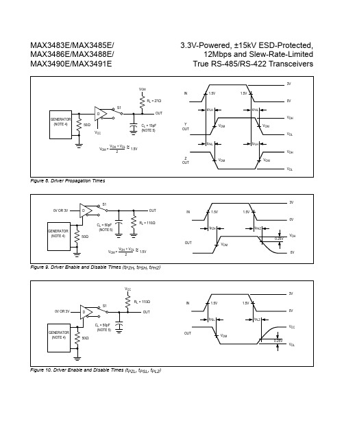
Figure 8. Driver Propagation TimesFigure 9. Driver Enable and Disable Times (t PZH , t PSH , t PHZ )Figure 10. Driver Enable and Disable Times (t PZL , t PSL , t PLZ )MAX3483E/MAX3485E/MAX3486E/MAX3488E/MAX3490E/MAX3491E3.3V-Powered, ±15kV ESD-Protected, 12Mbps and Slew-Rate-Limited True RS-485/RS-422 TransceiversDriver Output ProtectionExcessive output current and power dissipation caused by faults or by bus contention are prevented by two mechanisms. A foldback current limit on the output stage provides immediate protection against short circuits over the whole common-mode voltage range (see Typical Operating Characteristics ). In addition, a thermal shut-down circuit forces the driver outputs into a high-imped-ance state if the die temperature rises excessively.Propagation DelayFigures 15–18 show the typical propagation delays. Skew time is simply the difference between the low-to-high and high-to-low propagation delay. Small driver/receiver skew times help maintain a symmetrical mark-space ratio (50% duty cycle).The receiver skew time, |tPRLH - t PRHL |, is under 10ns 20ns for the MAX3483E/MAX3488E). The driver skew times are 8ns for the MAX3485E/MAX3490E/MAX3491E, 12ns for the MAX3486E, and typically under 50ns for the MAX3483E/MAX3488E.Line Length vs. Data RateThe RS-485/RS-422 standard covers line lengths up to 4000 feet. For line lengths greater than 4000 feet, see Figure 21 for an example of a line repeater.Figures 19 and 20 show the system differential voltage for parts driving 4000 feet of 26AWG twisted-pair wire at 125kHz into 120Ω loads.For faster data rate transmission, please consult the factory.±15kV ESD Protection As with all Maxim devices, ESD-protection structures are incorporated on all pins to protect against electrostatic discharges encountered during handling and assembly. The driver outputs and receiver inputs of the MAX3483E family of devices have extra protection against static electricity. Maxim’s engineers have developed state-of-the-art structures to protect these pins against ESD of ±15kV without damage. The ESD structures withstand high ESD in all states: normal operation, shutdown, and powered down. After an ESD event, Maxim’s E versions keep working without latchup or damage.ESD protection can be tested in various ways; the trans-mitter outputs and receiver inputs of this product family are characterized for protection to the following limits:1)±15kV using the Human Body Model 2)±8kV using the Contact-Discharge method specified in IEC 1000-4-23)±15kV using IEC 1000-4-2’s Air-Gap method.ESD Test Conditions ESD performance depends on a variety of conditions. Contact Maxim for a reliability report that documents test setup, test methodology, and test results.Human Body Model Figure 22a shows the Human Body Model and Figure 22b shows the current waveform it generates when dis-charged into a low impedance. This model consists of a 100pF capacitor charged to the ESD voltage of interest, which is then discharged into the test device through a 1.5kΩ resistor.IEC 1000-4-2The IEC 1000-4-2 standard covers ESD testing and performance of finished equipment; it does not specifi-cally refer to integrated circuits. The MAX3483E family of devices helps you design equipment that meets Level 4 (the highest level) of IEC 1000-4-2, without the need for additional ESD-protection components.The major difference between tests done using the Human Body Model and IEC 1000-4-2 is higher peak cur-rent in IEC 1000-4-2, because series resistance is lower in the IEC 1000-4-2 model. Hence, the ESD withstand voltage measured to IEC 1000-4-2 is generally lower than that measured using the Human Body Model. Figure 23a shows the IEC 1000-4-2 model, and Figure 23b shows the current waveform for the ±8kV IEC 1000-4-2, Level 4ESD contact-discharge test. test.Figure 21. Line Repeater for MAX3488E/MAX3490E/MAX3491EMAX3483E/MAX3485E/MAX3486E/MAX3488E/MAX3490E/MAX3491E3.3V-Powered, ±15kV ESD-Protected, 12Mbps and Slew-Rate-Limited True RS-485/RS-422 Transceivers。
MAX333AEWP中文资料

________________________________________________________________ Maxim Integrated Products
1
For free samples & the latest literature: , or phone 1-800-998-8800. For small orders, phone 1-800-835-8769.
元器件交易网
Precision, Quad, SPDT, CMOS Analog Switch MAX333A
ABSOLUTE MAXIMUM RATINGS
V+ to V- ..................................................................................44V VIN, VCOM, VNO, VNC ......................................................V- to V+ (VNO - VNC) ............................................................................32V V+ to Ground..........................................................................30V V- to Ground..........................................................................-30V Current, Any Terminal Except VCOM, VNO, or VNC .............30mA Continuous Current, VCOM, VNO, or VNC ............................20mA Peak Current, VCOM, VNO, or VNC (Pulsed at 1ms, 10% duty cycle max) ............................70mA ESD ....................................................................................2000V Note 1: Device mounted with all leads soldered to PC board. Continuous Power Dissipation (TA = +70°C) (Note 1) Plastic DIP (derate above +70°C by 11.11mW/°C) .....889mW SO (derate above +70°C by 10.00mW/°C) ..................800mW CERDIP (derate above +70°C by 11.11mW/°C) ..........889mW TSSOP (derate above +70°C by 7mW/°C) ..................559mW Operating Temperature Ranges: MAX333AC_ _ .....................................................0°C to +70°C MAX333AE_ _ ..................................................-40°C to +85°C MAX333AMJP ................................................-55°C to +125°C Storage Temperature Range .............................-65°C to +150°C Lead Temperature (soldering, 10sec) .............................+300°C
MAX4080TASA+中文资料
元器件交易网
MAX4080/MAX4081
19-2562; Rev 0; 10/02
EVAALVUAAILTAIOBNLEKIT
76V, High-Side, Current-Sense Amplifiers with Voltage Output
General Description
General System/Board-Level Current Sensing
Precision High-Voltage Current Sources
Features
♦ Wide 4.5V to 76V Input Common-Mode Range ♦ Bidirectional or Unidirectional ISENSE ♦ Low-Cost, Compact, Current-Sense Solution ♦ Three Gain Versions Available
(MAX4081 Only)....-0.3V to the lesser of +18V or (VCC + 0.3V) Output Short Circuit to GND.......................................Continuous Differential Input Voltage (VRS+ - VRS-) ...............................±80V Current into Any Pin..........................................................±20mA
MAX412CSA+,MAX412ESA+,MAX410ESA+,MAX412CPA+,MAX412EPA+,MAX414CSD+,MAX410BCSA, 规格书,Datasheet 资料

Applications
Low-Noise Frequency Synthesizers Infrared Detectors High-Quality Audio Amplifiers Ultra Low-Noise Instrumentation Amplifiers Bridge Signal Conditioning
ELECTRICAL CHARACTERISTICS
(V+ = 5V, V- = -5V, TA = +25°C, unless otherwise noted.)
PARAMETER Input Offset Voltage Input Bias Current Input Offset Current Differential Input Resistance Common-Mode Input Resistance Input Capacitance SYMBOL VOS IB IOS RIN(Diff) RIN(CM) CIN MAX410, MAX412, MAX414 Input Noise-Voltage Density en MAX410B, MAX412B, MAX414B fO = 10Hz fO = 1000Hz ±3.5 VCM = ±3.5V VS = ±2.4V to ±5.25V RL = 2kΩ, VO = ±3.6V RL = 600Ω, VO = ±3.5V RL = 2kΩ 115 96 115 110 +3.6 -3.7 10Hz 1000Hz (Note 2) 1000Hz (Note 2) CONDITIONS MAX410, MAX410B, MAX412, MAX412B MAX414, MAX414B MIN TYP ±120 ±150 ±80 ±40 20 40 4 7 1.5 2.4 2.6 1.2 +3.7/ -3.8 130 103 122 120 +3.7/ -3.8 35 10kΩ || 20pF load 10kΩ || 20pF load To 0.1% fO = 1kHz 4.5 28 1.3 135 2.4 4.0 pA√Hz V dB dB dB V mA V/µs MHz µs dB nV√Hz MAX ±250 ±320 ±150 ±80 UNITS µV nA nA kΩ MΩ pF
最低静态电流的超小尺寸降压转换器

新品发布NEW PRODUCTS今日电子 · 2018年5月 · 外带来新的层面,例如,混光。
整合式M O S F E T额定60V,使A L8862成为可行的解决方案,可用于更高功率的输出应用。
利用Diodes公司的专有技术,M O S F E T也具备仅0.4Ω的超低R D S(O N),能在缩减外部零件需求的同时展现出高效率。
亦针对短路或开路可能造成的故障情形提供完整保护,同时包含了过热保护。
Diodes Incorporated线性LED控制器A L5814、A L5817、A L5815及AL5816线性LED控制器,为LED灯条提供可调光和可调节的驱动电流,效率高达80%以上。
A L58x x系列提供物料列表(B O M)成本低廉的解决方案,适用于商业和工业领域的各项产品应用,包括广告牌、仪器照明、家电内部照明、建筑细部照明,以及一般智能照明设备。
这些装置的输入范围为4.5~60V,无须电感,可保持良好的E M I效能,使系统整合更简单。
此外,相较于其他设计,外部功率晶体管可使内部功耗降至最低。
A L58x x系列可提供高达15m A 的电流给外部MOSFET或双极晶体管,以驱动LED灯条。
LED驱动电流由一个外部电阻配置,具有4%的参考电压准确度,以及出色的温度稳定性。
不仅如此,AL5815与AL5816装置支持PWM调光功能,A L5814与A L5817装置则同时支持模拟和PWM调光功能。
保护功能包括过温保护及输入欠压锁定。
A L5814及A L5817装置也利用VFAULT脚位提供「LED 开回路」保护功能,以及L E D 热回流保护。
A L58x x系列线性控制器提供良好的E M I效能,而广泛的工作温度范围(-40~+105℃)使其适用于恶劣环境。
Diodes Incorporated超小电源模块MAXM17532和MAXM15462超小尺寸(2.6mm×3.0mm×1.5mm)、集成式DC-DC电源模块是Maxim喜马拉雅电源方案专有组合的一部分,适用于工业、医疗健康、通信和消费市场。
MAX1241中文资料datasheet

MAX1240 / MAX1241 采用 8 引脚封装的低 功耗、12 位模数转换器转换器(ADC)。 MAX1240 采 用 + 2.7V 至 + 3.6V 的 电 源 供 电,MAX1241 采用单电源供电范围是+ 2.7V 至+ 5.25V。这两款设备都具有 7.5μs 的功 能 逐次逼近 ADC,快速跟踪/保持(1.5μs), 片上时钟和高速 3 线串行接口。 在 73ksps 的 最 大 采 样 速 度 下 , 功 耗 仅 为 37mW(VDD = 3V)。2μA 关断模式以较 慢的吞吐率来降低功耗。 MAX1240 具 有 内 部 2.5V 参 考 电 压 , 而 MAX1241 需要外部参考电 压。MAX1241 接受从 0V 到VREF 和参考信号输入范围包括 正电源轨。外部的时钟从 3 线接口访问数据, 它直接连接到标准微控制器的 I/O 港口。该 接口与 SPI™,QSPI™和 MICROWIRE™兼容。 该接卓越的交流特性和极低的功耗,易于使 用和小封装尺寸,使这些转换器成为远程传 感器和数据采集应用的理想之选,或者是要 求降低功耗和对空间有要求的电路的最好 选择。MAX1240/MAX1241 采用 8 引脚 PDIP 和 SO 封装。
兑换率
转换时间 跟踪/保持采集时 间 转换时间 吞吐率 光圈抖动
tCONV
t ACQ
t APR
fSCLK=2.1MHz 图8
5.5
7.5
us
1.5
us
73
ksps
30
ns
<50
ps
模拟输入
输入电压范围 输入电容
0
VREF V
16
pF
电源要求
MAX202CSE中文资料
General DescriptionThe MAX200–MAX211/MAX213 transceivers are designed for RS-232 and V.28 communication inter-faces where ±12V supplies are not available. On-board charge pumps convert the +5V input to the ±10V need-ed for RS-232 output levels. The MAX201 and MAX209operate from +5V and +12V, and contain a +12V to -12V charge-pump voltage converter.The MAX200–MAX211/MAX213 drivers and receivers meet all EIA/TIA-232E and CCITT V.28 specifications at a data rate of 20kbps. The drivers maintain the ±5V EIA/TIA-232E output signal levels at data rates in excess of 120kbps when loaded in accordance with the EIA/TIA-232E specification.The 5µW shutdown mode of the MAX200, MAX205,MAX206, and MAX211 conserves energy in battery-powered systems. The MAX213 has an active-low shut-down and an active-high receiver enable control. Two receivers of the MAX213 are active, allowing ring indica-tor (RI) to be monitored easily using only 75µW power.The MAX211 and MAX213 are available in a 28-pin wide small-outline (SO) package and a 28-pin shrink small-outline (SSOP) package, which occupies only 40% of the area of the SO. The MAX207 is now avail-able in a 24-pin SO package and a 24-pin SSOP. The MAX203 and MAX205 use no external components,and are recommended for applications with limited circuit board space.ApplicationsComputersLaptops, Palmtops, Notebooks Battery-Powered Equipment Hand-Held Equipment Next-Generation Device Features ♦For Low-Cost Applications:MAX221E: ±15kV ESD-Protected, +5V, 1µA, Single RS-232 Transceiver with AutoShutdown™♦For Low-Voltage and Space-Constrained Applications:MAX3222E/MAX3232E/MAX3237E/MAX3241E/MAX3246E: ±15kV ESD-Protected, Down to 10nA,+3.0V to +5.5V, Up to 1Mbps, True RS-232Transceivers (MAX3246E Available in UCSP™Package)♦For Space-Constrained Applications:MAX3228E/MAX3229E: ±15kV ESD-Protected,+2.5V to +5.5V, RS-232 Transceivers in UCSP ♦For Low-Voltage or Data Cable Applications:MAX3380E/MAX3381E: +2.35V TO +5.5V, 1µA,2Tx/2Rx RS-232 Transceivers with ±15kV ESD-Protected I/O and Logic Pins ♦For Low-Power Applications:MAX3224E–MAX3227E/MAX3244E/MAX3245E:±15kV ESD-Protected, 1µA, 1Mbps, +3.0V to+5.5V, RS-232 Transceivers with AutoShutdown Plus™MAX200–MAX211/MAX213+5V , RS-232 Transceivers with 0.1µF External Capacitors ________________________________________________________________Maxim Integrated Products 119-0065; Rev 6; 10/03For pricing, delivery, and ordering information,please contact Maxim/Dallas Direct!at 1-888-629-4642, or visit Maxim’s website at .Ordering Information appears at end of data sheetAutoShutdown, AutoShutdown Plus, and UCSP are trademarks of Maxim Integrated Products, Inc.MAX200–MAX211/MAX213+5V , RS-232 Transceiverswith 0.1µF External Capacitors______________________________________________________________________________________19Ordering Information*Contact factory for dice specifications.M A X 200–M A X 211/M A X 213+5V , RS-232 Transceiverswith 0.1µF External Capacitors Maxim cannot assume responsibility for use of any circuitry other than circuitry entirely embodied in a Maxim product. No circuit patent licenses are implied. Maxim reserves the right to change the circuitry and specifications without notice at any time.20____________________Maxim Integrated Products, 120 San Gabriel Drive, Sunnyvale, CA 94086 408-737-7600©2003 Maxim Integrated ProductsPrinted USAis a registered trademark of Maxim Integrated Products.Package Information(The package drawing(s) in this data sheet may not reflect the most current specifications. For the latest package outline information,go to /packages .)。
MAX3051ESA中文资料
ELECTRICAL CHARACTERISTICS
(VCC = +3.3V ±5%, RL = 60Ω, CL = 100pF, TA = TMIN to TMAX, unless otherwise noted. Typical values are at VCC = +3.3V and TA = +25°C.) (Note 1)
CONDITIONS
Recessive
Standby
VSHDN = VCC, TXD = VCC or floating
MIN TYP MAX UNITS
35
70
mA
2
5
8
15
µA
1
µA
+160
°C
25
°C
VIH
VIL CIN RINTXD
2
VCC +
V
0.3V
MAX490EESA+资料
Supply Control
Voltage (VCC) Input Voltage
.(.–R—..E.–..,..D..E..)........................................-.0....5..V...t.o...(.V..C...C...+...0...152VV)
♦ For Low-Voltage Applications: MAX3483E/MAX3485E/MAX3486E/MAX3488E/ MAX3490E/MAX3491E: +3.3V Powered, ±15kV ESD-Protected, 12Mbps, Slew-Rate-Limited, True RS-485/RS-422 Transceivers
General Description
The MAX481E, MAX483E, MAX485E, MAX487E– MAX491E, and MAX1487E are low-power transceivers for RS-485 and RS-422 communications in harsh environments. Each driver output and receiver input is protected against ±15kV electro-static discharge (ESD) shocks, without latchup. These parts contain one driver and one receiver. The MAX483E, MAX487E, MAX488E, and MAX489E feature reduced slew-rate drivers that minimize EMI and reduce reflections caused by improperly terminated cables, thus allowing error-free data transmission up to 250kbps. The driver slew rates of the MAX481E, MAX485E, MAX490E, MAX491E, and MAX1487E are not limited, allowing them to transmit up to 2.5Mbps.
MAX202EEPE中文资料

________________________________________________________________Maxim Integrated Products 1General DescriptionThe MAX202E–MAX213E, MAX232E/MAX241E line drivers/receivers are designed for RS-232 and V.28communications in harsh environments. Each transmitter output and receiver input is protected against ±15kV electrostatic discharge (ESD) shocks, without latchup.The various combinations of features are outlined in the Selector Guide.The drivers and receivers for all ten devices meet all EIA/TIA-232E and CCITT V.28specifications at data rates up to 120kbps, when loaded in accordance with the EIA/TIA-232E specification.The MAX211E/MAX213E/MAX241E are available in 28-pin SO packages, as well as a 28-pin SSOP that uses 60% less board space. The MAX202E/MAX232E come in 16-pin TSSOP, narrow SO, wide SO, and DIP packages. The MAX203E comes in a 20-pin DIP/SO package, and needs no external charge-pump capacitors. The MAX205E comes in a 24-pin wide DIP package, and also eliminates external charge-pump capacitors. The MAX206E/MAX207E/MAX208E come in 24-pin SO, SSOP, and narrow DIP packages. The MAX232E/MAX241E operate with four 1µF capacitors,while the MAX202E/MAX206E/MAX207E/MAX208E/MAX211E/MAX213E operate with four 0.1µF capacitors,further reducing cost and board space.________________________ApplicationsNotebook, Subnotebook, and Palmtop Computers Battery-Powered Equipment Hand-Held EquipmentNext-Generation Device Featureso For Low-Voltage ApplicationsMAX3222E/MAX3232E/MAX3237E/MAX3241E/MAX3246E: ±15kV ESD-Protected Down to10nA, +3.0V to +5.5V, Up to 1Mbps, True RS-232Transceivers (MAX3246E Available in a UCSP™Package)o For Low-Power ApplicationsMAX3221/MAX3223/MAX3243: 1µA SupplyCurrent, True +3V to +5.5V RS-232 Transceivers with Auto-Shutdown™o For Space-Constrained ApplicationsMAX3233E/MAX3235E: ±15kV ESD-Protected,1µA, 250kbps, +3.0V/+5.5V, Dual RS-232Transceivers with Internal Capacitorso For Low-Voltage or Data Cable ApplicationsMAX3380E/MAX3381E: +2.35V to +5.5V, 1µA,2Tx/2Rx RS-232 Transceivers with ±15kV ESD-Protected I/O and Logic PinsMAX202E–MAX213E, MAX232E/MAX241E±15kV ESD-Protected, +5V RS-232 TransceiversSelector Guide19-0175; Rev 6; 3/05Pin Configurations and Typical Operating Circuits appear at end of data sheet.YesPARTNO. OF RS-232DRIVERSNO. OF RS-232RECEIVERSRECEIVERS ACTIVE IN SHUTDOWNNO. OF EXTERNAL CAPACITORS(µF)LOW-POWER SHUTDOWNTTL TRI-STATE MAX202E 220 4 (0.1)No No MAX203E 220None No No MAX205E 550None Yes Yes MAX206E 430 4 (0.1)Yes Yes MAX207E 530 4 (0.1)No No MAX208E 440 4 (0.1)No No MAX211E 450 4 (0.1)Yes Yes MAX213E 452 4 (0.1)Yes Yes MAX232E 220 4 (1)No No MAX241E454 (1)YesFor pricing, delivery, and ordering information,please contact Maxim/Dallas Direct!at 1-888-629-4642, or visit Maxim’s website at .AutoShutdown and UCSP are trademarks of Maxim Integrated Products, Inc.Ordering InformationOrdering Information continued at end of data sheet.2_______________________________________________________________________________________M A X 202E –M A X 213E , M A X 232E /M A X 241EABSOLUTE MAXIMUM RATINGSV CC ..........................................................................-0.3V to +6V V+................................................................(V CC - 0.3V) to +14V V-............................................................................-14V to +0.3V Input VoltagesT_IN............................................................-0.3V to (V+ + 0.3V)R_IN...................................................................................±30V Output VoltagesT_OUT.................................................(V- - 0.3V) to (V+ + 0.3V)R_OUT......................................................-0.3V to (V CC + 0.3V)Short-Circuit Duration, T_OUT....................................Continuous Continuous Power Dissipation (T A = +70°C)16-Pin Plastic DIP (derate 10.53mW/°C above +70°C)....842mW 16-Pin Narrow SO (derate 8.70mW/°C above +70°C).....696mW 16-Pin Wide SO (derate 9.52mW/°C above +70°C)......762mW 16-Pin TSSOP (derate 9.4mW/°C above +70°C)...........755mW20-Pin Plastic DIP (derate 11.11mW/°C above +70°C)...889mW 20-Pin SO (derate 10.00mW/°C above +70°C).............800mW 24-Pin Narrow Plastic DIP(derate 13.33mW/°C above +70°C) ...............................1.07W 24-Pin Wide Plastic DIP(derate 14.29mW/°C above +70°C)................................1.14W 24-Pin SO (derate 11.76mW/°C above +70°C).............941mW 24-Pin SSOP (derate 8.00mW/°C above +70°C)..........640mW 28-Pin SO (derate 12.50mW/°C above +70°C)....................1W 28-Pin SSOP (derate 9.52mW/°C above +70°C)..........762mW Operating Temperature RangesMAX2_ _EC_ _.....................................................0°C to +70°C MAX2_ _EE_ _...................................................-40°C to +85°C Storage Temperature Range.............................-65°C to +165°C Lead Temperature (soldering, 10s).................................+300°CELECTRICAL CHARACTERISTICS(V CC = +5V ±10% for MAX202E/206E/208E/211E/213E/232E/241E; V CC = +5V ±5% for MAX203E/205E/207E; C1–C4 = 0.1µF for MAX202E/206E/207E/208E/211E/213E; C1–C4 = 1µF for MAX232E/241E; T A = T MIN to T MAX ; unless otherwise noted. Typical values are at T A = +25°C.)Stresses beyond those listed under “Absolute Maximum Ratings” may cause permanent damage to the device. These are stress ratings only, and functional operation of the device at these or any other conditions beyond those indicated in the operational sections of the specifications is not implied. Exposure to absolute maximum rating conditions for extended periods may affect device reliability.ELECTRICAL CHARACTERISTICS (continued)MAX202E–MAX213E, MAX232E/MAX241E (V CC= +5V ±10% for MAX202E/206E/208E/211E/213E/232E/241E; V CC= +5V ±5% for MAX203E/205E/207E; C1–C4 = 0.1µF forMAX202E/206E/207E/208E/211E/213E; C1–C4 = 1µF for MAX232E/241E; T A= T MIN to T MAX; unless otherwise noted. Typical valuesare at T A= +25°C.)Note 1:MAX211EE_ _ tested with V CC= +5V ±5%._______________________________________________________________________________________34______________________________________________________________________________________M A X 202E –M A X 213E , M A X 232E /M A X 241E__________________________________________Typical Operating Characteristics(Typical Operating Circuits, V CC = +5V, T A = +25°C, unless otherwise noted.)5.00MAX211E/MAX213ETRANSMITTER OUTPUT VOLTAGEvs. LOAD CAPACITANCELOAD CAPACITANCE (pF)V O H , -V O L (V )5.56.06.57.07.58.0100020003000400050000MAX211E/MAX213E/MAX241E TRANSMITTER SLEW RATE vs. LOAD CAPACITANCELOAD CAPACITANCE (pF)S L E W R A T E ( V /µs )5101520253010002000300040005000_______________________________________________________________________________________5MAX202E–MAX213E, MAX232E/MAX241E____________________________Typical Operating Characteristics (continued)(Typical Operating Circuits, V CC = +5V, T A = +25°C, unless otherwise noted.)2MAX202E/MAX203E/MAX232E TRANSMITTER SLEW RATE vs. LOAD CAPACITANCELOAD CAPACITANCE (pF)S L E W R A T E ( V /µs )468101214100020003000400050005.07.5-7.53000MAX205E–MAX208ETRANSMITTER OUTPUT VOLTAGEvs. LOAD CAPACITANCE-5.02.5LOAD CAPACITANCE (pF)O U T P U T V O L T A G E (V )10002000400050000-2.54550203000MAX205E–MAX208E SUPPLY CURRENT vs. LOAD CAPACITANCE2540LOAD CAPACITANCE (pF)S U P P L Y C U R R E N T (m A )100020004000500035302.55.0-10.0180MAX205E –MAX208EOUTPUT VOLTAGE vs. DATA RATE-7.50DATA RATE (kbps)O U T P U T V O L T A G E (V )601202401503090210-2.5-5.010.07.56_______________________________________________________________________________________M A X 202E –M A X 213E , M A X 232E /M A X 241EMAX203EMAX205E_____________________________________________________________Pin DescriptionsMAX202E/MAX232E_______________________________________________________________________________________7MAX202E–MAX213E, MAX232E/MAX241EMAX208E________________________________________________Pin Descriptions (continued)MAX206EMAX207E8_______________________________________________________________________________________M A X 202E –M A X 213E , M A X 232E /M A X 241EMAX211E/MAX213E/MAX241E)(MAX205E/MAX206E/MAX211E/MAX213E/MAX241E)________________________________________________Pin Descriptions (continued)MAX211E/MAX213E/MAX241EFigure 3. Transition Slew-Rate Circuit_______________Detailed Description The MAX202E–MAX213E, MAX232E/MAX241E consist of three sections: charge-pump voltage converters, drivers (transmitters), and receivers. These E versions provide extra protection against ESD. They survive ±15kV discharges to the RS-232 inputs and outputs, tested using the Human Body Model. When tested according to IEC1000-4-2, they survive ±8kV contact-discharges and ±15kV air-gap discharges. The rugged E versions are intended for use in harsh environments or applications where the RS-232 connection is frequently changed (such as notebook computers). The standard (non-“E”) MAX202, MAX203, MAX205–MAX208, MAX211, MAX213, MAX232, and MAX241 are recommended for applications where cost is critical.+5V to ±10V Dual Charge-PumpVoltage Converter The +5V to ±10V conversion is performed by dual charge-pump voltage converters (Figure 4). The first charge-pump converter uses capacitor C1 to double the +5V into +10V, storing the +10V on the output filter capacitor, C3. The second uses C2 to invert the +10V into -10V, storing the -10V on the V- output filter capacitor, C4.In shutdown mode, V+ is internally connected to V CC by a 1kΩpull-down resistor, and V- is internally connected to ground by a 1kΩpull up resistor.RS-232 Drivers With V CC= 5V, the typical driver output voltage swing is ±8V when loaded with a nominal 5kΩRS-232 receiver. The output swing is guaranteed to meet EIA/TIA-232E and V.28 specifications that call for ±5V minimum output levels under worst-case conditions. These include a 3kΩload, minimum V CC, and maximum operating temperature. The open-circuit output voltage swings from (V+ - 0.6V) to V-.Input thresholds are CMOS/TTL compatible. The unused drivers’ inputs on the MAX205E–MAX208E, MAX211E, MAX213E, and MAX241E can be left unconnected because 400kΩpull up resistors to V CC are included on-chip. Since all drivers invert, the pull up resistors force the unused drivers’ outputs low. The MAX202E, MAX203E, and MAX232E do not have pull up resistors on the transmitter inputs._______________________________________________________________________________________9MAX202E–MAX213E, MAX232E/MAX241E10______________________________________________________________________________________M A X 202E –M A X 213E , M A X 232E /M A X 241E±15kV ESD-Protected, +5V RS-232 Transceivers When in low-power shutdown mode, the MAX205E/MAX206E/MAX211E/MAX213E/MAX241E driver outputs are turned off and draw only leakage currents—even if they are back-driven with voltages between 0V and 12V. Below -0.5V in shutdown, the transmitter output is diode-clamped to ground with a 1k Ωseries impedance.RS-232 ReceiversThe receivers convert the RS-232 signals to CMOS-logic output levels. The guaranteed 0.8V and 2.4V receiver input thresholds are significantly tighter than the ±3V thresholds required by the EIA/TIA-232E specification.This allows the receiver inputs to respond to TTL/CMOS-logic levels, as well as RS-232 levels.The guaranteed 0.8V input low threshold ensures that receivers shorted to ground have a logic 1 output. The 5k Ωinput resistance to ground ensures that a receiver with its input left open will also have a logic 1 output. Receiver inputs have approximately 0.5V hysteresis.This provides clean output transitions, even with slow rise/fall-time signals with moderate amounts of noise and ringing.In shutdown, the MAX213E’s R4 and R5 receivers have no hysteresis.Shutdown and Enable Control (MAX205E/MAX206E/MAX211E/MAX213E/MAX241E)In shutdown mode, the charge pumps are turned off,V+ is pulled down to V CC , V- is pulled to ground, and the transmitter outputs are disabled. This reduces supply current typically to 1µA (15µA for the MAX213E).The time required to exit shutdown is under 1ms, as shown in Figure 5.ReceiversAll MAX213E receivers, except R4 and R5, are put into a high-impedance state in shutdown mode (see Tables 1a and 1b). The MAX213E’s R4 and R5 receivers still function in shutdown mode. These two awake-in-shutdown receivers can monitor external activity while maintaining minimal power consumption.The enable control is used to put the receiver outputs into a high-impedance state, to allow wire-OR connection of two EIA/TIA-232E ports (or ports of different types) at the UART. It has no effect on the RS-232 drivers or the charge pumps.N ote: The enabl e control pin is active l ow for the MAX211E/MAX241E (EN ), but is active high for the MAX213E (EN). The shutdown control pin is active high for the MAX205E/MAX206E/MAX211E/MAX241E (SHDN), but is active low for the MAX213E (SHDN ).Figure 4. Charge-Pump DiagramMAX202E–MAX213E, MAX232E/MAX241EV+V-200µs/div3V 0V 10V 5V 0V -5V -10VSHDNMAX211EFigure 5. MAX211E V+ and V- when Exiting Shutdown (0.1µF capacitors)X = Don't care.*Active = active with reduced performanceSHDN E N OPERATION STATUS Tx Rx 00Normal Operation All Active All Active 01Normal Operation All Active All High-Z 1XShutdownAll High-ZAll High-ZTable 1a. MAX205E/MAX206E/MAX211E/MAX241E Control Pin ConfigurationsTable 1b. MAX213E Control Pin ConfigurationsThe MAX213E’s receiver propagation delay is typically 0.5µs in normal operation. In shutdown mode,propagation delay increases to 4µs for both rising and falling transitions. The MAX213E’s receiver inputs have approximately 0.5V hysteresis, except in shutdown,when receivers R4 and R5 have no hysteresis.When entering shutdown with receivers active, R4 and R5 are not valid until 80µs after SHDN is driven low.When coming out of shutdown, all receiver outputs are invalid until the charge pumps reach nominal voltage levels (less than 2ms when using 0.1µF capacitors).±15kV ESD ProtectionAs with all Maxim devices, ESD-protection structures are incorporated on all pins to protect against electrostatic discharges encountered during handling and assembly. The driver outputs and receiver inputs have extra protection against static electricity. Maxim’s engineers developed state-of-the-art structures to protect these pins against ESD of ±15kV without damage. The ESD structures withstand high ESD in all states: normal operation, shutdown, and powered down. After an ESD event, Maxim’s E versions keep working without latchup, whereas competing RS-232products can latch and must be powered down to remove latchup.ESD protection can be tested in various ways; the transmitter outputs and receiver inputs of this product family are characterized for protection to the following limits:1)±15kV using the Human Body Model2)±8kV using the contact-discharge method specifiedin IEC1000-4-23)±15kV using IEC1000-4-2’s air-gap method.ESD Test ConditionsESD performance depends on a variety of conditions.Contact Maxim for a reliability report that documents test set-up, test methodology, and test results.Human Body ModelFigure 6a shows the Human Body Model, and Figure 6b shows the current waveform it generates when discharged into a low impedance. This model consists of a 100pF capacitor charged to the ESD voltage of interest, which is then discharged into the test device through a 1.5k Ωresistor.S H D N ENOPERATION STATUS Tx 1–400Shutdown All High-Z 01Shutdown All High-Z 10Normal Operation 11Normal OperationAll ActiveAll Active Active1–34, 5High-Z ActiveHigh-Z High-Z High-Z Active*High-Z RxM A X 202E –M A X 213E , M A X 232E /M A X 241EIEC1000-4-2The IEC1000-4-2 standard covers ESD testing and performance of finished equipment; it does not specifically refer to integrated circuits. The MAX202E/MAX203E–MAX213E, MAX232E/MAX241E help you design equipment that meets level 4 (the highest level) of IEC1000-4-2, without the need for additional ESD-protection components.The major difference between tests done using the Human Body Model and IEC1000-4-2 is higher peak current in IEC1000-4-2, because series resistance is lower in the IEC1000-4-2 model. Hence, the ESD withstand voltage measured to IEC1000-4-2 is generally lower than that measured using the Human Body Model. Figure 7b shows the current waveform for the 8kV IEC1000-4-2 level-four ESD contact-discharge test.The air-gap test involves approaching the device with a charged probe. The contact-discharge method connects the probe to the device before the probe is energized.Machine ModelThe Machine Model for ESD tests all pins using a 200pF storage capacitor and zero discharge resistance. Its objective is to emulate the stress caused by contact that occurs with handling and assembly during manufacturing. Of course, all pins require this protection during manufacturing, not just RS-232 inputs and outputs. Therefore,after PC board assembly,theMachine Model is less relevant to I/O ports.Figure 7a. IEC1000-4-2 ESD Test ModelFigure 7b. IEC1000-4-2 ESD Generator Current WaveformFigure 6a. Human Body ESD Test ModelFigure 6b. Human Body Model Current Waveform__________Applications InformationCapacitor Selection The capacitor type used for C1–C4 is not critical for proper operation. The MAX202E, MAX206–MAX208E, MAX211E, and MAX213E require 0.1µF capacitors, and the MAX232E and MAX241E require 1µF capacitors, although in all cases capacitors up to 10µF can be used without harm. Ceramic, aluminum-electrolytic, or tantalum capacitors are suggested for the 1µF capacitors, and ceramic dielectrics are suggested for the 0.1µF capacitors. When using the minimum recommended capacitor values, make sure the capacitance value does not degrade excessively as the operating temperature varies. If in doubt, use capacitors with a larger (e.g., 2x) nominal value. The capacitors’ effective series resistance (ESR), which usually rises at low temperatures, influences the amount of ripple on V+ and V-.Use larger capacitors (up to 10µF) to reduce the output impedance at V+ and V-. This can be useful when “stealing” power from V+ or from V-. The MAX203E and MAX205E have internal charge-pump capacitors. Bypass V CC to ground with at least 0.1µF. In applications sensitive to power-supply noise generated by the charge pumps, decouple V CC to ground with a capacitor the same size as (or larger than) the charge-pump capacitors (C1–C4).V+ and V- as Power Supplies A small amount of power can be drawn from V+ and V-, although this will reduce both driver output swing and noise margins. Increasing the value of the charge-pump capacitors (up to 10µF) helps maintain performance when power is drawn from V+ or V-.Driving Multiple Receivers Each transmitter is designed to drive a single receiver. Transmitters can be paralleled to drive multiple receivers.Driver Outputs when Exiting Shutdown The driver outputs display no ringing or undesirable transients as they come out of shutdown.High Data Rates These transceivers maintain the RS-232 ±5.0V minimum driver output voltages at data rates of over 120kbps. For data rates above 120kbps, refer to the Transmitter Output Voltage vs. Load Capacitance graphs in the Typical Operating Characteristics. Communication at these high rates is easier if the capacitive loads on the transmitters are small; i.e., short cables are best.Table 2. Summary of EIA/TIA-232E, V.28 SpecificationsMAX202E–MAX213E, MAX232E/MAX241EM A X 202E –M A X 213E , M A X 232E /M A X 241E____________Pin Configurations and Typical Operating Circuits (continued)Table 3. DB9 Cable ConnectionsCommonly Used for EIA/TIAE-232E and V.24 Asynchronous Interfaces____________Pin Configurations and Typical Operating Circuits (continued)MAX202E–MAX213E, MAX232E/MAX241EM A X 202E –M A X 213E , M A X 232E /M A X 241E____________Pin Configurations and Typical Operating Circuits (continued)MAX202E–MAX213E, MAX232E/MAX241E____________Pin Configurations and Typical Operating Circuits (continued)M A X 202E –M A X 213E , M A X 232E /M A X 241E____________Pin Configurations and Typical Operating Circuits (continued)MAX202E–MAX213E, MAX232E/MAX241E____________Pin Configurations and Typical Operating Circuits (continued)M A X 202E –M A X 213E , M A X 232E /M A X 241E____________Pin Configurations and Typical Operating Circuits (continued)______________________________________________________________________________________21MAX202E–MAX213E, MAX232E/MAX241E Ordering Information (continued)*Dice are specified at T A= +25°C.M A X 202E –M A X 213E , M A X 232E /M A X 241E22________________________________________________________________________________________________________________________________________________Chip Topographies___________________Chip InformationC1-V+C1+V CC R2INT2OUT R2OUT0.117"(2.972mm)0.080"(2.032mm)V-C2+ C2-T2IN T1OUT R1INR1OUT T1INGNDR5INV-C2-C2+C1-V+C1+V CC T4OUTR3IN T3OUTT1OUT 0.174"(4.420mm)0.188"(4.775mm)T4IN R5OUT R4OUT T3IN R4IN EN (EN) SHDN (SHDN)R3OUT T2OUT GNDR1IN R1OUT T2IN R2OUTR2IN T1IN ( ) ARE FOR MAX213E ONLYTRANSISTOR COUNT: 123SUBSTRATE CONNECTED TO GNDTRANSISTOR COUNT: 542SUBSTRATE CONNECTED TO GNDMAX202E/MAX232EMAX211E/MAX213E/MAX241EMAX205E/MAX206E/MAX207E/MAX208E TRANSISTOR COUNT: 328SUBSTRATE CONNECTED TO GNDMAX202E–MAX213E, MAX232E/MAX241E Package InformationM A X 202E –M A X 213E , M A X 232E /M A X 241EPackage Information (continued)MAX202E–MAX213E, MAX232E/MAX241E±15kV ESD-Protected, +5V RS-232 TransceiversMaxim cannot assume responsibility for use of any circuitry other than circuitry entirely embodied in a Maxim product. No circuit patent licenses are implied. Maxim reserves the right to change the circuitry and specifications without notice at any time.Maxim Integrated Products, 120 San Gabriel Drive, Sunnyvale, CA 94086 408-737-7600 ____________________25©2005 Maxim Integrated ProductsPrinted USAis a registered trademark of Maxim Integrated Products, Inc.Package Information (continued)(The package drawing(s) in this data sheet may not reflect the most current specifications. For the latest package outline information go to /packages .)。
MAX5841中文资料
o Rail-to-Rail Output Buffer Amplifiers
o Three Software-Selectable Power-Down Output Impedances 100kΩ, 1kΩ, and High Impedance
ELECTRICAL CHARACTERISTICS
(VDD = +2.7V to +5.5V, GND = 0, VREF = VDD, RL = 5kΩ, CL = 200pF, TA = TMIN to TMAX, unless otherwise noted. Typical values are at VDD = +5V, TA = +25°C.) (Note 1)
元器件交易网
19-1777; Rev 0; 1/02
MAX5841
Quad, 10-Bit, Low-Power, 2-Wire, Serial Voltage-Output DAC
General Description
The MAX5841 is a quad, 10-bit voltage output, digitalto-analog converter (DAC) with an I2C™-compatible, 2-wire interface that operates at clock rates up to 400kHz. The device operates from a single 2.7V to 5.5V supply and draws only 230µA at VDD = 3.6V. A powerdown mode decreases current consumption to less than 1µA. The MAX5841 features three software-selectable power-down output impedances: 100kΩ, 1kΩ, and high impedance. Other features include internal precision Rail-to-Rail® output buffers and a power-on reset (POR) circuit that powers up the DAC in the 100kΩ power-down mode. The MAX5841 features a double-buffered I2C-compatible serial interface that allows multiple devices to share a single bus. All logic inputs are CMOS-logic compatible and buffered with Schmitt triggers, allowing direct interfacing to optocoupled and transformer-isolated interfaces. The MAX5841 minimizes digital noise feedthrough by disconnecting the clock (SCL) signal from the rest of the device when an address mismatch is detected.
- 1、下载文档前请自行甄别文档内容的完整性,平台不提供额外的编辑、内容补充、找答案等附加服务。
- 2、"仅部分预览"的文档,不可在线预览部分如存在完整性等问题,可反馈申请退款(可完整预览的文档不适用该条件!)。
- 3、如文档侵犯您的权益,请联系客服反馈,我们会尽快为您处理(人工客服工作时间:9:00-18:30)。
General DescriptionThe MAX4051/MAX4052/MAX4053 and MAX4051A/MAX4052A/MAX4053A are low-voltage, CMOS analog ICs configured as an 8-channel multiplexer (MAX4051/A),two 4-channel multiplexers (MAX4052/A), and three sin-gle-pole/double-throw (SPDT) switches (MAX4053/A).The A-suffix parts are fully characterized for on-resistance match, on-resistance flatness, and low leakage.These CMOS devices can operate continuously with dual power supplies ranging from ±2.7V to ±8V or a single supply between +2.7V and +16V. Each switch can handle rail-to-rail analog signals. The off-leakage current is only 0.1nA at +25°C or 5nA at +85°C (MAX4051A/MAX4052A/MAX4053A).All digital inputs have 0.8V to 2.4V logic thresholds,ensuring TTL/CMOS-logic compatibility when using ±5V or a single +5V supply.________________________ApplicationsBattery-Operated Equipment Audio and Video Signal Routing Low-Voltage Data-Acquisition Systems Communications Circuits____________________________Features♦Pin Compatible with Industry-Standard74HC4051/74HC4052/74HC4053♦Guaranteed On-Resistance:100Ωwith ±5V Supplies♦Guaranteed Match Between Channels:6Ω(MAX4051A–MAX4053A)12Ω(MAX4051–MAX4053)♦Guaranteed Low Off-Leakage Currents:0.1nA at +25°C (MAX4051A–MAX4053A)1nA at +25°C (MAX4051–MAX4053)♦Guaranteed Low On-Leakage Currents:0.1nA at +25°C (MAX4051A–MAX4053A)1nA at +25°C (MAX4051–MAX4053)♦Single-Supply Operation from +2.0V to +16V Dual-Supply Operation from ±2.7V to ±8V ♦TTL/CMOS-Logic Compatible ♦Low Distortion: < 0.04% (600Ω)♦Low Crosstalk: < -90dB (50Ω)♦High Off-Isolation: < -90dB (50Ω)MAX4051/A, MAX4052/A, MAX4053/ALow-Voltage, CMOS AnalogMultiplexers/Switches________________________________________________________________Maxim Integrated Products1___________________________________Pin Configurations/Functional Diagrams19-0463; Rev 2; 10/05Ordering Information continued at end of data sheet.For pricing, delivery, and ordering information,please contact Maxim/Dallas Direct!at 1-888-629-4642, or visit Maxim’s website at .M A X 4051/A , M A X 4052/A , M A X 4053/ALow-Voltage, CMOS Analog Multiplexers/Switches 2_______________________________________________________________________________________ABSOLUTE MAXIMUM RATINGSELECTRICAL CHARACTERISTICS—Dual Supplies(V+ = +4.5V to +5.5V, V- = -4.5V to -5.5V, T A = T MIN to T MAX , unless otherwise noted. Typical values are at T A = +25°C.)Stresses beyond those listed under “Absolute Maximum Ratings” may cause permanent damage to the device. These are stress ratings only, and functional operation of the device at these or any other conditions beyond those indicated in the operational sections of the specifications is not implied. Exposure to absolute maximum rating conditions for extended periods may affect device reliability.Voltages Referenced to GNDV+........................................................................-0.3V to +17V V-..........................................................................+0.3V to -17V V+ to V-................................................................-0.3V to +17V Voltage into Any Terminal (Note 1)..........(V- - 2V) to (V+ + 2V)or 30mA (whichever occurs first)Continuous Current into Any Terminal..............................±30mA Peak Current, NO or COM(pulsed at 1ms, 10% duty cycle).................................±100mAContinuous Power Dissipation (T A = +70°C)Plastic DIP (derate 10.53mW/°C above +70°C)............842mW Narrow SO (derate 8.70mW/°C above +70°C)..............696mW QSOP (derate 8.00mW/°C above +70°C).....................640mW CERDIP (derate 10.00mW/°C above +70°C)................800mW Operating Temperature RangesMAX405_C_ E/MAX405_AC_E.............................0°C to +70°C MAX405_E_ E/MAX405_AE_E...........................-40°C to +85°C MAX405_MJE/MAX405_AMJE........................-55°C to +125°C Storage Temperature Range.............................-65°C to +150°C Lead Temperature (soldering, 10s).................................+300°CNote 1:Signals on any terminal exceeding V+ or V- are clamped by internal diodes. Limit forward-diode current to maximumcurrent rating.ELECTRICAL CHARACTERISTICS—Dual Supplies (continued)MAX4051/A, MAX4052/A, MAX4053/A Low-Voltage, CMOS Analog Multiplexers/Switches(V+ = +4.5V to +5.5V, V- = -4.5V to -5.5V, T A= T MIN to T MAX, unless otherwise noted. Typical values are at T A= +25°C.)M A X 4051/A , M A X 4052/A , M A X 4053/ALow-Voltage, CMOS Analog Multiplexers/Switches 4_______________________________________________________________________________________Note 2:The algebraic convention is used in this data sheet; the most negative value is shown in the minimum column.Note 3:∆R ON = R ON(MAX)- R ON(MIN).Note 4:Flatness is defined as the difference between the maximum and minimum value of on-resistance as measured over thespecified analog signal ranges; i.e., V NO = 3V to 0V and 0V to -3V.Note 5:Leakage parameters are 100% tested at maximum-rated hot operating temperature, and guaranteed by correlation atT A = +25°C.Note 6:Guaranteed by design, not production tested.ELECTRICAL CHARACTERISTICS—Dual Supplies (continued)(V+ = +4.5V to +5.5V, V- = -4.5V to -5.5V, T A = T MIN to T MAX , unless otherwise noted. Typical values are at T A = +25°C.)ELECTRICAL CHARACTERISTICS—Single +5V SupplyMAX4051/A, MAX4052/A, MAX4053/A Low-Voltage, CMOS Analog Multiplexers/Switches(V+ = +4.5V to +5.5V, V- = 0V, T A= T MIN to T MAX, unless otherwise noted. Typical values are at T A= +25°C.)M A X 4051/A , M A X 4052/A , M A X 4053/ALow-Voltage, CMOS Analog Multiplexers/Switches 6_______________________________________________________________________________________ELECTRICAL CHARACTERISTICS—Single +5V Supply (continued)(V+ = +4.5V to +5.5V, V- = 0V, T A = T MIN to T MAX , unless otherwise noted. Typical values are at T A = +25°C.)Note 2:The algebraic convention is used in this data sheet; the most negative value is shown in the minimum column.Note 3:∆R ON = R ON(MAX)- R ON(MIN).Note 4:Flatness is defined as the difference between the maximum and minimum value of on-resistance as measured over thespecified analog signal ranges; i.e., V NO = 3V to 0V and 0V to -3V.Note 5:Leakage parameters are 100% tested at maximum-rated hot operating temperature, and guaranteed by correlation atT A = +25°C.Note 6:Guaranteed by design, not production tested.ELECTRICAL CHARACTERISTICS—Single +3V SupplyMAX4051/A, MAX4052/A, MAX4053/A Low-Voltage, CMOS Analog Multiplexers/Switches(V+ = +3.0V to +3.6V, V- = 0V, T A= T MIN to T MAX, unless otherwise noted. Typical values are at T A= +25°C.)M A X 4051/A , M A X 4052/A , M A X 4053/ALow-Voltage, CMOS Analog Multiplexers/Switches 8_______________________________________________________________________________________ELECTRICAL CHARACTERISTICS—Single +3V Supply (continued)(V+ = +3.0V to +3.6V, V- = 0V, T A = T MIN to T MAX , unless otherwise noted. Typical values are at T A = +25°C.)Note 2:The algebraic convention is used in this data sheet; the most negative value is shown in the minimum column.Note 3:∆R ON = R ON(MAX)- R ON(MIN).Note 4:Flatness is defined as the difference between the maximum and minimum value of on-resistance as measured over thespecified analog signal ranges; i.e., V NO = 3V to 0V and 0V to -3V.Note 5:Leakage parameters are 100% tested at maximum-rated hot operating temperature, and guaranteed by correlation atT A = +25°C.Note 6:Guaranteed by design, not production tested.MAX4051/A, MAX4052/A, MAX4053/ALow-Voltage, CMOS AnalogMultiplexers/Switches_______________________________________________________________________________________911030-5-31ON-RESISTANCE vs. V COM(DUAL SUPPLIES)5090V COM (V)R O N (Ω)-13701004080605-40-22411030-5-31ON-RESISTANCE vs. V COMAND TEMPERATURE (DUAL SUPPLIES)5090V COM (V)R O N (Ω)-137********605-40-2243005002ON-RESISTANCE vs. V COM(SINGLE SUPPLY)100200V COM (V)R O N (Ω)41502502752257517512515318002ON-RESISTANCE vs. V COMAND TEMPERATURE (SINGLE SUPPLY)100V COM (V)R O N (Ω)4601401601208040153-5-31CHARGE INJECTION vs. V COM-55V COM (V)Q j (p C )-135-40-2240.1OFF-LEAKAGE vs.TEMPERATURE1000TEMPERATURE (°C)O F F -L E A K A G E (p A )101100-5012525-25075501000.1ON-LEAKAGE vs.TEMPERATURE100010,000TEMPERATURE (°C)O N -L E A K A G E (p A )101100-5012525-25075501000.1SUPPLY CURRENT vs.TEMPERATURE10TEMPERATURE (°C)I +, I - (n A )1-5012525-2507550100__________________________________________Typical Operating Characteristics(V+ = +5V, V- = -5V, GND = 0V, T A = +25°C, unless otherwise noted.)M A X 4051/A , M A X 4052/A , M A X 4053/ALow-Voltage, CMOS Analog Multiplexers/Switches 10__________________________________________________________________________________________________________________Typical Operating Characteristics (continued)(V+ = +5V, V- = -5V, GND = 0V, T A = +25°C, unless otherwise noted.)_____________________________________________________________Pin Descriptions67————31, 2, 4, 5——Note:NO, NC, and COM pins are identical and interchangeable. Any may be considered an input or output; signals pass equallywell in both directions.67123515NO0B–NO3B ———MAX4052/MAX4052AMAX4053/MAX4053A0.01101001k10kTOTAL HARMONIC DISTORTIONvs. FREQUENCY0.1FREQUENCY (Hz)T H D (%)110100PIN0-10-900.010.1110100300FREQUENCY RESPONSE-80-70FREQUENCY (MHz)L O S S (d B )P H A S E (D E G R E E S )-50-60-40-20-3050-40-35-30-20-25-15-5-10INSERTION LOSS50Ω IN/OUT OFF-ISOLATIONON PHASE__________Applications InformationPower-Supply ConsiderationsOverviewThe MAX4051/MAX4052/MAX4053 and MAX4051A/MAX4052A/MAX4053A construction is typical of most CMOS analog switches. They have three supply pins:V+, V-, and GND. V+ and V- are used to drive the inter-nal CMOS switches and set the limits of the analog volt-age on any switch. Reverse ESD-protection diodes are internally connected between each analog signal pin and both V+ and V-. If any analog signal exceeds V+ or V-, one of these diodes will conduct. During normal operation, these (and other) reverse-biased ESD diodes leak, forming the only current drawn from V+ or V-.Virtually all the analog leakage current comes from the ESD diodes. Although the ESD diodes on a given signal pin are identical, and therefore fairly well balanced,they are reverse biased differently. Each is biased by either V+ or V- and the analog signal. This means their leakages will vary as the signal varies. The difference in the two diode leakages to the V+ and V- pins consti-tutes the analog signal path leakage current. All analog leakage current flows between each pin and one of the supply terminals, not to the other switch terminal. This is why both sides of a given switch can show leakage cur-rents of either the same or opposite polarity.There is no connection between the analog signal paths and GND.MAX4051/A, MAX4052/A, MAX4053/AMultiplexers/Switches______________________________________________________________________________________11Table 1. Truth Table/Switch ProgrammingX = Don’t care * ADDC not present on MAX4052.Note:NO and COM pins are identical and interchangeable. Either may be considered an input or output; signals pass equally wellin either direction.M A X 4051/A , M A X 4052/A , M A X 4053/AV+ and G ND power the internal logic and logic-level translators, and set both the input and output logic lim-its. The logic-level translators convert the logic levels into switched V+ and V- signals to drive the gates of the analog signals. This drive signal is the only connec-tion between the logic supplies (and signals) and the analog supplies. V+ and V- have ESD-protection diodes to GND.The logic-level thresholds are TTL/CMOS compatible when V+ is +5V. As V+ rises, the threshold increases slightly, so when V+ reaches +12V, the threshold is about 3.1V; above the TTL-guaranteed high-level mini-mum of 2.8V, but still compatible with CMOS outputs.Bipolar SuppliesThese devices operate with bipolar supplies between ±3.0V and ±8V. The V+ and V- supplies need not be symmetrical, but their sum cannot exceed the absolute maximum rating of +17V.Single SupplyThese devices operate from a single supply between +3V and +16V when V- is connected to GND. All of the bipolar precautions must be observed. At room temper-ature, they actually “work” with a single supply at near or below +1.7V, although as supply voltage decreases,switch on-resistance and switching times become very high.Overvoltage ProtectionProper power-supply sequencing is recommended for all CMOS devices. Do not exceed the absolute maxi-mum ratings, because stresses beyond the listed rat-ings can cause permanent damage to the devices.Always sequence V+ on first, then V-, followed by the logic inputs (NO) and by COM. If power-supply sequencing is not possible, add two small signal diodes (D1, D2) in series with the supply pins for overvoltage protection (Figure 1).Adding diodes reduces the analog signal range to one diode drop below V+ and one diode drop above V-, but does not affect the devices’ low switch resistance and low leakage characteristics. Device operation is unchanged, and the difference between V+ and V-should not exceed 17V. These protection diodes are not recommended when using a single supply if signal levels must extend to ground.High-Frequency PerformanceIn 50Ωsystems, signal response is reasonably flat up to 50MHz (see Typical Operating Characteristics ).Above 20MHz, the on response has several minor peaks which are highly layout dependent. The problem is not turning the switch on, but turning it off. The off-state switch acts like a capacitor, and passes higher frequencies with less attenuation. At 10MHz, off isola-tion is about -45dB in 50Ωsystems, becoming worse (approximately 20dB per decade) as frequency increases. Higher circuit impedances also make off iso-lation worse. Adjacent channel attenuation is about 3dB above that of a bare IC socket, and is entirely due to capacitive coupling.Multiplexers/Switches 12______________________________________________________________________________________Figure 1. Overvoltage Protection Using External Blocking DiodesMAX4051/A, MAX4052/A, MAX4053/AMultiplexers/Switches______________________________________________________________________________________13Figure 2. Address Transition Time______________________________________________Test Circuits/Timing DiagramsFigure 3. Enable Switching TimeM A X 4051/A , M A X 4052/A , M A X 4053/AMultiplexers/Switches 14______________________________________________________________________________________MAX4051/A, MAX4052/A, MAX4053/AMultiplexers/Switches______________________________________________________________________________________15Figure 4. Break-Before-Make IntervalFigure 5. Charge InjectionM A X 4051/A , M A X 4052/A , M A X 4053/AMultiplexers/Switches 16______________________________________________________________________________________Figure 6. Off-Isolation, On-Loss, and CrosstalkFigure 7. NO/COM CapacitanceMAX4051/A, MAX4052/A, MAX4053/AMultiplexers/Switches______________________________________________________________________________________17Chip InformationTRANSISTOR COUNT: 161SUBSTRATE CONNECTED TO V+.___________________________________________Ordering Information (continued)M A X 4051/A , M A X 4052/A , M A X 4053/AMultiplexers/SwitchesPackage Information(The package drawing(s) in this data sheet may not reflect the most current specifications. For the latest package outline information,go to /packages .)Maxim cannot assume responsibility for use of any circuitry other than circuitry entirely embodied in a Maxim product. No circuit patent licenses are implied. Maxim reserves the right to change the circuitry and specifications without notice at any time.Maxim Integrated Products, 120 San Gabriel Drive, Sunnyvale, CA 94086 (408) 737-7600___________________19©2005 Maxim Integrated ProductsPrinted USAis a registered trademark of Maxim Integrated Products.Package Information (continued)(The package drawing(s) in this data sheet may not reflect the most current specifications. For the latest package outline information,go to /packages .)MAX4051/A, MAX4052/A, MAX4053/AMultiplexers/Switches。