MC1DU064NMVA-0QC00中文资料
Moxa CN2600系列1-8和16口RS-232 422 485终端服务器商品说明书

CN2600Series8and16-port RS-232/422/485terminal servers with dual-LAN redundancyFeatures and Benefits•LCD panel for easy IP address configuration(excluding wide-temperaturerange models)•Dual-LAN cards with two independent MAC addresses and IP addresses•Redundant COM function available when both LANs are active•Dual-host redundancy can be used to add a backup PC to your system•Dual-AC-power inputs(for AC models only)•Real COM/TTY drivers for Windows and Linux•Universal high-voltage range:100to240VAC or88to300VDCCertificationsIntroductionRedundancy is an important issue for industrial networks,and various types of solutions have been developed to provide alternative network paths when equipment or software failures occur.“Watchdog”hardware is installed to utilize redundant hardware,and a“Token”-switching software mechanism is applied.The CN2600terminal server uses its built-in Dual-LAN ports to implement a“Redundant COM”mode that keeps your applications running uninterrupted.Dual-LAN RedundancyThe CN2600has two separate LAN ports that can be connected toseparate LAN networks.Dual-LAN redundancy involves setting uptwo separate physical networks to connect the PC host with theCN2600(the PC host also requires two LAN cards).If one connectionfails,the PC host can still communicate with your serial devices overthe alternative LAN connection.Redundant COMMoxa offers“Redundant COM,”an easy-to-use application to providean alternative solution for network redundancy.When the CN2600receives a data packet from a connected device,two identical datapackets are sent over two independent LAN connections to preventlost data packets if one LAN connection becomes unavailable.TheCN2600software is programmed to automatically discard duplicatedata packets.Dual-Host RedundancyThe CN2600’s dual-LAN cards can also be used to set up“dual-host”redundancy.In this case,both networks(LAN A and LAN B in the figure)are connected to two different hosts.If either of the two hosts shuts down unexpectedly,the other host will still be able to communicate with serial devices connected to the CN2600.Dual-AC Model SupportedDual-power redundancy uses two power inputs and redundantinternal power supplies to ensure that all of the CN2600’s functionswill be available,even in the event of power circuit failures. AppearanceSpecificationsEthernet Interface10/100BaseT(X)Ports(RJ45connector)2Magnetic Isolation Protection 1.5kV(built-in)Ethernet Software FeaturesConfiguration Options Web Console(HTTP/HTTPS),Windows Utility,Telnet Console,Serial Console,DeviceSearch Utility(DSU)Management ARP,BOOTP,DDNS,DHCP Client,DNS,HTTP,IPv4,SMTP,SNMPv1/v2c/v3,TCP/IP,Telnet,UDP,ICMP,SLIPMIB MIB-IISecurity HTTPS/SSL,RADIUS,SSH,PAP,CHAPUnicast Routing RIPV1/V2,Static RouteWindows Real COM Drivers Windows95/98/ME/NT/2000,Windows XP/2003/Vista/2008/7/8/8.1/10(x86/x64),Windows2008R2/2012/2012R2(x64),Windows Embedded CE5.0/6.0,Windows XPEmbeddedLinux Real TTY Drivers Kernel version:2.4.x,2.6.x,3.x,4.xAndroid API Android3.1.x and laterFixed TTY Drivers SCO UNIX,SCO OpenServer,UnixWare7,QNX4.25,QNX6,Solaris10,FreeBSD,AIX5.x,HP-UX11i,Mac OS XSerial InterfaceConnector8-pin RJ45No.of Ports CN2610-8models:8CN2610-16models:16Serial Standards CN2610models:RS-232CN2650models:RS-232,RS-422,RS-485Operation Modes Real COM mode,TCP Server mode,TCP Client mode,UDP mode,RFC2217mode,Terminal mode,Reverse Telnet mode,PPP mode,DRDAS mode,Redundant COMmode,DisabledBaudrate50bps to921.6kbpsData Bits5,6,7,8Stop Bits1,1.5,2Parity None,Even,Odd,Space,MarkFlow Control None,RTS/CTS,DTR/DSR,XON/XOFFIsolation CN2650I Series:2kVRS-485Data Direction Control ADDC®(automatic data direction control)Pull High/Low Resistor for RS-4851kilo-ohm,150kilo-ohmsTerminator for RS-485120ohmsConsole Port RS-232(TxD,RxD,GND),8-pin RJ45(19200,n,8,1)Serial SignalsRS-232TxD,RxD,RTS,CTS,DTR,DSR,DCD,GNDRS-422Tx+,Tx-,Rx+,Rx-,GNDRS-485-4w Tx+,Tx-,Rx+,Rx-,GNDRS-485-2w Data+,Data-,GNDPower ParametersNo.of Power Inputs CN2600Series:1CN2600Series-2AC models:2Input Current CN2650I Series-HV models:200mA@88VDCCN2600Series-2AC models:130mA@110VACInput Voltage AC models:100to240VAC,47to63HzDC models:110VDC(88to300VDC)ReliabilityAutomatic Reboot Trigger Built-in WDTAlert Tools Built-in buzzer and RTC(real-time clock)Physical CharacteristicsHousing MetalInstallation19-inch rack mountingDimensions(with ears)480x198x45.5mm(18.9x7.80x1.77in)Dimensions(without ears)440x198x45.5mm(17.32x7.80x1.77in)Weight CN2610-8/CN2650-8:2,410g(5.31lb)CN2610-16/CN2650-16:2,460g(5.42lb)CN2610-8-2AC/CN2650-8-2AC/CN2650-8-2AC-T:2,560g(5.64lb)CN2610-16-2AC/CN2650-16-2AC/CN2650-16-2AC-T:2,640g(5.82lb)CN2650I-8:3,666g(8.08lb)CN2650I-16:3,776g(8.32lb)CN2650I-8-2AC:3,932g(8.67lb)CN2650I-16-2AC:4,022g(8.87lb)CN2650I-8-HV-T:3,910g(8.62lb)CN2650I-16-HV-T:3,930g(8.66lb)Environmental LimitsOperating Temperature Standard Models:0to55°C(32to131°F)Wide Temp.Models:-40to75°C(-40to167°F)CN2650-HV-T Models:-40to85°C(-40to185°F)Storage Temperature(package included)Standard Models:0to55°C(32to131°F)CN2650-8-2AC-T/CN2650-16-2AC-T:-40to75°C(40to167°F)CN2650I-8-HV-T/CN2650I-16-HV-T:-40to85°C(-40to185°F) Ambient Relative Humidity5to95%(non-condensing)Standards and CertificationsEMC EN55032/24EMI CISPR32,FCC Part15B Class AEMS AC models:IEC61000-4-2ESD:Contact:8kV;Air:15kVIEC61000-4-3RS:80MHz to1GHz:10V/mIEC61000-4-4EFT:Power:4kV;Signal:2kVIEC61000-4-5Surge:Power:2.5kV;Signal:1kVIEC61000-4-6CS:150kHz to80MHz:3V/m;Signal:3V/mIEC61000-4-8IEC61000-4-11DIPsHVDC models:IEC61000-4-2ESD:Contact:4kV;Air:8kVIEC61000-4-3RS:80MHz to1GHz:3V/mIEC61000-4-4EFT:Power:4kV;Signal:2kVIEC61000-4-5Surge:Power:2kV;Signal:1kVIEC61000-4-6CS:150kHz to80MHz:3V/mIEC61000-4-8Safety UL60950-1Vibration IEC60068-2-6Freefall IEC60068-2-32DeclarationGreen Product RoHS,CRoHS,WEEEMTBFTime CN2610-8:831,925hrsCN2610-16:639,332hrsCN2610-8-2AC/CN2650-8-2AC:773,268hrsCN2610-16-2AC:604,346hrsCN2650-8:657,123hrsCN2650-16:457,175hrsCN2650-16-2AC:442,699hrsCN2650I-8/CN2650I-8-2AC/CN2650-8-2AC-T:190,562hrsCN2650I-16/CN2650I-16-2AC/CN2650-16-2AC-T:115,887hrsCN2650I-8-HV-T:191,326hrsCN2650I-16-HV-T:116,924hrsStandards Telcordia(Bellcore)Standard TR/SRWarrantyWarranty Period5yearsDetails See /warrantyPackage ContentsDevice1x CN2600Series terminal serverInstallation Kit1x rack-mounting kitCable1x RJ45-to-DB9console cable1x power cord,suitable for your region(AC models) Documentation1x quick installation guide1x warranty cardDimensionsOrdering InformationModel Name Serial Standards No.of SerialPortsSerial Connector IsolationNo.of PowerInputsPower Input Operating Temp.CN2610-8RS-23288-pin RJ45–1100-240VAC0to55°C CN2610-16RS-232168-pin RJ45–1100-240VAC0to55°C CN2610-8-2AC RS-23288-pin RJ45–2100-240VAC0to55°C CN2610-16-2AC RS-232168-pin RJ45–2100-240VAC0to55°C CN2650-8RS-232/422/48588-pin RJ45–1100-240VAC0to55°C CN2650-16RS-232/422/485168-pin RJ45–1100-240VAC0to55°C CN2650-8-2AC RS-232/422/48588-pin RJ45–2100-240VAC0to55°C CN2650-8-2AC-T RS-232/422/48588-pin RJ45–2100-240VAC-40to75°C CN2650-16-2AC RS-232/422/485168-pin RJ45–2100-240VAC0to55°C CN2650-16-2AC-T RS-232/422/485168-pin RJ45–2100-240VAC-40to75°C CN2650I-8RS-232/422/4858DB9male2kV1100-240VAC0to55°C CN2650I-16RS-232/422/48516DB9male2kV1100-240VAC0to55°CCN2650I-8-2AC RS-232/422/4858DB9male2kV2100-240VAC0to55°C CN2650I-16-2AC RS-232/422/48516DB9male2kV2100-240VAC0to55°C CN2650I-8-HV-T RS-232/422/4858DB9male2kV288-300VDC-40to85°C CN2650I-16-HV-T RS-232/422/48516DB9male2kV288-300VDC-40to85°C Accessories(sold separately)CablesCBL-F9M9-20DB9female to DB9male serial cable,20cmCBL-F9M9-150DB9female to DB9male serial cable,1.5mCBL-RJ45F9-150RJ45to DB9female serial cable,1.5mCBL-RJ45M9-150RJ45to DB9male serial cable,1.5mCBL-RJ45F25-150RJ45to DB25female serial cable,1.5mCBL-RJ45M25-150RJ45to DB25male serial cable,1.5mCBL-RJ45SF9-150RJ45to DB9female serial shielded cable,1.5mCBL-RJ45SM9-150RJ45to DB9male serial shielded cable,1.5mCBL-RJ45SF25-150RJ45to DB25female serial shielded cable,1.5mCBL-RJ45SM25-150RJ45to DB25male serial shielded cable,1.5mConnectorsMini DB9F-to-TB DB9female to terminal block connectorPower CordsPWC-C13AU-3B-183Power cord with Australian(AU)plug,1.83mPWC-C13CN-3B-183Power cord with three-prong China(CN)plug,1.83mPWC-C13EU-3B-183Power cord with Continental Europe(EU)plug,1.83mPWC-C13JP-3B-183Power cord with Japan(JP)plug,7A/125V,1.83mPWC-C13UK-3B-183Power cord with United Kingdom(UK)plug,1.83mPWC-C13US-3B-183Power cord with United States(US)plug,1.83mRack-Mounting KitsWK-45-01Wall-mounting kit,2L-shaped plates,6screws,45x57x2.5mm©Moxa Inc.All rights reserved.Updated Jan18,2019.This document and any portion thereof may not be reproduced or used in any manner whatsoever without the express written permission of Moxa Inc.Product specifications subject to change without notice.Visit our website for the most up-to-date product information.。
毛斯(Moxa)UC-8200系列双核ARM Cortex-A7 1GHz IIoT网关产品说明书
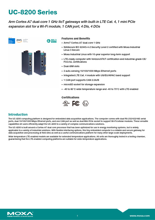
UC-8200SeriesArm Cortex-A7dual-core1GHz IIoT gateways with built-in LTE Cat.4,1mini PCIe expansion slot for a Wi-Fi module,1CAN port,4DIs,4DOsFeatures and Benefits•Armv7Cortex-A7dual-core1GHz•ISASecure IEC62443-4-2Security Level2certified with Moxa IndustrialLinux3Secure•Moxa Industrial Linux with10-year superior long-term support•LTE-ready computer with Verizon/AT&T certification and industrial-grade CE/FCC/UL certifications•Dual-SIM slots•2auto-sensing10/100/1000Mbps Ethernet ports•Integrated LTE Cat.4module with US/EU/APAC band support•1CAN port supports CAN2.0A/B•microSD socket for storage expansion•-40to85°C wide temperature range and-40to70°C with LTE enabledCertificationsIntroductionThe UC-8200computing platform is designed for embedded data acquisition applications.The computer comes with dual RS-232/422/485serial ports,dual10/100/1000Mbps Ethernet ports,and one CAN port as well as dual Mini PCIe socket to support Wi-Fi/cellular modules.These versatile capabilities let users efficiently adapt the UC-8200to a variety of complex communications solutions.The UC-8200is built around a Cortex-A7dual core processor that has been optimized for use in energy monitoring systems,but is widely applicable to a variety of industrial solutions.With flexible interfacing options,this tiny embedded computer is a reliable and secure gateway for data acquisition and processing at field sites as well as a useful communications platform for many other large-scale deployments.Wide temperature LTE-enabled models are available for extended temperature applications.All units are thoroughly tested in a testing chamber, guaranteeing that the LTE-enabled computing platforms are suitable for wide-temperature applications.AppearanceUC-8210UC-8220SpecificationsComputerCPU Armv7Cortex-A7dual-core1GHzDRAM2GB DDR3LSupported OS Moxa Industrial Linux1(Debian9,kernel4.4),2027EOLMoxa Industrial Linux31(Debian11,kernel5.10),2031EOLSee /MILStorage Pre-installed8GB eMMCExpansion Slots MicroSD(SD3.0)socket x13OS is selectable via Moxa Computer Configuration System(CCS)for CTO models.For the model names,see the Ordering Information section of thedatasheet PDF file.Computer InterfaceEthernet Ports Auto-sensing10/100/1000Mbps ports(RJ45connector)x2 Serial Ports RS-232/422/485ports x2,software selectable(DB9male) CAN Ports CAN2.0A/B x1(DB9male)Digital Input DIs x4Digital Output DOs x4USB2.0USB2.0hosts x1,type-A connectorsWi-Fi Antenna Connector UC-8220Models:RP-SMA x2Cellular Antenna Connector UC-8220Models:SMA x2GPS Antenna Connector UC-8220Models:SMA x1Expansion Slots UC-8220-T-LX:mPCIe slot x2UC-8220-T-LX US/EU/AP Models:mPCIe slot x1SIM Format UC-8220Models:NanoNumber of SIMs UC-8220Models:2Buttons Programmable buttonTPM TPM v2.0Ethernet InterfaceMagnetic Isolation Protection 1.5kV(built-in)Security FunctionsHardware-based Security TPM2.0Hardware Root of Trust Secure BootIntrusion Detection Host-based Intrusion DetectionSecurity Tools Security Diagnostic ToolSecurity Event AuditingSecure UpdateDisk Protection LUKS Disk EncryptionRecovery One-step recovery to the last known secure stateDual-system design with automatic failbackReliability Network Keep AliveNetwork Failover and FailbackSerial InterfaceBaudrate300bps to921.6kbpsData Bits7,8Stop Bits1,2Parity None,Even,Odd,Space,MarkFlow Control RTS/CTS,XON/XOFFADDC(automatic data direction control)for RS-485RTS Toggle(RS-232only)Console Port1x4-pin header to DB9console portRS-232TxD,RxD,RTS,CTS,DTR,DSR,DCD,GNDRS-422Tx+,Tx-,Rx+,Rx-,GNDRS-485-2w Data+,Data-,GNDCAN InterfaceNo.of Ports1Connector DB9maleBaudrate10to1000kbpsIndustrial Protocols CAN2.0ACAN2.0BIsolation2kV(built-in)Signals CAN_H,CAN_L,CAN_GND,CAN_SHLD,CAN_V+,GNDDigital InputsConnector Screw-fastened Euroblock terminalDry Contact Off:openOn:short to GNDIsolation3K VDCSensor Type Wet contact(NPN)Dry contactWet Contact(DI to COM)On:10to30VDCOff:0to3VDCDigital OutputsConnector Screw-fastened Euroblock terminalCurrent Rating200mA per channelI/O Type SinkVoltage24VDC nominal,open collector to30VDCCellular InterfaceCellular Standards LTE Cat.4Band Options US Models:LTE Band2(1900MHz)/LTE Band4(1700MHz)/LTE Band5(850MHz)/LTE Band13(700MHz)/LTE Band17(700MHz)UMTS/HSPA850MHz/1900MHzCarrier Approval:Verizon,AT&TEU Models:LTE Band1(2100MHz)/LTE Band3(1800MHz)/LTE Band5(850MHz)/LTE Band7(2600MHz)/LTE Band8(900MHz)/LTE Band20(800MHz)UMTS/HSPA850MHz/900MHz/1900MHz/2100MHzAP Models:LTE Band1(2100MHz)/LTE Band3(1800MHz)/LTE Band5(850MHz)/LTE Band7(2600MHz)/LTE Band8(900MHz)/LTE Band28(700MHz)UMTS/HSPA850MHz/900MHz/1900MHz/2100MHzReceiver Types GPS/GLONASS/GalileoState-of-the-art GNSS solutionAccuracy Position:2.0m@CEP50Acquisition Hot starts:1.1secCold starts:29.94secSensitivity Cold starts:-145dBmTracking:-160dBmTime Pulse0.25Hz to10MHzLED IndicatorsSystem Power x2Programmable x1SIM card indicator x1Wireless Signal Strength Cellular/Wi-Fi x6Power ParametersNo.of Power Inputs Redundant dual inputsInput Voltage12to48VDCPower Consumption10WInput Current0.8A@12VDCReliabilityAlert Tools External RTC(real-time clock)Automatic Reboot Trigger External WDT(watchdog timer)Physical CharacteristicsDimensions UC-8220Models:141.5x120x39mm(5.7x4.72x1.54in)UC-8210Models:141.5x120x27mm(5.7x4.72x1.06in)141.5x120x27mm(5.7x4.72x1.06in)Weight UC-8210Models:560g(1.23lb)UC-8220Models:750g(1.65lb)Housing SECCMetalIP Rating IP30Installation DIN-rail mountingWall mounting(with optional kit)Environmental LimitsOperating Temperature-40to70°C(-40to158°F)Storage Temperature(package included)-40to85°C(-40to185°F)Ambient Relative Humidity5to95%(non-condensing)Shock IEC60068-2-27Vibration2Grms@IEC60068-2-64,random wave,5-500Hz,1hr per axis(without USB devicesattached)Standards and CertificationsEMC EN55032/35EN61000-6-2/-6-4EMI CISPR32,FCC Part15B Class AEMS IEC61000-4-2ESD:Contact:4kV;Air:8kVIEC61000-4-3RS:80MHz to1GHz:10V/mIEC61000-4-4EFT:Power:2kV;Signal:1kVIEC61000-4-6CS:10VIEC61000-4-8PFMFIEC61000-4-5Surge:Power:0.5kV;Signal:1kV Industrial Cybersecurity IEC62443-4-1IEC62443-4-2Hazardous Locations Class I Division2ATEXIECExCarrier Approvals VerizonAT&TSafety UL62368-1EN62368-1Green Product RoHS,CRoHS,WEEEMTBFTime UC-8210-T-LX-S:708,581hrsUC-8220-T-LX:650,836hrsUC-8220-T-LX-US-S/EU-S/AP-S:528,574hrs Standards Telcordia(Bellcore)Standard TR/SRWarrantyWarranty Period5yearsDetails See /warrantyPackage ContentsDevice1x UC-8200Series computerDocumentation1x quick installation guide1x warranty cardInstallation Kit1x DIN-rail kit(preinstalled)1x power jack6x M2.5mounting screws for the cellular module Cable1x console cableDimensions UC-8210UC-8220Ordering Information12UC-8210-T-LX-SDefault:MIL1(-Debian9),2027EOLOrder WithModel UC-8210-T-LX-S(CTO):MIL3(Debian11)Secure/Standard,2031EOLWith MIL3Secure1GHzDual CoreBuilt in––-40to85°CUC-8220-T-LXDefault:MIL1(-Debian9),2027EOLOrder WithModel UC-8220-T-LX(CTO):MIL3(Debian11)Secure/Standard,2031EOLWith MIL3Secure1GHzDual CoreBuilt in Reserved Reserved-40to70°CUC-8220-T-LX-US-SDefault:MIL1(-Debian9),2027EOLOrder WithModel UC-8220-T-LX-US-S(CTO):MIL3(Debian11)Secure/Standard,2031EOLWith MIL3Secure1GHzDual CoreBuilt inUS region LTEmodulepreinstalledReserved-40to70°CUC-8220-T-LX-EU-SDefault:MIL1(-Debian9),2027EOLOrder WithModel UC-8220-T-LX-EU-S(CTO):MIL3(Debian11)Secure/Standard,2031EOLWith MIL3Secure1GHzDual CoreBuilt inEurope regionLTE modulepreinstalledReserved-40to70°CUC-8220-T-LX-AP-SDefault:MIL1(-Debian9),2027EOLOrder WithModel UC-8220-T-LX-AP-S(CTO):MIL3(Debian11)Secure/Standard,2031EOLWith MIL3Secure1GHzDual CoreBuilt inAPAC regionLTE modulepreinstalledReserved-40to70°CUC-8210-T-LX-S(CTO)MIL3(Debian11)Secure orStandard,2031EOLWith MIL3Secure1GHzDual CoreBuilt in––-40to85°CUC-8220-T-LX(CTO)MIL3(Debian11)Secure orStandard,2031EOLWith MIL3Secure1GHzDual Core–Reserved Reserved-40to70°CUC-8220-T-LX-US-S (CTO)MIL3(Debian11)Secure orStandard,2031EOLWith MIL3Secure1GHzDual CoreBuilt inUS region LTEmodulepreinstalledReserved-40to70°C12UC-8220-T-LX-EU-S (CTO)MIL3(Debian11)Secure orStandard,2031EOLWith MIL3Secure1GHzDual CoreBuilt inEurope regionLTE modulepreinstalledReserved-40to70°CUC-8220-T-LX-AP-S (CTO)MIL3(Debian11)Secure orStandard,2031EOLWith MIL3Secure1GHzDual CoreBuilt inAPAC regionLTE modulepreinstalledReserved-40to70°CAccessories(sold separately)Power AdaptersPWR-12150-EU-SA-T Locking barrel plug,12VDC,1.5A,100to240VAC,EU plug,-40to75°C operating temperature PWR-12150-UK-SA-T Locking barrel plug,12VDC,1.5A,100to240VAC,UK plug,-40to75°C operating temperature PWR-12150-USJP-SA-T Locking barrel plug,12VDC1.5A,100to240VAC,US/JP plug,-40to75°C operating temperature PWR-12150-AU-SA-T Locking barrel plug,12VDC,1.5A,100to240VAC,AU plug,-40to75°C operating temperature PWR-12150-CN-SA-T Locking barrel plug,12VDC,1.5A,100to240VAC,CN plug,-40to75°C operating temperature Power WiringCBL-PJTB-10Non-locking barrel plug to bare-wire cableCablesCBL-F9DPF1x4-BK-100Console cable with4-pin connector,1mWi-Fi Wireless ModulesUC-8200-WLAN22-AC Wireless package for UC-8200V2.0or later with Wi-Fi module,2screws,2spacers,1heat sink,1pad AntennasANT-LTEUS-ASM-01GSM/GPRS/EDGE/UMTS/HSPA/LTE,1dBi,omnidirectional rubber-duck antennaANT-LTE-ASM-04BK704to960/1710to2620MHz,LTE omnidirectional stick antenna,4.5dBiANT-LTE-OSM-03-3m BK700-2700MHz,multiband antenna,specifically designed for2G,3G,and4G applications,3m cable ANT-LTE-ASM-05BK704-960/1710-2620MHz,LTE stick antenna,5dBiANT-LTE-OSM-06-3m BK MIMO Multiband antenna with screw-fastened mounting option for700-2700/2400-2500/5150-5850MHzfrequenciesANT-WDB-ARM-02022dBi at2.4GHz or2dBi at5GHz,RP-SMA(male),dual-band,omnidirectional antennaDIN-Rail Mounting KitsUC-8210DIN-rail Mounting Kit DIN-rail mounting kit for UC-8210with4M3screwsUC-8220DIN-rail Mounting Kit DIN-rail mounting kit for UC-8220with4M3screwsWall-Mounting KitsUC-8200Wall-mounting Kit Wall-mounting kit for UC-8200with4M3screws©Moxa Inc.All rights reserved.Updated Jul18,2023.This document and any portion thereof may not be reproduced or used in any manner whatsoever without the express written permission of Moxa Inc.Product specifications subject to change without notice.Visit our website for the most up-to-date product information.。
MOXA UC-8410 8416 8418 8430 硬件用户手册7.0说明书

UC-8410/8416/8418/8430 Hardware User’s ManualEdition 7.0, February 2017/product© 2017 Moxa Inc. All rights reserved.UC-8410/8416/8418/8430Hardware User’s ManualThe software described in this manual is furnished under a license agreement and may be used only in accordance withthe terms of that agreement.Copyright Notice© 2017 Moxa Inc. All rights reserved.TrademarksThe MOXA logo is a registered trademark of Moxa Inc.All other trademarks or registered marks in this manual belong to their respective manufacturers.DisclaimerInformation in this document is subject to change without notice and does not represent a commitment on the part of Moxa.Moxa provides this document as is, without warranty of any kind, either expressed or implied, including, but not limited to, its particular purpose. Moxa reserves the right to make improvements and/or changes to this manual, or to the products and/or the programs described in this manual, at any time.Information provided in this manual is intended to be accurate and reliable. However, Moxa assumes no responsibility for its use, or for any infringements on the rights of third parties that may result from its use.This product might include unintentional technical or typographical errors. Changes are periodically made to the information herein to correct such errors, and these changes are incorporated into new editions of the publication.Technical Support Contact Information/supportMoxa AmericasToll-free: 1-888-669-2872 Tel: +1-714-528-6777 Fax: +1-714-528-6778Moxa China (Shanghai office) Toll-free: 800-820-5036Tel: +86-21-5258-9955 Fax: +86-21-5258-5505Moxa EuropeTel: +49-89-3 70 03 99-0 Fax: +49-89-3 70 03 99-99Moxa Asia-PacificTel: +886-2-8919-1230 Fax: +886-2-8919-1231Moxa IndiaTel: +91-80-4172-9088 Fax: +91-80-4132-1045Table of Contents1.Introduction ...................................................................................................................................... 1-1Overview ........................................................................................................................................... 1-2 Package Checklist ............................................................................................................................... 1-2 Product Features ................................................................................................................................ 1-2 Product Hardware Specifications ........................................................................................................... 1-3 2.Appearance and Dimensions ............................................................................................................. 2-1Appearance ........................................................................................................................................ 2-2 Dimensions ........................................................................................................................................ 2-6 Hardware Block Diagrams .................................................................................................................. 2-10 LED Indicators .................................................................................................................................. 2-12 Reset Button .................................................................................................................................... 2-12 Real Time Clock ................................................................................................................................ 2-12 3.Mounting Options .............................................................................................................................. 3-1Wall or Cabinet Mounting ..................................................................................................................... 3-2 DIN-Rail Mounting .............................................................................................................................. 3-2 4.Hardware Connection Description ..................................................................................................... 4-1Wiring Requirements ........................................................................................................................... 4-2 Connecting the Power ......................................................................................................................... 4-2 Connecting to VGA Monitors (UC-8430 only) .......................................................................................... 4-3 Connecting to the Network ................................................................................................................... 4-3 Connecting to a Serial Device ............................................................................................................... 4-4 Connecting to a CAN Device ................................................................................................................. 4-4 Connecting to a Speaker or a Headphone (UC-8430 only) ........................................................................ 4-4 Connecting to the Console Port ............................................................................................................. 4-5 CompactFlash .................................................................................................................................... 4-6 USB .................................................................................................................................................. 4-7 DI/DO ............................................................................................................................................... 4-7 Digital Input Wiring ..................................................................................................................... 4-7Digital Output Wiring ................................................................................................................... 4-8 A.Regulatory Approval Statements ....................................................................................................... A-11IntroductionThank you for purchasing the Moxa UC-8410/8416/8418/8430 RISC-based ready-to-run embedded computer. The UC-8410/8416/8418/8430 feature 8 RS-232/422/485 serial ports, 3 10/100 Mbps Ethernet ports, digital input and digital output channels, switching ports, and CompactFlash and USB ports for adding additional memory. All of these features make the UC-8410/8416/8418/8430 ideal for your embedded applications. Note, too, that the UC-8430 comes with 2 VGA outputs, offering dual display connections for field site monitoring.This manual introduces the hardware of the UC-8410/8416/8418/8430 embedded computers. After a brief introduction of the hardware features, we focus on installing and configuring the hardware.The following topics are covered in this chapter:❒Overview❒Package Checklist❒Product Features❒Product Hardware SpecificationsOverviewThe UC-8410/8416/8418/8430 features 8 RS-232/422/485 serial ports, 3 10/100 Mbps Ethernet ports, 4digital input channels and 4 digital output channels (12 digital input channels and 12 digital output channels for the UC-8418), 8 10/100 Mbps switch ports (UC-8416 only), a CompactFlash slot for flash disk expansion, and2 USB ports (6 USB ports for UC-8430) for adding additional memory (such as a USB flash drive).The UC-8410/8416/8418/8430 uses an Intel XScale IXP435 533 MHz RISC CPU. Unlike the X86 CPU, which uses a CISC design, the IXP435's RISC design architecture and modern semiconductor technology provide the UC-8410/8416/8418/8430 with a powerful computing engine and communication functions, but withoutgenerating a lot of heat. The built-in 16 MB (32 MB for UC-8430) NOR Flash ROM and 256 MB SDRAM give you enough memory to run your application software directly on the UC-8410/8416/8418/8430. Since the dual LAN ports are built into the IXP435 CPU, the UC-8410/8416/8418/8430 is good solution for network securityapplications.Package ChecklistAll models of the UC-8410/8416/8418/8430 series are shipped with the following items:• 1 UC-8410/8416/8418/8430 series embedded computer•Wall-mounting kit•DIN-Rail mounting kit•Quick installation guide (printed)•Document & software CD•Cross-over Ethernet cable•CBL-4PINDB9F-100: 4-pin pin header to DB9 female console port cable, 100 cm•Universal power adaptor•Warranty cardNOTE: Please notify your sales representative if any of the above items are missing or damaged.Product Features•Intel XScale IXP435 533 MHz processor•On-board 256 MB DDR2 SDRAM (max. 512 MB)•16 MB (32 MB for UC-8430) NOR Flash onboard to store OS, 32 MB NAND Flash onboard for data storage •8 RS-232/422/485 serial ports• 4 digital input and 4 digital output channels (12 digital input and 12 digital output channels for UC-8418) •Dual displays for field site monitoring (UC-8430 only)•Three 10/100 Mbps Ethernet ports• 2 USB 2.0 hosts (6 for UC-8430) for mass storage devices•8 10/100 Mbps switch ports (UC-8416 only)• 2 CANbus ports (UC-8418 only)•CompactFlash socket for storage expansion•Ready-to-run Linux or Windows CE 6.0 platform•DIN-Rail or wall mounting installation•Robust, fanless designProduct Hardware SpecificationsComputerCPU: Intel XScale IXP435, 533 MHzOS (pre-installed): Linux or Windows CE 6.0DRAM: 256 MB DDR2 SDRAM onboard (512 MB max.)SRAM: 256 KB, battery backupFlash:• NOR Flash onboard to store OS> UC-8410/8416/8418: 16 MB> UC-8430: 32 MB• 32 MB NAND Flash onboard to store dataExpansion Bus: PCI/104 onboardUSB: USB 2.0 compliant hosts, type A connector• UC-8410/8416/8418: 2 hosts• UC-8430: 6 hostsStorageStorage Expansion: CompactFlash socketOther Peripherals (UC-8430 only)Audio: SM502 chip with line-in/out interfaceDisplay (UC-8430 only)Graphics Controller: SM502 chipDisplay Interface: 15-pin D-Sub connector x 2Resolution: CRT display mode with pixel resolution up to 1024 x 768Ethernet InterfaceLAN: 3 auto-sensing 10/100 Mbps ports (RJ45)Switch Ports: 8 10/100 Mbps unmanaged ports (UC-8416 only)Magnetic Isolation Protection: 1.5 KV built-inSerial InterfaceSerial Standards: 8 RS-232/422/485 ports, software-selectable (8-pin RJ45)Console Port: RS-232 (TxD, RxD, GND), 4-pin header output (115200, n, 8, 1)Serial Communication ParametersData Bits: 5, 6, 7, 8Stop Bits: 1, 1.5, 2Parity: None, Even, Odd, Space, MarkFlow Control: RTS/CTS, XON/XOFF, ADDC® (automatic data direction control) for RS-485Baudrate: 50 bps to 921.6 Kbps (supports non-standard baudrates; see user's manual for details) Serial SignalsRS-232: TxD, RxD, DTR, DSR, RTS, CTS, DCD, GNDRS-422: TxD+, TxD-, RxD+, RxD-, GNDRS-485-4w: TxD+, TxD-, RxD+, RxD-, GNDRS-485-2w: Data+, Data-, GNDDigital InputInput Channels: source type• UC-8410/8416/UC8430: 4 channels• UC-8418: 12 channelsInput Voltage: 0 to 30 VDCDigital Input Levels for Dry Contacts:• Logic level 0: Close to GND• Logic level 1: OpenDigital Input Levels for Wet Contacts:• Logic level 0: +3V max.• Logic level 1: +10V to +30V (COM to DI)Connector Type: 10-pin screw terminal block (4 points, COM, GND) Isolation: 3 KV optical isolationDigital OutputOutput Channels: sink type• UC-8410/8416/UC8430: 4 channels• UC-8418: 12 channelsOutput Current: Max. 200 mA per channelOn-state Voltage: 24 VDC nominal, open collector to 30 VConnector Type: 10-pin screw terminal block (4 points, GND)Isolation: 3 KV optical isolationCANbus Communication (UC-8418 only)Interface: Dual optically isolated CAN2.0A/2.0B compliant portsCAN Controller: Phillips SJA1000TSignals: CAN-H, CAN-LIsolation: 2 KV digital isolationSpeed: 10 Kbps to 1 MbpsConnector Type: DB9 maleLEDsSystem: Power, Ready, Storage, Battery for SRAMLAN: 10M/Link x 2, 100M/Link x 2 (on connector)Serial: TxD x 8, RxD x 8Reset Button: Supports "Reset to Factory Default"Physical CharacteristicsHousing: SECC sheet metal (1 mm)Weight: 1 kgDimensions:UC-8410: 200 x 37 x 120 mm (7.87 x 1.46 x 4.72 in)UC-8416/8418: 200 x 57 x 120 mm (7.87 x 2.24 x 4.72 in)Mounting: DIN-Rail, wallEnvironmental LimitsOperating Temperature:Standard Models: -10 to 60°C (14 to 140°F)Wide Temp. Models: -40 to 75°C (-40 to 167°F)Operating Humidity: 5 to 95% RHStorage Temperature:Standard Models: -20 to 75°C (-4 to 167°F)Wide Temp. Models: -40 to 85°C (-40 to 185°F)Anti-vibration: 2 g rms @ IEC-68-2-34, random wave, 5-500 Hz, 1 hr per axis Anti-shock: 20 g @ IEC-68-2-27, half sine wave, 11 msPower RequirementsInput Voltage: 12 to 48 VDC (3-pin terminal block)Power Consumption: 15 W• 310 mA @ 48 VDC• 625 mA @ 24 VDC• 1350 mA @ 12 VDCRegulatory ApprovalsEMC: CE (EN55032 Class B, EN55024-4-2, EN55024-4-3,EN55024-4-4), FCC (Part 15 Subpart B, Class B)Safety: UL/cUL (UL60950-1), CCC (GB9254, GB 17625.1), LVD (EN60950) ReliabilityAlert Tools: Built-in buzzer and RTC (real-time clock)Automatic Reboot Trigger: Built-in WDT (watchdog timer)WarrantyWarranty Period: 5 yearsDetails: See /warrantyNote: The Hardware Specifications apply to the embedded computer unit itself, but not to accessories. In particular, the wide temperature specification does not apply to accessories such as the power adaptor and cables.2Appearance and DimensionsThe following topics are covered in this chapter:❒Appearance❒Dimensions❒Hardware Block Diagrams❒LED Indicators❒Reset Button❒Real Time ClockUC-8410/8416/8418/8430 Hardware Appearance and DimensionsAppearanceUC-8410 Rear ViewUC-8410 Top ViewUC-8410 Front ViewUC-8416 Top ViewUC-8416 Front ViewUC-8418 Top ViewUC-8418 Front ViewUC-8430 Top ViewUC-8430 Front ViewDimensions UC-8410(Unit=mm)(Unit=mm)(Unit=mm)(Unit=mm)Hardware Block DiagramsThe following block diagram shows the layout of the UC-8410/8416/8418/8430’s internal components.UC-8410UC-8416UC-8418UC-8430LED IndicatorsThe UC-8410/8416/8418/8430 has 14 LED indicators on the top panel. Refer to the following table for information about each LED. LED Name Color Meaning Power Green Power is on.Off No power input or any other power error. Ready GreenSystem is ready.OffOS boot up failure or other system initialization error. StorageYellow (not blinking)CF card inserted.Yellow (blinking) Data is being read or written. OffNo CF card inserted. Battery Red (blinking) Battery is recharging. Off Battery is normal.TX 1-8 Green Data is being sent through the serial port. Off Data is not being transmitted.RX 1-8Yellow Data is being received through the serial port. OffData is not being received.Reset ButtonThe button labeled Reset returns the UC-8410/8416/8418/8430 to its factory default configuration.Press the Reset button continuously for at least 5 seconds to load the factory default configuration . After the factory default configuration has been loaded, the system will reboot automatically. The Ready LED will blink on and off for the first 5 seconds, and then maintain a steady glow once the system has rebooted. We recommend that you only use this function if the software is not working properly and you want to load factory default settings. To reset an embedded system, always use the software reboot command />reboot to protect the integrity of data being transmitted or processed.Real Time ClockThe UC-8410/8416/8418/8430’s real time clock is powered by a lithium battery. We strongly recommend that you do not replace the lithium battery without help from a qualified Moxa support engineer. If you need to change the battery, contact the Moxa RMA service team.3Mounting OptionsThe following topics are covered in this chapter:❒Wall or Cabinet Mounting❒DIN-Rail MountingUC-8410/8416/8418/8430 Hardware Mounting OptionsWall or Cabinet MountingThe two metal brackets that come standard with the UC-8410/8416/8418/8430 are used to attach the UC-8410/8416/8418/8430 to a wall or the inside of a cabinet. First, use two screws per bracket to attach the brackets to the bottom of the UC-8410/8416/8418/8430 (Fig. A). Next, use two screws per bracket to attach the UC-8410/8416/8418/8430 to a wall or cabinet (Fig. B).Figure A: UC-8410/8416/8418/8430 Embedded Computer—Wall Mounting Brackets (bottom view)Figure B: UC-8410/8416/8418/8430 Embedded Computer—Wall Mounting Brackets (top view)DIN-Rail MountingAn aluminum DIN-Rail attachment plate is included with the product. If you need to reattach the DIN-Rail attachment plate to the UC-8410/8416/8418/8430, make sure the stiff metal spring is situated towards the top, as shown in the following figures.STEP 1: Insert the top of the DIN-Rail into the slot just below the stiff metal spring.STEP 2: The DIN-Rail attachment unit will snap into place as shown below.To remove the UC-8410/8416/8418/8430 from the DIN-Rail, simply reverse Steps 1 and 2.4 Hardware Connection DescriptionThis section describes how to connect the UC-8410/8416/8418/8430 to serial devices for first time testing purposes.The following topics are covered in this chapter:❒Wiring Requirements❒Connecting the Power❒Connecting to VGA Monitors (UC-8430 only)❒Connecting to the Network❒Connecting to a Serial Device❒Connecting to a CAN Device❒Connecting to a Speaker or a Headphone (UC-8430 only)❒Connecting to the Console Port❒CompactFlash❒USB❒DI/DODigital Input WiringDigital Output WiringWiring RequirementsYou should also observe the following common wiring rules:• Use separate paths to route wiring for power and devices. If power wiring and device wiring paths mustcross, make sure the wires are perpendicular at the intersection point.NOTE: Do not run signal or communication wiring and power wiring in the same wire conduit. To avoid interference, wires with different signal characteristics should be routed separately.• You can use the type of signal transmitted through a wire to determine which wires should be kept separate.The rule of thumb is that wiring that shares similar electrical characteristics can be bundled together. • Keep input wiring and output wiring separate.•Where necessary, we strongly recommend that you label wiring to all devices in the system.Connecting the PowerThe UC-8410/8416/8418/8430 has a 3-pin terminal block for a 12 to 48 VDC power input.The following figures show how the power input interface connects to external power source. If the power is properly supplied, t the Ready LED will illuminate with a solid green color after 30 to 60 seconds have passed.Grounding the UC-8410/8416/8418/8430Grounding and wire routing help limit the effects of noise due to electromagnetic interference (EMI). Run the ground connection from the ground screw to the grounding surface prior to connecting devices.SG: The Shielded Ground (sometimes called Protected Ground ) contact is the right most contact of the 3-pin power terminal block connector when viewed from the angle shown here. Connect the SG wire to an appropriate grounded metal surface.Connecting to VGA Monitors (UC-8430 only)The UC-8430 comes with two D-sub 15-pin female connectors on the rear panel to connect two VGA monitors. To ensure that the monitor image remains clear, be sure to tighten the monitor cable after connecting it to the UC-8430. The pin assignments of the VGA connectors are shown below. DB15 Female ConnectorPin No. Signal DefinitionPin No.Signal Definition 1 Red 9 VCC 2 Green 10 GND 3 Blue 11 NC4 NC 12 DDC2B Data 5GND 13 HSYNC 6 GND 14 VSYNC 7 GND 15 DDC2B Clock 8GNDConnecting to the NetworkConnect one end of the Ethernet cable to one of the UC-8410/8416/8418/8430’s 10/100M Ethernet ports (8-pin RJ45) and the other end of the cable to the Ethernet network. If the cable is properly connected, the UC-8410/8416/8418/8430 will indicate a valid connection to the Ethernet in the following ways:The lower right corner LED indicator maintains a solid green colorwhen the cable is properly connected to a 100 Mbps Ethernet network. The LED will flash on and off when Ethernet packets are being transmitted or received. Pin Signal 1 ETx+ 2 ETx- 3 ERx+ 4 – 5 – 6 ERx- 7 – 8–The lower left corner LED indicator maintains a solid orange color when the cable is properly connected to a 10 Mbps Ethernet network. The LED will flash on and off when Ethernet packets are being transmitted or received.The UC-8416 has 8 10/100 Mbps switch ports. The LED indicators and pin assignments are exactly the same as the Ethernet ports.Connecting to a Serial DeviceUse properly wired serial cables to connect the UC-8410/8416/8418/8430 to serial devices. TheUC-8410/8416/8418/8430’s serial ports (P1 to P8) use 8-pin RJ45 connectors. The ports can be configured by software for RS-232, RS-422, or 2-wire RS-485. The precise pin assignments are shown in the following table:Pin RS-232 RS-422/ RS-485-4wRS-485-2w1DSR – – 2 RTS TXD+ – 3 GND GND GND 4 TXD TXD- – 5 RXD RXD+ Data+ 6DCD RXD-Data- 7 CTS – – 8DTR––Connecting to a CAN DeviceCAN Ports (UC-8418 only)The UC-8418 has 2 CAN ports for connecting CAN devices. The CAN ports (CAN1 and CAN2) use DB9 male connectors. The pin assignments are shown in the following table:Pin CAN 1 – 2 CAN-L 3– 4 – 5 – 6 – 7 CAN-H 8–Connecting to a Speaker or a Headphone (UC-8430 only)The UC-8430 comes with audio input and output interfaces for connecting a microphone and speaker or headphones. See the following figure for details.Connecting to the Console PortThe UC-8410/8416/8418/8430’s console port is a 4-pin pin header RS-232 port. Refer to the following figure for console port cable pin assignments. Serial Console Port and PinoutsSerial Console CablePinSignal1TxD 2 RxD 3 NC 4 GNDThe console port is located blow the CF card socket. Use a screwdriver to remove the two screws holding the cover to the embedded computer’s housing.Refer to the following figure for the location of the console port.CompactFlashThe UC-8410/8416/8418/8430 provides one CompactFlash slot that supports CompactFlash type I/II cardexpansion. Currently, Moxa provides a CompactFlash card for storage expansion. Be sure of power off thecomputer before inserting or removing the CompactFlash card.See the following description for CompactFlash card installation instructions.The CF cover is located on the back of the UC-8410/8416/8418/8430. Use a screwdriver to remove the cover and access the slot. See the following figure for the locations of the CF socket.If you need device drivers for other kinds of mass storage cards, contact Moxa for information on how to initiatea cooperative development project.USBThe UC-8410/8416/8418/8430 provides two or six USB 2.0 hosts. The USB hosts now support adding USBstorage devices.DI/DOThe UC-8410/8416/8430 have 4-ch digital outputs and 4-ch digital inputs, while the UC-8418 has 12-ch digital inputs and 12-ch digital outputs. The pinouts for the I/O are shown in the following figures:Digital Input WiringDry ContactWet ContactNote: If are using wet contacts, you must connect “COM” to power. Digital Output WiringA Regulatory Approval StatementsThis device complies with part 15 of the FCC Rules. Operation is subject to the following two conditions: (1) This device may not cause harmful interference, and (2) this device must accept any interference received, including interference that may cause undesired operation.。
Vigor2920 系

Vigor2920 系列雙WAN安全防護路由器快速安裝手冊版本: 1.0韌體版本: V3.3.3.1日期: 19/07/2010因手冊更新無法及時通知用戶,請隨時連上居易網站,取得最新的手冊內容。
版權資訊版權聲明© 2010版權所有,翻印必究。
此出版物所包含資訊受版權保護。
未經版權所有人書面許可,不得對其進行拷貝、傳播、轉錄、摘錄、儲存到檢索系統或轉譯成其他語言。
交貨以及其他詳細資料的範圍若有變化,恕不預先通知。
商標本手冊內容使用以下商標:z Microsoft為微軟公司註冊商標z Windows視窗系列,包括Windows 95, 98, Me, NT, 2000, XP 以及其Explorer均屬微軟公司商標z Apple以及Mac OS均屬蘋果電腦公司的註冊商標z其他產品則為各自生產廠商之註冊商標安全說明和保障安全說明z在設置前請先閱讀安裝說明。
z由於路由器是複雜的電子產品,請勿自行拆除或是維修本產品。
z請勿自行打開或修復路由器。
z請勿把路由器置於潮濕的環境中,例如浴室。
z請將本產品放置在足以遮風避雨之處,適合溫度在攝氏5度到40度之間。
z請勿將本產品暴露在陽光或是其他熱源下,否則外殼以及零件可能遭到破壞。
z請勿將LAN網線置於戶外,以防電擊危險。
z請將本產品放置在小孩無法觸及之處。
z若您想棄置本產品時,請遵守當地的保護環境的法律法規。
保固自使用者購買日起二年內為保固期限,請將您的購買收據保存二年,因為它可以證明您的購買日期。
當本產品發生故障乃導因於製作及(或)零件上的錯誤,只要使用者在保固期間內出示購買證明,居易科技將採取可使產品恢復正常之修理或更換有瑕疵的產品(或零件),且不收取任何費用。
居易科技可自行決定使用全新的或是同等價值且功能相當的再製產品。
下列狀況不在本產品的保固範圍內:(1)若產品遭修改、錯誤(不當)使用、不可抗力之外力損害,或不正常的使用,而發生的故障;(2) 隨附軟體或是其他供應商提供的授權軟體;(3) 未嚴重影響產品堪用性的瑕疵。
OV系列单芯片CMOS摄像机中文资料
电视机,视频监视器和其他75欧姆终端输入的视频设
备。OV7910 / OV7410 / OV7411视频摄像机是低功耗设
计,仅需要5V 直流供电。这两个产品非常合适于小体
感光阵列
NTSC:510*492像素
PAL:628*582像素
靶面尺寸
NTSC:4.69*3.54毫米
PAL:5.78*4.19毫米
单芯片1/3英寸
视频摄像机
全电视信号输
出:NTSC/ PAL 或
S-视频
分量电视信号
输出:RGB 或 YUV
灵敏度提升
(+18Db)/ AGC
关闭时
自动暴光控制
/ 自动增益控制/
自动白平衡
外部桢同步输
入
孔阑校正
视频会议
可视电视
视频电子邮件
PC 电脑眼 玩具 保安监视 医疗仪器 汽车尾视
VTO-P 视频峰值电平
-
2.3
2.4
-
VTO-B 视频黑电平
-
0.7
1.2
-
VSYNC 视频同步脉冲
-
0.7
0.4
-
幅度
RO 视频输出负载
75
75
单位
V V V Ohm
2. SCCB 总线 OV7910/OV7410/OV7411中的许多功能是设置寄存器都可以通过 SCCB 高
速 串行接口操作。通过将 SBB 管脚(管脚34)和 VDD 之间一个10K 电阻,即可 允许 SCCB 接口。当 SCCB 操作允许时(SBB=1),OV7910/OV7410/OV7411 图像传感器就以从设备方式工作,支持7位地址/数据和400K 位/秒的串行传输 速度。每一个字节,第一位是最高位,读写控制位是第一字节的最低位。协议
莫加 UC 系列产品说明书

Entry-level Arm-based 64-bit ComputersDual-core, 2-GB RAMCompact Dual-core, 2-GB RAM Built-in LTEValue-added Arm-based 64-bit ComputersQuad-core, 4-GB RAMQuad-core, 4-GB RAM5G/CAN/serial IsolationBuilt-in LTEMoxa Industrial LinuxMoxa's Debian-based industrial-grade stable Linux distribution for long-term projectsFeatures and Benefits5Debian-based distribution that can use all standard Debian packages5Developed as per IEC 62443-4-1 and compliant with IEC 62443-4-2 industrialcybersecurity standards (Moxa Industrial Linux 3 Secure)5Long-term support until 2027 for Moxa Industrial Linux 1 and 2031 for MoxaIndustrial Linux 35Wireless connection management utility with automatic network keep alive andfailover5Ready-to-use APIs and library to ease access to hardware and I/O interfaces5Crash-free robust file system5Over-the air (OTA) software updatesWireless-ready Arm-based 32-bit Computers Built-in cellular or Wi-Fi module, RF type approvals, and carrier approvalsBuilt-in LTE Cat.1Built-in LTECat.1 and Wi-FiBuilt-in LTECat.1 and Wi-FiBuilt-in LTECat.4 with Wi-Fi expansion1. Wireless module is built-in. Refer to the Wireless Connection and Expansion Modules section for details.2. Wireless module must be purchased separately. Refer to the Wireless Connection and Expansion Modules section for details.1 mPCIe for cellular/Wi-Fi1 mPCIe forcellular/Wi-Fi1 mPCIe forcellular/Wi-Fi1 mPCIe forcellular/Wi-Fi1 mPCIe for cellular 1mPCIe for Wi-Fi1 mPCIe forcellular/Wi-FiArm-based 32-bit Computers With Wireless Options Flexibility to add cellular or Wi-Fi capability when needed1. Wireless module must be purchased separately. Refer to the Wireless Connection and Expansion Modules section for details.1 LAN,1 serial2 LAN 2 LAN,2 serial2 LAN,2 serial2 LAN,4 serial2 LAN,4 serial2 LAN,1 serial2 LAN,2 serial3 LAN,8 serialStandard Arm-based 32-bit Computers Low power consumption and small form factorWireless Connectivity and Expansion Modules* Details of cellular and Wi-Fi support with a list of wireless accessory models* Antennas must be purchased separatelyLast updated: Aug. 15, 2023. All specifications are subject to change without notice.。
电脑耗材

台 个 个 套 套 个 套 套 个 个 块 根 个 米
1 3 1 1 1 1 1 1 1 5 2 4 273 419
电脑配件库存状况表
序号 01 010001 010002 02 020001 020002 02000304 04 040001 040002 05 050001 050002 050003 050004 050005 050006 050007 050008 06 060001 07 070001 070002 070003 070004 070005 070006 070007 070008 070009 08 080001 080002 080003 080004 080005 09 090001 090002 10 100001 100002 100003 11 110001 110002 110003 110004 12 120001 名称 电源 SUPERMICRO PWS-865-PQ电源 SUPERMICRO SP650-RP电源 CPU E5410 CPU INTEL i7 950 CPU INTEL i7 970 CPU 硬盘 SATA 硬盘 500G SATA 硬盘 1TB SATA 硬盘 2TB 数帅移动网盘 主板 X58A-UD3R主板 X7DWA-N主板 散热器 S90F 散热风扇 cooler master散热器 黄铜色散热器 Bushless风扇 V12内存散热器 D39267-002散热器 S2N-6FMCS-L7-GP散热器 S2N-PLMH6-07-GP散热器 刻录机 DVR-219CH刻录机 陈列卡 3220阵列卡 3300阵列卡 4320阵列卡 8300阵列卡 8350阵列卡 1204阵列卡 39160SCSI卡 3860QSCSI卡 5K0CT05501ML阵列线 网卡 Lopstar TE-100TXE Rev 1.3网卡 Qxcomm 56K网卡 PC2-X双口网卡 897654双口网卡 0H092P双网卡 显示器 戴尔2211显示器 戴尔2311显示器 软件 雷特字幕 江民杀毒软件 FreeEdit DV LE 2.0编辑软件 鼠标键盘 戴尔键盘 戴尔鼠标 雷特鼠键套装 DELL无线鼠标 鼠标垫 机箱 SC733TQ-665B机箱 数量 个 个 个 个 个 块 块 块 套 块 块 个 个 个 个 个 个 个 个 台 块 块 块 块 块 块 块 块 根 块 块 块 块 块 台 台 套 套 套 个 个 套 个 个 台 1 2 1 4 0 1 36 0 1 4 1 1 3 2 8 2 2 1 7 0 1 3 32 1 4 2 1 1 2 1 1 1 3 1 1 5 23 2 1 3 0 4 1 40 14 备注
监控摄像头的报价
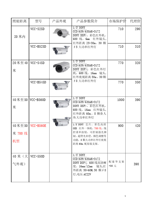
照射距离 型号产品外观 产品参数简介 市场保护价 代理价20米内VCC-525D 1/3'SONY CCD(639/638AK+3172 SONY DSP),彩色红外机,600线,6mm 红外镜头,红外距离25-30m,30颗∮5大功率红外灯 710 290 VCC-B525D710 310 20米至40米 VCC-545D 1/3'SONYCCD(639/638AK+3172SONY DSP),彩色红外灯机,600线,16mm 镜头,红外夜视距离50m ,30颗∮8大功率红外灯 770 320 VCC-B545D770 350 40米至50米VCC-B560D1/3'SONY CCD(639/638AK+3172 SONY DSP),彩色红外机,600线,16mm 红外镜头,红外距离60m ,8颗食人鱼大功率红外灯1000 390 40米至50米700线机型 VCC-B560E 1/3'SONY 芯片,彩色高清OSD 红外一体机,700线,线控菜单按钮,可控制强光抑制、超背光补偿、颜色调整等功能,8颗大功率红外灯夜视距离60m.配原装支架。
900 42040米(大气外观) VCC-550D1/3'SONY CCD(639/638AK+3172 SONY DSP),600线高清晰度,16mm/12mm 镜头,红外距离50-60M,30颗∮8灯,电压AC22V 配豪华支架+30元390700线版本 VCC-B550E1/3'SONY CCD,700线高清晰度,16mm/12mm 镜头,30颗白光灯照射距离30-40M,电压AC22V配豪华支架+30元 46050米至80米V VCC-588DZ1/3'SONY CCD(639/638AK+3172 SONY DSP),彩色变倍红外机,600线,9-22mm 变焦镜头,红外距离50-80m,108颗红外灯 1250 510 650线版本 VCC-588KZ1/3'SONY CCD,宽动态高清OSD 红外变倍摄像机,650线,线控菜单按钮,可控制强光抑制、宽动态功能、颜色调整等功能,内置9-22mm 手动变倍镜头.红外夜视距离50-80m。
MMSZ4xxxT1G系列和SZMMSZ4xxxT1G系列零点电阻电源器件的商品说明书

MMSZ4686T1G MMSZ4686T1G.MMSZ4xxxT1G Series, SZMMSZ4xxxT1G Series Zener Voltage Regulators 500 mW, Low I ZT SOD−123 Surface MountThree complete series of Zener diodes are offered in the convenient, surface mount plastic SOD−123 package. These devices provide a convenient alternative to the leadless 34−package style.Features•500 mW Rating on FR−4 or FR−5 Board•Wide Zener Reverse V oltage Range − 1.8 V to 43 V•Low Reverse Current (I ZT) − 50 m A•Package Designed for Optimal Automated Board Assembly •Small Package Size for High Density Applications•ESD Rating of Class 3 (>16 kV) per Human Body Model•SZ Prefix for Automotive and Other Applications Requiring Unique Site and Control Change Requirements; AEC−Q101 Qualified and PPAP Capable•These Devices are Pb−Free and are RoHS Compliant*Mechanical Characteristics:CASE:V oid-free, transfer-molded, thermosetting plastic case FINISH:Corrosion resistant finish, easily solderableMAXIMUM CASE TEMPERATURE FOR SOLDERING PURPOSES: 260°C for 10 SecondsPOLARITY:Cathode indicated by polarity band FLAMMABILITY RATING:UL 94 V−0MAXIMUM RATINGSRating Symbol Max Units Total Power Dissipation on FR−5 Board,(Note 1) @ T L = 75°CDerated above 75°C P D5006.7mWmW/°CThermal Resistance, (Note 2) Junction−to−Ambient R q JA340°C/WThermal Resistance, (Note 2) Junction−to−Lead R q JL150°C/WJunction and Storage Temperature Range T J, T stg−55 to+150°CStresses exceeding those listed in the Maximum Ratings table may damage the device. If any of these limits are exceeded, device functionality should not be assumed, damage may occur and reliability may be affected.1.FR−5 = 3.5 X 1.5 inches, using the minimum recommended footprint.2.Thermal Resistance measurement obtained via infrared Scan Method.*For additional information on our Pb−Free strategy and soldering details, please download the ON Semiconductor Soldering and Mounting Techniques Reference Manual, SOLDERRM/D.Cathode AnodeSee specific marking information in the device marking column of the Electrical Characteristics table on page 3 of this data sheet.DEVICE MARKING INFORMATIONSOD−123CASE 425STYLE 1Device Package Shipping†ORDERING INFORMATIONMARKING DIAGRAM†For information on tape and reel specifications, including part orientation and tape sizes, please refer to our T ape and Reel Packaging Specifications Brochure, BRD8011/D.MMSZ4xxxT1G SOD−123(Pb−Free)3,000 /Tape & ReelMMSZ4xxxT3G SOD−123(Pb−Free)10,000 /Tape & Reel xx= Device Code (Refer to page 3)M= Date CodeG= Pb−Free Package(Note: Microdot may be in either location)1SZMMSZ4xxxT1G SOD−123(Pb−Free)3,000 /Tape & ReelSZMMSZ4xxxT3G SOD−123(Pb−Free)10,000 /Tape & ReelELECTRICAL CHARACTERISTICS (T A = 25°C unless otherwise noted, V F = 0.9 V Max. @ I F = 10 mA)Symbol ParameterV Z Reverse Zener Voltage @ I ZTI ZT Reverse CurrentI R Reverse Leakage Current @ V RVR Reverse VoltageI F Forward CurrentV F Forward Voltage @ I FProduct parametric performance is indicated in the Electrical Characteristics for the listed test conditions, unless otherwise noted. Product performance may not be indicated by the Electrical Characteristics if operated under different conditions.ELECTRICAL CHARACTERISTICS (T A = 25°C unless otherwise noted, V F = 0.9 V Max. @ I F = 10 mA)Device*DeviceMarkingZener Voltage (Note 3)Leakage CurrentV Z (Volts)@ I ZT I R @ V RMin Nom Max m A m A VoltsMMSZ4678T1G CC 1.71 1.8 1.89507.51 MMSZ4679T1G CD 1.90 2.0 2.105051 MMSZ4680T1G CE 2.09 2.2 2.315041 MMSZ4681T1G CF 2.28 2.4 2.525021 MMSZ4682T1G CH 2.565 2.7 2.8355011 MMSZ4683T1G CJ 2.85 3.0 3.15500.81 MMSZ4684T1G CK 3.13 3.3 3.47507.5 1.5 MMSZ4685T1G CM 3.42 3.6 3.78507.52 MMSZ4686T1G CN 3.70 3.9 4.105052 MMSZ4687T1G CP 4.09 4.3 4.525042 SZMMSZ4687T1G CG6 4.09 4.3 4.525042 MMSZ4688T1G CT 4.47 4.7 4.9450103 MMSZ4689T1G CU 4.85 5.1 5.3650103 MMSZ4690T1G/T3G CV 5.32 5.6 5.8850104 MMSZ4691T1G CA 5.89 6.2 6.5150105 MMSZ4692T1G CX 6.46 6.87.145010 5.1 MMSZ4693T1G CY7.137.57.885010 5.7 MMSZ4694T1G CZ7.798.28.61501 6.2 MMSZ4695T1G DC8.278.79.14501 6.6 MMSZ4696T1G DD8.659.19.56501 6.9 MMSZ4697T1G DE9.501010.505017.6 MMSZ4698T1G DF10.451111.55500.058.4 MMSZ4699T1G DH11.401212.60500.059.1 MMSZ4700T1G DJ12.351313.65500.059.8 MMSZ4701T1G DK13.301414.70500.0510.6 MMSZ4702T1G DM14.251515.75500.0511.4 MMSZ4703T1G†DN15.201616.80500.0512.1 MMSZ4704T1G DP16.151717.85500.0512.9 MMSZ4705T1G DT17.101818.90500.0513.6 MMSZ4706T1G DU18.051919.95500.0514.4 MMSZ4707T1G DV19.002021.00500.0115.2 MMSZ4708T1G DA20.902223.10500.0116.7 MMSZ4709T1G DX22.802425.20500.0118.2 MMSZ4710T1G DY23.752526.25500.0119.0 MMSZ4711T1G†EA25.652728.35500.0120.4 MMSZ4712T1G EC26.602829.40500.0121.2 MMSZ4713T1G ED28.503031.50500.0122.8 MMSZ4714T1G EE31.353334.65500.0125.0 MMSZ4715T1G EF34.203637.80500.0127.3 MMSZ4716T1G EH37.053940.95500.0129.6 MMSZ4717T1G EJ40.854345.15500.0132.6 3.Nominal Zener voltage is measured with the device junction in thermal equilibrium at T L = 30°C ±1°C.*Include SZ-prefix devices where applicable.†MMSZ4703 and MMSZ4711 Not Available in 10,000/Tape & ReelTYPICAL CHARACTERISTICSV Z , T E M P E R A T U R E C O E F F I C I E N T (m V /C )°θV Z , NOMINAL ZENER VOLTAGE (V)Figure 1. Temperature Coefficients (Temperature Range −55°C to +150°C)V Z , T E M P E R A T U R E C O E F F I C I E N T (m V /C )°θ100101V Z , NOMINAL ZENER VOLTAGE (V)Figure 2. Temperature Coefficients (Temperature Range −55°C to +150°C)1.21.00.80.60.40.20T, TEMPERATURE (5C)Figure 3. Steady State Power Derating P p k, P E A K S U R G E P O W E R (W A T T S )PW, PULSE WIDTH (ms)Figure 4. Maximum Nonrepetitive Surge PowerP D , P O W E R D I S S I P A T I O N (W A T T S )V Z , NOMINAL ZENER VOLTAGEFigure 5. Effect of Zener Voltage onZener ImpedanceZ Z T , D Y N A M I C I M P E D A N C E ()ΩTYPICAL CHARACTERISTICSC , C A P A C I T A N C E (p F )V Z , NOMINAL ZENER VOLTAGE (V)Figure 6. Typical Capacitance 1000100101V Z , ZENER VOLTAGE (V)1001010.10.01I Z , Z EN E R C U R R E N T (m A )V Z , ZENER VOLTAGE (V)1001010.10.01I R , L E A K A G E C U R R E N T (A )μV Z , NOMINAL ZENER VOLTAGE (V)Figure 7. Typical Leakage Current10001001010.10.010.0010.00010.00001I Z , Z E N E R C U R R E N T (m A )Figure 8. Zener Voltage versus Zener Current(V Z Up to 12 V)Figure 9. Zener Voltage versus Zener Current(12 V to 91 V)SOD−123CASE 425−04ISSUE GDATE 07 OCT 2009SCALE 5:1NOTES:1.DIMENSIONING AND TOLERANCING PER ANSIY14.5M, 1982.2.CONTROLLING DIMENSION: INCH.DIM MIN NOM MAXMILLIMETERSINCHESA0.94 1.17 1.350.037A10.000.050.100.000b0.510.610.710.020c1.600.150.055D 1.40 1.80E 2.54 2.69 2.840.100---3.680.140L0.253.860.0100.0460.0020.0240.0630.1060.1450.0530.0040.0280.0710.1120.152MIN NOM MAX3.56H E---------0.006------------GENERICMARKING DIAGRAM**For additional information on our Pb−Free strategy and solderingdetails, please download the ON Semiconductor Soldering andMounting Techniques Reference Manual, SOLDERRM/D.SOLDERING FOOTPRINT**This information is generic. Please refer to device datasheet for actual part marking. Pb−Free indicator, “G” ormicrodot “ G”, may or may not be present.XXX= Specific Device CodeM= Date CodeG= Pb−Free Package1STYLE 1:PIN 1. CATHODE2. ANODE0.910.036ǒmminchesǓSCALE 10:1------q001010°°°°(Note: Microdot may be in either location) MECHANICAL CASE OUTLINEPACKAGE DIMENSIONSON Semiconductor and are trademarks of Semiconductor Components Industries, LLC dba ON Semiconductor or its subsidiaries in the United States and/or other countries.ON Semiconductor reserves the right to make changes without further notice to any products herein. ON Semiconductor makes no warranty, representation or guarantee regarding the suitability of its products for any particular purpose, nor does ON Semiconductor assume any liability arising out of the application or use of any product or circuit, and specifically disclaims any and all liability, including without limitation special, consequential or incidental damages. ON Semiconductor does not convey any license under its patent rights nor theON Semiconductor and are trademarks of Semiconductor Components Industries, LLC dba ON Semiconductor or its subsidiaries in the United States and/or other countries.ON Semiconductor owns the rights to a number of patents, trademarks, copyrights, trade secrets, and other intellectual property. A listing of ON Semiconductor’s product/patent coverage may be accessed at ON Semiconductor makes no warranty, representation or guarantee regarding the suitability of its products for any particular purpose, nor does ON Semiconductor assume any liability arising out of the application or use of any product or circuit, and specifically disclaims any and all liability, including without limitation special, consequential or incidental damages.PUBLICATION ORDERING INFORMATIONTECHNICAL SUPPORTNorth American Technical Support:Voice Mail: 1 800−282−9855 Toll Free USA/Canada Phone: 011 421 33 790 2910LITERATURE FULFILLMENT :Email Requests to:*******************ON Semiconductor Website: Europe, Middle East and Africa Technical Support:Phone: 00421 33 790 2910For additional information, please contact your local Sales RepresentativeMMSZ4686T1G MMSZ4686T1G.。
罗姆 bd14210g-evk-001 电流检测放大器 用户手册说明书
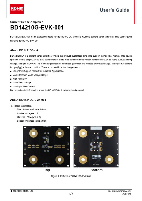
Current Sense AmplifierBD14210G-EVK-001BD14210G-EVK-001 is an evaluation board for BD14210G-LA, which is ROHM’s current sense amplifier. This user’s guide explains BD14210G-EVK-001.About BD14210G-LABD14210G-LA is a current sense amplifier. This is the product guarantees long time support in Industrial market. This device operates from a single 2.7V to 5.5V power supply. It has wide common mode voltage range from -0.2V to +26V, outputs analog voltage. The gain is 20 V/V. The matched gain resistor minimizes gain error and realizes low offset voltage. The input bias current is 1 μA (Typ) at typical condition. There is no need to adjust the gain error.■Long Time Support Product for Industrial Applications■Wide Common Mode Voltage Range■High Accuracy■Low Offset Voltage■Low Input Bias CurrentFor more detailed information about the BD14210G-LA, refer to the datasheet.About BD14210G-EVK-0011.Board Information・Size:90mm x 80mm x 1.6mm・Number of Layers:2・Material:FR-4 (~125°C)・Copper Thickness:2oz (70μm)Figure 1. Pictures of BD14210G-EVK-0012.Schematic DiagramFigure 2. Schematic Diagram of BD14210G-EVK-0013.Bill of MaterialsTable 1. Bill of Materials of BD14210G-EVK-001Part Part Type Manufacturer Value Size/PackageDescription U1 BD14210G-LA ROHM Co., Ltd. - SSOP6 Current Sense Amplifier C1 GRM188B31H104KA92DMurata ManufacturingCo., Ltd.0.1uF 1608(0603) Capacitor C2, C3, C4 N.M.-- 1608(0603) Capacitor R1, R2 N.M.-- 1608(0603) Resistor R3, R4 MCR03EZPJ000ROHM Co., Ltd.0Ω 1608(0603) Resistor R5, R7 N.M.-- 5025(2010) Shunt Resistor R6 LTR50UZPFU10L0ROHM Co., Ltd.10mΩ 5025(2010) Shunt Resistor D1, D2 N.M. -- DO-214AA (SMB) /SOD-323FLZener Diode CN1PH-1x5SGUseconn ElectronicsLtd.-1x5 pinConnectorNote: Only the materials used in BD14210G-EVK-001 are listed. N.M. = Not Mounted4.Layout(Top View)Figure 3. Layouts of BD14210G-EVK-0015.Reference Application DataFigure 4. Thermal simulation resultNote: These data are reference using a thermal simulation tool. Please note that the temperature will change depending on the actual usage environment.Please use this board under the condition that the heat generated by the shunt resistor does not exceed the usable temperature of the board, 125°C.The current values listed are reference, so when changing the current value, please use this board within the rated power of the shunt resistor.NoticeROHM Customer Support System/contact/Thank you for your accessing to ROHM product informations.More detail product informations and catalogs are available, please contact us.N o t e sThe information contained herein is subject to change without notice.Before you use our Products, please contact our sales representative and verify the latest specifica-tions :Although ROHM is continuously working to improve product reliability and quality, semicon-ductors can break down and malfunction due to various factors.Therefore, in order to prevent personal injury or fire arising from failure, please take safety measures such as complying with the derating characteristics, implementing redundant and fire prevention designs, and utilizing backups and fail-safe procedures. ROHM shall have no responsibility for any damages arising out of the use of our Poducts beyond the rating specified by ROHM.Examples of application circuits, circuit constants and any other information contained herein areprovided only to illustrate the standard usage and operations of the Products. The peripheral conditions must be taken into account when designing circuits for mass production.The technical information specified herein is intended only to show the typical functions of andexamples of application circuits for the Products. ROHM does not grant you, explicitly or implicitly, any license to use or exercise intellectual property or other rights held by ROHM or any other parties. ROHM shall have no responsibility whatsoever for any dispute arising out of the use of such technical information.The Products specified in this document are not designed to be radiation tolerant.For use of our Products in applications requiring a high degree of reliability (as exemplifiedbelow), please contact and consult with a ROHM representative : transportation equipment (i.e. cars, ships, trains), primary communication equipment, traffic lights, fire/crime prevention, safety equipment, medical systems, servers, solar cells, and power transmission systems.Do not use our Products in applications requiring extremely high reliability, such as aerospaceequipment, nuclear power control systems, and submarine repeaters.ROHM shall have no responsibility for any damages or injury arising from non-compliance withthe recommended usage conditions and specifications contained herein.ROHM has used reasonable care to ensur e the accuracy of the information contained in thisdocument. However, ROHM does not warrants that such information is error-free, and ROHM shall have no responsibility for any damages arising from any inaccuracy or misprint of such information.Please use the Products in accordance with any applicable environmental laws and regulations,such as the RoHS Directive. For more details, including RoHS compatibility, please contact a ROHM sales office. ROHM shall have no responsibility for any damages or losses resulting non-compliance with any applicable laws or regulations.W hen providing our Products and technologies contained in this document to other countries,you must abide by the procedures and provisions stipulated in all applicable export laws and regulations, including without limitation the US Export Administration Regulations and the Foreign Exchange and Foreign Trade Act.This document, in part or in whole, may not be reprinted or reproduced without prior consent ofROHM.1) 2)3)4)5)6)7)8)9)10)11)12)13)。
MGate 5114设备说明书

P/N: 1802051140010 *1802051140010*MGate 5114Quick Installation GuideEdition 1.0, November 2018Technical Support Contact Information/supportMoxa Americas:Toll-free: 1-888-669-2872 Tel: 1-714-528-6777 Fax: 1-714-528-6778 Moxa China (Shanghai office): Toll-free: 800-820-5036 Tel: +86-21-5258-9955 Fax: +86-21-5258-5505 Moxa Europe:Tel: +49-89-3 70 03 99-0 Fax: +49-89-3 70 03 99-99 Moxa Asia-Pacific:Tel: +886-2-8919-1230 Fax: +886-2-8919-1231 Moxa India:Tel: +91-80-4172-9088 Fax: +91-80-4132-10452018 Moxa Inc. All rights reserved.OverviewThe MGate 5114 is an industrial Ethernet gateway for ModbusRTU/ASCII/TCP and IEC 60870-5-101/104 network communications. Package ChecklistBefore installing the MGate 5114, verify that the package contains the following items:• 1 MGate 5114 gateway• 1 serial cable: DBL-RJ45F9-150•Quick installation guide (printed)•Warranty cardPlease notify your sales representative if any of the above items is missing or damaged.Optional Accessories (can be purchased separately)•CBL-F9M9-150: DB9-female-to-DB9-male serial cable, 150 cm •CBL-F9M9-20: DB9-female-to-DB9-male serial cable, 20 cm •CBL-RJ45F9-150: RJ45-to-DB9-female serial cable, 150 cm •CBL-RJ45SF9-150: RJ45-to-DB9-female serial shielded cable, 150 cm•Mini DB9F-to-TB DB9: Female-to-terminal-block connector •DK-25-01: 1 DIN-rail kit with 2 screws•WK-36-02: Wall-mounting kit, 2 plates with 6 screws•CBL-PJTB-10: Non-locking barrel plug to bare-wire cable Hardware IntroductionLED IndicatorsAgent Mode:LED Color DescriptionReady Off Power is off or a fault condition existsGreen Steady: Power is on, and the MGate isfunctioning normallyRed Steady: Power is on, and the MGate is bootingupBlinking slowly: Indicates an IP conflict, or theDHCP or BOOTP server is not respondingproperlyFlashing quickly: the microSD card failedMB* Off No serial communication with Modbus device Green Normal Modbus serial communication inprogressRed An error in serial communication occurredWhen the MGate 5114 acts as a ModbusRTU/ASCII master:1.The slave device returned an error(exception)2.Received a framing error (parity error,checksum error)3.Timeout (the master sends but noresponse)When the MGate 5114 acts as a ModbusRTU/ASCII slave:1.Received an invalid function codeThe master accessed an invalid registeraddress or coil address2.Received a framing error (parity error,checksum error)101* Off No serial communication with the IEC 60870-5-101 deviceGreen Normal IEC 60870-5-101 serial communicationin progressRed An error in serial communication occurredWhen the MGate 5114 acts as an IEC 60870-5-101 master:1.Received a slave exception (format error,checksum error, invalid data, slaveresponds are not supported)2.Timeout (the master sends but noresponse)When the MGate 5114 acts as an IEC 60870-5-101 slave:Received a master exception (format error,checksum error, invalid data)*Only indicates serial communication status; for IEC 60870-5-104 or Modbus TCP status, please refer to the LED indicator on the Ethernet port.DimensionsUnit: mm (inch)Reset ButtonRestore the MGate to factory default settings by using a pointed object (such as a straightened paper clip) to hold the reset button down until the Ready LED stops blinking (approximately five seconds).Pull-high, Pull-low, and Terminator for RS-485Beneath the MGate 5114’s top cover, you will find DIP switches to adjust each serial port’s pull-high resistor, pull-low resistor, and terminator.SW 1 2 3 Pull-high resistor Pull-low resistor Terminator ON1 kΩ 1 k Ω 120 Ω OFF 150 k Ω*150 k Ω*–**DefaultHardware Installation Procedure1. Connect the power adapter. Connect the 12-48 VDC power line orDIN-rail power supply to the MGate 5114’s terminal block.2. Use a serial cable to connect the MGate to the Modbus RTU/ASCIIor IEC 60870-5-101 device.3. Use an Ethernet cable to connect the MGate to the Modbus TCP orIEC 60870-5-104 device.4. The MGate 5114 is designed to be attached to a DIN rail ormounted on a wall. For DIN-rail mounting, push down the spring and properly attach it to the DIN rail until it “snaps” into place. For wall mounting, install the wall-mount kit (optional) first and then screw the device onto the wall.The following figure illustrates the two mounting options:Software Installation InformationYou can download the User's Manual and Device Search Utility (DSU) from Moxa's website: . Please refer to the User’s Manual for additional details on using the DSU.The MGate 5114 also supports login via a web browser. Default IP address: 192.168.127.254 Default account: admin Default password: moxaPin AssignmentsSerial Port (Male DB9) PinRS-232RS-422/ RS-485 (4W)RS-485 (2W) 1 DCD TxD-(A) – 2 RXD TxD+(B) –3 TXD RxD+(B)Data+(B) 4 DTR RxD-(A) Data-(A) 5* GND GND GND 6 DSR – – 7 RTS – – 8 CTS – – 9 – ––*Signal groundEthernet Port (RJ45) Pin Signal 1 Tx+ 2 Tx- 3 Rx+ 6Rx-Power Input and Relay Output PinoutsV2+V2-V1+V1-ShieldedGroundDC Power Input 2 DCPowerInput 2 N.O.CommonN.C.DC Power Input 1 DC Power Input 1SpecificationsPower Requirements Power Input 12 to 48 VDC Input Current455 mA max.Operating TemperatureStandard models:0 to 60°C (32 to 140°F) Wide temp. models:-40 to 75°C (-40 to 167°F)Ambient Relative Humidity 5 to 95% (non-condensing) Dimensions 36 x 105 x 140 mm (1.42 x 4.14 x 5.51 in) Reliability Alert Tools Built-in buzzer and RTC MTBF 1,140,815 hrs.。
MC1GU064HDCA-0QC00中文资料

MultiMediaCard SpecificationVersion : Ver. 0.9Date 4 – June - 2004Samsung Electronics Co., LTDSemiconductor Flash Memory Product Planning & Applications1 Introduction to the MultiMediaCard ----------------------------------------------------------- 51.1 System Features ----------------------------------------------------------------------------------------- 5-------------------------------------------------------------------------------------- 51.2 ProductModel2 Function Description ------------------------------------------------------------------------------- 72.1 Flash Technology Independence ------------------------------------------------------------------ 72.2 Defect and Error Management --------------------------------------------------------------------- 72.3 Endurance ----------------------------------------------------------------------------------------------- 72.4 Automatic Sleep Mode ------------------------------------------------------------------------------- 72.5 Hot Insertion -------------------------------------------------------------------------------------------- 82.6 MultiMediaCard Mode -------------------------------------------------------------------------------- 82.6.1 MultiMediaCard Standard Compliance ----------------------------------------------------------- 82.6.2 Negotiation Operation Conditions ----------------------------------------------------------------- 82.6.3 Card Acquisition and Identification ---------------------------------------------------------------- 82.6.4 Card Status ---------------------------------------------------------------------------------------------- 82.6.5 Memory Array Partitioning --------------------------------------------------------------------------- 92.6.6 Read and Write Operations ------------------------------------------------------------------------- 92.6.7 Data Transfer Rate ------------------------------------------------------------------------------------102.6.8 Data Protection in the Flash Card -----------------------------------------------------------------10-----------------------------------------------------------------------------------------------------10 2.6.9 Erase2.6.10 Write Protection ----------------------------------------------------------------------------------------102.6.11 Copy Bit ------------------------------------------------------------------------------------------------- 102.6.12 The CSD Register ------------------------------------------------------------------------------------ 112.7 SPI Mode ----------------------------------------------------------------------------------------------- 112.7.1 Negotiating Operation Conditions ---------------------------------------------------------------- 112.7.2 Card Acquisition and Identification --------------------------------------------------------------- 112.7.3 Card Status --------------------------------------------------------------------------------------------- 112.7.4 Memory Array Partitioning -------------------------------------------------------------------------- 112.7.5 Read and Write Operations ------------------------------------------------------------------------- 112.7.6 Data Transfer Rate ------------------------------------------------------------------------------------ 112.7.7 Data Protection in the MultiMediaCard ----------------------------------------------------------- 1212-----------------------------------------------------------------------------------------------------2.7.8 Erase2.7.9 Write Protection ---------------------------------------------------------------------------------------- 123 Product Specifications ----------------------------------------------------------------------------- 133.1 Recommended Operating Conditions ------------------------------------------------------------------------- 133.2 Operating Characteristis ----------------------------------------------------------------- 143.3 System Environmental Specifications ----------------------------------------------------------------- 153.4 System Reliability and Maintenance -------------------------------------------------------------- 153.5 Physical Specifications ------------------------------------------------------------------------------- 164 MultiMediaCard Interface Description --------------------------------------------------------- 174.1 Pin Assignments in MultiMediaCard Mode ------------------------------------------------------- 174.2 Pin Assignments in SPI Mode ---------------------------------------------------------------------- 184.3 MultiMediaCard Bus Topology ---------------------------------------------------------------------- 184.4 SPI Bus Topology -------------------------------------------------------------------------------------------------- 194.4.1 SPI Interface Concept ------------------------------------------------------------------------------------------- 194.4.2 SPI Bus Topology ------------------------------------------------------------------------------------------------ 1920------------------------------------------------------------------------------------------------- 4.5 Registers4.5.1 Operation Condition Register (OCR) ---------------------------------------------------------------------------204.5.2 Card Identification (CID) ------------------------------------------------------------------------------214.5.3 Relative Card Address (RCA) ----------------------------------------------------------------------- 21 4.5.4 Card Specific Data (CSD) ---------------------------------------------------------------------------- 22 4.6 MultiMediaCard Communication -------------------------------------------------------------------- 3030----------------------------------------------------------------------------------------------- 4.6.1 Commands4.7 Read, Write and Erase Time-out Conditions ----------------------------------------------------- 33 4.8 Card Identification Mode ------------------------------------------------------------------------------ 34 4.8.1 Operating Voltage Range Validation --------------------------------------------------------------- 35 4.9 Data Transfer Mode ------------------------------------------------------------------------------------ 35 4.9.1 Block Read ----------------------------------------------------------------------------------------------- 37 4.9.2 Block Write ----------------------------------------------------------------------------------------------- 3738------------------------------------------------------------------------------------------------------ 4.9.3 Erase4.9.4 Write Protect Management -------------------------------------------------------------------------- 38 4.9.5 Card Lock/Unlock Operation ------------------------------------------------------------------------ 38----------------------------------------------------------------------------------------------- 41 4.9.6 Responses4.9.7 Status ------------------------------------------------------------------------------------------------------ 42 4.9.8 Command Response Timing ------------------------------------------------------------------------ 4448 4.9.9 Reset------------------------------------------------------------------------------------------------------ 4.10 SPI Communication ----------------------------------------------------------------------------------- 49 4.10.1 Mode Selection ----------------------------------------------------------------------------------------- 49 4.10.2 Bus Transfer Protection ------------------------------------------------------------------------------ 49 4.10.3 Data Read Overview ---------------------------------------------------------------------------------- 50 4.10.4 Data Write Overview ---------------------------------------------------------------------------------- 51 4.10.5 Erase and Write Protect Management ----------------------------------------------------------- 52 4.10.6 Reading CID/CSD Registers ------------------------------------------------------------------------ 53 4.10.7 Reset Sequence --------------------------------------------------------------------------------------- 53 4.10.8 Error Conditions ---------------------------------------------------------------------------------------- 53 4.10.9 Memory Array Partitioning --------------------------------------------------------------------------- 53 4.10.10 Card Lock/Unlock -------------------------------------------------------------------------------------- 53 4.10.11 Commands ----------------------------------------------------------------------------------------------- 54 4.10.12 Responses ----------------------------------------------------------------------------------------------- 56 4.10.13 Data Tokens --------------------------------------------------------------------------------------------- 58 4.10.14 Data Error Token --------------------------------------------------------------------------------------- 59 4.10.15 Clearing Status Bits ------------------------------------------------------------------------------------ 60 4.11 SPI Bus Timing ----------------------------------------------------------------------------------------- 61 4.12 Error Handling ------------------------------------------------------------------------------------------ 64 4.12.1 Error Correction Code (ECC) ----------------------------------------------------------------------- 64 4.12.2 Cyclic Redundancy Check (CRC) ----------------------------------------------------------------- 642 Function Description2.1 Flash Technology IndependenceThe 512 byte sector size of the MultiMediaCard is the same as that in an IDE magnetic disk drive. To write or read a sector (or multiple sectors), the host computer software simply issues a Read or Write command to the MultiMediaCard. This command contains the address and the number of sectors to write/read. The host software then waits for the command to complete. The host software does not get involved in the details of how the flash memory is erased, programmed or read. This is extremely important as flash devices are expected to get more and more complex in the future. Because the MultiMediaCard uses an intelligent on-board controller, the host system software will not require changing as new flash memory evolves. In other words, systems that support the MultiMediaCard today will be able to access future MultiMediaCards built with new flash technology without having to update or change host software.2.2 Defect and Error ManagementMultiMediaCards contain a sophisticated defect and error management system. This system is analogous to the systems found in magnetic disk drives and in many cases offers enhancements. For instance, disk drives do not typically perform a read after write to confirm the data is written correctly because of the performance penalty that would be incurred. MultiMediaCards do a read after write under margin conditions to verify that the data is written correctly (except in the case of a Write without Erase Command). In the rare case that a bit is found to be defective, MultiMediaCards replace this bad bit with a spare bit within the sector header. If necessary, MultiMediaCards will even replace the entire sector with a spare sector. This is completely transparent to the host and does not consume any user data space.The MultiMediaCards soft error rate specification is much better than the magnetic disk drive specification. In the extremely rare case a read error does occur, MultiMediaCards have innovative algorithms to recover the data. This is similar to using retries on a disk drive but is much more sophisticated. The last line of defense is to employ powerful ECC to correct the data. If ECC is used to recover data, defective bits are replaced with spare bits to ensure they do not cause any future problems.These defect and error management systems coupled with the solid-state construction give MultiMediaCards unparalleled reliability2.3 EnduranceMultiMediaCards have an endurance specification for each sector of 1,000,000 writes (reading a logical sector is unlimited). This is far beyond what is needed in nearly all applications of MultiMediaCards. Even very heavy use of the MultiMediaCard in cellular phones, personal communicators, pagers and voice recorders will use only a fraction of the total endurance over the typical device’s five year lifetime. For instance, it would take over 100 years to wear out an area on the MultiMediaCard on which a files of any size (from 512 bytes to capacity) was rewritten 3 times per hour, 8 hours a day, 365 days per year.With typical applications the endurance limit is not of any practical concern to the vast majority of users.2.4 Automatic Sleep ModeAn important feature of the MultiMediaCard is automatic entrance and exit from sleep mode. Upon completion of an operation, the MultiMediaCard will enter the sleep mode to conserve power if no further commands are received within 5 msec The host does not have to take any action for this to occur. In most systems, the MultiMediaCard is in sleep mode except when the host is accessing it, thus conserving power. When the host is ready to access the MultiMediaCard and it is in sleep mode, any command issued to the MultiMediaCard will cause it to exit sleep and respond. The host does not have to issue a reset first. It may do this if desired, but it is not needed. By not issuing the reset, performance is improved through the reduction of overhead.2.5 Hot InsertionSupport for hot insertion will be required on the host but will be supported through the connector. Connector manufacturers will provide connectors that have power pins long enough to be powered before contact is made with the other pins. Please see connector data sheets for more details. This approach is similar to that used in PCMCIA to allow for hot insertion. This applies to both MultiMediaCard and SPI modes.2.6 MultiMediaCard Mode2.6.1 MultiMediaCard Standard ComplianceThe MultiMediaCard is fully compliant with MultiMediaCard standard specification V3.31.The structure of the Card Specific Data (CSD) register is compliant with CSD structure V1.2.2.6.2 Negotiating Operation ConditionsThe MultiMediaCard supports the operation condition verification sequence defined in the MultiMediaCard standard specifications. The MultiMediaCard host should define an operating voltage range that is not supported by the MultiMediaCard. It will put itself in an inactive state and ignore any bus communication. The only way to get the card out of the inactive state is by powering it down and up again. In addition the host can explicitly send the card to the inactive state by using the GO_INACTIVE_STATE command.2.6.3 Card Acquisition and IdentificationThe MultiMediaCard bus is a single master (MultiMediaCard host) and multi-slaves (cards) bus. The host can query the bus and find out how many cards of which type are currently connected. The MultiMediaCard’s CID register is pre-programmed with a unique card identification number which is used during the acquisition and identification procedureIn addition, the MultiMediaCard host can read the card’s CID register using the READ_CID MultiMediaCard command. The CID register is programmed during the MultiMediaCard testing and formatting procedure, on the manufacturing floor. The MultiMediaCard host can only read this register and not write to it.2.6.4 Card StatusMultiMediaCard status is stored in a 32 bit status register which is sent as the data field in the card respond to host commands. Status register provides information about the card’s current state and completion codes for the last host command. The card status can be explicitly read (polled) with the SEND_STATUS command.2.6.7 Data Protection in the Flash CardEvery sector is protected with an Error Correction Code (ECC). The ECC is generated (in the memory card) when the sectors are written and validated when the data is read. If defects are found, the data is corrected prior to transmission to the host.The MultiMediaCard can be considered error free and no additional data protection is needed. However, if an application uses additional, external, ECC protection, the data organization is defined in the user writeable section of the CSD register2.6.8 EraseThe smallest erasable unit in the MultiMediaCard is a erase group. In order to speed up the erase procedure, multiple erase groups can be erased in the same time. The erase operation is divided into two stages.Tagging - Selecting the Sectors for ErasingTo facilitate selection, a first command with the starting address is followed by a second command with the final address, and all erase groups within this range will be selected for erase.Erasing - Starting the Erase ProcessTagging can address erase groups. An arbitrary selection of erase groups may be erased at one time. Tagging and erasing must follow a strict command sequence (refer to the MultiMediaCard standard specification for details).2.6.9 Write ProtectionThe MultiMediaCard erase groups are grouped into write protection groups. Commands are provided for limiting and enabling write and erase privileges for each group individually. The current write protect map can be read using SEND_WRITE_PROT command.In addition two, permanent and temporary, card levels write protection options are available.Both can be set using the PROGRAM_CSD command (see below). The permanent write protect bit, once set, cannot be cleared.The One Time Programmable (OTP) characteristic of the permanent write protect bit is implemented in the MultiMediaCard controller firmware and not with a physical OTP cell.2.6.10 Copy BitThe content of an MultiMediaCard can be marked as an original or a copy using the copy bit in the CSD register. Once the Copy bit is set (marked as a copy) it cannot be cleared.The Copy bit of the MultiMediaCard is programmed (during test and formatting on the manufacturing floor) as a copy. The MultiMediaCard can be purchased with the copy bit set (copy) or cleared, indicating the card is a master.The One Time Programmable (OTP) characteristic of the Copy bit is implemented in the MultiMediaCard controller firmware and not with a physical OTP cell.2.6.11 The CSD RegisterAll the configuration information of the MultiMediaCard is stored in the CSD register. The MSB bytes of the register contain manufacturer data and the two least significant bytes contains the host controlled data - the card Copy and write protection and the user ECC register.The host can read the CSD register and alter the host controlled data bytes using the SEND_CSD and PROGRAM_CSD commands.2.7 SPI ModeThe SPI mode is a secondary (optional) communication protocol offered for MultiMediaCard. This mode is a subset of the MultiMediaCard protocol, designed to communicate with an SPI channel, commonly found in Motorola’s (and lately a few other vendors’) microcontrollers.2.7.1 Negotiating Operation ConditionsThe operating condition negotiation function of the MultiMediaCard bus is not supported in SPI mode. The host must work within the valid voltage range (2.7 to 3.6 volts) of the card.2.7.2 Card Acquisition and IdentificationThe card acquisition and identification function of the MultiMediaCard bus is not supported in SPI mode. The host must know the number of cards currently connected on the bus. Specific card selection is done via the CS signal.2.7.3 Card StatusIn SPI mode only 16 bits (containing the errors relevant to SPI mode) can be read out of the MultiMediaCard status register.2.7.4 Memory Array PartitioningMemory partitioning in SPI mode is equivalent to MultiMediaCard mode. All read and write commands are byte addressable.2.7.5 Read and Write OperationsIn SPI mode, only single block read/write mode is supported.2.7.6 Data Transfer RateIn SPI mode only block mode is supported. The typical access time (latency) for each data block, in read operation, is 1.5mS. The write typical access time (latency) for each data block, in read operation, is 1.5mS. The write block operation is done in handshake mode. The card will keep DataOut line low as long as the write operation is in progress and there are no write buffers available.2.7.7 Data Protection in the MultiMediaCardSame as for the MultiMediaCard mode.2.7.8 EraseSame as in MultiMediaCard mode2.7.9 Write ProtectionSame as in MultiMediaCard modeFigure 3-1 Timing Diagram of Data Input and Output3.5 Physical SpecificationsDimensions of Normal MMC(24mm x 32mm x 1.4mm)Dimensions of RS-MMC(24mm x 18mm x 1.4mm)rising and falling edges). If the host does not allow the switchable R OD implementation, a fix R CMD can be used. Consequently the maximum operating implementation, a fix R CMD can be used. Consequently the maximum operating frequency in the open drain mode has to be reduced in this case.4.4 SPI Bus Topology4.4.1 SPI Interface ConceptThe Serial Peripheral Interface (SPI) is a general-purpose synchronous serial interface originally found on certain Motorola micro-controllers. The MultiMediaCard SPI interface is compatible with SPI hosts available on the market. As any other SPI device the MultiMediaCard SPI channel consists of the following 4 signals:- CS : Host to card chip select signal- CLK : Host to card clock signal- DataIn : Host to card data signal- DataOut : Card to host data signalAnother SPI common characteristic, which is implemented in the MultiMediaCard card as well, is byte transfers. All data tokens are multiples of 8 bit bytes and always byte aligned to the CS signal. The SPI standard defines the physical link only and not the complete data transfer protocol. The MultiMediaCard uses a subset of the MultiMediaCard protocol and command set.4.4.2 SPI Bus TopologyThe MultiMediaCard card identification and addressing algorithms are replaced by hardware Chip Select (CS) signal. There are no broadcast commands. A card (slave) is selected, for every command, by asserting (active low) the CS signal (see Figure 4-3). The CS signal bust is continuously active for the duration of the SPI transaction (command, response and data). The only exception is card-programming time. At this time the host can de-assert the CS signal without affecting the programming process. The bi-directional CMD and DAT lines are replaced by unidirectional dataIn and dataOut signals. This eliminates the ability of executing commands while data is being read or written and, therefore, eliminates the sequential and multi block read/write operations. The SPI channel supports only single block read/write.Figure 4-3 SPI Bus SystemReadThe read access time is defined as the sum of the two times given by the CSD parameters TAAC and NSAC (refer to Table “Card Specific Data (CSD)”). These card parameters define the typical delay between the end bit of the read command and the start bit of the data block. This number is card dependent and should be used by the host to calculate throughput and the maximal frequency for stream read.WriteThe R2W_FACTOR field in the CSD is used to calculate the typical block program time obtained by multiplying the read access time by this factor. It applies to all write/erase commands (e.g. SET(CLEAR)_WRITE_PROTECT, PROGRAM_CSD(CID) and the block write commands). It should be used by the host to calculate throughput.EraseThe duration of an erase command will be (order of magnitude) the number of sectors to be erased multiplied by the block write delay.4.8 Card Identification ModeAll the data communication in the card identification mode uses only the command line (CMD). MultiMediaCard State Diagram (Card Identification Mode)Figure 4-2 MultiMediaCard State Diagram (Card Identification Mode)The host starts the card identification process in open drain mode with the identification clock rate f OD(generated by a push pull driver stage). The open drain driver stages on the CMD line allow the parallel card operation during card identification. After the bus is activated the host will request the cards to send their valid operation conditions with the command SEND_OP_COND (CMD1). Since the bus is in open drain mode, as long as there is more than one card with operating conditions restrictions, the host gets in the response to the CMD1 a “wired or” operation condition restrictions of those cards. The host then must pick a common denominator for operation and notify the application that cards with out of range parameters (from the host perspective) are connected to the bus. Incompatible cards go into Inactive State (refer to also Chapter “Operating Voltage Range Validation”). The busy bit in the CMD1 response can be used by a card to tell the host that it is still working on its power-up/reset procedure (e.g. downloading the register information from memory field) and is not ready yet for communication. In this case the host must repeat CMD1 until the busy bit is cleared. After an operating mode is established, the host asks all cards for their unique card identification (CID) number with the broadcast command ALL_SEND_CID (CMD2).All not already identified cards (i.e. those which are in Ready State) simultaneously start sending their CID numbers serially, while bit-wise monitoring their outgoing bitstream. Those cards, whose outgoing CID bits do not match the corresponding bits on the command line in any one of the bit periods, stop sending their CID immediately and must wait for the next identification cycle (cards stay in the Ready State). There should be only one card which successfully sends its full CID-number to the host. This card then goes into the Identification State. The host assigns to this card (using CMD3, SET_RELATIVE_ADDR) a relative card address (RCA, shorter than CID), which will be used to address the card in future communication (faster than with the CID). Once the RCA is received the card transfers to the Standby State and does not react to further identification cycles. The card also switches the output drivers from the open-drain to the push-pull mode in this state. The host repeats the identification process as long as it receives a response (CID) to its identification command (CMD2). When no card responds to this command, all cards have been identified. The time-out condition to recognize this, is waiting for the start bit for more than 5 clock periods after sending CMD24.8.1 Operating Voltage Range ValidationThe MultiMediaCard standards operating range validation is intended to support reduced voltage range MultiMediaCards. The MultiMediaCard supports the range of 2.7 V to 3.6V supply voltage. So the MultiMediaCard sends a R3 response to CMD1 which contains an OCR value of 0x80FF8000 if the busy flag is set to “ready” or 0x00FF8000 if the busy flag is active (refer to Chapter “Responses”). By omitting the voltage range in the command, the host can query the card stack and determine the common voltage range before sending out-of-range cards into the Inactive State. This bus query should be used if the host is able to select a common voltage range or if a notification to the application of non usable cards in the stack is desired. Afterwards, the host must choose a voltage for operation and reissue CMD1 with this condition sending incompatible cards into the Inactive State.4.9 Data Transfer ModeWhen in Standby State, both CMD and DAT lines are in the push-pull mode. As long as the content of all CSD registers is not known, the f PushPull clock rate is equal to the slow f OpenDrain clock rate. SEND_CSD (CMD9) allows the host to get the Card Specific Data (CSD register), e.g. ECC type, block length, card storage capacity, maximum clock rate etc..。
Moxa ioLogik R1200 Series RS-485远程I O产品说明书

ioLogik R1200SeriesRS-485remote I/OFeatures and Benefits•Dual RS-485remote I/O with built-in repeater•Supports the installation of multidrop communications parameters•Install communications parameters and upgrade firmware via USB•Upgrade firmware through an RS-485connection•Wide operating temperature models available for-40to85°C(-40to185°F)environmentsCertificationsIntroductionThe ioLogik R1200Series RS-485serial remote I/O devices are perfect for establishing a cost-effective,dependable,and easy-to-maintain remote process control I/O system.Remote serial I/O products offer process engineers the benefit of simple wiring,as they only require two wires to communicate with the controller and other RS-485devices while adopting the EIA/TIA RS-485communication protocol to transmit and receive data at high speed over long distances.In addition to communication configuration by software or USB and dual RS-485port design,Moxa’s remote I/O devices eliminate the nightmare of extensive labor associated with the setup and maintenance of data acquisition and automation systems.Moxa also offers different I/O combinations,which provide greater flexibility and are compatible with many different applications.Easy-to-Use Software Interface for Easy MaintenanceWith Moxa’s easy-to-use ioSearch software,you can quickly access all of an ioLogik R1200device’s status information and settings with a user-friendly graphical user interface.Furthermore,ioSearch also provides an easy method for updating firmware for all ioLogik R1200devices over an RS-485network,so you can even update your firmware remotely.The free and easy-to-use ioSearch software reduces the maintenance time and labor required to set up your communication interface.When more than one ioLogik R1200are on the same RS-485network,you no longer need to turn hundreds of dials during setup.Instead,simply configure and duplicate each ioLogik R1200’s baudrate and mode through the graphical user interface.This convenient software feature reduces maintenance engineers'effort,and greatly simplifies upgrading your device's configuration compared with more traditional methods.Innovative Hardware Design Reduces Deployment Effort and Enhances Maintenance EfficiencyWith the industry’s first RS-485serial remote I/O with USB design,Moxa provides an innovative solution for upgrading and configuring RS-485 remote I/O communication devices and firmware.All you need to do is upload the configurations to a USB drive,plug it into the field device,and all the configurations and firmware updates will upload to the field device automatically.Cost-Saving Hardware Design for Backup and RedundancyMoxa’s ioLogik R1200Series provides dual RS-485ports so that when one of your RS-485ports is damaged,you can quickly switch to the other RS-485port for quick testing or repair.RS-485remote I/O devices are already considered a low-cost technology,but with dual RS-485ports,Moxa helps you save a little bit more.With the ioLogik R1200,you can take advantage of our dual RS-485ports to set up wiring,provide computer redundancy,or back up your network using two computer topologies.For wiring redundancy,when your computer detects that one of the RS-485 connections is not responding,it can quickly switch over to the other RS-485line to guarantee continuous communication between field sensors and the central computer.Furthermore,users have the freedom to define the settings.For computer redundancy,the ioLogik R1200provides system operators with a secure backup when one system goes down.SpecificationsInput/Output InterfaceButtons Reset buttonAnalog Input Channels ioLogik R1240Series:8Analog Output Channels ioLogik R1241Series:4Configurable DIO Channels(by software)ioLogik R1212Series:8Digital Input Channels ioLogik R1210Series:16ioLogik R1212Series:8ioLogik R1214Series:6Isolation3k VDC or2k VrmsRelay Channels ioLogik R1214Series:6Digital InputsConnector Screw-fastened Euroblock terminal Counter Frequency 2.5kHzDigital Filtering Time Interval Software configurableDry Contact On:short to GNDOff:openI/O Mode DI or event counterPoints per COM ioLogik R1210/R1212Series:8channelsioLogik R1214Series:6channels Sensor Type Dry contactWet Contact(NPN or PNP)Wet Contact(DI to COM)On:10to30VDCOff:0to3VDCDigital OutputsConnector Screw-fastened Euroblock terminalCurrent Rating200mA per channelI/O Mode DO or pulse outputI/O Type SinkOver-Current Protection0.65A per channel@25°COver-Temperature Shutdown175°C(typical),150°C(min.)Over-Voltage Protection35VDCPulse Output Frequency5kHzRelaysBreakdown Voltage500VACConnector Screw-fastened Euroblock terminalContact Current Rating Resistive load:5A@30VDC,250VAC,110VACContact Resistance100milli-ohms(max.)Electrical Endurance100,000operations@5A resistive loadInitial Insulation Resistance1,000mega-ohms(min.)@500VDCMechanical Endurance5,000,000operationsPulse Output Frequency0.3Hz at rated loadType Form A(N.O.)power relayNote Ambient humidity must be non-condensing and remain between5and95%.The relaysmay malfunction when operating in high condensation environments below0°C. Analog InputsAccuracy ioLogik R1240:±0.1%FSR@25°C±0.3%FSR@-10to60°CioLogik R1240-T:±0.1%FSR@25°C±0.3%FSR@-10to60°C±0.5%FSR@-40to75°CBuilt-in Resistor for Current Input120ohmsConnector Screw-fastened Euroblock terminalI/O Mode Voltage/CurrentI/O Type DifferentialInput Impedance10mega-ohms(min.)Input Range0to10VDC0to20mA4to20mA4to20mA(with burn-out detection)Resolution16bitsSampling Rate All channels:12samples/secPer channel:1.5samples/secOnly one channel enabled:12samples/secAnalog OutputsAccuracy ioLogik R1241:±0.1%FSR@25°C±0.3%FSR@-10to60°CioLogik R1241-T:±0.1%FSR@25°C±0.3%FSR@-40to75°CConnector Screw-fastened Euroblock terminalLoad Resistor Internal register,400ohmsNote:24V of external power required when loading exceeds1,000ohms Output Range0to10VDC0to20mA4to20mAResolution12-bitVoltage Output10mA(max.)LED InterfaceLED Indicators PWR,RDY,P1,P2Serial InterfaceBaudrate1200bps to921.6kbpsConnector Terminal blockNo.of Ports2Parity None,Even,OddPull High/Low Resistor for RS-4851kilo-ohm,150kilo-ohmsSerial Standards RS-485Stop Bits1,2Surge1kVESD15kVData Bits8Serial SignalsRS-485-2w Data+,Data-,GNDSerial Software FeaturesIndustrial Protocols Modbus RTU Server(slave)Power ParametersPower Connector Screw-fastened Euroblock terminalNo.of Power Inputs1Input Voltage12to48VDCPower Consumption ioLogik R1210Series:154mA@24VDCioLogik R1212Series:187mA@24VDCioLogik R1214Series:207mA@24VDCioLogik R1240Series:216mA@24VDCioLogik R1241Series:343mA@24VDC Physical CharacteristicsHousing PlasticDimensions27.8x124x84mm(1.09x4.88x3.31in)Weight200g(0.44lb)Installation DIN-rail mounting,Wall mountingWiring I/O cable,16to26AWGPower cable,12to24AWGEnvironmental LimitsOperating Temperature Standard Models:-10to75°C(14to167°F)Wide Temp.Models:-40to85°C(-40to185°F) Storage Temperature(package included)-40to85°C(-40to185°F)Ambient Relative Humidity5to95%(non-condensing)Altitude2000m1Standards and CertificationsEMC EN55032/24EMI CISPR32,FCC Part15B Class AEMS IEC61000-4-2ESD:Contact:4kV;Air:8kVIEC61000-4-3RS:80MHz to1GHz:3V/mIEC61000-4-4EFT:Power:0.5kVIEC61000-4-5Surge:Power:2kVIEC61000-4-6CS:3VIEC61000-4-8PFMFSafety UL508Shock IEC60068-2-27Vibration IEC60068-2-6DeclarationGreen Product RoHS,CRoHS,WEEEMTBFTime1,239,293hrsStandards Telcordia SR332WarrantyWarranty Period ioLogik R1214:2years2ioLogik R1210/R1212/R1240/R1241Series:5years Details See /warranty1.Please contact Moxa if you require products guaranteed to function properly at higher altitudes.2.Because of the limited lifetime of power relays,products that use this component are covered by a2-year warranty.Package ContentsDevice1x ioLogik R1200Series remote I/OInstallation Kit1x terminal block,12-pin,3.81mm1x terminal block,3-pin,5.00mm1x terminal block,8-pin,3.81mmDocumentation1x quick installation guide1x warranty cardDimensionsOrdering InformationModel Name Input/Output Interface Operating Temp. ioLogik R121016x DI-10to75°C ioLogik R1210-T16x DI-40to85°C ioLogik R12128x DI,8x DIO-10to75°C ioLogik R1212-T8x DI,8x DIO-40to85°C ioLogik R12146x DI,6x Relay-10to75°C ioLogik R1214-T6x DI,6x Relay-40to85°C ioLogik R12408x AI-10to75°C ioLogik R1240-T8x AI-40to85°C ioLogik R12414x AO-10to75°C ioLogik R1241-T4x AO-40to85°CAccessories(sold separately)SoftwareMX-AOPC UA Server OPC UA Server software for converting fieldbus to the OPC UA standard©Moxa Inc.All rights reserved.Updated Nov12,2018.This document and any portion thereof may not be reproduced or used in any manner whatsoever without the express written permission of Moxa Inc.Product specifications subject to change without notice.Visit our website for the most up-to-date product information.。
RA参数表

11-4
Siemens Electrical Drives Ltd. 6RX1700-0AD50 SIMOREG DC Master 使用说明书
05.2007
参数号 说 明
值范围 [单位] 步长
11.1
r000
运行状态显示
运行状态显示 状态显示,故障和报警信息
(控制字 2,位 31,见 P691)
[自版本 1.8 起]
o4 等待电压(电枢)
o4.0 等待在电源端子 1U1,1V1,1W1 的电压。电压和频率必须在参数
P351,P352,P353,P363 和 P364 规定的范围内。也见 P078.001。
o4.1 等待熔断器监控器 OK 信号
[自版本 1.7 起]
o7 等待合闸指令( = READY TO SWITCH ON) o7.0 等待通过端子 37 的合闸指令。 o7.1 等待由开关量连接器(根据在参数 P654 中的选择)或控制字,0 位
(根据在参数 P648 中的选择)的合闸指令。 o7.2 等待通过一个外部分闸指令输入的内部分闸取消或等待“用励磁
功能 模拟量输出 开关量输出 基本整流器上串行接口的配置 监控功能的解除 补偿值 晶闸管诊断 关于 DriveMonitor 和 OP1S 的参数 程序文件参数 故障存贮器 只读参数: 报警 装置标志 只读参数: 控制字和状态字 复位和存储参数,现有的和更改的 P 和 r 参数 密码保护,钥匙/锁的作用原理 处理器利用率 其他 串行接口的开关量连接器/连接器的转换 换向监控 设定值的减小 输入和输出功能定义 继电器输出端子 109/110 功能意义 启动脉冲速度调节器 用于起重机 4 级主开关的计算 带有 SCI1 的 SCB1 的配置 在板安装位置 2 和 3 的附加板的配置 SIMOLINK 板的配置 EB1 扩展板的配置 EB2 扩展板的配置 SBP 脉冲编码器板的配置 并行接口的配置 用于 SIMOREG CM (控制模块)的参数 外部励磁单元额定直流电流 模拟工作模式 DriveMonitor 的参数 槽禁止激活 DriveMonitor 的参数 DriveMonitor 的参数 专家的参数存取 现存的和更改的 U 和 n 参数
欧诺克 直流无刷电机 产品说明书

深圳市欧诺克科技有限公司Shenzhen ONKE Technology Co., Ltd.座机:*************27381841电话:邓先生135****7106陈先生139****0920邮箱:***************网 址 : 地址:广东省深圳市宝安区福海街道怀德翠湖工业园13栋稳定的质量是我们赖以生存的根本优质的服务是我们继续发展的前提客户的满意是我们唯一追求的目标产品画册Product gallery专业生产伺服驱动器、伺服电机及自动化控制系统深圳市欧诺克科技有限公司直流无刷电机目录匠心制造精益求精“一、公司介绍01二、直流无刷电机021.电机介绍与型号说明032.电机应用领域043.电机规格参数表054.电机规格尺寸图06C O M P A N Y PROFILE以精密制造引领未来Leading the future with precision manufacturing公司简介Company Profile深圳市欧诺克科技有限公司成立于2010年,是一家专业研发生产伺服电机和驱动器的高新技术企业,公司技术力量雄厚,检测手段先进,欧诺克人本着不求最全,只求最精的信念,为生产出各类伺服电机、各类驱动器而不懈奋斗。
欧诺克人以鹰的精神,挑战尖端,研发生产出高性价比的各类伺服电机和驱动器,以鹰的敏锐洞察力洞察市场,与时俱进、创新来满足市场的需求。
深圳市欧诺克科技有限公司产品主要有:伺服驱动器、伺服电机、直流伺服驱动器,直流伺服电机,交流伺服驱动器,交流伺服电机,低压伺服驱动器,低压伺服电机,直线电机驱动器,DDR马达驱动器,音圈电机驱动器,直流无刷驱动器,直流无刷电机,CANopen总线、EtherCAT总线、电子凸轮伺服系统,大功率伺服驱动器、大电流伺服驱动器,专用运动控制伺服驱动器和自动化控制系统,十多年来凭借精湛的技术与国内国外众多知名企业公司建立了互利共赢的合作。
公司不断研究和开发满足行业需求的各类伺服电机和驱动器,帮助客户提升品质和生产效率。
LMC6041中文资料

LMC6041CMOS Single Micropower Operational AmplifierGeneral DescriptionUltra-low power consumption and low input-leakage current are the hallmarks of the LMC6041.Providing input currents of only 2fA typical,the LMC6041can operate from a single supply,has output swing extending to each supply rail,and an input voltage range that includes ground.The LMC6041is ideal for use in systems requiring ultra-low power consumption.In addition,the insensitivity to latch-up,high output drive,and output swing to ground without requir-ing external pull-down resistors make it ideal for single-supply battery-powered systems.Other applications for the LMC6041include bar code reader amplifiers,magnetic and electric field detectors,and hand-held electrometers.This device is built with National’s advanced Double-Poly Silicon-Gate CMOS process.See the LMC6042for a dual,and the LMC6044for a quad amplifier with these features.Featuresn Low supply current:14µA (Typ)n Operates from 4.5V to 15.5V single supply n Ultra low input current:2fA (Typ)n Rail-to-rail output swingnInput common-mode range includes groundApplicationsn Battery monitoring and power conditioning n Photodiode and infrared detector preamplifier n Silicon based transducer systems n Hand-held analytic instruments n pH probe buffer amplifiern Fire and smoke detection systemsnCharge amplifier for piezoelectric transducersConnection DiagramOrdering InformationTemperatureRangeNSC DrawingTransport MediaPackage Industrial −40˚C to +85˚C 8-Pin LMC6041AIM M08ARail Small Outline LMC6041IM Tape and Reel 8-Pin LMC6041AIN N08E RailMolded DIPLM6041IN8-Pin DIP/SODS011136-1December 1994LMC6041CMOS Single Micropower Operational Amplifier©1999National Semiconductor Corporation Absolute Maximum Ratings(Note1)If Military/Aerospace specified devices are required, please contact the National Semiconductor Sales Office/ Distributors for availability and specifications. Differential Input Voltage±Supply Voltage Supply Voltage(V+−V−)16V Output Short Circuit to V−(Note2) Output Short Circuit to V+(Note11) Lead Temperature(Soldering,10sec.)260˚C Storage Temperature Range−65˚C to+150˚C Junction Temperature110˚C ESD Tolerance(Note4)500V Current at Input Pin±5mA Current at Output Pin±18mA Current at Power Supply Pin35mA Voltage at Input/Output Pin(V+)+0.3V,(V−)−0.3V Power Dissipation(Note3)Operating RatingsTemperature RangeLMC6041AI,LMC6041I−40˚C≤T J≤+85˚C Supply Voltage 4.5V≤V+≤15.5V Power Dissipation(Note9) Thermal Resistance(θJA)(Note10)8-Pin DIP101˚C/W 8-Pin SO165˚C/WElectrical CharacteristicsUnless otherwise specified,all limits guaranteed for T A=T J=25˚C.Boldface limits apply at the temperature extremes.V+= 5V,V−=0V,V CM=1.5V,V O=V+/2,and R L>1M unless otherwise specified.Typical LMC6041AI LMC6041I Units Symbol Parameter Conditions(Note5)Limit Limit(Limit)(Note6)(Note6)V OS Input Offset Voltage136mV3.3 6.3max TCV OS Input Offset Voltage 1.3µV/˚C Average DriftI B Input Bias Current0.00244pAmax I OS Input Offset Current0.00122pAmax R IN Input Resistance>10TeraΩCMRR Common Mode0V≤V CM≤12.0V756862dB Rejection Ratio V+=15V6660min +PSRR Positive Power Supply5V≤V+≤15V756862dB Rejection Ratio V O=2.5V6660min −PSRR Negative Power Supply0V≤V−≤−10V948474dB Rejection Ratio V O=2.5V8373min CMR Input Common-Mode V+=5V and15V−0.4−0.1−0.1V Voltage Range for CMRR≥50dB00maxV+−1.9V V+−2.3V V+−2.3V VV+−2.5V V+−2.4V min A V Large Signal R L=100kΩ(Note7)Sourcing1000400300V/mVVoltage Gain300200minSinking50018090V/mV12070minR L=25kΩ(Note7)Sourcing1000200100V/mV16080minSinking25010050V/mV6040min 2Electrical Characteristics(Continued)Unless otherwise specified,all limits guaranteed for T A=T J=25˚C.Boldface limits apply at the temperature extremes.V+=5V,V−=0V,V CM=1.5V,V O=V+/2,and R L>1M unless otherwise specified.Typical LMC6041AI LMC6041I Units Symbol Parameter Conditions(Note5)Limit Limit(Limit)(Note6)(Note6)V O Output Swing V+=5V 4.987 4.970 4.940VR L=100kΩto V+/2 4.950 4.910min0.0040.0300.060V0.0500.090maxV+=5V 4.980 4.920 4.870VR L=25kΩto V+/2 4.870 4.820min0.0100.0800.130V0.1300.180maxV+=15V14.97014.92014.880VR L=100kΩto V+/214.88014.820min0.0070.0300.060V0.0500.090maxV+=15V14.95014.90014.850VR L=25kΩto V+/214.85014.800min0.0220.1000.150V0.1500.200maxI SC Output Current Sourcing,V O=0V221613mAV+=5V108minSinking,V O=5V211613mA88minI SC Output Current Sourcing,V O=0V401515mAV+=15V1010minSinking,V O=13V392421mA(Note11)88minI S Supply Current V O=1.5V142026µA2430maxV+=15V182634µA3139max AC Electrical CharacteristicsUnless otherwise specified,all limits guaranteed for T A=T J=25˚C.Boldface limits apply at the temperature extremes.V+=5V,V−=0V,V CM=1.5V,V O=V+/2,and R L>1M unless otherwise specified.Typ LMC6041AI LMC6041I Units Symbol Parameter Conditions(Note5)Limit Limit(Limit)(Note6)(Note6)SR Slew Rate(Note8)0.020.0150.010V/µs0.0100.007min GBW Gain-Bandwidth Product75kHzφm Phase Margin60Dege n Input-Referred F=1kHz83nV/√HzVoltage Noisei n Input-Referred F=1kHz0.0002pA/√HzCurrent NoiseT.H.D.Total Harmonic F=1kHz,A V=−5Distortion R L=100kΩ,V O=2V pp0.01%±5V Supply3AC Electrical Characteristics(Continued)Note 1:Absolute Maximum Ratings indicate limits beyond which damage to the device may occur.Operating conditions indicate conditions for which the device is intended to be functional,but do not guarantee specific performance limits.For guaranteed specifications and test conditions,see the Electrical Characteristics.The guaranteed specifications apply only for the test conditions listed.Note 2:Applies to both single-supply and split-supply operation.Continuous short circuit operation at elevated ambient temperature can result in exceeding the maximum allowed junction temperature of 110˚C.Output currents in excess of ±30mA over long term may adversely affect reliability.Note 3:The maximum power dissipation is a function of T J(max),θJA ,and T A .The maximum allowable power dissipation at any ambient temperature is P D =(T J(max)−T A )/θJA .Note 4:Human body model,1.5k Ωin series with 100pF.Note 5:Typical Values represent the most likely parametric norm.Note 6:All limits are guaranteed at room temperature (standard type face)or at operating temperature extremes (bold face type).Note 7:V +=15V,V CM =7.5V and R L connected to 7.5V.For Sourcing tests,7.5V ≤V O ≤11.5V.For Sinking tests,2.5V ≤V O ≤7.5V.Note 8:V +=15V.Connected as Voltage Follower with 10V step input.Number specified in the slower of the positive and negative slew rates.Note 9:For operating at elevated temperatures the device must be derated based on the thermal resistance θJA with P D =(T J −T A )/θJA .Note 10:All numbers apply for packages soldered directly into a PC board.Note 11:Do not connect output to V +when V +is greater than 13V or reliability may be adversely affected.Typical Performance CharacteristicsV S =±7.5V,T A =25˚C unless otherwise specifiedSupply Current vs Supply VoltageDS011136-19Offset Voltage vs Temperature of Five Representative UnitsDS011136-20Input Bias Current vs TemperatureDS011136-21Input Bias Currentvs Input Common-Mode VoltageDS011136-22Input Common-Mode Voltage Range vs TemperatureDS011136-23Output Characteristics Current SinkingDS011136-24 4Typical Performance CharacteristicsV S =±7.5V,T A =25˚C unless otherwisespecified (Continued)Output Characteristics Current SourcingDS011136-25Input Voltage Noise vs Frequency DS011136-26Power Supply Rejection Ratio vs FrequencyDS011136-27CMRR vs Frequency DS011136-28CMRR vs TemperatureDS011136-29Open-Loop Voltage Gain vs TemperatureDS011136-30Open-LoopFrequency ResponseDS011136-31Gain and Phase Responses vs Load CapacitanceDS011136-32Gain and Phase Responses vs TemperatureDS011136-335Typical Performance CharacteristicsV S =±7.5V,T A =25˚C unless otherwisespecified (Continued)Gain Error (V OS vs V OUT )DS011136-34Common-Mode Error vs Common-Mode Voltage of Three Representative UnitsDS011136-35Non-Inverting Slew Ratevs TemperatureDS011136-36Inverting Slew Rate vs TemperatureDS011136-37Non-Inverting Large Signal Pulse Response (A V =+1)DS011136-38Non-Inverting Small Signal Pulse ResponseDS011136-39Inverting Large-Signal Pulse Response DS011136-40Inverting Small Signal Pulse ResponseDS011136-41Stability vsCapacitive Load (A V =+1)DS011136-42 6Typical Performance CharacteristicsV S =±7.5V,T A =25˚C unless otherwisespecified (Continued)Applications HintsAMPLIFIER TOPOLOGYThe LMC6041incorporates a novel op-amp design topology that enables it to maintain rail-to-rail output swing even when driving a large load.Instead of relying on a push-pull unity gain output buffer stage,the output stage is taken directly from the internal integrator,which provides both low output impedance and large gain.Special feed-forward compensa-tion design techniques are incorporated to maintain stability over a wider range of operating conditions than traditional micropower op-amps.These features make the LMC6041both easier to design with,and provide higher speed than products typically found in this ultra-low power PENSATING FOR INPUT CAPACITANCEIt is quite common to use large values of feedback resis-tance with amplifiers with ultra-low input current,like the LMC6041.Although the LMC6041is highly stable over a wide range of operating conditions,certain precautions must be met to achieve the desired pulse response when a large feedback resistor is rge feedback resistors and even small values of input capacitance,due to transducers,photo-diodes,and circuits board parasitics,reduce phase margins.When high input impedance are demanded,guarding of the LMC6041is suggested.Guarding input lines will not only re-duce leakage,but lowers stray input capacitance as well.(See Printed-Circuit-Board Layout for High Impedance Work .)The effect of input capacitance can be compensated for by adding a capacitor.Adding a capacitor,C f ,around the feed-back resistor (as in Figure 1)such that:orR 1C IN ≤R 2C fSince it is often difficult to know the exact value of C IN ,C f can be experimentally adjusted so that the desired pulse re-sponse is achieved.Refer to the LMC660and the LMC662for a more detailed discussion on compensating for input ca-pacitance.CAPACITIVE LOAD TOLERANCEDirect capacitive loading will reduce the phase margin of many op-amps.A pole in the feedback loop is created by the combination of the op-amp’s output impedance and the ca-pacitive load.This pole induces phase lag at the unity-gain crossover frequency of the amplifier resulting in either an os-cillatory or underdamped pulse response.With a few exter-nal components,op amps can easily indirectly drive capaci-tive loads,as shown in Figure 2.Stability vsCapacitive Load (A V =±10)DS011136-43DS011136-5FIGURE 1.Cancelling the Effect of Input Capacitance7Applications Hints(Continued)In the circuit of Figure2,R1and C1serve to counteract theloss of phase margin by feeding the high frequency compo-nent of the output signal back to the amplifier’s inverting in-put,thereby preserving phase margin in the overall feedbackloop.Capacitive load driving capability is enhanced by using a pullup resistor to V+(Figure3).Typically a pull up resistor con-ducting10µA or more will significantly improve capacitiveload responses.The value of the pull up resistor must be de-termined based on the current sinking capability of the ampli-fier with respect to the desired output swing.Open loop gainof the amplifier can also be affected by the pull up resistor(see Electrical Characteristics).PRINTED-CIRCUIT-BOARD LAYOUTFOR HIGH-IMPEDANCE WORKIt is generally recognized that any circuit which must operatewith less than1000pA of leakage current requires speciallayout of the PC board.When one wishes to take advantageof the ultra-low bias current of the LMC6041,typically lessthan2fA,it is essential to have an excellent layout.Fortu-nately,the techniques of obtaining low leakages are quitesimple.First,the user must not ignore the surface leakage ofthe PC board,even though it may sometimes appear accept-ably low,because under conditions of high humidity or dustor contamination,the surface leakage will be appreciable.To minimize the effect of any surface leakage,lay out a ringof foil completely surrounding the LMC6041’s inputs and theterminals of capacitors,diodes,conductors,resistors,relayterminals,etc.connected to the op-amp’s inputs,as in Fig-ure4.To have a significant effect,guard rings should beplaced on both the top and bottom of the PC board.This PCfoil must then be connected to a voltage which is at the samevoltage as the amplifer inputs,since no leakage current canflow between two points at the same potential.For example,a PC board trace-to-pad resistance of1012Ω,which is nor-mally considered a very large resistance,could leak5pA ifthe trace were a5V bus adjacent to the pad of the input.Thiswould cause a100times degradation from the LMC6041’sactual performance.However,if a guard ring is held within5mV of the inputs,then even a resistance of1011Ωwouldcause only0.05pA of leakage current.See Figure5for typi-cal connections of guard rings for standard op-ampconfigurations.DS011136-6FIGURE2.LMC6041Noninverting Gain of10Amplifier,Compensated to Handle Capacitive LoadsDS011136-18pensating for LargeCapacitive Loads with a Pull Up ResistorDS011136-7FIGURE4.Example of Guard Ringin P.C.Board Layout8Applications Hints(Continued)The designer should be aware that when it is inappropriate to lay out a PC board for the sake of just a few circuits,there is another technique which is even better than a guard ring on a PC board:Don’t insert the amplifier’s input pin into the board at all,but bend it up in the air and use only air as an in-sulator.Air is an excellent insulator.In this case you may have to forego some of the advantages of PC board con-struction,but the advantages are sometimes well worth the effort of using point-to-point up-in-the-air wiring.See Figure 6.Typical Single-Supply Applications(V +=5.0V DC )The extremely high input impedance,and low power con-sumption,of the LMC6041make it ideal for applications that require battery-powered instrumentation amplifiers.Ex-amples of these type of applications are hand-held pH probes,analytic medical instruments,magnetic field detec-tors,gas detectors,and silicon based pressure transducers.The circuit in Figure 7is recommended for applications where the common-mode input range is relatively low and the differential gain will be in the range of 10to 1000.This two op-amp instrumentation amplifier features an indepen-dent adjustment of the gain and common-mode rejection trim,and a total quiescent supply current of less than 28µA.To maintain ultra-high input impedance,it is advisable to use ground rings and consider PC board layout an important part of the overall system design (see Printed-Circuit-Board Lay-out for High Impedance Work).Referring to Figure 7,the in-put voltages are represented as a common-mode input V CM plus a differential input V D .Rejection of the common-mode component of the input is accomplished by making the ratio of R1/R2equal to R3/R4.So that where,A suggested design guideline is to minimize the difference of value between R1through R4.This will often result in im-proved resistor tempco,amplifier gain,and CMRR over tem-perature.If RN =R1=R2=R3=R4then the gain equation can be simplified:Due to the “zero-in,zero-out”performance of the LMC6041,and output swing rail-rail,the dynamic range is only limited to the input common-mode range of 0V to V S –2.3V,worst case at room temperature.This feature of the LMC6041makes it an ideal choice for low-power instrumentation systems.A complete instrumentation amplifier designed for a gain of 100is shown in Figure 8.Provisions have been made for low sensitivity trimming of CMRR and gain.DS011136-8Inverting AmplifierDS011136-9FollowerDS011136-10Non-Inverting AmplifierFIGURE 5.Typical Connections of Guard Rings DS011136-11(Input pins are lifted out of PC board and soldered directly to components.All other pins connected to PC board.)FIGURE 6.Air WiringDS011136-12FIGURE 7.Two Op-Amp Instrumentation Amplifier9Typical Single-Supply Applications(V +=5.0V DC )(Continued)DS011136-14FIGURE 9.Low-Leakage Sample and HoldDS011136-15FIGURE 10.Instrumentation AmplifierDS011136-16FIGURE 11.1Hz Square-Wave OscillatorDS011136-17FIGURE 12.AC Coupled Power Amplifier 10Physical Dimensions inches(millimeters)unless otherwise noted8-Pin Small OutlineOrder Number LMC6041AIM or LMC6041IMNS Package Number M08A8-Pin Molded DIPOrder Number LMC6041AIN or LMC6041INNS Package Number N08E11NotesLIFE SUPPORT POLICYNATIONAL’S PRODUCTS ARE NOT AUTHORIZED FOR USE AS CRITICAL COMPONENTS IN LIFE SUPPORT DEVICES OR SYSTEMS WITHOUT THE EXPRESS WRITTEN APPROVAL OF THE PRESIDENT OF NATIONAL SEMICONDUCTOR CORPORATION.As used herein:1.Life support devices or systems are devices or systems which,(a)are intended for surgical implant into the body,or (b)support or sustain life,and whose failure to perform when properly used in accordance with instructions for use provided in the labeling,can be reasonably expected to result in a significant injury to the user.2.A critical component is any component of a life support device or system whose failure to perform can be reasonably expected to cause the failure of the life support device or system,or to affect its safety or effectiveness.National Semiconductor Corporation AmericasTel:1-800-272-9959Fax:1-800-737-7018Email:support@National Semiconductor EuropeFax:+49(0)180-5308586Email:europe.support@Deutsch Tel:+49(0)180-5308585English Tel:+49(0)180-5327832Français Tel:+49(0)180-5329358Italiano Tel:+49(0)180-5341680National Semiconductor Asia Pacific Customer Response Group Tel:65-2544466Fax:65-2504466Email:sea.support@National Semiconductor Japan Ltd.Tel:81-3-5639-7560Fax:81-3-5639-7507L M C 6041C M O S S i n g l e M i c r o p o w e r O p e r a t i o n a l A m p l i f i e rNational does not assume any responsibility for use of any circuitry described,no circuit patent licenses are implied and National reserves the right at any time without notice to change said circuitry and specifications.。
mc2000使用指南

专业无线通信部
产品介绍
什么是MC系列产品?
MC系列台式控制器
2013年8月22日 摩托罗拉文件分类, 2002状态概述,修订版本0。 摩托罗拉及其固定徽标M已在美国专利商标局登记造册。所有其它产品或服务名称分别是其 3 所有者的财产。© 摩托罗拉有限公司2002。
专业无线通信部
产品介绍
什么是MC系列产品?
专业无线通信部
产品介绍MC2500多信道型号 Nhomakorabea• MC2500(有信令功能)
– – – – MDC1200 QCII 选择5 DTMF
• 一种型号:
– 多信道控制型
• 控制4个基站
– 达4个本地控制或Tone控制 – 或3个语音控制与1个DC控制 – 最多1个DC控制
• RSS可编程 • 每套装置配备有:
专业无线通信部
产品介绍
MC2000与C200高级型调度台的比较 的比较
功能
信令 RSS编程 可编程按钮 DTMF解码 可编程语音迟延 LCD显示 电话Patch PTT总局交换机
MC2000
有 有 18 有 有 2 x 20字符 无 无
C200高级型
有 有 8 无 无 2 x 16字符 有 有
2013年8月22日 摩托罗拉文件分类, 2002状态概述,修订版本0。 摩托罗拉及其固定徽标M已在美国专利商标局登记造册。所有其它产品或服务名称分别是其 7 所有者的财产。© 摩托罗拉有限公司2002。
– 110/220伏交流电源 – 使用手册
2013年8月22日 摩托罗拉文件分类, 2002状态概述,修订版本0。 摩托罗拉及其固定徽标M已在美国专利商标局登记造册。所有其它产品或服务名称分别是其 8 所有者的财产。© 摩托罗拉有限公司2002。
c2000-a1-pax0200-ex1 用户手册说明书

Last updated: 2020-1-3C2000-A1-PAX0200-EX1 User ManualRS485 ← 2AI0-20/4-20 mARemote I/O Module — RS485 Analog I/O ModuleSinoCon Co., Ltd.24445556889101112121313131313131314141515161820202122222425CatalogCatalog1. Getting Started1.1. Preparation Before Use 1.2. Wiring1.3. Software Installation & Device Debugging1.3.1. Software Installation 1.3.2. Dev ice Debug 1.3.3. Dev ice Debugging2. Hardware Description2.1. Specifications 2.2. Apprearance 2.3. Indicators2.4. Port Description 2.5. Product Dimensions 2.6. Installation Method3. Product Features3.1. AI Data Acquisition3.1.1. AI channels: The dev ice can acquire 0-20mA or 4-20mA current with a resolution of 12 bits.3.2. Other Features3.2.1. AI Filter Parameter 3.2.2. AI Sampling Range3.2.3. AI Original Value High/Low Point Calibration4. Software Tools4.1. Main Screen 4.2. Use Software4.2.1. Dev ice Settings 4.2.2. View Dev ice Status 4.2.3. Control Dev ice Status5. Protocol5.1. Registers5.1.1. Baud Rate Code5.2. Examples5.2.1. Read AI Engineering Quantity Status (0x03)6. Package Contents7. Warranty PolicyCopyright Notice©2000 - 2020 SinoCon Co., Ltd. All Rights Reserved.TrademarksThe KonNaD logo is a registered trademark of SinoCon Co., Ltd. All other trademarks or registered marks in this manual belong to their respective manufacturers.DisclaimerThis document only provides information about KonNaD products. No license to any intellectual property rights is granted by this document, including any intellectual property licenses, expressed or implied, or by any means. SinoCon assumes no responsibility other than the liability stated by SinoCon in the terms and conditions of sale of its products and SinoCon makes no warranties regarding the sale or use of KonNaD products, including the suitability for the specific use of the products, and marketability, and SinoCon doesn't guarantee that it won't infringe any patent, copyright or other intellectual property rights, etc.Information in this document is subject to change without notice and does not represent a commitment on the part of SinoCon.Contact USSinoCon Co., Ltd.Address: 16th Floor, Tower A, Zhongyin Building, Caitian Road, Futian District, Shenzhen, ChinaWeb: Tel: +86 0755-********1. Getting Started1.1. Preparation Before UseYou will need the following hardware and software to use the C2000-A1-PAX0200-EX1.• C2000-A1-PAX0200-EX1 module• A power source that provides 9 to 27 VDC, and several wires• A PC running a Windows 7 or later versions, and an Ethernet cable• KonNaD Settings Utility software, Download1.2. WiringRefer to Port Description for the recommended wires.Check the following items after wiring:• The PWR is steady red, and the RUN is flashing, which indicates the device is powered normally.• Connect the device to the host computer through RS485 to USB converter, and you can acquire the value of AI Engineering quantity through the software.Refer to Indicators for the meaning of LED indicators.1.3. Software Installation & Device Debugging1.3.1. Software InstallationDownload the software on URL: https:///en/download/?file=sdk. Unzip the folder and run KonNaD.Setup.exe as administrator. The setup wizard will pop up to direct you to complete the installation.1.3.2. Device DebugSearch DevicesSelect Search for serial devices and click Edit button to set the search parameters:· COM ID: select the correct port for RS485 to USB;· Baud rate: default 9600;· Parity: default None;· Data bit: default 8;· Stop bit: default 1;· Address range: range from 1 to 255, default 1 to 10;· Timeout interval (ms): default 200.Click Search to find the device through the port for RS485 to USB.Note: if no device can be found.• Check whether to install and run as administrator ;• Check whether the RS485 to USB converter is correctly connected to the device and whether the converter is faulty;• Check whether the search parameters are correct (default value: 9600 None 8 1, and address is 1).1.3.3. Device DebuggingSelect the device that has been searched, click the Refresh button at the bottom right screen and you can see all the point value of the device.· AI1 ~ AI2 Engineering quantity: AI Engineering quantity point value on the software divided by 1000 is the actual current value;· AI1 ~ AI2 Original value: 12bit resolution, 0-20mA corresponds to AI original value 0-4095, and 4-20mA corresponds to 819-4095.As shown below:Note:Refer to Software Tools for more detailed information.Refer to Registers for information on "Secondary Development".2. Hardware Description2.1. SpecificationsAnalog Input AI Channels2Connector Lead wire inputAcquisition Range0-20/4-20mAAcquisition Accuracy3‰Resolution12 bitAcquisition Characteristics Single inputAcquisition Frequency500HzInput Impedance240ΩUpstream Serial Port Serial Standrad RS485No. of Ports1Connector Lead wire outputIndustrial Protocol Standard Modbus RTU Protocol Power Power Connector Terminal blockInput Voltage9~27VDCCurrent80mA @ 12VDCPhysical Characteristics Dimensions51.8*76*25.8mmInstallation WallEnvironmental Limits Operating Temperature-40℃ ~ 85℃Storage Temperature-60℃ ~ 125℃Ambient Relative Humidity5% ~ 95% RH, non-condensing2.2. Apprearance2.3. IndicatorsDownstream Serial Port RXD RS485 datareceiveindicatorSteady on:RS485 line fault, please check if the positiveand negative poles of 485 line are reversedFlashing:RS485 receiving dataOff:RS485 no receiving dataTXD RS485 datatransmitindicatorFlashing:RS485 transmitting dataOff:RS485 no transmitting dataPower PWR Power indicator Steady on:Normal power supplyOff:No power or abnormal power supply, please check ifthe voltage range is 9~27VDCRUN RUN Runningindicator Steady on:Device exceptionFlashing:Flashes every 1 second when the device is ready Off:Device exception2.4. Port DescriptionAnalog Input AIx Analog input RVV 2*0.5 GND Analog input common RVV 2*0.5Upstream Serial Port 485+、485-RS485+, RS485- (upstream)RVSP 2*0.5Power Input V+、V-Power supply input positive, power supply inputnegativeRVV 2*1.0PE Used for reliable grounding of the device, surgeprotectionRVV 2*0.52.5. Product Dimensions unit: mm(inch)2.6. Installation Method3. Product Features3.1. AI Data Acquisition3.1.1. AI channels: The device can acquire 0-20mA or 4-20mA current with a resolution of 12 bits.Note: There are two ways to read the current value acquired by the device:· Read AI Engineering quantity registers (holding register): The point value is a floating-point number, and 4-byte of the returned value represents a channel, and the function code is "03". If the RS485 address of the device is 1, the hexadecimal instruction to read the data of 2 channels at a time is 01 "03 02 58 00 04 C4 62".· Read AI Original value registers (holding register): 2-byte of the returned value represents a channel, and the function code is "03". The method of calculating the current is 0-20mA corresponding to 0-4095. If the RS485 address of the device is 1, the hexadecimal instruction to read the data of 2 channels at a time is "01 03 02 BC 00 02 04 57".3.2. Other Features3.2.1. AI Filter ParameterThe filter parameter for all AI channels ranges from 1 to 16 (default value is 4).3.2.2. AI Sampling RangeThe valid values are 0 and 1 (default value is 0). 0 means "0-20mA", and 1 means "4-20mA".3.2.3. AI Original Value High/Low Point CalibrationWhen there is a large error in reading current value, it can be calibrated through this register. The calibration method is to give a 0-20mA current signal to the AI channel and write 4095 for calibration.4. Software Tools4.1. Main ScreenThe main screen displays the results of a broadcast search for C2000-A1-SDD1010-AB3.Main Screen1. Set: Set the device parameters2. Remote Set: For Ethernet type devices, when the device is in the LAN but crosses multiple routers and cannot be searched, the device parameters can be modified through Remote Set.3. Change Password: Modify password of Ethernet type devices4. Clear Password: Clear password of Ethernet type devices. If you need to clear the password, please contact customer service.5. Assistant: Help you debug the device, including Network Assistant, Serial Port Assistant, Analog Conversion, Binary Conversion.6. Search for Ethernet devices: Used to search Ethernet type devices7. Search for serial devices: Used to search serial port devices8. Listening settings: Used to connect the device in client mode to the software tool.9. Search: Used to search for Ethernet and serial type devices.10. Devices List: Display all searched devices.11. Device Information: Display name, IP address, point value, etc. of the device, and you can modify the point value of the device.12. Refresh: Used to refresh the point value of the device after it changes.4.2. Use Software4.2.1. Device SettingsOpen the software, select Search for serial devices and click Edit button to set the search parameters:· COM ID: select the correct port for RS485 to USB;· Baud rate: default 9600;· Parity: default None;· Data bit: default 8;· Stop bit: default 1;· Address range: range from 1 to 255, default 1 to 10;· Timeout interval (ms): default 200.Click Search to find the device, and select the device found, click Set in the header toolbar or double-click the device found to set parameters for the device.· Model: Unchangeable;· Version: Unchangeable;· Name: You can modify the device's name;· Address: The RS485 address for the device ranges from 1 to 255.4.2.2. View Device StatusClick Refresh at the bottom left screen to view the device point value information, as shown below:· AI1 ~ AI2 Engineering quantity: AI Engineering quantity point value on the software divided by 1000 is the actual current value. For example, the "12021.77" for AI1 Engineering quantity means the measured current is 12.022ma.· AI1 ~ AI2 Original value: 12bit resolution, 0-20mA corresponds to AI original value 0-4095. For example, the "2461" for AI1 Original value means the measured current is 12.022mA.4.2.3. Control Device StatusThe software can change the state of the device by changing the value. For example, you can set "AI sampling range" to "0~20mA" or "4~20mA" by clicking the "edit icon" behind the Value.5. ProtocolThe device uses the standard Modbus RTU protocol. If you have any questions about the protocol, you can refer to the relevant Modbus documentation or consult with our customer service.5.1. Registers400011Model R-0x03400021Version R e.g. 5.2 (1282D) -> 1st:5 (main version), 2st: 2(secondary version)0x034000310Name RW Less than 20 charactersare padded with 0. Thehigh byte is first e.g.read 2 registers withname "1234" and return0x32 0x31 0x34 0x33400131Address RW Range from 1 to 255,default 1.0x03,0x06,0x10400141Baud rate code RW Refer to the baud ratecode table. The defaultvalue is 3, which is9600.0x03,0x06,0x10400151AI parameterrecovery factorymode W Only valid for deviceswith AI channels,restore AI configurationparameters afterwriting. It does notwork for other deviceswithout AI channels.0x06,0x10400161Reserved field RW Reserved400171Parity RW0: None (default)1:Odd2: Even Writingother value is invalid.0x03,0x06,0x10400181 Restart W The first timewrite 0xa55a, thesecond timewrite 0x5aa5 within 2s,the system restarts.0x06,0x10400191Write-protectedW Write 0x5A010x06,0x10406004AI1~AI2engineeringquantity R4-byte floating-pointnumber0x03407002AI1~AI2 originalvalueR2-byte unsigned integer0x03416011AI filter parameter RW Range from 1 to 16, thedefault value is 4.0x03,0x06,0x10416021AI sampling range RW The valid values are 0and 1. 0: 0~20mA(default) 1: 4~20mA0x03,0x06,0x10Note: It's necessary to write the protection register, before modifying the serial port parameters. After writing 0x5a01, the serial port parameters and name address can be modified within 10s.5.1.1. Baud Rate Code0x000012000x000124000x000248000x000396000x0004192000x0005384000x0006576000x00071152005.2. Examples5.2.1. Read AI Engineering Quantity Status (0x03)Assume that the RS485 address of the device is 1, take the case of acquisition 2 channels AI as an example. The command is as follows:0x 010*********C462-Frame Start≥ 3.5 chars silence01Unit ID 1 Byte, 01 = RS485 address of the device03Function Code 1 Byte, 03 = Read0258Starting Address 2 Bytes, address of the first register0004Quantity of Registers 2 Bytes, the number of required registersC462CRC Check 2 Bytes, CRC16-Frame End≥ 3.5 chars silenceAssume that the input current of the AI1 channel is 0, and the input current of the AI2 channel is 20mA. In the response from the device we get:0x 010308000000004000469CB21E≥ 3.5 chars silence-FrameStart01Unit ID 1 Byte, 01 = RS485 address of the device1 Byte, 03 = Read03FunctionCode2 Bytes, number of following bytes08LengthField000000004000469C Data 4 Bytes, AI1: 00000000 AI2:4000469C high 2 bytes: 469C low 2 bytes: 4000469C4000(H) = 20000(D) = 20mA(20000/1000)2 Bytes, CRC16B21E CRCCheck≥ 3.5 chars silence-FrameEnd6. Package Contents1Device * 12Installation guide card * 17. Warranty PolicyIn the normal use of the products you purchased, free warranty service will be provided from the date of purchase whenever the quality problems caused by raw materials or production process are concerned. However, due to the user's failure to install, disassemble or improperly use the product according to the requirements of this product manual, the company provides maintenance services, but charges appropriate maintenance fees. The warranty period is as follows:Shelled product6yearsUnshelled product3yearsNote: Accessories are not covered by warranty.Warranty Terms:1.From the date of purchase, in the case of normal use (determined by the company's authorizedtechnicians), the failed product will be repaired free of charge during the warranty period.2.Products that have been repaired or modified by a maintenance personnel other than our companyduring the warranty period, or that have been improperly installed, incorrectly input voltage, improperly used, accidental events or natural disasters, etc., are not covered by the warranty.3.Before accepting the warranty service, the customer is required to prove the date of purchase of theproduct by presenting the warranty card or purchasing the invoice. Otherwise, the warranty cannot beguaranteed.4.For all warranty or repair products, the customer bears the risk of shipping and shipping costs.5.If the product exceeds the warranty period or does not meet the warranty requirements, the company willprovide charge maintenance.6.The warranty terms for customized and ODM products should be defined in the contract.7.Other verbal commitments that conflict with this warranty would be executed with reference to thiswarranty.8.Our company's responsibility for the manufacture, sale and use of the products shall not exceed theoriginal cost of the products. The company does not assume any joint responsibility.9.The right to interpret this clause belongs to the company.。
- 1、下载文档前请自行甄别文档内容的完整性,平台不提供额外的编辑、内容补充、找答案等附加服务。
- 2、"仅部分预览"的文档,不可在线预览部分如存在完整性等问题,可反馈申请退款(可完整预览的文档不适用该条件!)。
- 3、如文档侵犯您的权益,请联系客服反馈,我们会尽快为您处理(人工客服工作时间:9:00-18:30)。
MultiMediaCard SpecificationVersion : Ver. 0.9Date 4 – June - 2004Samsung Electronics Co., LTDSemiconductor Flash Memory Product Planning & Applications1 Introduction to the MultiMediaCard ----------------------------------------------------------- 51.1 System Features ----------------------------------------------------------------------------------------- 5-------------------------------------------------------------------------------------- 51.2 ProductModel2 Function Description ------------------------------------------------------------------------------- 72.1 Flash Technology Independence ------------------------------------------------------------------ 72.2 Defect and Error Management --------------------------------------------------------------------- 72.3 Endurance ----------------------------------------------------------------------------------------------- 72.4 Automatic Sleep Mode ------------------------------------------------------------------------------- 72.5 Hot Insertion -------------------------------------------------------------------------------------------- 82.6 MultiMediaCard Mode -------------------------------------------------------------------------------- 82.6.1 MultiMediaCard Standard Compliance ----------------------------------------------------------- 82.6.2 Negotiation Operation Conditions ----------------------------------------------------------------- 82.6.3 Card Acquisition and Identification ---------------------------------------------------------------- 82.6.4 Card Status ---------------------------------------------------------------------------------------------- 82.6.5 Memory Array Partitioning --------------------------------------------------------------------------- 92.6.6 Read and Write Operations ------------------------------------------------------------------------- 92.6.7 Data Transfer Rate ------------------------------------------------------------------------------------102.6.8 Data Protection in the Flash Card -----------------------------------------------------------------10-----------------------------------------------------------------------------------------------------10 2.6.9 Erase2.6.10 Write Protection ----------------------------------------------------------------------------------------102.6.11 Copy Bit ------------------------------------------------------------------------------------------------- 102.6.12 The CSD Register ------------------------------------------------------------------------------------ 112.7 SPI Mode ----------------------------------------------------------------------------------------------- 112.7.1 Negotiating Operation Conditions ---------------------------------------------------------------- 112.7.2 Card Acquisition and Identification --------------------------------------------------------------- 112.7.3 Card Status --------------------------------------------------------------------------------------------- 112.7.4 Memory Array Partitioning -------------------------------------------------------------------------- 112.7.5 Read and Write Operations ------------------------------------------------------------------------- 112.7.6 Data Transfer Rate ------------------------------------------------------------------------------------ 112.7.7 Data Protection in the MultiMediaCard ----------------------------------------------------------- 1212-----------------------------------------------------------------------------------------------------2.7.8 Erase2.7.9 Write Protection ---------------------------------------------------------------------------------------- 123 Product Specifications ----------------------------------------------------------------------------- 133.1 Recommended Operating Conditions ------------------------------------------------------------------------- 133.2 Operating Characteristis ----------------------------------------------------------------- 143.3 System Environmental Specifications ----------------------------------------------------------------- 153.4 System Reliability and Maintenance -------------------------------------------------------------- 153.5 Physical Specifications ------------------------------------------------------------------------------- 164 MultiMediaCard Interface Description --------------------------------------------------------- 174.1 Pin Assignments in MultiMediaCard Mode ------------------------------------------------------- 174.2 Pin Assignments in SPI Mode ---------------------------------------------------------------------- 184.3 MultiMediaCard Bus Topology ---------------------------------------------------------------------- 184.4 SPI Bus Topology -------------------------------------------------------------------------------------------------- 194.4.1 SPI Interface Concept ------------------------------------------------------------------------------------------- 194.4.2 SPI Bus Topology ------------------------------------------------------------------------------------------------ 1920------------------------------------------------------------------------------------------------- 4.5 Registers4.5.1 Operation Condition Register (OCR) ---------------------------------------------------------------------------204.5.2 Card Identification (CID) ------------------------------------------------------------------------------214.5.3 Relative Card Address (RCA) ----------------------------------------------------------------------- 21 4.5.4 Card Specific Data (CSD) ---------------------------------------------------------------------------- 22 4.6 MultiMediaCard Communication -------------------------------------------------------------------- 3030----------------------------------------------------------------------------------------------- 4.6.1 Commands4.7 Read, Write and Erase Time-out Conditions ----------------------------------------------------- 33 4.8 Card Identification Mode ------------------------------------------------------------------------------ 34 4.8.1 Operating Voltage Range Validation --------------------------------------------------------------- 35 4.9 Data Transfer Mode ------------------------------------------------------------------------------------ 35 4.9.1 Block Read ----------------------------------------------------------------------------------------------- 37 4.9.2 Block Write ----------------------------------------------------------------------------------------------- 3738------------------------------------------------------------------------------------------------------ 4.9.3 Erase4.9.4 Write Protect Management -------------------------------------------------------------------------- 38 4.9.5 Card Lock/Unlock Operation ------------------------------------------------------------------------ 38----------------------------------------------------------------------------------------------- 41 4.9.6 Responses4.9.7 Status ------------------------------------------------------------------------------------------------------ 42 4.9.8 Command Response Timing ------------------------------------------------------------------------ 4448 4.9.9 Reset------------------------------------------------------------------------------------------------------ 4.10 SPI Communication ----------------------------------------------------------------------------------- 49 4.10.1 Mode Selection ----------------------------------------------------------------------------------------- 49 4.10.2 Bus Transfer Protection ------------------------------------------------------------------------------ 49 4.10.3 Data Read Overview ---------------------------------------------------------------------------------- 50 4.10.4 Data Write Overview ---------------------------------------------------------------------------------- 51 4.10.5 Erase and Write Protect Management ----------------------------------------------------------- 52 4.10.6 Reading CID/CSD Registers ------------------------------------------------------------------------ 53 4.10.7 Reset Sequence --------------------------------------------------------------------------------------- 53 4.10.8 Error Conditions ---------------------------------------------------------------------------------------- 53 4.10.9 Memory Array Partitioning --------------------------------------------------------------------------- 53 4.10.10 Card Lock/Unlock -------------------------------------------------------------------------------------- 53 4.10.11 Commands ----------------------------------------------------------------------------------------------- 54 4.10.12 Responses ----------------------------------------------------------------------------------------------- 56 4.10.13 Data Tokens --------------------------------------------------------------------------------------------- 58 4.10.14 Data Error Token --------------------------------------------------------------------------------------- 59 4.10.15 Clearing Status Bits ------------------------------------------------------------------------------------ 60 4.11 SPI Bus Timing ----------------------------------------------------------------------------------------- 61 4.12 Error Handling ------------------------------------------------------------------------------------------ 64 4.12.1 Error Correction Code (ECC) ----------------------------------------------------------------------- 64 4.12.2 Cyclic Redundancy Check (CRC) ----------------------------------------------------------------- 642 Function Description2.1 Flash Technology IndependenceThe 512 byte sector size of the MultiMediaCard is the same as that in an IDE magnetic disk drive. To write or read a sector (or multiple sectors), the host computer software simply issues a Read or Write command to the MultiMediaCard. This command contains the address and the number of sectors to write/read. The host software then waits for the command to complete. The host software does not get involved in the details of how the flash memory is erased, programmed or read. This is extremely important as flash devices are expected to get more and more complex in the future. Because the MultiMediaCard uses an intelligent on-board controller, the host system software will not require changing as new flash memory evolves. In other words, systems that support the MultiMediaCard today will be able to access future MultiMediaCards built with new flash technology without having to update or change host software.2.2 Defect and Error ManagementMultiMediaCards contain a sophisticated defect and error management system. This system is analogous to the systems found in magnetic disk drives and in many cases offers enhancements. For instance, disk drives do not typically perform a read after write to confirm the data is written correctly because of the performance penalty that would be incurred. MultiMediaCards do a read after write under margin conditions to verify that the data is written correctly (except in the case of a Write without Erase Command). In the rare case that a bit is found to be defective, MultiMediaCards replace this bad bit with a spare bit within the sector header. If necessary, MultiMediaCards will even replace the entire sector with a spare sector. This is completely transparent to the host and does not consume any user data space.The MultiMediaCards soft error rate specification is much better than the magnetic disk drive specification. In the extremely rare case a read error does occur, MultiMediaCards have innovative algorithms to recover the data. This is similar to using retries on a disk drive but is much more sophisticated. The last line of defense is to employ powerful ECC to correct the data. If ECC is used to recover data, defective bits are replaced with spare bits to ensure they do not cause any future problems.These defect and error management systems coupled with the solid-state construction give MultiMediaCards unparalleled reliability2.3 EnduranceMultiMediaCards have an endurance specification for each sector of 1,000,000 writes (reading a logical sector is unlimited). This is far beyond what is needed in nearly all applications of MultiMediaCards. Even very heavy use of the MultiMediaCard in cellular phones, personal communicators, pagers and voice recorders will use only a fraction of the total endurance over the typical device’s five year lifetime. For instance, it would take over 100 years to wear out an area on the MultiMediaCard on which a files of any size (from 512 bytes to capacity) was rewritten 3 times per hour, 8 hours a day, 365 days per year.With typical applications the endurance limit is not of any practical concern to the vast majority of users.2.4 Automatic Sleep ModeAn important feature of the MultiMediaCard is automatic entrance and exit from sleep mode. Upon completion of an operation, the MultiMediaCard will enter the sleep mode to conserve power if no further commands are received within 5 msec The host does not have to take any action for this to occur. In most systems, the MultiMediaCard is in sleep mode except when the host is accessing it, thus conserving power. When the host is ready to access the MultiMediaCard and it is in sleep mode, any command issued to the MultiMediaCard will cause it to exit sleep and respond. The host does not have to issue a reset first. It may do this if desired, but it is not needed. By not issuing the reset, performance is improved through the reduction of overhead.2.5 Hot InsertionSupport for hot insertion will be required on the host but will be supported through the connector. Connector manufacturers will provide connectors that have power pins long enough to be powered before contact is made with the other pins. Please see connector data sheets for more details. This approach is similar to that used in PCMCIA to allow for hot insertion. This applies to both MultiMediaCard and SPI modes.2.6 MultiMediaCard Mode2.6.1 MultiMediaCard Standard ComplianceThe MultiMediaCard is fully compliant with MultiMediaCard standard specification V3.31.The structure of the Card Specific Data (CSD) register is compliant with CSD structure V1.2.2.6.2 Negotiating Operation ConditionsThe MultiMediaCard supports the operation condition verification sequence defined in the MultiMediaCard standard specifications. The MultiMediaCard host should define an operating voltage range that is not supported by the MultiMediaCard. It will put itself in an inactive state and ignore any bus communication. The only way to get the card out of the inactive state is by powering it down and up again. In addition the host can explicitly send the card to the inactive state by using the GO_INACTIVE_STATE command.2.6.3 Card Acquisition and IdentificationThe MultiMediaCard bus is a single master (MultiMediaCard host) and multi-slaves (cards) bus. The host can query the bus and find out how many cards of which type are currently connected. The MultiMediaCard’s CID register is pre-programmed with a unique card identification number which is used during the acquisition and identification procedureIn addition, the MultiMediaCard host can read the card’s CID register using the READ_CID MultiMediaCard command. The CID register is programmed during the MultiMediaCard testing and formatting procedure, on the manufacturing floor. The MultiMediaCard host can only read this register and not write to it.2.6.4 Card StatusMultiMediaCard status is stored in a 32 bit status register which is sent as the data field in the card respond to host commands. Status register provides information about the card’s current state and completion codes for the last host command. The card status can be explicitly read (polled) with the SEND_STATUS command.2.6.7 Data Protection in the Flash CardEvery sector is protected with an Error Correction Code (ECC). The ECC is generated (in the memory card) when the sectors are written and validated when the data is read. If defects are found, the data is corrected prior to transmission to the host.The MultiMediaCard can be considered error free and no additional data protection is needed. However, if an application uses additional, external, ECC protection, the data organization is defined in the user writeable section of the CSD register2.6.8 EraseThe smallest erasable unit in the MultiMediaCard is a erase group. In order to speed up the erase procedure, multiple erase groups can be erased in the same time. The erase operation is divided into two stages.Tagging - Selecting the Sectors for ErasingTo facilitate selection, a first command with the starting address is followed by a second command with the final address, and all erase groups within this range will be selected for erase.Erasing - Starting the Erase ProcessTagging can address erase groups. An arbitrary selection of erase groups may be erased at one time. Tagging and erasing must follow a strict command sequence (refer to the MultiMediaCard standard specification for details).2.6.9 Write ProtectionThe MultiMediaCard erase groups are grouped into write protection groups. Commands are provided for limiting and enabling write and erase privileges for each group individually. The current write protect map can be read using SEND_WRITE_PROT command.In addition two, permanent and temporary, card levels write protection options are available.Both can be set using the PROGRAM_CSD command (see below). The permanent write protect bit, once set, cannot be cleared.The One Time Programmable (OTP) characteristic of the permanent write protect bit is implemented in the MultiMediaCard controller firmware and not with a physical OTP cell.2.6.10 Copy BitThe content of an MultiMediaCard can be marked as an original or a copy using the copy bit in the CSD register. Once the Copy bit is set (marked as a copy) it cannot be cleared.The Copy bit of the MultiMediaCard is programmed (during test and formatting on the manufacturing floor) as a copy. The MultiMediaCard can be purchased with the copy bit set (copy) or cleared, indicating the card is a master.The One Time Programmable (OTP) characteristic of the Copy bit is implemented in the MultiMediaCard controller firmware and not with a physical OTP cell.2.6.11 The CSD RegisterAll the configuration information of the MultiMediaCard is stored in the CSD register. The MSB bytes of the register contain manufacturer data and the two least significant bytes contains the host controlled data - the card Copy and write protection and the user ECC register.The host can read the CSD register and alter the host controlled data bytes using the SEND_CSD and PROGRAM_CSD commands.2.7 SPI ModeThe SPI mode is a secondary (optional) communication protocol offered for MultiMediaCard. This mode is a subset of the MultiMediaCard protocol, designed to communicate with an SPI channel, commonly found in Motorola’s (and lately a few other vendors’) microcontrollers.2.7.1 Negotiating Operation ConditionsThe operating condition negotiation function of the MultiMediaCard bus is not supported in SPI mode. The host must work within the valid voltage range (2.7 to 3.6 volts) of the card.2.7.2 Card Acquisition and IdentificationThe card acquisition and identification function of the MultiMediaCard bus is not supported in SPI mode. The host must know the number of cards currently connected on the bus. Specific card selection is done via the CS signal.2.7.3 Card StatusIn SPI mode only 16 bits (containing the errors relevant to SPI mode) can be read out of the MultiMediaCard status register.2.7.4 Memory Array PartitioningMemory partitioning in SPI mode is equivalent to MultiMediaCard mode. All read and write commands are byte addressable.2.7.5 Read and Write OperationsIn SPI mode, only single block read/write mode is supported.2.7.6 Data Transfer RateIn SPI mode only block mode is supported. The typical access time (latency) for each data block, in read operation, is 1.5mS. The write typical access time (latency) for each data block, in read operation, is 1.5mS. The write block operation is done in handshake mode. The card will keep DataOut line low as long as the write operation is in progress and there are no write buffers available.2.7.7 Data Protection in the MultiMediaCardSame as for the MultiMediaCard mode.2.7.8 EraseSame as in MultiMediaCard mode2.7.9 Write ProtectionSame as in MultiMediaCard modeFigure 3-1 Timing Diagram of Data Input and Output3.5 Physical SpecificationsDimensions of Normal MMC(24mm x 32mm x 1.4mm)Dimensions of RS-MMC(24mm x 18mm x 1.4mm)rising and falling edges). If the host does not allow the switchable R OD implementation, a fix R CMD can be used. Consequently the maximum operating implementation, a fix R CMD can be used. Consequently the maximum operating frequency in the open drain mode has to be reduced in this case.4.4 SPI Bus Topology4.4.1 SPI Interface ConceptThe Serial Peripheral Interface (SPI) is a general-purpose synchronous serial interface originally found on certain Motorola micro-controllers. The MultiMediaCard SPI interface is compatible with SPI hosts available on the market. As any other SPI device the MultiMediaCard SPI channel consists of the following 4 signals:- CS : Host to card chip select signal- CLK : Host to card clock signal- DataIn : Host to card data signal- DataOut : Card to host data signalAnother SPI common characteristic, which is implemented in the MultiMediaCard card as well, is byte transfers. All data tokens are multiples of 8 bit bytes and always byte aligned to the CS signal. The SPI standard defines the physical link only and not the complete data transfer protocol. The MultiMediaCard uses a subset of the MultiMediaCard protocol and command set.4.4.2 SPI Bus TopologyThe MultiMediaCard card identification and addressing algorithms are replaced by hardware Chip Select (CS) signal. There are no broadcast commands. A card (slave) is selected, for every command, by asserting (active low) the CS signal (see Figure 4-3). The CS signal bust is continuously active for the duration of the SPI transaction (command, response and data). The only exception is card-programming time. At this time the host can de-assert the CS signal without affecting the programming process. The bi-directional CMD and DAT lines are replaced by unidirectional dataIn and dataOut signals. This eliminates the ability of executing commands while data is being read or written and, therefore, eliminates the sequential and multi block read/write operations. The SPI channel supports only single block read/write.Figure 4-3 SPI Bus SystemReadThe read access time is defined as the sum of the two times given by the CSD parameters TAAC and NSAC (refer to Table “Card Specific Data (CSD)”). These card parameters define the typical delay between the end bit of the read command and the start bit of the data block. This number is card dependent and should be used by the host to calculate throughput and the maximal frequency for stream read.WriteThe R2W_FACTOR field in the CSD is used to calculate the typical block program time obtained by multiplying the read access time by this factor. It applies to all write/erase commands (e.g. SET(CLEAR)_WRITE_PROTECT, PROGRAM_CSD(CID) and the block write commands). It should be used by the host to calculate throughput.EraseThe duration of an erase command will be (order of magnitude) the number of sectors to be erased multiplied by the block write delay.4.8 Card Identification ModeAll the data communication in the card identification mode uses only the command line (CMD). MultiMediaCard State Diagram (Card Identification Mode)Figure 4-2 MultiMediaCard State Diagram (Card Identification Mode)The host starts the card identification process in open drain mode with the identification clock rate f OD(generated by a push pull driver stage). The open drain driver stages on the CMD line allow the parallel card operation during card identification. After the bus is activated the host will request the cards to send their valid operation conditions with the command SEND_OP_COND (CMD1). Since the bus is in open drain mode, as long as there is more than one card with operating conditions restrictions, the host gets in the response to the CMD1 a “wired or” operation condition restrictions of those cards. The host then must pick a common denominator for operation and notify the application that cards with out of range parameters (from the host perspective) are connected to the bus. Incompatible cards go into Inactive State (refer to also Chapter “Operating Voltage Range Validation”). The busy bit in the CMD1 response can be used by a card to tell the host that it is still working on its power-up/reset procedure (e.g. downloading the register information from memory field) and is not ready yet for communication. In this case the host must repeat CMD1 until the busy bit is cleared. After an operating mode is established, the host asks all cards for their unique card identification (CID) number with the broadcast command ALL_SEND_CID (CMD2).All not already identified cards (i.e. those which are in Ready State) simultaneously start sending their CID numbers serially, while bit-wise monitoring their outgoing bitstream. Those cards, whose outgoing CID bits do not match the corresponding bits on the command line in any one of the bit periods, stop sending their CID immediately and must wait for the next identification cycle (cards stay in the Ready State). There should be only one card which successfully sends its full CID-number to the host. This card then goes into the Identification State. The host assigns to this card (using CMD3, SET_RELATIVE_ADDR) a relative card address (RCA, shorter than CID), which will be used to address the card in future communication (faster than with the CID). Once the RCA is received the card transfers to the Standby State and does not react to further identification cycles. The card also switches the output drivers from the open-drain to the push-pull mode in this state. The host repeats the identification process as long as it receives a response (CID) to its identification command (CMD2). When no card responds to this command, all cards have been identified. The time-out condition to recognize this, is waiting for the start bit for more than 5 clock periods after sending CMD24.8.1 Operating Voltage Range ValidationThe MultiMediaCard standards operating range validation is intended to support reduced voltage range MultiMediaCards. The MultiMediaCard supports the range of 2.7 V to 3.6V supply voltage. So the MultiMediaCard sends a R3 response to CMD1 which contains an OCR value of 0x80FF8000 if the busy flag is set to “ready” or 0x00FF8000 if the busy flag is active (refer to Chapter “Responses”). By omitting the voltage range in the command, the host can query the card stack and determine the common voltage range before sending out-of-range cards into the Inactive State. This bus query should be used if the host is able to select a common voltage range or if a notification to the application of non usable cards in the stack is desired. Afterwards, the host must choose a voltage for operation and reissue CMD1 with this condition sending incompatible cards into the Inactive State.4.9 Data Transfer ModeWhen in Standby State, both CMD and DAT lines are in the push-pull mode. As long as the content of all CSD registers is not known, the f PushPull clock rate is equal to the slow f OpenDrain clock rate. SEND_CSD (CMD9) allows the host to get the Card Specific Data (CSD register), e.g. ECC type, block length, card storage capacity, maximum clock rate etc..。