KK74ACT534中文资料
74ACT00MTC中文资料
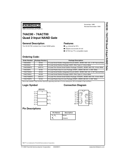
Device also available in Tape and Reel. Specify by appending suffix letter “X” to the ordering form. (PC not available in Tape and Reel.)
KK74AC299DW资料

TECHNICAL DATAKK 74AC2998-Bit Bidirectional Universal Shift Register with Parallel I/OHigh-Speed Silicon-Gate CMOSThe KK HC/HCT299. The device inputs are compatible with standard CMOS outputs; with pullup resistors, they are compatible with LS/ALS outputs. The KK 74AC299 features a multiplexed parallel input/output data port to achieve full 8-bit handling in a 20 pin package. Due to the large output drive capability and the 3-state feature, this device is ideally suited for interface with bus lines in a bus-oriented system.Two Mode-Select inputs and two Output Enable inputs are used to choose the mode of operation as listed in the Function Table.Synchronous parallel loading is accomplished by taking both Mode-Select lines, S 1 and S 2, high. This places the outputs in the high-impedance state, which permits data applied to the data port to be clockedinto the register. Reading out of the register can be accomplished whenthe outputs are enabled. The active-low asynchronous Reset overrides all other inputs.• Outputs Directly Interface to CMOS, NMOS, and TTL PIN ASSIGNMENT • Operating Voltage Range: 2.0 to 6.0 V• Low Input Current: 1.0 µA; 0.1 µA @ 25°C• High Noise Immunity Characteristic of CMOS Devices • Outputs Source/Sink 24 mALOGIC DIAGRAMPIN 20=V CC PIN 10 = GNDMAXIMUM RATINGS*Symbol Parameter ValueUnit V CC DC Supply Voltage (Referenced to GND) -0.5 to +7.0 VV IN DC Input Voltage (Referenced to GND) -0.5 to V CC +0.5 VV OUT DC Output Voltage (Referenced to GND) -0.5 to V CC +0.5 VI IN DC Input Current, per Pin ±20 mAI OUT DC Output Sink/Source Current, per Pin ±50 mAI CC DC Supply Current, V CC and GND Pins ±50 mAP D Power Dissipation in Still Air, Plastic DIP+ SOIC Package+ 750500mWTstg Storage Temperature -65 to +150 °CT L Lead Temperature, 1 mm from Case for 10 Seconds(Plastic DIP or SOIC Package)260 °C*Maximum Ratings are those values beyond which damage to the device may occur.Functional operation should be restricted to the Recommended Operating Conditions.+Derating - Plastic DIP: - 10 mW/°C from 65° to 125°CSOIC Package: : - 7 mW/°C from 65° to 125°CRECOMMENDED OPERATING CONDITIONSSymbol Parameter MinMaxUnit V CC DC Supply Voltage (Referenced to GND) 2.0 6.0 VV IN, V OUT DC Input Voltage, Output Voltage (Referenced to GND) 0 V CC VT J Junction Temperature (PDIP) 140 °CT A Operating Temperature, All Package Types -40 +85 °CI OH Output Current - High -24 mAI OL Output Current - Low 24 mAt r, t f Input Rise and Fall Time *(except Schmitt Inputs) V CC =3.0 VV CC =4.5 VV CC =5.5 V1504025ns/V* VINfrom 30% to 70% V CCThis device contains protection circuitry to guard against damage due to high static voltages or electric fields. However, precautions must be taken to avoid applications of any voltage higher than maximum rated voltages to this high-impedance circuit. For proper operation, V IN and V OUT should be constrained to the range GND≤(V IN or V OUT)≤V CC.Unused inputs must always be tied to an appropriate logic voltage level (e.g., either GND or V CC). Unused outputs must be left open.DC ELECTRICAL CHARACTERISTICS (Voltages Referenced to GND)V CC Guaranteed Limits Symbol Parameter TestConditions V25 °C -40°C to85°CUnitV IH Minimum High-Level Input Voltage V OUT=0.1 V or V CC-0.1 V 3.04.55.52.13.153.852.13.153.85VV IL Maximum Low -Level Input Voltage V OUT=0.1 V or V CC-0.1 V 3.04.55.50.91.351.650.91.351.65VV OH Minimum High-Level Output Voltage I OUT≤ -50 µA 3.04.55.52.94.45.42.94.45.4V*VIN=V IH or V ILI OH=-12 mAI OH=-24 mAI OH=-24 mA3.04.55.52.563.864.862.463.764.76V OL Maximum Low-Level Output Voltage I OUT≤ 50 µA 3.04.55.50.10.10.10.10.10.1V*VIN= V IH or V ILI OL=12 mAI OL=24 mAI OL=24 mA3.04.55.50.360.360.360.440.440.44I IN Maximum InputLeakage CurrentV IN=V CC or GND 5.5±0.1 ±1.0 µAI OZ Maximum Three-State LeakageCurrent V IN (OE)= V IH or V ILV IN =V CC or GNDV OUT =V CC or GND5.5±0.6 ±6.0 µAI OLD+Minimum DynamicOutput CurrentV OLD=1.65 V Max 5.575 mAI OHD+Minimum DynamicOutput CurrentV OHD=3.85 V Min 5.5-75 mAI CC Maximum QuiescentSupply Current(per Package)V IN=V CC or GND 5.58.0 80 µA* All outputs loaded; thresholds on input associated with output under test.+Maximum test duration 2.0 ms, one output loaded at a time.Note: I IN and I CC @ 3.0 V are guaranteed to be less than or equal to the respective limit @ 5.5 V V CCAC ELECTRICAL CHARACTERISTICS (C L=50pF,Input t r=t f=3.0 ns)V CC*Guaranteed LimitsSymbol Parameter V25 °C -40°C to85°CUnitMinMax MinMaxf max Maximum Clock Frequency (Figure 1) 3.35.09013080105MHzt PLH Propagation Delay, Clock to Q A’ or Q H’ (Figure 1) 3.35.08.55.520.514.07.04.522.015.0nst PHL Propagation Delay, Clock to Q A’ or Q H’ (Figure 1) 3.35.08.55.521.514.57.05.023.016.0nst PLH Propagation Delay, Clock to Q A thru Q H (Figure 1) 3.35.09.06.020.514.57.55.022.516.0nst PHL Propagation Delay, Clock to Q A thru Q H (Figure 1) 3.35.010.06.523.016.08.56.024.517.5nst PHL Propagation Delay, Reset to Q A’ or Q H’ (Figure 2) 3.35.09.05.522.515.57.55.025.017.0nst PHL Propagation Delay, Reset to Q A thru Q H (Figure 2) 3.35.09.05.521.515.07.55.024.016.5nst PZH Propagation Delay , OE1, OE2 to Q A thru Q H (Figure 3) 3.35.07.04.518.012.56.04.019.513.5nst PZL Propagation Delay , OE1, OE2 to Q A thru Q H (Figure 3) 3.35.07.05.018.012.56.04.020.514.0nst PHZ Propagation Delay , OE1, OE2 to Q A thru Q H (Figure 3) 3.35.06.53.518.514.05.53.019.515.0nst PLZ Propagation Delay , OE1, OE2 to Q A thru Q H (Figure 3) 3.35.05.53.517.012.54.52.019.013.5nsC IN Maximum Input Capacitance 5.0 4.5 4.5 pFTypical @25°C,V CC=5.0 VC PD Power Dissipation Capacitance 170 pF *Voltage Range 3.3 V is 3.3 V ±0.3 VVoltage Range 5.0 V is 5.0 V ±0.5 VTIMING REQUIREMENTS (C L=50pF,Input t r=t f=3.0 ns)V CC*Guaranteed Limits Symbol Parameter V25 °C -40°C to85°CUnitt su Minimum Setup Time, Mode Select S1 or S2 to Clock (Figure 4) 3.35.08.05.08.55.5nst su Minimum Setup Time, Data Inputs P A thru P H to Clock (Figure 4) 3.35.05.53.56.04.0nst su Minimum Setup Time, Data Inputs S A, S H to Clock (Figure 4) 3.35.06.54.07.04.5nst h Minimum Hold Time, Clock to Mode Select S1 or S2 (Figure 4) 3.35.00.51.00.51.0nst h Minimum Hold Time, Clock to Data Inputs P A thru P H (Figure 4) 3.35.01.01.0nst h Minimum Hold Time, Clock to Data Inputs S A, S H (Figure 4) 3.35.01.00.51.0nst rec Minimum Recovery Time, Reset Inactive to Clock (Figure 2) 3.35.01.51.51.51.5nst w Minimum Pulse Width, Clock (Figure 1) 3.35.04.53.55.03.5nst w Minimum Pulse Width, Reset (Figure 2) 3.35.04.53.55.03.5ns*Voltage Range 3.3 V is 3.3 V ±0.3 V Voltage Range 5.0 V is 5.0 V ±0.5 VFUNCTION TABLEZ = high impedanceD = data on serial inputF = flip-flop (see Logic Diagram)When one or both output controls are high the eight input/output terminals are disabled to the high- impedance state; however, sequential operation or clearing of the register is not affected.Figure 1. Switching Waveform Figure 2. Switching WaveformEXPANDED LOGIC DIAGRAM。
TC74ACT74FT资料

TOSHIBA CMOS Digital Integrated Circuit Silicon Monolithic TC74ACT74P,TC74ACT74F,TC74ACT74FN,TC74ACT74FT Dual D-Type Flip Flop with Preset and ClearThe TC74ACT74 is an advanced high speed CMOS D-FLIP FLOP fabricated with silicon gate and double-layer metal wiring C2MOS technology.It achieves the high speed operation similar to equivalent Bipolar Schottky TTL while maintaining the CMOS low power dissipation.This device may be used as a level converter for interfacing TTL or NMOS to High Speed CMOS. The inputs are compatible with TTL, NMOS and CMOS output voltage levels.The signal level applied to the D INPUT is transferred to Q OUTPUT during the positive going transition of the CK pulse. CLR and PR are independent of the CK and are accomplished by setting the appropriate input to an “L” level. All inputs are equipped with protection circuits against static discharge or transient excess voltage.Features•High speed: f max = 180 MHz (typ.) at V CC = 5 V•Low power dissipation: I CC = 4 μA (max) at Ta = 25°C •Compatible with TTL outputs: V IL = 0.8 V (max)V IH = 2.0 V (min) •Symmetrical output impedance: |I OH| = I OL = 24 mA (min)Capability of driving 50 Ωtransmission lines. •Balanced propagation delays: t pLH ∼ − t pHL•Pin and function compatible with 74F74 Note: xxxFN (JEDEC SOP) is not available in Japan.TC74ACT74PTC74ACT74FTC74ACT74FNTC74ACT74FTWeightDIP14-P-300-2.54 : 0.96 g (typ.) SOP14-P-300-1.27A : 0.18 g (typ.) SOL14-P-150-1.27 : 0.12 g (typ.) TSSOP14-P-0044-0.65A : 0.06 g (typ.)Pin AssignmentIEC Logic SymbolTruth TableX: Don’t careSystem DiagramQ 1PR1V CCCLR 22D 2CK PR 2 2QCLR11D 1CK1QQ 29 814 13 12 11 10 (top view) GNDCLR2CLR 1(12)(3)S (4)(1)(2)(11)(10)1CK PR 11D 2CK 2D (5) (6) (9) (8)1QQ 12QQ2C11D R(13)PR 2DCLR CKPRQQφϕAbsolute Maximum Ratings (Note 1)Characteristics Symbol Rating Unit Supply voltage range V CC−0.5 to 7.0 VDC input voltage V IN−0.5 to V CC + 0.5 VDC output voltage V OUT−0.5 to V CC + 0.5 VmA Input diode current I IK ±20Output diode current I OK ±50 mA DC output current I OUT ±50 mA DC V CC/ground current I CC ±100 mA Power dissipation P D500 (DIP) (Note 2)/180 (SOP/TSSOP) mWStorage temperature T stg−65 to 150 °CNote 1: Exceeding any of the absolute maximum ratings, even briefly, lead to deterioration in IC performance or even destruction.Using continuously under heavy loads (e.g. the application of high temperature/current/voltage and thesignificant change in temperature, etc.) may cause this product to decrease in the reliability significantlyeven if the operating conditions (i.e. operating temperature/current/voltage, etc.) are within the absolutemaximum ratings and the operating ranges.Please design the appropriate reliability upon reviewing the Toshiba Semiconductor Reliability Handbook(“Handling Precautions”/“Derating Concept and Methods”) and individual reliability data (i.e. reliability testreport and estimated failure rate, etc).Note 2: 500 mW in the range of Ta = −40°C to 65°C. From Ta = 65°C to 85°C a derating factor of −10 mW/°C should be applied up to 300 mW.Operating Ranges (Note)Characteristics Symbol Rating Unit Supply voltage V CC 4.5 to 5.5 VInput voltage V IN0 to V CC VOutput voltage V OUT0 to V CC VOperating temperature T opr−40 to 85 °CInput rise and fall time dt/dV 0 to 10 ns/VNote: The operating ranges must be maintained to ensure the normal operation of the device.Unused inputs must be tied to either VCC or GND.Electrical CharacteristicsDC CharacteristicsTest ConditionTa = 25°CTa = −40 to 85°CCharacteristics SymbolV CC (V)Min Typ.Max Min MaxUnitHigh-level input voltage V IH― 4.5 to 5.5 2.0―― 2.0 ― VLow-level input voltageV IL―4.5 to5.5― ― 0.8 ― 0.8 V High-level output voltageV OHV IN= V IH or V ILI OH = −50 μAI OH = −24 mA I OH = −75 mA (Note) 4.54.55.5 4.4 3.94― 4.5 ― ― ― ― ― 4.4 3.80 3.85 ― ― ― VLow-level output voltage V OLVIN= V IH or V ILI OL = 50 μAI OL = 24 mA I OL = 75 mA (Note) 4.54.55.5― ― ― 0.0 ― ―0.1 0.36 ―― ― ―0.1 0.441.65V Input leakage currentI IN V IN = V CC or GND 5.5― ― ±0.1 ― ±1.0μA I CC V IN = V CC or GND 5.5― ― 4.0 ― 40.0μA Quiescent supply currentI CPer input: V IN = 3.4 V Other input: V CC or GND5.5―― 1.35 ― 1.5 mANote: This spec indicates the capability of driving 50 Ω transmission lines. One output should be tested at a time for a 10 ms maximum duration.Timing Requirements (input: t r = t f = 3 ns)AC Characteristics (C L = 50 pF, R L = 500 Ω, input: t r = t f = 3 ns)Note: C PD is defined as the value of the internal equivalent capacitance which is calculated from the operating current consumption without load.Average operating current can be obtained by the equation:I CC (opr) = C PD·V CC·f IN + I CC/2 (per F/F)Weight: 0.96 g (typ.)Weight: 0.18 g (typ.)Package Dimensions (Note)Note: This package is not available in Japan. Weight: 0.12 g (typ.)Package DimensionsWeight: 0.06 g (typ.)RESTRICTIONS ON PRODUCT USE20070701-EN GENERAL •The information contained herein is subject to change without notice.•TOSHIBA is continually working to improve the quality and reliability of its products. Nevertheless, semiconductor devices in general can malfunction or fail due to their inherent electrical sensitivity and vulnerability to physical stress. It is the responsibility of the buyer, when utilizing TOSHIBA products, to comply with the standards of safety in making a safe design for the entire system, and to avoid situations in which a malfunction or failure of such TOSHIBA products could cause loss of human life, bodily injury or damage to property.In developing your designs, please ensure that TOSHIBA products are used within specified operating ranges as set forth in the most recent TOSHIBA products specifications. Also, please keep in mind the precautions and conditions set forth in the “Handling Guide for Semiconductor Devices,” or “TOSHIBA Semiconductor Reliability Handbook” etc.• The TOSHIBA products listed in this document are intended for usage in general electronics applications (computer, personal equipment, office equipment, measuring equipment, industrial robotics, domestic appliances, etc.).These TOSHIBA products are neither intended nor warranted for usage in equipment that requires extraordinarily high quality and/or reliability or a malfunction or failure of which may cause loss of human life or bodily injury (“Unintended Usage”). Unintended Usage include atomic energy control instruments, airplane or spaceship instruments, transportation instruments, traffic signal instruments, combustion control instruments, medical instruments, all types of safety devices, etc.. Unintended Usage of TOSHIBA products listed in his document shall be made at the customer’s own risk.•The products described in this document shall not be used or embedded to any downstream products of which manufacture, use and/or sale are prohibited under any applicable laws and regulations.• The information contained herein is presented only as a guide for the applications of our products. No responsibility is assumed by TOSHIBA for any infringements of patents or other rights of the third parties which may result from its use. No license is granted by implication or otherwise under any patents or other rights of TOSHIBA or the third parties.• Please contact your sales representative for product-by-product details in this document regarding RoHS compatibility. Please use these products in this document in compliance with all applicable laws and regulations that regulate the inclusion or use of controlled substances. Toshiba assumes no liability for damage or losses occurring as a result of noncompliance with applicable laws and regulations.。
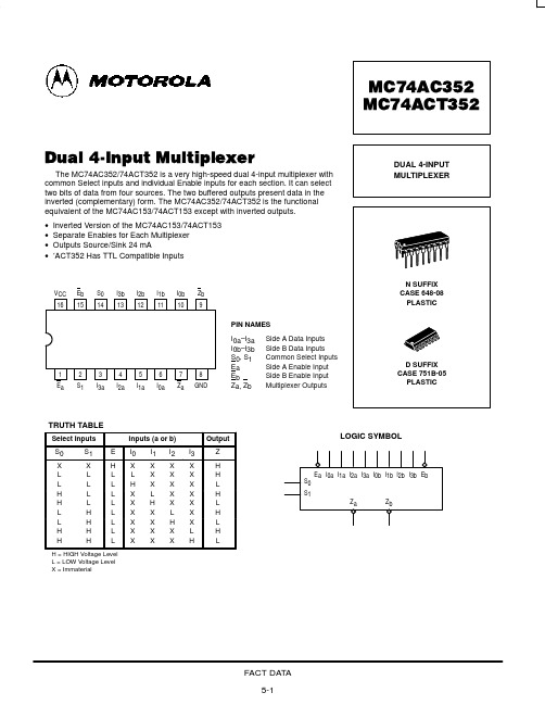
MC74ACT352D中文资料
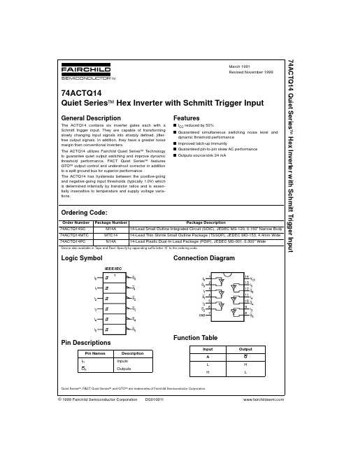
74ACTQ14MTC资料
Note 1: Absolute maximum ratings are those values beyond which damage to the device may occur. The databook specifications should be met, without exception, to ensure that the system design is reliable over its power supply, temperature, and output/input loading variables. Fairchild does not recommend operation outside of databook specifications.
Recommended Operating Conditions
Supply Voltage (VCC) Input Voltage (VI) Output Voltage (VO) Operating Temperature (TA) 4.5V to 5.5 0V to VCC 0V to VCC −40°C to +85°C
Ordering Code:
Order Number 74ACTQ14SC 74ACTQ14MTC 74ACTQ14PC Package Number M14A MTC14 N14A Package Description 14-Lead Small Outline Integrated Circuit (SOIC), JEDEC MS-120, 0.150” Narrow Body 14-Lead Thin Shrink Small Outline Package (TSSOP), JEDEC MO-153, 4.4mm Wide 14-Lead Plastic Dual-In-Lead Package (PDIP), JEDEC MS-001, 0.300” Wide
KK74VHC00中文资料
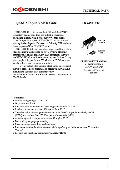
TECHNICAL DATAKK 74VHC00Quad 2-Input NAND GateKK 74VHC00 is high-speed logic IC made by CMOS technology and designed for use in high-performance calculating systems with a wide supply voltage range. As for operation speed, KK 74VHC00 can be compared with equivalent bipolar ICs based on Schottky TTL and two times surpasses ICs of KK 74НС series.KK 74VHC00 tolerates operation under conditions when voltage on input is exceeded up to 7V without affecting characteristics and IC reliability. This possibility allows to use KK 74VHC00 in radio-electronic devices for interfacing with supply voltages 5V and 3V, eliminate IC failure under supply voltage source emergency outage.Use of output edge shaping block in the microcircuit allows to reduce noise amplitude of noises when switching outputs into the same state simultaneously.Input and output levels of KK 74VHC00 are compatible with CMOS levelsFeatures:• Supply voltage range 2.0 to 5.5 V. • Output current 8 mA.• Low consumption current: 0.2 mkA (typical value) at Та = 25 °С. • Latchup current not less than 300 mA at Та = 85 °С.• Tolerable value of static potential not less than 2000 V as per human body model (HBM) and not less than 200 V as per machine model (ММ). • Ambient operation temperature minus 40 to plus 85°С. • Balanced signal propagation delay.• Ensures voltage exceeding mode on input• Low noise level at the simultaneous switching of outputs in the same state: V OLP = 0.8 V (max).• For pins and functions, compatible with KK 74НС00..KK74VHC00 truth tablePins description in KK74VHC00Absolute maximum conditions*Parameter, unit Symbol Valueminmax Supply voltage, V V CC-0.5 7.0Input voltage, V Vin -0.5 7.0Output voltage, V Vout -0.5 Vcc+0.5VInput diode current, mA Iik – -20Current of common output and supplyoutput, mAIcc – ± 75Output current, mA Iout – ± 25Output diode current, mA Iok – ± 20Dissipated power, mW Pd – 180*Under absolute maximum conditions operation of microcircuit is not guaranteed. Operation isguaranteed under maximum conditionsMaximum conditionsSymbol ValueParameter, unitminmax Supply voltage, V V CC 2.0 5.5Input voltage,V Vin 0 V CCOutput voltage, V Vout 0 V CCOutput current, mA Iout – ± 8.0Input rise and fall time, ns/V at Vcc = (3.3 ± 0.3) Vat Vcc = (5.0 ± 0.5) V t LH, t HL10020DC electrical characteristicsValue25 °C–40 to 85 °CSymbo l Parameter Test conditionsV CC ,V min max min maxUnit 2.01.5 – 1.5 – VV IHHigh input voltage–3.0-5.50.7Vcc– 0.7Vcc –2.0 – 0.5 – 0.5 V IL Low input voltage–3.0-5.5– 0.3Vcc – 0.3Vcc2.0 1.92– 1.9 –3.0 2.92– 2.9 –4.5 4.42– 4.4 – V I = V IH or V IL I O = -50 mkA5.5 5.52– 5.4 –V I = V IH or V IL ; I O = -4 mA3.0 2.58– 2.48 –V OHHigh output voltage V I = V IH or V IL ; I O = -8 mA4.5 3.94– 3.80 –2.0 – 0.09– 0.13.0 – 0.09– 0.14.5 – 0.09– 0.1 V I =V IH orV IL I O = 50 mkA 5.5 – 0.09– 0.1V I = V IH or V IL I O = 4 mA 3.0 – 0.36– 0.44V OLLow output voltage V I = V IH or V IL I O = 8 mA4.5 – 0.36– 0.44I OZ Output current in "off" stateV I = V IH or V IL V O = V CC or 0V 5.5 - ±0.25- ±2.5mkA I I Input current V I = 5.5V or 0V 0 – 5.5- ±0.1- ±1.0I CCConsumption current V I =V CC or 0V5.5 - 4.0 - 40.0AC electrical characteristics (t LH = t HL = 3.0 ns)Value25 °C–40to 85 °CSymbol Parameter Testconditi ons V CC , VC L , pF min max min maxUnit 15- 7.9- 9.5 3.3 ± 0.350 11.4 13.0 155.56.5 t PHL , t PLHPropagation delay time when switching "on", "off" Figure 2 5.0 ± 0.550 7.5 8.5ns C I Input capacity - 5.0 10 -C РDDynamic capacity V I = 0 V orV CC5.0 38 -pFNoise characteristics (C L = 50 pF)ValueSymbol Parameter V CC , V min maxUnit V OLP Positive noise of low output voltage 5.0 - 0.8 V V OLV Negative noise of low output voltage5.0 -0.8 - V IHD Input dynamic high voltage 5.0 3.5 - V ILDInput dynamic low voltage5.0-1.5- Time diagram of input and output pulsesVССGNDVCC0 V。
SN74AC533NSRE4中文资料
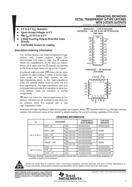
PACKAGING INFORMATIONOrderable Device Status (1)Package Type Package Drawing Pins Package Qty Eco Plan (2)Lead/Ball FinishMSL Peak Temp (3)SN74AC533DBLE OBSOLETE SSOP DB 20TBDCall TI Call TISN74AC533DBR ACTIVE SSOP DB 202000Green (RoHS &no Sb/Br)CU NIPDAU Level-1-260C-UNLIM SN74AC533DBRE4ACTIVE SSOP DB 202000Green (RoHS &no Sb/Br)CU NIPDAU Level-1-260C-UNLIM SN74AC533DBRG4ACTIVE SSOP DB 202000Green (RoHS &no Sb/Br)CU NIPDAU Level-1-260C-UNLIM SN74AC533DWACTIVE SOIC DW 2025Green (RoHS &no Sb/Br)CU NIPDAU Level-1-260C-UNLIM SN74AC533DWG4ACTIVE SOIC DW 2025Green (RoHS &no Sb/Br)CU NIPDAU Level-1-260C-UNLIM SN74AC533DWR ACTIVE SOIC DW 202000Green (RoHS &no Sb/Br)CU NIPDAU Level-1-260C-UNLIM SN74AC533DWRE4ACTIVE SOIC DW 202000Green (RoHS &no Sb/Br)CU NIPDAU Level-1-260C-UNLIM SN74AC533DWRG4ACTIVE SOIC DW 202000Green (RoHS &no Sb/Br)CU NIPDAU Level-1-260C-UNLIM SN74AC533N ACTIVE PDIP N 2020Pb-Free (RoHS)CU NIPDAU N /A for Pkg Type SN74AC533NE4ACTIVE PDIP N 2020Pb-Free (RoHS)CU NIPDAU N /A for Pkg Type SN74AC533NSR ACTIVE SO NS 202000Green (RoHS &no Sb/Br)CU NIPDAU Level-1-260C-UNLIM SN74AC533NSRE4ACTIVE SO NS 202000Green (RoHS &no Sb/Br)CU NIPDAU Level-1-260C-UNLIM SN74AC533NSRG4ACTIVE SO NS 202000Green (RoHS &no Sb/Br)CU NIPDAU Level-1-260C-UNLIM SN74AC533PW ACTIVE TSSOP PW 2070Green (RoHS &no Sb/Br)CU NIPDAU Level-1-260C-UNLIM SN74AC533PWE4ACTIVE TSSOP PW 2070Green (RoHS &no Sb/Br)CU NIPDAU Level-1-260C-UNLIM SN74AC533PWG4ACTIVE TSSOP PW 2070Green (RoHS &no Sb/Br)CU NIPDAU Level-1-260C-UNLIM SN74AC533PWLE OBSOLETE TSSOP PW 20TBDCall TI Call TISN74AC533PWR ACTIVE TSSOP PW 202000Green (RoHS &no Sb/Br)CU NIPDAU Level-1-260C-UNLIM SN74AC533PWRE4ACTIVE TSSOP PW 202000Green (RoHS &no Sb/Br)CU NIPDAU Level-1-260C-UNLIM SN74AC533PWRG4ACTIVETSSOPPW202000Green (RoHS &no Sb/Br)CU NIPDAULevel-1-260C-UNLIM(1)The marketing status values are defined as follows:ACTIVE:Product device recommended for new designs.LIFEBUY:TI has announced that the device will be discontinued,and a lifetime-buy period is in effect.NRND:Not recommended for new designs.Device is in production to support existing customers,but TI does not recommend using this part in a new design.PREVIEW:Device has been announced but is not in production.Samples may or may not be available.OBSOLETE:TI has discontinued the production of the device.(2)Eco Plan -The planned eco-friendly classification:Pb-Free (RoHS),Pb-Free (RoHS Exempt),or Green (RoHS &no Sb/Br)-please check /productcontent for the latest availability information and additional product content details.4-Jun-2007TBD:The Pb-Free/Green conversion plan has not been defined.Pb-Free (RoHS):TI's terms "Lead-Free"or "Pb-Free"mean semiconductor products that are compatible with the current RoHS requirements for all 6substances,including the requirement that lead not exceed 0.1%by weight in homogeneous materials.Where designed to be soldered at high temperatures,TI Pb-Free products are suitable for use in specified lead-free processes.Pb-Free (RoHS Exempt):This component has a RoHS exemption for either 1)lead-based flip-chip solder bumps used between the die and package,or 2)lead-based die adhesive used between the die and leadframe.The component is otherwise considered Pb-Free (RoHS compatible)as defined above.Green (RoHS &no Sb/Br):TI defines "Green"to mean Pb-Free (RoHS compatible),and free of Bromine (Br)and Antimony (Sb)based flame retardants (Br or Sb do not exceed 0.1%by weight in homogeneous material)(3)MSL,Peak Temp.--The Moisture Sensitivity Level rating according to the JEDEC industry standard classifications,and peak solder temperature.Important Information and Disclaimer:The information provided on this page represents TI's knowledge and belief as of the date that it is provided.TI bases its knowledge and belief on information provided by third parties,and makes no representation or warranty as to the accuracy of such information.Efforts are underway to better integrate information from third parties.TI has taken and continues to take reasonable steps to provide representative and accurate information but may not have conducted destructive testing or chemical analysis on incoming materials and chemicals.TI and TI suppliers consider certain information to be proprietary,and thus CAS numbers and other limited information may not be available for release.In no event shall TI's liability arising out of such information exceed the total purchase price of the TI part(s)at issue in this document sold by TI to Customer on an annualbasis.4-Jun-2007TAPE AND REELINFORMATION19-May-2007DevicePackage Pins SiteReel Diameter (mm)Reel Width (mm)A0(mm)B0(mm)K0(mm)P1(mm)W (mm)Pin1Quadrant SN74AC533DBR DB 20MLA 330168.27.5 2.51216Q1SN74AC533DWR DW 20MLA 3302410.813.0 2.71224Q1SN74AC533NSRNS 20MLA 330248.213.0 2.51224Q1SN74AC533PWRPW20MLA330166.957.11.6816Q1TAPE AND REEL BOX INFORMATIONDevice Package Pins Site Length (mm)Width (mm)Height (mm)SN74AC533DBR DB 20MLA 342.9336.628.58SN74AC533DWR DW 20MLA 333.2333.231.75SN74AC533NSR NS 20MLA 333.2333.231.75SN74AC533PWRPW20MLA342.9336.628.5819-May-200719-May-2007IMPORTANT NOTICETexas Instruments Incorporated and its subsidiaries(TI)reserve the right to make corrections,modifications,enhancements, improvements,and other changes to its products and services at any time and to discontinue any product or service without notice. Customers should obtain the latest relevant information before placing orders and should verify that such information is current and complete.All products are sold subject to TI’s terms and conditions of sale supplied at the time of order acknowledgment.TI warrants performance of its hardware products to the specifications applicable at the time of sale in accordance with TI’s standard warranty.Testing and other quality control techniques are used to the extent TI deems necessary to support this warranty.Except where mandated by government requirements,testing of all parameters of each product is not necessarily performed.TI assumes no liability for applications assistance or customer product design.Customers are responsible for their products and applications using TI components.To minimize the risks associated with customer products and applications,customers should provide adequate design and operating safeguards.TI does not warrant or represent that any license,either express or implied,is granted under any TI patent right,copyright,mask work right,or other TI intellectual property right relating to any combination,machine,or process in which TI products or services are rmation published by TI regarding third-party products or services does not constitute a license from TI to use such products or services or a warranty or endorsement e of such information may require a license from a third party under the patents or other intellectual property of the third party,or a license from TI under the patents or other intellectual property of TI. Reproduction of TI information in TI data books or data sheets is permissible only if reproduction is without alteration and is accompanied by all associated warranties,conditions,limitations,and notices.Reproduction of this information with alteration is an unfair and deceptive business practice.TI is not responsible or liable for such altered rmation of third parties may be subject to additional restrictions.Resale of TI products or services with statements different from or beyond the parameters stated by TI for that product or service voids all express and any implied warranties for the associated TI product or service and is an unfair and deceptive business practice.TI is not responsible or liable for any such statements.TI products are not authorized for use in safety-critical applications(such as life support)where a failure of the TI product would reasonably be expected to cause severe personal injury or death,unless officers of the parties have executed an agreement specifically governing such use.Buyers represent that they have all necessary expertise in the safety and regulatory ramifications of their applications,and acknowledge and agree that they are solely responsible for all legal,regulatory and safety-related requirements concerning their products and any use of TI products in such safety-critical applications,notwithstanding any applications-related information or support that may be provided by TI.Further,Buyers must fully indemnify TI and its representatives against any damages arising out of the use of TI products in such safety-critical applications.TI products are neither designed nor intended for use in military/aerospace applications or environments unless the TI products are specifically designated by TI as military-grade or"enhanced plastic."Only products designated by TI as military-grade meet military specifications.Buyers acknowledge and agree that any such use of TI products which TI has not designated as military-grade is solely at the Buyer's risk,and that they are solely responsible for compliance with all legal and regulatory requirements in connection with such use.TI products are neither designed nor intended for use in automotive applications or environments unless the specific TI products are designated by TI as compliant with ISO/TS16949requirements.Buyers acknowledge and agree that,if they use anynon-designated products in automotive applications,TI will not be responsible for any failure to meet such requirements. Following are URLs where you can obtain information on other Texas Instruments products and application solutions:Products ApplicationsAmplifiers Audio /audioData Converters Automotive /automotiveDSP Broadband /broadbandInterface Digital Control /digitalcontrolLogic Military /militaryPower Mgmt Optical Networking /opticalnetworkMicrocontrollers Security /securityRFID Telephony /telephonyLow Power /lpw Video&Imaging /videoWirelessWireless /wirelessMailing Address:Texas Instruments,Post Office Box655303,Dallas,Texas75265Copyright©2007,Texas Instruments Incorporated。
KK74HCT00AN资料
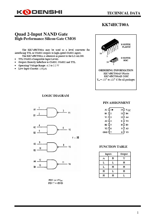
TECHNICAL DATAKK 74HCT00AQuad 2-Input NAND GateHigh-Performance Silicon-Gate CMOSThe KK 74HCT00A may be used as a level converter for interfacing TTL or NMOS outputs to high-speed CMOS inputs.The KK 74HCT00A is identical in pinout to the LS/ALS00. • TTL/NMOS-Compatible Input Levels.• Outputs Directly Inferface to CMOS, NMOS and TTL. • Operating Voltage Range: 4.5 to 5.5 V • Low Input Current: 1.0 µALOGIC DIAGRAMPIN 14 =V CC PIN 7 = GNDPIN ASSIGNMENTFUNCTION TABLEInputs Output A B Y L L H L H HH L H H H LMAXIMUM RATINGS*Symbol Parameter ValueUnit V CC DC Supply Voltage (Referenced to GND) -0.5 to +7.0 VV IN DC Input Voltage (Referenced to GND) -1.5 to V CC +1.5 VV OUT DC Output Voltage (Referenced to GND) -0.5 to V CC +0.5 VI IN DC Input Current, per Pin ±20 mAI OUT DC Output Current, per Pin ±25 mAI CC DC Supply Current, V CC and GND Pins ±50 mAP D Power Dissipation in Still Air, Plastic DIP+ SOIC Package+ 750500mWTstg Storage Temperature -65 to +150 °CT L Lead Temperature, 1 mm from Case for 10 Seconds(Plastic DIP or SOIC Package)260 °C*Maximum Ratings are those values beyond which damage to the device may occur.Functional operation should be restricted to the Recommended Operating Conditions.+Derating - Plastic DIP: - 10 mW/°C from 65° to 125°CSOIC Package: : - 7 mW/°C from 65° to 125°CRECOMMENDED OPERATING CONDITIONSSymbol Parameter MinMaxUnit V CC DC Supply Voltage (Referenced to GND) 4.5 5.5 VV IN, V OUT DC Input Voltage, Output Voltage (Referenced to GND) 0 V CC VT A Operating Temperature, All Package Types -55 +125 °Ct r, t f Input Rise and Fall Time (Figure 1) 0 500 nsThis device contains protection circuitry to guard against damage due to high static voltages or electric fields.However, precautions must be taken to avoid applications of any voltage higher than maximum rated voltages to thishigh-impedance circuit. For proper operation, V IN and V OUT should be constrained to the range GND≤(V IN orV OUT)≤V CC.Unused inputs must always be tied to an appropriate logic voltage level (e.g., either GND or V CC). Unusedoutputs must be left open.DC ELECTRICAL CHARACTERISTICS (Voltages Referenced to GND)V CC Guaranteed LimitSymbol Parameter TestConditions V25 °Cto-55°C ≤85°C≤125°CUnitV IH Minimum High-Level Input Voltage V OUT=0.1 V or V CC-0.1 V⎢I OUT⎢≤ 20 µA4.55.52.02.02.02.02.02.0VV IL Maximum Low -Level Input Voltage V OUT= V CC-0.1 V⎢I OUT⎢≤ 20 µA4.55.50.80.80.80.80.80.8VV OH Minimum High-Level Output Voltage V IN=V IH or V IL⎢I OUT⎢≤ 20 µA4.55.54.45.44.45.44.45.4VV IN=V IH or V IL⎢I OUT⎢≤ 4.0 mA 4.5 3.98 3.84 3.7V OL Maximum Low-Level Output Voltage V IN=V IH⎢I OUT⎢≤ 20 µA4.55.50.10.10.10.10.10.1VV IN=V IH⎢I OUT⎢≤ 4.0 mA 4.50.26 0.33 0.4I IN Maximum InputLeakage CurrentV IN=V CC or GND 5.5±0.1 ±1.0 ±1.0 µAI CC Maximum QuiescentSupply Current(per Package) V IN=V CC or GNDI OUT=0µA5.5 1.0 10 40 µA∆I CC Additional QuiescentSupply Current V IN = 2.4 V, Any One Input ≥-55°C 25°C to125°CmAV IN=V CC or GND, OtherInputsI OUT=0µA5.5 2.9 2.4AC ELECTRICAL CHARACTERISTICS (V CC=5.0 V ± 10%, C L=50pF, Input t r=t f=6.0 ns)GuaranteedLimits Symbol Parameter 25 °C to-55°C≤85°C ≤125°C Unitt PLH, t PHL Maximum Propagation Delay, Input A or B to Output Y (Figures 1 and 2) 19 2428nst TLH, t THL Maximum Output Transition Time, Any Output (Figures 1 and 2) 15 1922nsC IN Maximum Input Capacitance 10 10 10 pFPower Dissipation Capacitance (Per Gate) Typical @25°C,V CC=5.0 VC PD Used to determine the no-load dynamic powerconsumption:P D=C PD V CC2f+I CC V CC15 pFFigure 1. Switching Waveforms Figure 2. Test CircuitEXPANDED LOGIC DIAGRAM(1/4 of the Device)。
74ACT74T资料
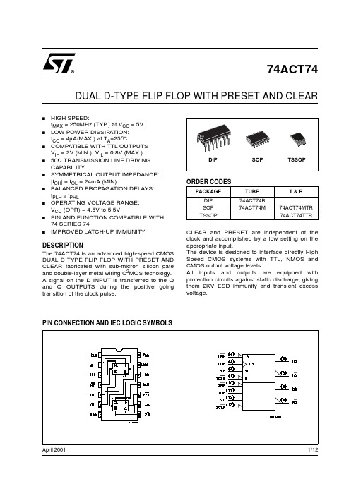
1/12April 2001sHIGH SPEED:f MAX = 250MHz (TYP.) at V CC = 5V sLOW POWER DISSIPATION:I CC = 4µA(MAX.) at T A =25°CsCOMPATIBLE WITH TTL OUTPUTS V IH = 2V (MIN.), V IL = 0.8V (MAX.)s50Ω TRANSMISSION LINE DRIVING CAPABILITYsSYMMETRICAL OUTPUT IMPEDANCE:|I OH | = I OL = 24mA (MIN)sBALANCED PROPAGATION DELAYS:t PLH ≅ t PHLsOPERATING VOLTAGE RANGE:V CC (OPR) = 4.5V to 5.5VsPIN AND FUNCTION COMPATIBLE WITH 74 SERIES 74sIMPROVED LATCH-UP IMMUNITYDESCRIPTIONThe 74ACT74 is an advanced high-speed CMOS DUAL D-TYPE FLIP FLOP WITH PRESET AND CLEAR fabricated with sub-micron silicon gate and double-layer metal wiring C 2MOS tecnology. A signal on the D INPUT is transferred to the Q and Q OUTPUTS during the positive going transition of the clock pulse.CLEAR and PRESET are independent of the clock and accomplished by a low setting on the appropriate input.The device is designed to interface directly High Speed CMOS systems with TTL, NMOS and CMOS output voltage levels.All inputs and outputs are equipped with protection circuits against static discharge, giving them 2KV ESD immunity and transient excess voltage.74ACT74DUAL D-TYPE FLIP FLOP WITH PRESET AND CLEARPIN CONNECTION AND IEC LOGIC SYMBOLSORDER CODESPACKAGE TUBE T & R DIP 74ACT74B SOP 74ACT74M74ACT74MTR TSSOP74ACT74TTR74ACT742/12INPUT AND OUTPUT EQUIVALENT CIRCUITPIN DESCRIPTIONTRUTH TABLELOGIC DIAGRAMThis logic diagram has not be used to estimate propagation delaysPIN No SYMBOL NAME AND FUNCTION 1, 131CLR, 2CLR Asyncronous Reset - Direct Input 2, 121D, 2D Data Inputs 3, 111CK, 2CKClock Input(LOW to HIGH, Edge Triggered)4, 101PR, 2PR Asyncronous Set - Direct Input5, 91Q, 2Q True Flip-Flop Outputs 6, 81Q, 2Q Complement Flip-Flop Outputs 7GND Ground (0V)14V CCPositive Supply Voltage74ACT743/12ABSOLUTE MAXIMUM RATINGSAbsolute Maximum Ratings are those values beyond which damage to the device may occur. Functional operation under these conditions is not implied.RECOMMENDED OPERATING CONDITIONS1) V IN from 0.8V to 2.0VSymbol ParameterValue Unit V CC Supply Voltage -0.5 to +7V V I DC Input Voltage -0.5 to V CC + 0.5V V O DC Output Voltage -0.5 to V CC + 0.5V I IK DC Input Diode Current ± 20mA I OK DC Output Diode Current ± 20mA I O DC Output Current ± 50mA I CC or I GND DC V CC or Ground Current± 200mA T stg Storage Temperature -65 to +150°C T LLead Temperature (10 sec)300°CSymbol ParameterValue Unit V CC Supply Voltage 4.5 to 5.5V V I Input Voltage 0 to V CC V V O Output Voltage 0 to V CC V T op Operating Temperature-55 to 125°C dt/dvInput Rise and Fall Time V CC = 4.5 to 5.5V (note 1)8ns/V74ACT744/12DC SPECIFICATIONS1) Maximum test duration 2ms, one output loaded at time2) Incident wave switching is guaranteed on transmission lines with impedances as low as 50ΩAC ELECTRICAL CHARACTERISTICS (C L = 50 pF, R L = 500 Ω, Input t r = t f = 3ns)(*) Voltage range is 5.0V ± 0.5VSymbolParameterTest ConditionValue UnitV CC (V)T A = 25°C -40 to 85°C -55 to 125°C Min.Typ.Max.Min.Max.Min.Max.V IH High Level Input Voltage4.5V O = 0.1 V or V CC -0.1V 2.0 1.5 2.0 2.0V5.5 2.01.52.02.0V IL Low Level Input Voltage4.5V O = 0.1 V or V CC -0.1V 1.50.80.80.85.5 1.50.80.80.8VV OHHigh Level Output Voltage4.5I O =-50 µA 4.4 4.49 4.4 4.45.5I O =-50 µA 5.4 5.495.4 5.44.5I O =-24 mA 3.86 3.76 3.7V5.5I O =-24 mA 4.864.764.7V OLLow Level Output Voltage4.5I O =50 µA 0.0010.10.10.15.5I O =50 µA 0.0010.10.10.14.5I O =24 mA 0.360.440.55.5I O =24 mA 0.360.440.5I I Input Leakage Cur-rent5.5V I = V CC or GND ± 0.1± 1± 1µA I CCT Max I CC /Input 5.5V I = V CC - 2.1V 0.61.5 1.6mA I CC Quiescent Supply Current5.5V I = V CC or GND 44040µA I OLD Dynamic Output Current (note 1, 2)5.5V OLD = 1.65 V max 7550mA I OHDV OHD = 3.85 V min-75-50mA SymbolParameterTest ConditionValue UnitV CC (V)T A = 25°C -40 to 85°C -55 to 125°C Min.Typ.Max.Min.Max.Min.Max.t PLH t PHL Propagation DelayTime CK to Q or Q5.0(*) 5.010.011.011.0ns t PLH t PHL Propagation DelayTime PR or CLR to Q or Q5.0(*) 5.010.011.011.0ns t W Pulse Width HIGHor LOW, CK or PR or CLR5.0(*) 1.5 5.06.0 6.0ns t sSetup Time D to CK HIGH or LOW5.0(*)0.5 3.0 3.5 3.5ns t h Hold Time D to CKHIGH or LOW5.0(*)-0.5 1.0 1.0 1.0ns t REM Removal Tim|PR or CLR to CK5.0(*)-0.7 1.01.01.0ns f MAX Maximum ClockFrequency5.0(*)1002508585MHz74ACT745/12CAPACITIVE CHARACTERISTICS1) C PD is defined as the value of the IC’s internal equivalent capacitance which is calculated from the operating current consumption without load. (Refer to Test Circuit). Average operating current can be obtained by the following equation. I CC(opr) = C PD x V CC x f IN + I CC /2 (per Flip-Flop)TEST CIRCUITC L = 50pF or equivalent (includes jig and probe capacitance)R L = R 1 = 500Ω or equivalentR T = Z OUT of pulse generator (typically 50Ω)SymbolParameterTest ConditionValue UnitV CC (V)T A = 25°C -40 to 85°C -55 to 125°C Min.Typ.Max.Min.Max.Min.Max.C IN Input Capacitance 5.03pF C PDPower Dissipation Capacitance (note 1)5.0f IN = 10MHz43pF74ACT746/12WAVEFORM 1: PROPAGATION DELAYS, SETUP AND HOLD TIMES(f=1MHz; 50% duty cycle)74ACT747/12WAVEFORM 2: PROPAGATION DELAYS(f=1MHz; 50% duty cycle)74ACT74WAVEFORM 3: RECOVERY TIMES (f=1MHz; 50% duty cycle)WAVEFORM 4: PULSE WIDTH8/1274ACT74Information furnished is believed to be accurate and reliable. However, STMicroelectronics assumes no responsibility for the consequences of use of such information nor for any infringement of patents or other rights of third parties which may result from its use. No license is granted by implication or otherwise under any patent or patent rights of STMicroelectronics. Specifications mentioned in this publication are subject to change without notice. This publication supersedes and replaces all information previously supplied. STMicroelectronics products are not authorized for use as critical components in life support devices or systems without express written approval of STMicroelectronics.© The ST logo is a registered trademark of STMicroelectronics© 2001 STMicroelectronics - Printed in Italy - All Rights ReservedSTMicroelectronics GROUP OF COMPANIESAustralia - Brazil - China - Finland - France - Germany - Hong Kong - India - Italy - Japan - Malaysia - Malta - MoroccoSingapore - Spain - Sweden - Switzerland - United Kingdom© 12/12。
74ACT139PC中文资料

Features
s ICC reduced by 50% s Multifunction capability s Two completely independent 1-of-4 decoders s Active LOW mutually exclusive outputs s Outputs source/sink 24 mA s ACT139 has TTL-compatible inputs
FACT is a trademark of Fairchild Semiconductor Corporation.
© 1999 Fairchild Semiconductor Corporation
DS009926
元器件交易网
Device also available in Tape and Reel. Specify by appending suffix letter “X” to the ordering code.
Connection Diagram
Pin Descriptions
Pin Names A0, A1 E O0–O3 Description Address Inputs Enable Inputs Outputs
元器件交易网
74AC139 • 74ACT139 Dual 1-of-4 Decoder/Demultiplexer
November 1988 Revised November 1999
74AC139 • 74ACT139 Dual 1-of-4 Decoder/Demultiplexer
Recommended Operating Conditions
Supply Voltage (VCC) AC ACT Input Voltage (VI) Output Voltage (VO) Operating Temperature (TA) Minimum Input Edge Rate (∆V/∆t) AC Devices VIN from 30% to 70% of VCC VCC @ 3.3V, 4.5V, 5.5V Minimum Input Edge Rate (∆V/∆t) ACT Devices VIN from 0.8V to 2.0V VCC @ 4.5V, 5.5V 125 mV/ns
74系列中文资料(超级全)
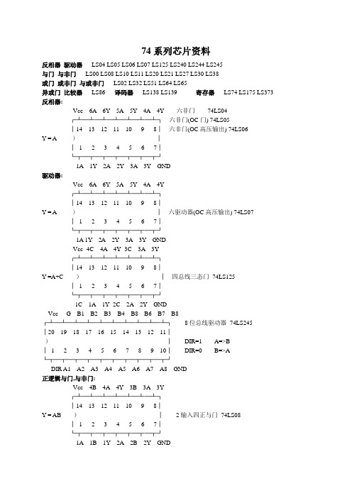
│14 13 12 11 10 9 8│
)
│ Y = A+B
│ 1 2 3 4 5 6 7│
└┬─┬─┬─┬─┬─┬─┬┘
1A 1B 1Y 2A 2B 2Y GND
Vcc 4Y 4B 4A 3Y 3B 3A
┌┴─┴─┴─┴─┴─┴─┴┐ 2 输入四或非门 74LS02
│14 13 12 11 10 9 8│
常见数字逻辑器件中文注解
74LS12 TTL 开路输出 3 输入端三与非门
74 系列:
74LS121 TTL 单稳态多谐振荡器
74LS00 TTL 2 输入端四与非门
74LS122 TTL 可再触发单稳态多谐振荡器
74LS01 TTL 集电极开路 2 输入端四与非门
74LS123 TTL 双可再触发单稳态多谐振荡器
└┬─┬─┬─┬─┬─┬─┬─┬┘
-1G 1A 1B -Y0 -Y1 -Y2 -Y3 GND
8*2 输入比较器 B8 A8 B7 A7 B6 A6 B5 A5
┌┴─┴─┴─┴─┴─┴─┴─┴─┴─┴┐ 8*2 输入比较器 74LS688
│20 19 18 17 16 15 14 13 12 11│
寄存器 LS74 LS175 LS373
反相器:
Vcc 6A 6Y 5A 5Y 4A 4Y 六非门 74LS04
┌┴─┴─┴─┴─┴─┴─┴┐ 六非门(OC 门) 74LS05
_ │14 13 12 11 10 9 8│ 六非门(OC 高压输出) 74LS06
Y=A )
│
│ 1 2 3 4 5 6 7│
3-8 译码器 74LS138
Vcc -Y0 -Y1 -Y2 -Y3 -Y4 -Y5 -Y6 __ _ _ _ __ _ _ __ _ _ __ _
常用74系列芯片功能速查
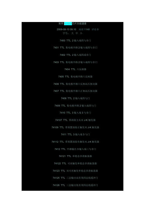
常用74系列芯片功能速查技术天地 2008-08-10 09:10 阅读1148 评论0字号:大中小7400 TTL 2输入端四与非门7401 TTL 集电极开路2输入端四与非门7402 TTL 2输入端四或非门7403 TTL 集电极开路2输入端四与非门7404 TTL 六反相器7405 TTL 集电极开路六反相器7406 TTL 集电极开路六反相高压驱动器7407 TTL 集电极开路六正相高压驱动器7408 TTL 2输入端四与门7409 TTL 集电极开路2输入端四与门7410 TTL 3输入端3与非门74107 TTL 带清除主从双J-K触发器74109 TTL 带预置清除正触发双J-K触发器7411 TTL 3输入端3与门74112 TTL 带预置清除负触发双J-K触发器7412 TTL 开路输出3输入端三与非门74121 TTL 单稳态多谐振荡器74122 TTL 可再触发单稳态多谐振荡器74123 TTL 双可再触发单稳态多谐振荡器74125 TTL 三态输出高有效四总线缓冲门74126 TTL 三态输出低有效四总线缓冲门7413 TTL 4输入端双与非施密特触发器74132 TTL 2输入端四与非施密特触发器74133 TTL 13输入端与非门74136 TTL 四异或门74138 TTL 3-8线译码器/复工器74139 TTL 双2-4线译码器/复工器7414 TTL 六反相施密特触发器74145 TTL BCD—十进制译码/驱动器7415 TTL 开路输出3输入端三与门74150 TTL 16选1数据选择/多路开关74151 TTL 8选1数据选择器74153 TTL 双4选1数据选择器74154 TTL 4线—16线译码器74155 TTL 图腾柱输出译码器/分配器74156 TTL 开路输出译码器/分配器74157 TTL 同相输出四2选1数据选择器74158 TTL 反相输出四2选1数据选择器7416 TTL 开路输出六反相缓冲/驱动器74160 TTL 可预置BCD异步清除计数器74161 TTL 可予制四位二进制异步清除计数器74162 TTL 可预置BCD同步清除计数器74163 TTL 可予制四位二进制同步清除计数器74164 TTL 八位串行入/并行输出移位寄存器74165 TTL 八位并行入/串行输出移位寄存器74166 TTL 八位并入/串出移位寄存器74169 TTL 二进制四位加/减同步计数器7417 TTL 开路输出六同相缓冲/驱动器74170 TTL 开路输出4×4寄存器堆74173 TTL 三态输出四位D型寄存器74174 TTL 带公共时钟和复位六D触发器74175 TTL 带公共时钟和复位四D触发器74180 TTL 9位奇数/偶数发生器/校验器74181 TTL 算术逻辑单元/函数发生器74185 TTL 二进制—BCD代码转换器74190 TTL BCD同步加/减计数器74191 TTL 二进制同步可逆计数器74192 TTL 可预置BCD双时钟可逆计数器74193 TTL 可预置四位二进制双时钟可逆计数器74194 TTL 四位双向通用移位寄存器74195 TTL 四位并行通道移位寄存器74196 TTL 十进制/二-十进制可预置计数锁存器74197 TTL 二进制可预置锁存器/计数器7420 TTL 4输入端双与非门7421 TTL 4输入端双与门7422 TTL 开路输出4输入端双与非门74221 TTL 双/单稳态多谐振荡器74240 TTL 八反相三态缓冲器/线驱动器74241 TTL 八同相三态缓冲器/线驱动器74243 TTL 四同相三态总线收发器74244 TTL 八同相三态缓冲器/线驱动器74245 TTL 八同相三态总线收发器74247 TTL BCD—7段15V输出译码/驱动器74248 TTL BCD—7段译码/升压输出驱动器74249 TTL BCD—7段译码/开路输出驱动器74251 TTL 三态输出8选1数据选择器/复工器74253 TTL 三态输出双4选1数据选择器/复工器74256 TTL 双四位可寻址锁存器74257 TTL 三态原码四2选1数据选择器/复工器74258 TTL 三态反码四2选1数据选择器/复工器74259 TTL 八位可寻址锁存器/3-8线译码器7426 TTL 2输入端高压接口四与非门74260 TTL 5输入端双或非门74266 TTL 2输入端四异或非门7427 TTL 3输入端三或非门74273 TTL 带公共时钟复位八D触发器74279 TTL 四图腾柱输出S-R锁存器7428 TTL 2输入端四或非门缓冲器74283 TTL 4位二进制全加器74290 TTL 二/五分频十进制计数器74293 TTL 二/八分频四位二进制计数器74295 TTL 四位双向通用移位寄存器74298 TTL 四2输入多路带存贮开关74299 TTL 三态输出八位通用移位寄存器7430 TTL 8输入端与非门7432 TTL 2输入端四或门74322 TTL 带符号扩展端八位移位寄存器74323 TTL 三态输出八位双向移位/存贮寄存器7433 TTL 开路输出2输入端四或非缓冲器74347 TTL BCD—7段译码器/驱动器74352 TTL 双4选1数据选择器/复工器74353 TTL 三态输出双4选1数据选择器/复工器74365 TTL 门使能输入三态输出六同相线驱动器74365 TTL 门使能输入三态输出六同相线驱动器74366 TTL 门使能输入三态输出六反相线驱动器74367 TTL 4/2线使能输入三态六同相线驱动器74368 TTL 4/2线使能输入三态六反相线驱动器7437 TTL 开路输出2输入端四与非缓冲器74373 TTL 三态同相八D锁存器74374 TTL 三态反相八D锁存器74375 TTL 4位双稳态锁存器74377 TTL 单边输出公共使能八D锁存器74378 TTL 单边输出公共使能六D锁存器74379 TTL 双边输出公共使能四D锁存器7438 TTL 开路输出2输入端四与非缓冲器74380 TTL 多功能八进制寄存器7439 TTL 开路输出2输入端四与非缓冲器74390 TTL 双十进制计数器74393 TTL 双四位二进制计数器7440 TTL 4输入端双与非缓冲器7442 TTL BCD—十进制代码转换器74352 TTL 双4选1数据选择器/复工器74353 TTL 三态输出双4选1数据选择器/复工器74365 TTL 门使能输入三态输出六同相线驱动器74366 TTL 门使能输入三态输出六反相线驱动器74367 TTL 4/2线使能输入三态六同相线驱动器74368 TTL 4/2线使能输入三态六反相线驱动器7437 TTL 开路输出2输入端四与非缓冲器74373 TTL 三态同相八D锁存器74374 TTL 三态反相八D锁存器74375 TTL 4位双稳态锁存器74377 TTL 单边输出公共使能八D锁存器74378 TTL 单边输出公共使能六D锁存器74379 TTL 双边输出公共使能四D锁存器7438 TTL 开路输出2输入端四与非缓冲器74380 TTL 多功能八进制寄存器7439 TTL 开路输出2输入端四与非缓冲器74390 TTL 双十进制计数器74393 TTL 双四位二进制计数器7440 TTL 4输入端双与非缓冲器7442 TTL BCD—十进制代码转换器74447 TTL BCD—7段译码器/驱动器7445 TTL BCD—十进制代码转换/驱动器74450 TTL 16:1多路转接复用器多工器74451 TTL 双8:1多路转接复用器多工器74453 TTL 四4:1多路转接复用器多工器7446 TTL BCD—7段低有效译码/驱动器74460 TTL 十位比较器74461 TTL 八进制计数器74465 TTL 三态同相2与使能端八总线缓冲器74466 TTL 三态反相2与使能八总线缓冲器74467 TTL 三态同相2使能端八总线缓冲器74468 TTL 三态反相2使能端八总线缓冲器74469 TTL 八位双向计数器7447 TTL BCD—7段高有效译码/驱动器7448 TTL BCD—7段译码器/内部上拉输出驱动74490 TTL 双十进制计数器74491 TTL 十位计数器74498 TTL 八进制移位寄存器7450 TTL 2-3/2-2输入端双与或非门74502 TTL 八位逐次逼近寄存器74503 TTL 八位逐次逼近寄存器7451 TTL 2-3/2-2输入端双与或非门74533 TTL 三态反相八D锁存器74534 TTL 三态反相八D锁存器7454 TTL 四路输入与或非门74540 TTL 八位三态反相输出总线缓冲器7455 TTL 4输入端二路输入与或非门74563 TTL 八位三态反相输出触发器74564 TTL 八位三态反相输出D触发器74573 TTL 八位三态输出触发器74574 TTL 八位三态输出D触发器74645 TTL 三态输出八同相总线传送接收器74670 TTL 三态输出4×4寄存器堆7473 TTL 带清除负触发双J-K触发器7474 TTL 带置位复位正触发双D触发器7476 TTL 带预置清除双J-K触发器7483 TTL 四位二进制快速进位全加器7485 TTL 四位数字比较器7486 TTL 2输入端四异或门7490 TTL 可二/五分频十进制计数器7493 TTL 可二/八分频二进制计数器7495 TTL 四位并行输入\输出移位寄存器7497 TTL 6位同步二进制乘法器常用74系列标准数字电路的中文名称资料器件代号器件名称74 74LS 74HC00 四2输入端与非门√ √ √01 四2输入端与非门(OC) √ √02 四2输入端或非门√ √ √03 四2输入端与非门(OC) √ √04 六反相器√ √ √05 六反相器(OC) √ √06 六高压输出反相器(OC,30V) √ √07 六高压输出缓冲,驱动器(OC,30V) √ √ √08 四2输入端与门√ √ √09 四2输入端与门(OC) √√ √10 三3输入端与非门√ √ √11 三3输入端与门√ √12 三3输入端与非门(OC) √ √ √13 双4输入端与非门√ √ √14 六反相器√ √ √15 三3输入端与门(OC) √ √16 六高压输出反相器(OC,15V) √17 六高压输出缓冲,驱动器(OC,15V) √20 双4输入端与非门√ √ √21 双4输入端与门√ √ √22 双4输入端与非门(OC) √ √25 双4输入端或非门(有选通端) √ √ √26 四2输入端高压输出与非缓冲器√ √ √27 三3输入端或非门√ √ √28 四2输入端或非缓冲器√ √ √30 8输入端与非门√ √ √32 四2输入端或门√ √ √33 四2输入端或非缓冲器(OC) √ √37 四2输入端与非缓冲器√ √38 四2输入端与非缓冲器(OC) √ √40 双4输入端与非缓冲器√ √ √42 4线-10线译码器(BCD输入) √ √43 4线-10线译码器(余3码输入) √44 4线-10线译码器(余3葛莱码输入) √48 4线-7段译码器√49 4线-7段译码器√50 双2路2-2输入与或非门√ √ √51 2路3-3输入,2路2-2输入与或非门√ √ √52 4路2-3-2-2输入与或门√53 4路2-2-2-2输入与或非门√54 4路2-3-3-2输入与或非门√ √55 2路4-4输入与或非门√60 双4输入与扩展器√ √61 三3输入与扩展器√62 4路2-3-3-2输入与或扩展器√64 4路4-2-3-2输入与或非门√65 4路4-2-3-2输入与或非门(OC) √70 与门输入J-K触发器√71 与或门输入J-K触发器√72 与门输入J-K触发器√74 双上升沿D型触发器√ √78 双D型触发器√ √85 四位数值比较器√86 四2输入端异或门√ √ √87 4位二进制原码/反码√95 4位移位寄存器√101 与或门输入J-K触发器√102 与门输入J-K触发器√107 双主-从J-K触发器√108 双主-从J-K触发器√109 双主-从J-K触发器√110 与门输入J-K触发器√111 双主-从J-K触发器√ √112 双下降沿J-K触发器√113 双下降沿J-K触发器√114 双下降沿J-K触发器√116 双4位锁存器√120 双脉冲同步驱动器√121 单稳态触发器√ √ √122 可重触发单稳态触发器√ √ √123 可重触发双稳态触发器√ √ √125 四总线缓冲器√ √ √126 四总线缓冲器√ √ √128 四2输入端或非线驱动器√ √ √132 四2输入端与非门√ √ √。
74ACTQ374SC资料
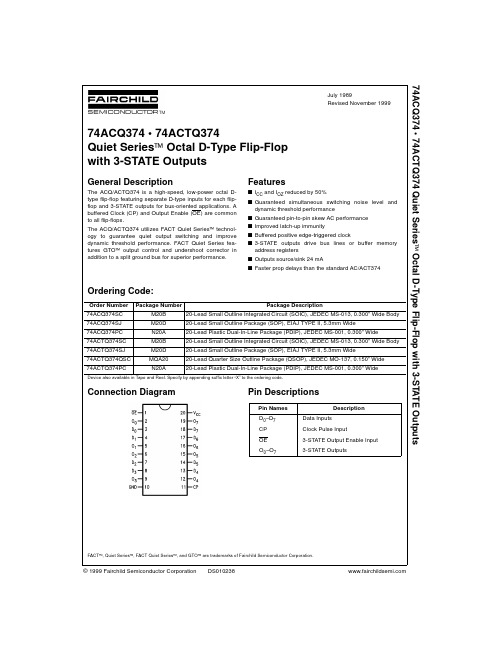
Device also available in Tape and Reel. Specify by appending suffix letter “X” to the ordering am
Pin Descriptions
Pin Names D0 – D7 CP OE O0–O7 Data Inputs Clock Pulse Input 3-STATE Output Enable Input 3-STATE Outputs Description
Features
s ICC and IOZ reduced by 50% s Guaranteed simultaneous switching noise level and dynamic threshold performance s Guaranteed pin-to-pin skew AC performance s Improved latch-up immunity s Buffered positive edge-triggered clock s 3-STATE outputs drive bus lines or buffer memory address registers s Outputs source/sink 24 mA s Faster prop delays than the standard AC/ACT374
元器件交易网
74ACQ374 • 74ACTQ374
Logic Symbols
Functional Description
The ACQ/ACTQ374 consists of eight edge-triggered flipflops with individual D-type inputs and 3-STATE true outputs. The buffered clock and buffered Output Enable are common to all flip-flops. The eight flip-flops will store the state of their individual D-type inputs that meet the setup and hold time requirements on the LOW-to-HIGH Clock (CP) transition. With the Output Enable (OE) LOW, the contents of the eight flip-flops are available at the outputs. When the OE is HIGH, the outputs go to the high impedance state. Operation of the OE input does not affect the state of the flip-flops.
常用74系列芯片功能速查表

常用74系列标准数字电路的中文名称资料器件代号器件名称74 74LS 74HC00 四2输入端与非门√ √ √01 四2输入端与非门(OC) √ √02 四2输入端或非门√ √ √03 四2输入端与非门(OC) √ √04 六反相器√ √ √05 六反相器(OC) √ √06 六高压输出反相器(OC,30V) √ √07 六高压输出缓冲,驱动器(OC,30V) √ √ √08 四2输入端与门√ √ √09 四2输入端与门(OC) √ √ √10 三3输入端与非门√ √√11 三3输入端与门√ √12 三3输入端与非门(OC) √ √ √13 双4输入端与非门√ √ √14 六反相器√ √ √15 三3输入端与门(OC) √ √16 六高压输出反相器(OC,15V) √17 六高压输出缓冲,驱动器(OC,15V) √20 双4输入端与非门√ √ √21 双4输入端与门√ √ √22 双4输入端与非门(OC) √ √25 双4输入端或非门(有选通端) √ √ √26 四2输入端高压输出与非缓冲器√ √ √27 三3输入端或非门√ √ √28 四2输入端或非缓冲器√ √ √30 8输入端与非门√ √ √32 四2输入端或门√ √ √33 四2输入端或非缓冲器(OC) √ √37 四2输入端与非缓冲器√ √38 四2输入端与非缓冲器(OC) √ √40 双4输入端与非缓冲器√ √ √42 4线-10线译码器(BCD输入) √ √43 4线-10线译码器(余3码输入) √44 4线-10线译码器(余3葛莱码输入) √48 4线-7段译码器√49 4线-7段译码器√50 双2路2-2输入与或非门√ √ √51 2路3-3输入,2路2-2输入与或非门√ √ √52 4路2-3-2-2输入与或门√53 4路2-2-2-2输入与或非门√54 4路2-3-3-2输入与或非门√ √55 2路4-4输入与或非门√60 双4输入与扩展器√ √61 三3输入与扩展器√62 4路2-3-3-2输入与或扩展器√64 4路4-2-3-2输入与或非门√65 4路4-2-3-2输入与或非门(OC) √70 与门输入J-K触发器√71 与或门输入J-K触发器√72 与门输入J-K触发器√74 双上升沿D型触发器√ √78 双D型触发器√ √85 四位数值比较器√86 四2输入端异或门√ √ √87 4位二进制原码/反码√95 4位移位寄存器√101 与或门输入J-K触发器√102 与门输入J-K触发器√107 双主-从J-K触发器√108 双主-从J-K触发器√109 双主-从J-K触发器√110 与门输入J-K触发器√111 双主-从J-K触发器√ √112 双下降沿J-K触发器√113 双下降沿J-K触发器√114 双下降沿J-K触发器√116 双4位锁存器√120 双脉冲同步驱动器√121 单稳态触发器√ √ √122 可重触发单稳态触发器√ √ √123 可重触发双稳态触发器√ √ √125 四总线缓冲器√ √ √126 四总线缓冲器√ √ √128 四2输入端或非线驱动器√ √ √132 四2输入端与非门√ √ √常用74系列芯片功能速查发表于2007/8/27 9:31:267400 TTL 2输入端四与非门7401 TTL 2输入端四与非门7402 TTL 2输入端四或非门7403 TTL 2输入端四与非门7404 TTL 六反相器7405 TTL六反相器7406 TTL六反相高压驱动器7407 TTL六正相高压驱动器7408 TTL 2输入端四与门7409 TTL 2输入端四与门7410 TTL 3输入端3与非门74107 TTL 带清除主从双J-K触发器74109 TTL 带预置清除正触发双J-K触发器7411 TTL 3输入端3与门74112 TTL 带预置清除负触发双J-K触发器7412 TTL 开路输出3输入端三与非门74121 TTL 单稳态多谐振荡器74122 TTL 可再触发单稳态多谐振荡器74123 TTL 双可再触发单稳态多谐振荡器74125 TTL 三态输出高有效四总线缓冲门74126 TTL 三态输出低有效四总线缓冲门7413 TTL 4输入端双与非施密特触发器74132 TTL 2输入端四与非施密特触发器74133 TTL 13输入端与非门74136 TTL 四异或门74138 TTL 3-8线译码器/复工器74139 TTL 双2-4线译码器/复工器7414 TTL 六反相施密特触发器74145 TTL BCD—十进制译码/驱动器7415 TTL 开路输出3输入端三与门74150 TTL 16选1数据选择/多路开关74151 TTL 8选1数据选择器74153 TTL 双4选1数据选择器74154 TTL 4线—16线译码器74155 TTL 图腾柱输出译码器/分配器74156 TTL 开路输出译码器/分配器74157 TTL 同相输出四2选1数据选择器74158 TTL 反相输出四2选1数据选择器7416 TTL 开路输出六反相缓冲/驱动器74160 TTL 可预置BCD异步清除计数器74161 TTL 可予制四位二进制异步清除计数器74162 TTL 可预置BCD同步清除计数器74163 TTL 可予制四位二进制同步清除计数器74164 TTL 八位串行入/并行输出移位寄存器74165 TTL 八位并行入/串行输出移位寄存器74166 TTL 八位并入/串出移位寄存器74169 TTL 二进制四位加/减同步计数器7417 TTL 开路输出六同相缓冲/驱动器74170 TTL 开路输出4×4寄存器堆74173 TTL 三态输出四位D型寄存器74174 TTL 带公共时钟和复位六D触发器74175 TTL 带公共时钟和复位四D触发器74180 TTL 9位奇数/偶数发生器/校验器74181 TTL 算术逻辑单元/函数发生器74185 TTL 二进制—BCD代码转换器74190 TTL BCD同步加/减计数器74191 TTL 二进制同步可逆计数器74192 TTL 可预置BCD双时钟可逆计数器74193 TTL 可预置四位二进制双时钟可逆计数器74194 TTL 四位双向通用移位寄存器74195 TTL 四位并行通道移位寄存器74196 TTL 十进制/二-十进制可预置计数锁存器74197 TTL 二进制可预置锁存器/计数器7420 TTL 4输入端双与非门7421 TTL 4输入端双与门7422 TTL 开路输出4输入端双与非门74221 TTL 双/单稳态多谐振荡器74240 TTL 八反相三态缓冲器/线驱动器74241 TTL 八同相三态缓冲器/线驱动器74243 TTL 四同相三态总线收发器74244 TTL 八同相三态缓冲器/线驱动器74245 TTL 八同相三态总线收发器74247 TTL BCD—7段15V输出译码/驱动器74248 TTL BCD—7段译码/升压输出驱动器74249 TTL BCD—7段译码/开路输出驱动器74251 TTL 三态输出8选1数据选择器/复工器74253 TTL 三态输出双4选1数据选择器/复工器74256 TTL 双四位可寻址锁存器74257 TTL 三态原码四2选1数据选择器/复工器74258 TTL 三态反码四2选1数据选择器/复工器74259 TTL 八位可寻址锁存器/3-8线译码器7426 TTL 2输入端高压接口四与非门74260 TTL 5输入端双或非门74266 TTL 2输入端四异或非门7427 TTL 3输入端三或非门74273 TTL 带公共时钟复位八D触发器74279 TTL 四图腾柱输出S-R锁存器7428 TTL 2输入端四或非门缓冲器74283 TTL 4位二进制全加器74290 TTL 二/五分频十进制计数器74293 TTL 二/八分频四位二进制计数器74295 TTL 四位双向通用移位寄存器74298 TTL 四2输入多路带存贮开关74299 TTL 三态输出八位通用移位寄存器7430 TTL 8输入端与非门7432 TTL 2输入端四或门74322 TTL 带符号扩展端八位移位寄存器74323 TTL 三态输出八位双向移位/存贮寄存器7433 TTL 开路输出2输入端四或非缓冲器74347 TTL BCD—7段译码器/驱动器74352 TTL 双4选1数据选择器/复工器74353 TTL 三态输出双4选1数据选择器/复工器74365 TTL 门使能输入三态输出六同相线驱动器74365 TTL 门使能输入三态输出六同相线驱动器74366 TTL 门使能输入三态输出六反相线驱动器74367 TTL 4/2线使能输入三态六同相线驱动器74368 TTL 4/2线使能输入三态六反相线驱动器7437 TTL 开路输出2输入端四与非缓冲器74373 TTL 三态同相八D锁存器74374 TTL 三态反相八D锁存器74375 TTL 4位双稳态锁存器74377 TTL 单边输出公共使能八D锁存器74378 TTL 单边输出公共使能六D锁存器74379 TTL 双边输出公共使能四D锁存器7438 TTL 开路输出2输入端四与非缓冲器74380 TTL 多功能八进制寄存器7439 TTL 开路输出2输入端四与非缓冲器74390 TTL 双十进制计数器74393 TTL 双四位二进制计数器7440 TTL 4输入端双与非缓冲器7442 TTL BCD—十进制代码转换器74352 TTL 双4选1数据选择器/复工器74353 TTL 三态输出双4选1数据选择器/复工器74365 TTL 门使能输入三态输出六同相线驱动器74366 TTL 门使能输入三态输出六反相线驱动器74367 TTL 4/2线使能输入三态六同相线驱动器74368 TTL 4/2线使能输入三态六反相线驱动器7437 TTL 开路输出2输入端四与非缓冲器74373 TTL 三态同相八D锁存器74374 TTL 三态反相八D锁存器74375 TTL 4位双稳态锁存器74377 TTL 单边输出公共使能八D锁存器74378 TTL 单边输出公共使能六D锁存器74379 TTL 双边输出公共使能四D锁存器7438 TTL 开路输出2输入端四与非缓冲器74380 TTL 多功能八进制寄存器7439 TTL 开路输出2输入端四与非缓冲器74390 TTL 双十进制计数器74393 TTL 双四位二进制计数器7440 TTL 4输入端双与非缓冲器7442 TTL BCD—十进制代码转换器74447 TTL BCD—7段译码器/驱动器7445 TTL BCD—十进制代码转换/驱动器74450 TTL 16:1多路转接复用器多工器74451 TTL 双8:1多路转接复用器多工器74453 TTL 四4:1多路转接复用器多工器7446 TTL BCD—7段低有效译码/驱动器74460 TTL 十位比较器74461 TTL 八进制计数器74465 TTL 三态同相2与使能端八总线缓冲器74466 TTL 三态反相2与使能八总线缓冲器74467 TTL 三态同相2使能端八总线缓冲器74468 TTL 三态反相2使能端八总线缓冲器74469 TTL 八位双向计数器7447 TTL BCD—7段高有效译码/驱动器7448 TTL BCD—7段译码器/内部上拉输出驱动74490 TTL 双十进制计数器74491 TTL 十位计数器74498 TTL 八进制移位寄存器7450 TTL 2-3/2-2输入端双与或非门74502 TTL 八位逐次逼近寄存器74503 TTL 八位逐次逼近寄存器7451 TTL 2-3/2-2输入端双与或非门74533 TTL 三态反相八D锁存器74534 TTL 三态反相八D锁存器7454 TTL 四路输入与或非门74540 TTL 八位三态反相输出总线缓冲器7455 TTL 4输入端二路输入与或非门74563 TTL 八位三态反相输出触发器74564 TTL 八位三态反相输出D触发器74573 TTL 八位三态输出触发器74574 TTL 八位三态输出D触发器74645 TTL 三态输出八同相总线传送接收器74670 TTL 三态输出4×4寄存器堆7473 TTL 带清除负触发双J-K触发器7474 TTL 带置位复位正触发双D触发器7476 TTL 带预置清除双J-K触发器7483 TTL 四位二进制快速进位全加器7485 TTL 四位数字比较器7486 TTL 2输入端四异或门7490 TTL 可二/五分频十进制计数器7493 TTL 可二/八分频二进制计数器7495 TTL 四位并行输入\输出移位寄存器7497 TTL 6位同步二进制乘法器。
74ACTQ273资料

元器件交易网
74ACTQ273
Logic Symbols
IEEE/IEC
Mode Select-Function Table
Inputs Operating Mode MR Reset (Clear) Load “1” Load “0”
H = HIGH Voltage Level L = LOW Voltage Level X = Immaterial = LOW-to-HIGH Transition
Recommended Operating Conditions
Supply Voltage (VCC) Input Voltage (VI) Output Voltage (VO) Operating Temperature (TA) Minimum Input Edge Rate ∆V/∆t VIN from 0.8V to 2.0V VCC @ 4.5V, 5.5V 125 mV/ns 4.5V to 5.5V 0V to VCC 0V to VCC −40°C to +85°C
Ordering Code:
Order Number 74ACTQ273SC 74ACTQ273SJ 74ACTQ273MTC 74ACTQ273PC Package Number M20B M20D MTC20 N20A Package Description 20-Lead Small Outline Integrated Circuit, JEDEC MS-013, 0.300” Wide Body 20-Lead Small Outline Package, EIAJ TYPE II, 5.3mm Wide 20-Lead Thin Shrink Small Outline Package (TSSOP), JEDEC MO-153, 4.4mm Wide 20-Lead Plastic Dual-In-Line Package, JEDEC MS-001, 0.300” Wide
HD74ACT245中文资料
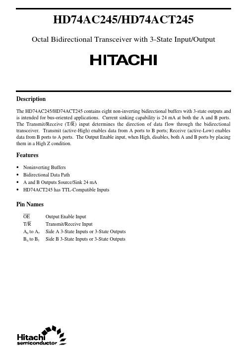
HD74AC245/HD74ACT245 Octal Bidirectional Transceiver with 3-State Input/OutputDescriptionThe HD74AC245/HD74ACT245 contains eight non-inverting bidirectional buffers with 3-state outputs and is intended for bus-oriented applications. Current sinking capability is 24 mA at both the A and B ports. The Transmit/Receive (T/R) input determines the direction of data flow through the bidirectional transceiver. Transmit (active-High) enables data from A ports to B ports; Receive (active-Low) enables data from B ports to A ports. The Output Enable input, when High, disables, both A and B ports by placing them in a High Z condition.Features• Noninverting Buffers• Bidirectional Data Path• A and B Outputs Source/Sink 24 mA• HD74ACT245 has TTL-Compatible InputsPin NamesOE Output Enable InputT/R Transmit/Receive InputA0 to A7Side A 3-State Inputs or 3-State OutputsB0 to B7Side B 3-State Inputs or 3-State OutputsHD74AC245/HD74ACT245Pin ArrangementTruth TablesInputsOE T/R OutputsL L Bus B Data to Bus A L H Bus A Data to Bus B H X High Z StateH:High Voltage LevelL:Low Voltage LevelX:Immaterial2HD74AC245/HD74ACT2453DC Characteristics (unless otherwise specified)ItemSymbol Max Unit ConditionMaximum quiescent supply current I CC 80µA V IN = V CC or ground, V CC = 5.5 V,Ta = Worst caseMaximum quiescent supply current I CC 8.0µA V IN = V CC or ground, V CC = 5.5 V,Ta = 25°CMaximum additional I CC /input (HD74ACT245)I CCT1.5mAV IN = V CC – 2.1 V, V CC = 5.5 V,Ta = Worst caseAC Characteristics: HD74AC245Ta = +25°C C L = 50 pFTa = –40°C to +85°C C L = 50 pF ItemSymbol V CC (V)*1Min Typ Max Min Max Unit Propagation delay t PLH3.3 1.0 5.08.5 1.09.0nsData to output 5.0 1.0 3.5 6.5 1.07.0Propagation delay t PHL 3.3 1.0 5.08.5 1.09.0ns Data to output 5.0 1.0 3.5 6.0 1.07.0Output enable time t PZH 3.3 1.07.011.5 1.012.5ns 5.0 1.0 5.08.5 1.09.0Output enable time t PZL 3.3 1.07.512.0 1.013.5ns 5.0 1.0 5.59.0 1.09.5Output disable time t PHZ 3.3 1.0 6.512.0 1.012.5ns 5.0 1.0 5.59.0 1.010.0Output disable time t PLZ 3.3 1.07.011.5 1.013.0ns 5.01.05.59.01.010.0Note:1.Voltage Range 3.3 is 3.3 V ± 0.3 VVoltage Range 5.0 is 5.0 V ± 0.5 VHD74AC245/HD74ACT2454AC Characteristics: HD74ACT245Ta = +25°C C L = 50 pFTa = –40°C to +85°C C L = 50 pF ItemSymbol V CC (V)*1Min Typ Max Min Max Unit Propagation delay Data to output t PLH 5.0 1.0 4.07.5 1.08.0ns Propagation delay Data to output t PHL 5.0 1.0 4.08.0 1.09.0ns Output enable time t PZH 5.0 1.0 5.010.0 1.011.0ns Output enable time t PZL 5.0 1.0 5.510.0 1.012.0ns Output disable time t PHZ 5.0 1.0 5.510.0 1.011.0ns Output disable time t PLZ5.01.05.010.01.011.0nsNote:1.Voltage Range 5.0 is 5.0 V ± 0.5 VCapacitanceItemSymbol Typ Unit Condition Input capacitance C IN 4.5pF V CC = 5.5 V Input/output capacitance C I/O 15.0pF V CC = 5.5 V Power dissipation capacitanceC PD45.0pFV CC = 5.0 VHitachi Code JEDEC EIAJWeight (reference value)DP-20N —Conforms 1.26 gUnit: mm元器件交易网Hitachi Code JEDEC EIAJWeight (reference value)TTP-20DA ——0.07 gUnit: mm*Dimension including the plating thicknessBase material dimension元器件交易网Cautions1.Hitachi neither warrants nor grants licenses of any rights of Hitachi’s or any third party’s patent,copyright, trademark, or other intellectual property rights for information contained in this document.Hitachi bears no responsibility for problems that may arise with third party’s rights, includingintellectual property rights, in connection with use of the information contained in this document.2.Products and product specifications may be subject to change without notice. Confirm that you have received the latest product standards or specifications before final design, purchase or use.3.Hitachi makes every attempt to ensure that its products are of high quality and reliability. However,contact Hitachi’s sales office before using the product in an application that demands especially high quality and reliability or where its failure or malfunction may directly threaten human life or cause risk of bodily injury, such as aerospace, aeronautics, nuclear power, combustion control, transportation,traffic, safety equipment or medical equipment for life support.4.Design your application so that the product is used within the ranges guaranteed by Hitachi particularly for maximum rating, operating supply voltage range, heat radiation characteristics, installationconditions and other characteristics. Hitachi bears no responsibility for failure or damage when used beyond the guaranteed ranges. Even within the guaranteed ranges, consider normally foreseeable failure rates or failure modes in semiconductor devices and employ systemic measures such as fail-safes, so that the equipment incorporating Hitachi product does not cause bodily injury, fire or other consequential damage due to operation of the Hitachi product.5.This product is not designed to be radiation resistant.6.No one is permitted to reproduce or duplicate, in any form, the whole or part of this document without written approval from Hitachi.7.Contact Hitachi’s sales office for any questions regarding this document or Hitachi semiconductor products.Hitachi, Ltd.Semiconductor & Integrated Circuits.Nippon Bldg., 2-6-2, Ohte-machi, Chiyoda-ku, Tokyo 100-0004, Japan Tel: Tokyo (03) 3270-2111 Fax: (03) 3270-5109Copyright ' Hitachi, Ltd., 1999. All rights reserved. Printed in Japan.Hitachi Asia Pte. Ltd.16 Collyer Quay #20-00Hitachi TowerSingapore 049318Tel: 535-2100Fax: 535-1533URLNorthAmerica : http:/Europe : /hel/ecg Asia (Singapore): .sg/grp3/sicd/index.htm Asia (Taiwan): /E/Product/SICD_Frame.htm Asia (HongKong): /eng/bo/grp3/index.htm Japan : http://www.hitachi.co.jp/Sicd/indx.htmHitachi Asia Ltd.Taipei Branch Office3F, Hung Kuo Building. No.167, Tun-Hwa North Road, Taipei (105)Tel: <886> (2) 2718-3666Fax: <886> (2) 2718-8180Hitachi Asia (Hong Kong) Ltd.Group III (Electronic Components)7/F., North Tower, World Finance Centre,Harbour City, Canton Road, Tsim Sha Tsui,Kowloon, Hong Kong Tel: <852> (2) 735 9218Fax: <852> (2) 730 0281 Telex: 40815 HITEC HXHitachi Europe Ltd.Electronic Components Group.Whitebrook ParkLower Cookham Road MaidenheadBerkshire SL6 8YA, United Kingdom Tel: <44> (1628) 585000Fax: <44> (1628) 778322Hitachi Europe GmbHElectronic components Group Dornacher Stra§e 3D-85622 Feldkirchen, Munich GermanyTel: <49> (89) 9 9180-0Fax: <49> (89) 9 29 30 00Hitachi Semiconductor (America) Inc.179 East Tasman Drive,San Jose,CA 95134 Tel: <1> (408) 433-1990Fax: <1>(408) 433-0223For further information write to:。
MC74ACT564中文资料
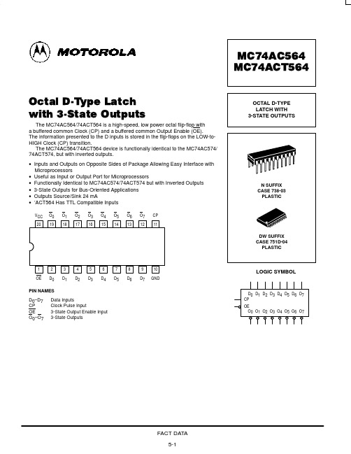
VIL
Maximum Low Level Input Voltage
V
VOH
Minimum High Level Output Voltage
V
V
µA
5.5 5.5 5.5 5.5
Hale Waihona Puke ±0.5±5.0 75 –75
µA mA mA µA
IOLD IOHD ICC
8.0
80
* All outputs loaded; thresholds on input associated with output under test. † Maximum test duration 2.0 ms, one output loaded at a time. Note: IIN and ICC @ 3.0 V are guaranteed to be less than or equal to the respective limit @ 5.5 V VCC.
RECOMMENDED OPERATING CONDITIONS
Symbol VCC Vin, Vout Supply Voltage DC Input Voltage, Output Voltage (Ref. to GND) VCC @ 3.0 V tr, tf Input Rise and Fall Time (Note 1) ′AC Devices except Schmitt Inputs VCC @ 4.5 V VCC @ 5.5 V tr, tf TJ TA IOH IOL Input Rise and Fall Time (Note 2) ′ACT Devices except Schmitt Inputs Junction Temperature (PDIP) Operating Ambient Temperature Range Output Current — High Output Current — Low –40 25 VCC @ 4.5 V VCC @ 5.5 V Parameter ′AC ′ACT Min 2.0 4.5 0 150 40 25 10 ns/V 8.0 140 85 –24 24 °C °C mA mA ns/V Typ 5.0 5.0 Max 6.0 5.5 VCC V Unit V
74ACT11874DW资料

元器件交易网IMPORTANT NOTICETexas Instruments and its subsidiaries (TI) reserve the right to make changes to their products or to discontinueany product or service without notice, and advise customers to obtain the latest version of relevant informationto verify, before placing orders, that information being relied on is current and complete. All products are soldsubject to the terms and conditions of sale supplied at the time of order acknowledgement, including thosepertaining to warranty, patent infringement, and limitation of liability.TI warrants performance of its semiconductor products to the specifications applicable at the time of sale inaccordance with TI’s standard warranty. Testing and other quality control techniques are utilized to the extentTI deems necessary to support this warranty. Specific testing of all parameters of each device is not necessarilyperformed, except those mandated by government requirements.CERTAIN APPLICATIONS USING SEMICONDUCTOR PRODUCTS MAY INVOLVE POTENTIAL RISKS OFDEATH, PERSONAL INJURY, OR SEVERE PROPERTY OR ENVIRONMENTAL DAMAGE (“CRITICALAPPLICATIONS”). TI SEMICONDUCTOR PRODUCTS ARE NOT DESIGNED, AUTHORIZED, ORWARRANTED TO BE SUITABLE FOR USE IN LIFE-SUPPORT DEVICES OR SYSTEMS OR OTHERCRITICAL APPLICATIONS. INCLUSION OF TI PRODUCTS IN SUCH APPLICATIONS IS UNDERSTOOD TOBE FULLY AT THE CUSTOMER’S RISK.In order to minimize risks associated with the customer’s applications, adequate design and operatingsafeguards must be provided by the customer to minimize inherent or procedural hazards.TI assumes no liability for applications assistance or customer product design. TI does not warrant or representthat any license, either express or implied, is granted under any patent right, copyright, mask work right, or otherintellectual property right of TI covering or relating to any combination, machine, or process in which suchsemiconductor products or services might be or are used. TI’s publication of information regarding any thirdparty’s products or services does not constitute TI’s approval, warranty or endorsement thereof.Copyright © 1998, Texas Instruments Incorporated。
- 1、下载文档前请自行甄别文档内容的完整性,平台不提供额外的编辑、内容补充、找答案等附加服务。
- 2、"仅部分预览"的文档,不可在线预览部分如存在完整性等问题,可反馈申请退款(可完整预览的文档不适用该条件!)。
- 3、如文档侵犯您的权益,请联系客服反馈,我们会尽快为您处理(人工客服工作时间:9:00-18:30)。
TECHNICAL DATAKK 74ACT534Octal 3-StateInverting D Flip-FlopHigh-Speed Silicon-Gate CMOSThe KK HC/HCT534. The KK 74ACT534 may be used as a level converter for interfacing TTL or NMOS outputs to High Speed CMOS inputs.Data meeting the setup time is clocked, in inverted form, to the outputs with the rising edge of the Clock. The Output Enable input does not affect the states of the flip-flops, but when Output Enable is high, the outputs are forced to the high impedance state. Thus, data may be stored even when the outputs are not enabled. • TTL/NMOS Compatible Input Levels• Outputs Directly Interface to CMOS, NMOS, and TTL • Operating Voltage Range: 4.5 to 5.5 V• Low Input Current: 1.0 µA; 0.1 µA @ 25°C • Outputs Source/Sink 24 mALOGIC DIAGRAMPIN 20=V CC PIN 10 = GNDFUNCTION TABLEX = don’t careZ = high impedancePIN ASSIGNMENTMAXIMUM RATINGS*Symbol Parameter ValueUnit V CC DC Supply Voltage (Referenced to GND) -0.5 to +7.0 VV IN DC Input Voltage (Referenced to GND) -0.5 to V CC +0.5 VV OUT DC Output Voltage (Referenced to GND) -0.5 to V CC +0.5 VI IN DC Input Current, per Pin ±20 mAI OUT DC Output Sink/Source Current, per Pin ±50 mAI CC DC Supply Current, V CC and GND Pins ±50 mAP D Power Dissipation in Still Air, Plastic DIP+ SOIC Package+ 750500mWTstg Storage Temperature -65 to +150 °CT L Lead Temperature, 1 mm from Case for 10 Seconds(Plastic DIP or SOIC Package)260 °C*Maximum Ratings are those values beyond which damage to the device may occur.Functional operation should be restricted to the Recommended Operating Conditions.+Derating - Plastic DIP: - 10 mW/°C from 65° to 125°CSOIC Package: : - 7 mW/°C from 65° to 125°CRECOMMENDED OPERATING CONDITIONSSymbol Parameter MinMaxUnit V CC DC Supply Voltage (Referenced to GND) 4.5 5.5 VV IN, V OUT DC Input Voltage, Output Voltage (Referenced to GND) 0 V CC VT J Junction Temperature (PDIP) 140 °CT A Operating Temperature, All Package Types -40 +85 °CI OH Output Current - High -24 mAI OL Output Current - Low 24 mAt r, t f Input Rise and Fall Time *(except Schmitt Inputs) V CC =4.5 VV CC =5.5 V108.0ns/V* VINfrom 0.8 V to 2.0 VThis device contains protection circuitry to guard against damage due to high static voltages or electric fields. However, precautions must be taken to avoid applications of any voltage higher than maximum rated voltages to this high-impedance circuit. For proper operation, V IN and V OUT should be constrained to the range GND≤(V IN or V OUT)≤V CC.Unused inputs must always be tied to an appropriate logic voltage level (e.g., either GND or V CC). Unused outputs must be left open.DC ELECTRICAL CHARACTERISTICS (Voltages Referenced to GND)V CC Guaranteed Limits Symbol Parameter TestConditions V25 °C -40°C to85°CUnitV IH Minimum High-Level Input Voltage V OUT= 0.1 V or V CC-0.1 V 4.55.52.02.02.02.0VV IL Maximum Low -Level Input Voltage V OUT= 0.1 V or V CC-0.1 V 4.55.50.80.80.80.8VV OH Minimum High-Level Output Voltage I OUT≤ -50 µA 4.55.54.45.44.45.4V*VIN=V IH or V ILI OH=-24 mAI OH=-24 mA4.55.53.864.863.764.76V OL Maximum Low-Level Output Voltage I OUT≤ 50 µA 4.55.50.10.10.10.1V*VIN= V IH or V ILI OL=24 mAI OL=24 mA4.55.50.360.360.440.44I IN Maximum InputLeakage CurrentV IN=V CC or GND 5.5±0.1 ±1.0 µA∆I CCT Additional Max.I CC/InputV IN=V CC - 2.1 V 5.5 1.5 mAI OZ Maximum Three-State LeakageCurrent V IN (OE)= V IH or V ILV IN =V CC or GNDV OUT =V CC or GND5.5±0.5 ±5.0 µAI OLD+Minimum DynamicOutput CurrentV OLD=1.65 V Max 5.575 mAI OHD+Minimum DynamicOutput CurrentV OHD=3.85 V Min 5.5-75 mAI CC Maximum QuiescentSupply Current(per Package)V IN=V CC or GND 5.58.0 80 µA* All outputs loaded; thresholds on input associated with output under test.+Maximum test duration 2.0 ms, one output loaded at a time.AC ELECTRICAL CHARACTERISTICS (V CC=5.0 V ± 10%, C L=50pF,Input t r=t f=3.0 ns)GuaranteedLimits Symbol Parameter 25 °C -40°C to 85°C UnitMin Max Min Maxf max Maximum Clock Frequency (Figure 1) 120 nst PLH Propagation Delay, Clock to Q (Figure 1) 2.5 11.5 2.0 12.5 nst PHL Propagation Delay, Clock to Q (Figure 1) 2.0 10.5 2.0 12.0 nst PZH Propagation Delay, Output Enable to Q(Figure 2)2.5 12.0 2.0 12.5 nst PZL Propagation Delay, Output Enable to Q(Figure 2)2.0 11.0 2.0 11.5 nst PHZ Propagation Delay, Output Enable to Q(Figure 2)1.5 12.5 1.0 13.5 nst PLZ Propagation Delay, Output Enable to Q(Figure 2)1.5 10.5 1.0 10.5 nsC IN Maximum Input Capacitance 4.5 4.5 pFTypical @25°C,V CC=5.0 VC PD Power Dissipation Capacitance 40 pFTIMING REQUIREMENTS (V CC=5.0 V ± 10%, C L=50pF, Input t r=t f=3.0 ns)GuaranteedLimits Symbol Parameter 25 °C -40°C to85°CUnitt su Minimum Setup Time, Data to Clock (Figure 3) 3.5 4.0nst h Minimum Hold Time, Clock to Data (Figure 3) 1.0 1.5nst w Minimum Pulse Width, Clock (Figure 1) 3.5 3.5 nsFigure 1. Switching Waveforms Figure 2. Switching WaveformsFigure 3. Switching WaveformsEXPANDED LOGIC DIAGRAM。
