RClamp0504S.TCT中文资料
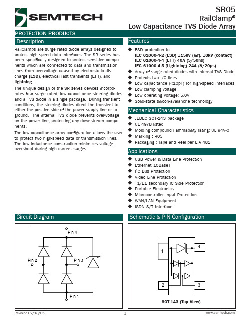
SR05.TCT中文资料
Forward Voltage vs. Forward Current
10 9
% Change in Capacitance 0 -2 -4 -6 -8 -10 -12 -14 -16
Capacitance vs. Reverse Voltage
Forward Voltage - V F (V)
8 7 6 5 4 3 2 1 0 0 5 10 15 20 25 30 35 40 45 50 Forward Current - IF (A) Waveform Parameters: tr = 8µs td = 20µs
SR05
Mechanical Characteristics
JEDEC SOT-143 package UL 497B listed Molding compound flammability rating: UL 94V-0 Marking : R05 Packaging : Tape and Reel per EIA 481
0
25
50
75
100
125
150
Ambient Temperature - TA (oC)
Pulse Waveform
110 100 90 80 Percent of IPP 70 60 50 40 30 20 10 0 0 5 10 15 Time (µs) 20 25 30 td = IPP/2 e
10 Peak Pulse Power - PPk (kW)
Power Derating Curve
1IP 90 80 70 60 50 40 30 20 10 0
1
0.1
RCLAMP0821P中文资料

SLP1006P2 package Molding compound flammability rating: UL 94V-0 Marking: Marking code Packaging : Tape and Reel Lead Finish: NiPdAu RoHS/WEEE Compliant
I/O Line
RClamp0821P
RClamp0821P Spice Model
Table 1 - RClamp0821P Spice Parameters
Parameter
Unit
D1 (LCRD) D2 (LCRD)
IS
Amp
1.0E-20
1.0E-20
BV
Vlt
0.7
元器件交易网
PROTECTION PRODUCTS Applications Information
Device Connection Options
These low capacitance TVS diodes are designed to provide common mode protection for one high-speed line or differential protection for one line pair. The device is bidirectional and may be used on lines where the signal polarity is positive and negative.
1.8 GHz
1
2 34
3: .00910 dB 2.5 GHz
4: -.11980 dB 2.7 GHz
HMBT8050中文资料

HMBT8050中文资料Page No. : 1/3HMBT8050NPN EPITAXIAL TRANSISTORDescriptionThe HMBT8050 is designed for general purpose amplifier applications.FeaturesHigh DC Current hFE=150-400 at IC=150mA ? Complementary to HMBT8550Absolute Maximum RatingsMaximum TemperaturesStorage Temperature........................................................................................... -55 ~ +150 °C Junction Temperature.................................................................................... +150 °C Maximum ? Maximum Power DissipationTotal Power Dissipation (Ta=25°C)............................................................................... 225 mW ? Maximum Voltages and Currents (Ta=25°C)VCBO Collector to Base Voltage......................................................................................... 25 V VCEO Collector to Emitter Voltage...................................................................................... 20 V VEBO Emitter to Base Voltage.............................................................................................. 5 V IC CollectorCurrent (700)mACharacteristics (Ta=25°C)Symbol Min.Typ.Max.Unit Test ConditionsBVCBO 25--V IC=10uA, IE=0BVCEO 20--V IC=1mA, IB=0BVEBO 5--V IE=10uA, IC=0ICBO --1uAVCB=20V. IE=0*VCE(sat)--500mV IC=500mA, IB=50mA VBE(on)--1V VCE=1V, IC=150mA *hFE 150-500VCE=1V, IC=150mA fT 150--MHz VCE=10V, IC=20mA, f=100MHz Cob--10pFVCB=10V, f=1MHz*Pulse Test: Pulse Width ≤380us, Duty Cycle ≤2%Classification Of hFERank D9D D9E Range150-300250-500Page No. : 2/3 Characteristics CurvePage No. : 3/3SOT-23 Dimension*: TypicalInches MillimetersInches MillimetersDIM Min.Max.Min.Max.DIM Min.Max.Min.Max.A 0.11020.1204 2.80 3.04J0.00340.00700.0850.177B 0.04720.0630 1.20 1.60K 0.01280.02660.320.67C 0.03350.05120.89 1.30L0.03350.04530.851.15D 0.01180.01970.300.50S 0.08300.10832.10 2.75G 0.06690.0910 1.70 2.30V0.00980.02560.250.65H0.00050.00400.0130.10Notes: 1.Dimension and tolerance based on our Spec. dated Sep. 07,1997.2.Controlling dimension: millimeters.3.Maximum lead thickness includes lead finish thickness, and minimum lead thickness is the minimum thickness of basematerial.4.If there is any question with packing specification or packing method, please contact your local HSMC sales office.Material:Lead: 42 Alloy; solder platingMold Compound: Epoxy resin family, flammability solid burning class: UL94V-0Important Notice:All rights are reserved. Reproduction in whole or in part is prohibited without the prior written approval of HSMC.? HSMC reserves the right to make changes to its products without notice.HSMC semiconductor products are not warranted to be suitable for use in Life-Support Applications, or systems.HSMC assumes no liability for any consequence of customer product design, infringement of patents, or application assistance.Head Office And Factory:Head Office (Hi-Sincerity Microelectronics Corp.): 10F.,No. 61, Sec. 2, Chung-Shan N. Rd. Taipei Taiwan R.O.C.Tel: 886-2-25212056 Fax: 886-2-25632712, 25368454Factory 1: No. 38, Kuang Fu S. Rd., Fu-Kou Hsin-Chu Industrial Park Hsin-Chu Taiwan. R.O.C Tel: 886-3-5983621~5 Fax: 886-3-5982931。
RE-0505S;RE-0512S;RE-2405S;RE-0505SP;RE-1205S;中文规格书,Datasheet资料
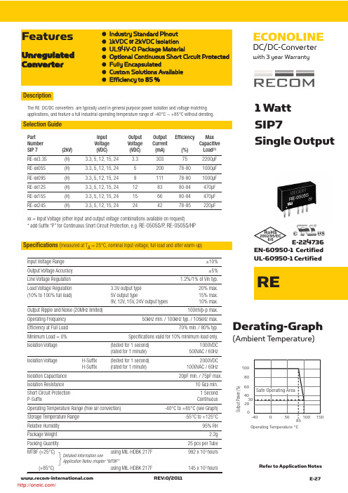
Selection GuideO u t p u t P o w e r (%)100602040Operating Temperature °C80Specifications (measured at T A = 25°C, nominal input voltage, full load and after warm-up)1 Watt SIP7Single OutputDerating-Graph(Ambient T emperature)●Industry Standard Pinout ●1kVDC or 2kVDC Isolation ●UL94V-0 Package Material●Optional Continuous Short Circuit Protected ●Fully Encapsulated●Custom Solutions Available ●Efficiency to 85%FeaturesUnregulated Converter}Detailed Information seeApplication Notes chapter "MTBF"DescriptionThe RE DC/DC converters are typically used in general purpose power isolation and voltage matching applications, and feature a full industrial operating temperature range of -40°C ~ +85°C without derating.Part Input Output Output Efficiency Max Number Voltage Voltage Current Capacitive SIP 7(2kV)(VDC)(VDC)(mA)(%)Load (1)RE-xx3.3S (H) 3.3, 5, 12, 15, 24 3.3303752200µF RE-xx05S (H) 3.3, 5, 12, 15, 24520078-801000µF RE-xx09S (H) 3.3, 5, 12, 15, 24911178-801000µF RE-xx12S (H) 3.3, 5, 12, 15, 24128380-84470µF RE-xx15S (H) 3.3, 5, 12, 15, 24156680-84470µF RE-xx24S(H)3.3, 5, 12, 15, 24244278-85220µFxx = Input Voltage (other input and output voltage combinations available on request)* add Suffix “P” for Continuous Short Circuit Protection, e.g. RE-0505S/P , RE-0505S/HPInput Voltage Range ±10%Output Voltage Accuracy ±5%Line Voltage Regulation 1.2%/1% of Vin typ.Load Voltage Regulation 3.3V output type 20% max.(10% to 100% full load)5V output type15% max.9V, 12V, 15V, 24V output types10% max.Output Ripple and Noise (20MHz limited)100mVp-p max.Operating Frequency 50kHz min. / 100kHz typ. / 105kHz max.Efficiency at Full Load 70% min. / 80% typ.Minimum Load = 0%Specifications valid for 10% minimum load only.Isolation Voltage (tested for 1 second)1000VDC (rated for 1 minute)500VAC / 60Hz Isolation Voltage H-Suffix (tested for 1 second)2000VDC H-Suffix(rated for 1 minute)1000VAC / 60Hz Isolation Capacitance 20pF min. / 75pF max.Isolation Resistance 10 G Ωmin.Short Circuit Protection 1 Second P-SuffixContinuousOperating Temperature Range (free air convection)-40°C to +85°C (see Graph)Storage Temperature Range -55°C to +125°CRelative Humidity 95% RH Package Weight2.2gPacking Quantity 25 pcs per Tube MTBF (+25°C)using MIL-HDBK 217F992 x 103 hours (+85°C)using MIL-HDBK 217F145 x 103 hoursEN-60950-1 Certified UL-60950-1 CertifiedREV:0/2011E-27 REECONOLINEDC/DC-Converterwith 3 year WarrantyRefer to Application NotesRoHS2002/95/EC6/6E-224736/E-28REV: 0/2011R E7 PIN SIP PackageXX.X ± 0.5 mm XX.XX ± 0.25 mmRE Pin Connections Pin #Single1 +Vin2 –Vin 4 –Vout 6+Vout Recommended Footprint DetailsPackage Style and Pinning (mm)3rd angle projectionTypical CharacteristicsRE SeriesECONOLINEDC/DC-ConverterE f f i c i e n c y %100040%0%100%40Efficiency / Load 60%80%20%206080Total Output current (%)Deviation / Load-10.00040%0%100%D e v i a t i o n f r o m N o m i n a l (%)60%80%20%-5.000Total Output current (%)0.0005.00010.00015.00020.00025.000E f f i c i e n c y %100040%0%100%40Efficiency / Load 60%80%20%206080Total Output current (%)E f fi c i e n c y %10040%0%100%40Efficiency / Load60%80%20%206080Total Output current (%)Deviation / Load-10.00040%0%100%D e v i a t i o n f r o m No m i n a l (%)60%80%20%-5.000Total Output current (%)0.0005.00010.00015.00020.00025.000Deviation / Load-10.00040%0%100%D e v i a t i o n f r o m N o m i n a l (%)60%80%20%-5.000Total Output current (%)0.0005.00010.00015.00020.00025.000RE-xx05SRE-xx12SRE-xx15SNotesNote 1Maximum capacitive load is defined as the capacitive load that will allow start up in under 1 second without damage to the converter.Certifications CB Test Report Report: US/15348/UL IEC 60950-1:2005 2nd Ed.UL General Safety Report: E224736UL 60950-1 1st Ed.EN General SafetyReport: IL-R7108EN60950-1:2001 + A11:2004/分销商库存信息:RECOM-POWERRE-0505S RE-0512S RE-2405SRE-0505S/P RE-1205S RE-0515SRE-2412S RE-1515S RE-0509SRE-0524S RE-053.3S RE-1209SRE-1215S RE-1224S RE-123.3SRE-0505S/H RE-0509S/H RE-0512S/H RE-0515S/H RE-0524S/H RE-053.3S/H RE-1205S/H RE-1209S/H RE-1212S/H RE-1215S/H RE-1224S/H RE-123.3S/H RE-1505S RE-1509S RE-1512SRE-1524S RE-153.3S RE-2409SRE-2424S RE-243.3S RE-3.305SRE-3.309S RE-3.312S RE-3.315SRE-3.324S RE-3.33.3S RE-0509S/P RE-0512S/P RE-0524S/P RE-053.3S/P RE-1205S/P RE-1209S/P RE-1212S/P RE-1215S/P RE-1224S/P RE-123.3S/P RE-1505S/H RE-1509S/H RE-1512S/H RE-1515S/H RE-1524S/H RE-153.3S/H RE-2405S/H RE-2409S/H RE-2412S/H RE-2415S/H RE-2424S/H RE-243.3S/H RE-3.305S/H RE-3.309S/H RE-3.312S/H RE-3.315S/H RE-3.324S/H RE-3.33.3S/H RE-1212S RE-1505S/P RE-1509S/P RE-1512S/P RE-1515S/P RE-1524S/P RE-153.3S/P RE-2405S/P RE-2409S/P RE-2412S/P RE-2415S/P RE-2424S/P RE-243.3S/P RE-3.305S/P RE-3.309S/P RE-3.312S/P RE-3.315S/P RE-3.324S/P RE-3.33.3S/P RE-0505S/HP RE-0509S/HP RE-0512S/HP RE-0515S/HP RE-0524S/HP RE-053.3S/HP RE-1205S/HP RE-1209S/HP RE-1212S/HP RE-1215S/HP RE-1224S/HP RE-123.3S/HP RE-2415S RE-0515S/P RE-1505S/HP RE-1509S/HP RE-1512S/HP RE-1515S/HP RE-1524S/HP RE-153.3S/HP RE-2405S/HP RE-2409S/HP RE-2412S/HP RE-2415S/HP RE-2424S/HP RE-243.3S/HP RE-3.305S/HP RE-3.309S/HP RE-3.312S/HP RE-3.315S/HP RE-3.324S/HP RE-3.33.3S/HP。
MSA-0504中文资料
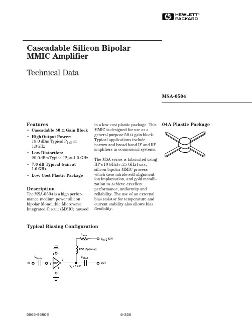
Cascadable Silicon Bipolar MMIC␣Amplifier Technical DataFeatures•Cascadable 50 Ω Gain Block •High Output Power:18.0 dBm Typical P 1 dB at 1.0␣GHz •Low Distortion:29.0 dBm Typical IP 3 at 1.0␣GHz •7.0 dB Typical Gain at 1.0␣GHz •Low Cost Plastic PackageMSA-050404A Plastic PackageDescriptionThe MSA-0504 is a high perfor-mance medium power silicon bipolar Monolithic Microwave Integrated Circuit (MMIC) housedTypical Biasing ConfigurationR V CC > 12 VINOUTin a low cost plastic package. This MMIC is designed for use as a general purpose 50 Ωgain block.Typical applications includenarrow and broad band IF and RF amplifiers in commercial systems.The MSA-series is fabricated using HP’s 10 GHz f T , 25␣GHz f MAX ,silicon bipolar MMIC process which uses nitride self-alignment,ion implantation, and gold metalli-zation to achieve excellent performance, uniformity and reliability. The use of an external bias resistor for temperature and current stability also allows bias flexibility.MSA-0504 Absolute Maximum RatingsParameterAbsolute Maximum [1]Device Current135 mA Power Dissipation [2,3] 1.5 W RF Input Power+25 dBm Junction Temperature 200°C Storage Temperature–65 to 150°CThermal Resistance [2,4]:θjc = 75°C/WNotes:1.Permanent damage may occur if any of these limits are exceeded.2.T CASE = 25°C.3.Derate at 13.3 mW/°C for T C > 88°C.4.See MEASUREMENTS section “Thermal Resistance” for more information.P 1 dB Output Power at 1 dB Gain Compression f = 0.5 GHz dBm 19.0f = 1.0 GHz dBm 16.018.0G P Power Gain (|S 21|2) f = 0.5 GHz dB7.5f = 1.0 GHz 6.07.0∆G P Gain Flatness f = 0.1 to 1.5 GHzdB ±0.75f 3 dB 3 dB Bandwidth [2]GHz2.3Input VSWR f = 0.1 to 1.5 GHz 1.6:1Output VSWRf = 0.1 to 1.5 GHz 2.0:1IP 3Third Order Intercept Point f = 1.0 GHz dBm 29.0NF 50 Ω Noise Figure f = 1.0 GHz dB 6.5t D Group Delay f = 1.0 GHz psec 180V d Device VoltageV 6.78.410.1dV/dTDevice Voltage Temperature CoefficientmV/°C–16.0Notes:1.The recommended operating current range for this device is 60 to 100 mA. Typical performance as a function of current is on the following page.2.Referenced from 0.1 GHz Gain (G P ).Electrical Specifications [1], T A = 25°CSymbolParameters and Test Conditions: I d = 80 mA, Z O = 50 ΩUnitsMin.Typ.Max.VSWRMSA-0504 Typical Scattering Parameters (T A = 25°C, I d = 80 mA)Freq.MHzMagAngdBMagAngdBMagAngMagAngk5.54–4314.7 5.43160–18.4.12037.63–390.6025.24–1129.3 2.92155–13.8.20412.24–1010.9950.18–1428.1 2.54161–13.7.2063.16–125 1.17100.14–1567.82.45166–13.7.2073.13–137 1.18200.14–1687.6 2.40163–13.7.2061.13–146 1.20400.14–1747.5 2.37150–13.7.2061.16–143 1.19600.14–1757.4 2.34137–13.6.208–1.20–144 1.18800.15–1747.2 2.29124–13.5.211–1.25–148 1.151000.17–1747.0 2.24111–13.6.209–3.29–154 1.141500.23–179 6.4 2.0980–13.3.216–4.37–168 1.062000.33171 5.5 1.8851–12.8.230–10.481780.912500.42156 4.3 1.6427–13.0.224–12.511650.903000.49146 3.2 1.446–12.8.230–11.551570.92A model for this device is available in the DEVICE MODELS section.S 11S 21S 12 S 22Typical Performance, T A = 25°C(unless otherwise noted)024681081012141618202224POWER OUT (dBm)Figure 1. Typical Gain vs. Power Out, T A = 25°C, I d = 80 mA.G A I N (d B)V S W RFREQUENCY (GHz)FREQUENCY (GHz)Figure 2. VSWR vs. Frequency,Id = 80 mA.1:12:13:14:15:16:1Figure 3. Device Current vs. Voltage.306090120I d (mA)V d (V )121418162220P 1 d B (d B m )TEMPERATURE (°C)Figure 4. Output Power at 1 dB Gain Compression, vs. Case Temperature, I d = 80 mA.18–25+25+85P 1 d B (d B m )I d (mA)Figure 6. Output Power at 1 dB Gain Compression, Third Order Intercept vs. Current, f = 1.0 GHz.Figure 5. Gain vs. Frequency,I d = 80 to 100 mA.60708090100I P 3 (d B m )0.5 GHz1.0 GHz2.0 GHz.01.050.10.5 1.05.014121086420G p (d B )04A Plastic Package Dimensions0.76 (0.030)2.54 ± 0.250.51 DIMENSIONS ARE IN MILLIMETERS (INCHES).RF OUTPUT& BIASmm .XX = ± 0.13 in .XXX = ± 0.005。
REF5045中文资料

REF5020, REF5025 REF5030, REF5040 REF5045, REF5050
SBOS410 – JUNE 2007
ELECTRICAL CHARACTERISTICS: PER DEVICE
Boldface limits apply over the specified temperature range, TA = –40°C to +125°C. At TA = +25°C, ILOAD = 0, CL = 1μF, and VIN = (VOUT + 0.2V) to 18V, unless otherwise noted.
2
Copyright © 2007, Texas Instruments Incorporated
Submit Documentation Feedback
Product Folder Link(s): REF5020 REF5025 REF5030 REF5040 REF5045 REF5050
元器件交易网
元器件交易网
REF5020, REF5025 REF5030, REF5040 REF5045, REF5050
SBOS410 – JUNE 2007
Low-Noise, Very Low Drift, Precision VOLTAGE REFERENCE
SO-8 MSOP-8 (2)
SO-8 MSOP-8 (2)
SO-8 MSOP-8 (2)
SO-8 MSOP-8 (2)
SO-8 MSOP-8 (2)
SO-8 MSOP-8 (2)
SO-8 MSOP-8 (2)
SO-8 MSOP-8 (2)
2N5484中文资料

**L2 **L3
6 turns, (approx. — depends upon circuit layout) AWG #24 enameled copper wire, close wound on 7/32″ ceramic coil form. Tuning provided by an aluminum slug. 1 turn, AWG #16 enameled copper wire, 3/8″ I.D. (AIR CORE). 1/2 turn, AWG #16 enameled copper wire, 1/4″ I.D. (AIR CORE).
POWER GAIN
24 f = 100 MHz
20 PG , POWER GAIN (dB)
16
12
400 MHz Tchannel = 25°C VDS = 15 Vdc VGS = 0 V 0 2.0 4.0 6.0 8.0 10 ID, DRAIN CURRENT (mA) 12 14
8.0 4.0
Figure 2. 100 MHz and 400 MHz Neutralized Test Circuit
NOISE FIGURE
(Tchannel = 25°C)
10 ID = 5.0 mA 8.0 NF, NOISE FIGURE (dB) NF, NOISE FIGURE (dB) 5.5 6.5 VDS = 15 V VGS = 0 V
1 2 3
CASE 29–04, STYLE 5 TO–92 (TO–226AA)
ELECTRICAL CHARACTERISTICS (TA = 25°C unless otherwise noted)
RCLAMP0522P中文资料
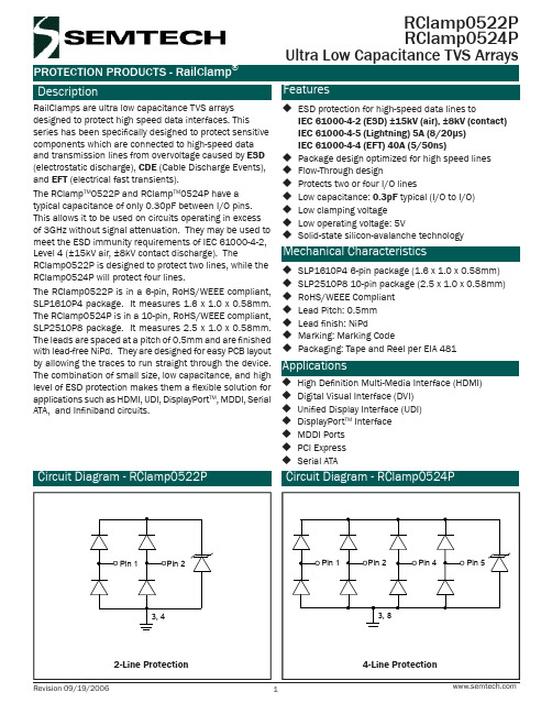
Applications
High Definition Multi-Media Interface (HDMI) Digital Visual Interface (DVI) Unified Display Interface (UDI) DisplayPortTM Interface MDDI Ports PCI Express Serial ATA
RClamp0522P RClamp0524P
PRELIMINARY
Power Derating Curve
110 100 90 80 70 60 50 40 30 20 10 0
PROTECTION PRODUCTS Typical Characteristics
Non-Repetitive Peak Pulse Power vs. Pulse Time
Pin 1
Pin 2
Pin 1
Pin 2
Pin 4
Pin 5
3, 4
3, 8
Circuit Diagram
Circuit Diagram
Ordering Information
Part Number RClamp0522P.TCT RClamp0524P.TCT Number of Lines Qty per Reel Reel Size 7 Inch 7 Inch
PRELIMINARY
RClamp0522P RClamp0524P
RClamp0524P
10 9 8 7 6
1
Pin 1-2 5-6 3-4
2
3
Identification Input Lines Output Lines (No Internal Connection) Ground Pin
RCLAMP0524J.TCT中文资料

Cj
Conditions
Any I/O pin to ground
It = 1mA Any I/O pin to ground
VRWM = 5V, T=25°C Any I/O pin to ground
IPP = 1A, tp = 8/20μs Any I/O pin to ground
V = 0V, f = 1MHz R
Dimensions
Circuit Diagram
2.70 0.40
12
1.00
0.60 0.20
0.50
0.58
Pin 1
Pin 2
Pin 3
Pin 4
GND
Nominal Dimensions in mm
Revision 02/05/2008
1
4-Line Protection
3 2: -0.062 dB
1
2
1.8 GHz
3: -0.1087 dB 2.5 GHz
100 MHz
13 GHz GHz
STOP 3000.000000 MHz
RClamp0524J
PRELIMINARY
Insertion Loss S21 - I/O to GND
CH1 S21 LOG 6 dB / REF 0 dB
Mechanical Characteristics
SLP2710P8 8-pin package (2.7 x 1.0 x 0.58mm) RoHS/WEEE Compliant Lead Pitch: 0.5mm Lead finish: NiPdAu Marking: Marking Code Packaging: Tape and Reel per EIA 481
HNC-050P资料

Electrical dataPrimary nominal Primary current TypeDC current measuring range IPN(A)I P(A)500 .. ± 75HNC - 050P 1000 .. ± 140HNC - 100PHNC - 050P HNC - 100PR M Measuing resistance 60 .. 9060 .. 80ΩI SN Second nominal current 5050mA K N Turns ratio 1 : 1000 1 : 2000V C Supply voltage (± 5 %) ± 15V I C Current consumpution 15 + I SN mA V dR.m.s. voltage for AC isolation test, 50/60Hz, 1 min 2.5kVAccuracy-Dynamic performance dataXAccuracy @ T A = 25°C ± 1% of I PNεLLinearity (0 .. ± I PN )< ± 0.5%I O Electrical offset current @I P = 0, @T A = 25°C ± 0.2mA I HC Hysteresis offset current @ I P = 0,after an excursion of I PN ± 0.15mA I OT Thermal drift of I O 0°C .. +70°C ± 0.005ms/°C t rResponse time @ 90% of I P <1 µs TC εGThermal drift of the gain (% of reading) < ± 0.004%/°CGeneral dataT A Ambient operating temperature - 10 .. + 80°C T S Ambient storage temperature- 15 .. + 85°CHNC - 200PHNC - 300PR S Secondary coil Resistance@T A = 25°C 7595ΩmMass30gCurrent Transducer HNC- 050 .. 100PFor the electronic measurement of currents: DC, AC, pulsed, mixed,with a galvanic isolation between the primary circuit (high power) and the secondary circuit (electronic circuit).I PN = 50 .. 100 AFeatures• Hall effect measuring principle• Galvanic isolation between primaryand secondary circuit • Isolation voltage 2500 V • Low power consumptionAdvantages• Easy mounting• Small size and space saving • Only one design for wide currentratings range•High immunity to external interferenceApplications• DC motor drives• Switched Mode Power Supplies(SMPS)• AC variable speed drives• Uninterruptible Power Supplies (UPS)• Battery supplied applications • Inverterswww.nanalem.co.jp010301/1HNC- 050 .. 100PNANALEM reserves the right to carry out modifications on its transducers, in order to improve them, without previous notice.UNIT: mm。
74435561100;中文规格书,Datasheet资料

74435561100
DATUM / DATE : 2009-11-02 Gurtspezifikation / Tape specification:
G H
SPEICHERDROSSEL WE-HCI POWER-CHOKE WE-HCI
I Rollenspezifikation / tape and reel specification:
74435561100
DATUM / DATE : 2009-11-02
SPEICHERDROSSEL WE-HCI POWER-CHOKE WE-HCI
H Induktivitätskurve / Inductance curve:
Induktivität vs Strom (typ.) Inductance vs Current (typ.)
08-09-29
Geprüft / checked
Kontrolliert / approved
Datum / date
D-74638 Waldenburg · Max-Eyth-Strasse 1 - 3 · Germany · Telefon (+49) (0) 7942 - 945 - 0 · Telefax (+49) (0) 7942 - 945 - 400 http://www.we-online.de
12,00
10,00
8,00
L (µH)
6,00
4,00
2,00
0,00 0 5 10 15 Current (A) 20 25 30 35
Freigabe erteilt / general release:
..................................................................................
RCLamp0508M.TBT资料

1.8 1.6 1.4 1.2 1 0.8 0.6 0.4 0.2 0 0 1 2 3 4 f = 1 MHz 5
2.00
4.00
6.00
8.00
10.00
12.00
Forward Current - IF (A)
Reverse Voltage - VR (V)
Power Derating Curve
Peak Pulse Power - PPP (kW)
1
0.1
0.01 0.1 1 10 Pulse Duration - tp (µs) 100 1000
0
25
50
75
100
125
150
Ambient Temperature - TA (oC)
Pulse Waveform
30.00 Clamping Voltage -Vc (V) 25.00 20.00 15.00 10.00 5.00 0.00 0.00 Waveform Parameters: tr = 8µs td = 20µs 2.00 4.00 6.00 8.00 10.00 12.00
Percent of I
CH1 S21 LOG 20 dB/ REF 0 dB
START
.030 000 MHz
STOP 3 RT
.030 000 MHz
STOP 3 000. 000 000 MHz
2008 Semtech Corp.
4
RClamp0508M
e-t
Peak Pulse Current - Ipp (A)
Forward Voltage vs. Forward Current
RCLAMP0502N中文资料
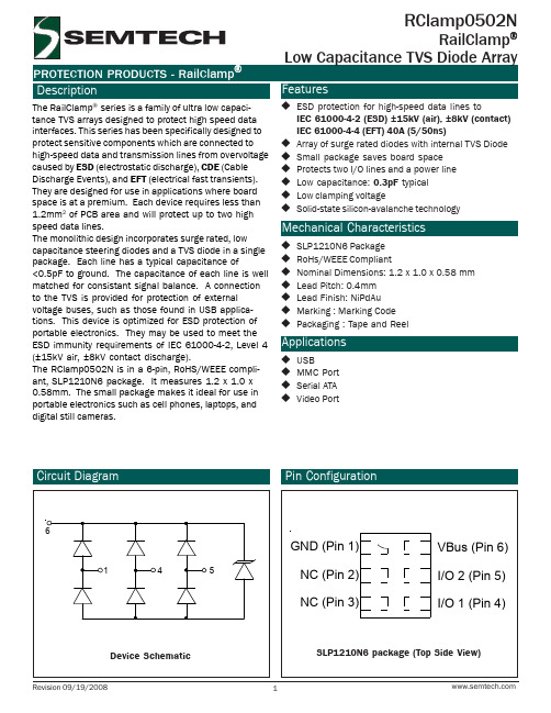
1.6
1.4
1.2
1
0.8
0.6
0.4
0.2 f = 1 MHz
0
0
1
2
3
4
5
6
7
Reverse Voltage - VR (V)
CJ(VR) / CJ(VR=0)
CJ(VR) / CJ(VR=0)
Forward Voltage - VF V)
% of Rated Power or IPP
RClamp0502N
40
35
30
25
20
15
Waveform
10
Parameters:
tr = 8μs
5
td = 20μs
0
0
0.5
1
1.5
2
2.5
3
3.5
4
Peak Pulse Current - IPP (A)
Normalize Capacitance vs. Reverse Voltage I/O to Gnd - Pin 4, 5 to Pin 1
Forward Voltage
VF
If = 15mA
Any I/O to pin 6
Clamping Voltage
VC
IPP = 1A, tp = 8/20μs
Any I/O pin to Ground
Clamping Voltage
VC
IPP = 3A, tp = 8/20μs
Any I/O pin to Ground
RClamp0502N
RailClamp® Low Capacitance TVS Diode Array
RCLAMP0524P描述及应用
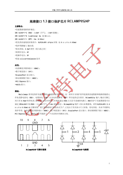
高清接口1.3接口保护芯片RCLAMP0524P主要特点:•高速数据线路保护满足:IEC61000-4-2(ESD)±15kV(空气),±8kV(接触);IEC61000-4-5(Lightning)5A(8/20μs);IEC61000-4-4(EFT)40A(5/50ns)•优化的高速线流封装设计:SLP2510P810-pin封装(2.5x 1.0x0.58mm)•保护四路输入/输出线•低电容值:0.3pf典型(线与线之间)•低钳位电压:6V•低操作电压:5V•固态silicon-avalanche技术应用:•高清晰度多媒体接口(HDMI);•数字视觉接口(DVI);•DisplayPort显示接口;•移动视频数字接口(MDDI);•PCI Express接口;•eSATA接口;描述:Railclamps系列是保护高速数据接口的超低电容TVS管。
这一系列专为保护某些连接到高速数据和线路的敏感元件免受静电放电(ESD)、电缆放电(CDE)以及电快速瞬变(EFT)所引起的过压损害。
Rclam0524p输入/输出引脚之间只有0.30pf典型电容,这使得它可以应用在工作频率超过3GHZ且无信号衰减的电路上,ESD防护于高速数据线可以满足IEC61000-4-2(ESD)(±15kV空气,±8kv接触放电)。
Rclamp0524p保护4条I/O数据线,采用SLP2510P8(2.5 x1.0x0.58mm)10引脚封装,便于电路板贴片机流水式生产,正是由于其具备小尺寸封装,低电容值,高水平的静电保护作用,为高清晰度多媒体接口(HDMI)、数字视觉接口(DVI)、DisplayPort显示接口、移动视频数字接口(MDDI)、PCI Express接口、eSATA接口等提供了一个灵活的应用解决方案。
引脚示意图Rclamp0524P电路图Rclamp0524P在HDMI接口的应用。
RCLAMP0502B中文资料
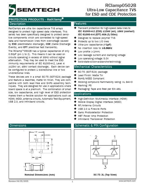
Clamping Voltage Clamping Voltage Clamping Voltage Junction Capacitance Junction Capacitance
Symbol V
RWM
VBR
IR
VC VC VC Cj Cj
Conditions
Pin 1 or Pin 2 to Pin 3 and Between Pins 1 and 2
It =1mA Pin 1 or Pin 2 to Pin 3 and Between Pins 1 and 2
VRWM = 5V, T=25°C Pin 1 or Pin 2 to Pin 3 and Between Pins 1 and 2
ESD Response (4kV Contact per IEC 61000-4-2)
RClamp0502B
Insertion Loss S21 (Pin 1 or Pin 2 to Pin 3)
CH1 S21 LOG 6 dB / REF 0 dB
0 dB -6 dB
1: .00460 dB 900 MHz
Applications
High-Definition Multimedia Interface (HDMI) Mobile Display Digital Interface (MDDI) RF/Antenna Circuits USB 2.0 & Firewire Ports GaAs Photodetector Protection HBT Power Amp Protection Infiniband Transceiver Protection
5804中文资料

5804中⽂资料Combining low-power CMOS logic with high-current and high-voltage bipolar outputs, the UCN5804B and UCN5804LB BiMOS II translator/drivers provide complete control and drive for a four-phase unipolar stepper-motor with continuous output current ratings to 1.25 A per phase (1.5 A startup) and 35 V.The CMOS logic section provides the sequencing logic, DIRECTION and OUTPUT ENABLE control, and a power-on reset function. Three stepper-motor drive formats, wave-drive (one-phase), two-phase, and half-step are externally selectable. The inputs are compatible with standard CMOS, PMOS, and NMOS circuits. TTL or LSTTL may require the use of appropriate pull-up resistors to ensure a proper input-logic high.The wave-drive format consists of energizing one motor phase at a time in an A-B-C-D (or D-C-B-A) sequence. This excitation mode consumes the least power and assures positional accuracy regardless of any winding inbalance in the motor. Two-phase drive energizes two adjacent phases in each detent position (AB-BC-CD-DA). This sequence mode offers animproved torque-speed product, greater detent torque, and is less susceptible to motor resonance. Half-step excitation alternates between the one-phase and two-phase modes (A-AB-B-BC-C-CD-D-DA), providing an eight-step sequence.The bipolar outputs are capable of sinking up to 1.5 A and withstanding 50 V in the off state (sustaining voltages up to 35 V). Ground-clamp and flyback diodes provide protection against inductive transients. Thermal protection circuitry disables the outputs when the chip temperature is exces-sive.Both devices are rated for operation over the temperature range of -20°C to +85°C. The UCN5804B is supplied in a 16-pin dual in-line plastic batwing package with a copper lead frame and heat-sinkable tabs for improved power dissipation capabilities; the UCN5804LB is supplied in a 16-lead plastic SOIC batwing package with a copper lead frame and heat-sinkable tabs.FEATURESI 1.5 A Maximum Output Current I 35 V Output Sustaining VoltageI Wave-Drive, Two-Phase, and Half-Step Drive Formats I Internal Clamp DiodesI Output Enable and Direction Control I Power-On ResetI Internal Thermal Shutdown CircuitryBiMOS II UNIPOLARSTEPPER-MOTOR TRANSLATOR/DRIVERAlways order by complete part number, e.g., UCN5804B .Data Sheet 26184.12C*5804115 Northeast Cutoff, Box 15036Worcester, Massachusetts 01615-0036 (508) 853-********BiMOS II UNIPOLAR STEPPER-MOTORTRANSLATOR/DRIVERTRUTH TABLEDrive Format Pin 9Pin 10Two-Phase L L One-Phase H L Half-Step L H Step-InhibitHHTYPICAL INPUT CIRCUITDwg. EP-021-4TYPICAL OUTPUT DRIVERDwg. EP-010-5INCopyright ? 1987, 2000 Allegro MicroSystems, Inc.5075100125150510A L L O W A B L E P A C K A G E P O W E R D I S S I P A T I O N I N W A T T STEMPERATURE IN °C43225Dwg. GP-049-2A5804BiMOS II UNIPOLAR STEPPER-MOTOR TRANSLATOR/DRIVER/doc/a3712eddb9f3f90f76c61b7c.htmlELECTRICAL CHARACTERISTICS at T A = 25°C, T J ≤ 150°C, V DD = 4.5 V to 5.5 V (unless otherwise noted). Limits CharacteristicSymbol Test Conditions Min.Typ.Max.Units Output Leakage Current I CEX V OUT = 50 V—1050µA Output Sustaining Voltage V CE(sus)I OUT = 1.25 A, L = 3 mH 35——V Output Saturation VoltageV CE(SAT)I OUT = 700 mA — 1.0 1.2V I OUT = 1 A — 1.1 1.4V I OUT= 1.25 A— 1.2 1.5V Clamp Diode Leakage Current I R V R = 50 V —1050µA Clamp Diode Forward Voltage V F I F = 1.25 A — 1.53.0V Input CurrentI IN(1)V IN = V DD —0.5 5.0µA I IN(0)V IN = 0.8 V —-0.5-5.0µA Input VoltageV IN(1)V DD = 5 V3.5— 5.3V V IN(0)-0.3—0.8V Supply Current I DD 2 Outputs ON—2030mA Turn-Off Delay t ON 50% Step Inputs to 50% Output ——10µs Turn-On Delayt OFF 50% Step Inputs to 50% Output ——10µs Thermal Shutdown TemperatureT J—165—°CTIMING CONDITIONSA. Minimum Data Set Up Time . . . . . . . . . . . . . . . . . . . . . . . . 100 nsB. Minimum Data Hold Time . . . . . . . . . . . . . . . . . . . . . . . . . . 100 nsC. Minimum Step Input Pulse Width . . . . . . . . . . . . . . . . . . . . . 3.0 µsDwg. W-110AONE PHASE HALF STEPOOUTPUT ENABLEOUTPUT C OUTPUT DCLOCK115 Northeast Cutoff, Box 15036Worcester, Massachusetts 01615-0036 (508) 853-50005804BiMOS II UNIPOLAR STEPPER-MOTORTRANSLATOR/DRIVERWAVE-DRIVE SEQUENCEHalf Step = L, One Phase = H Step A B C D POR ON OFF OFF OFF 1ON OFF OFF OFF 2OFF ON OFF OFF 3OFF OFF ON OFF 4OFFOFFOFFONTWO-PHASE DRIVE SEQUENCEHalf Step = L, One Phase = LStep A B C D POR ON OFF OFF ON 1ON OFF OFF ON 2ON ON OFF OFF 3OFF ON ON OFF 4OFFOFFONONHALF-STEP DRIVE SEQUENCEHalf Step = H, One Phase = LStep A B C D POR ON OFF OFF OFF 1ON OFF OFF OFF 2ON ON OFF OFF 3OFF ON OFF OFF 4OFF ON ON OFF 5OFF OFF ON OFF 6OFF OFF ON ON 7OFF OFF OFF ON 8ONOFFOFFONAPPLICATIONS INFORMATIONInternal power-on reset (POR) circuitry resets OUTPUT A (and OUTPUT D in the two-phase drive format) to the on state with initial applica-tion of the logic supply voltage. After reset, the circuit then steps according to the tables.The outputs will advance one sequenceposition on the high-to-low transition of the STEP INPUT pulse. Logic levels on the HALF-STEP and ONE-PHASE inputs will determine the drive format (one-phase, two-phase, or half-step). The DIRECTION pin determines the rotation se-quence of the outputs. Note that the STEP INPUT must be in the low state when changing the state of ONE-PHASE, HALF-STEP, or DIRECTION to prevent erroneous stepping.All outputs are disabled (off) when OUTPUT ENABLE is at a logic high. If the function is not required, OUTPUT ENABLE should be tied low.In that condition, all outputs depend only on the state of the step logic.During normal commutation of a unipolar stepper motor, mutual coupling between the motor windings can force the outputs of the UCN5804B below ground. This condition will cause forward biasing of the collector-to-substrate junction and source current from the output. For many L/R applications, this substrate current is high enough to adversely affect the logic circuitry and cause misstepping. External series diodes (Schottky are recommended for increasedefficiency at low-voltage operation) will prevent substrate current from being sourced through the outputs. Alternatively, external ground clamp diodes will provide a preferred current path from ground when the outputs are pulled below ground.Internal thermal protection circuitry disables all outputs when the junction temperature reaches approximately 165°C. The outputs are enabled again when the junction cools down to approxi-mately 145°C.5804BiMOS II UNIPOLAR STEPPER-MOTOR TRANSLATOR/DRIVER/doc/a3712eddb9f3f90f76c61b7c.htmlTYPICAL APPLICATION L/R Stepper-Motor DriveThe products described here are manufactured under one or more U.S. patents or U.S. patents pending.Allegro MicroSystems, Inc. reserves the right to make, from time to time, such departures from the detail specifications as may berequired to permit improvements in the performance, reliability, or manufacturability of its products. Before placing an order, the user is cautioned to verify that the information being relied upon is current.Allegro products are not authorized for use as critical components in life-support devices or systems without express written approval.The information included herein is believed to be accurate and reliable. However, Allegro MicroSystems, Inc. assumes no responsi-bility for its use; nor for any infringement of patents or other rights of third parties which may result from its use.115 Northeast Cutoff, Box 15036Worcester, Massachusetts 01615-0036 (508) 853-50005804BiMOS II UNIPOLAR STEPPER-MOTORTRANSLATOR/DRIVERUCN5804BDimensions in Inches (controlling dimensions)Dimensions in Millimeters(for reference only)NOTES:1.Exact body and lead configuration at vendor’s option within limits shown.2.Lead spacing tolerance is non-cumulative.3.Lead thickness is measured at seating plane or below.4.Webbed lead frame. Leads 4, 5, 12, and 13 are internally one piece.5.Supplied in standard sticks/tubes of 25 devices.Dwg. MA-001-17A in18Dwg. MA-001-17A mm185804 BiMOS II UNIPOLAR STEPPER-MOTOR TRANSLATOR/DRIVER/doc/a3712eddb9f3f90f76c61b7c.htmlUCN5804LB(add “TR” to part number for tape and reel) Dimensions in Inches(for reference only)Dimensions in Millimeters(controlling dimensions)NOTES:1.Exact body and lead configuration at vendor’s option within limits shown.2.Lead spacing tolerance is non-cumulative.3.Lead thickness is measured at seating plane or below.4.Webbed lead frame. Leads 4, 5, 12, and 13 are internally one piece.5.Supplied in standard sticks/tubes of 47 devices or add “TR” to part number for tape and reel.115 Northeast Cutoff, Box 15036Worcester, Massachusetts 01615-0036 (508) 853-50005804BiMOS II UNIPOLAR STEPPER-MOTORTRANSLATOR/DRIVERMOTOR DRIVERSFunctionOutput Ratings*Part Number ?INTEGRATED CIRCUITS FOR BRUSHLESS DC MOTORS3-Phase Power MOSFET Controller —28 V 39333-Phase Power MOSFET Controller —50 V 39323-Phase Power MOSFET Controller —50 V 76002-Phase Hall-Effect Sensor/Driver 400 mA 26 V 3626Bidirectional 3-Phase Back-EMFController/Driver ±600 mA 14 V 89062-Phase Hall-Effect Sensor/Driver 900 mA 14 V 36253-Phase Back-EMFController/Driver ±900 mA 14 V 8902–A 3-Phase Controller/Drivers ±2.0 A 45 V 2936 & 2936-120INTEGRATED BRIDGE DRIVERS FOR DC AND BIPOLAR STEPPER MOTORSDual Full Bridge with Protection & Diagnostics ±500 mA 30 V 3976PWM Current-Controlled Dual Full Bridge ±650 mA 30 V 3966PWM Current-Controlled Dual Full Bridge ±650 mA 30 V 3968PWM Current-Controlled Dual Full Bridge ±750 mA 45 V 2916PWM Current-Controlled Dual Full Bridge ±750 mA 45 V 2919PWM Current-Controlled Dual Full Bridge ±750 mA 45 V 6219PWM Current-Controlled Dual Full Bridge ±800 mA 33 V 3964PWM Current-Controlled Full Bridge ±1.3 A 50 V3953PWM Current-Controlled Dual Full Bridge ±1.5 A 45 V 2917PWM Current-Controlled Microstepping Full Bridge ±1.5 A 50 V 3955PWM Current-Controlled Microstepping Full Bridge ±1.5 A 50 V 3957PWM Current-Controlled Dual DMOS Full Bridge ±1.5 A 50 V 3972Dual Full-Bridge Driver ±2.0 A 50 V 2998PWM Current-Controlled Full Bridge ±2.0 A 50 V3952DMOS Full Bridge PWM Driver ±2.0 A 50 V 3958Dual DMOS Full Bridge ±2.5 A 50 V 3971UNIPOLAR STEPPER MOTOR & OTHER DRIVERSVoice-Coil Motor Driver ±500 mA 6 V 8932–A Voice-Coil Motor Driver ±800 mA 16 V 8958Unipolar Stepper-Motor Quad Drivers 1 A 46 V 7024 & 7029Unipolar Microstepper-Motor Quad Driver 1.2 A 46 V 7042Unipolar Stepper-Motor Translator/Driver 1.25 A 50 V 5804Unipolar Stepper-Motor Quad Driver 1.8 A 50 V 2540Unipolar Stepper-Motor Quad Driver 1.8 A 50 V 2544Unipolar Stepper-Motor Quad Driver 3 A 46 V 7026Unipolar Microstepper-Motor Quad Driver 3 A 46 V 7044*Current is maximum specified test condition, voltage is maximum rating. See specification for sustaining voltage limits or over-current protection voltage limits. Negative current is defined as coming out of (sourcing) the output.?Complete part number includes additional characters to indicate operating temperature range and package style.Also, see 3175, 3177, 3235, and 3275 Hall-effect sensors for use with brushless dc motors.。
RCLAMP0504F中文资料
e-t
td = IPP/2
5
10
15
20
25
30
Time (µs)
Forward Voltage vs. peak Pulse Current
8
7
6
5
4
3
Waveform
2
Parameters:
tr = 8µs
1
td = 20µs
0
0
1
2
3
4
5
6
Peak Pulse Current - IPP (A)
25
V
3
pF
1.5
pF
© 2008 Semtech Corp.
2
元器件交易网
PROTECTION PRODUCTS Typical Characteristics
Non-Repetitive Peak Pulse Power vs. Pulse Time
IPP = 6A, tp = 8/20μs Any pin to pin 2
VR = 0V, f = 1MHz Any I/O pin to pin 2
V = 0V, f = 1MHz R
Between I/O pins
Minimum 6
Typical
Maximum 5
Units V V
3
μA
15
V
RClamp0504F
Insertion Loss S21 (I/O to I/O)
CH1 S21 LOG 6 dB / REF 0 dB
START. 030 MHz
STOP 3000.000000 MHz
常见荧光定量PCR仪汇总[专家学习]
![常见荧光定量PCR仪汇总[专家学习]](https://img.taocdn.com/s3/m/2fede4710975f46526d3e113.png)
具有独特的Veriflex TM 加块,控温效果大大提高
理论支持本公司PCR体系:30ul 一类特制
28
优缺点:
ABI ViiA7
ABI第7代产品,优点比7900有所提升,理论支持本公司PCR体系:40ul 1.检测孔数:96孔板,384孔板,Taqman 低密度表达谱芯片 2.激发光源:齿钨灯 3.加热模块:半导体加热模块,升温3℃/S,温控准确性好。 4.运行时间:35min完成40个循环。 5.检测通道:6通道,除去ROX后5通道
一类特制
42
Bio-rad DNA Engine Opticon 2
优缺点:由DNA Engine和光学模块组成
1.检测孔数:96孔板 或 8联管
2.激发光源:LED单激发光源,双通道检测
3.加热模块:DNA Engine 升温3℃/S
4.运行时间:2h完成40个循环。
5.检测通道:2通道,无需ROX校正
光路:LED激发+PMT检测
其中3310为单通道检测(FAM),支持两种荧光染料 (FAM/SYBR)
而3320为双通道检测(FAM,HEX)一,类支特制持三种荧光染料
47
杭州 博日FQD-48a
性能描述
FQD-48a具有单通道和4通道两种规格,通 过硬件转换可升级至4通道,支持0.2mlPCR 管,支持本公司体系:40ul
6.可以脱离电脑控制,独立运行
7.具有温度梯度功能,最高可达24℃
8.具有mini Opticon 产品 48孔
一类特制
43
Chromo 4
优缺点:由DNA Engine和光学模块组成
1.检测孔数:96孔板 或 8联管 2.激发光源:4个LED 3.加热模块:DNA Engine的Alpha 升温3℃/S 4.运行时间:2h完成40个循环。 5.检测通道:4通道,无需ROX校正 6.可以脱离电脑控制,独立运行 7.具有温度梯度功能,最高可达24℃
- 1、下载文档前请自行甄别文档内容的完整性,平台不提供额外的编辑、内容补充、找答案等附加服务。
- 2、"仅部分预览"的文档,不可在线预览部分如存在完整性等问题,可反馈申请退款(可完整预览的文档不适用该条件!)。
- 3、如文档侵犯您的权益,请联系客服反馈,我们会尽快为您处理(人工客服工作时间:9:00-18:30)。
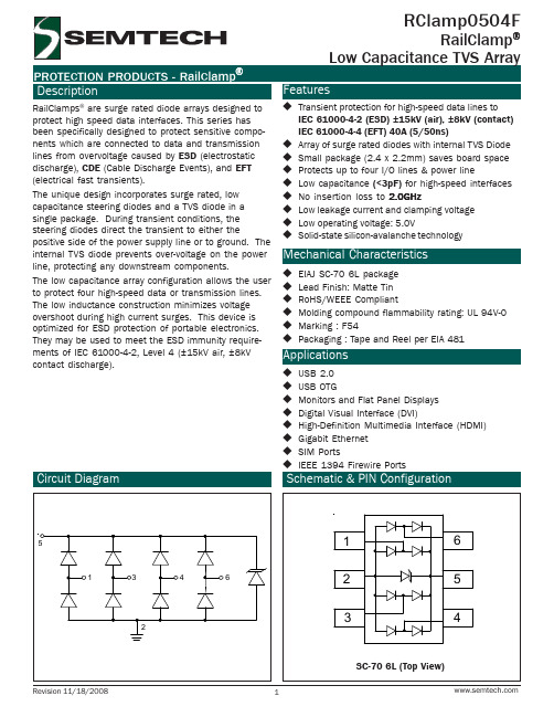
RailClamps are surge rated diode arrays designed to protect high speed data interfaces. This series has been specifically designed to protect sensitive components which are connected to data and transmission lines from overvoltage caused by ESD (electrostatic discharge), CDE (Cable Discharge Events), and EFT (electrical fast transients). The unique design incorporates surge rated, low capacitance steering diodes and a TVS diode in a single package. During transient conditions, the steering diodes direct the transient to either the positive side of the power supply line or to ground. The internal TVS diode prevents over-voltage on the power line, protecting any downstream components. The low capacitance array configuration allows the user to protect four high-speed data or transmission lines. The low inductance construction minimizes voltage overshoot during high current surges. This device is optimized for ESD protection of portable electronics. They may be used to meet the ESD immunity requirements of IEC 61000-4-2, Level 4 (±15kV air, ±8kV contact discharge).
RClamp0504S
Mechanical Characteristics
JEDEC SOT-23 6L package Nominal Dimensions: 2.9x2.8mm RoHS/WEEE Compliant Molding compound flammability rating: UL 94V-0 Marking: Marking Code Packaging: Tape and Reel USB 2.0 USB OTG Monitors and Flat Panel Displays Digital Visual Interface (DVI) Gigabit Ethernet IEEE 1394 Firewire Ports
Non-Repetitive Peak Pulse Power vs. Pulse Time
10
110 100 90 80 70 60 50 40 30 20 10 0
Power Derating Curve
Peak Pulse Power - P PP (kW)
1
0.1
0.01 0.1 1 10 Pulse Duration - tp (µs) 100 1000
Clamping Voltage vs. Peak Pulse Current
Waveform Parameters: tr = 8µs td = 20µs
30 25 Clamping Voltage - VC (V) 20 15
Line to Ground
Line to Line
Percent of I
1 2 3 4
Insertion Loss S21 (I/O to I/O)
CH1 S21 LOG 6 dB / REF 0 dB 1: -0.1063 dB 900 MHz 2: -0.2660 dB 1.8 GHz 3: -0.5657 dB 2.5 GHz 0 dB
1 2 3
-6 dB -12 dB -18 dB -24 dB -30 dB -36 dB 1 MHz START . 030 MHz 10 MHz 100 MHz
4: -3.3538 dB 2.5 GHz
-6 dB -12 dB -18 dB -24 dB -30 dB
3 1 GHz GHz STOP 3000. 000000 MHz
-36 dB
1 MHz START . 030 MHz
10 MHz
100 MHz
3 1 GHz GHz STOP 3000. 000000 MHz
f = 1 MHz
0 0 1 2 3 Reverse Voltage - VR (V) 4 5
2008 Semtech Corp.
3
RClamp0504S
PROTECTION PRODUCTS
Insertion Loss S21 (I/O to Pin 2)
CH1 S21 LOG 6 dB / REF 0 dB 1: -0.1801 dB 900 MHz 2: -0.6816 dB 1.8 GHz 3: -3.0407 dB 2.448 GHz 0 dB
Normalized Junction Capacitance vs. Reverse Voltage
1.4 1.2 CJ(VR) / CJ(VR=0) 1 0.8 0.6 0.4 0.2
5 4 3 2 1 0 0 1 2 3 4 5 6 Peak Pulse Current - IPP (A) Waveform Parameters: tr = 8µs td = 20µs
RailClamp Low Capacitance TVS Array
Features
Transient protection for high-speed data lines to
IEC 61000-4-2 (ESD) ±15kV (air), ±8kV (contact) IEC 61000-4-4 (EFT) 40A (5/50ns) Array of surge rated diodes with internal TVS Diode Small package saves board space Protects up to four I/O lines & power line Low capacitance (<3pF) for high-speed interfaces No insertion loss to 2.0GHz Low leakage current and clamping voltage Low operating voltage: 5.0V Solid-state silicon-avalanche technology
Symbol VRWM V BR IR VC VC Cj
Conditions Pi n 5 to 2 It = 1mA Pi n 5 to 2 VRWM = 5V, T=25°C Pi n 5 to 2 IPP = 1A, tp = 8/20µs A n y p i n to p i n 2 IPP = 6A, tp = 8/20µs A n y p i n to p i n 2 VR = 0V, f = 1MHz Any I/O p in to p in 2 VR = 0V, f = 1MHz Between I/O p ins
R ating Peak Pulse Power (tp = 8/20µs) Peak Pulse Current (tp = 8/20µs) ESD p er IEC 61000-4-2 (Air) ESD p er IEC 61000-4-2 (Contact) Op erating Temp erature Storage Temp erature Symbol Pp k IP P VESD TJ TSTG Value 150 6 15 8 -55 to +125 -55 to +150 Units Watts A kV °C °C
e-t
td = IPP/2
10 5
Waveform Parameters: tr = 8µs td = 20µs
0
1
2 3 4 5 Peak Pulse Current - IPP (A)
6
7
Forward Voltage vs. Peak Pulse Current
8 7 Forward Voltage - V F (V) 6
% of Rated Power or IPP
0
25
50
75
100
125
150
Ambient Temperature - TA (oC)
Pulse Waveform
110 100 90 80 70 60 50 40 30 20 10 0 0 5 10 15 Time (µs) 20 25 30
0
PP
Analog Crosstalk
CH1 S21 LOG 20 dB / REF 0 dB
ESD Clamping (+8kV Contact per IEC 61000-4-2)
START . 030 MHz
