TIP137中文资料
100371中文资料
100371中⽂资料100371Low Power Triple 4-Input Multiplexer with EnableGeneral DescriptionThe 100371contains three 4-input multiplexers which share a common decoder (inputs S 0and S 1).Output buffer gates provide true and complement outputs.A HIGH on the Enable input (E)forces all true outputs LOW (see Truth Table).All in-puts have 50k ?pull-down resistors.Featuresn 35%power reduction of the 100171n 2000V ESD protectionn Pin/function compatible with 100171n Voltage compensated operating range =?4.2V to ?5.7V nAvailable to MIL-STD-883Logic SymbolPin Names DescriptionI 0x –I 3x Data Inputs S 0,S 1Select InputsE Enable Input (Active LOW)Z a –Z c Data OutputsZ a –Z cComplementary Data OutputsDS100975-1September 1998100371Low Power Triple 4-Input Multiplexer with Enable1998National Semiconductor Corporation /doc/8316005118.htmlConnection DiagramsLogic Diagram24-Pin DIPDS100975-224-Pin Quad CerpakDS100975-3DS100975-5/doc/8316005118.html2Truth TableInputs OutputsE S0S1Z nL L L I0xL H L I1xL L H I2xL H H I3xH X X LH=HIGH Voltage LevelL=LOW Voltage LevelX=Don’t Care3/doc/8316005118.htmlAbsolute Maximum Ratings (Note 1)If Military/Aerospace specified devices are required,please contact the National Semiconductor Sales Office/Distributors for availability and specifications.Storage Temperature (T STG )65C to +150C Maximum Junction Temperature (T J )Ceramic+175?CV EE Pin Potential to Ground Pin ?7.0V to +0.5V Input Voltage (DC)V EE to +0.5VOutput current (DC Output HIGH)?50mA ESD (Note 2)≥2000VRecommended Operating ConditionsCase Temperature (T C )Military55C to +125C Supply Voltage (V EE )5.7V to 4.2VNote 1:Absolute maximum ratings are those values beyond which the de-vice may be damaged or have its useful life impaired.Functional operation under these conditions is not implied.Note 2:ESD testing conforms to MIL-STD-883,Method 3015.Military VersionDC Electrical CharacteristicsV EE =?4.2V to ?5.7V,V CC =V CCA =GND,T C =?55?C to +125?C Symbol Parameter Min Max Units T C Conditions NotesV OHOutput HIGH Voltage1025870mV 0C to (Notes 3,4,5)+125?C ?1085870mV 55C V IN =V (Max)Loading with V OLOutput LOW Voltage18301620mV 0C to or V IL (Min)50?to ?2.0V+125?C ?18301555mV ?55?C V OHCOutput HIGH Voltage1035mV 0C to (Notes 3,4,5)+125?C ?1085mV ?55?C V IN =V IH (Min)Loading with V OLCOutput LOW Voltage1610mV 0C to or V IL (Max)50?to ?2.0V+125?C ?1555mV ?55?C V IH Input HIGH Voltage ?1165?870mV ?55?C to Guaranteed HIGH Signal (Notes 3,4, 5,6)+125?C for All InputsV IL Input LOW Voltage ?1830?1475mV ?55?C to Guaranteed LOW Signal (Notes 3,4,5,6)+125?C for All Inputs I IL Input LOW Current 0.50µA55C to V EE =4.2V (Notes 3,4,5)+125?CV IN =V IL (Min)I IHInput HIGH Current(Notes 3,4,5)I 0X –I 3X 340µA0?C to S 0,S 1,E 300+125?C V EE =?5.7V I 0X –I 3X 490µA ?55?CV IN =V IH (Max)S 0,S 1,E450I EEPower Supply Current8030mA55C to Inputs Open(Notes 3,4,5)+125?CNote 3:F100K 300Series cold temperature testing is performed by temperature soaking (to guarantee junction temperature equals ?55?C),then testing immediately without allowing for the junction temperature to stabilize due to heat dissapation after power-up.This provides “cold start”specs which can be considered a worst case condition at cold temperatures.Note 4:Screen tested 100%on each device at ?55?C,+25?C,and +125?C,Subgroups 1,2,3,7,and 8.Note 5:Sample tested (Method 5005,Table I)on each manufactured lot at ?55?C,+25?C,and +125?C,Subgroups 1,2,3,7,and 8.Note 6:Guaranteed by applying specified input condition and testing V OH /V OL ./doc/8316005118.html4Military VersionAC Electrical CharacteristicsV EE =?4.2V to ?5.7V,V CC =V CCA =GND Symbol ParameterT C =?55?C T C =+25?C T C =+125?C UnitsConditionsNotesMin Max Min Max Min Max t PLH Propagation Delay 0.101.900.201.700.202.00ns(Notes 7,8,9,11)t PHL I 0x –I 3x to Output t PLH Propagation Delay 0.402.700.602.400.502.90nst PHL S 0,S 1to Output Figures 1,2t PLH Propagation Delay 0.502.700.602.400.502.90nst PHL E to Output t TLH Transition Time0.201.600.301.500.201.60ns(Note 10)t THL20%to 80%,80%to 20%Note 7:F100K 300Series cold temperature testing is performed by temperature soaking (to guarantee junction temperature equals ?55?C),then testing immediately after power-up.This provides “cold start”specs which can be considered a worst case condition at cold temperatures.Note 8:Screen tested 100%on each device at +25?C temperature only,Subgroup A9. Note 9:Sample tested (Method 5005,Table I)on each mfg.lot at +25?C,Subgroup A9,and at +125?C and ?55?C temperatures,Subgroups A10and A11.Note 10:Not tested at +25?C,+125?C and ?55?C temperature (design characterization data).Note 11:The propagation delay specified is for single output switching.Delays may vary up to 300ps with multiple outputs switching.Test CircuitryDS100975-6Notes:V CC ,V CCA =+2V,V EE =?2.5VL1and L2=equal length 50?impedance lines R T =50?terminator internal to scopeDecoupling 0.1µF from GND to V CC and V EE All unused outputs are loaded with 50?to GND C L =Fixture and stray capacitance ≤3pFPin numbers shown are for flatpak;for DIP see logic symbolFIGURE 1.AC Test Circuit/doc/8316005118.html5Switching WaveformsDS100975-7FIGURE2.Propagation Delay and Transition Times /doc/8316005118.html6Physical Dimensions inches(millimeters)unless otherwise noted24-Lead Ceramic Dual-In-Line Package(D)Package Number J24E24-Lead Ceramic Flatpak(F)Package Number W24B7/doc/8316005118.htmlLIFE SUPPORT POLICYNATIONAL’S PRODUCTS ARE NOT AUTHORIZED FOR USE AS CRITICAL COMPONENTS IN LIFE SUPPORT DE-VICES OR SYSTEMS WITHOUT THE EXPRESS WRITTEN APPROVAL OF THE PRESIDENT OF NATIONAL SEMI-CONDUCTOR CORPORATION.As used herein:1.Life support devices or systems are devices or sys-tems which,(a)are intended for surgical implant intothe body,or (b)support or sustain life,and whose fail-ure to perform when properly used in accordancewith instructions for use provided in the labeling,can be reasonably expected to result in a significant injury to the user.2.A critical component in any component of a life support device or system whose failure to perform can be rea-sonably expected to cause the failure of the life support device or system,or to affect its safety or effectiveness.National Semiconductor Corporation AmericasTel:1-800-272-9959Fax:1-800-737-7018Email:support@/doc/8316005118.html/doc/8316005118.htmlNational Semiconductor EuropeFax:+49(0)180-5308586Email:europe.support@/doc/8316005118.htmlDeutsch Tel:+49(0)180-5308585English Tel:+49(0)180-5327832Fran?ais Tel:+49(0)180-5329358Italiano Tel:+49(0)180-5341680National Semiconductor Asia Pacific Customer Response Group Tel:65-2544466Fax:65-2504466Email:sea.support@/doc/8316005118.htmlNational Semiconductor Japan Ltd.Tel:81-3-5620-6175Fax:81-3-5620-6179100371L o w P o w e r T r i p l e 4-I n p u t M u l t i p l e x e r w i t h E n a b l eNational does not assume any responsibility for use of any circuitry described,no circuit patent licenses are implied and National reserves the right at any time without notice to change said circuitry and specifications.。
HCNW137中文资料

The 6N137, HCPL-26XX, HCPL06XX, HCPL-4661, HCNW137, and HCNW26X1 are suitable for high speed logic interfacing, input/output buffering, as line receivers in environments that conventional line receivers cannot tolerate and are recommended for use in extremely high ground or induced noise environments.
Small-Outline SO-8 Single Channel Package HCPL-0600 HCPL-0630 HCPL-0601 HCPL-0631 HCPL-0611 HCPL-0661 Dual Channel Package
Widebody (400 Mil) Single Channel Package HCNW137 HCNW2601 HCNW2611
1-146 5965-3594E
元器件交易网
an open collector Schottkyclamped transistor. The internal shield provides a guaranteed common mode transient immunity specification of 5,000 V/µs for the HCPL-X601/X631 and HCNW2601, and 10,000 V/µs for the HCPL-X611/X661 and HCNW2611.
Functional Diagram
TIP123中文资料
2
1
元器件交易网
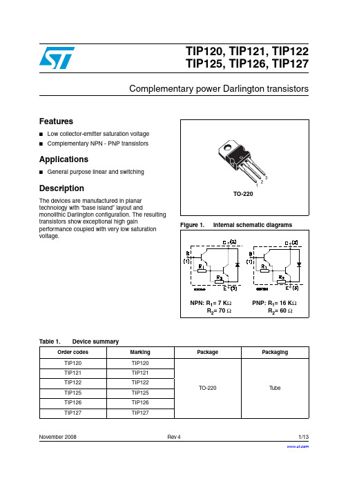
Darlington Transistors TIP120, TIP121, TIP122
Characteristics (Tj = 25°C) Min. Emitter-Base cutoff current – Emitterreststrom IC = 0, VEB = 5 V IC = 3 A, IB = 12 mA IC = 5 A, IB = 20 mA IC = 3 A, VCE = 3 V VCE = 3 V, IC = 0.5 A VCE = 3 V, IC = 3 A VCE = 4 V, IC = 3 A, f = 1 MHz VCB = 10 V, IE = ie = 0, f = 100 kHz Thermal resistance – Wärmewiderstand junction to ambient air – Sperrschicht zu umgebender Luft junction to case – Sperrschicht zu Gehäuse Admissible torque for mounting Zulässiges Anzugsdrehmoment Recommended complementary PNP transistors Empfohlene komplementäre PNP-Transistoren Equivalent Circuit – Ersatzschaltbild IEB0 VCEsat VCEsat VBEon hFE hFE hfe CCB0 – – – – 1000 1000 4 –
Kennwerte (Tj = 25°C) Typ. – – – – – – – – RthA RthC M4 Max. 2 mA 2V 4V 2.5 V – – – 200 pF 62.5 K/W 2) 2 K/W 9 ± 10% lb.in. 1 ± 10% Nm
TIP135中文资料

TIP135, TIP136, TIP137PNP SILICON POWER DARLINGTONSJUNE 1973 - REVISED MARCH 1997NOTES:5.These parameters must be measured using pulse techniques, t p = 300 µs, duty cycle ≤ 2%.6.These parameters must be measured using voltage-sensing contacts, separate from the current carrying contacts.electrical characteristics at 25°C case temperaturePARAMETERTEST CONDITIONSMIN TYPMAXUNITV (BR)CEOCollector-emitter breakdown voltage I C = -30 mA I B = 0(see Note 5)TIP135TIP136TIP137-60-80-100VI CEOCollector-emitter cut-off currentV CE = -30 V V CE = -40 V V CE = -50 V I B =0I B =0I B =0TIP135TIP136TIP137-0.5-0.5-0.5mA I CBOCollector cut-off currentV CB = -60 V V CB = -80 VV CB =-100 V V CB = -60 V V CB = -80 V V CB =-100 VI E =0I E =0I E =0I E =0I E =0I E =0T C = 100°C T C = 100°C T C = 100°CTIP135TIP136TIP137TIP135TIP136TIP137-0.2-0.2-0.2-1-1-1mA I EBO Emitter cut-off current V EB = -5 V I C =0-5mA h FE Forward current transfer ratio V CE = -4 V V CE = -4 V I C =-1A I C =-4A (see Notes 5 and 6)500100015000V CE(sat)Collector-emitter saturation voltage I B = -16 mA I B = -30 mA I C =-4A I C =-6A (see Notes 5 and 6)-2-3V V BE Base-emitter voltageV CE = -4 V I C = -4 A (see Notes 5 and 6)-2.5V C obo Output capacitance V CB = -10 V I E =0200pF V ECParallel diode forward voltageI E = -8 AI B =0(see Notes 5 and 6)-3.5Vthermal characteristicsPARAMETERMINTYPMAX UNIT R θJC Junction to case thermal resistance 1.78°C/W R θJAJunction to free air thermal resistance62.5°C/WMAXIMUM SAFE OPERATING REGIONSTHERMAL INFORMATIONMECHANICAL DATATO-2203-pin plastic flange-mount packageThis single-in-line package consists of a circuit mounted on a lead frame and encapsulated within a plastic compound. The compound will withstand soldering temperature with no deformation, and circuit performance characteristics will remain stable when operated in high humidity conditions. Leads require no additional cleaning or processing when used in soldered assembly.IMPORTANT NOTICEPower Innovations Limited (PI) reserves the right to make changes to its products or to discontinue any semiconductor product or service without notice, and advises its customers to verify, before placing orders, that the information being relied on is current.PI warrants performance of its semiconductor products to the specifications applicable at the time of sale in accordance with PI's standard warranty. Testing and other quality control techniques are utilized to the extent PI deems necessary to support this warranty. Specific testing of all parameters of each device is not necessarily performed, except as mandated by government requirements.PI accepts no liability for applications assistance, customer product design, software performance, or infringement of patents or services described herein. Nor is any license, either express or implied, granted under any patent right, copyright, design right, or other intellectual property right of PI covering or relating to any combination, machine, or process in which such semiconductor products or services might be or are used.PI SEMICONDUCTOR PRODUCTS ARE NOT DESIGNED, INTENDED, AUTHORIZED, OR WARRANTED TO BE SUIT ABLE FOR USE IN LIFE-SUPPORT APPLICA TIONS, DEVICES OR SYSTEMS.Copyright © 1997, Power Innovations Limited。
FSP3 FSP7 FSP13 FSP30 FSP40指示书说明书

S p e c i f i c a t i o nsSpectrum Analyzer ¸FSPSpecificationsSpecificationsSpecifications are valid under the following conditions:15 minutes warm-up time at ambient temperature, specified environmental conditions met, calibration cycle adhered to, and total calibration performed.Data without tolerances: typical values only.Data designated "nominal" applies to design parameters and is not tested.Data designated "σ = xx dB" is shown as standard deviation.¸FSP3¸FSP7¸FSP13¸FSP30¸FSP40 FrequencyFrequency range9 kHz to 3GHz9 kHz to 7GHz9 kHz to 13.6GHz9 kHz to 30GHz9 kHz to 40GHz Frequency resolution0.01 HzInternal reference frequency (nominal)Aging per year1)1)After 30 days of operation.1 × 10–6Temperature drift 1 × 10⁻⁶With option ¸FSP-B4 (OCXO)Aging per year1) 1 × 10⁻⁷Temperature drift 1 × 10⁻⁸External reference frequency10 MHzFrequency display with marker or frequency counterMarker resolution span/500Max. deviation(sweep time >3× auto sweep time)±(frequency × reference frequency + 0.5% × span + 10% × resolution bandwidth + ½ (last digit)) Frequency counter resolution0.1 Hz to 10 kHz (selectable)Count accuracy (S/N >25 dB)±(frequency × reference frequency + ½ (last digit))Frequency span0 Hz,10 Hz to 3GHz0 Hz,10 Hz to 7GHz0 Hz,10 Hz to 13.6GHz0 Hz,10 Hz to 30GHz0 Hz,10 Hz to 40GHzMax. span deviation0.1% Spectral purity (dBc (1 Hz)) SSB phase noise, f = 500 MHz, for f > 500 MHz see diagrams belowCarrier offset100 Hz<–84, typ.–90 1 kHz<−100, typ.−108 10 kHz<−106, typ. −113100 kHz2)2)Valid for span >100 kHz.<−110, typ. −1131 MHz2)<−120, typ.−125 10 MHz typ.−145 Residual FMf = 500 MHz, RBW 1 kHz,sweep time 100 mstyp. 3 Hz2 Spectrum Analyzer ¸FSPSpectrum Analyzer ¸FSP3Sweep timeSpan ≥10 Hz 2.5 ms to 16000 sMax. deviation1%Span 0 Hz 1 µs to 16000 sResolution125 nsResolution bandwidthsBandwidths10 Hz to 10 MHz (–3 dB) in 1, 3 sequenceEMI bandwidths200 Hz, 9 kHz, 120 kHz (–6 dB)Bandwidth accuracy≤100 kHz<3%300 kHz to 3 MHz<10%10 MHz+10%, –30%Shape factor –60 dB: –3 dB≤100 kHz<5:1 (Gaussian filters)300 kHz to 3 MHz<15:1 (4-pole synchronously tuned filters)10 MHz<7:1Shape factor –60 dB: –6 dBEMI bandwidths<5:1Video bandwidths 1 Hz to 10 MHz in 1, 3 sequenceFFT filterBandwidths 1 Hz to 30 kHz (–3 dB) in 1, 3 sequenceBandwidth accuracy5%, nominalShape factor –60dB:–3 dB 2.5:1 nominalChannel filterBandwidths100; 200; 300; 500 Hz;1; 1.5; 2; 2.4; 2.7; 3; 3.4; 4; 4.5; 5; 6; 8.5; 9; 10; 12.5; 14; 15; 16; 18 (RRC); 20; 21; 24.3 (RRC); 25; 30; 50; 100;150; 192; 200; 300; 500 kHz; 1;1.228; 1.5; 2; 3; 5 MHz1.28 (RRC), 3.84 (RRC), 4.096 (RRC)LevelDisplay range displayed average noise level to 30 dBmMaximum input levelDC voltage50 V0 VRF attenuation 0 dBCW RF power20 dBmPulse spectral density97 dBµV (1 MHz)RF attenuation ≥10 dBCW RF power30 dBmMax. pulse voltage150 V50 VMax. pulse energy (10 µs) 1 mWs0.5 mWs1 dB compression of input mixer0 dB RF attenuation, f > 200 MHz0 dBm nominalIntermodulation3rd-order intermodulationIntermodulation-free dynamic range, level 2 × –30 dBm, ∆f > 5 × RBW or 10 kHz, whichever is larger20 MHz to 200 MHz>70 dBc, TOI >5 dBm200 MHz to 3 GHz>74 dBc, TOI >7 dBm (typ. 10 dBm)3 GHz to 7 GHz−>80 dBc, TOI >10 dBm (typ. 15 dBm)7 GHz to 13.6 GHz−−>80 dBc, TOI >10 dBm13.6 GHz to 30 GHz−−−>76 dBc, TOI >8dBm>80 dBc, TOI >10 dBm 30 GHz to 40 GHz−−−−>80 dBc, TOI >10 dBm With optional Electronic Attenuator ¸FSP-B25 switched on20 MHz to 200 MHz>74 dBc, TOI > 7 dBm−200 MHz to 3 GHz>80 dBc, TOI > 10 dBm−3 GHz to 7 GHz>84 dBc, TOI > 12 dBm−4 Spectrum Analyzer ¸FSPSecond harmonic intercept point (SHI)<100 MHz typ. 25 dBm100 MHz to 1.5 GHz typ. 35 dBm1.5 GHz to 7 GHz−typ. 80 dBm7 GHz to 13.6 GHz−−typ. 80 dBm13.6 GHz to 30 GHz−−−typ. 80 dBm30 GHz to 40 GHz−−−−typ.80 dBm Displayed average noise level(0 dB RF attenuation, RBW 10 Hz, VBW 1 Hz, 20 averages, trace average, span 0 Hz, termination 50 Ω)Frequency9 kHz<−95 dBm100 kHz<−100 dBm1 MHz<−120 dBm, typ. −125 dBm10 MHz to 1 GHz<−142 dBm,typ.−145 dBm<−140 dBm, typ. −145 dBm1 GHz to 3 GHz<−140 dBm,typ. −145 dBm<−138 dBm, typ. −143 dBm3 GHz to 7 GHz−<−138 dBm,typ. −143 dBm<−135 dBm, typ. −140 dBm7 GHz to 13.6 GHz−−<−132 dBm, typ. −138 dBm13.6 GHz to 22 GHz−−−<−120 dBm,typ. −128 dBm−22 GHz to 30 GHz−−−<−115 dBm,typ. −123 dBm−13.6 GHz to 20 GHz−−−−<−120 dBm,typ. −128 dBm 20 GHz to 30 GHz−−−−<−120 dBm,typ. −128 dBm 30 GHz to 40 GHz−−−−<−112 dBm,typ. −120 dBm Displayed average noise level with preamplifier on (option ¸FSP-B25)10 MHz to 2 GHz<–152 dBm−2 GHz to 7 GHz<–150 dBm−Immunity to interferenceImage frequency>70 dBIntermediate frequency (f <3 GHz)>70 dBSpurious responses (f >1 MHz, withoutinput signal, 0 dB attenuation)<−103 dBmOther spurious (with input signal, mixer level <–10 dBm, ∆f >100kHz)f <7 GHz: <−70 dBc f <13.6 GHz: <−64 dBc f <30 GHz: <−56 dBcLevel displayScreen501 × 400 pixels (one diagram), max. two diagrams with independent settingsLogarithmic level scale10 dB to 200 dB, in steps of 10 dBLinear level scale10% of reference level per level division (10 divisions)Traces max. 3, with two diagrams on screen max. 3 per diagramTrace detector max peak, min peak, auto peak, sample, quasi-peak, average, RMSTrace functions clear/write, max. hold, min hold, averageNumber of test points501, selectable in steps of approx. factor 2, 125 to 8001Setting range of reference levelLogarithmic level display–130 dBm to 30 dBm, in steps of 0.1 dBLinear level display70.71 nV to 7.07 V in steps of 1%Units of level scale dBm, dBmV, dBµV, dBµA, dBpW (log level display), mV, µV, mA, µA, pW, nW (linear level display)Max. uncertainty of level measurementAt 128 MHz, −30 dBm (RF attenuation10dB, RBW 10kHz, ref. level –20 dBm)<0.2 dB (σ = 0.07 dB)Spectrum Analyzer ¸FSP5Frequency response<50 kHz <+0.5/− 1.0 dB50 kHz to 3 GHz<0.5 dB (σ = 0.17 dB)3 GHz to 7 GHz–<2 dB(σ = 0.7 dB)7 GHz to 13.6 GHz––<2.5 dB1)13.6 GHz to 30 GHz–––<3 dB1)30 GHz to 40 GHz––––<4 dB1) Frequency response with option ¸FSP-B25 switched on (preamplifier, electronic attenuator)10 MHz to 3 GHz<1 dB(σ = 0.33 dB)–3 GHz to 7 GHz–<2 dB(σ = 0.7 dB)–Attenuator<0.2 dB (σ = 0.07 dB)Reference level switching<0.2 dB (σ = 0.07 dB)Display nonlinearity LOG/LIN (S/N >16 dB)RBW ≤100 kHz0 dB to –70 dB<0.2 dB (σ = 0.07 dB)–70 dB to –90 dB<0.5 dB (σ = 0.17 dB)RBW ≥300 kHz0 dB to –50 dB<0.2 dB (σ = 0.07 dB)–50 dB to –70 dB<0.5 dB (σ = 0.17 dB)Bandwidth switching uncertainty (ref. to RBW = 10 kHz)10 Hz to 100 kHz <0.1 dB (σ = 0.03 dB)300 kHz to 10 MHz<0.2 dB (σ = 0.07 dB)1 Hz to 3 kHz, FFT<0.2 dB (σ = 0.03 dB)Total measurement uncertainty0 GHz to 3 GHz0.5 dBTrigger functionsTriggerSpan ≥10 HzTrigger source free run, video, external, IF levelTrigger offset125 ns to 100 s, resolution 125 ns min. (or 1% of offset)Span = 0 HzTrigger source free run, video, external, IF levelTrigger offset±125 ns to 100 s, min. resolution 125 ns, dependent on sweep timeMax. deviation of trigger offset±(125 ns + (0.1% × delay time))Gated sweepTrigger source external, IF level, videoGate delay 1 µs to 100 sGate length125 ns to 100 s, min. resolution 125 ns or 1% of gate lengthMax. deviation of gate length±(125 ns + (0.05% × gate length))Inputs and outputs (front panel)RF input N female, 50 Ωtest port system 50 Ω,N female,3.5 mm female2)test port system 50 Ω,N female,K female2)VSWR (RF attenuation >0 dB)f <3 GHz 1.5:1f <7 GHz− 2.0:1f <13 GHz−− 2.5:1f <30 GHz−−− 3.0:1f <40 GHz−−−− 3.0:1 Input attenuator0 dB to 70 dB in 10 dB stepsWith option ¸FSP-B250 dB to 75 dB in 5 dB steps not availableProbe power supply+15 V DC, –12.6 V DC and ground, max. 150 mAKeyboard connector PS/2 female for MF2 keyboardAF output (only with option ¸FSP-B3) 3.5 mm mini-jackOutput impedance10 ΩOpen-circuit voltage up to 1.5 V, adjustable6 Spectrum Analyzer ¸FSPInputs and outputs (rear panel)IF 20.4 MHz Z out= 50 Ω, BNC femaleLevelRBW ≤30 kHz, FFT–10 dBm at reference level, mixer level >–60 dBmRBW ≥100 kHz0 dBm at reference level, mixer level >–60 dBmReference frequencyOutput BNC femaleOutput frequency10 MHzLevel 0 dBm, nominalInput10 MHzRequired level0 dBm into 50 ΩOthersPower supply for noise source BNC female, 0 V and 28 V, switchable, max. 100mAExternal trigger/gate input BNC female, >10 kΩTrigger voltage 1.4 V (TTL)IEC/IEEE bus remote control interface to IEC 625-2 (IEEE 488.2)Command set SCPI 1997.0Connector24-pin Amphenol femaleInterface functions SH1, AH1, T6, L4, SR1, RL1, PP1, DC1, DT1, C0Serial interface RS-232-C (COM), 9-pin sub-D connectorPrinter interface parallel (Centronics-compatible)Mouse connector PS/2 femaleConnector for ext. monitor (VGA)15-pin sub-D connectorGeneral dataDisplay21 cm TFT colour display (8.4”)Resolution640 × 480 pixels (VGA resolution)Pixel failure rate<2 × 10 –5Mass memory 1.44 MByte 3½” disk drive (built-in), hard diskData storage>500 instrument settings and tracesTemperaturesOperating temperature range+5°C to +40°CPermissible temperature range+5°C to +45°CStorage temperature range–40°C to +70°CDamp heat+40°C at 95% relative humidity (EN 60068-2-30)Mechanical resistanceVibration, sinusoidal 5 Hz to 150 Hz, max. 2 g at 55 Hz; 0.5 g from 55 Hz to 150 Hz; meets EN60068-2-6, EN60068-2-30, EN61010-1,MIL-T-28800D, class 5Vibration, random10 Hz to 100 Hz, acceleration 1 g (rms)Shock test40 g shock spectrum, meets MIL-STD-810C and MIL-T-28800D, classes 3 and 5Recommended calibration interval 2 years for operation with external reference,1 year with internal referencePower supplyAC supply100 V AC to 240 V AC, 50 Hz to 400Hz, 3.1 A to 1.3 A, class of protection I to VDE411Typical power consumption70 VA 120 VA150 VASafety meets EN61010-1, UL3111-1, CSAC22.2 No. 1010-1,RFI suppression meets EMC Directive of EU (89/336/EEC) and German EMC lawTest mark VDE, GS, CSA, CSA-NRTL/CDimensions in mm (W × H × D)412 × 197 × 417Weight10.5 kg11.3 kg12 kg1)RF attenuation 10 dB, sweep time >1s/1 GHz.2)See recommended extras for alternate connectors.Spectrum Analyzer ¸FSP7Specifications of optionsTracking Generator ¸FSP-B9Unless specified otherwise, specifications not valid for frequency range from –3 × RBW to +3 × RBW; however, at least not valid from –9 kHz to +9 kHz.The specified level accuracy of the tracking generator is valid under the following conditions: RF attenuation ≥ 20 dB and sweep time ≥2000 ms.FrequencyFrequency range9 kHz to 3 GHzFrequency offsetSetting range±150 MHzResolution 1 HzSpectral purity (dBc (1 Hz)) SSB phase noise, f = 500 MHz, carrier offset 100 kHzNormal mode typ. –90With FM modulation on typ. –70LevelLevel setting range–30 dBm to 0 dBm in steps of 0.1 dBLevel setting range with AM–30 dBm to –6 dBm in steps of 0.1 dBMax. deviation of output level, 128 MHz, 0 dBm<1 dBFrequency responseOutput level 0 dBm, 100 kHz to 2 GHz<1 dBOutput level 0 dBm to −25 dBm, 9 kHz to 3 GHz<3 dBDynamic rangeAttenuation measurement range, RBW = 1 kHz, f > 10 MHz120 dBSpuriousHarmonics, output level –10 dBm typ. –30 dBcNonharmonics, output level 0 dBm typ. –30 dBcModulationModulation format (external)I/Q, AM, FM, FM-DC, PM, ASK, FSKAM, f > 10 MHzModulation depth0% to 99%Modulation frequency range0 Hz to 1 MHzFM, f > 10 MHzFrequency deviation0 Hz to 20 MHzModulation frequency range0 Hz to 100 kHzI/Q modulation, f > 10 MHz0 Hz to 30 MHz typ. 1 dBInputs and outputs (front panel)RF output N female, 50 ΩVSWR typ. 2:1Inputs and outputs (rear panel)TG/AM IN V max(pp) = 1 V; Z in = 50 Ω, BNC femaleTG Q/FM IN V max(pp) = 1 V; Z in = 50 Ω, BNC femaleExternal Generator Control ¸FSP-B10Supported signal generators¸SME02/03/06, ¸SMG, ¸SMGL, ¸SMGU, ¸SMH, ¸SMHU,¸SMIQ02B/02E/03B/03E/04B/06B¸SML, ¸SMR20/27/30/40/60¸SMP02/22/03/04,¸SMX, ¸SMY¸SMT02/03/06LAN Interface ¸FSP-B16Connector (rear panel)RJ-45Supported protocols10Base-T (IEEE standard 10 Mbit/s 802.3)100Base-TX (IEEE standard 100 Mbit/s 802.3u)Extended Environmental Specification ¸FSP-B20Temperature range (noncondensing)Operating temperature range 0°C to +50°CPermissible temperature range0°C to +55°CMechanical resistanceVibration, random10 Hz to 300 Hz, acceleration 1.9 g (rms)8 Spectrum Analyzer ¸FSPLO/IF ports for external Mixers ¸FSP-B21 (¸FSP40 only)LO levelFrequency range 7 GHz to 13.2 GHzLevel+15.5 dBm ±3 dBIF inputIF frequency 404.4 MHzFull scale level2 port mixer, LO output/IF input (front) –20 dBmLevel deviation<1dBIF level –30 dBm, reference level –20 dBm, RBW 30 kHz,LO output/IF input (front)Full scale level3 port mixer, IF input (front) –20 dBmLevel deviationIF level –30 dBm, reference level –20 dBm, RBW 30 kHz, IF input (front)<1dBInputs and outputs (front)LO output/IF input SMA female, 50 ΩIF input SMA female, 50 ΩElectronic Attenuator ¸FSP-B25 (only for ¸FSP3 and ¸FSP7)FrequencyFrequency range10 MHz to 7 GHzInput attenuator range (mechanical)0 dB to 75 dB in 5 dB stepsElectronic attenuation range0 dB to 30 dB in 5 dB stepsPreamplifier20 dB, switchableDisplayed average noise level with preamplifier on (0 dB RF attenuation, RBW 10 Hz, VBW 1 Hz, 20 averages, trace average, span 0 Hz, termination 50 Ω) 10 MHz to 2 GHz<–152 dBm2 GHz to 7 GHz<–150 dBmIntermodulation with electronic attenuator on3rd-order intermodulation, intermodulation-free dynamic range, level 2 × –30 dBm, ∆f >5 × RBW or 10 kHz, whichever is larger20 MHz to 200 MHz>74 dBc, TOI >7 dBm200 MHz to 3 GHz>80 dBc, TOI >10 dBm3 GHz to 7 GHz>84 dBc, TOI >12 dBmMax. deviation of level measurement<0.2 dB (σ = 0.07 dB)128 MHz, –30 dBm (RF attenuation 10 dB, RBW 10 kHz,ref. level –20dBm), preamplifier onElectronic attenuator<0.2 dB (σ = 0.07 dB)Frequency response with preamplifier, electronic attenuator10 MHz to 3 GHz<1.0 dB (σ = 0.33 dB)3 GHz to 7 GHz<2 dB (σ = 0.7 dB)Trigger Port ¸FSP-B28Output voltage high ≤1.4 Vlow ≥0.7 VTrigger port connector25-pin sub-D femaleFrequency range extension 20 Hz ¸FSP-B29Frequency range 20 Hz to f maxFrequency response <9 kHz <1 dBDisplayed average noise level0 dB RF attenuation, RBW 10 Hz, VBW 1 Hz, 20 averages, trace average, span 0 Hz, termination50Ω20 Hz<–58 dBm100 Hz<–75 dBm1 kHz<–85 dBmDC Power Supply ¸FSP-B30Input voltage range10 V to 28 V DC25 A to 12.5 AOutput voltage 120 V to 360 V DC/300 WCurrent consumption (V DC = 12 V, ¸FSP without options, default settings)¸FSP3typ. 6 A¸FSP30typ. 8 AOperating temperature range 0°C to +50°CStorage temperature range–40°C to +70°CDimensions in mm (W × H × D)145 × 154 × 65Weight0.6 kgSpectrum Analyzer ¸FSP9Battery Pack ¸FSP-B31/-B32NiMH battery pack with built-in load control for all ¸FSP and ¸ESPI models with options ¸FSP-B1 and ¸FSP-B30Input voltage of battery pack10 V to 28 V DCInput voltage power supply (battery charge)24 V DC/max. 3 AOutput voltageBattery operation13.2 V DC/200 WhBypass operation10 V to 28 V DC/10 ATypical operating times (¸FSP without options)¸FSP3 2 h¸FSP30 1.5 hCharging time 5 h at 25°COperating temperature range (discharging)0°C to +50°COperating temperature range (charging)+10°C to +40°CStorage temperature range (<1 year)–20°C to +35°CStorage temperature range (<1 month)–20°C to +55°CDimensions (W × H × D)400 mm × 134 mm × 42 mmWeight 3.7 kgAC adapter (¸FSP-B31 only)Input voltage range100 V to 240 V AC ±10%Input frequency range50 Hz to 60 Hz ±5%Input power140 VAOutput voltage24 VOutput current 3 AOperating temperature range 0°C to +50°CStorage temperature range –20°C to +70°CDimensions (W × H × D)132 mm × 58 mm × 30 mmWeight0.3 kgOrdering informationOrder designation Type Order No. Spectrum Analyzer, 9 kHz to 3 GHz¸FSP31164.4391.03 Spectrum Analyzer, 9 kHz to 7 GHz¸FSP71164.4391.07 Spectrum Analyzer, 9 kHz to 13.6 GHz¸FSP131164.4391.13 Spectrum Analyzer, 9 kHz to 30 GHz¸FSP301164.4391.30 Spectrum Analyzer, 9 kHz to 40 GHz¸FSP401164.4391.40 Accessories suppliedPower cable, compact manual, CD-ROM with operating manual and service manual.¸FSP30: test port adapter with 3.5 mm female (1021.0512.00) and N female (1021.0535.00) connector.¸FSP40: test port adapter with K female (1036.4770.00) and N female (1036.4777.00) connector.OptionsOrder designation Type Order No.Retrofittable RemarksOptionsDelete Manuals¸FSP-B01129.8394.02Rugged Case, carrying handle (factory-fitted)¸FSP-B11129.7998.02noAM/FM Audio Demodulator¸FSP-B31129.6491.02yes not with ¸FSP-B15. OCXO Reference Frequency ¸FSP-B41129.6740.02yesTV Trigger/RF Power Trigger¸FSP-B61129.859.4.02yes not with ¸FSP-B21. Internal Tracking Generator 9 kHz to 3GHz, I/Q modulator, for all ¸FSP models¸FSP-B91129.6991.02yesExternal Generator Control for all ¸FSP models¸FSP-B101129.7246.02yesPulse Calibrator for ¸FSP¸FSP-B151155.1006.02yes not with ¸FSP-B3;required for ¸FS-K72/-K73 LAN Interface 100BT for all ¸FSP models with Windows XP (1164.4391.xx)¸FSP-B161129.8042.03yes10 Spectrum Analyzer ¸FSPOrder designation Type Order No.Retrofittable RemarksLAN Interface 100BT for all ¸FSP models with Windows NT (1043.4495.xx)¸FSP-B161129.8042.02yesExtended Environmental Specification ¸FSP-B201155.1606.06noLO/IF Ports for External Mixers¸FSU-B211157.1090.02yes not with ¸FSP-B6;only for ¸FSP40¸FSP-B251129.7746.02yesElectronic Attenuator, 0 dB to 30 dB, 5 dB steps, integrated preamplifier for¸FSP3 and ¸FSP7Trigger Port for ¸FSP for indication of trigger conditions¸FSP-B281162.9915.02yesFrequency Range Extension 20 Hz for ¸FSP3/7¸FSP-B291163.0663.07noFrequency Range Extension 20 Hz for ¸FSP13/30¸FSP-B291163.0663.30noFrequency Range Extension 20 Hz for ¸FSP40¸FSP-B291163.0663.40noDC Power Supply for Spectrum Analyzers ¸FSP¸FSP-B301155.1158.02yesBattery Pack for Spectrum Analyzers ¸FSP¸FSP-B311155.1258.02yes¸FSP-B1 and¸FSP-B30 required Spare Battery Pack for Spectrum Analyzers ¸FSP¸FSP-B321155.1506.02yes¸FSP-B31 required Demodulation Hardware and Memory Extension¸FSP-B701157.0559.02yes required for ¸FS-K72/-K73; ¸FSP-B15 required SoftwarePhase Noise Measurement Software¸FS-K41108.0088.02GSM/EDGE Application Firmware, Mobile¸FS-K51141.1496.02AM/FM/ϕM Measurement Demodulator¸FS-K71141.1796.02Application Firmware for Bluetooth® Measurements¸FS-K81157.2568.02Power Sensor Measurements¸FS-K91157.3006.02supports ¸NRP-Z11/-Z21with ¸NRP-Z4 USB con-nectorApplication Firmware for Noise Figure and Gain Measurements¸FS-K301300.6508.02Preamplifier ¸FSP-B25recommended3GPP BTS/Node B FDD Application Firmware¸FS-K721154.7000.02¸FSP-B15 and -B70required3GPP UE FDD Application Firmware¸FS-K731154.7252.02¸FSP-B15 required,¸FSP-B70 recommended 3GPP HSDPA BTS Application Firmware¸FS-K741300.7156.02¸FS-K72 required3GPP TD-SCDMA BTS Application Firmware¸FS-K761300.7291.023GPP TD-SCDMA UE Application Firmware¸FS-K771300.8100.02CDMA2000® (IS-95) 1xEV-DV BTS FDD Application Firmware¸FS-K821157.2316.02CDMA2000® 1xEV-DV MS Application Firmware¸FS-K831157.2416.02CDMA2000® 1xEV-DO BTS Application Firmware¸FS-K841157.2851.02CDMA2000®-1xEV-DO MS Application Firmware¸FS-K851300.6689.02WLAN 802.11a TX Measurements Application Firmware¸FSP-K901300.6650.02The Bluetooth word mark and logos are owned by the Bluetooth SIG, Inc. and any use of such marks by Rohde&Schwarz is under license.CDMA2000® is a registered trademark of the Telecommunications Industry Association (TIA -USA).Spectrum Analyzer ¸FSP11Europe:Tel:+491805124242,e-mail:*********************************.com·USA:Tel.+1410-910-7988,e-mail:*********************************.comAsia:Tel.+6568463710,e-mail:***********************************.com¸i s a r e g i s t e r e d t r a d e m a r k o f R o h d e &S c h w a r z G m b H &C o . K G · T r a d e n a m e s a r e t r a d e m a r k s o f t h e o w n e r s · P r i n t e d i n G e r m a n y (B i a s )P D 0758.1206.22 · S p e c t r u m A n a l y z e r ¸F S P · V e r s i o n 05.00 · O c t o b e r 2004 · D a t a w i t h o u t t o l e r a n c e l i m i t s i s n o t b i n d i n g · S u b j e c t t o c h a n g eCertified Quality System ISO 9001Certified Environmental SystemISO 14001Product brochure see PD 0758.1206.12 and at (search term: FSP)Recommended extrasDesignationTypeOrder No.Headphones 0708.9010.00US Keyboard with Trackball ¸PSP-Z21091.4100.02PS/2 Mouse¸FSE-Z21084.7043.02DC Block,10kHz to 18GHz (type N)¸FSE-Z41084.7443.02Colour Monitor, 15", 230 V ¸PMC31082.6004.02IEC/IEEE Bus Cable, 1 m ¸PCK 0292.2013.10IEC/IEEE Bus Cable, 2 m ¸PCK 0292.2013.2019" Rack Adapter (not for ¸FSP-B1)¸ZZA4781096.3248.00Soft Carrying Case, grey¸ZZT4731109.5048.00Printed operating manual (German)–1093.4820.11Printed operating manual (English)–1093.4820.12Printed service manual (German)–1093.4820.81Printed service manual (English)–1093.4820.82Matching Pads, 75 ΩL Section¸RAM 0358.5414.02Series Resistor, 25 Ω1)1)Taken into account in device function RF INPUT 75 Ω.¸RAZ 0358.5714.02SWR Bridge, 5 MHz to 3 GHz ¸ZRB2 0373.9017.52SWR Bridge, 40 kHz to 4 GHz ¸ZRC 1039.9492.52High-Power Attenuators, 100 W 3/6/10/20/30 dB¸RBU1001073.8495.XX (XX=03/06/10/20/30)High-Power Attenuators, 50 W 3/6/10/20/30 dB ¸RBU501073.8695.XX (XX=03/06/10/20/30)For ¸FSP30Test Port Adapter, 3.5 mm male –1021.0529.00Test Port Adapter, N male–1021.0541.00Microwave Measurement Cable and Adapter Set ¸FS-Z151046.2002.02For ¸FSP40Test Port Adapter K male –1036.4802.00Test Port Adapter N male –1036.4783.00Test Port Adapter 2.4 mm female¸FSE-Z51088.1627.02Related data sheetsTitleOrder No.TV Trigger/RF Power Trigger ¸FSP-B6PD 0757.6433Noise Measurement Software ¸FS-K3 for Spectrum Analyzers ¸FSE, ¸FSIQ and ¸FSP PD 0757.2380Phase Noise Measurement Software ¸FSE-K4PD 0757.6727GSM/EDGE Application Firmware ¸FS-K5 for ¸FSP PD 0757.6185FM Measurement Demodulator ¸FS-K7 PD 0757.6685Bluetooth Application Firmware ¸FS-K8PD 0757.7730Application Firmware for Noise Figure and Amplifier Measure-ments R&S®FS-K30PD 0758.0839.32WCDMA 3GPP Application Firmware ¸FS-K72/-K73/-K74 PD 0757.7246TD-SCDMA Test Application Firmware ¸FS-K76/-K77 PD 0758.0880.32CDMA2000® Base Station Test Application Firmware 1xEV-DO Base Station Test Application Firmware ¸FS-K82/-K84PD 0758.1712.32Mobile Station Test Application Firmware ¸FS-K83/¸FS-K85PD 0758.1729.32WLAN Application Firmwar e ¸FSQ-K91/ ¸FSP-K90PD 0758.1435.12。
TIP132中文资料

TIP132TIP135TIP137COMPLEMENTARY SILICON POWERDARLINGTON TRANSISTORSsSTMicroelectronics PREFERRED SALESTYPESAPPLICATIONs LINEAR AND SWITCHING INDUSTRIAL EQUIPMENTDESCRIPTIONThe TIP132is a silicon Epitaxial-Base NPN power transistor in monolithic Darlington configuration,mounted in Jedec TO-220plastic package.It is intented for use in power linear and switching applications.The complementary PNP type is TIP137.Also TIP135is a PNP type.®INTERNAL SCHEMATIC DIAGRAMOctober 1999ABSOLUTE MAXIMUM RATINGSSymbolParameterValueUnitNPN TIP132PNPTIP135TIP137V CBO Collector-Base Voltage (I E =0)60100V V CEO Collector-Emitter Voltage (I B =0)60100V V EBO Emitter-Base Voltage (I C =0)5V I C Collector Current 8A I CM Collector Peak Current 12A I B Base Current0.3A P tot Total Dissipation at T cas e ≤ 25 o CT amb ≤ 25 o C702W WT s tg Storage Temperature-65to 150o C T jMax.Operating Junction Temperature150oC*For PNP types voltage and current values are negative.R 1Typ.=5K ΩR 2Typ.=150Ω123TO-2201/4THERMAL DATAR thj-case R thj-amb Thermal Resistance Junction-case MaxThermal Resistance Junction-ambient Max1.7863.5o C/Wo C/WELECTRICAL CHARACTERISTICS(T case=25o C unless otherwise specified)Symbol Parameter Test Conditions Min.Typ.Max.UnitI CEO Collector Cut-offCurrent(I B=0)V CE=Half Rated V CEO0.5mAI CBO Collector Cut-offCurrent(I E=0)V CB=Rated V CBO0.2mAI EBO Emitter Cut-off Current(I C=0)V EB=5V5mAV CEO(sus)*Collector-EmitterSustaining Voltage(I B=0)I C=30mAfor TIP135for TIP132/TIP13760100VVV CE(sat)*Collector-EmitterSaturation Voltage I C=4A I B=16mAI C=6A I B=30mA24VVV BE*Base-Emitter Voltage I C=4A V CE=4V 2.5Vh F E*DC Current Gain I C=1A V CE=4VI C=4A V CE=4V500100015000∗ Pulsed:Pulse duration=300µs,duty cycle1.5%For PNP types voltage and current values are negative.Power Derating Curve Safe Operating AreasTIP132/TIP135/TIP1372/4DIM.mminch MIN.TYP.MAX.MIN.TYP.MAX.A 4.40 4.600.1730.181C 1.23 1.320.0480.051D 2.402.720.0940.107D1 1.270.050E 0.490.700.0190.027F 0.610.880.0240.034F1 1.14 1.700.0440.067F2 1.14 1.700.0440.067G 4.95 5.150.1940.203G1 2.4 2.70.0940.106H210.010.400.3930.409L216.40.645L413.014.00.5110.551L5 2.65 2.950.1040.116L615.2515.750.6000.620L7 6.2 6.60.2440.260L9 3.5 3.930.1370.154DIA.3.75 3.850.1470.151P011CTO-220MECHANICAL DATATIP132/TIP135/TIP1373/4TIP132/TIP135/TIP137Information furnished is believed to be accurate and reliable.However,STMicroelectronics assumes no responsibility for the consequences of use of such information nor for any infringement of patents or other rights of third parties which may result from its use.No license is granted by implication or otherwise under any patent or patent rights of STMicroelectronics.Specification mentioned in this publication are subject tochange without notice.This publication supersedes and replaces all information previously supplied.STMicroelectronics products are not authorized for use as critical components in life support devices or systems without express written approval of STMicroelectronics.The ST logo is a trademark of STMicroelectronics©1999STMicroelectronics–Printed in Italy–All Rights ReservedSTMicroelectronics GROUP OF COMPANIESAustralia-Brazil-China-Finland-France-Germany-Hong Kong-India-Italy-Japan-Malaysia-Malta-Morocco-Singapore-Spain-Sweden-Switzerland-United Kingdom-U.S.A..4/4。
6N137中文资料_数据手册_参数
万联芯城电子元器件采购网已经和国内多家终端生产研发企业 形成战略合作伙伴关系,所售电子元器件数量繁多,质量优秀, 保证原装现货库存,价格皆有优势,万联芯城为客户提供电子元 器件一站式配套报价业务,只需提交 BOM 表即可得到报价 点击进入万联芯城
பைடு நூலகம்
HCPL2631M REV. 1.0.3 8 测试电路 (续) + 5V峰 3 2 1 4 8 7 6五 GND V CC ? (V)产量 350 Ω V厘米 FF V一个乙脉冲GEN一世 F厘米 V 0V ? V 5V切换位置. (A),I = 0 F ? V(大)厘米 0.5 V ? V切换位置. (B),I = 7.5MA F H CM L V(小) ?旁路 0.1 μF图14测试电路共 模瞬变抗扰度 通道:6N137,HCPL2601,HCPL2611双通道:HCPL2630,HCPL2631高速10MBIT / S逻辑门光电耦合器特征 ■ 非常高的速度 - 10 MBIT / S ■ 卓越的CMR - 10 KV /μS ■ 双工电压-48V ■ 超出-40°C至+ 85°C范围内的8个扇出 ■ 逻辑门输出 ■ 可选择输出 ■ 有线 OR开路集电极 ■ UL认可(文件#E90700)应用 ■ 接地回路消除 ■ LSTTL到TTL,LSTTL或5伏CMOS ■ 线路接收器,数据传输 ■ 数据复用 ■ 开关电源 ■ 脉冲变压器更换 ■ 计算机外设接口描述 6N137,HCPL2601,HCPL2611单通道和 HCPL2630, HCPL2631双 通道光耦合器由一个850纳米的ALGAAS LED组成,光学耦合到A非常高速的集成光电检测器逻辑门一个可选择的输出.该输出具有开 放式集合 - 从而允许接线或输出.耦合参数在整个温度范围内保证 -40°C至+ 85°C.大输入信号为5MA提供13MA的小输出灌电流(扇 出 8).内部噪音屏蔽提供了优越的通用性通常为10KV /μS的模式抑制. HCPL2601和 HCPL2631的小CMR为5KV /μS.该 HCPL2611的小 CMR为10KV /μS.原理图包概述 8 1 8 1 8 1 引脚8和5之间必须连接一个0.1PF的旁路电容 (1) . 1 2 3 4五 6 7 8 N / C _ V CC V ? V ? GND + N / C V F 1 2 3 4五 6 7 8 + _ V F1 V CC V 01 V 02 GND V F2 _ + HCPL2631 6N137 HCPL2601 HCPL2611 真值表 (正逻辑)输入启用产量 H H大号大号 H H H大号 H大号大号 H H NC大号大号 NC H 350 Ω图9启用传播延迟与温度的关系 RL = 4 K Ω(TELH) R L = 1 K Ω(TELH) R L = 350 Ω(TELH) R L = 350 Ω R L = 1 K Ω R L = 4 K Ω (TEHL)图10切换时间与温度的关系 RL = 1 K ΩTPLH RL = 350 ΩTPLH RL = 4 K ΩTPLH RL = 1 K Ω RL = 4 K Ω RL = 350 Ω效 TPH1图11高电平输出电流与温度 V CC = 5.5 V条件: V O = 5.5V V E
TIP131;TIP131G;TIP132G;中文规格书,Datasheet资料
DUTY CYCLE, D = t1/t2
0.5 1.0 2.0
5.0 10 20
t, TIME (ms)
Figure 3. Thermal Response
50 100 200
500 1.0 k
r(t), TRANSIENT THERMAL RESISTANCE (NORMALIZED)
BASE COLLECTOR EMITTER COLLECTOR
TIP13xG AYWW
TIP13x x A Y WW G
= Device Code = 1, 2, or 7 = Assembly Location = Year = Work Week = Pb−Free Package
ORDERING INFORMATION
DARLINGTON 8 AMPERE COMPLEMENTARY SILICON
POWER TRANSISTORS 80−100 VOLTS, 70 WATTS
MARKING DIAGRAM
4
1 2 3
220AB CASE 221A
STYLE 1
STYLE 1: PIN 1. 2. 3. 4.
IB PD PD TJ, Tstg
300 70 2.0 – 65 to + 150
mAdc W W °C
THERMAL CHARACTERISTICS
Characteristic
Symbol
Max
Unit
Thermal Resistance, Junction−to−Case
RqJC
1.78
°C/W
--- 2.04
STYLE 1: PIN 1. BASE 2. COLLECTOR 3. EMITTER 4. COLLECTOR
Belimo B317 无锈钢球类型三向混合 分流阀数据表

B317•ApplicationStainless Steel Ball and StemTechnical dataFunctional dataValve Size 0.75" [20]Fluidchilled or hot water, up to 60% glycol Fluid Temp Range (water)0...250°F [-18...120°C]Body Pressure Rating 600 psi Close-off pressure ∆ps 200 psiFlow characteristic A-port equal percentage, B-port modified for constant common port flow Servicing maintenance-free Flow Pattern 3-way Mixing/Diverting Leakage rate0% for A – AB, <2.0% for B – AB Controllable flow range 75°Cv4.7 Body pressure rating note 600 psiCv Flow RatingA-port: as stated in chart B-port: 70% of A – AB Cv MaterialsValve body Nickel-plated brass body Stem seal EPDM (lubricated)SeatPTFEPipe connection NPT female ends O-ring EPDM (lubricated)Ballstainless steel Suitable actuatorsNon-SpringTR LRB(X)NRB(X) N4Safety notesWARNING: This product can expose you to lead which is known to the State of California to cause cancer and reproductive harm. For more information go to Product featuresThis valve is typically used in air handling units on heating or cooling coils, and fan coil unit heating or cooling coils. Some other common applications include Unit Ventilators, VAV box re-heat coils and bypass loops. This valve is suitable for use in a hydronic system with variable or constant flow.B317 Flow/Mounting detailsDimensionsDimensional drawingsLRB, LRXA B C D E F H1H28.5" [216] 2.7" [69] 5.8" [147] 5.1" [129] 1.3" [33] 1.5" [39] 1.2" [30]1" [25]ARB N4, ARX N4A B C D E F11.4" [289] 2.8" [70]7.7" [196]7.0" [179] 3.1" [80] 3.1" [80]LRQB, LRQXA B C D E F H1H28.9" [226] 2.7" [69] 6.3" [159] 5.6" [142] 1.6" [40] 1.6" [40] 1.2" [30] 1.3" [33]TRA B C D E F3.7" [95] 2.7" [69]4.8" [122] 4.2" [107] 1.3" [33] 1.2" [31]B317TFRB, TFRXA B C D E F6.6" [167] 2.7" [69] 4.9" [124] 4.3" [110] 1.5" [39] 1.5" [39]LFA B C D E F8.6" [218] 2.7" [69] 6.3" [159] 5.6" [142] 1.8" [46] 1.9" [48]TR24-SR US••••••Modulating, Non-Spring Return, 24 V, for DC 2...10 V or 4...20 mATechnical dataElectrical dataNominal voltageAC/DC 24 V Nominal voltage frequency 50/60 Hz Power consumption in operation 0.5 WTransformer sizing 1 VA (class 2 power source)Electrical Connection 18 GA plenum cable, 3 ft [1 m]Overload Protectionelectronic throughout full rotation Functional dataOperating range Y 2...10 VOperating range Y note 4...20 mA w/ ZG-R01 (500 Ω, 1/4 W resistor)Input Impedance 100 kΩ for 2...10 V (0.1 mA), 500 Ω for 4...20 mA Direction of motion motor selectable with switch Manual override push down handle Angle of rotation 90°Running Time (Motor)90 s / 90°Noise level, motor 35 dB(A)Position indicationMechanically, pluggable Safety dataDegree of protection IEC/EN IP40Degree of protection NEMA/UL NEMA 1 UL Enclosure Type 1Agency ListingcULus acc. to UL60730-1A/-2-14, CAN/CSAE60730-1:02, CE acc. to 2014/30/EU and 2014/35/EU; Listed to UL 2043 - suitable for use in air plenums per Section 300.22(c) of the NEC and Section 602.2 of the IMC Quality Standard ISO 9001Ambient temperature -22...122°F [-30...50°C]Storage temperature -40...176°F [-40...80°C]Ambient humidity max. 95% r.H., non-condensing Servicingmaintenance-free WeightWeight0.70 lb [0.32 kg]Safety notesCable for ZIP-RS232 US and ZIP-USB-MP US to Belimo gateways.Battery Back Up System for SY(7~10)-110120 to 24 VAC, 40 VA transformer.Cable for ZTH US to actuators w/o diagnostics socket.50% voltage divider kit (resistors with wires).PC Tool computer programming interface, serial port.Electrical installationTR24-SR USINSTALLATION NOTESProvide overload protection and disconnect as required.Actuators may also be powered by 24 VDC.Only connect common to negative (-) leg of control circuits.A 500 Ω resistor (ZG-R01) converts the 4...20 mA control signal to 2...10 V.Actuators may be connected in parallel if not mechanically linked. Power consumption and inputimpedance must be observed.Meets cULus requirements without the need of an electrical ground connection.Warning! Live Electrical Components!During installation, testing, servicing and troubleshooting of this product, it may be necessary to workwith live electrical components. Have a qualified licensed electrician or other individual who has beenproperly trained in handling live electrical components perform these tasks. Failure to follow all electricalsafety precautions when exposed to live electrical components could result in death or serious injury.2...10 V / 4...20 mA Control。
TIP122中文资料_数据手册_参数
hFE
1000 100
Tj= -40 °C Tj= 25 °C Tj=125 °C
VCE= 3 V
1000 100
Tj= -40 °C Tj= 25 °C Tj=125 °C
VCE= -3 V
10
0.01
0.1
1
Ic(A)
10
-0.01
-0.1
-1
Ic(A)
Figure 6. Collector-emitter saturation voltage Figure 7. Collector-emitter saturation voltage
TIP120, TIP121, TIP122 TIP125, TIP126, TIP127
Complementary power Darlington transistors
Features
■ Low collector-emitter saturation voltage ■ Complementary NPN - PNP transistors
Table 4. Electrical characteristics(1)
Symbol
Parameter
Test conditions
Min. Typ. Max. Unit
ICEO
Collector cut-off current (IB = 0)
for TIP120/125 for TIP121/126 for TIP122/127
for NPN type
for PNP type
VCE(sat) (V)
hFE= 250 1.4
AM00698v1
VCE(sat) (V)
hFE= 250 -1.4
APW7137BI-TRG中文资料

General Description
The APW7137 is a fixed switching frequency (1MHz typical), current-mode, step-up regulator with an integrated N-channel MOSFET. The device allows the usage of small inductors and output capacitors for portable devices. The current-mode control scheme provides fast transient response and good output voltage accuracy. The APW7137 includes under-voltage lockout, current limit, and over-temperature shutdown preventing damage in the event of an output overload.
Thermal Characteristics
Symbol θJA Parameter Junction to Ambient Thermal Resistance
(Note 2)
Typical Value SOT-23-5 260
Unit °C/W
Note 2: θJA is measured with the component mounted on a high effective thermal conductivity test board in free air. The exposed pad of package is soldered directly on the PCB.
tip127达林顿管参数
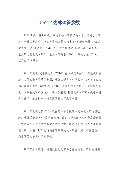
tip127达林顿管参数
TIP127是一种PNP极性的达林顿功率转换晶体管,常用于功率
放大和开关电路中。
它的参数包括最大集电极-发射极电压(VCEO)、最大集电极-基极电压(VCBO)、最大发射极-基极电压(VEBO)、
最大集电极电流(IC)、最大功率耗散(PD)、最大结温(Tj),
以及封装类型等。
最大集电极-发射极电压(VCEO)指在特定条件下,集电极和发
射极之间的最大可承受电压,通常在规格书中以伏特(V)为单位给出。
最大集电极-基极电压(VCBO)是指在特定条件下,集电极和基
极之间的最大可承受电压。
最大发射极-基极电压(VEBO)是指在特
定条件下,发射极和基极之间的最大可承受电压。
最大集电极电流(IC)是指达林顿管能够承受的最大集电极电流,通常以安培(A)为单位给出。
最大功率耗散(PD)是指晶体管
在特定条件下能够承受的最大功率耗散,通常以瓦特(W)为单位给出。
最大结温(Tj)是指晶体管的最大允许结温,超过该温度会对
晶体管的性能产生不利影响。
除了以上参数外,封装类型也是需要考虑的因素。
不同的封装
类型对于散热和安装都有不同的要求,因此在选择TIP127时,需要考虑其封装类型是否适合具体的应用场景。
总的来说,了解和理解TIP127的参数对于正确使用它,确保电路稳定可靠至关重要。
在实际应用中,需要根据具体的电路设计和要求,结合TIP127的参数来进行合理的选择和使用。
AN-136资料
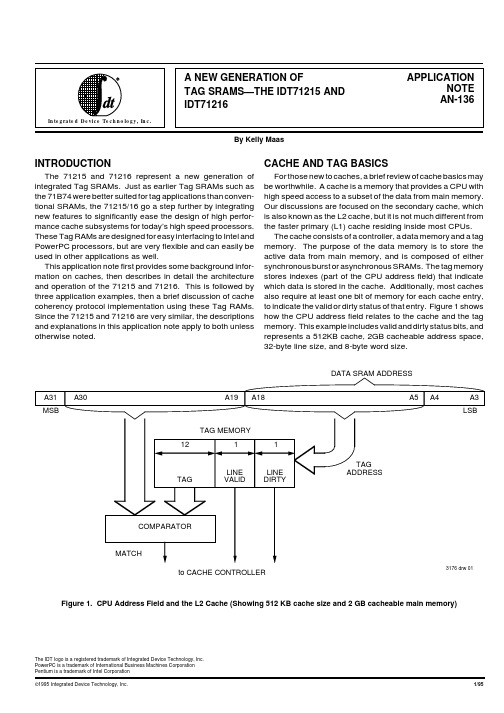
APPLICATIONNOTE AN-136A NEW GENERATION OFTAG SRAMS—THE IDT71215 AND IDT71216By Kelly MaasCACHE AND TAG BASICSFor those new to caches, a brief review of cache basics may be worthwhile. A cache is a memory that provides a CPU with high speed access to a subset of the data from main memory.Our discussions are focused on the secondary cache, which is also known as the L2 cache, but it is not much different from the faster primary (L1) cache residing inside most CPUs.The cache consists of a controller, a data memory and a tag memory. The purpose of the data memory is to store the active data from main memory, and is composed of either synchronous burst or asynchronous SRAMs. The tag memory stores indexes (part of the CPU address field) that indicate which data is stored in the cache. Additionally, most caches also require at least one bit of memory for each cache entry,to indicate the valid or dirty status of that entry. Figure 1 shows how the CPU address field relates to the cache and the tag memory. This example includes valid and dirty status bits, and represents a 512KB cache, 2GB cacheable address space,32-byte line size, and 8-byte word size.INTRODUCTIONThe 71215 and 71216 represent a new generation of integrated Tag SRAMs. Just as earlier Tag SRAMs such as the 71B74 were better suited for tag applications than conven-tional SRAMs, the 71215/16 go a step further by integrating new features to significantly ease the design of high perfor-mance cache subsystems for today’s high speed processors.These Tag RAMs are designed for easy interfacing to Intel and PowerPC processors, but are very flexible and can easily be used in other applications as well.This application note first provides some background infor-mation on caches, then describes in detail the architecture and operation of the 71215 and 71216. This is followed by three application examples, then a brief discussion of cache coherency protocol implementation using these Tag RAMs.Since the 71215 and 71216 are very similar, the descriptions and explanations in this application note apply to both unless otherwise noted.to CACHE CONTROLLER3176 drw 01Figure 1. CPU Address Field and the L2 Cache (Showing 512 KB cache size and 2 GB cacheable main memory)The IDT logo is a registered trademark of Integrated Device Technology, Inc.PowerPC is a trademark of International Business Machines Corporation Pentium is a trademark of Intel CorporationIntegrated Tag RAMs operate as ordinary SRAMs, but have an additional access mode in which a word of data (an index) is internally read (but not driven off-chip) and compared with the CPU address driven onto the Tag RAM’s data bus.Figure 2 shows the basic architecture of an integrated Tag SRAM. The comparator indicates whether the cache holds the data for the address supplied by the CPU or other bus master. This is a critical timing path since this tag “hit” or “miss”must be determined before the cache memory access can be completed (or even started, in many cases). Note that tag memories connect only to the CPU address bus and never to the CPU data bus.BASIC TAG RAM ARCHITECTUREADDRESSDATA (TAG)WRITEREAD3176 drw 02Figure 2. Basic Integrated Tag SRAM ArchitectureAn additional feature of the Tag SRAM is that a portion of the memory is resettable. This permits use of one bit of the data field as a “valid” status bit. Upon system initialization,when the cache contains random data, a quick reset will clear the valid bit for every cache line so that all initial cache accesses will result in a miss. A miss then causes the address to be loaded into the Tag RAM, data from main memory to be loaded into the data RAMs, and the valid bit to be set true. If not included in the Tag RAM, this function requires an addi-tional 1-bit wide SRAM.The reset feature of earlier Tag RAMs was sufficient for implementation of a valid bit, but nothing more. Today’s secondary caches frequently implement four-state write-back protocols such as MESI, with multiprocessor applications requiring five states (e.g. MOESI) or more. Hence, most caches need a two- or three-bit status memory that is ac-cessed separately from the tag memory. It is used in conjunc-tion with the match output to determine the response to a CPU memory access or a snoop. (A snoop is an operation initiated by the system in order to maintain coherency between the cache(s) and main memory.) This has typically been handled with yet another RAM - a conventional separate I/O SRAM organized as either x1 or x4. The 71215/16 includes a three-bit status memory on chip.THE 71215 AND 71216As shown in Figure 3, these 16K x 15 RAMs are configured internally as two memories: 16K x 12 for tag and 16K x 3 for status. These two memories share the address bus but are controlled independently. An important new feature is extra pins and logic for generating BRDY (Intel’s Burst Ready) and TA (PowerPC’s Transfer Acknowledge). These are CPU input signals which are time critical in zero wait state secondary caches. I/O’s are 3.3V compatible and there is a low power standby mode. All writes are synchronous as with burst data SRAMs, while all reads and compares are asynchronous for minimum delay. Two opposite polarity chip select pins are provided for easy depth expansion.Figure 3. Simplified 71215 / 71216 Block Diagram (71216 signal names are in parenthesis)For a 1MB cache and 4GB of cacheable main memory, two of the devices may be cascaded in depth without any timing penalty apart from increased capacitive loading. This is accomplished with the two Chip Select pins. A low order address signal may be connected to CS1 on one chip and to CS2 on the other so that at any given time, one is selected and the other is deselected. The deselected chip ignores all control inputs (except RESET and PWRDN ) and tri-states its outputs so that the two chips can be conveniently bussed together. As expected, worst case timing delays from the Chip Select inputs are the same as for the Address inputs. When only a single 71215 or 71216 is used in an application, CS1 is tied to V SS and CS2 is tied to V CC .With a 16K x 12 tag memory, the 71215 and 71216 are wider and deeper than most Tag RAMs. For a typical 64-bit CPU with a 32-byte line size, the 16K depth supports a 512KB cache while the 12-bit tag field supports 2GB of cacheable main memory. Thus, only a single component is required for most applications. Table 1 shows the relationships between Tag RAM size, cache size, and cacheable main memory size.The Tag depth is equal to the cache size divided by the line size. The Tag width is equal to the base-2 log of the ratio of main memory size to cache size.TABLE 1: REQUIRED TAG RAM SIZE AS A FUNCTION OF CACHE SIZE AND MAIN MEMORY SIZE (For 32-byte line size and directmapped cache architecture.)3176 tbl 01VLDin / S1DLYin / S2WTin / S3IN OUT OUT OUTBRDYIN W/R )3176 drw 03Figure 4. Detailed 71215 / 71216 Block Diagram (71216 pin names are in parenthesis)OUT OUT OUTBRDYOE (W/R (TA )BRDYIN (IN IN IN3176 drw 04The 71215/16 is shown in more detail in Figure 4. The tag memory is controlled by the Write Enable Tag (WET ) and Output Enable Tag (OET ) pins. During writes, WET is synchro-nous to CLK, as are the input data (TAG0 - TAG11) and address (A0 - A13). Note that WET has no effect on the TAG output buffers, so OET must be high to disable the outputs during writes. Reads are performed by deasserting WET and asynchronously asserting OET . For cache architectures in which the tag is never read (e.g. write-through caches), OET may be tied to V CC . When both WET and OET are high, the 71215/16 is in the match mode, where the TAG0 - TAG11inputs are compared with the stored data and are used to generate the MATCH and BRDY /TA outputs. In both read andmatch modes, the address path is flow-through for the fastest possible response to a new address.The three status bits of the 71215/16 are labeled VLD/S1,DTY/S2, and WT/S3. The reason for the dual names is that their functions vary, dependent on the state of the static Status Function (SFUNC) input signal. When SFUNC is low, the status bits are said to be in a “dedicated” mode and are referred to as Valid, Dirty and Write-Through. See Figure 5.When SFUNC is high, the status bits play no special role within the 71215/16 and are simply referred to as Status 1, Status 2and Status 3. See Figure 6. The functionality of VLD and WT in the dedicated mode is described later. DTY/S2 does not have any special functionality within the 71215/16.Figure 5. Dedicated Mode Logic (71216 pin names are in parenthesis)W/R BRDYOE (TAOE WT IN / S3IN DTY IN / S2VLD IN / S1OUT / S2OUT/ S1OUT(TA )BRDY IN (TAIN 3176 drw 05Figure 6. Generic Mode Logic (71216 pin names are in parenthesis)The status bits are accessed through separate input pins and output pins. This avoids the need for fast turn around on this bus as in the following example: a single word write hit to a write back line results in the need to set the state to dirty (also called “modified”). The status memory must go from reading to writing then back to reading in as little as two cycles. If common I/O is preferred, the user may tie the respective input and output pins together. The status memory control signals (WES and OES ) are equivalent to WET and OET for the tag memory. Also, because the status field is separate I/O, OES is normally tied to V SS to permanently enable the status outputs.The tag and status memories are controlled independently since normal operation of the 71215/16 finds the tag memory in match mode and the status memory in read mode. Often,however, WET and WES are tied together in a design because the write function tends to be common between them. For those times when only the status bits need to be updated,WET , WES and OET can be asserted together without havingto externally drive the TAG bus. This causes the data read from the tag field to be written back to the same address,resulting in no change to the tag data.Note that there is only one address register that is used by both memory segments. The address is registered when either WET or WES is sampled low, and is flow-through when both WET and WES are sampled high.The entire status memory is cleared to zeros when RESET is sampled low on at least one rising edge of CLK. This can be used to put the cache into a known state after power up, or after a cache flush. Since reset is a type of write, WET and WES are required to be high during reset. PWRDN must also be high, but the state of the chip select inputs does not matter.During reset, BRDY /TA is driven high, and MATCH is driven low.MATCH, BRDY AND TAAs mentioned earlier, the 71215/16 is in match mode when OET is high and WET is sampled high. This allows the TAG0BRDYOE (TAOE BRDY and Match logic (Generic Status bit mode)TA names added for ap noteWT IN / S3DTY IN / S2VLD IN / S1WT OUT / S3OUT DTY OUT / S2OUTVLD OUT / S1OUTBRDY (TA )BRDYIN (TAIN 3176 drw 06- TAG11 inputs (high order bits of the CPU/system address bus) to be compared with internally stored data. When SFUNC is low, the stored VLD bit is combined with this comparator output to generate a MATCH output that is true only when both the tag comparison is true and the VLD bit is high. Thus, an invalid tag entry does not generate a hit. Note that OES and WES do not affect internal access of the status bits. When SFUNC is high, the status bits are generic and MATCH is simply the output of the comparator. MATCH is driven low when the 71215/16 is not in match mode. When the chip is deselected, MATCH becomes high impedance.The cache/memory controller has traditionally generated the BRDY /TA signal to the CPU, using MATCH and other inputs. This is a critical timing path. During a zero-wait-state lead-off, there are only two clock cycles for the CPU to drive the address and other bus signals, and for BRDY or TA to be returned to the CPU by the cache controller. See Figure 7.Typically there is not enough time to have two chips (Tag RAM and controller) in this timing path. The 71215/16 address this difficulty by incorporating logic for generating BRDY /TA , thereby removing the cache controller from this path. This is shown in Figure 8.While the cache controller is removed from the primary BRDY /TA timing path, it must still play a part in generating BRDY /TA . The controller has address and other bus cycle information that is needed to qualify the generation of BRDY /TA . This qualification logic is best placed in parallel with the tag lookup, rather than in series with it. Also, there are cases where the the generation of BRDY /TA by the 71215/16 must be blocked so that the cache/memory controller can generate it instead.Logic has been included in the 71215/16 that enables it to qualify BRDY /TA for one particular case. While a write hit to a write-back line can be handled by the cache alone, a write-through line requires that the write also proceed to main memory. In the former case the cache can respond without wait states and BRDY /TA is driven low immediately as the result of a tag match and set VLD bit. In the latter case, main memory writes normally require wait states. If a line (or the whole cache) is write-through, the 71215/16 should not drive BRDY /TA low, so that the cache/memory controller may do so later when the main memory (or write buffer) write is complete.When the Tag RAM is in dedicated status mode (SFUNC low),the stored WT bit determines whether the line is write-through (high) or write-back (low). Note that it may also be used to denote a write protected line. Another pin - W/R and TT1 on the 71215 and 71216 respectively - connects directly to the CPU for distinguishing between processor reads and proces-sor writes. These two bits of information are used to block internal generation of BRDY /TA during a processor write to a write-through line. Without this feature, the cache controller might not have enough time to generate a blocking signal (as described below) based on the WT output from the Tag RAM.If a user wants to gate the VLD bit with MATCH but not use the WT bit in combination with W/R or TT1, he should select the dedicated mode (SFUNC low) and tie W/R low or TT1 high.Note that the one functional difference between the 71215 and 71216 is the polarity of the W/R and TT1 signals.The cache controller may have additional information and may wish to delay the assertion of BRDY /TA . Thus, the 71215and 71216 have input pins - BRDYH and TAH respectively -so that the cache controller may force BRDY /TA high, regard-less of the result of the tag comparison inside the 71215/16.In the case of a cache miss or write through, the system memory controller (usually combined with the cache control-ler) becomes completely responsible for generating BRDY or TA for that bus cycle. For flexibility, the 71215/16 incorporates two options for merging its own BRDY /TA output with that generated by the system memory controller.One approach is to bus the two signals together. This is the preferred approach when the cache (including the 71215/16)is optional, as on a module, since addition or removal of the cache does not affect the way in which the cache controller generates BRDY /TA . Figure 9 shows this approach for the 71215 used with the Pentium. It applies equally to the 71216and PowerPC. This requires that both BRDY /TA sources be tri-statable. The BRDYOE and TAOE input pins of the 71215and 71216 are driven by the cache/memory controller, and are used to enable or disable the 71215/16 BRDY /TA output as necessary. To be prepared for a possible hit, each new bus cycle begins with BRDYOE /TAOE low. In the event of a cache miss, the controller deasserts BRDYOE /TAOE , then takes over responsibility for driving BRDY /TA . This is also the procedure for writes to write-through lines, where even cache hits are responded to by the controller. Also, the controller usually takes over control of BRDY /TA for the second, third and fourth words of a burst transfer. This is required if either the CPU address is not guaranteed to remain valid throughout the entire bus cycle (a change to the 71215/16 address busFigure 8. 71215/16 BRDY/TA Timing - Chip Set Removed from the Critical PathFigure 7. Conventional Tag RAM Usage - Chip Set in BRDY/TA Critical Path 66MHz CPU 71215/16 TAGCACHE 3176 drw 0866MHz CPU TAG SRAMCACHEwill ripple through to BRDY /TA ), or if data SRAM accesses require wait states (it’s necessary to toggle BRDY /TA from cycle to cycle). For those times when neither device is driving BRDY /TA , a pull-up resistor is used to keep the signal high. In this case, it’s suggested that the controller drive BRDY /TA high before putting it in a high impedance state. Thus, the resistor is never used to generate a low to high transition and therefore can be weak (3 K Ω to 20 K Ω). Also, both the 71215/16 and controller can remain off the BRDY /TA bus for ex-tended periods of time if so desired. With this approach,BRDYIN or TAIN (Burst Ready Input, Transfer Acknowledge Input) is tied high.Figure 10. Combining BRDY/TA : Pass-Through OptionBRDY /TA functions similar to MATCH (but opposite in polarity) when the 71215/16 is not in match mode. It is high impedance when the chip is deselected (or BRDYOE /TAOE is high), and otherwise is driven high when out of match mode.REDUCED POWERFor the increasing number of applications that require a low power standby mode, the 71215/16 includes an asynchro-nous power down pin (PWRDN ). When it is driven low, both the tag and status memories are shut down to save consider-ably on power consumption. For optimum power savings, all input and bidirectional signals should also be held at CMOS voltage levels (near V CC or V SS ). During power down, all outputs are placed in a high impedance state and all data is retained. All writes should be allowed to complete before PWRDN is asserted. There is no minimum time that it must be low. When exiting the power down state, there is only a very short delay after the rising edge of PWRDN before normal activity can be resumed.SYSTEM USAGEFor applications not using the entire 12-bit tag field, the unused TAG I/O pins should be pulled either high or low through 1 K Ω to 5 K Ω resistors. For applications not using the entire 3-bit status field, the unused inputs may be tied directly to V CC or V SS , and the unused outputs are left unconnected.All other unused inputs should be tied either to V CC or V SS as appropriate for their function. This includes unused address signals ift only part of the depth of the 71215/16 is used.66MHz71215 TAG CHIP SET3176 drw 1066MHz71215 TAGCHIP SET3176 drw 09Figure 9. Combining BRDY/TA : Bussing OptionThe second approach is to have the cache/memory con-troller drive it’s BRDY /TA output into the BRDYIN /TAIN input on the 71215/16 at all times. Inside the 71215/16, BRDYIN /TAIN is registered by the clock then ANDed (negative logic ORed) with the internally generated BRDY /TA . For this approach, BRDYOE /TAOE is tied permanently low. The controller no longer generates BRDYOE /TAOE , but instead must generate BRDY /TA one cycle earlier because it is delayed by one cycle in reaching the CPU. Note that BRDYH /TAH only enables or disables the BRDY /TA generated inside the 71215/16, and does not affect the propagation of BRDYIN/TAIN through to the BRDY /TA output. Figure 10 shows this approach for the 71215 and Pentium.3176 drw 11Figure 11: Pentium / 71215 Example of 256 KB CacheWhen changing the depth of the cache (and Tag RAM), theTAG field shifts accordingly, so that it remains contiguous withthe address field. The example in Figure 11 uses only half ofa 71215, and can be compared with Figures 1 and 12. It showsa 256KB cache for the Pentium, uses the BRDY pass-throughoption from Figure 10, and maps 1GB of main memory into thecache. Two 32Kx32 burst SRAMs are shown as the cachedata RAM.3176 dr w 12Figure 12: PowerPC / 71216 Example of 512 KB CacheFigure 12 shows a 512KB cache implementation for thePowerPC, using the full address range of the 71216. Thisexample uses a bussed TA implementation shown in Figure 9.The tag size is sufficient to support 2GB of cacheable mainmemory.3176 drw 13Figure 13 shows a 1MB cache for the PowerPC using the 71216. The implementation is essentially the same as for 512KB, but with two 71216 Tags and two banks of data SRAMs. Except for CS1 and CS2, all the same signals that were connected to the first Tag RAM should be connected to the same pins of the second Tag RAM. The least significant tag bit of the 512KB cache is used to select between the two Tag RAMs of the 1MB cache. The same is true for the two banks of data SRAMs. The tag field then shifts one bit in the direction of the more significant address bits. Please note that the PowerPC and Intel processors do not have the same address sequence. A0 is the MSB for the PowerPC while A31is the MSB for Intel's processors.Figure 13: PowerPC / 71216 Example of 1 MB CacheIt is also possible to double the size of the cache and cached address space without doubling up the Tag RAMs.This can be done by doubling the line size of the cache - from 32 bytes to 64 bytes, for example. It is not necessary to have the same line size for both the primary and secondary caches,though it does simplify the cache controller. A more detailed discussion of this topic is beyond the scope of this application note.The CLK pin should be driven by the same clock that drives the CPU. Although there is no standard for clock skew tolerances between devices, a recommended target is ±1nS.MESI PROTOCOL IMPLEMENTATIONMESI is a cache coherency protocol, implemented in the primary cache of both the PowerPC 601 and the Pentium Processor. With the 71215/16, it is now practical to also implement MESI for the L2 cache. The acronym stands for Modified (write-back data that is dirty), Exclusive (clean write-back data that can later transition to Modified), Shared (write-through data which cannot become Modified) and Invalid. In short, it allows for cache lines to be individually marked aseither write-through or write-back. While the cache controller is responsible for implementing the protocol and controlling the state transitions, the 71215/16’s features can be helpful in the implementation.The following state assignments for MESI are intended to take advantage of the features of the 71215/16 when it is in the dedicated status mode (SFUNC low). Some variations are possible:TABLE 2: SUGGESTED MESI STATE AS-SIGNMENTSAs described earlier, BRDY/TA generation is blocked when VLD/S1 is low, and during write hits to write-through lines. The cache controller is responsible for all state transitions, includ-ing Exclusive to Modified.SUMMARYThe 71215 and 71216 represent a major step forward in Tag RAMs. They are sized appropriately for the majority of today’s cache and main memory requirements, and offer new features that help remove many of the barriers to the imple-mentation of zero wait-state caches.As this application note is being written, the fastest speed grade of the 71215 and 71216 is 9nS (address to match time), with faster speeds expected in the future. Please contact your local IDT sales office or representative for information on the latest speed availability.。
6N137中文详解资料
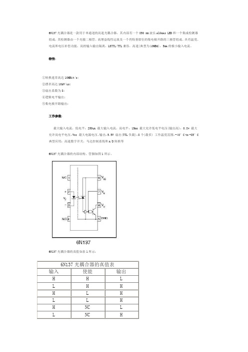
6N137光耦合器是一款用于单通道的高速光耦合器,其内部有一个850 nm波长AlGaAs LED和一个集成检测器组成,其检测器由一个光敏二极管、高增益线性运放及一个肖特基钳位的集电极开路的三极管组成。
具有温度、电流和电压补偿功能,高的输入输出隔离,LSTTL/TTL兼容,高速(典型为10MBd),5mA的极小输入电流。
特性:①转换速率高达10MBit/s;②摆率高达10kV/us;③扇出系数为8;④逻辑电平输出;⑤集电极开路输出;工作参数:最大输入电流,低电平:250uA 最大输入电流,高电平:15mA 最大允许低电平电压(输出高):0.8v 最大允许高电平电压:Vcc 最大电源电压、输出:5.5V 扇出(TTL负载):8个(最多) 工作温度范围:-40°C to +85°C 典型应用:高速数字开关,马达控制系统和A/D转换等6N137光耦合器的内部结构、管脚如图1所示。
6N137光耦合器的真值如表1所示:需要注意的是,在6N137光耦合器的电源管脚旁应有—个0.1uF的去耦电容。
在选择电容类型时,应尽量选择高频特性好的电容器,如陶瓷电容或钽电容,并且尽量靠近6N137光耦合器的电源管脚;另外,输入使能管脚在芯片内部已有上拉电阻,无需再外接上拉电阻。
6N137光耦合器的使用需要注意两点:第一是6N137光耦合器的第6脚Vo输出电路属于集电极开路电路,必须上拉一个电阻;第二是6N137光耦合器的第2脚和第3脚之间是一个LED,必须串接一个限流电阻。
6n137的内部结构原理如下图所示,信号从脚2和脚3输入,发光二极管发光,经片内光通道传到光敏二极管,反向偏置的光敏管光照后导通,经电流-电压转换后送到与门的一个输入端,与门的另一个输入为使能端,当使能端为高时与门输出高电平,经输出三极管反向后光电隔离器输出低电平。
当输入信号电流小于触发阈值或使能端为低时,输出高电平,但这个逻辑高是集电极开路的,可针对接收电路加上拉电阻或电压调整电路。
ISO 8537-2007中英文
INTERNATIONALSTANDARD 国际标准ISO8537Second edition 第2版2007-10-01Sterile single-use syringes, with or without needle, for insulin一次性无菌胰岛素注射器,带针或不带针Seringues à insuline, stériles, non réutilisables, avec ou sans aiguillePDF disclaimer 免责声明This PDF file may contain embedded typefaces. In accordance with Adobe's licensing policy, this file may be printed or viewed but shall not be edited unless the typefaces which are embedded are licensed to and installed on the computer performing the editing. In downloading this file, parties accept therein the responsibility of not infringing Adobe's licensing policy. The ISO Central Secretariat accepts no liability in this area.本PDF文件可能包含嵌入字体。
根据Adobe的许可政策,本文件可以浏览或打印,但不得修改,除非是嵌入式字体经授权并安装在电脑上方可进行编辑。
在下载这个文件,其中各方接受没有侵犯Adobe许可政策的责任。
ISO中央秘书处在这方面不承担任何责任。
713合金成分
713合金成分713合金是一种常见的高温合金,由铁、镍、钴、铬等多种金属元素组成。
这种合金具有优异的高温强度、耐腐蚀性和抗疲劳性能,广泛应用于航空航天、能源、化工等领域。
713合金的主要成分之一是铁。
铁是一种常见的金属元素,具有良好的机械性能和导电性能。
在713合金中,铁的存在增强了合金的强度和韧性。
713合金中含有大量的镍。
镍是一种具有较高熔点和良好耐腐蚀性的金属元素。
添加镍可以提高合金的耐高温性能和抗氧化性能,使得713合金在高温环境下有较好的稳定性。
713合金中还含有一定量的钴。
钴是一种贵重金属,具有优异的高温强度和抗腐蚀性能。
添加钴可以提高713合金的高温强度和耐疲劳性能,使其适用于高温、高压的工作环境。
713合金的成分中还包括铬等元素。
铬是一种耐腐蚀性极强的金属元素,可以提高713合金的抗腐蚀性能,使其在恶劣的化学环境中具有良好的耐蚀性。
713合金具有许多优异的性能。
首先,它具有出色的高温强度,可以在高温环境下保持较好的稳定性和刚性。
其次,713合金具有良好的耐蚀性,可以在酸、碱、盐等恶劣环境中长期使用。
此外,713合金还具有优异的抗疲劳性能,可以在长时间高强度工作条件下保持较好的机械性能。
713合金的应用十分广泛。
在航空航天领域,713合金常用于制造高温发动机零部件,如涡轮叶片、涡轮盘、燃烧室等。
在能源行业,713合金常用于制造燃气轮机和核电设备的关键部件,能够在高温高压的环境下工作。
此外,在化工、石油等领域,713合金也常用于制造耐腐蚀设备和管道。
713合金是一种具有优异高温强度、耐腐蚀性和抗疲劳性能的合金材料。
其成分包括铁、镍、钴、铬等多种金属元素。
713合金在航空航天、能源、化工等领域有着广泛的应用,为这些领域的发展做出了重要贡献。
通过对713合金的研究和应用,可以进一步提高材料的性能,推动相关领域的发展。
叶节点501个总结点
叶节点501个总结点
(实用版)
目录
1.阳光泰克 73 针针脚的概述
2.阳光泰克 73 针针脚的定义和功能
3.阳光泰克 73 针针脚的具体针脚定义
4.阳光泰克 73 针针脚的应用领域
正文
阳光泰克 73 针针脚是一款广泛应用于电子领域的连接器。
这款连接器拥有 73 个针脚,每个针脚都有特定的定义和功能。
阳光泰克 73 针针脚的概述:
阳光泰克 73 针针脚是一款高质量、高可靠性的连接器,它的设计紧凑,结构稳定,适用于各种恶劣环境。
它的 73 个针脚,每个针脚都承担着不同的任务,可以实现多种功能。
阳光泰克 73 针针脚的定义和功能:
阳光泰克 73 针针脚的每个针脚都有特定的定义和功能。
例如,有的针脚用于电源供电,有的针脚用于数据传输,有的针脚用于信号控制等。
这种设计使得阳光泰克 73 针针脚可以满足各种不同设备的需求,也可以实现多种功能。
阳光泰克 73 针针脚的具体针脚定义:
阳光泰克 73 针针脚的每个针脚的具体定义和功能取决于其实际应用。
一般来说,其针脚的定义和功能会根据设备的需求进行定制。
例如,如果设备需要实现数据传输功能,那么阳光泰克 73 针针脚的相应针脚就会被定义为数据传输。
阳光泰克 73 针针脚的应用领域:
阳光泰克 73 针针脚广泛应用于各种电子设备中,如计算机、通信设备、工业控制设备等。
