MA44622B中文资料
MAX4460中文资料
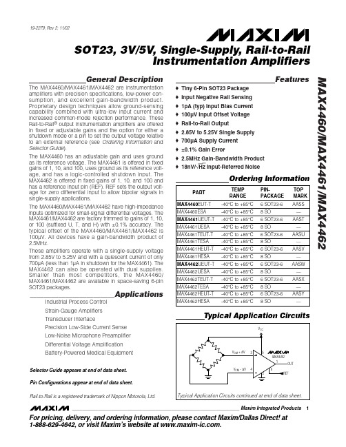
General DescriptionThe MAX4460/MAX4461/MAX4462 are instrumentation amplifiers with precision specifications, low-power con-sumption, and excellent gain-bandwidth product.Proprietary design techniques allow ground-sensing capability combined with ultra-low input current and increased common-mode rejection performance. These Rail-to-Rail ®output instrumentation amplifiers are offered in fixed or adjustable gains and the option for either a shutdown mode or a pin to set the output voltage relative to an external reference (see Ordering Information and Selector Guide ).The MAX4460 has an adjustable gain and uses ground as its reference voltage. The MAX4461 is offered in fixed gains of 1, 10, and 100, uses ground as its reference volt-age, and has a logic-controlled shutdown input. The MAX4462 is offered in fixed gains of 1, 10, and 100 and has a reference input pin (REF). REF sets the output volt-age for zero differential input to allow bipolar signals in single-supply applications.The MAX4460/MAX4461/MAX4462 have high-impedance inputs optimized for small-signal differential voltages. The MAX4461/MAX4462 are factory trimmed to gains of 1, 10,or 100 (suffixed U, T, and H) with ±0.1% accuracy. The typical offset of the MAX4460/MAX4461/MAX4462 is 100µV. All devices have a gain-bandwidth product of 2.5MHz.These amplifiers operate with a single-supply voltage from 2.85V to 5.25V and with a quiescent current of only 700µA (less than 1µA in shutdown for the MAX4461). The MAX4462 can also be operated with dual supplies.Smaller than most competitors, the MAX4460/MAX4461/MAX4462 are available in space-saving 6-pin SOT23 packages.________________________ApplicationsIndustrial Process Control Strain-Gauge Amplifiers Transducer InterfacePrecision Low-Side Current Sense Low-Noise Microphone Preamplifier Differential Voltage Amplification Battery-Powered Medical EquipmentFeatureso Tiny 6-Pin SOT23 Package o Input Negative Rail Sensing o 1pA (typ) Input Bias Current o 100µV Input Offset Voltage o Rail-to-Rail Outputo 2.85V to 5.25V Single Supply o 700µA Supply Current o ±0.1% Gain Erroro 2.5MHz Gain-Bandwidth Product o 18nV/√Hz Input-Referred NoiseMAX4460/MAX4461/MAX4462SOT23, 3V/5V , Single-Supply, Rail-to-RailInstrumentation Amplifiers________________________________________________________________Maxim Integrated Products119-2279; Rev 2; 11/02For pricing, delivery, and ordering information,please contact Maxim/Dallas Direct!at 1-888-629-4642, or visit Maxim’s website at .Ordering InformationRail-to-Rail is a registered trademark of Nippon Motorola, Ltd.Pin Configurations appear at end of data sheet.Typical Application CircuitsSelector Guide appears at end of data sheet.M A X 4460/M A X 4461/M A X 4462SOT23, 3V/5V , Single-Supply, Rail-to-Rail Instrumentation Amplifiers 2_______________________________________________________________________________________ABSOLUTE MAXIMUM RATINGSStresses beyond those listed under “Absolute Maximum Ratings” may cause permanent damage to the device. These are stress ratings only, and functional operation of the device at these or any other conditions beyond those indicated in the operational sections of the specifications is not implied. Exposure to absolute maximum rating conditions for extended periods may affect device reliability.Supply Voltage (V DD to V SS ) ...................................-0.3V to +6V All Other Pins...................................(V SS - 0.3V) to (V DD + 0.3V)Output Short-Circuit Duration to Either Supply.........................1s Continuous Power Dissipation (T A = +70°C)6-Pin SOT23 (derate 8.7mW/°C above +70°C)............695mW 8-Pin SO (derate 5.9mW/°C above +70°C)..................470mWOperating Temperature Range ...........................-40°C to +85°C Junction Temperature......................................................+150°C Storage Temperature Range.............................-65°C to +150°C Lead Temperature (soldering, 10s)....................................300°CELECTRICAL CHARACTERISTICS—MAX4460/MAX4461(V DD = 5V, V CM = 0V, V DIFF = V IN+- V IN-= 50mV to 100mV for G = 1, 20mV to 100mV for G = 10, 2mV to 48mV for G =100,MAX4460 is configured for G = 10, R L = 200k Ωto GND, T A = +25°C , unless otherwise noted.)MAX4460/MAX4461/MAX4462SOT23, 3V/5V , Single-Supply, Rail-to-RailInstrumentation AmplifiersELECTRICAL CHARACTERISTICS —MAX4460/MAX4461 (continued)ELECTRICAL CHARACTERISTICS —MAX4460/MAX4461M A X 4460/M A X 4461/M A X 4462SOT23, 3V/5V , Single-Supply, Rail-to-Rail Instrumentation Amplifiers 4_______________________________________________________________________________________ELECTRICAL CHARACTERISTICS —MAX4460/MAX4461 (continued)(V DD = 5V, V CM = 0V, V DIFF = V IN+- V IN-= 50mV to 100mV for G = 1, 20mV to 100mV for G = 10, 2mV to 48mV for G = 100,MAX4460 is configured for G = 10, R L = 200k Ωto GND, T A = T MIN to T MAX , unless otherwise noted.)MAX4460/MAX4461/MAX4462SOT23, 3V/5V , Single-Supply, Rail-to-RailInstrumentation Amplifiers_______________________________________________________________________________________5ELECTRICAL CHARACTERISTICS —MAX4462(V DD = 5V, V SS = 0V, V CM = V REF = V DD /2, R L = 100k Ωto V DD /2, T A = +25°C , unless otherwise noted. V DIFF = V IN+- V IN-= -100mVM A X 4460/M A X 4461/M A X 4462SOT23, 3V/5V , Single-Supply, Rail-to-Rail Instrumentation Amplifiers 6_______________________________________________________________________________________ELECTRICAL CHARACTERISTICS —MAX4462 (continued)ELECTRICAL CHARACTERISTICS —MAX4462MAX4460/MAX4461/MAX4462SOT23, 3V/5V , Single-Supply, Rail-to-RailInstrumentation Amplifiers_______________________________________________________________________________________7ELECTRICAL CHARACTERISTICS —MAX4462 (continued)Specifications section).Note 2:Guaranteed by design, not production tested.Note 3:Output swing high is measured only on G = 100 devices. Devices with G = 1 and G = 10 have output swing high limited bythe range of V REF , V CM , and V DIFF (see Output Swing section).Note 4:Short-circuit duration limited to 1s (see Absolute Maximum Ratings).Note 5:SOT23 units are 100% production tested at +25°C. Limits over temperature are guaranteed by design.M A X 4460/M A X 4461/M A X 4462SOT23, 3V/5V , Single-Supply, Rail-to-Rail Instrumentation Amplifiers 8_______________________________________________________________________________________Typical Operating Characteristics(V DD = 5V, V SS = 0V, V IN + = V IN-= V REF = V DD /2, R L = 100k Ωto V DD /2, T A = +25°C, unless otherwise noted. V DIFF = V IN+- V IN-= -100mV to +100mV for G = 1 and G = 10, -20mV to +20mV for G = 100.)10,00010001001010.11001101k10k100kINPUT VOLTAGE NOISE vs. FREQUENCYM A X 4460 t o c 07FREQUENCY (Hz)I N P U T V O L T A G E N O I S E (n V /H z )PEAK-TO-PEAK NOISE (0.1Hz TO 10Hz)1s/div2µV/divINPUT REFERRED G = 1, 10, OR 1000.0100.0050.0150.0200.0250.0300.0350.0400.045101001k 10k100kTOTAL HARMONIC DISTORTION PLUS NOISE vs. FREQUENCYFREQUENCY (Hz)T H D + N (%)042108612141618-300-200-150-250-100-5050100150200250300VOLTAGE OFFSET HISTOGRAMVOLTAGE OFFSET (µV)P E R C E N T A G E O F U N I T S42612141081600.020.030.040.050.010.060.070.080.090.10GAIN-LINEARITY HISTOGRAMLINEARITY (%)P E R C E N T A G E O F U N I T S426121410816-5-3-2-10-412345VOLTAGE OFFSET DRIFT HISTOGRAMVOLTAGE OFFSET DRIFT (µV/°C)P E R C E N T A G E O F U N I T S42861012-0.50GAIN ERROR HISTOGRAMGAIN ERROR (%)P E R C E N T A G E O F U N I TS-0.4-0.2-0.10.10.20.30.40.5-0.3-130-120-90-100-110-80-70-60-50-40-30-200.11011001k10kCOMMON-MODE REJECTION RATIOvs. FREQUENCYFREQUENCY (Hz)C M R R (d B )POWER-SUPPLY REJECTION RATIOVS. FREQUENCYFREQUENCY (Hz)0.01101001k 0.1110kP S R R (d B )-120-100-80-60-20-40MAX4460/MAX4461/MAX4462SOT23, 3V/5V , Single-Supply, Rail-to-RailInstrumentation Amplifiers_______________________________________________________________________________________930065040080075070090095085010002.75 3.503.753.003.25 4.004.254.504.755.00SUPPLY CURRENTVS. SUPPLY VOLTAGESUPPLY VOLTAGE (V)S U P P L Y C U R R E N T (µA )60055050045035004286121014SHUTDOWN CURRENT VS. SUPPLY VOLTAGESUPPLY VOLTAGE (V)S U P P L Y C U R R E N T (n A )2.753.503.753.003.254.004.254.504.755.0000.040.020.080.060.120.100.140.180.160.200.20.30.40.10.50.60.70.90.8 1.0MAX4462HNORMALIZED OUTPUT ERROR vs. COMMON-MODE VOLTAGEV CM (V)N O R M A L I Z E D O U T P U T E R R O R (%)-0.30-0.16-0.18-0.20-0.22-0.24-0.26-0.28-0.12-0.14-0.08-0.10-0.06-0.02-0.040-2.7-2.1-1.8-2.4-1.5-1.2-0.9-0.60-0.3MAX4462HNORMALIZED OUTPUT ERROR vs. COMMON-MODE VOLTAGEV CM (V)N O R M A L I Z E D O U T P U T E R R O R (%)040208060120100140180160200023415679810OUTPUT SWING HIGHVS. OUTPUT CURRENTOUTPUT CURRENT (mA)V D D - V O U T (m V )10050200150300250350450400500023*********OUTPUT SWING LOW vs. OUTPUT CURRENTOUTPUT CURRENT (mA)V O U T - V S S (m V )Typical Operating Characteristics (continued)(V DD = 5V, V SS = 0V, V IN + = V IN-= V REF = V DD /2, R L = 100k Ωto V DD /2, T A = +25°C, unless otherwise noted. V DIFF = V IN+- V IN-= -100mV to +100mV for G = 1 and G = 10, -20mV to +20mV for G = 100.)-1010030204050GAIN vs. FREQUENCYFREQUENCY (Hz)G A I N (d B)0.011100.11001k10k 222325242627-4010-15356085GAIN BANDWIDTH vs. TEMPERATURETEMPERATURE (°C)-3d B B A N D W I D T H (k H z )SETTLING TIME (GAIN = 100)MAX4460 toc1840µs/divINPUT 10mV/divOUTPUT 500mV/divOUTPUT 10mV/divM A X 4460/M A X 4461/M A X 4462SOT23, 3V/5V , Single-Supply, Rail-to-Rail Instrumentation Amplifiers 10______________________________________________________________________________________Typical Operating Characteristics (continued)(V DD = 5V, V SS = 0V, V IN + = V IN-= V REF = V DD /2, R L = 100k Ωto V DD /2, T A = +25°C, unless otherwise noted. V DIFF = V IN+- V IN-= -100mV to +100mV for G = 1 and G = 10, -20mV to +20mV for G = 100.)LARGE-SIGNAL PULSE RESPONSE(GAIN = 1V/V)MAX4460 toc19INPUTOUTPUT50mV/div1µs/div LARGE-SIGNAL PULSE RESPONSE(GAIN = 100V/V)MAX4460 toc20INPUT 10mV/divOUTPUT 1V/div20µs/divSMALL-SIGNAL PULSE RESPONSE(GAIN = 1V/V)MAX4460 toc21INPUTOUTPUT10mV/div1µs/divSMALL-SIGNAL PULSE RESPONSE(GAIN = 1V/V)1µs/divINPUT 10mV/divOUTPUTC L = 100pFSMALL-SIGNAL PULSE RESPONSE(GAIN = 100V/V)MAX4460 toc23INPUT 1mV/div OUTPUT 100mV/div20µs/divSMALL-SIGNAL PULSE RESPONSE(GAIN = 100V/V)X 4460 t o c 2420µs/divINPUT 1mV/divOUTPUT 100mV/divGAIN = +100V/V C L = 100pFC L = 100pFMAX4460/MAX4461/MAX4462SOT23, 3V/5V , Single-Supply, Rail-to-RailInstrumentation Amplifiers______________________________________________________________________________________11Pin DescriptionsM A X 4460/M A X 4461/M A X 4462SOT23, 3V/5V , Single-Supply, Rail-to-Rail Instrumentation Amplifiers 12______________________________________________________________________________________Detailed DescriptionThe MAX4460/MAX4461/MAX4462 family of instrumen-tation amplifiers implements Maxim ’s proprietary indi-rect current-feedback design to achieve a precision specification and excellent gain-bandwidth product.These new techniques allow ground-sensing capability combined with an ultra-low input current and an increased common-mode rejection.The differential input signal is converted to a current by an input transconductance stage. An output transcon-ductance stage converts a portion of the output voltage (equal to the output voltage divided by the gain) into another precision current. These two currents are sub-tracted and the result is fed to a loop amplifier with a class AB output stage with sufficient gain to minimize errors (Figure 1).The MAX4461U/T/H and MAX4462U/T/H have factory-trimmed gains of 1, 10, and 100, respectively. The MAX4460 has an adjustable gain, set with an external pair of resistors between pins OUT, FB, and GND (Figure 2).The MAX4462U/T/H has a reference input (REF) which is connected to an external reference for bipolar opera-tion of the device. The range for V REF is 0.1V to (V DD -1.7V). For full output-swing capability, optimal perfor-mance is usually obtained with V REF = V DD /2.The MAX4460/MAX4461/MAX4462 operate with single-supply voltages of 2.85V to 5.25V. It is possible to use the MAX4462U/T/H in a dual-supply configuration with up to ±2.6V at V DD and V SS , with REF connected to ground.The MAX4461U/T/H has a shutdown feature to reduce the supply current to less than 1µA. The MAX4461U/T/H output is internally referenced to ground, making the part suitable for unipolar operations.The MAX4460 has an FB pin that can be used to exter-nally set the gain through a pair of resistors (see Setting the Gain (MAX4460) section). The MAX4460 output is internally referenced to ground, making the part suitable for unipolar operations.Figure 1. Functional DiagramsFigure 2. MAX4460 External Resistor ConfigurationFunctional DiagramsMAX4460/MAX4461/MAX4462SOT23, 3V/5V , Single-Supply, Rail-to-RailInstrumentation Amplifiers______________________________________________________________________________________13Input Common-Mode and OutputReference RangesMAX4460/MAX4461/MAX4462 have an input common-mode range of 100mV below the negative supply to 1.7V below the positive supply.The output reference voltage of MAX4462U/T/H is set by REF and ranges from 100mV above the negative supply to 1.7V below the positive supply. For maximum voltage swing in a bipolar operation, connect REF to V DD /2. The output voltages of the MAX4460 and MAX4461U/T/H are referenced to ground. Unlike the traditional three-op-amp configuration of common instrumentation amplifiers, the MAX4460/MAX4461/MAX4462 have ground-sensing capability (or to V SS in dual-supply configuration) in addition to the extremely high input impedances of MOS input differential pairs.Input Differential Signal RangeThe MAX4460/MAX4461/MAX4462 feature a proprietary input structure optimized for small differential signals.The unipolar output of the MAX4460/MAX4461 is nomi-nally zero-for-zero differential input. However, these devices are specified for inputs of 50mV to 100mV for the unity-gain devices, 20mV to 100mV for gain of 10devices, and 2mV to 48mV for gain of 100 devices. The MAX4460/MAX4461 can be used with differential inputs approaching zero, albeit with reduced accuracy.The bipolar output of the MAX4462 allows bipolar input ranges. The output voltage is equal to the reference voltage for zero differential input. The MAX4462 is specified for inputs of ±100mV for the unity gain and gain of 10 devices, and ±20mV for gain of 100 devices.The gain of 100 devices (MAX4462H) can be operated beyond 20mV signal provided the reference is chosen for unsymmetrical swing.Output SwingThe MAX4460/MAX4461/MAX4462 are designed to have rail-to-rail output voltage swings. However,depending on the selected gain and supply voltage (and output reference level of the MAX4462), the rail-to-rail output swing is not required.For example, consider the MAX4461U, a unity-gain device with its ground pin as the output reference level.The input voltage range is 0 to 100mV (50mV minimum to meet accuracy specifications). Because the device is unity gain and the output reference level is ground,the output only sees excursions from ground to 100mV.Devices with higher gain and with bipolar output such as the MAX4462, can be configured to swing to higherlevels. In these cases, as the output approaches either supply, accuracy may degrade, especially under heavy output loading.Shutdown ModeThe MAX4461U/T/H features a low-power shutdown mode. When the SHDN pin is pulled low, the internal transconductance and amplifier blocks are switched off and supply current drops to typically less than 0.1µA (Figure 1).I n shutdown, the amplifier output is high impedance.The output transistors are turned off, but the feedback resistor network remains connected. If the external load is referenced to GND, the output drops to approximate-ly GND in shutdown. The output impedance in shut-down is typically greater than 100k Ω. Drive SHDN high or connect to V CC for normal operation.A User Guide to Instrumentation Amplifier Accuracy SpecificationsAs with any other electronic component, a complete understanding of instrumentation amplifier specifica-tions is essential to successfully employ these devices in their application circuits. Most of the specifications for these differential closed-loop gain blocks are similar to the well-known specifications of operational ampli-fiers. However, there are a few accuracy specifications that could be confusing to first-time users. Therefore,some explanations and examples may be helpful.Accuracy specifications are measurements of close-ness of an actual output response to its ideal expected value. There are three main specifications in this category:G Gain errorG Gain nonlinearity errorGOffset errorIn order to understand these terms, we must look at the transfer function of an ideal instrumentation amplifier. As expected, this must be a straight line passing through origin with a slope equal to the ideal gain (Figure 3). I f the ideal gain is equal to 10 and the extreme applied input voltages are -100mV and +100mV, then the value of the output voltages are -1V and +1V, respectively.Note that the line passes through the origin and therefore a zero input voltage gives a zero output response.The transfer function of a real instrumentation amplifier is quite different from the ideal line pictured in Figure 3.Rather, it is a curve such as the one indicated as the typical curve in Figure 4, connecting end points A and B.M A X 4460/M A X 4461/M A X 4462SOT23, 3V/5V , Single-Supply, Rail-to-Rail Instrumentation Amplifiers 14______________________________________________________________________________________Looking at this curve, one can immediately identify three types of errors.First, there is an obvious nonlinearity (curvature) when this transfer function is compared to a straight line.More deviation is measured as greater nonlinearity error. This is explained in more detail below.Second, even if there was no nonlinearity error, i.e., the actual curve in Figure 4 was a straight line connecting end points A and B, there exists an obvious slope devi-ation from that of an ideal gain slope (drawn as the “ideal ” line in Figure 4). This rotational error (delta slope) is a measure of how different the actual gain (G A ) is from the expected ideal gain (G I)and is called gain error (GE) (see the equation below).Third, even if the actual curve between points A and B was a straight line (no nonlinearity error) and had the same slope as the ideal gain line (no gain error), there is still another error called the end-point offset error (OE on vertical axis), since the line is not passing through the origin.Figure 5 is the same as Figure 4, but the ideal line (CD)is shifted up to pass through point E (the Y intercept of end-points line AB).This is done to better visualize the rotational error (GE),which is the difference between the slopes of end points line AB and the shifted ideal line CD. Mathematically:GE (%) = 100 x (G A - G I ) / G IFigure 5. Typical Transfer Function for a Real Instrumentation Amplifier (Ideal Line (CD) Is Shifted by the End-Points Offset (OE) to Visualize Gain Error)MAX4460/MAX4461/MAX4462SOT23, 3V/5V , Single-Supply, Rail-to-RailInstrumentation Amplifiers______________________________________________________________________________________15The rotational nature of gain error, and the fact that it is pivoted around point E in Figure 5, shows that gain-error contribution to the total output voltage error is directly proportional to the input voltage. At zero input voltage, the error contribution of gain error is zero, i.e.,the total deviation from the origin (the expected zero output value) is only due to end-points OE and nonlin-earity error at zero value of input (segment EZ on the vertical axis).The nonlinearity is the maximum deviation from a straight line, and the end-point nonlinearity is the devia-tion from the end-point line. As shown in Figure 5, it is likely that two nonlinearities are encountered, one posi-tive and the other a negative nonlinearity error, shown as NL+ and NL- in Figure 5.Generally, NL+ and NL- have different values and this remains the case if the device is calibrated (trimmed)for end-points errors (which means changing the gain of the instrumentation amplifier in such a way that the slope of line AB becomes equal to that of CD, and the offset becomes trimmed such that OE vanishes to zero). This is an undesirable situation when nonlinearity is of prime interest.The straight line shown in Figure 6 is in parallel to end-points line AB and has a Y intercept of OS on the verti-cal axis. This line is a shifted end-points line such that the positive and negative nonlinearity errors with respect to this line are equal. For this reason, the line is called the best straight line (BSL). Maxim internally trims the MAX4460/MAX4461/MAX4462 with respect to this line (changing the gain slope to be as close as possible to the slope of the ideal line and trimming the offset such that OS gets as close to the origin as possi-ble) to minimize all the errors. The total accuracy error is still the summation of the gain error, nonlinearity, and offset errors.As an example, assume the following specification for an instrumentation amplifier:Gain = 10GE = 0.15%Offset (BSL) = 250µV NL = 0.05%V DIF (input) = -100mV to +100mVWhat is the maximum total error associated with the GE, offset (BSL), and NL? With a differential input range of -0.1V to +0.1V and a gain of 10, the output voltage assumes a range of -1V to +1V, i.e., a total full-scale range of 2V.The individual errors are as follows:GE = (0.15%) (10) (100mV) = 1.5mV Offset (BSL) = (250µV) (10) = 2.5mVNL = (0.05%) (2V) = 1mVMaximum Total Error = 1.5mV + 2.5mV + 1mV= 5mVSo, the absolute value of the output voltage, consider-ing the above errors, would be at worst case between 0.995V to 1.005V. Note that other important parameters such as PSRR, CMRR, and noise also contribute to the total error in instrumentation applications. They are not considered here.Figure 6. To Minimize Nonlinearity Error, the MAX4460/MAX4461/MAX4462 are Internally Trimmed to Adjust Gain and Offset for the Best Straight Line so NL- = NL+M A X 4460/M A X 4461/M A X 4462SOT23, 3V/5V , Single-Supply, Rail-to-Rail Instrumentation Amplifiers 16______________________________________________________________________________________Applications InformationSetting the Gain (MAX4460)The MAX4460 gain is set by connecting a resistive-divider from OUT to GND, with the center tap connect-ed to FB (Figure 2). The gain is calculated by:Gain = 1 + R2 / R1Because FB has less than 100pA IB, high-valued resis-tors can be used without significantly affecting the gain accuracy. The sum of resistors (R1 + R2) near 100k Ωis a good compromise. Resistor accuracy directly affects gain accuracy. Resistor sum less than 20k Ωshould not be used because their loading can slightly affect output accuracy.Capacitive-Load StabilityThe MAX4460/MAX4461/MAX4462 are capable of dri-ving capacitive loads up to 100pF.Applications needing higher capacitive drive capability may use an isolation resistor between OUT and the load to reduce ringing on the output signal. However this reduces the gain accuracy due to the voltage drop across the isolation resistor.Output LoadingFor best performance, the output loading should be to the potential seen at REF for the MAX4462 or to ground for the MAX4460/MAX4461.REF Input (MAX4462)The REF input of the MAX4462 can be connected to any voltage from (V SS + 0.1V) to (V DD - 1.7V). A buffered voltage-divider with sink and source capability works well to center the output swing at V DD /2. Unbuffered resistive dividers should be avoided because the 100k Ω(typ) input impedance of REF causes amplitude-depen-dent variations in the divider ’s output.Bandgap references, either series or shunt, can be used to drive REF. This provides a voltage and temper-ature invariant reference. This same reference voltage can be used to bias bridge sensors to eliminate supply voltage ratiometricity. For proper operation, the refer-ence must be able to sink and source at least 25µA.I n many applications, the MAX4462 is connected to a CODEC or other device with a reference voltage out-put. In this case, the receiving device ’s reference out-put makes an ideal reference voltage. Verify the reference output of the device is capable of driving the MAX4462’s REF input.Power-Supply Bypass and LayoutGood layout technique optimizes performance by decreasing the amount of stray capacitance at the instrumentation amplifier ’s gain-setting pins. Excess capacitance produces peaking in the amplifier ’s fre-quency response. To decrease stray capacitance, min-imize trace lengths by placing external components as close to the instrumentation amplifier as possible. For best performance, bypass each power supply to ground with a separate 0.1µF capacitor.Microphone AmplifierThe MAX4462’s bipolar output, along with its excellent common-mode rejection ratio, makes it suitable for pre-cision microphone amplifier applications. Figure 7 illus-trates one such circuit. I n this case, the electret microphone is resistively biased to the supply voltage through a 2.2k Ωpullup resistor. The MAX4462 directly senses the output voltage at its noninverting input, and indirectly senses the microphone ’s ground through an AC-coupling capacitor. This technique provides excel-lent rejection of common-mode noise picked up by the microphone lead wires. Furthermore, ground noise from distantly located microphones is reduced.The single-ended output of the MAX4462 is converted to differential through a single op amp, the MAX4335. The op amp forces the midpoint between OUT+ and OUT- to be equal to the reference voltage. The configuration does not change the MAX4662T ’s fixed gain of 10.MAX4460/MAX4461/MAX4462SOT23, 3V/5V , Single-Supply, Rail-to-RailInstrumentation Amplifiers______________________________________________________________________________________17Figure 7. Differential I/O Microphone AmplifierChip InformationTRANSISTOR COUNT: 421PROCESS: BiCMOSTypical Application Circuits(continued)M A X 4460/M A X 4461/M A X 4462SOT23, 3V/5V , Single-Supply, Rail-to-Rail Instrumentation Amplifiers 18______________________________________________________________________________________Pin Configurations。
MAX4466EXK中文资料

5-Pin SC70 (derate 2.5mW/°C above +70°C) .............200mW 5-Pin SOT23 (derate 7.1mW/°C above +70°C) ...........571mW
ELECTRICAL CHARACTERISTICS
(VCC = +5V, VCM = 0, VOUT = VCC/2, RL = ∞ to VCC/2, SHDN = GND (MAX4467/MAX4468 only). TA = TMIN to TMAX, unless otherwise noted. Typical values specified at TA = +25°C.) (Note 1)
TOP VIEW
IN+ 1
5 VCC
MAX4465 GND 2 MAX4466
IN- 3
4 OUT
SC70/SOT23 Pin Configurations continued at end of data sheet.
Rail-to-Rail is a registered trademark of Nippon Motorola, Ltd.
Features
o +2.4V to +5.5V Supply Voltage Operation
o Versions with 5nA Complete Shutdown Available (MAX4467/MAX4468)
MMPQ2222A;FFB2222A;中文规格书,Datasheet资料

ON CHARACTERISTICS
hFE DC Current Gain IC = 0.1 mA, VCE = 10 V IC = 1.0 mA, VCE = 10 V IC = 10 mA, VCE = 10 V IC = 150 mA, VCE = 10 V* IC = 150 mA, VCE = 1.0 V* IC = 500 mA, VCE = 10 V* IC = 150 mA, IB = 15 mA IC = 500 mA, IB = 50 mA IC = 150 mA, IB = 15 mA IC = 500 mA, IB = 50 mA 35 50 75 100 50 40
*Pulse Test: Pulse Width ≤ 300 µs, Duty Cycle ≤ 2.0%
Spice Model
NPN (Is=14.34f Xti=3 Eg=1.11 Vaf=74.03 Bf=255.9 Ne=1.307 Ise=14.34f Ikf=.2847 Xtb=1.5 Br=6.092 Nc=2 Isc=0 Ikr=0 Rc=1 Cjc=7.306p Mjc=.3416 Vjc=.75 Fc=.5 Cje=22.01p Mje=.377 Vje=.75 Tr=46.91n Tf=411.1p Itf=.6 Vtf=1.7 Xtf=3 Rb=10)
Thermal Characteristics
Symbol
PD RθJA
TA = 25°C unless otherwise noted
Characteristic
Total Device Dissipation Derate above 25°C Thermal Resistance, Junction to Ambient Effective 4 Die Each Die FFB2222A 300 2.4 415
MALSECB00BC222DARK中文资料

Document Number: 25143For technical questions, contact: aluminumcaps1@Aluminum CapacitorsECBVishay RoedersteinFEATURES•Polarized aluminum electrolytic capacitors •SMD style•Miniature dimension•Extended temperature range: 105 °C •Reflow soldering •RoHS compliantAPPLICATIONS•Industrial electronics, automotive electronics, telecommunication systems •Smoothing and filtering•Miniature power supply units, dc-to-dc convertersPACKAGING•Supplied in blister tapeQUICK REFERENCE DATADESCRIPTIONUNIT VALUE Nominal case size (Ø D x L )mm 4 x 5.3 to 10 x 10Rated capacitance range C R µF 0.1to 470Capacitance tolerance %± 20Rated voltage range V 16to 50Category temperature range °C - 40to + 105Load lifeh1000Based on sectional specification IEC 60384-4/EN 130300Climatic category IEC 6006840/105/56SELECTION CHART FOR C R , U R AND RELEVANT NOMINAL CASE SIZES (Ø D x L in mm)C R (µF)RATED VOLTAGE (V)162535500.10→→→ 4 x 5.30.22→→→ 4 x 5.30.33→→→ 4 x 5.30.47→→→ 4 x 5.31.0→→→ 4 x 5.32.2→→→ 4 x 5.33.3→→→ 4 x 5.34.7→→ 4 x 5.3 5 x 5.310 4 x 5.3→ 5 x 5.3 6.3 x 5.322 5 x 5.3→ 6.3 x 5.3 6.3 x 5.833→ 6.3 x 5.3 6.3 x 5.8 6.3 x 7.747 6.3 x 5.3→ 6.3 x 5.8 6.3 x 7.7100 6.3 x 5.8 6.3 x 7.78 x 1010 x 10220 6.3 x 7.78 x 1010 x 10-3308 x 1010 x 10--47010 x 10--- For technical questions, contact: aluminumcaps1@Document Number: 25143ECBVishay RoedersteinAluminum CapacitorsNoteUnless otherwise specified, all electrical values apply at T amb =20°C, P = 80 to 120kPa, RH =45to 75 %.ORDERING EXAMPLEECB 10 µF/35 V, ± 20 %, size 5 x 5.3 mm Ordering code: MALSECB00BC210FARKFor Standard Packaging Quantity (SPQ) and Minimum Order Quantity (MOQ) please refer to our price list or contact customer service.ELECTRICAL DATASYMBOL DESCRIPTIONU R rated voltageC R rated capacitance at 120 Hz tan δmax. dissipation factor at 120HzR ESR max. equivalent series resistance at 120 Hz I Rrated alternating current at 120 Hz and upper catagory temperatureELECTRICAL DATA AND ORDERING INFORMATIONU R (V)C R 120 Hz (µF)DIMENSIONSD x L (mm)tan δ120 Hz R ESR 120 Hz (Ω)I R120 Hz/105 °C(mA)WEIGHT (g)CATALOG NUMBER 1610 4 x 5.30.1925.20170.12MALSECB00BB210DARK 22 5 x 5.30.1911.45300.17MALSECB00BC222DARK 476.3 x 5.30.19 5.36510.30MALSECB00BD247DARK 100 6.3 x 5.80.19 2.52640.30MALSECB00AD310DARK 220 6.3 x7.70.19 1.151050.37MALSECB00BM322DARK 3308 x 100.190.76425 1.00MALSECB00AF333DARK 47010 x 100.190.544701.21MALSECB00AG347DARKDocument Number: 25143For technical questions, contact: aluminumcaps1@ECBAluminum CapacitorsVishay RoedersteinREFLOW SOLDERING CONDITIONS FOR SMD ALUMINUM ELECTROLYTIC CAPACITORS25336.3 x 5.30.15 6.03480.30MALSECB00BD233EARK 100 6.3 x7.70.15 1.99910.37MALSECB00BM310EARK 2208 x 100.150.90340 1.00MALSECB00AF322EARK 33010 x 100.150.60360 1.21MALSECB00AG333EARK 354.7 4 x5.30.1336.69140.12MALSECB00BB147FARK 10 5 x 5.30.1317.24240.17MALSECB00BC210FARK 226.3 x 5.30.137.84420.30MALSECB00BD222FARK 33 6.3 x 5.80.13 5.22520.30MALSECB00AD233FARK 47 6.3 x 5.80.13 3.67630.30MALSECB00AD247FARK 1008 x 100.13 1.72296 1.00MALSECB00AF310FARK 22010 x 100.130.78435 1.21MALSECB00AG322FARK 500.10 4 x 5.30.111459 2.30.12MALSECB00BB010HARK 0.22 4 x 5.30.11663.2 3.40.12MALSECB00BB022HARK 0.33 4 x 5.30.11442.1 4.10.12MALSECB00BB033HARK 0.47 4 x 5.30.11310.4 4.90.12MALSECB00BB047HARK 1.0 4 x 5.30.11145.97.20.12MALSECB00BB110HARK 2.24 x 5.30.1166.3210.70.12MALSECB00BB122HARK 3.3 4 x 5.30.1144.2113.10.12MALSECB00BB133HARK 4.75 x 5.30.1131.0418.10.17MALSECB00BC147HARK 10 6.3 x 5.30.1114.5930.80.30MALSECB00BD210HARK 22 6.3 x 5.80.11 6.63450.30MALSECB00AD222HARK 33 6.3 x 7.70.11 4.42600.37MALSECB00BM233HARK 47 6.3 x 7.70.11 3.10630.37MALSECB00BM247HARK 10010 x 100.111.462951.21MALSECB00AG310HARKELECTRICAL DATA AND ORDERING INFORMATIONU R (V)C R 120 Hz (µF)DIMENSIONSD x L (mm)tan δ120 Hz R ESR 120 Hz (Ω)I R120 Hz/105 °C(mA)WEIGHT (g)CATALOG NUMBER For technical questions, contact: aluminumcaps1@Document Number: 25143ECBVishay RoedersteinAluminum CapacitorsPROFILE FEATURESOLDERING CONDITIONØ 4 ~ Ø 10Ø 12.5Ø 16Average ramp-up rate (T L to T P) 3 °C/s max. 3 °C/s max.PreheatTemperature min. (T s min.)150 °C 150 °C Temperature max. (T s max.)200 °C 200 °CTime (T s min. to T s max.)60 ~ 150 s 40 ~ 120 s40 ~ 100 s T s max. to T L Ramp-up rate3 °C/s max. 3 °C/s max.Time maintained above Temperature (T L )217 °C 217 °C Time (t L )60 ~ 90 s 40 ~ 60 sPeak/classification temperature (T P )250 °C 240 °C230 °C Time within 5 °C of actual peak temperature (T P )10 s max.10 s max.Ramp-down rate3 °C/s max. 3 °C/s max.Time 25 °C to peak temperature8 min max.8 min max.RESISTANCE TO SOLDERING HEATLeakage current Less than specified value Capacitance value Within ± 10 % of initial value Tan δLess than specified valueLOW TEMPERATURE BEHAVIOR (at 120 Hz)IMPEDANCE RATIO (Z) T2/(Z) T1RATED VOLTAGE (V)T2/T116253550- 25 °C/+ 20 °C 2222- 40 °C/+ 20 °C4333ADDITIONAL ELECTRICAL DATAPARAMETER CONDITIONS VALUECurrentLeakage current(T est conditions: U R , 20 °C)after 2 min at U RI L2 ≤ 0.01 x C R x U Ror 3 µAfor U R ≤ 100 V (whichever is greater)ResistanceEquivalent seriesresistance (ESR)calculated from tan δmax.ESR = tan δ/2πf C RMULTIPLIER OF RIPPLE CURRENT (I R ) AS A FUNCTION OF FREQUENCYFREQUENCY (Hz)I R MULTIPLIER FOR U R ≤ 100 V500.70120 1.00300 1.171000 1.36≥ 10 0001.50TEST PROCEDURES AND REQUIREMENTSTEST PROCEDURE (QUICK REFERENCE)REQUIREMENTSLoad lifeT amb = 105 °C U R and I R applied After 1000 hΔC/C: ± 25 % of initial value I L ≤ spec. limittan δ ≤ 2 x spec. limit Shelf lifeNo voltage applied After 1000 hAfter test: U R to be applied for 30 min 24 to 48 h before measurementΔC/C: ± 25 % of initial value I L ≤ spec. limittan δ ≤ 2 x spec. limitDisclaimer Legal Disclaimer NoticeVishayAll product specifications and data are subject to change without notice.Vishay Intertechnology, Inc., its affiliates, agents, and employees, and all persons acting on its or their behalf (collectively, “Vishay”), disclaim any and all liability for any errors, inaccuracies or incompleteness contained herein or in any other disclosure relating to any product.Vishay disclaims any and all liability arising out of the use or application of any product described herein or of any information provided herein to the maximum extent permitted by law. The product specifications do not expand or otherwise modify Vishay’s terms and conditions of purchase, including but not limited to the warranty expressed therein, which apply to these products.No license, express or implied, by estoppel or otherwise, to any intellectual property rights is granted by this document or by any conduct of Vishay.The products shown herein are not designed for use in medical, life-saving, or life-sustaining applications unless otherwise expressly indicated. Customers using or selling Vishay products not expressly indicated for use in such applications do so entirely at their own risk and agree to fully indemnify Vishay for any damages arising or resulting from such use or sale. Please contact authorized Vishay personnel to obtain written terms and conditions regarding products designed for such applications.Product names and markings noted herein may be trademarks of their respective owners.元器件交易网Document Number: 。
BTS442E2中文资料
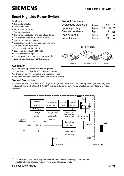
2
IN
Temperature sensor
5
Load
4
ST
Short circuit detection
GND
® PROFET
Load GND
1
Signal GND
1) 2)
No external components required, reverse load current limited by connected load. Additional external diode required for charged inductive loads
Semiconductor Group
1
04.96
元器件交易网
BTS 442 E2
Pin 1 2 3 4 5 Symbol GND IN Vbb ST OUT (Load, L) I + S O Function Logic ground Input, activates the power switch in case of logical high signal Positive power supply voltage, the tab is shorted to this pin Diagnostic feedback, low on failure Output to the load
Semiconductor Group
3
元器件交易网
BTS 442 E2
Parameter and Conditions
at Tj = 25 °C, Vbb = 12 V unless otherwise specified
Tj=25 °C: RON Tj=150 °C: IL(ISO) IL(GNDhigh)
1N4462中文资料
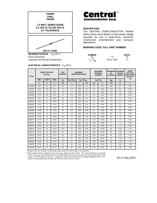
1N4460 THRU 1N4496 1.5 WATT ZENER DIODE 6.2 VOLTS TO 200 VOLTS 5% TOLERANCE
Central
TM
Semiconductor Corp.
DESCRIPTION: The CENTRAL SEMICONDUCTOR 1N4460 Series silicon zener diode is a high quality voltage regulator for use in automotive, industrial, commercial, entertainment and computer applications. MARKING CODE: FULL PART NUMBER
ZENER VOLTAGE VZ @ IZT TYPE MIN V 1N4481 1N4482 1N4483 1N4484 1N4485 1N4486 1N4487 1N4488 1N4489 1N4490 1N4491 1N4492 1N4493 1N4494 1N4495 1N4496 44.65 48.45 53.20 58.90 64.60 71.25 77.90 86.45 95.00 104.5 114.0 123.5 142.5 152.0 171.0 190.0 NOM V 47 51 56 62 68 75 82 91 100 110 120 130 150 160 180 200 MAX V 49.35 53.55 58.80 65.10 71.40 78.75 86.10 95.55 105.0 115.5 126.0 136.5 157.5 168.0 189.0 210.0
IZT mA 5.5 5.0 4.5 4.0 3.7 3.3 3.0 ቤተ መጻሕፍቲ ባይዱ.8 2.5 2.3 2.0 1.9 1.7 1.6 1.4 1.2
MAX5222中文资料完整

令中。
Figure 图 3.详细的串行接口时序图
数字输入 数字输入与 CMOS 逻辑兼容。当通过 0.3 ✕ VDD 和 0.7 ✕ VDD 之间的过渡区切换逻辑 输入时,电源电流稍微增加。 微处理器接口 MAX5222 串行接口与 Microwire、SPI 和 QSPI 兼容。对于 SPI,清除 CPOL 和 CPHA 位 (CPOL=0 和 CPHA=0)。cpol=0 将非活动时 钟状态设置为零,CPHA=0 更改 SCLK 下降沿 的数据。此设置允许 SPI 以全时钟速度运行。 如果您的祄 P 上没有串行端口,则可以使用 并行端口的 3 位逐位模拟串行端口操作。只 有在必要时才操作串行时钟,从而使电压输 出处的数字馈通最小化。
工作温度范围…………-40°C 至+85°C
接 地 的 所 有 其 他 插 脚 ( 注 1 ) -0.3V 至 结温…………………………………+150°C
(VDD+0.3V)
储存温度范围……………………-65°C 至
持续功耗(Ta=+70°C)
+150°C
8 针 SOT23(在+70°C 以上减额 8.7mW/° 铅温度(焊接 10s)……………………………
CIN
Note4
10
pF
动态性能
电压输出滑移速率 电压输出稳定时间 数字馈通 和串扰
电源电压范围 电源电流
关机电源电流
SR
CL = 100pF
1
To ± 1⁄2LSB, CL = 100pF
10
All 0s to all 1s
0.25
电源
VDD
2.7
5.5
ALL INPUTS=0 IDD
1777442中文资料
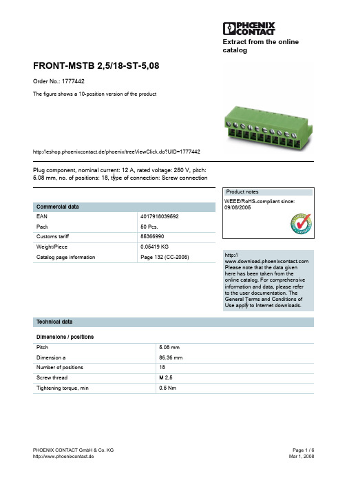
Extract from the onlinecatalogFRONT-MSTB 2,5/18-ST-5,08Order No.: 1777442The figure shows a 10-position version of the producthttp://eshop.phoenixcontact.de/phoenix/treeViewClick.do?UID=1777442Plug component, nominal current: 12 A, rated voltage: 250 V, pitch: 5.08 mm, no. of positions: 18, type of connection: Screw connectionhttp://Please note that the data givenhere has been taken from theonline catalog. For comprehensiveinformation and data, please referto the user documentation. TheGeneral Terms and Conditions ofUse apply to Internet downloads. Technical dataDimensions / positionsPitch 5.08 mmDimension a86.36 mmNumber of positions18Screw thread M 2,5Tightening torque, min0.5 NmTechnical dataInsulating material group IRated surge voltage (III/3) 4 kV Rated surge voltage (III/2) 4 kV Rated surge voltage (II/2) 4 kV Rated voltage (III/2)320 V Rated voltage (II/2)630 V Connection in acc. with standard EN-VDE Nominal current I N12 A Nominal voltage U N250 V Nominal cross section 2.5 mm2 Maximum load current12 A Insulating material PA Inflammability class acc. to UL 94V0 Internal cylindrical gage A3 Stripping length10 mmConnection dataConductor cross section solid min.0.34 mm2 Conductor cross section solid max. 2.5 mm2 Conductor cross section stranded min.0.2 mm2 Conductor cross section stranded max. 2.5 mm2 Conductor cross section stranded, with ferrule0.25 mm2 without plastic sleeve min.Conductor cross section stranded, with ferrule2.5 mm2 without plastic sleeve max.Conductor cross section stranded, with ferrule0.25 mm2 with plastic sleeve min.Conductor cross section stranded, with ferrule2.5 mm2 with plastic sleeve max.Conductor cross section AWG/kcmil min.24 Conductor cross section AWG/kcmil max122 conductors with same cross section, solid min.0.2 mm2 2 conductors with same cross section, solid max. 1 mm22 conductors with same cross section, stranded0.2 mm2 min.2 conductors with same cross section, strandedmax.1.5 mm22 conductors with same cross section, stranded,ferrules without plastic sleeve, min.0.25 mm22 conductors with same cross section, stranded,ferrules without plastic sleeve, max.1 mm22 conductors with same cross section, stranded,TWIN ferrules with plastic sleeve, min.0.5 mm22 conductors with same cross section, stranded,TWIN ferrules with plastic sleeve, max.1.5 mm2 Certificates / ApprovalsApproval logoCSANominal voltage U N300 VNominal current I N10 AAWG/kcmil22-12CULNominal voltage U N300 VNominal current I N10 AAWG/kcmil30-12ULNominal voltage U N300 VNominal current I N10 AAWG/kcmil30-12Certification CB, CSA, CUL, GOST, UL, VDE-PZIAccessoriesItem Designation DescriptionAssembly1763058FRONT-MSTB-EW Removal aid, for FRONT-MSTB, facilitates extraction of severalplugs mounted behind each otherBridges2303145EBL 2- 5Insertion bridge, 2-pos., fully insulated2303158EBL 3- 5Insertion bridge, 3-pos., fully insulated2303132EBL 10- 5Insertion bridge, 10-pos., divisible, fully insulatedGeneral2303161EBL 4- 5Insertion bridge, 4-pos., fully insulated2303174EBL 5- 5Insertion bridge, 5-pos., fully insulatedMarking1051993B-STIFT Marker pen, for manual labeling of unprinted Zack strips, smear-proof and waterproof, line thickness 0.5 mm0805108SK 5,08/2,8:SO Marker card, special printing, self-adhesive, labeled acc. tocustomer requirements, 14 identical marker strips per card, max.25-position labeling per strip, color: White0804293SK 5,08/3,8:FORTL.ZAHLEN Marker card, printed horizontally, self-adhesive, 12 identicaldecades marked 1-10, 11-20 etc. up to 91-(99)100, sufficient for120 terminal blocks0803883SK U/2,8 WH:UNBEDRUCKT Unprinted marker cards, DIN A4 format, pitch as desired, self-adhesive, with 50 stamped marker strips, 185 mm strip length, canbe labeled with the CMS system or manually with the M-PENPlug/Adapter1734634CP-MSTB Coding profile, is inserted into the slot on the plug or invertedheader, red insulating materialTools1205053SZS 0,6X3,5Screwdriver, bladed, matches all screw terminal blocks up to 4.0mm² connection cross section, blade: 0.6 x 3.5 mm, without VDEapprovalAdditional productsItem Designation DescriptionGeneral1824007ICC 2,5/18-STZ-5,08Plug component, nominal current: 12 A, rated voltage: 250 V,pitch: 5.08 mm, no. of positions: 18, type of connection: Crimpconnection1788884MSTBVK 2,5/18-G-5,08Header, nominal current: 12 A, rated voltage: 320 V, pitch: 5.08mm, no. of positions: 18, mounting: Mounting rail1788693MVSTBU 2,5/18-GB-5,08Header, nominal current: 12 A, rated voltage: 320 V, pitch: 5.08mm, no. of positions: 18, mounting: Direct mounting1769625SMSTB 2,5/18-G-5,08Header, nominal current: 12 A, rated voltage: 250 V, pitch: 5.08mm, no. of positions: 18, mounting: Soldering3002034UK 3-MSTB-5,08Modular terminal blocks with plug entry, cross section: 0.2 - 2.5mm², AWG: 30 - 12, width: 5.1 mm, color: gray3002076UK 3-MVSTB-5,08Modular terminal blocks with plug entry, cross section: 0.2 - 2.5mm², AWG: 26 - 12, width: 5.1 mm, color: gray3002102UK 3-MVSTB-5,08-LA 24RD Modular terminal block with plug entry, nominal current: 12 A,rated voltage: 320 V, pitch: 5.08 mm, no. of positions: 1, mounting:mounting rail, with red light indicator, voltage light indicator: 24 VAC/DC, current light indicator: 3.3 mA3002063UK 3-MVSTB-5,08/EK Modular terminal blocks with plug entry, cross section: 0.2-2.5mm², AWG: 26-12, width: 5.1 mm, color: blue3002131UK 3D-MSTBV-5,08Modular terminal blocks with vertical plug entry, cross section: 0.2- 2.5 mm, AWG: 30 - 12, width: 5.1 mm, color: gray3002144UK 3D-MSTBV-5,08-LA 24RD Modular terminal block with vertical plug entry, color: Gray, withred light indicator, voltage light indicator: 24 V AC/DC, current lightindicator: 3.3 mA3002173UK 3D-MSTBV-5,08/EK Modular terminal blocks with plug entry, cross section: 0.2 - 2.5mm², AWG: 30 - 12, width: 5.1 mm, color: blue2770888UKK 3-MSTB-5,08Modular terminal blocks with 2 horizontal plug entries, crosssection: 0.2 - 2.5 mm, AWG: 30 - 12, width: 5.1 mm, color: gray 1876615UKK 3-MSTB-5,08-PE Ground terminal block, with 2 horizontal plug entries, nominalcurrent: 12 A, rated voltage: 320 V, pitch: 5.08 mm, no. ofpositions: 1, mounting: mounting rail.2770846UKK 3-MSTBVH-5,08Modular terminal blocks with vertical and horizontal plug entry,cross section: 0.2 - 2.5 mm, AWG: 30 - 12, width: 5.1 mm, color:gray1788279UMSTBVK 2,5/18-G-5,08Header, nominal current: 12 A, rated voltage: 320 V, pitch: 5.08mm, no. of positions: 18, mounting: Mounting rail1873016ZFKK 1,5-MSTBV-5,08Modular terminal blocks with plug entry, cross section: 0.2 - 1.5mm², width: 5.1 mm, color: grayDrawingsDimensioned drawingAddressPHOENIX CONTACT GmbH & Co. KGFlachsmarktstr. 832825 Blomberg,GermanyPhone +49 5235 3 00Fax +49 5235 3 41200http://www.phoenixcontact.de© 2008 Phoenix ContactTechnical modifications reserved;。
MA44769中文资料

V3.00Step Recovery DiodesMA43000,MA44600,MA44700 SeriesFeaturesq Low Transition Times q Tight Capacitance RangesqHigh Voltage and Low Thermal Resistance for Higher Input PowerqSurface Mount Package Available (SOT-23)DescriptionThe MA44600 series of Step Recovery diodes is designed for use in low and moderate power multipliers with out-put frequencies of up to 20 GHz. These Step Recovery diodes generate harmonics by storing a charge as the diode is driven to forward conductance by the positive voltage of the input signal. When the signal reverses polarity, this charge is extracted. The Step Recovery diode will appear as a low impedance current source until all the charge is extracted, then it will “snap” to a higher imped-ance. This causes a voltage pulse to form in the impulse circuit of the multiplier. Step Recovery diodes make excellent high order multipliers such as comb generators.They are also useful as efficient moderate power X2- X4multipliers.ApplicationsHigh Order Narrow Band Moderate Power Multipliers (MA44600 series)Comb Generators (MA43592, MA43543)High Power Circuit Tested Multiplier (MA43000 Series)Surface Mount Low Power Multipliers (MA44700 Series)V3.00 Electrical Specifications @ 25°CSnap VaractorsNotes:1.When ordering, specify the desired case style by adding the case des-ignation as a suffix to the model number.Case styles for the MA44600series are 30, 91 and 93.To order in chip form, add the suffix “134”tothe model number.The nominal chip size for the MA44600 series is15 mils.2.Reverse voltage (V R) is measured at a reverse bias current of 10 µA.3.Junction capacitance is measured at a reverse voltage of 6 volts and afrequency of 1 MHz.4.Transition time is measured between 20% and 80% points on the volt-age recovery trace.Test conditions are +10 mA and -10 volts. Case Styles (See appendix for complete dimensions)309193134Notes:1.The standard case styles are indicated for each model number.Other case styles are available.Consult the factory for information.High Power Circuit Tested Step Recovery DiodesMin./Max.3Junction Min./Max.Maximum Maximum CapacitanceLifetime,T L Snap Time,T S Thermal Model C j 10 mA/6 mA-10V/10 mAResistance,jcNumber (pF)(ns)(ps)(C/W)MA43000 3 - 4.50250 - 50060012MA43002 1.60 - 2.4075 - 22525025MA430040.45 - 0.8520 - 5015045Surface Mount Step Recovery Diodes (SOT-23)2.Reverse voltage is measured at reverse bias current of 10 µA.3.Junction capacitance is measured at a reverse bias of 6 volts and a frequency of 1 MHz.Case styles (See appendix for complete dimensions)91103SOT -23 (High Profile)Notes:1.The standard case styles are indicated for each model number.For other available case styles, consult the factory.2.This is an operable output frequency range and does not imply instan-taneous bandwidth.Min./Max.4Maximum 2Min./Max.3Junction Min./Max.Maximum Maximum Nominal 2Input Reverse CapacitanceCarrier Snap Time,T S Thermal Output Model Case 1Power Voltage V R Cj Lifetime,T L-10V/10 mAResistance Frequency Number Style (Watts)(Volts)(pF)(ps)(ps)jc(C/W)(GHz)MA4359230 1.025 - 400.2 - 0.309 - 279070 1 - 12MA43543931.520 - 500.2 - 0.5510 - 25601252 - 20Absolute Maximum Ratings @ 25°CEnvironmental PerformanceThe MA44600 and MA43000 series of diodes in ceramic packages are capable of meeting the tests dictated by the methods and procedures of the latest revisions of MIL-S-19500, MIL-STD-202 and MIL-STD-750 which specify mechanical, electrical, thermal and other environmental tests common to military semiconductor products.High Order Step Recovery Diode Varactors for Use in Comb GenerationCase Styles (See appendix for complete dimensions)3.Breakdown voltage is measured at a reverse bias voltage of 10 µA.4.Junction capacitance is measured at a reverse bias voltage of 6 volts and a frequency of 1 MHz.3093。
BTS442E2_99中文资料

Symbol
Values min typ max
Unit
Load Switching Capabilities and Characteristics On-state resistance (pin 3 to 5)
IL = 5 A
Nominal load current (pin 3 to 5) ISO Proposal: VON = 0.5 V, TC = 85 °C Output current (pin 5) while GND disconnected or GND pulled up, VIN= 0, see diagram page 7, Tj =-40...+150°C Turn-on time to 90% VOUT: Turn-off time to 10% VOUT: RL = 12 Ω, Tj =-40...+150°C Slew rate on 10 to 30% VOUT, RL = 12 Ω, Tj =-40...+150°C Slew rate off 70 to 40% VOUT, RL = 12 Ω, Tj =-40...+150°C
see internal circuit diagrams page 6...
Symbol Vbb VLoad dump3)
Values 63 80 self-limited -40 ...+150 -55 ...+150 167 2.1 2.0 -0.5 ... +6 ±5.0 ±5.0 ≤ 0.75 ≤ 75 ≤ tbd
元器件交易网 PROFET® BTS 442 E2
Smart Highside Power Switch
Features
HS2MA中文资料
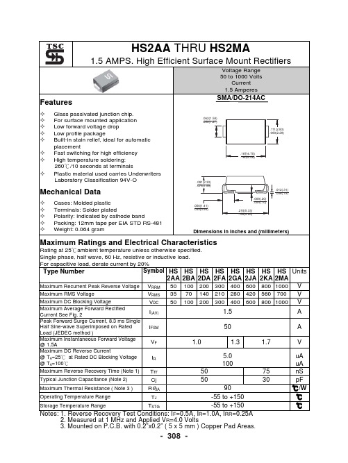
90 -55 to +150 Storage Temperature Range TSTG -55 to +150 Notes: 1. Reverse Recovery Test Conditions: I F=0.5A, IR=1.0A, IRR=0.25A 2. Measured at 1 MHz and Applied VR=4.0 Volts 3. Mounted on P.C.B. with 0.2”x0.2” ( 5 x 5 mm ) Copper Pad Areas.
100
Tj=100 0C
1
10
Tj=25 0C
0.1
0.1
0.001 0 20 40 60 80 100 120 1408
A-HS
2MA
1
0.01
HS2 AA-H S2D A
HS 2G A
1.0
1.2
1.4
PERCENT OF RATED PEAK REVERSE VOLTAGE. (%)
FIG.2- MAXIMUM FORWARD CURRENT DERATING CURVE
AVERAGE FORWARD CURRENT. (A)
3.0 2.5 2.0 1.5 1.0 0.5 0 0 25 50 75 100 125 150 175
o
SINGLE PHASE HALF WAVE 60Hz RESISTIVE OR INDUCTIVE LOAD 0.375" (9.5mm) LEAD LENGTH
NOTES: 1. Rise Time=7ns max. Input Impedance= 1 megohm 22pf 2. Rise Time=10ns max. Sourse Impedance= 50 ohms
MA44631B中文资料
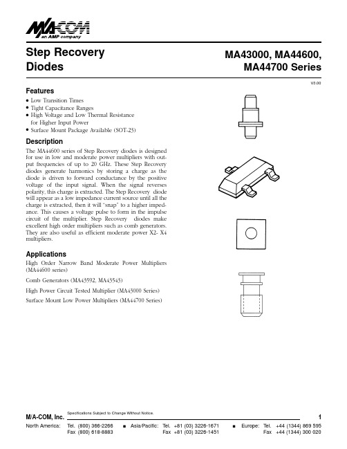
V3.00Step Recovery DiodesMA43000,MA44600,MA44700 SeriesFeaturesq Low Transition Times q Tight Capacitance RangesqHigh Voltage and Low Thermal Resistance for Higher Input PowerqSurface Mount Package Available (SOT-23)DescriptionThe MA44600 series of Step Recovery diodes is designed for use in low and moderate power multipliers with out-put frequencies of up to 20 GHz. These Step Recovery diodes generate harmonics by storing a charge as the diode is driven to forward conductance by the positive voltage of the input signal. When the signal reverses polarity, this charge is extracted. The Step Recovery diode will appear as a low impedance current source until all the charge is extracted, then it will “snap” to a higher imped-ance. This causes a voltage pulse to form in the impulse circuit of the multiplier. Step Recovery diodes make excellent high order multipliers such as comb generators.They are also useful as efficient moderate power X2- X4multipliers.ApplicationsHigh Order Narrow Band Moderate Power Multipliers (MA44600 series)Comb Generators (MA43592, MA43543)High Power Circuit Tested Multiplier (MA43000 Series)Surface Mount Low Power Multipliers (MA44700 Series)V3.00 Electrical Specifications @ 25°CSnap VaractorsNotes:1.When ordering, specify the desired case style by adding the case des-ignation as a suffix to the model number.Case styles for the MA44600series are 30, 91 and 93.To order in chip form, add the suffix “134”tothe model number.The nominal chip size for the MA44600 series is15 mils.2.Reverse voltage (V R) is measured at a reverse bias current of 10 µA.3.Junction capacitance is measured at a reverse voltage of 6 volts and afrequency of 1 MHz.4.Transition time is measured between 20% and 80% points on the volt-age recovery trace.Test conditions are +10 mA and -10 volts. Case Styles (See appendix for complete dimensions)309193134Notes:1.The standard case styles are indicated for each model number.Other case styles are available.Consult the factory for information.High Power Circuit Tested Step Recovery DiodesMin./Max.3Junction Min./Max.Maximum Maximum CapacitanceLifetime,T L Snap Time,T S Thermal Model C j 10 mA/6 mA-10V/10 mAResistance,jcNumber (pF)(ns)(ps)(C/W)MA43000 3 - 4.50250 - 50060012MA43002 1.60 - 2.4075 - 22525025MA430040.45 - 0.8520 - 5015045Surface Mount Step Recovery Diodes (SOT-23)2.Reverse voltage is measured at reverse bias current of 10 µA.3.Junction capacitance is measured at a reverse bias of 6 volts and a frequency of 1 MHz.Case styles (See appendix for complete dimensions)91103SOT -23 (High Profile)Notes:1.The standard case styles are indicated for each model number.For other available case styles, consult the factory.2.This is an operable output frequency range and does not imply instan-taneous bandwidth.Min./Max.4Maximum 2Min./Max.3Junction Min./Max.Maximum Maximum Nominal 2Input Reverse CapacitanceCarrier Snap Time,T S Thermal Output Model Case 1Power Voltage V R Cj Lifetime,T L-10V/10 mAResistance Frequency Number Style (Watts)(Volts)(pF)(ps)(ps)jc(C/W)(GHz)MA4359230 1.025 - 400.2 - 0.309 - 279070 1 - 12MA43543931.520 - 500.2 - 0.5510 - 25601252 - 20Absolute Maximum Ratings @ 25°CEnvironmental PerformanceThe MA44600 and MA43000 series of diodes in ceramic packages are capable of meeting the tests dictated by the methods and procedures of the latest revisions of MIL-S-19500, MIL-STD-202 and MIL-STD-750 which specify mechanical, electrical, thermal and other environmental tests common to military semiconductor products.High Order Step Recovery Diode Varactors for Use in Comb GenerationCase Styles (See appendix for complete dimensions)3.Breakdown voltage is measured at a reverse bias voltage of 10 µA.4.Junction capacitance is measured at a reverse bias voltage of 6 volts and a frequency of 1 MHz.3093。
MAX232中文资料(官方版)
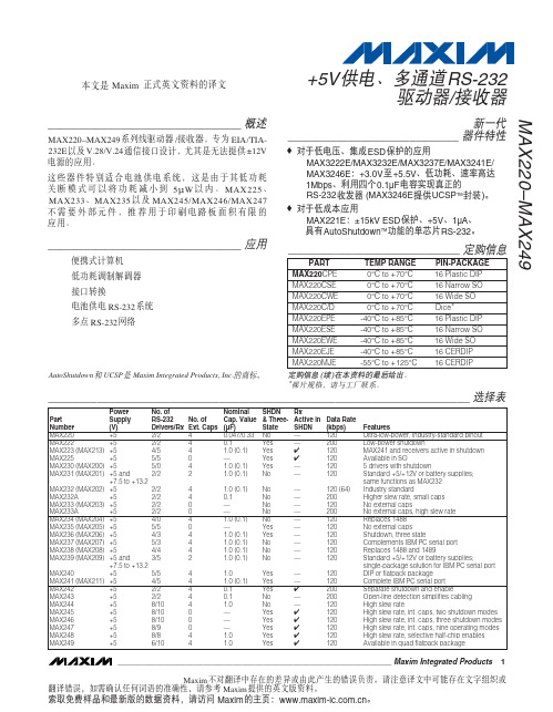
新一代 器件特性 ____________________________
♦ 对于低电压、集成 ESD 保护的应用 MAX3222E/MAX3232E/MAX3237E/MAX3241E/ MAX3246E:+3.0V 至 +5.5V、低功耗、速率高达 1Mbps、利用四个 0.1µF 电容实现真正的 RS-232 收发器 (MAX3246E 提供 UCSPTM 封装 )。 ♦ 对于低成本应用 MAX221E:±15kV ESD 保护、+5V、1µA、 具有 AutoShutdownTM 功能的单芯片 RS-232。
________________________________ 应用
便携式计算机 低功耗调制解调器 接口转换 电池供电 RS-232 系统 多点 RS-232 网络
_____________________________ 定购信息
PART MAX220CPE MAX220CSE MAX220CWE MAX220C/D MAX220EPE MAX220ESE MAX220EWE MAX220EJE MAX220MJE TEMP RANGE 0°C to +70°C 0°C to +70°C 0°C to +70°C 0°C to +70°C -40°C to +85°C -40°C to +85°C -40°C to +85°C -40°C to +85°C -55°C to +125°C PIN-PACKAGE 16 Plastic DIP 16 Narrow SO 16 Wide SO Dice* 16 Plastic DIP 16 Narrow SO 16 Wide SO 16 CERDIP 16 CERDIP
ZMM5252B中文资料(WILLAS ELECTRONIC)中文数据手册「EasyDatasheet - 矽搜」
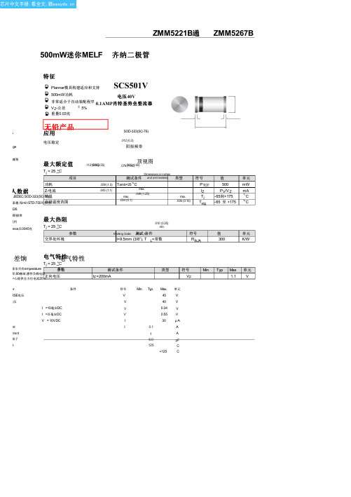
5264
ZMM5265B
62.0
58.90
65.10
185
2.0
1400
0.25
0.1
47.0
5265
ZMM5266B
68.0
64.60
71.40
230
1.8
1600
0.25
0.1
52.0
5266
ZMM5267B
75.0
71.25
78.75
270
1.7
1700
0.25
0.1
56.0
5267
1)基于直流测量达到热平衡;引线长度=9.5毫米(3/8");散热器= 30K / W热阻
5244
ZMM5245B
15.0
14.25
15.75
16
8.5
600
0.25
0.1
11.0
5245
ZMM5246B
16.0
15.20
16.80
17
7.8
600
0.25
0.1
12.0
5246
ZMM5247B
17.0
16.15
17.85
19
7.4
600
0.25
0.1
13.0
5247
ZMM5248B
18.0
类型
max. .006 (0.15)
符号
PTOT IZ Tj Tstg
值
500
PV/V Z -65到+175 –65 至 +175
单元
mW
mA °C °C
.010 (0.25) min.
Marking Code: 测JV o试r 4条件
6222中文资料

HCMOS OUTPUT CHARACTERISTICS
PARAMETER LOAD Voltage (High) (Low) Current (High) (Low) Duty Cycle at 50% of Vcc Rise / Fall Time 10% to 90% Start-Up Time Jitter (BW=10Hz to 20MHz) Jitter (BW=12kHz to 20MHz) MINIMUM 0.9Vcc -4 45 NOMINAL MAXIMUM 15 0.1Vcc 4 55 5 10 5 1 UNITS pF Vdc Vdc mA mA % nS h) (Vol) (Ioh) (Ioh)
50 -
PACKAGE CHARACTERISTICS
Package Hermetically sealed ceramic package and metal cover
TABLE 6.0
POWER SAVING FUNCTION: 10uA WHEN DISABLED CERAMIC SURFACE MOUNT PACKAGE TAPE AND REEL PACKAGING
TABLE 5.0 NOTE
FEATURES 2.5V OPERATION 1.8 to 50MHz TEMPERATURE RANGE: -40 to 85°C OVERALL FREQUENCY TOLERANCE:±50ppm TRI-STATE ENABLE/DISABLE FUNCTION
元器件交易网
THE CONNOR-WINFIELD CORP.
2111 COMPREHENSIVE DRIVE. AURORA, IL 60505. FAX (630) 851-5040. PHONE (630) 851-4722.
双相不锈钢(1.4462或4462不锈钢)

双相不锈钢(1.4462或4462不锈钢)什么是1.4462材质?双相不锈钢(1.4462或4462不锈钢)是一种极耐腐蚀的不锈钢牌号。
这些质量为4462的不锈钢比304和316质量的材料具有更高的防锈性,并且在化学上既是奥氏体不锈钢又是铁素体不锈钢。
它们比不锈钢更硬,对奥氏体材料的抵抗力是不锈钢的两倍。
在我国,这种不锈钢品质也被称为“双相不锈钢”(英文名称)。
1.4462 Mepa金属是船用材料和游艇轴中最常用的不锈钢材料之一,具有耐腐蚀性和机械强度。
1.4462材料属性规格:EN 10088-2:2005片材-厚达8毫米规格:EN 10088-2:2005板-超过8毫米至13.5毫米厚一、1.4462对应牌号:1、国标GB-T标准:数字牌号:S22253、新牌号:022Cr22Ni5Mo3N、旧牌号:00Cr22Ni5Mo3N,2、美标:ASTMA 标准:S31803,SAE标准:一,UNS标准:F51,3、日标JIS标准:329J3L,dp8,4、德标DIN标准:1.4462,5、欧标EN标准:X2CrNiMo22-5-3,X2CrNiMoN22-5-3。
二、1.4462化学成分:⑴碳C:≤0.030,⑵硅Si:≤1.00,⑶锰Mn:≤2.00,⑷磷P:≤0.030,⑸硫S:≤0.020,⑹铬Cr:21.00~23.00,⑺镍Ni:4.50~6.50,⑻钼Mo:2.50~3.50,⑼氮N:0.08~0.20,⑽铜Cu:—,⑾其它元素:—。
三、1.4462物理性能:①密度密度(20℃)/kg/dm3:7.8,②熔点/℃:1420~1462,③比热(0~100℃)/kg/(kg.k):0.5,④热导率/w/(m.k)100℃-:19,⑸热导率/w/(m.k)500℃-:23,⑥线胀系数/(10-6/k)0~100℃:13.7,⑦线胀系数/(10-6/k)0~561℃:14.7,⑧电阻率(20℃)/(Ω.mm2/m):0.88,⑨向弹性模量(20℃)/GPa:186,⑩磁性:有。
2P4M中文资料(nec)中文数据手册「EasyDatasheet - 矽搜」

DRM,
Tj = 125°C
−
Tj = 25°C
−
Tj = 125°C
−
dV D/dt Tj = 125°C, V DM = 2/3 V DRM
10
−
VTM ITM = 4 A
−
IGT VDM = 6 V, R L = 100 Ω,
−
栅极触发电压
Note
VGT VDM = 6 V, R L = 100 Ω,
1985, 2006
The revised points can be easily searched by copying an "现场:修订部分可以通过在 PDF文件中复制一个 “R”,并在 “查找内容 ”指定它可以很容易地搜索 .
芯片中文手册,看全文,戳
2P4M,2P6M
最大额定值
Note
IH VDM = 24 V, I TM = 4 A
−
1
3
mA 参照图9
电路改判关断时间
tq
Tj = 125°C, I TM = 500毫安,
−
30
−
μs
−
diR / DT = 15 A /μs, V R ≥ 25 V,
VDM = 2/3 V DRM ,DV D / dt的= 10V μ/ s
特性
符号
非重复性峰值反向电压 非重复性峰值断态电压 重复峰值反向电压 重复峰值断态电压
Note Note Note Note
VRSM VDSM VRRM VDRM
通态电流
IT (AV)
有效的通态电流 浪涌不重复通态电流 熔断电流
IT (RMS)
IT S M
∫
i2
MA46422中文资料
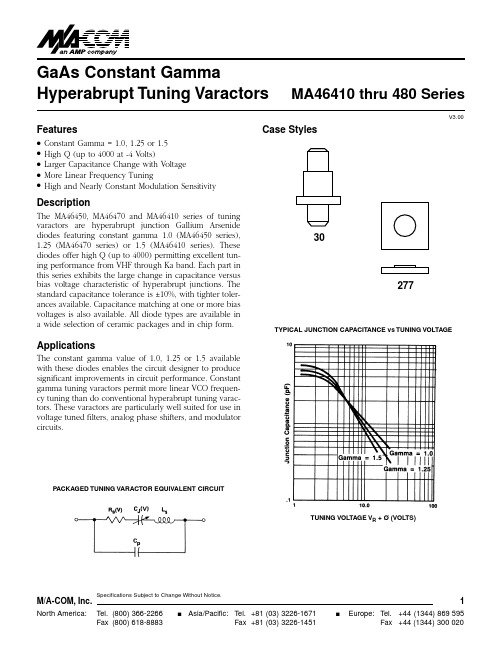
V3.00GaAs Constant GammaHyperabrupt Tuning VaractorsMA46410 thru 480 SeriesFeaturesq Constant Gamma = 1.0, 1.25 or 1.5q High Q (up to 4000 at -4 Volts)q Larger Capacitance Change with Voltage q More Linear Frequency TuningqHigh and Nearly Constant Modulation SensitivityDescriptionThe MA46450, MA46470 and MA46410 series of tuning varactors are hyperabrupt junction Gallium Arsenide diodes featuring constant gamma 1.0 (MA46450 series),1.25 (MA46470 series) or 1.5 (MA46410 series). These diodes offer high Q (up to 4000) permitting excellent tun-ing performance from VHF through Ka band. Each part in this series exhibits the large change in capacitance versus bias voltage characteristic of hyperabrupt junctions. The standard capacitance tolerance is ±10%, with tighter toler-ances available. Capacitance matching at one or more bias voltages is also available. All diode types are available in a wide selection of ceramic packages and in chip form.ApplicationsThe constant gamma value of 1.0, 1.25 or 1.5 available with these diodes enables the circuit designer to produce significant improvements in circuit performance. Constant gamma tuning varactors permit more linear VCO frequen-cy tuning than do conventional hyperabrupt tuning varac-tors. These varactors are particularly well suited for use in voltage tuned filters, analog phase shifters, and modulatorcircuits.Case Styles30277V3.00* The maximum storage and operating temperature of the plastic1088 case style is 125°C.Absolute Maximum Ratings at +25°CElectrical Specifications at 25°CMA46450 SeriesGamma = 1.0Reverse Voltage 6= 22 Volts minimum Gamma 4= 0.9 - 1.1, V R = 2 - 20 VoltsJunction Capacitance Ratio (C J2/C J20) = 5.0 - 8.0MA46470 SeriesGamma = 1.25Reverse Voltage 6= 22 Volts minimum Gamma 4= 1.13 - 1.38, V R = 2 - 20 VoltsJunction Capacitance Ratio (C J2/C J20) = 8.15 - 12.99Notes:1.All GaAs tuning varactors are available in chip form as well as the case styles shown on the following page.When ordering, specify the desired case by adding the case designation as a suffix to the type number.2.Case parasitics (C p and L s ) are given for most case styles along with case outlines in the appendix.The Cp values listed typically have toler-ances of ±0.02 pF .3.The nominal tolerance at -4 Volts is ±10%.Closer tolerances are avail-able upon request.By adding the suffix A to the part number, a toler-ance of ±5% at -4 Volts is guaranteed.4.The values guaranteed for gamma are measured on unpackaged chips.The total capacitance versus bias voltage curve will deviateslightly from the chip capacitance versus bias voltage curve due to the package parasitic capacitance (Cp).5.Capacitance is measured at 1 MHz.6.Reverse voltage (V B ) is measured at 10 microamps.7.The total capacitance and capacitance ratios shown are for diodes housed in case style 30.Other case styles will result in different val-ues.Total 2, 6, 7Total50 MHz Capacitance Capacitance 7Q at Model Case 1@ -4 Volts Ratio (2/12)-4 Volts Number Style Min./Max.(pF)Min./Max.Typical MA46410300.45-0.60 2.7-4.33000MA46413300.90-1.10 4.2-5.72500MA4641630 1.62-1.98 5.2-4.92500MA4641830 2.42-2.97 5.7-7.61800MA4642030 3.33-4.22 6.0-8.11800MA4642130 4.22-5.17 6.2-8.31200MA4642230 5.04-6.16 6.3-8.41200MA46425309.00-11.006.6-8.81200Environmental Ratings PER MIL-STD-750MIL MethodLevelStorage Temperature 1031See maximum ratingsTemperature Cycle 105110 cycles, -65°C to +175°C Shock 2016500 g’s Vibration 205615 g’s Constant Acceleration 200620,000 g’s Humidity 102110 daysMA46410 Series Gamma = 1.5Breakdown Voltage 6= 18 Volts minimum Gamma 4= 1.4 - 1.6, V R = 2 - 12 VoltsJunction Capacitance Ratio (C J2/C J12) = 6.2 - 10.84V3.00 Case Styles (See appendix for complete dimensions).1100V R(VOLTS).1100V R(VOLTS).1100V R(VOLTS).1100V R(VOLTS).1110100V R(VOLTS)V R(VOLTS).1110100V R(VOLTS)。
MP4462
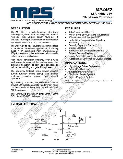
MP44623.5A, 4MHz, 36V Step-Down ConverterMPS CONFIDENTIAL AND PROPRIETARY INFORMATION – INTERNAL USE ONLYThe Future of Analog IC Technology DESCRIPTIONThe MP4462 is a high frequency step-downFEATURES• 100µA Quiescent Current=MPS CONFIDENTIAL AND PROPRIETARY INFORMATION – INTERNAL USE ONLYELECTRICAL CHARACTERISTICS (continued)V = 12V, V = 2.5V, V = 1.4V, T= +25°C, unless otherwise noted.TYPICAL PERFORMANCE CHARACTERISTICSV IN = 12V, C1 = 10µF, C2 = 22µF, L = 10µH and T A = +25°C, unless otherwise noted.Oscillating FrequencyTYPICAL PERFORMANCE CHARACTERISTICS (continued)V IN = 12V, C1 = 10µF, C2 = 22µF, L = 10µH and T A = +25°C, unless otherwise noted.1ms/div.Startup 1ms/div.Shutdown 1ms/div.Startup1ms/div.BLOCK DIAGRAMError AmplifierThe error amplifier compares the FB pin voltage with the internal reference (REF) and outputs a current proportional to the difference between the two. This output current is then used to Internal Soft-StartThe soft-start is implemented to prevent the converter output voltage from overshooting during startup. When the chip starts, the internal circuitry generates a soft-start voltageAt higher duty cycle operation condition, the time period available to the bootstrap charging is less so the bootstrap capacitor may not be sufficiently charged.In case the internal circuit does not haveStartup and ShutdownIf both VIN and EN are higher than their appropriate thresholds, the chip starts. The reference block starts first, generating stable reference voltage and currents, and then theAPPLICATION INFORMATIONCOMPONENT SELECTIONSetting the Output VoltageThe output voltage is set using a resistiveA good rule for determining the inductance to use is to allow the peak-to-peak ripple current in the inductor to be approximately 30% of theTable 1—Inductor Selection GuideThe input capacitor (C1) can be electrolytic, tantalum or ceramic. When using electrolytic or tantalum capacitors, a small, high quality ceramic capacitor, i.e. 0.1µF, should be placed as close to the IC as possible. When usingMP4462 can be optimized for a wide range of capacitance and ESR values.Compensation ComponentsMP4462 employs current mode control for easy compensation and fast transient response. The system stability and transient response are controlled through the COMP pin. COMP pin isIn this case (as shown in Figure 2), a third pole set by the compensation capacitor (C6) and the compensation resistor (R3) is used to compensate the effect of the ESR zero on the loop gain. This pole is located at:1. Choose the compensation resistor (R3) to set the desired crossover frequency. Determine the R3 value by the following equation:OUTC V f 2C 23R ×××π=High Frequency OperationThe switching frequency of MP4462 can be programmed up to 4MHz by an external resistor. Please pay attention to the following if the switching frequency is above 2MHz. Layout becomes more important when the device switches at higher frequency. It is essential to place the input decoupling capacitor, catch diode and the MP4462 (Vin pin, SW pin and PGND) as close as possible, withExternal Bootstrap DiodeIt is recommended that an external bootstrap diode be added when the input voltage is no greater than 5V or the 5V rail is available in the system. This helps improve the efficiency of the This diode is also recommended for high duty cycle operation (when V OUT /V IN>65%) or low V IN (<5Vin) applications.At no load or light load, the converter may operate in pulse skipping mode in order toTYPICAL APPLICATION CIRCUITSC4PACKAGE INFORMATION3mm x 3mm QFN10SOIC8E (EXPOSED PAD)NOTICE: The information in this document is subject to change without notice. Users should warrant and guarantee that third party Intellectual Property rights are not infringed upon when integrating MPS products into any application. MPS will not assume any legal responsibility for any said applications.。
ams 4462标准
ams 4462标准
AMS 4462标准是一种用于描述和分类金属材料的标准,它是由美国材料与试验协会(ASTM)制定的。
该标准主要用于航空航天领域,因为它涵盖了一些在航空航天领域常用的特殊合金材料,例如不锈钢和高强度铝合金等。
在AMS 4462标准中,每种金属材料都有一个特定的分类,这些分类基于材料的化学成分、机械性能、耐腐蚀性、加工性能等方面的特性。
这些分类有助于确保材料在使用过程中具有所需的性能和可靠性,并且符合航空航天领域的严格要求。
如果您需要了解有关AMS 4462标准的更多信息,建议查阅ASTM官方网站或相关技术文献。
- 1、下载文档前请自行甄别文档内容的完整性,平台不提供额外的编辑、内容补充、找答案等附加服务。
- 2、"仅部分预览"的文档,不可在线预览部分如存在完整性等问题,可反馈申请退款(可完整预览的文档不适用该条件!)。
- 3、如文档侵犯您的权益,请联系客服反馈,我们会尽快为您处理(人工客服工作时间:9:00-18:30)。
V3.00
Step Recovery Diodes
MA43000,MA44600,
MA44700 Series
Features
q Low Transition Times q Tight Capacitance Ranges
q
High Voltage and Low Thermal Resistance for Higher Input Power
q
Surface Mount Package Available (SOT-23)
Description
The MA44600 series of Step Recovery diodes is designed for use in low and moderate power multipliers with out-put frequencies of up to 20 GHz. These Step Recovery diodes generate harmonics by storing a charge as the diode is driven to forward conductance by the positive voltage of the input signal. When the signal reverses polarity, this charge is extracted. The Step Recovery diode will appear as a low impedance current source until all the charge is extracted, then it will “snap” to a higher imped-ance. This causes a voltage pulse to form in the impulse circuit of the multiplier. Step Recovery diodes make excellent high order multipliers such as comb generators.They are also useful as efficient moderate power X2- X4multipliers.
Applications
High Order Narrow Band Moderate Power Multipliers (MA44600 series)
Comb Generators (MA43592, MA43543)
High Power Circuit Tested Multiplier (MA43000 Series)
Surface Mount Low Power Multipliers (MA44700 Series)
V3.00 Electrical Specifications @ 25°C
Snap Varactors
Notes:
1.When ordering, specify the desired case style by adding the case des-
ignation as a suffix to the model number.Case styles for the MA44600
series are 30, 91 and 93.To order in chip form, add the suffix “134”to
the model number.The nominal chip size for the MA44600 series is
15 mils.
2.Reverse voltage (V R) is measured at a reverse bias current of 10 µA.
3.Junction capacitance is measured at a reverse voltage of 6 volts and a
frequency of 1 MHz.
4.Transition time is measured between 20% and 80% points on the volt-
age recovery trace.Test conditions are +10 mA and -10 volts. Case Styles (See appendix for complete dimensions)
309193134
Notes:
1.The standard case styles are indicated for each model number.Other case styles are available.Consult the factory for information.
High Power Circuit Tested Step Recovery Diodes
Min./Max.3Junction Min./Max.Maximum Maximum Capacitance
Lifetime,T L Snap Time,T S Thermal Model C j 10 mA/6 mA
-10V/10 mA
Resistance,jc
Number (pF)(ns)(ps)
(C/W)
MA43000 3 - 4.50250 - 50060012MA43002 1.60 - 2.4075 - 22525025MA43004
0.45 - 0.85
20 - 50
150
45
Surface Mount Step Recovery Diodes (SOT-23)
2.Reverse voltage is measured at reverse bias current of 10 µA.
3.Junction capacitance is measured at a reverse bias of 6 volts and a frequency of 1 MHz.
Case styles (See appendix for complete dimensions)
91103SOT -23 (High Profile)
Notes:
1.The standard case styles are indicated for each model number.For other available case styles, consult the factory.
2.This is an operable output frequency range and does not imply instan-taneous bandwidth.
Min./Max.4Maximum 2Min./Max.3Junction Min./Max.Maximum Maximum Nominal 2Input Reverse Capacitance
Carrier Snap Time,
T S Thermal Output Model Case 1Power Voltage V R Cj Lifetime,T L
-10V/10 mA
Resistance Frequency Number Style (Watts)
(Volts)(pF)
(ps)(ps)
jc(C/W)
(GHz)MA4359230 1.025 - 400.2 - 0.309 - 279070 1 - 12MA43543
93
1.5
20 - 50
0.2 - 0.55
10 - 25
60
125
2 - 20
Absolute Maximum Ratings @ 25°C
Environmental Performance
The MA44600 and MA43000 series of diodes in ceramic packages are capable of meeting the tests dictated by the methods and procedures of the latest revisions of MIL-S-19500, MIL-STD-202 and MIL-STD-750 which specify mechanical, electrical, thermal and other environmental tests common to military semiconductor products.
High Order Step Recovery Diode Varactors for Use in Comb Generation
Case Styles (See appendix for complete dimensions)
3.Breakdown voltage is measured at a reverse bias voltage of 10 µA.
4.Junction capacitance is measured at a reverse bias voltage of 6 volts and a frequency of 1 MHz.
3093。
