SR-B2A7B-FREQ中文资料
RX-2B

± 0.99 0.3
± 0.46 0.08
1.27MAX
杭州士兰微电子股份有限公司
10
版本号:1.1 2004.04.20
士兰半导体
附:
修改记录:
日期
2002.03.11 2002.03.21
版本号
1.0 1.1
描
原版 修改了“2. 编码/解码定时”
TX-2B/RX-2B
述
页码
6
杭州士兰微电子股份有限公司
左转 右转
后退 前进 加速
前进
加速
后退
16 15 14 13 12 11 10 9
RX-2B
12345678
右转 fosc=128kHz
左转
杭州士兰微电子股份有限公司
6
版本号:1.1 2004.04.20
士兰半导体
典型应用图例
发射部分
TX-2B/RX-2B
Ω Rosc=500k
14 13 12 11 10 9 8
3
14
Ω
Q5 473P Q6
Ω 1k
4
5
右转 6
左转 7
RX-2B
13
加速
12
11
后退
10
Ω,随 R1,R2,R3,R4=80~150 和 变化. VDD1 VDD2
8
9
R3
Ω 1k
Q7
Q8
Ω R4 1k
C945
M
C945
Q9 473P Q10
杭州士兰微电子股份有限公司
8
版本号:1.1 2004.04.20
士兰半导体
TX-2B/RX-2B
红外应用图例
发射部分
TMD0507-2A中文资料
SYMBOL VDD VGG Pin Tf Tstg
UNIT V V
dBm °CBiblioteka °CRATING 15 -10 20
-30 ∼ +80 -65 ∼ +175
RF PERFORMANCE SPECIFICATIONS ( Ta= 25°C )
CHARACTERISTICS Output Power at 1dB Compression Point Power Gain at 1dB Compression Point Gain Flatness (1)* Gain Flatness (2)** Drain Current*** Input VSWR
0.1 ±0.05
9
7-R0.4
2.0MIN.
11 ± 0.3
2.0MIN.
: VDD1 : RF IN : VDD2 : VGG : VDD3
: RF OUT : No Connection : VDD3 : GND
HANDLING PRECAUTIONS FOR PACKAGE MODEL Soldering iron should be grounded and the operating time should not exceed 10 seconds at
Rev. Mar. 2006
元器件交易网
TMD0507-2A
PACKAGE OUTLINE (2-11E1A)
C2.0
2.5 ± 0.3
Unit in mm
8-0.4±0.1
6-2.54 ±0.2 10 ±0.3 15 ±0.3 18 ±0.3
0.5 ±0.2 0.5 ±0.2 1.0 ±0.3 2.5MAX.
2MBI75S-120中文资料
Err
0
1
10
100
500
Gate resistance : Rg [ohm]
Collector current : Ic [ A ]
Switching loss : Eon, Eoff, Err [ mJ/pulse ]
ton tr
tf 100
50
0
20
40
60
80
100
120
Collector current : Ic [ A ]
Switching loss vs. Collector current (typ.) Vcc=600V, VGE=±15V, Rg=16ohm
20
Eon(125°C)
15
Eon(25°C)
10 Eoff(125°C)
Eoff(25°C)
5
Err(125°C)
Err(25°C)
0
0
20
40
60
80 100 120 140
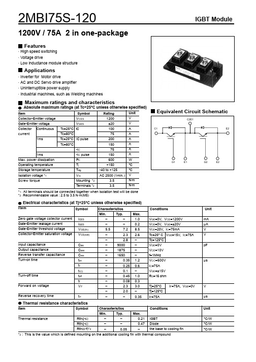
IGBT Module
180 160 140 120 100
80 60 40 20
0 0
Collector current vs. Collector-Emiiter voltage Tj= 125°C (typ.) VGE= 20V15V 12V
10V
8V
1
2
3
4
5
Collector - Emitter voltage : VCE [ V ]
Equivalent Circuit Schematic
C2E1
C1
E2
G1
E1
G2
E2
Electrical characteristics (at Tj=25°C unless otherwise specified)
英飞凌 FP50R12N2T7P EconoPIM 2 模块 数据表
EconoPIM ™2 模块 采用第七代沟槽栅/场终止IGBT7和第七代发射极控制二极管 带有温度检测NTC 和预涂导热介质特性•电气特性-V CES = 1200 V-I C nom = 50 A / I CRM = 100 A -沟槽栅IGBT7-低 V CEsat-过载操作达175°C•机械特性-高功率循环和温度循环能力-集成NTC 温度传感器-铜基板-低热阻的三氧化二铝 Al 2O 3 衬底-预涂导热介质-焊接技术可选应用•辅助逆变器•电机传动•伺服驱动器产品认证•根据 IEC 60747、60749 和 60068标准的相关测试,符合工业应用的要求。
描述FP50R12N2T7PEconoPIM ™2 模块内容描述 . . . . . . . . . . . . . . . . . . . . . . . . . . . . . . . . . . . . . . . . . . . . . . . . . . . . . . . . . . . . . . . . . . . . . . . . . . . . . . . . . . . . . . . . .1特性 . . . . . . . . . . . . . . . . . . . . . . . . . . . . . . . . . . . . . . . . . . . . . . . . . . . . . . . . . . . . . . . . . . . . . . . . . . . . . . . . . . . . . . . . .1可选应用 . . . . . . . . . . . . . . . . . . . . . . . . . . . . . . . . . . . . . . . . . . . . . . . . . . . . . . . . . . . . . . . . . . . . . . . . . . . . . . . . . . . .1产品认证 . . . . . . . . . . . . . . . . . . . . . . . . . . . . . . . . . . . . . . . . . . . . . . . . . . . . . . . . . . . . . . . . . . . . . . . . . . . . . . . . . . . .1内容 . . . . . . . . . . . . . . . . . . . . . . . . . . . . . . . . . . . . . . . . . . . . . . . . . . . . . . . . . . . . . . . . . . . . . . . . . . . . . . . . . . . . . . . . .2 1封装 . . . . . . . . . . . . . . . . . . . . . . . . . . . . . . . . . . . . . . . . . . . . . . . . . . . . . . . . . . . . . . . . . . . . . . . . . . . . . . . . . . . . . . . . .3 2IGBT, 逆变器 . . . . . . . . . . . . . . . . . . . . . . . . . . . . . . . . . . . . . . . . . . . . . . . . . . . . . . . . . . . . . . . . . . . . . . . . . . . . . . . . .3 3二极管,逆变器 . . . . . . . . . . . . . . . . . . . . . . . . . . . . . . . . . . . . . . . . . . . . . . . . . . . . . . . . . . . . . . . . . . . . . . . . . . . . . . .5 4二极管,整流器 . . . . . . . . . . . . . . . . . . . . . . . . . . . . . . . . . . . . . . . . . . . . . . . . . . . . . . . . . . . . . . . . . . . . . . . . . . . . . . .6 5IGBT, 斩波器 . . . . . . . . . . . . . . . . . . . . . . . . . . . . . . . . . . . . . . . . . . . . . . . . . . . . . . . . . . . . . . . . . . . . . . . . . . . . . . . . .7 6Diode-斩波器 . . . . . . . . . . . . . . . . . . . . . . . . . . . . . . . . . . . . . . . . . . . . . . . . . . . . . . . . . . . . . . . . . . . . . . . . . . . . . . . .8 7负温度系数热敏电阻 . . . . . . . . . . . . . . . . . . . . . . . . . . . . . . . . . . . . . . . . . . . . . . . . . . . . . . . . . . . . . . . . . . . . . . . . .9 8特征参数图表 . . . . . . . . . . . . . . . . . . . . . . . . . . . . . . . . . . . . . . . . . . . . . . . . . . . . . . . . . . . . . . . . . . . . . . . . . . . . . . .10 9电路拓扑图 . . . . . . . . . . . . . . . . . . . . . . . . . . . . . . . . . . . . . . . . . . . . . . . . . . . . . . . . . . . . . . . . . . . . . . . . . . . . . . . . .16 10封装尺寸 . . . . . . . . . . . . . . . . . . . . . . . . . . . . . . . . . . . . . . . . . . . . . . . . . . . . . . . . . . . . . . . . . . . . . . . . . . . . . . . . . . .16 11模块标签代码 . . . . . . . . . . . . . . . . . . . . . . . . . . . . . . . . . . . . . . . . . . . . . . . . . . . . . . . . . . . . . . . . . . . . . . . . . . . . . . .17修订历史 . . . . . . . . . . . . . . . . . . . . . . . . . . . . . . . . . . . . . . . . . . . . . . . . . . . . . . . . . . . . . . . . . . . . . . . . . . . . . . . . . . .18免责声明 . . . . . . . . . . . . . . . . . . . . . . . . . . . . . . . . . . . . . . . . . . . . . . . . . . . . . . . . . . . . . . . . . . . . . . . . . . . . . . . . . . .191封装表 1绝缘参数特征参数代号标注或测试条件数值单位绝缘测试电压V ISOL RMS, f = 50 Hz, t = 1 min 2.5kV 模块基板材料Cu内部绝缘基本绝缘 (class 1, IEC 61140)Al2O3爬电距离d Creep端子至散热器10.0mm 电气间隙d Clear端子至散热器7.5mm 相对电痕指数CTI>200相对温度指数 (电)RTI封装140°C 表 2特征值特征参数代号标注或测试条件数值单位最小值典型值最大值杂散电感,模块L sCE35nH 模块引线电阻,端子-芯片R AA'+CC'T H=25°C, 每个开关 5.5mΩ模块引线电阻,端子-芯片R CC'+EE'T H=25°C, 每个开关 4.8mΩ储存温度T stg-40125°C 最高基板工作温度T BPmax150°CM5, 螺丝36Nm 模块安装的安装扭距M根据相应的应用手册进行安装重量G180g注:The current under continuous operation is limited to 50 A rms per connector pin.Storage and shipment of modules with TIM => see AN2012-072IGBT, 逆变器表 3最大标定值特征参数代号标注或测试条件数值单位集电极-发射极电压V CES T vj = 25 °C1200V 连续集电极直流电流I CDC T vj max = 175 °C T H = 90 °C50A 集电极重复峰值电流I CRM t P = 1 ms100A 栅极-发射极峰值电压V GES±20V表 4特征值特征参数代号标注或测试条件数值单位最小值典型值最大值集电极-发射极饱和电压V CE sat I C = 50 A, V GE = 15 V T vj = 25 °C 1.50 1.80VT vj = 125 °C 1.64T vj = 175 °C 1.72栅极阈值电压V GEth I C = 2 mA, V CE = V GE, T vj = 25 °C 5.15 5.80 6.45V 栅极电荷Q G V GE = ±15 V, V CE = 600 V0.92µC 内部栅极电阻R Gint T vj = 25 °C0Ω输入电容C ies f = 100 kHz, T vj = 25 °C, V CE = 25 V, V GE = 0 V11.1nF 反向传输电容C res f = 100 kHz, T vj = 25 °C, V CE = 25 V, V GE = 0 V0.039nF 集电极-发射极截止电流I CES V CE = 1200 V, V GE = 0 V T vj = 25 °C0.01mA 栅极-发射极漏电流I GES V CE = 0 V, V GE = 20 V, T vj = 25 °C100nA开通延迟时间(感性负载)t don I C = 50 A, V CE = 600 V,V GE = ±15 V, R Gon = 7.5 ΩT vj = 25 °C0.059µs T vj = 125 °C0.061T vj = 175 °C0.062上升时间(感性负载)t r I C = 50 A, V CE = 600 V,V GE = ±15 V, R Gon = 7.5 ΩT vj = 25 °C0.043µs T vj = 125 °C0.047T vj = 175 °C0.049关断延迟时间(感性负载)t doff I C = 50 A, V CE = 600 V,V GE = ±15 V, R Goff = 7.5 ΩT vj = 25 °C0.290µs T vj = 125 °C0.380T vj = 175 °C0.420下降时间(感性负载)t f I C = 50 A, V CE = 600 V,V GE = ±15 V, R Goff = 7.5 ΩT vj = 25 °C0.110µs T vj = 125 °C0.200T vj = 175 °C0.270开通损耗能量 (每脉冲)E on I C = 50 A, V CE = 600 V,Lσ = 35 nH, V GE = ±15 V,R Gon = 7.5 Ω, di/dt = 900A/µs (T vj = 175 °C)T vj = 25 °C 5.07mJ T vj = 125 °C 6.76T vj = 175 °C7.72关断损耗能量 (每脉冲)E off I C = 50 A, V CE = 600 V,Lσ = 35 nH, V GE = ±15 V,R Goff = 7.5 Ω, dv/dt =2900 V/µs (T vj = 175 °C)T vj = 25 °C 3.37mJ T vj = 125 °C 5.31T vj = 175 °C 6.58(待续)表 4(续) 特征值特征参数代号标注或测试条件数值单位最小值典型值最大值短路数据I SC V GE≤ 15 V, V CC = 800 V,V CEmax=V CES-L sCE*di/dt t P≤ 8 µs,T vj=150 °C190At P≤ 7 µs,T vj=175 °C180结-散热器热阻R thJH每个 IGBT, Valid with IFX pre-appliedThermal Interface Material0.777K/W 允许开关的温度范围T vj op-40175°C注:T vj op > 150°C is allowed for operation at overload conditions. For detailed specifications, please refer to AN 2018-14.3二极管,逆变器表 5最大标定值特征参数代号标注或测试条件数值单位反向重复峰值电压V RRM T vj = 25 °C1200V 连续正向直流电流I F50A 正向重复峰值电流I FRM t P = 1 ms100A I2t-值I2t V R = 0 V, t P = 10 ms T vj = 125 °C465A²sT vj = 175 °C420表 6特征值特征参数代号标注或测试条件数值单位最小值典型值最大值正向电压V F I F = 50 A, V GE = 0 V T vj = 25 °C 1.72 2.10VT vj = 125 °C 1.59T vj = 175 °C 1.52反向恢复峰值电流I RM I F = 35 A, V R = 600 V,V GE = -15 V, -di F/dt = 900A/µs (T vj = 175 °C)T vj = 25 °C31A T vj = 125 °C39T vj = 175 °C45恢复电荷Q r I F = 50 A, V R = 600 V,V GE = -15 V, -di F/dt = 900A/µs (T vj = 175 °C)T vj = 25 °C 3.96µC T vj = 125 °C7.37T vj = 175 °C9.89(待续)表 6(续) 特征值特征参数代号标注或测试条件数值单位最小值典型值最大值反向恢复损耗(每脉冲)E rec I F = 50 A, V R = 600 V,V GE = -15 V, -di F/dt = 900A/µs (T vj = 175 °C)T vj = 25 °C 1.31mJ T vj = 125 °C 2.52T vj = 175 °C 3.46结-散热器热阻R thJH每个二极管, Valid with IFX pre-appliedThermal Interface Material1.13K/W 允许开关的温度范围T vj op-40175°C注:T vj op > 150°C is allowed for operation at overload conditions. For detailed specifications, please refer to AN 2018-14.4二极管,整流器表 7最大标定值特征参数代号标注或测试条件数值单位反向重复峰值电压V RRM T vj = 25 °C1600V 最大正向均方根电流(每芯片)I FRMSM T H = 60 °C70A最大整流器输出均方根电流I RMSM T H = 60 °C100A 正向浪涌电流I FSM t P = 10 ms T vj = 25 °C560AT vj = 150 °C435I2t-值I2t t P = 10 ms T vj = 25 °C1570A²sT vj = 150 °C945表 8特征值特征参数代号标注或测试条件数值单位最小值典型值最大值正向电压V F I F = 50 A T vj = 150 °C 1.05V 反向电流I r T vj = 150 °C, V R = 1600 V1mA 结-散热器热阻R thJH每个二极管, Valid with IFX pre-appliedThermal Interface Material1.10K/W 允许开关的温度范围T vj, op-40150°C5IGBT, 斩波器表 9最大标定值特征参数代号标注或测试条件数值单位集电极-发射极电压V CES T vj = 25 °C1200V 连续集电极直流电流I CDC T vj max = 175 °C T H = 110 °C25A 集电极重复峰值电流I CRM t P = 1 ms50A 栅极-发射极峰值电压V GES±20V表 10特征值特征参数代号标注或测试条件数值单位最小值典型值最大值集电极-发射极饱和电压V CE sat I C = 25 A, V GE = 15 V T vj = 25 °C 1.60 1.85VT vj = 125 °C 1.74T vj = 175 °C 1.82栅极阈值电压V GEth I C = 0.525 mA, V CE = V GE, T vj = 25 °C 5.15 5.80 6.45V 栅极电荷Q G V GE = ±15 V, V CE = 600 V0.395µC 内部栅极电阻R Gint T vj = 25 °C0Ω输入电容C ies f = 100 kHz, T vj = 25 °C, V CE = 25 V, V GE = 0 V 4.77nF 反向传输电容C res f = 100 kHz, T vj = 25 °C, V CE = 25 V, V GE = 0 V0.017nF 集电极-发射极截止电流I CES V CE = 1200 V, V GE = 0 V T vj = 25 °C0.004mA 栅极-发射极漏电流I GES V CE = 0 V, V GE = 20 V, T vj = 25 °C100nA开通延迟时间(感性负载)t don I C = 25 A, V CE = 600 V,V GE = ±15 V, R Gon = 9.1 ΩT vj = 25 °C0.041µs T vj = 125 °C0.043T vj = 175 °C0.044上升时间(感性负载)t r I C = 25 A, V CE = 600 V,V GE = ±15 V, R Gon = 9.1 ΩT vj = 25 °C0.025µs T vj = 125 °C0.028T vj = 175 °C0.030关断延迟时间(感性负载)t doff I C = 25 A, V CE = 600 V,V GE = ±15 V, R Goff = 9.1 ΩT vj = 25 °C0.230µs T vj = 125 °C0.320T vj = 175 °C0.350下降时间(感性负载)t f I C = 25 A, V CE = 600 V,V GE = ±15 V, R Goff = 9.1 ΩT vj = 25 °C0.140µs T vj = 125 °C0.220T vj = 175 °C0.280(待续)表 10(续) 特征值特征参数代号标注或测试条件数值单位最小值典型值最大值开通损耗能量 (每脉冲)E on I C = 25 A, V CE = 600 V,Lσ = 35 nH, V GE = ±15 V,R Gon = 9.1 Ω, di/dt = 810A/µs (T vj = 175 °C)T vj = 25 °C 1.47mJ T vj = 125 °C 2.05T vj = 175 °C 2.39关断损耗能量 (每脉冲)E off I C = 25 A, V CE = 600 V,Lσ = 35 nH, V GE = ±15 V,R Goff = 9.1 Ω, dv/dt =3120 V/µs (T vj = 175 °C)T vj = 25 °C 1.65mJ T vj = 125 °C 2.58T vj = 175 °C 3.13短路数据I SC V GE≤ 15 V, V CC = 800 V,V CEmax=V CES-L sCE*di/dt t P≤ 8 µs,T vj=150 °C90At P≤ 7 µs,T vj=175 °C85结-散热器热阻R thJH每个 IGBT, Valid with IFX pre-appliedThermal Interface Material1.19K/W 允许开关的温度范围T vj op-40175°C注:T vj op > 150°C is allowed for operation at overload conditions. For detailed specifications, please refer to AN 2018-14.6Diode-斩波器表 11最大标定值特征参数代号标注或测试条件数值单位反向重复峰值电压V RRM T vj = 25 °C1200V 连续正向直流电流I F25A 正向重复峰值电流I FRM t P = 1 ms50A I2t-值I2t V R = 0 V, t P = 10 ms T vj = 125 °C125A²sT vj = 175 °C95表 12特征值特征参数代号标注或测试条件数值单位最小值典型值最大值正向电压V F I F = 25 A, V GE = 0 V T vj = 25 °C 1.83 2.30VT vj = 125 °C 1.70T vj = 175 °C 1.63(待续)表 12(续) 特征值特征参数代号标注或测试条件数值单位最小值典型值最大值反向恢复峰值电流I RM I F = 25 A, V R = 600 V,V GE = -15 V, -di F/dt = 810A/µs (T vj = 175 °C)T vj = 25 °C21.7A T vj = 125 °C26.7T vj = 175 °C29.8恢复电荷Q r I F = 25 A, V R = 600 V,V GE = -15 V, -di F/dt = 810A/µs (T vj = 175 °C)T vj = 25 °C 1.69µC T vj = 125 °C 3.29T vj = 175 °C 4.29反向恢复损耗(每脉冲)E rec I F = 25 A, V R = 600 V,V GE = -15 V, -di F/dt = 810A/µs (T vj = 175 °C)T vj = 25 °C0.63mJ T vj = 125 °C 1.28T vj = 175 °C 1.69结-散热器热阻R thJH每个二极管, Valid with IFX pre-appliedThermal Interface Material1.63K/W 允许开关的温度范围T vj op-40175°C注:T vj op > 150°C is allowed for operation at overload conditions. For detailed specifications, please refer to AN 2018-14.7负温度系数热敏电阻表 13特征值特征参数代号标注或测试条件数值单位最小值典型值最大值额定电阻值R25T NTC = 25 °C5kΩR100偏差ΔR/R T NTC = 100 °C, R100 = 493 Ω-55%耗散功率P25T NTC = 25 °C20mW B-值B25/50R2 = R25 exp[B25/50(1/T2-1/(298,15 K))]3375K B-值B25/80R2 = R25 exp[B25/80(1/T2-1/(298,15 K))]3411K B-值B25/100R2 = R25 exp[B25/100(1/T2-1/(298,15 K))]3433K 注:根据应用手册标定7 负温度系数热敏电阻9电路拓扑图图 110封装尺寸图 211模块标签代码图 3修订历史修订历史修订版本发布日期变更说明1.002022-02-01Initial version商标所有参照产品或服务名称和商标均为其各自所有者的财产。
MICRF500BLQ资料

General DescriptionThe MICRF500 is a single chip UHF transceiver designed forspread spectrum communication (FHSS) intended for ISM (Industrial, Scientific and Medical) and SRD (Short Range Device) frequency bands from 700MHz to 1100MHz with FSK data rates up to 128k baud.The transmitter consists of a PLL frequency synthesizer and a power amplifier. The frequency synthesizer consists of a voltage-controlled oscillator (VCO), a crystal oscillator, dual-modulus prescaler, programmable frequency dividers and a phase-detector. The loop filter is external for flexibility and can be a simple passive circuit. The VCO is a Colpitts oscillator which requires an external resonator and varactor.FSK modulation can be applied externally to the VCO. The synthesizer has two different N, M and A frequency dividers.FSK modulation can also be implemented by switching between these dividers (max. 2400bps). The lengths of the N and M and A registers are 12, 10 and 6 bits respectively. For all types of FSK modulation, data is entered at the DATAIXO pin (see application circuit). The output power of the power amplifier can be programmed to eight levels. A lock detect circuit detects when the PLL is in lock.In receive mode the PLL synthesizer generates the local oscillator (LO) signal. The N, M and A values that give the LO frequency are stored in the N0, M0 and A0 registers. The receiver is a zero intermediate frequency (IF) type in order to make channel filtering possible with low-power integrated low-pass filters. The receiver consists of a low-noise amplifier (LNA) that drives a quadrature mixer pair. The mixer outputs feed two identical signal channels in phase quadrature. Each channel includes a preamplifier, a third order Sallen-Key RC low pass filter that protects the following gyrator filter from strong adjacent channel signals and finally, a limiter. The main channel filter is a gyrator capacitor implementation of a seven-pole elliptic low pass filter. The elliptic filter minimizes the total capacitance required for a given selectivity and dynamic range. The cut-off frequency of the Sallen-Key RC filter can be programmed to four different frequencies: 10kHz,30kHz, 60kHz and 200kHz. An external resistor adjusts the cut-off frequency of the gyrator filter. The demodulator de-modulates the I and Q channel outputs and produces a digital data output. It detects the relative phase of the I and the Q channel signal. If the I channel signal lags the Q channel, the FSK tone frequency lies above the LO frequency (data ‘1’). If the I channel leads the Q channel, the FSK tone lies below the LO frequency (data ‘0’). The output of the receiver is available on the DATAIXO pin. A RSSI (Receive Signal StrengthIndicator) circuit indicates the received signal level.Micrel, Inc. • 1849 Fortune Drive • San Jose, CA 95131 • USA • tel + 1 (408) 944-0800 • fax + 1 (408) 944-0970 • A two pin serial interface is used to program the circuit.External components are necessary for RF input and output impedance matching and decoupling of power. Other exter-nal components are the VCO resonator circuit with varactor,crystal, feedback capacitors and components for FSK modu-lation with the VCO, loop filter, bias resistors for the power amplifier and gyrator filters. A T/R switch can be implemented with 2-pin diodes. This gives maximum input sensitivity and transmit output power.Features•Frequency range:700MHz to 1100MHz •Modulation:FSK•RF output power:10dBm•Sensitivity (19.2k bauds, BER=10-3):–104dBm •Maximum data rate:128k baudsApplications•Telemetry•Remote metering •Wireless controller•Wireless data repeaters •Remote control systems •Wireless modem•Wireless security systemOrdering InformationPart Number Ambient Temp. RangePackage MICRF500BLQ–40°C to +85°C44-Lead LQFPRadioWire is a trademark of Micrel, Inc.RadioWire™Pin DescriptionPin NumberPin Name Pin Function 1IFGND IF Ground 2IFVDD IF Power 3ICHOUT I-Channel Output 4QCHOUT Q-Channel Output 5OSCVDD Colpitts Oscillator Power 6OSCIN Colpitts Oscillator Input7OSCGND Colpitts Oscillator and Substrate Ground 8GND Substrate Ground 9CMPOUT Charge Pump Output 10CMPR Charge Pump Resistor Input 11MOD Output for VCO Modulation 12XOSCIN Crystal Oscillator Input 13XOSCOUT Crystal Oscillator Output14LD_C External Capacitor for Lock Detector 15LOCKDET Lock Detector Output16RSSI Received Signal Strength Indicator Output 17PDEXT Power Down Input (0=Power Down)18DATAC Data Filter Capacitor 19DATAIXO Data Input/Output20CLKIN Clock Input for Programming 21REGIN Data Input for Programming 22DIGVDD Digital Circuitry Power 23DIGGNDDigital Circuitry GroundPin ConfigurationR S S I L O C K D E T L D _C X O S C O U T X O S C I N P D E X T D A T A C D A T A I X O IFGND IFVDD ICHOUT QCHOUT OSCVDD OSCIN OSCGNDGND CMPOUT CMPR MODD I G V D DR E G I N C L K I N MIXERVDD MIXERGND LNA_C RFGND2RFIN RFVDD RFGND RFOUT PABIAS PA_C DIGGNDI F Q I N P I F Q I N N I C H C Q C H C V B _I PM I X Q O U T N M I X Q O U T P I F I I N N M I X I O U T PM I X I O U T N I F I I N P 44-Pin LQFP (BLQ)Pin Description, cont’tPin Number Pin Name Pin Function24PA_C Capacitor for Slow Ramp Up/Down of PA25PABIAS External Bias Resistor for Power Amplifier26RFOUT Power Amplifier Output27RFGND LNA, PA and Substrate Ground28RFVDD LNA and PA Power29RFIN Low Noise RF Amplifier (LNA) Input30RFGND2LNA First Stage Ground31LNA_C External LNA Stabilizing Capacitor32MIXERGND Mixer Ground33MIXERVDD Mixer Power34MIXIOUTP I-Channel Mixer Positive Output35MIXIOUTN I-Channel Mixer Negative Output36IFIINP I-Channel IF Amplifier Positive Input37IFIINN I-Channel IF Amplifier Negative Input38MIXQOUTP Q-Channel Mixer Positive Output39MIXQOUTN Q-Channel Mixer Negative Output40IFQINP Q-Channel IF Amplifier Positive Input41IFQINN Q-Channel IF Amplifier Negative Input42ICHC I-Channel Amplifier Capacitor43QCHC Q-Channel Amplifier Capacitor44VB_IP Gyrator Filter ResistorElectrical CharacteristicsF REF = 850MHz, V DD = 2.5 to 3.4V, T A = 25°C, unless otherwise specified .Parameter ConditionMinTypMaxUnitsOverallOperating Frequency 7008501100MHz Power Down Current < 12µA Logic High Input, V IH 70%V DD Logic Low Input, V IL30%V DD DATAIXO, Logic High Output (V OH )I OH = –500µA V DD -0.3V DATAIXO, Logic Low Output (V OL )I OL = 500µA 0.3V LockDet, Logic High Output (V OH )I OH = –100µA V DD -0.25V LockDet, Logic Low Output (V OL )I OL = 100µA0.25V Clock/Data Frequency 10MHz Clock/Data Duty-Cycle2575%Data Setup to Clock (rising edge)25nsVCO and PLL Section Prescaler Divide Ratio 64/65Reference Frequency40MHz PLL Lock Time (int. modulation)4kHz loop filter bandwidth 1ms PLL Lock Time (ext. modulation)1kHz loop filter bandwidth 4ms Rx – (Tx with PA on) Switch Time 1kHz loop filter bandwidth2.5ms Charge Pump Current ±95/±380±125/±500±155/±620µATransmit Section f OUT = 850MHzOutput PowerR LOAD = 50Ω, V DD = 3.0V10dBm Transmit Data Rate (ext. modulation)Note 419.2128kbauds Transmit Data Rate (int. modulation)Note 52.4kbaudsFrequency Deviation to Modulation Rate Ratio unfiltered FSK 1.01.5Current Consumption Transmit Mode10 dBm, R LOAD = 50Ω50mAAbsolute Maximum Ratings (Note 1)Maximum Supply Voltage (V DD )...................................+7VMaximum NPN Reverse Base-Emitter Voltage..........+2.5V Storage Temperature Range (T S )............–55°C to +150°C ESD Rating, Note 3. (500V)Operating Ratings (Note 2)Supply Voltage (V IN )...................................+2.5V to +3.4V Ambient Temperature (T A ).........................–40°C to +85°C Package Thermal ResistanceTQFP (θJA )-Multilayer board .............................46.3°C/WParameter Condition MinTypMaxUnitsReceive Sectionf IN = 850MHz Receiver Sensitivity (Note 6)BER=10-3–1046dBm Input 1dB Compression Level –34dBm Input IP3–24dBm Input Impedance 22.5-j28.5W RSSI Dynamic Range 60dB RSSI Output VoltageP IN = –100dBm 0.7V P IN = –30dBm2.1V Adjacent Channel Rejection:f C = 10kHz 25kHz channel spacing 26dB f C = 30kHz 100kHz channel spacing 37dB f C = 60kHz 200kHz channel spacing 45dB f C = 200kHz 700kHz channel spacing 48dB Blocking Immunity (1MHz)RC filter:f C = 10kHz 66dB RC filter:f C = 30kHz 61RC filter:f C = 60kHz 59dB RC filter:f C = 200kHz53dB Maximum Receiver Bandwidth 175kHz Receiver Settling Time 1ms Current Consumption gyrator filter f C = 60kHz12mA Receive ModeCurrent Consumption XCO300µANote 1.Exceeding the absolute maximum rating may damage the device.Note 2.The device is not guaranteed to function outside its operating rating.Note 3.Devices are ESD sensitive. Handling precautions recommended. Human body model, 1.5k in series with 100pF.Note 4.Modulation is applied to the VCO and therefore the modulation cannot have any DC component. Some kind of coding is needed to ensure that the modulation is DC free, e.g., Manchester code or block code. With Manchester code the bitrate is half the baudrate, but with 3B4B block code the bitrate is 3/4 of the baudrate.Note 5:Bitrate is the same as the baudrate.Note 6:Measured at 19.2k bauds and frequency deviation ±25kHz (external modulation), jitter of received data: < 45%.P O U T (d B m )I TOT (mA)Output Power vs. Current @ 25°CFunctional DiagramFigure 1.Transceiver Internal BlocksTypical ApplicationFigure 2 shows an example of a transceiver with modulationapplied to the VCO. The VCO and matching components are optimized for 915MHz, 120kbps data rate. The inductors and trimming capacitors must have a good high frequency perfor-mance.RSSIC8C7Figure 2.Application Circuit - Optimized for 915MHz. 120kbpsThe varactor SMV1215-011 is a single variable capacitance diode manufactured by Skyworks Solutions (formerly Alpha Industries). The pin diode SMP1320 is also manufactured by Skyworks Solutions.ComponentValues C3047pF C31 5.6pF C32 6.8pF C3347pF C3410µF C3547pF C36 1.5pF C374pF C38(np)L112nH L2 5.1nH L38.7nH L4 5.6nH L510nHD1SMV1215-011D2SMP1320-079D3SMP1320-079crystal10MHzComponentValues C8 4.7nF C91nF C101nF C111nF C121nF C13 4.7pF C15 3.3nF C1639nF C1768pF C18100nF C19470pF C204pF-100pF C21100pF C227pF C231nF C241nF C25470pF C2610nF C2818pF C29100pFList of componentsComponentValues R130ΩR20ΩR339ΩR410ΩR562ΩR61k ΩR720k ΩR839k ΩR916k ΩR1016k ΩR11100k ΩR12 6.8k ΩR13270k ΩR14 2.2k ΩR16 2.2k ΩC147pF C447pF C547pF C647pF C74.7nFApplications InformationVCO and PLL SectionThe frequency synthesizer consists of a VCO, crystal oscilla-tor, dual-modulus prescaler, programmable frequency divid-ers, phase-detector, charge pump, lock detector and an external loop filter. The dual-modulus prescaler divides the VCO-frequency by 64/65. This mode is controlled by the A-divider. There are two sets of M, N and A-frequency ing both sets in transmit mode, FSK can be implemented by switching between those two sets. The phase-detector is a frequency/phase detector with back slash pulses to mini-mize phase noise. The VCO, crystal oscillator, charge pump,lock detector and the loop filter will be described in detail below.Voltage Controlled Oscillator (VCO)C38Figure 3.VCOThe circuit schematic of the VCO with external components is shown in Figure 3. The VCO is basically a Colpitts oscilla-tor. The oscillator has an external resonator and varactor.The resonator consists of inductor L1 and the series connec-tion of capacitor C13, the internal capacitance and the capacitance of the varactor. The capacitance of the varactor (D1) decreases as the input voltage increases. The VCO frequency will therefore increase as the input voltage in-creases. The VCO has a positive gain (MHz/Volt). If neces-sary a parallel capacitor can be added next to D1 to bring the VCO tuning voltage to its middle range or VDD/2, which is measured at Pin 9 - CMPOUT.If the value of capacitor C13 becomes too small the amplitude of the VCO signal decreases, which leads to lower output power.The layout of the VCO is very critical. The external compo-nents should be placed as close to the input pin (Pin 6) as possible. The anode of D1 must be placed next to Pins 7 and 8 in the PCB layout. G round vias should be next to component pads.Crystal OscillatorThe crystal oscillator is the reference for the RF output frequency as well as for the LO frequency in the receiver. The crystal oscillator is a very critical block since very good phase and frequency stability is required. The schematic of the crystal oscillator with external components for 10MHz is shown in Figure 4. These components are optimized for acrystal with 15pF load capacitance.10MHzXOSCOUTFigure 4.Crystal OscillatorThe crystal oscillator is tuned by varying the trimming capaci-tor C20. The drift of the RF frequency is the same as the drift of crystal frequency when measured in ppm. The total differ-ence in ppm, ∆f(ppm), between the tuned RF frequency and the drifted frequency is given by:∆f(ppm) = S T × ∆T + n × ∆t where:•S T is the total temperature coefficient of the oscillator frequency (due to crystal and components) in ppm °C.•∆T is the change in temperature from room temperature, at which the crystal was tuned.•n is the ageing in ppm/year.•∆t is the time (in years) elapsed since the transceiver was last tuned.The demodulator will not be able to decode data when ∆f(Hz) = ∆f(ppm) × f RF is larger than the FSK frequency deviation. For small frequency deviations, the crystal should be pre-aged, and should have a small temperature coeffi-cient. The circuit has been tested with a 10MHz crystal, but other crystal frequencies can be used as well.Prestart of XCOThe start-up time of a crystal oscillator is typically some milliseconds. Therefore, to save current consumption, the MICRF500 circuit has been designed so that the XCO is turned on before any other circuit block. During start-up the XCO amplitude will eventually reach a sufficient level to trigger the M-counter. After counting two M-counter output pulses the rest of the circuit will be turned on. The current consumption during the prestart period is approximately 300µA.Lock DetectorThe MICRF500 circuit has a lock detector feature that indi-cates whether the PLL is in lock or not. A logic high on Pin 15(LOCKDET) means that the PLL is in lock.The phase detector output is converted into a voltage that is filtered by the external capacitor C23, connected to Pin 14,LDC. The resulting DC voltage is compared to a reference window set by bits Ref0 – Ref5. The reference window can be stepped up/down linearly between 0V, Ref0 – Ref5 = 1, and Ref0 – Ref5 = 0, which gives the highest value (DC voltage)of the reference window. The size of the window can either be equal to two (Ref6 = 1) reference steps or four reference steps (Ref6 = 0).The bit setting that corresponds to lock can vary, depending on temperature, loop filter and type of varactor. Therefore, the lock detect circuit needs to be calibrated regularly by a software routine that finds the correct bit setting, by running through all combinations of bits Ref0 – Ref5. Depending on the size of the reference window, there will be several bit combinations that show lock. For instance, with a large reference window, as much as five bit combinations can make the lock detector show lock. To have the maximum robustness to noise, the third of the bit settings should be chosen.Charge PumpThe charge pump can be programmed to four different modes with two currents, ±125µA and ±500µA. Bit 70 and 71 in the control word (cpmp1 and cpmp0) controls the operation. The four modes are:1.cpmp1=0Current is constant ±125µA. Used incpmp0=0applications where short PLL locktime is not important.2.cpmp1=0Current is constant ±500µA. Used incpmp0=1applications where a short PLL locktime is important, e.g., internal modula-tion. See “Modulation Inside PLL”section.3.cpmp1=1Current is ±500µA when PLL is out ofcpmp0=0lock and ±125µA when it is in lock.Controlled by LOCKDET (Pin 15). Locktime is halved.See “Modulation Outside PLL” section.4.cpmp1=1Same as above in Tx. In Rx the currentcpmp0=1is ±500µA. Used when using dual-loopfilters. See “Modulation Outside PLLDual-Loop Filters” section.Tuning of VCO and XCOThere are two circuit blocks that may need tuning, the VCO and the crystal oscillator.VCO TuningWhen the VCO voltage is not at its mid-point, a capacitor may be added in parallel with D1or by small increments changes in the L1 or C13 values.This is particularly important when using VCO modulation. The gain curve of the VCO (MHz/Volt) is not linear and the gain will therefore vary with loop voltage. This means that the FSK frequency deviation also varies with loop voltage. When using internal modulation, tuning the VCO can be omitted as long as the VCO gain is large enough to allow the PLL to handle variations in process parameters and tempera-ture without going out of lock.XCO TuningTune the trimming capacitor in the crystal oscillator to the precise desired transmit frequency. It is not possible to tune the crystal oscillator over a large frequency range. N, M and A values must therefore be chosen to give a RF frequency very close to the desired frequency. Because of the small tuning range the VCO will not go out of lock when tuning the crystal oscillator.FSK ModulationThe circuit has two sets of frequency dividers A0, N0, M0 and A1, N1, M1. The frequency dividers are programmed via the control word. A0, N0, M0 are to be programmed with the receive frequency and are used in receive mode. There are three ways of implementing FSK:•FSK modulation can be applied to the VCO. This way of implementing FSK modulation is ex-plained more in detail in the next section. Thevalues corresponding to the transmit frequencyshould be programmed in dividers A1, N1 andM1. Pin DATAIXO must be kept in tri-state fromthe time Tx-mode is entered until one startssending data.•FSK modulation by switching between the two sets of A, N and M dividers. A, N and M valuescorresponding to the receive frequency and bothtransmit frequencies have to be found. Intransmit the values corresponding to data ‘0’should be programmed in dividers A0, N0 andM0, and the values corresponding to data ‘1’should be programmed in dividers A1, N1 andM1.•FSK modulation by adding/subtracting 1 todivider A1. The frequency deviation will be equalto the comparison frequency. The valuescorresponding to the transmit frequency shouldbe programmed in dividers A1, N1 and M1.For all types of FSK modulation, data is entered at the DATAIXO pin.Loop FilterThe design of the loop filter is of great importance for optimizing parameters like modulation rate, PLL lock time, bandwidth and phase noise. Low bitrates will allow modula-tion inside the PLL, which means the loop will lock on different frequency for 1s and 0s. This can be implemented by switch-ing the internal dividers (M, N and A).Higher modulation rates (above 2400bps) imply implementa-tion of modulation outside the PLL. This can be implemented by applying the modulation directly to the VCO.Loop filter values can be found using an appropriate software program.Modulation Inside PLLA fast PLL requires a loop filter with relatively high bandwidth. If a second order loop filter is chosen, it may not give adequate attenuation of the comparison frequency. There-fore in the following example a third order loop filter is chosen. Example 1:Radio frequency f RF868MHzComparison frequency f C100kHzLoop bandwidth BW 3.8kHzVCO gain K o30MHz/VPhase comparator gain K d500µA/radPhase margin j62°Breakthrough suppression A20dBThe component values will be:OUTINFigure 5.Third Order Loop FilterWith this loop filter, internal modulation up to 2400bps ispossible. The PLL lock time from power-down to Rx will beapproximately 1ms.Modulation Outside PLL (Closed Loop)When modulation is applied outside the PLL, it means that thePLL should not track the changes in the loop due to themodulation signal. A loop filter with relatively low bandwidthis therefore necessary. The exact bandwidth will depend onthe actual modulation rate. Because the loop bandwidth willbe significantly lower than the comparison frequency, asecond order loop filter will normally give adequate attenua-tion of the comparison frequency. If not, a third order loop filtermay give the extra attenuation needed.Example 2:Radio frequency f RF868MHzComparison frequency f C140kHzLoop bandwidth BW900HzVCO gain K o30MHz/VPhase comparator gain K d125µA/radPhase margin j61°The component values will be:OUTINCmpRFigure 6.Second Order Loop FilterData rates above approximately 19200baud (includingManchester coding) can be used with this loop filter withoutsignificant tracking of the modulating signal. PLL lock time willbe approximately 4ms.If a faster PLL lock time is wanted, the charge pump can bemade to deliver a current of 500µA per unit phase error, whilean open drain NMOS on chip (Pin 10, CmpR) switches in asecond damping resistor (R10) to ground as shown in Figure6. Once locked on the correct frequency, the PLL automati-cally returns to standard low noise operation (charge pumpcurrent: 125µA/rad). If correct settings have been made in thecontrol word (cpmp1=1, cpmp0=0), the fast locking featureis activated and will reduce PLL lock time by a factor of twowithout affecting the phase margin in the loop.Components C17, C18 C19, R11, R12 and R13 (see applica-tion circuit) are necessary if FSK modulation is applied to theVCO. Data entered at the DATAIXO pin will then be fedthrough the Mod pin (Pin 11) which is a current output. The pinsources a current of 50µA when Logic 1 is entered at theDATAIXO and drains the current for Logic 0. The capacitanceof C17 will set the order of filtering of the baseband signal. Alarge capacitance will give a slow ramp-up and therefore ahigh order of filtering of the baseband signal, while a smallcapacitance gives a fast ramp-up, which in turn also gives abroader frequency spectrum. Resistors R11 and R12 set thefrequency deviation. If C18 is large compared to C17, thefrequency deviation will be large. R13 should be large toavoid influencing the loop filter. Pin DATAIXO must be keptin tri-state from the time Tx-mode is entered until one startssending data.Modulation Outside PLL, Dual-Loop FiltersModulation outside the PLL requires a loop filter with arelatively low bandwidth compared to the modulation rate.This results in a relatively long loop lock time. In applicationswhere modulation is applied to the VCO, but at the same timea short start-up time from power down to receive mode isneeded, dual-loop filters can be implemented. Figure 7shows how to implement dual-loop filters.towards_VCOFigure 7.Dual-Loop FiltersThe loop filter used in transmit mode is made up of C15, C16,R9 and R10. The fast lock feature is also included (internalNMOS controlled by FLC, Fast Lock Control). This filter isautomatically switched in/out by an internal NMOS at Pin 4,QchOut, which is controlled by DFC (Dual Filter Control). BitsOutS2, OutS1, OutS0 must be set to 110. When QchOut isused to switch the Tx loop filter to ground, neither QchOut norIchOut can be used as test pins to look at the different receiversignals. The receive mode loop filter comprises C115, C116,R109, R101 and C101.Modulation Outside PLL (Open Loop)In this mode the charge pump output is tri-stated. The loop isopen and will therefore not track the modulation. This meansthat the loop filter can have a relatively high bandwidth, whichgive short switching times. However, the loop voltage willdecrease with time due to current leakage. The transmit timewill therefore be limited and is dependent on the bandwidth ofthe loop filter. High bandwidth gives low capacitor values andthe loop voltage will decrease faster, which gives a shortertransmit time.The loop is closed until the PLL is locked on the desiredfrequency and the power amplifier is turned on. The loopimmediately opens when the modulation starts. The loop willnot track the modulation, but the modulation still needs to beDC free due to the AC coupling in the modulation network.TransmitPower Amplifier (PA)The power amplifier is biased in class AB. The last stage has an open collector, and an external load inductor (L2) is therefore necessary. The DC current in the amplifier is adjusted with an external bias resistor (R14). A good starting point when designing the PA is a 1.5kΩ bias resistor which gives a bias current of approximately 50µA. This will give a bias current in the last stage of about 15mA.The impedance matching circuit will depend on the type of antenna used, but should be designed for maximum output power. For maximum output power the load seen by the PA must be resistive and should be about 100Ω. The output power is programmable in eight steps, with approximately 3dB between each step. This is controlled by bits Pa2 - Pa0. To prevent spurious components from being transmitted the PA should be switched on/off slowly, by allowing the bias current to ramp up/down at a rate determined by the external capacitor C25 connected to Pin 24. The ramp up/down current is typically 1.1µA, which makes the on/off rate for a 3.0V power supply 2.6µs/pF. Turning the PA on/off affects the PLL. Therefore the on/off rate must be adjusted to the PLL bandwidth.PA BufferA buffer amplifier is connected between the VCO and the PA to ensure that the input signal of the PA has sufficient amplitude to achieve the desired output power. This buffer can be bypassed by setting the bit Gc to 0.ReceiveFront End (LNA and Mixers)A low noise amplifier in RF receivers is used to boost the incoming signal prior to the frequency conversion process. This is important in order to prevent mixer noise from domi-nating the overall front end noise performance. The LNA is a two-stage amplifier and has a nominal gain of 23dB at 900MHz. The LNA has a dc feedback loop, which provides bias for the LNA. The external capacitor C26 decouples and stabilizes the overall dc feedback loop, which has a large low frequency loop gain. Figure 8 shows the input impedance of the LNA. Input matching is very important to get high receive sensitivity.The LNA can be bypassed by setting bit ByLNA to ‘1’. This is useful for very strong signal levels.The RSSI signal can be used to drive a microcontroller in a way when a strong RF income signal is present the LNA can be bypassed. This will increase the dynamic range by ap-proximately 25dB.The mixers have a gain of about 12dB at 900MHz. The differential outputs of the mixers are available at Pins 34, 35 and at Pins 38, 39. The output impedance of each mixer is about 15kΩ.Figure 8.Input ImpedanceSallen-Key Filter and PreamplifierEach channel includes a preamplifier and a prefilter, which is a three-pole elliptic Sallen-Key low pass filter with 20dB stopband attenuation. It protects the following gyrator filter from strong adjacent channel signals. The preamplifier has a gain of 20dB when bit Gc=0 and 30dB when bit Gc=1. The output voltage swing is about 200mV PP for the 30dB gain setting and 1V PP for the 20dB gain setting.The third order Sallen-Key low pass filter is programmable to four different cut-off frequencies according to the table below: Fc1Fc0Cut-Off Frequency Recommended(kHz)Channel Spacing 0010 ±2.525kHz0130 ±7.5100kHz1060 ±15200kHz11200 ±50700kHzFor the 10kHz cut-off frequency the first pole must be gener-ated externally by connecting a 820pF capacitor between the outputs of each mixer. For the 30kHz cut-off frequency a 68pF capacitor is needed between the outputs.As the cut-off frequency of the gyrator filter can be set by varying an external resistor, the optimum channel spacing will depend on the cut-off frequencies of the Sallen-Key filter. The table above shows the recommended channel spacing depending on the different bit settings.Gyrator FilterThe main channel filter is a gyrator capacitor implementation of a seven-pole elliptic low pass filter. The elliptic filter minimizes the total capacitance required for a given selectiv-ity and dynamic range. An external resistor can adjust the cut-off frequency of the gyrator filter. The following table shows how the cut-off frequency varies with bias resistor:。
TA2024B中文资料
TA2024B中⽂资料TA2024BSTEREO 15W (4?) CLASS-T? DIGITAL AUDIO AMPLIFIER USING DIGITAL POWER PROCESSING? TECHNOLOGYT e c h n i c a l I n f o r m a t i o n R e v i s i o n 1.2 – J a n u a r y 2006G E N E R A L D E S C R I P T I O NThe TA2024B is a 15W/ch continuous average two-channel Class-T Digital Audio Power Amplifier IC using Tripath’s proprietary Digital Power Processing? technology. Class-T amplifiers offer both the audio fidelity of Class-AB and the power efficiency of Class-D amplifiers.A P P L I C A T I O N SComputer/PC Multimedia DVD PlayersCable Set-Top Products TelevisionsVideo CD PlayersBattery Powered SystemsB E N E F I T SFully integrated solution with FETs Easier to design-in than Class-DReduced system cost with no heat sinkDramatically improves efficiency versus Class-ABSignal fidelity equal to high quality linearamplifiersHigh dynamic range compatible with digitalmedia such as CD, DVD, and Internet audioF E A T U R E SClass-T architecture Single Supply Operation “Audiophile” Quality Sound0.03% THD+N @ 9W, 4? 0.10% IHF-IM @ 1W, 4? 11W @ 4?, 0.1% THD+N 6W @ 8?, 0.1% THD+N High Power15W @ 4?, 10% THD+N 10W @ 8?, 10% THD+N High Efficiency81% @ 15W, 4? 90% @ 10W, 8? Dynamic Range = 98 dB Mute and Sleep inputsTurn-on & turn-off pop suppression Over-current protectionOver-temperature protection Bridged outputs36-pin Power SOP packageA B S O L U T E M A X I M U M R A T I N G S (Note 1)TYPICAL PERFORMANCENote 1: Absolute Maximum Ratings indicate limits beyond which damage to the device may occur. Note 2: See Power Dissipation Derating in the Applications Information section.O P E R A T I N G C O N D I T I O N S(Note 4)Note 3: Recommended Operating Conditions indicate conditions for which the device is functional. See Electrical Characteristics for guaranteed specific performance limits.T H E R M A L C H A R A C T E R I S T I C SE L E C T R I C A L C H A R A C T E R I S T I C SSee Test/Application Circuit. Unless otherwise specified, V DD = 12V, f = 1kHz, Measurement Bandwidth = 22kHz, R L = 4?, T A = 25 °C, Package heat slug soldered to 2.8 square-inch PC pad.Note: Minimum and maximum limits are guaranteed but may not be 100% tested.P I N D E S C R I P T I O NT A 2024B P I N O U TFAULTPGND2NC NC VDD2OUTM2OUTM1VDD1NC VDDA NC PGND1CPUMP DCAP2AGND3BIASCAP INV2OAOUT2MUTE INV1OAOUT1V5A AGND2OVERLOADBREF AGND1V5DDCAP136-pin Power SOP Package(Top View)+5VGEN OUTP1VDD1VDD2OUTP2DGND NC SLEEPPin Function Description2, 3DCAP2, DCAP1Charge pump switching pins. DCAP1 (pin 3) is a free running 300kHz square wave between VDDA and DGND (12Vpp nominal). DCAP2 (pin 2) is level shifted 10 volts above DCAP1 (pin 3) with the same amplitude (12Vpp nominal), frequency, and phase as DCAP1. 4, 9 V5D, V5A Digital 5VDC, Analog 5VDC 5, 8, 17 AGND1, AGND2,AGND3 Analog Ground6 REFInternal reference voltage; approximately 1.0 VDC.7 OVERLOADB A logic low output indicates the input signal has overloaded the amplifier. 10, 14 OAOUT1, OAOUT2Input stage output pins.11, 15 INV1, INV2Single-ended inputs. Inputs are a “virtual” ground of an inverting opamp with approximately 2.4VDC bias.12 MUTE When set to logic high, both amplifiers are muted and in idle mode. When low (grounded), both amplifiers are fully operational. If left floating, the device stays in the mute mode. This pin should be tied to GND if not used. 16 BIASCAP Inputstage bias voltage (approximately 2.4VDC).18 SLEEP When set to logic high, device goes into low power mode. If not used, this pin should be grounded19FAULTA logic high output indicates thermal overload, or an output is shorted to ground, or another output.20, 35 PGND2, PGND1 Power Grounds (high current)22 DGND Digital Ground. Connect to AGND locally (near the TA2024B). 24, 27; 31, 28 OUTP2 & OUTM2; OUTP1 & OUTM1 Bridged output pairs25, 26, 29, 30 VDD2, VDD2 VDD1, VDD1 Supply pins for high current H-bridges, nominally 12VDC. 13, 21, 23, 32, 34NC Not connected. Not bonded internally. 33 VDDA Analog 12VDC 36 CPUMP Charge pump output (nominally 10V above VDDA) 1 5VGEN Regulated 5VDC source used to supply power to the input section (pins 4 and 9).A P P L I C A T I O N /T E S T C I R C U I TAll Diodes Motorola MBRS130T3* Use C o = 0.22µF for 8 Ohm loadsNote: Analog and Digital/Power Grounds must be connected locally at the TA2024BAnalog Ground Digital/Power GroundE X T E R N A L C O M P O N E N T S D E S C R I P T I O N(Refer to the Application/Test Circuit)T Y P I C A L P E R F O R M A N C EA P P L I C A T I O N I N F O R M A T I O NL a y o u t R e c o m m e n d a t i o n sThe TA2024B is a power (high current) amplifier that operates at relatively high switchingfrequencies. The outputs of the amplifier switch between the supply voltage and ground at high speeds while driving high currents. This high-frequency digital signal is passed through an LC low-pass filter to recover the amplified audio signal. Since the amplifier must drive the inductive LC output filter and speaker loads, the amplifier outputs can be pulled above the supply voltage and below ground by the energy in the output inductance. To avoid subjecting the TA2024B to potentially damaging voltage stress, it is critical to have a good printed circuit board layout. It is recommended that Tripath’s layout and application circuit be used for all applications and only be deviated from after careful analysis of the effects of any changes. Please contact TripathTechnology for further information regarding reference design material regarding the TA2024B.O u t p u t S t a g e l a y o u t C o n s i d e r a t i o n s a n d C o m p o n e n t S e l e c t i o n C r i t e r i a Proper PCB layout and component selection is a major step in designing a reliable TA2024Bpower amplifier. The supply pins require proper decoupling with correctly chosen components to achieve optimal reliability. The output pins need proper protection to keep the outputs from going below ground.The above layout shows ideal component placement and routing for channel 1 (the same design criteria applies to channel 2). This shows that C3, a 0.1uF surface mount 0805 capacitor, should be the first component placed and must decouple VDD1 (pins 29 and 30) directly to PGND1(pin35). C2, a low ESR, electrolytic capacitor, should also decouple VDD1 directly to PGND1.Both C2 and C3 may decouple VDD1 to a ground plane, but it is critical that the return path to the PGND1 pin of theTA2024B, whether it is a ground plane or a trace, be a short and direct low impedance path. Effectively decoupling VDD will shunt any power supply trace length inductance.The diodes and inductors shown are for channel 1’s outputs. D1 and L2 connect to the OUTP1 pin and D2 and L3 connect to the OUTM1 pin of the TA2024B. Each output must have a Schottky or Ultra Fast Recovery diode placed near the TA2024B, preferably immediately after thedecoupling capacitors and use short returns to PGND1. These low side diodes, D1 and D2, will prevent the outputs from going below ground. To be optimally effective they must have a short and direct return path to its proper ground pin (PGND1) of the TA2024B. This can be achieved with a ground plane or a trace.The output inductors, L2 and L3, should be placed close to the TA2024B without compromising the locations of the closely placed supply decoupling capacitors and output diodes. The purposeof placing the output inductors close to the TA2024B output pins is to reduce the trace length of the switching outputs. This will aid in reducing radiated emissions.Please see the External Component Description section on page 6 for more details on the above-mentioned components. The Application/ Test Circuit refers to the low side diodes as D O , The high side diodes as D H , and both supply decoupling capacitors as C SW .T A 2024B A m p l i f i e r G a i nThe ideal gain of the TA2024B is set by the ratio of two external resistors, R I and R F , and is given by the following formula: IF I O R R12V V ?=where V I is the input signal level and V O is the differential output signal level across the speaker. Please note that V O is 180° out of phase with V I .The ideal gain of the TA2024B is 12V/V, whereas typical values are: A V = 11.5V/V for 4? and 11.7V/V for 8?.P r o t e c t i o n C i r c u i t sThe TA2024B is guarded against over-temperature and over-current conditions. When thedevice goes into an over-temperature or over-current state, the FAULT pin goes to a logic HIGH state indicating a fault condition. When this occurs, the amplifier is muted, all outputs are TRI-STATED, and will float to 1/2 of V DD .O v e r -t e m p e r a t u r e P r o t e c t i o nAn over-temperature fault occurs if the junction temperature of the part exceeds approximately 155°C. The thermal hysteresis of the part is approximately 45°C, therefore the fault will automatically clear when the junction temperature drops below 110°C.O v e r -c u r r e n t P r o t e c t i o nAn over-current fault occurs if more than approximately 7 amps of current flows from any of the amplifier output pins. This can occur if the speaker wires are shorted together or if one side of the speaker is shorted to ground. An over-current fault sets aninternal latch that can only be cleared if the MUTE pin is toggled or if the part is powered down. Alternately, if the MUTE pin is connected to the FAULT pin, the HIGH output of the FAULT pin will toggle the MUTE pin and automatically reset the fault condition.O v e r l o a dThe OVERLOADB pin is a 5V logic output. When low, it indicates that the level of the input signal has overloaded the amplifier resulting in increased distortion at the output. The OVERLOADB signal can be used to control a distortion indicator light or LED through a simple buffer circuit, as the OVERLOADB cannot drive an LED directly.S l e e p P i nThe SLEEP pin is a 5V logic input that when pulled high (>3.5V) puts the part into a low quiescent current mode. This pin is internally clamped by a zener diode to approximately 6V thus allowing the pin to be pulled up through a large valued resistor (1meg ? recommended) to V DD . To disable SLEEP mode, the sleep pin should be grounded.F a u l t P i nThe FAULT pin is a 5V logic output that indicates various fault conditions within the device.These conditions include: low supply voltage, low charge pump voltage, low 5V regulator voltage, over current at any output, and junction temperature greater than approximately 155°C. All faults except overcurrent all reset upon removal of the condition. The FAULT output is capable of directly driving an LED through a series 2k ? resistor. If the FAULT pin is connected directly to the MUTE input an automatic reset will occur in the event of an over-current condition.P o w e r D i s s i p a t i o n D e r a t i n gFor operating at ambient temperatures above 25°C the device must be derated based on a 150°C maximum junction temperature, TJMAX as given by the following equation:JAA JMAXDISS )T T (P θ?=where…PDISS = maximum power dissipationTJMAX = maximum junction temperature of TA2024B TA = operating ambient temperatureθJA = junction-to-ambient thermal resistance Where θJA of the package is determined from the following graph:In the above graph Copper Area is the size of the copper pad on the PC board to which the heat slug of the TA2024B is soldered. The heat slug must be soldered to the PC Board to increase the maximum power dissipation capability of theTA2024B package. Soldering will minimize the likelihood of an over-temperature fault occurring during continuous heavy load conditions. The vias used for connecting the heatslug to the copper area on the PCB should be 0.013” diameter.P e r f o r m a n c e M e a s u r e m e n t s o f t h e T A 2024BThe TA2024B operates by generating a high frequency switching signal based on the audio input. This signal is sent through a low-pass filter (external to the Tripath amplifier) that recovers an amplified version of the audio input . The frequency of the switching pattern is spread spectrum and typically varies between 100kHz and 1.0MHz, which is well above the 20Hz –20kHz audio band. The pattern itself does not alter or distort the audio input signal but it does introduce some inaudible components.J AThe measurements of certain performance parameters, particularly noise related specifications such as THD+N, are significantly affected by the design of the low-pass filter used on the output as well as the bandwidth setting of the measurement instrument used. Unless the filter has a very sharp roll-off just beyond the audio band or the bandwidth of the measurement instrument is limited, some of the inaudible noise components introduced by the Tripath amplifiers switching pattern will degrade the measurement.One feature of the TA2024B is that it does not require large multi-pole filters to achieve excellent performance in listening tests, usually a more critical factor than performance measurements. Though using a multi-pole filter may remove high-frequency noise and improve THD+N type measurements (when they are made with wide-bandwidth measuring equipment), these same filters degrade frequency response. The TA2024B Evaluation Board uses the Test/Application Circuit in this data sheet, which has a simple two-pole output filter and excellent performance in listening tests. Measurements in this data sheet were taken using this same circuit with a limited bandwidth setting in the measurement instrument.P A C K A G E I N F O R M A T I O NThe package for the TA2024B is a 36-Lead Power Small Outline Package (PSOP), similar to JEDEC outline MO-166, variation AE. Tripath currently has two suppliers for this package. We recommend that the exposed copper heatslug width for the PCB design be at least 7.3mm wide to accommodate the heatslug width variation for each package. Package dimensions are based on millimeters. Measurements in inches are provided as reference only.Outline and mechanical data for PSOP36DIM MIN MAX DIM MIN MAXBSCE1 11.00A - 3.600A1 0.100 - E2 - 2.900 A2 3.000 3.300 E3 6.300 7.300 A3 0.025 0.152 E4 2.700 2.900BSC E5 - 1.000D 15.90D1 9.000 13.000 L 0.800 1.100REF D2 - 1.100 L1 1.60D3 - 1.000 L2 0.350BSCE 14.200 BSC All DIM measured in mmThis is a product in development. Tripath Technology, Inc. reserves the right to make any changes without further notice to improve reliability, function and design.Tripath and Digital Power Processing are trademarks of Tripath Technology. Other trademarks referenced in this document are owned by their respective companies.Tripath Technology, Inc. reserves the right to make changes without further notice to any products herein to improve reliability, function or design. Tripath does not assume any liability arising out of the application of use of any product or circuit described herein; neither does it convey any license under its patent rights nor the rights of others.TRIPATH’S PRODUCT ARE NOT AUTHORIZED FOR USE AS CRITICAL COMPONENTS IN LIFESUPPORT DEVICES OR SYSTEMS WITHOUT THE EXPRESS WRITTEN CONSENT OF THEPRESIDENT OF TRIPATH TECHONOLOGY, INC.As used herein:1. Life support devices or systems are devices or systems which, (a) are intended for surgical implantinto the body, or (b) support or sustain life, and whose failure to perform, when properly used inaccordance with instructions for use provided in this labeling, can be reasonably expected to resultin significant injury of the user.2. A critical component is any component of a life support device or system whose failure to performcan be reasonably expected to cause the failure of the life support device or system, or to affect itssafety or effectiveness.C o n t a c t I n f o r m a t i o nT R I P A T H T E C H N O L O G Y,I N C2560 Orchard Parkway, San Jose, CA 95131408.750.3000 - P408.750.3001 - FFor more Sales Information, please visit us @ /doc/7caf2e651eb91a37f1115cf3.html /cont_s.htm For more Technical Information, please visit us @ /doc/7caf2e651eb91a37f1115cf3.html /data.htm。
2N7000中文资料(fairchild)中文数据手册「EasyDatasheet - 矽搜」
Typ e
Min
Typ
Max
Units
持续 通态漏电流
I
V V V V V V
= 4.5 V, V = 10 V, V = 10 V, V = 10 V, I 2V 2V
= 10 V 2V 2V =200毫安 , I =200毫安 , I =200毫安 = 0 V,
2N7000 2N7002 NDS7002A 2N7000 2N7002 NDS7002A
I I V
最大连续漏源极正向电流
2N7002 NDS7002A 2N7002 NDS7002A
115 280 0.8 1.5 0.88 0.88 1.5 1.2
mA A V
最大脉冲漏源极正向电流
漏源二极管正向 电压
V V
= 0 V, I = 0 V, I
=115毫安 =400毫安
2N7002 NDS7002 A
90%
tf
RL V出
DUT
输入,输入电压
50%
输出时,VOUT
VGS
10%
10% 90% 50%
R GEN
倒
G
S
10%
脉宽
图 11.
图 12.开关波形
所有
Hale Waihona Puke 60 1 1 1 0.5 10 100 -10 -100
V µA mA µA mA nA nA nA nA
2N7000 2N7002 NDS7002A 2N7000 2N7002 NDS7002A 2N7000 2N7002 NDS7002A 2N7000 2N7002 NDS7002A 2N7000
I
门 - 体泄漏,前进
V V
28F008S资料

Other brands and names are the property of their respective owners Information in this document is provided in connection with Intel products Intel assumes no liability whatsoever including infringement of any patent or copyright for sale and use of Intel products except as provided in Intel’s Terms and Conditions of Sale for such products Intel retains the right to make changes to these specifications at any time without notice Microcomputer Products may have minor variations to this specification known as errata December 1995COPYRIGHT INTEL CORPORATION 1995Order Number290435-00528F008SA-L 8-MBIT (1MBIT x 8)FLASHFILE TM MEMORYY High-Density Symmetrically-BlockedArchitectureSixteen 64-Kbyte BlocksY Low-Voltage Operationb 3 3V g 0 3V or 5 0V g 10%V CCY Extended Cycling Capability10 000Block Erase Cycles160 000Block EraseCycles per ChipY Automated Byte Write and Block EraseCommand User InterfaceStatus RegisterYSystem Performance EnhancementsRY BY Status OutputErase Suspend Capability Y High-Performance Read 200ns Maximum Access Time Y Deep Power-Down Mode 0 20m A I CC Typical Y SRAM-Compatible Write Interface Y Hardware Data Protection Feature Erase Write Lockout during Power Transitions Y Industry Standard Packaging 40-Lead TSOP 44-Lead PSOP Y ETOX TM III Nonvolatile Flash Technology 12V Byte Write Block Erase Intel’s 28F008SA-L 8Mbit FlashFile TM Memory is the highest density nonvolatile read write solution for solid-state storage The 28F008SA-L’s extended cycling symmetrically-blocked architecture fast access time write automation and very low power consumption provide a more reliable lower power lighter weight and higher performance alternative to traditional rotating disk technology The 28F008SA-L brings new capabilities to portable computing Application and operating system software stored in resident flash memory arrays provide instant-on rapid execute-in-place and protection from obsolescence through in-system software updates Resident software also extends system battery life and increases reliability by reducing disk drive accesses For high-density data acquisition applications the 28F008SA-L offers a more cost-effective and reliable alter-native to SRAM and battery Traditional high-density embedded applications such as telecommunications can take advantage of the 28F008SA-L’s nonvolatility blocking and minimal system code requirements for flexible firmware and modular software designsThe 28F008SA-L is offered in 40-lead TSOP (standard and reverse)and 44-lead PSOP packages Pin assign-ments simplify board layout when integrating multiple devices in a flash memory array or subsystem This device uses an integrated Command User Interface and state machine for simplified block erasure and byte write The 28F008SA-L memory map consists of 16separately erasable 64-Kbyte blocksIntel’s 28F008SA-L employs advanced CMOS circuitry for systems requiring low power consumption and noise immunity Its 200ns access time provides superior performance when compared with magnetic storage media A deep power-down mode lowers power consumption to 0 66m W typical thru V CC crucial in portable computing handheld instrumentation and other low-power applications The RP power control input also provides absolute data protection during system power-up downManufactured on Intel’s 0 8micron ETOX process the 28F008SA-L provides the highest levels of quality reliability and cost-effectivenessOther brands and names are property of their respectiveowners。
布雷克器产品说明说明书
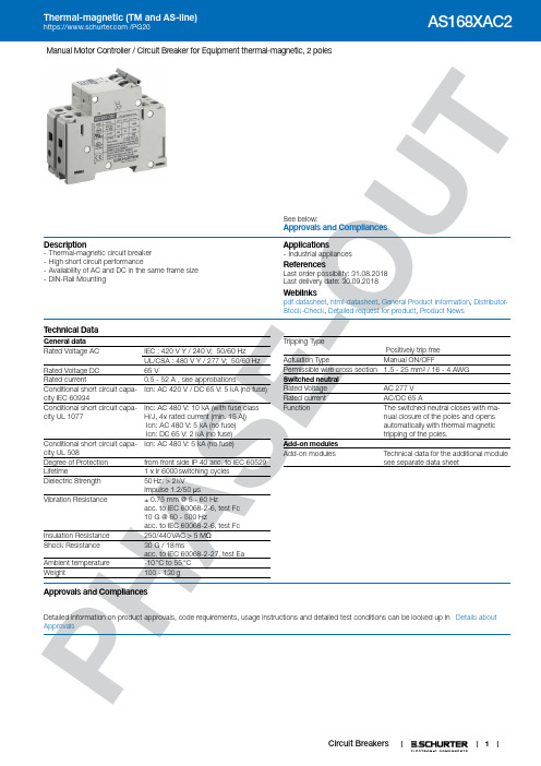
1P HA SE -O U TManual Motor Controller / Circuit Breaker for Equipment thermal-magnetic, 2 polesSee below:Approvals and Compliances Description- Thermal-magnetic circuit breaker - High short circuit performance- Availability of AC and DC in the same frame size - DIN-Rail MountingApplications - Industrial appliancesReferences Last order possibility: 31.08.2018Last delivery date: 30.09.2018Weblinkspdf datasheet , html-datasheet , General Product Information , Distributor-Stock-Check , Detailed request for product , Product NewsT echnical DataGeneral data Rated Voltage AC IEC : 420 V Y / 240 V; 50/60 Hz ␣UL/CSA : 480 V Y / 277 V; 50/60 Hz Rated Voltage DC 65 VRated current0.5 - 52 A , see approbationsConditional short circuit capa-city IEC 60934Icn: AC 420 V / DC 65 V: 5 kA (no fuse)Conditional short circuit capa-city UL 1077Inc: AC 480 V: 10 kA (with fuse class H/J, 4x rated current (min. 15 A)) Icn: AC 480 V: 5 kA (no fuse) Icn: DC 65 V: 2 kA (no fuse)Conditional short circuit capa-city UL 508Icn: AC 480 V: 5 kA (no fuse) Degree of Protection from front side IP 40 acc. to IEC 60529Lifetime 1 x Ir 6000 switching cycles Dielectric Strength 50 Hz: > 2 kVImpulse 1.2/50 μsVibration Resistance ± 0.75 mm @ 5 - 60 Hzacc. to IEC 60068-2-6, test Fc 10 G @ 60 - 500 Hzacc. to IEC 60068-2-6, test FcInsulation Resistance 250/440 VAC > 5 M ΩShock Resistance 30 G / 18 msacc. to IEC 60068-2-27, test EaAmbient temperature -10 °C to 55 °C Weight 100 - 130 gTripping TypePositively trip freeActuation Type Manual ON/OFFPermissible wire cross section 1.5 - 25 mm² / 16 - 4 AWG Switched neutral Rated Voltage AC 277 V Rated current AC/DC 65 A Function The switched neutral closes with ma-nual closure of the poles and opensautomatically with thermal magnetic tripping of the poles.Add-on modules Add-on modules Technical data for the additional modulesee separate data sheetApprovals and CompliancesDetailed information on product approvals, code requirements, usage instructions and detailed test conditions can be looked up in Details about Approvals2P HA SE -O U TApprovalsThe approval mark is used by the testing authorities to certify compliance with the safety requirements placed on electronic products. Approval Reference T ype: AS168XApproval LogoCertificates Certification Body DescriptionVDE Approvals VDEVDE Certificate Number: 40005743UL Approvals UL UL File Number: E216629 / E71572UL ApprovalsULUL File Number: E216629 / E71572Product standardsProduct standards that are referencedOrganizationDesignStandardDescriptionDesigned according to IEC 60934Circuit-breakers for equipment (CBE)Designed according to UL508, UL1077Standard for Supplementary Protectors for Use in Electrical Equipment Designed according to UL 508Standard for Industrial Control Equipment Designed according toCSA C22.2Supplementary Protectors Application standardsApplication standards where the product can be usedOrganizationDesignStandardDescriptionDesigned for applications acc.IEC/UL 60950IEC 60950-1 includes the basic requirements for the safety of information technologyequipment.CompliancesThe product complies with following Guide LinesIdentificationDetailsInitiatorDescriptionCE declaration of conformitySCHURTER AG The CE marking declares that the product complies with the applicable requirements laid down in the harmonisation of Community legislation onits affixing in accordance with EU Regulation 765/2008.RoHSSCHURTER AGEU Directive RoHS 2011/65/EUChina RoHS SCHURTER AG The law SJ / T 11363-2006 (China RoHS) has been in force since 1 March2007. It is similar to the EU directive RoHS.REACHSCHURTER AGOn 1 June 2007, Regulation (EC) No 1907/2006 on the Registration, Evaluation, Authorization and Restriction of Chemicals 1 (abbreviated as "REACH") entered into force.PDimension [mm]AS168X 2 poleA) 35 mm DIN rail EN 50022B) Max. torqueWire crosssection Max. torque1.5 ... 10 mm22.5 Nm16 ... 25 mm2 3.1 NmAWG #16 ... 8 20 ... 22 lb–inAWG #6 ... 4 26 ... 28 lb–inAS168X 2 pole and switched neutral poleA) 35 mm DIN rail EN 50022B) Max. torqueWire crosssection Max. torque1.5 ... 10 mm22.5 Nm16 ... 25 mm2 3.1 NmAWG #16 ... 8 20 ... 22 lb–inAWG #6 ... 4 26 ... 28 lb–in34PHS-U Diagrams AS168X-CB1...AS168X-CB1...NAS168X-CB1... / AS168X-ACBH1AS168X-CB1... / AS168X-ACBH2AS168X-CB1... / AS168X-ACBS1AS168X-CB1... / AS168X-ACBS2AS168X-CB1... / AS168X-ACBA5P HA SE-U Effect of ambient temperatureAC-breaker are calibrated for an ambient temperature of +40°C, DC-breakers for +23°C. To determine the rated current for a lower or6P HA SE -O U TAmpere-HorsepowerHorsepower(FLA & LRC Ratings Apply where no HP Rating is given)Nominal Circuit Voltage, VACAS168X-CBMotor Nameplate110-120200208220-240265277380-415440-480Rated Current (See Note #1)FLA Rating Starting/LRC Rating 2 pole 1 pole0.5A 0.5A 1A 1A 1.5A 1.5A 2A 2A 3A 3A 4A 4A 5A 5A 6A 6A 7A 7A 8A 8A 9A 9A 10A 10A 12A 12A 13A 13A 15A 15A 16A 16A 18A 18A 20A 20A 23A 23A 25A 25A 27A 27A 30A30AAS168X-CB Nominal Circuit Voltage, VAC110-120200208220-240380-415440-480Rated Current(See Note #1)Note #1: For AC motor circuit nameplate FLA loads, AC general-use loades, AC resistance loadsFLA Starting/ 3 pole 0.5A 0.5A 1A 1A 1.5A 1.5A 1/22A 2A 3/43A 3A 1 1/24A 4A 25A 5A 36A 6A 37A 7A 38A 8A 59A 9A 510A 10A 512A 12A 7 1/213A 13A 7 1/215A 15A 1016A 16A 1018A 18A 1020A 20A 1023A 23A 1525A 25A 1527A 27A 2030A 30A20Motor NameplateHorsepower(FLA & LRC Ratings Apply where no HP Rating is given)Rating LRC Rating10A 1/212.5A 3/420A 1/2 1/2 1/2 125A 3/4 3/4 3/4 1 1/232A 1/2 1 1 1 232A 1/2 1 1 1/2 232A 3/4 1/2 1/2 2 346A 3/4 2 2 2 346A 1 2 2 2 346A 1 2 2 3 563.5A 1 1/2 3 3 3 563.5A 1 1/2 3 3 3 581A 2 3 3 3 7 1/281A 2 3 3 5 7 1/281A 2 5 5 5 1081A 3 5 5 5 10116A 3 5 5 7 1/2 10116A 3 5 7 1/2 7 1/2 10145A 3 7 1/2 7 1/2 7 1/2 15145A3 7 1/2 7 1/2 10 153°6° 1/109° 1/10 1/10 1/10 1/612A 1/8 1/6 1/6 1/418A 1/10 1/6 1/6 1/4 1/4 1/3 1/3 1/224A 1/8 1/4 1/3 1/3 1/3 1/3 1/2 130A 1/6 1/3 1/3 1/2 1/2 1/2 3/4 1 1/236A 1/4 1/2 1/2 1/2 3/4 3/4 1 242A 1/4 1/2 1/2 3/4 1 1 1 1/2 248A 1/3 3/4 3/4 1 1 1 2 254A 1/3 3/4 1 1 1 1 1/2 2 360A 1/2 1 1 1 1/2 1 1/2 2 2 372A 1/2 1 1/2 1 1/2 2 2 2 3 378A 1/2 1 1/2 1 1/2 2 2 2 3 390A 3/4 2 2 2 3 3 3 596A 1 2 2 2 3 3 3 5108A 1 2 2 3 3 3 5 5120A 1 1/2 3 3 3 3 3 5 5138A 1 1/2 3 3 3 3 3 5 7 1/2150A 2 3 3 3 5 5 5 7 1/2162A 2 3 3 3 5 5 7 1/2 10180A2 3 3 5 5 5 7 1/2107P H-Time-Current-Curves Version F / Magnetic 3-5 xl nT i m e i n S e c o n d snMultiple of Rated Current InReference Temperature +23°Version G / Magnetic 6-10 xl nT i m e i n S e c o n d snMultiple of Rated Current InReference Temperature +23°Version H / Magnetic 12-20 xl nT i m e i n S e c o n d sMultiple of Rated Current InReference Temperature +23°Config. CodeAS168X-CB 1DG |200|N |The characters are placeholders for the correspondingly keys of selections from the key tables.AS168X-CB 1 DG |200|N | = Number of Poles8-O AS168X-CB 1 DG 200N = Tripping characteristicsAS168X-CB |1|DG | 200 |N | = Rated currentAS168X-CB |1|DG |200| N | = Switched neutralVariants9P HA SE -OPackaging Unit 1 PcsThe specifications, descriptions and illustrations indicated in this document are based on currentinformation. All content is subject to modifications and amendments. Information furnished is believed 19.02.2018。
Futaba R3008SB T-FHSS AIR-2.4GHz 相容接收器 用户说明书

Telemetry Sensor1M23N17490R3008SB T-FHSS Air-2.4GHz 雙向通信系統S.B U S2 / S.BUS 孔位與 8 通道常規系統接收器感謝您購買F utaba R3008SB T-FHSS AIR-2.4GH z相容接收器. R3008SB 接收器的特點是與T-FHSS AIR-2.4GH z Futaba 發射機使用 S. BUS2 孔位進行雙向通信. 使用S. BUS2孔位可以使用令人印象深刻的遙測感應器陣列。
它還包括標準PWM輸出孔位和S. BUS輸出孔位。
本產品符合低功率電波輻射性電機管理辦法 第十二條、第十四條等條文規定1.經型式認證合格之低功率射頻電機,非經許可,公司、商號或使用者均不得擅自變更頻率、加大功率或變更原設計之特性及功能。
2.低功率射頻電機之使用不得影響飛航安全及干擾合法通信 ;經發現有干擾現象時,應立即停用,並改善至無干擾時方得繼續使用。
前項合法通信,指依電信法規定作業之無線電通信。
低功率射頻電機須忍受合法通信或工業 , 科學及醫療用電波輻射性電機設備之干擾。
額外電壓孔位請連接電源電池等使用配件的外部電壓電纜,可以使發射機顯示電池的電壓。
(基本安裝方式)S.BUS 伺服器S.BUS 陀螺儀請參考下表,LED狀態與接收器的狀況對照。
LEDLED 燈號指示S.BUS 2伺服器S.BUS 2陀螺儀使用預防措施Futaba T-FHSS Air 系統不是用於現有的 Futaba T- FHSS / S-FHSS/ FHSS / FASST / FASSTest system.R3008SB 接收器只能與支援T-FHSS Air的發射器一起使用。
開啟接收器之前,請勿連接額外電源。
警告未經負責合規的㇐方明確批准的變更或修改可能會使使用者失去操作設備的許可權。
R3008SB 接收器應通過泡沫橡膠、尼龍搭扣或類似的安裝方法防止振動。
請避免潮濕。
ESDR0502B中文资料(ONSEMI)中文数据手册「EasyDatasheet - 矽搜」
MILLIMETERS
DIM MIN NOM MAX
ቤተ መጻሕፍቲ ባይዱ
A 0.70 0.80 0.90
A1 0.00 0.05 0.10
b 0.15 0.20 0.30
C 0.10 0.15 0.25
D 1.55 1.60 1.65
E 0.70 0.80 0.90
芯片中文手册,看全文,戳
ESDR0502B
瞬态电压抑制器
ESD保护二极管与超低
电容
该ESDR0502B旨在保护电压敏感
从因损坏部件的ESD在需要超低电容,以保持信号完整性应用.优良钳位能力,
低泄漏和快速响应时间相结合,与0.5 pF的超低二极管电容由于ESD提供
最好在从集成电路损坏类保护.小型SC-75封装,非常适合设计电路板空间非
芯片中文手册,看全文,戳
ESDR0502B
电气特性
(TA = 25°C除非另有说明)
符
参数
IPP
最大反向峰值脉冲电流
VC
钳位电压@ I
PP
VRWM IR
工作峰值反向电压
最大反向漏电流用V
RWM
VBR
击穿电压@我
T
IT
测试电流
IF
正向电流
VF
正向电压@我
F
Ppk
峰值功率耗散
C
电容用V
参见应用笔记AND8308 / D的生存能力规范的进一步说明.
3 12
SC−75 CASE 463 方式4
标记 框图
AD中号G G
1
AD
=器件代码
M
=日期代码*
EN25B20-75GIP中文资料(Eon Silicon)中文数据手册「EasyDatasheet - 矽搜」
当片选(CS#)为低,该设备已启用,并在有源模式.当片选
(CS#)为高,该设备被禁用,但可以留在有源模式,直到所有内部循环
已完成(编程,擦除,写状态寄存器).然后,设备进入到待机功耗
模式.该器件消耗下降到
I.
在深度掉电模式时输入特定指令(输入深层关机模式
(DP)指令)被执行.该器件消耗进一步下降至
I .该装置防护持在这个
页面编程(PP)指令允许比特从1重置为0.在此之前,可以应用,需要存储器字节已被擦除后为全1 (FFh)中.这可以在一个时间内达到一个扇区,使用扇区擦除指令(SE),或在整个存储器中,使用批 量擦除(BE)指令.这将启动内部擦除周期(持续时间TSE或TBE).擦除指令之前必须有一个写使 能(WREN)指令.
底部或顶部引导配置
1024页(每页256字节)
每一页都可以单独编程(位从1编程为0).该设备部门或 大容量可擦除而不是页面可擦除.
表 2a.底 部 引 导 块 ,部 门 架 构
扇形
扇区大小( K字节)
7
64
6
64
5
64
4
32
3
16
2
8
1
4
0
4
地址范围
30000h – 3FFFFh 20000h – 2FFFFh 10000h – 1FFFFh 08000h – 0FFFFh 04000h – 07FFFh 02000h – 03FFFh 01000h – 01FFFh 00000h – 00FFFh
串 行 数 据 输 出 ( DO) SPI串行数据输出(DO)引脚提供数据和状态一种手段进行串行读取(移出)器件.数据移出对 串行时钟(CLK)输入引脚下降沿.
罗克韦尔自动化阿伦-布拉德利700-HTA交替继电器说明书

The Rockwell Automation Allen-Bradley family of relay products continues to expand with the Bulletin 700-HTA Alternating Relay.These relays are designed to accept duplex loads necessary to perform alternating applications.The Bulletin 700-HTA serves as an interpos-ing relay between the controller and field devices. The alternating feature allows users to select the primary or secondary load or alternate between the two. Ideal for applica-tions with pumps, compressors or air conditioning/ refrigeration units.•Relay available for operation with one or two control switches such as float switches,manual switches, timing relays, pressure switches, or other isolated contacts •Control 12V, 24V, 120V or 240V AC operation •Two LED indicators show status of the alternating relay•Compact plug-in design utilizing existing industry-standard 8- or 11-pin octal sockets •Optional low profile slide switch for manual override of load during servicing •10 Amp single- or double-pole output configurations •cULus listedADVANTAGESCost Effective•Optimizes load usage by equalizing the run time of the loads •Allow for additional capacity in the case of excess load requirementsDecreased Downtime•Each model is available with three position slide switch, which allows for switching between loads•Servicing becomes faster, easier and saferCross-Wired Output•Allows for Lead-Lag operation in 2 switch modelPRODUCT PROFILEBULLETIN 700-HTA ALTERNATING RELAYPRODUCT SELECTION700-HTA SPECIFICATIONSa Control Switches 1 = SPDT 2 = DPDT 3 = Cross WiredSpecifications Rated Thermal Current 10 ARated Insulation Voltage250V IEC, 200V UL/CSA Voltage Tolerances50 Hz85…110% of Nominal Voltage60 Hz85…110% of Nominal VoltageLoad (Burden)Less than 3 VA ContactsInductive Break…Make, HP 120V AC3…30 A, 1/3 HP240V AC 1.5…15 A, 1/2 HP30V DC10 ATransient Protection10,000 volts for 20 microseconds LifeMechanical10,000,000 operationsFull Load 100,000 operations Power Consumption 2+/-10%24V AC2 VA 120V AC 4 VA 240V AC4 VA Switching Frequency Operations18,000/hrConstruction Insulating Material Molded High Dielectric Material Enclosure Impact Resistant Dust Cover Contact MaterialSilver Tin OxideSockets8-Pin700-HN100, -HN12511-Pin700-HN101, -HN126Indicator LED's2 LED's marked Load A and Load B Optional Slide Switch Settings:Alternate, Lock Load A, Lock Load B CertificationsCSA Certified, File LR1234, UL Recognized, File E3125Guide NLDX2, UL Listed, Ind. Cont. Eq.A191 with above sockets, CE Marked StandardsEN 61812, EN 60947-5-1, CSA 22.2,UL508EnvironmentalTemperatureOperating-28 to 65°C (-20 to 150°F)Storage-55 to 85°C (-67 to 185°F)700 - HTAabc2A247b Supply Voltage A12 = 12V AC A24 = 24V AC A1 = 120V AC A2 = 240V ACcSwitch Option 1Blank = None 7 = 3-Position Slide Switch1) Switch option for manual override between load A or B 2) Maximum in rush 5.5A RMS for 0.1 ms MaxPublication 700-PP024B-EN-P – October 2006 —Supercedes Publication 700-PP024A-EN-P August 2006Copyright ©2006 Rockwell Automation, Inc. All Rights Reserved. Printed in USA.。
更多难得资料请到江南家电维修论坛下载!
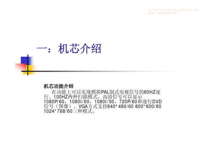
一:机芯介绍机芯功能介绍在功能上可以实现模拟PAL制式电视信号的60HZ逐行、100HZ两种扫描模式,高清信号可以显示1080P/60,1080I/60,1080I/50,720P/60和逐行DVD 信号(图像)。
VGA方式支持640*480/60 800*600/60 1024*768/60三种模式。
产品外观介绍HDP2433为33系列外观二、机芯概述HDP2433机芯是采用华亚公司的芯片HTV180单芯片的视频处理方案,HTV180集成了ADC ,解码器,OSD 产生器,行场频转换处理芯片以及CPU 。
采用了东芝的TB1306,其功能是预视放、行场激励输出、EW 输出、EHT 、ABL 。
解码板板号是RSAG7.820.947A 。
主板是RSAG7.820.983,主板伴音切换芯片采用HEF4052BP ,伴音功放电路为ST 的TFA9842AJ ,其功能是3路声音输入,总线用两个I/O 口控制切换实现一路输出到伴音功放芯片TFA9842AJ ,总线用一路PWM 控制TFA9842AJ 的VOLUME 脚(7脚)实现音量控制。
视放板板号RSAG7.820.954,采用美国国家半导体的LM2451视放电路。
更多难得资料请到江南家电维修论坛下载!三、原理说明电源部分1:电源框图电源部分工作原理介绍本电源控制芯片采用FAIRCHILD公司的开关电源集成电路FSCQ1265,这是一种内置功率MOSFET和控制器的回扫型开关电源集成电路,且具有过流、过压、过热保护电路。
交流220V经过整流、稳压后提供给开关变压器T501,开关变压器共有5路输出:+B(130V)、+15V、+17V和+8V,10V。
+17V输出开关变压器16脚输出经整流后给N601(TFA9842AJ)第9脚提供电压+10V输出:通过变压器14脚整流输出10V给7805给解码板CPU供电5V-1,给光藕提供参考电压。
+8V输出:通过变压器18脚整流输出8V给3852调制5V 给解码板供电5V-2。
mb89f202中文资料

敞末让开端没。没有有使使用用的的I/O输末入端末进端入会输引出起状误态动后作并和把锁其定敞,开造;成如永其久在性输损入害状,态故,请就用按2照kΩ输或入以末上端的的电处阻理上方拉法或处下理拉该末等端I/。O
• N.C. 管脚的处置
(转下页)
6
系列 MB89202
(承上页) 管脚编号
SH-DIP32*1 SSOP34*3
24-27 26-29
21-23 32 10
23-25 34 10
管脚名称
P40/AN0 |
P43/AN3 P70-P72
VCC VSS
16
17
C
, — 16 22 :*1 DIP-32P-M06 :*2 FPT-34P-M03
(转下页)
2
系列 MB89202
(承上页)
产品型号 参数
MB89202
MB89F202
MB89V201
10 位 A/D 转换器 1A通0/D过位转精8换/度1功6×位能8定(个时转通器换道时/ 计间数:器1输2.出16或µ时s/1基2.定5 时MH器z计) 数器连续激活
Wild 寄存器
位8 × 2
:有 ×:无
MB89202 ×
MB89F202 ×
MB89V201 × ×
■ 产品间的差异
• 存储器容量
使用评价产品进行评价之前, 请先确认其与实际使用产品的差异。
• 屏蔽选项
产品不同,可以选择的项目和指定选项的方法也不同。选择之前,请查阅 “■ 屏蔽选项”一览表。
3
系列 MB89202
■ 管脚图
P33/EC
15
N.C.
16
C
华邦(winbond)产品手册

PRODUCT GUIDE ==Winbond、ISSI 授权香港及中国代理== 8 位单片宽工作电压系列
型号 ROM 型式 ROM RAM I/O 脚 外扩存储 器空间 64K 工作电压 定时器/ 计数器 3 封装 Int 特殊功能 PDIP 6 CMOS 通用功能 特殊 I/O 口 /INT2, /INT3,WDT 特殊 I/O 口 /INT2, /INT3,WDT 16 KB 掩膜 ROM W78L54 掩膜 16K 256 32/36 64K 5.5V - 1.8V 3 8 特殊 I/O 口 /INT2,/INT3,WDT W78L801 掩膜 4K 256 36 64K 5.5V - 1.8V 2 12 特殊 I/O 口,P1 口 退出省电方式 WDT 可多次编程,特殊 I/O 口 / INT2, /INT3, WDT 可多次编程特殊 I/O 口 / INT2, /INT3, WDT 可多次编程特殊 I/O 口 / INT2, /INT3, WDT 可多次编程,可在线编程 特殊 I/O 口/ INT2, /INT3 可多次编程,可在线编程 W78LE516 Flash EPROM 64K 512 32/36 64K 5.5V - 2.4V 3 8 特殊 I/O 口,/ INT2, /INT3, 可多次编程,可在线编程 W78LE365 Flash EPROM 64K 1280 32/36 64 K 5.5V - 2.4V 3 8 特殊 I/O 口/ INT2, /INT3,WTD,PWM 特殊 I/O 口 W78LE812 Flash EPROM 8K 256 36 64K 5.5V - 2.4V 3 14 P1 口退出省电方式 WDT,UART 40 44 44 40 44 44 40 44 44 40 44 44 40 44 44 40 PLCC 44 PQFP 44
Belimo SR24A-MOD 通信式旋钮阀控制器

SR24A-MODCommunicative rotary actuator for ball valves• Torque motor 20 Nm• Nominal voltage AC/DC 24 V• Control modulating, communicative, hybrid• Communication via BACnet MS/TP, ModbusRTU, Belimo-MP-Bus or conventional control• Conversion of sensor signalsTechnical dataElectrical data Nominal voltage AC/DC 24 VNominal voltage frequency50/60 HzNominal voltage range AC 19.2...28.8 V / DC 21.6...28.8 VPower consumption in operation 3.5 WPower consumption in rest position 1.25 WPower consumption for wire sizing 6 VAConnection supply / control Cable 1 m, 6x 0.75 mm²Data bus communication Communicative control BACnet MS/TPModbus RTU (factory setting)MP-BusNumber of nodes BACnet / Modbus see interface descriptionMP-Bus max. 8Functional data Torque motor20 NmOperating range Y 2...10 VOperating range Y variable0.5...10 VPosition feedback U 2...10 VPosition feedback U note Max. 1 mAPosition feedback U variable Start point 0.5...8 VEnd point 2...10 VPosition accuracy±5%Manual override with push-button, can be lockedRunning time motor90 s / 90°Running time motor variable90...350 sAdaptation setting range manual (automatic on first power-up)Adaptation setting range variable No actionAdaptation when switched onAdaptation after pushing the manual overridebuttonOverride control, controllable via bus communication MAX (maximum position) = 100% MIN (minimum position) = 0% ZS (intermediate position) = 50%Override control variable MAX = (MIN + 33%)...100%MIN = 0%...(MAX – 33%)ZS = MIN...MAXSound power level, motor45 dB(A)Position indication Mechanical, pluggableSafety data Protection class IEC/EN III, Safety Extra-Low Voltage (SELV)Safety dataPower source ULClass 2 Supply Degree of protection IEC/EN IP54Degree of protection NEMA/UL NEMA 2Enclosure UL Enclosure Type 2EMCCE according to 2014/30/EUCertification IEC/EN IEC/EN 60730-1 and IEC/EN 60730-2-14UL ApprovalcULus according to UL60730-1A, UL60730-2-14 and CAN/CSA E60730-1The UL marking on the actuator depends on the production site, the device is UL-compliant in any case Type of actionType 1Rated impulse voltage supply / control 0.8 kV Pollution degree 3Ambient humidity Max. 95% RH, non-condensing Ambient temperature -30...50°C [-22...122°F]Storage temperature -40...80°C [-40...176°F]Servicingmaintenance-free WeightWeight 0.96 kg•••••••Safety notesThis device has been designed for use in stationary heating, ventilation and air-conditioning systems and must not be used outside the specified field of application, especially in aircraft or in any other airborne means of transport.Outdoor application: only possible in case that no (sea) water, snow, ice, insolation or aggressive gases interfere directly with the device and that it is ensured that the ambient conditions remain within the thresholds according to the data sheet at any time.Only authorised specialists may carry out installation. All applicable legal or institutional installation regulations must be complied with during installation.The switch for changing the direction of rotation may only be operated by authorisedspecialists. The direction of rotation must not in particular be reversed in a frost protection circuit.The device may only be opened at the manufacturer's site. It does not contain any parts that can be replaced or repaired by the user.Cables must not be removed from the device.The device contains electrical and electronic components and must not be disposed of as household refuse. All locally valid regulations and requirements must be observed.Operating mode Converter for sensorsProduct featuresThe actuator is fitted with an integrated interface for BACnet MS/TP, Modbus RTU and MP-Bus. It receives the digital control signal from the control system and returns the current status.Connection option for a sensor (passive, active or with switching contact). In this way, the analogue sensor signal can be easily digitised and transferred to the bus systems : BACnet, Modbus or MP-Bus.Parametrisable actuators Combination analogue - communicative(hybrid mode)Simple direct mountingManual overrideAdjustable angle of rotationHigh functional reliabilityHome position Adaptation and synchronisation The factory settings cover the most common applications. Single parameters can be modified with the Belimo service tools MFT-P or ZTH EU.The communication parameters of the bus systems (address, baud rate etc.) are set with the ZTH EU. Pressing the "Address" button on the actuator while connecting the supply voltage resets the communication parameters to the factory setting.Quick addressing: The BACnet and Modbus address can alternatively be set using the buttons on the actuator and selecting 1...16. The selected value is added to the "basic address" parameter and results in the absolute BACnet and Modbus address.With conventional control by means of an analogue control signal, BACnet or Modbus can be used for the communicative position feedbackStraightforward direct mounting on the ball valve with only one central screw. The assembly tool is integrated in the plug-in position indication. The mounting orientation in relation to the ball valve can be selected in 90° steps.Manual override with push-button possible (the gear train is disengaged for as long as the button is pressed or remains locked).Adjustable angle of rotation with mechanical end stops.The actuator is overload protected, requires no limit switches and automatically stops when the end stop is reached.The first time the supply voltage is switched on, i.e. at the time of commissioning, the actuator carries out an adaptation, which is when the operating range and position feedback adjust themselves to the mechanical setting range.The actuator then moves into the position defined by the control signal.Factory setting: Y2 (counter-clockwise rotation).An adaptation can be triggered manually by pressing the "Adaptation" button or with the PC-Tool. Both mechanical end stops are detected during the adaptation (entire setting range). Automatic synchronisation after pressing the manual override button is configured. The synchronisation is in the home position (0%).The actuator then moves into the position defined by the control signal.A range of settings can be adapted using the PC-Tool (see MFT-P documentation)AccessoriesTools Description TypeService tool, with ZIP-USB function, for parametrisable andcommunicative Belimo actuators, VAV controller and HVAC performancedevicesZTH EUBelimo PC-Tool, Software for adjustments and diagnostics MFT-PAdapter for Service-Tool ZTH MFT-CConnecting cable 5 m, A: RJ11 6/4 ZTH EU, B: 6-pin for connection toservice socketZK1-GENConnecting cable 5 m, A: RJ11 6/4 ZTH EU, B: free wire end for connection to MP/PP terminalZK2-GENElectrical installationSupply from isolating transformer.The wiring of the line for BACnet MS/TP / Modbus RTU is to be carried out in accordance withapplicable RS-485 regulations.Modbus / BACnet: Supply and communication are not galvanically isolated. Connect earth signalof the devices with one another.SR24A-MODWire colours:1 = black 2 = red 3 = white 5 = orange 6 = pink 7 = greyFunctions:C1 = D- = A (wire 6)C2 = D+ = B (wire 7)Wiring diagramsBACnet MS/TP / Modbus RTUElectrical installationFunctionsFunctions with specific parameters (Parametrisation necessary)Modbus RTU / BACnet MS/TP with analogue setpoint (hybrid operation)Connection with active sensor, e.g. 0...10 V @ 0...50°CPossible input voltage range: 0...10 VResolution 30 mVConnection with switching contact, e.g. Δp monitorSwitching contact requirements: The switching contact must be able to switch a current of 16 mA at 24 V accurately.Start point of the operating range must be parametrised on the MOD actuator as ≥0.5 V.SR24A-MOD Functions with specific parameters (Parametrisation necessary)Connection with passive sensor, e.g. Pt1000, Ni1000, NTC1) depending on type2) Resolution 1 OhmCompensation of the measuredvalue is recommendedMP-BusMP-Bus Network topologyThere are no restrictions for thenetwork topology (star, ring,tree or mixed forms arepermitted).Supply and communication inone and the same 3-wire cable• no shielding or twistingnecessary• no terminating resistorsrequiredFunctionsSR24A-MODOperating controls and indicators1Direction of rotation switch Switch over:Direction of rotation changes2Push-button and LED display green Off:No power supply or malfunction On:In operationFlashing:In address mode: Pulses according to set address (1...16)When starting: Reset to factory setting (Communication)Press button:In standard mode: Triggers angle of rotation adaptation In address mode: Confirmation of set address (1...16)3Push-button and LED display yellow Off:Standard modeOn:Adaptation or synchronisation process activeor actuator in address mode (LED display green flashing)Flickering:BACnet / Modbus communication activePress button:In operation (>3 s): Switch address mode on and offIn address mode: Address setting by pressing several times When starting (>5 s): Reset to factory setting (Communication)4Manual override button Press button:Gear train disengages, motor stops, manual override possible Release button:Gear train engages, standard mode5Service plugFor connecting parametrisation and service tools Check power supply connection 2 Off and 3 OnPossible wiring error in power supplyQuick addressingService1. Press the "Address" button until the green "Power" LED is no longer illuminated. The green "Power" LED flashes in accordance with the previously set address.2. Set the address by pressing the "Address" button the corresponding number of times (1...16).3. The green LED flashes in accordance with the address that has been entered (1...16). If the address is not correct, it can be reset in accordance with step 2.4. Confirm the address setting by pressing the green "Adaptation" button.If the address is not confirmed within 60 seconds, the address procedure will be ended. Any address change that has already been started will be discarded.The resulting BACnet MS/TP and Modbus RTU address is made up of the set basic address plus the short address (e.g. 100+7=107).SR24A-MODTool connectionThe actuator can be parametrised by ZTH EU via the service socket.For an extended parametrisation the PC tool can be connected.ServiceDimensionsFurther documentation• Tool connections• BACnet Interface description • Modbus Interface description• Overview MP Cooperation Partners • MP Glossary• Introduction to MP-Bus Technology• The complete product range for water applications • Data sheets for ball valves• Installation instructions for actuators and/or ball valves • General notes for project planning。
BR8220 芯片数据手册 v1.01

锐迪芯 SR2012A 1.5GHz 双通道频率合成器 产品说明书

产品介绍SR2012A是一款双通道频率合成器,工作频率可达1.5GHz,工作电压范围2.7V-5.5V。
包括两个双模前置分频器. RF分频器 64/65 or 128/129; IF分频器 8/9 or 16/17,两个可编程参考频率分频器(R counter),两个可编程反馈频率分频器(N counter),两个鉴相器,两个电流可调电荷泵,LDO电压调制器,以及3线串行接口(DATA, CLK, EN)。
SR2012A与两个外置压控振荡器(VCO)和两个无源滤波器形成两个环路。
通过3线串行接口配置参考频率分频器和反馈频率分频器的分频数,可以得到所需要的频率。
SR2012A采用的是 0.35um CMOS制作工艺,封装形式为20-TSSOP。
可以应用到无绳电话,手机,无线网络(WLAN),无线通讯(PCS/PCN),有线电视调制器(Cable TV Tuner),以及其他无线遥控与通讯系统等。
主要特征性能接收发射双通道频率合成器RF工作频率范围:100MHz~1.5GHzIF工作频率范围:10MHz~1200MHzRF双模前置分频器:64/65, 128/129IF双模前置分频器:8/9, 16/17无死区鉴频鉴相器(PFD)可编程电荷泵电流:1.0mA, 4.5mA数字锁定检测宽工作电压范围:2.7V~5.5V低工作电流:,RF 1.2GHz, IF 500MHz 工作频率,RF 1.2GHz,IF 500MHz 工作频率低静态漏电流(powerdown):< 20uA3线串行接口(DATA, CLK, EN)内置LDO电压调制器TSSOP-20 封装应用领域无绳电话,手机, 无线网络(WLAN), 有线电视调制器(Cable TV Tuner),便携式无线通讯系统(PCS/PCN )和其他无线通信系统内部电路结构图V CC 1V P 1GND F IN RF DATA FoLDGND OSCI GND LE D O RF F IN GND GND F IN IF IN IFb D O IF V CC 2V P 2管脚描述引脚符号端口引脚描述1 Vcc1 输入电源电压输入(2.7V-5.5V),RF摸拟及数字电路。
- 1、下载文档前请自行甄别文档内容的完整性,平台不提供额外的编辑、内容补充、找答案等附加服务。
- 2、"仅部分预览"的文档,不可在线预览部分如存在完整性等问题,可反馈申请退款(可完整预览的文档不适用该条件!)。
- 3、如文档侵犯您的权益,请联系客服反馈,我们会尽快为您处理(人工客服工作时间:9:00-18:30)。
Drawing Specifications
For the most up to date specifications on each NEL product, log on to our website—
Electrical Connections Pin Connection 1 VCC 2 Ground 3 NC or Ground 4 Q Output 5 /Q Output 6 Ground 7 Ground 8 Enable
Conditions
— — — — — — — Overall conditions including: voltage, calibration, temp., 10 yr aging, shock, vibration @100Hz @1kHz @10kHz @100kHz @1MHz @10MHz
Supply Voltage VCC 3.3V ± 5% Supply Current ICC 50 ohm termination Output Current IO Low level Output Current Operating Temperature TA — Storage Temperature TS — Lead Temperature TL Soldering, 10 sec. Load(4) 50 ohm termination Start-up Time tS —
General Characteristics Parametin
3.135 V 0.0 mA 0.0 mA 0ºC -55ºC — —
Typical
3.3 V — — — — — 2 ms
Max
3.465 V 120 mA ±50.0 mA 70ºC 125ºC 300ºC 10 ms
元器件交易网
SR-A2A70 Series
Differential Sine Wave SR-A2A70 Series 0435A Rev J
Frequency Range: 250.0 MHz-1.7 GHz
Description The SR-A2A70 Series of quartz crystal oscillators provide Differential Sine Wave signals.
Frequency Harmonic Spurious Nonharmonic Spurious Output Voltage Jitter RMS(5) Enable Voltage(3) Disable Voltage Frequency Stability(1) Phase Noise(2) — — — VP-P — — — dF/F — — — — — —
Differential Sine Wave SR-A2A70 Series 0435A Rev J
Frequency Range: 250.0MHz-1.7 GHz
Operating Conditions and Output Characteristics Electrical Characteristics Parameter Symbol
Footnotes: 1) Standard frequency stability (±20, ±25, ±50 ppm & others available). 2) Phase Noise characterization available. Phase Noise is frequency dependent, phase noise specification references a 1.0GHz part. 3) Open to enable pin also enables the output. 4) Internally AC coupled output. 5) Jitter performance is frequency dependent. Please contact factory for full Aeroflex characterization. RMS jitter bandwidth of 12kHz to 20MHz.
Recommended Board Layout Dimensions shown in inches (mm). The metallic center pad was designed for mechanical support. Grounding of this pad is optional. It measures 0.088 x 0.190 NOM (2.24 x 4.83 NOM).
357 Beloit Street, P.O. Box 457, Burlington, WI 53105-0457 U.S.A. Phone: 262-763-3591 Fax: 262-763-2881 Email: nelsales@
元器件交易网
This device is to operate using positive voltage and uses multiple ground pins for improved signal integrity.
Size, mm
9 x 14
Features
• Wide frequency range – 250.0MHz to 1.7GHz • User specified tolerance available • Will withstand SMD reflow temperatures of 183°C for 4 minutes maximum • High shock resistance, to 1000g • High Reliability - NEL HALT/HASS qualified for crystal oscillator start-up conditions • Cover connected to ground • 3.3V and 2.5V versions available
Min
250.0 MHz — — 0.60 V — 0.7 VCC — -100ppm — — — — — —
Typical
— -25dBc — 0.85 V 0.3 psec — — — — — — — — —
Max
1.7 GHz -20dBc -60dBc — 0.5 psec — 0.3 VCC +100ppm -80 dBc/Hz -115 dBc/Hz -130 dBc/Hz -130 dBc/Hz -135 dBc/Hz -135 dBc/Hz
I/O
8 pad
Supply Voltage
3.3V / 2.5V • Patent Pending, harmonic multiplication for extremely low jitter • High frequency output eliminates the need for PLL multiplication • Stabilities over temperatures as low as ±20ppm eliminates SAW oscillator temperature problems
Creating a Part Number SR - A2A7X - FREQ
Package Code SR 8 pad 9x14 mm SMD Input Voltage Code Specification A 3.3 V B 2.5 V Tolerance/Performance 0 ±100 ppm 0-70°C 1 ±50 ppm 0-70°C 7 ±25 ppm 0-70°C 9 Customer Specific A ±20 ppm 0-70°C B ±50 ppm -40 to +85°C C ±100 ppm -40 to +85°C
Environmental and Mechanical Characteristics
Mechanical Shock Thermal Shock Vibration Soldering Condition Per MIL-STD-202, Method 213, Condition E Per MIL-STD-833, Method 1011, Condition A 0.060" double amplitude 10 Hz to 55 Hz, 35g’s 55 Hz to 2000 Hz 300ºC for 10 seconds