A215822A2NCNQE中文资料
A22A中文资料
Connected Terminals
Up
Center Down
Slot
Slot
Throw & Schematics
Note: Terminal numbers are not actually on the switch.
OFF NONE
ON
OPEN OPEN
3-1
ON ON ON (ON) (ON) ON (ON)
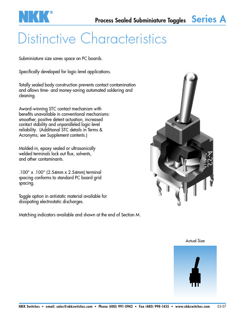
Actual Size
NKK Switches • email: sales@ • Phone (480) 991-0942 • Fax (480) 998-1435 • 03-07
元器件交易网
Series A Process Sealed Subminiature Toggles
Standards & Certifications
UL Recognition or CSA Certification: The A Series toggles have not been tested for UL recognition or CSA certification.
These switches are designed for use in a low-voltage, low-current, logic-level circuit. When used as intended in a logic-level circuit, the results do not produce hazardous energy.
.248” (6.3mm) Long Bat Toggle
SPDT ON-NONE-ON Circuit
Vertical PC Terminals
2N2218A中文资料

• Meets MIL 19500 /251• Collector - Base Voltage 75V • Collector - Current 800 mA• Medium Current, Bipolar TransistorMaximum RatingsRATINGSYMBOL VALUE UNIT Collector - Emitter Voltage V CEO 50Vdc Collector - Base Voltage V CBO 75Vdc Emitter - Base VoltageV EBO6Vdc Collector Current - ContinuousI C800mAdc Total Device Dissipation @ T A = 25 °C P D 0.8WATTS Derate above 25 °C4.6mW/°C Total Device Dissipation @ T C = 25 °C P D 3.0WATTS Derate above 25 °C17.0mW/°C Operating Junction&Storage Temperature RangeT J , T stg- 55 to +200°CThermal CharacteristicsCHARACTERISTICSYMBOL MAX UNIT Thermal Resistance, Junction to Ambient R θ JA 217°C/W Thermal Resistance, Junction to CaseR θ JC59°C/WSWITCHING TRANSISTOR JAN, JANTX, JANTXVElectrical Characteristics (T A = 25°C unless otherwise noted)OFF CHARACTERISTIC SYMBOL MIN MAX UNIT Collector - Emitter Breakdown Voltage (1)V(BR)CEO( I C = 10 mA dc, I B = 0 )50Vdc Collector - Base Breakdown Voltage V(BR)CBO( I C = 10 µAdc, I E = 0 )75Vdc Emitter - Base Breakdown Voltage V(BR)EBO( I E = 10 µAdc, I C = 0 ) 6Vdc Collector - Emitter Cutoff Current I CES( V CE = 50 Vdc )10nAdc Collector - Base Cutoff Current I CBO( V CB = 60 Vdc, I E = 0 )10nAdc ( V CB = 60 Vdc, I E = 0, T A = 150 °C )10µAdc Emitter - Base Cutoff Current I EBO( V EB = 4 Vdc )10nAdc ( V EB = 6 Vdc )10µAdc ON CHARACTERISTIC SYMBOL MIN MAX UNIT DC Current Gain h FE( I C = 0.1 mA dc, V CE = 10 Vdc ) (1)30( I C = 1 mA dc, V CE = 10 Vdc ) (1)35150( I C = 10 mA dc, V CE = 10 Vdc ) (1)40( I C = 150 mA dc, V CE = 10 Vdc ) (1)40120( I C = 500 mA dc, V CE = 10 Vdc ) (1)20( I C = 10 mA dc, V CE = 10 Vdc, T J =-55°C) (1)35Collector - Emitter Saturation Voltage V CE(sat)( I C = 150 mAdc, I B = 15 mAdc ) (1)0.3Vdc ( I C = 500 mAdc, I B = 50 mAdc ) (1) 1.0Vdc Base - Emitter Saturation Voltage V BE(sat)( I C = 150 mAdc, I B = 15 mAdc ) (1)0.6 1.2Vdc ( I C = 500 mAdc, I B = 50 mAdc ) (1) 2.0Vdc 1. Pulse Test: Pulse Width ≤ 300 µs, Duty Cycle ≤.2%Electrical Characteristics (T A = 25°C unless otherwise noted)SMALL - SIGNAL CHARACTERISTICS SYMBOL MIN MAX UNIT Output Capacitance C obo( V CB = 10 Vdc, I E = 0, 100kHz ≤ f ≤ 1 MHz )8.0pF Input Capacitance C ibo( V EB = 0.5 Vdc, I C = 0, 100kHz ≤ f ≤ 1 MHz )25pF SWITCHING CHARACTERISTICS SYMBOL MIN MAX UNIT Turn - On Time t on( V CC = 30 Vdc, I C = 150 mAdc,I B1 =15 mAdc) ( See FIGURE 1 )35ns Turn - Off Time t off( V CC = 30 Vdc, I C = 150 mAdc,I B1 = - I B2 = 15 mAdc) ( See FIGURE 2 )300ns Small - Signal AC Characteristics (T A = 25°C)LOW FREQUENCY SYMBOL MIN MAX UNIT Common - Emitter Forward Current Transfer Ratio h fe( I C = 1 mA, V CE = 10 V, f = 1kHz )35HIGH FREQUENCYCommon - Emitter Forward Current Transfer Ratio|h fe|( I C = 20 mA, V CE = 20 V, f = 100 MHz ) 2.512S p i c e M o d e l (based upon typical device characteristics) *1Q2N2218A NPN ( IS = 21.2f XTI = 3.0 EG = 1.11 VAF= 103.8 BF = 90.7 ISE = 3.34p + NE = 2.05 IKF = 1.255 NK = 0.9394 XTB = 1.5 BR = 1.031 ISC = 3.299p + NC = 1.605 IKR =0.8992 RC = 0.0 CJC = 19.4p MJC = 0.3333 VJC = 0.75 + FC = 0.5 CJE=29.6p MJE= 0.3333 VJE = 0.75 TR = 275.0n TF=564.5p + ITF = 1.0 XTF= 0.0 VTF=10.0 )*1. Microsemi Corp. claims no responsibility for misapplication of Spice Model information. Spice modeling should be used as a precursor guide to in-circuit performance. Actual performance is the responsibility of the user/designer.TO-39 CASE OUTLINEDIE OUTLINEFIGURE 1 Saturated Turn-on Time Test CircuitFIGURE 2 Saturated Turn-off Time Test CircuitFIGURE 3FIGURE 4.0001.001.01.11IC COLLECTOR CURRENT (A)255075100125h F E C U R R E N T G A I N255075100125DC CURRENT GAINVCE = 10 Vtyp @ 25Ctyp @ -55C.0001.001.01.11IB, BASE CURRENT (A)0.00.20.40.60.81.0V C E , C O L L E C T O R -E M I T T E R (V )0.00.20.40.60.81.0COLLECTOR SATURATION vs BASE CURRENTTJ = 25 CIC = 500 mAIC = 150 mAFIGURE 5FIGURE 6.001.01.11IB, BASE CURRENT (A)0.500.751.001.25V B E , B A S E -E M I T T E R V O L T A G E (V )0.500.751.001.25BASE SATURATION vs BASE CURRENTTJ = 25 CIC = 150 maIC = 500 ma.01.1110100REVERSE JUNCTION VOLTAGE (V)51015202530J U N C T I O N C A P A C I T A N C E (p F )051015202530JUNCTION CAPACITANCE TJ = 25 C 100 kHz < f < 1 MHzCOBOCIBOFIGURE 7FIGURE 8101001000COLLECTOR CURRENT (mA)10100t o n T I M E (n s )10100SWITCHING TURN - 0N TIMETJ = 25 C IC/IB = 10min.max.50010100COLLECTOR CURRENT (mA)1001000t o f f T I M E (n s )1001000SWITCHING TURN - OFF TIMETJ = 25 C IC/IB = 10min.max.FIGURE 91101001000FREQUENCY MHz.01.11N O R M A L I Z E D G A I N.01.11NORMALIZED GAIN VS FREQUENCY TJ = 25C IC = 20 mA VCE = 20 V。
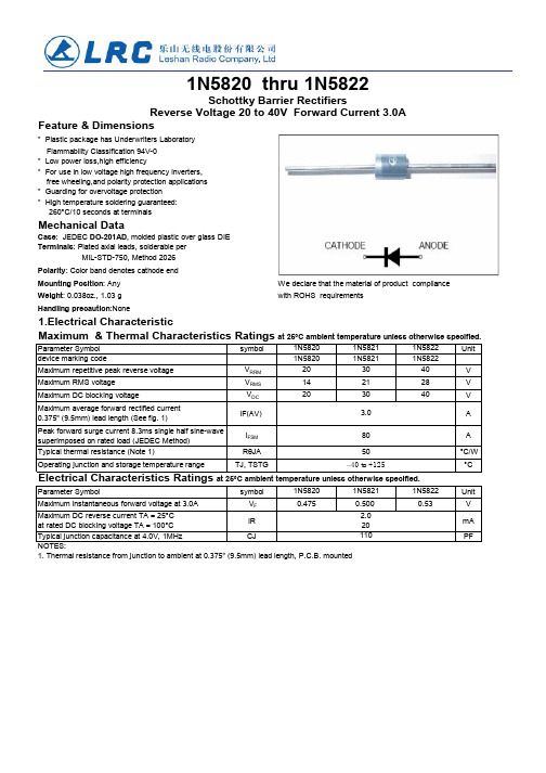
1N5822中文资料_数据手册_参数
Handling precaution:None
1.Electrical Characteristic
Maximum & Thermal Characteristics Ratings at 25°C ambient temperature unless otherwise specified.
Parameter Symbol
Fig 3. – Typical Instantaneous Forward
100
Characteristics
TJ = 25°C Pulse width = 300µs
10 1% Duty Cycle
1.0
0
1
10
100
Number of Cycles at 60Hz
Fig 4. – Typical Reverse Characteristics 10
295±3
W
外箱标签cartoon label
L
3 按以上包装方式,编带数量和外包装箱产品数量:typing and cartoon spec.
每根编带数量 quantity/ammo
A-405 & DO-41 & R-1 3K
外箱数量(T52编带) quantity/cartoon
30K
外箱数量(T26编带)
Parameter Symbol
symbol
1N5820
1N5821
1N5822
Unit
Maximum instantaneous forward voltage at 3.0A
VF
0.475
0.500
Maximum DC reverse current TA = 25°C at rated DC blocking voltage TA = 100°C
1n5822二极管规格书

1n5822二极管规格书
回答:
1n5822二极管是一种超快速恢复二极管,其主要特点是具有高可靠性和高能效。
该二极管的规格书包括以下内容:
1. 最大电压:这是指二极管最大能够承受的正向反向电压。
1n5822二极管的最大正向电压为40V,最大反向电压为40V。
2. 电流:这是指二极管最大能够承受的正向反向电流。
1n5822二极管的最大正向电流为3A,最大反向电流为15uA。
3. 反向恢复时间:这是指二极管从反向导通状态恢复到正向截止状态所需的时间。
1n5822二极管的反向恢复时间为50ns。
4. 功耗:这是指二极管在导通状态下的功率损耗。
1n5822二极管的典型导通功耗为1.5W。
5. 引脚配置:1n5822二极管有两个引脚,分别是阳极和阴极。
阳极标记在上面,阴极标记在下面。
引脚间距为2.54mm。
6. 封装:1n5822二极管的封装为DO-201AD,也叫做DO-27。
其体积为4.8mm x 4.8mm x 9.5mm。
在实际应用中,1n5822二极管广泛应用于电源控制、充电电池保护、逆变器、电动工具等领域。
总的来说,1n5822二极管具有可靠性高、效率高、反向恢复时间短等特点,适用于许多电子电路的应用。
AT24c02最全的中文资料

CA T24C 161/162(16K),CAT24C081 /082(8K) CAT24C041/042(4K),CAT24C021/022(2K)I2C串行CMOS E2PROM,精确的复位控制器和看门狗定时器控制电路特性•数据线上的看门狗定时器(仅对CA T24Cxxl)籲可编程复位门槛电平籲高数据传送速率为400KHz和I2C总线兼容• 2.7V至6V的工作电压•低功耗CMOS工艺籲16字节页写缓冲区籲片内防误擦除写保护籲高低电平复位信号输出——精确的电源电压监视器——可选择5V、3.3V和3V的复位门槛电平•100万次擦写周期•数据保存可长达100年•8脚DIP或SOIC封装•商业级、工业级和汽车温度范围概述CA T24Cxxx是集E2PROM存储器,复位微控制器和看门狗定时器三种流行功能与一体的芯片。
CAT24C161/162 (16K),CAT24C081/082 (8K),CA T24C041/042 (4K)和CAT24C021/022 (2K)以I2C是串行CMOS E2PROM器件。
釆用CMOS工艺大降低了器件的功耗。
CA T24Cxxx 另一特点是16字节的页写缓冲区,提供8脚DIP和SOIC 封装。
CA T24Cxxx的复位功能和看门狗定时器功能保证系统出现故障的时候能给CPU —个复位信号。
CA T24Cxxx 的2脚输出低电平复位信号,7脚输出高电平复位信号。
CAT24Cxxl看狗溢出信号从SDA脚输出。
CAT24Cxx2不具备看门狗功能。
绝对最大参数工作温度:-55°C〜125°C贮存温度:-65°C〜15°C各管脚承受对地电压:-2.0V〜Vcc+2.0V VCC对地电压范围:-2.0V〜7.0V 最大功耗: 1.0W管脚焊接温度(10S): 300 °C输出短路电流:100mA管脚配置]V C C ]RESET方框图表一直流操作特性表二上电时序管脚介绍WP:写保护将该管脚接Vcc,E2PRON就实现写保护(只读)。
A3151U2G2SCNQE中文资料
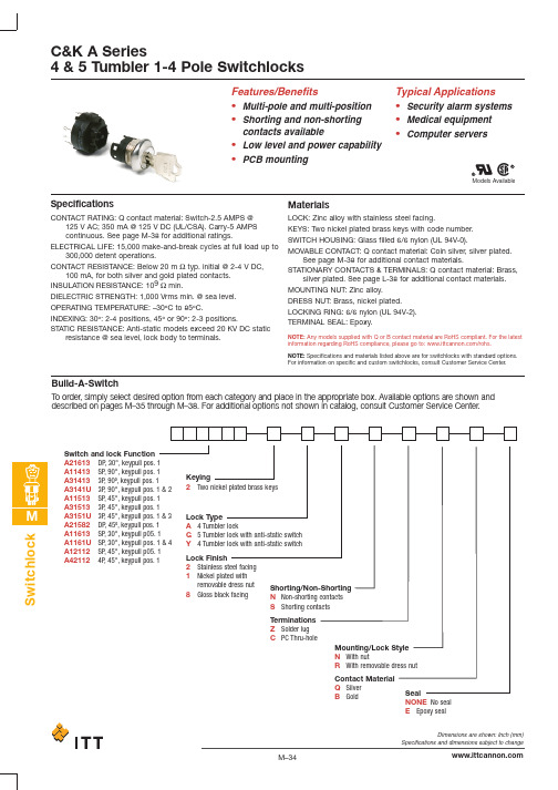
LOCK TYPE A 4 TUMBLER LOCK WITH REMOVABLE DRESS NUT
1.635 (41,52) (4 TUMBLER) 1.733 (44,01) (5 TUMBLER)
.798 (20,26)
.775 (19,68) Key part number: 115140126 NOTE: Key head shape subject to change without notice.
KEYING
OPTION CODE
KEYING OPTIONS
2
2 NICKEL PLATED BRASS KEYS
CODE NO. CODE NO. ON KEY ON LOCK
YES
NO
NOTE: All orders keyed alike, standard. For more than one key code, replacement keys, or other special features, consult Customer Service Center.
Keying 2 Two nickel plated brass keys
A11513 SP, 45°, keypull pos. 1
A31513 3P, 45°, keypull pos. 1
M
A3151U 3P, 45°, keypull pos. 1 & 3 Lock Type
A21582 DP, 45º, keypull pos. 1
STATIC RESISTANCE: Anti-static models exceed 20 KV DC static resistance @ sea level, lock body to terminals.
VIPer12A VIPer22A 中文资料 参数大全
VIPer12A VIPer22A 中文资料参数大全时间:2008-4-25 15:00:46 被阅:18次作者:无VIPower: 采用VIPer22A 的10W 空调开关电源1. 摘要新的空调机采用两个主低压输出给内部电子设备供电。
这两个主输出的低压分别是+12V 和+5V。
低输出电压是由一个内部开关电源产生。
这个开关电源需要以下多个重要特性:效率高,重量轻,尺寸小,待机功耗低等。
设计人员利用VIPerX2 系列产品可以开发出一个含有所有这些重要功能的电源,因此,该系列产品是开发空调应用的最理想的解决方案, 特别是下文介绍的电路板是为改进图1 所示的特性而专门开发的,本文在表1 列举的技术规格方面讨论了空调开关电源应用。
表1:电气规格图1: 电路板布局1. VIPer12A VIPer22A 描述VIPer12A VIPer22A 是一个单封装的产品,在同一颗芯片上整合了一个专用电流式PWM 控制器和一个高压功率场效应MOS 晶体管。
这种方法可以减少组件数量,降低系统成本,简化电路板设计。
因此,这个产品家族广泛用于离线开关式电源。
此外,该系列产品还采用微型的SMD 封装(SO-8)。
VIPer 系列的待机功耗(小于1W)符合蓝天使和能源之星等节能标准。
1.1. 一般特性VIPer12A VIPer22A 产品采用ST 的VIPower M0-3 高压专利技术,M0-3 高压技术利用一个P 型掩埋层的方法,允许在同一颗芯片上集成低压系统(PWM)和电流垂直流动的功率级,如图2 所示。
VIPer12A VIPer22A 产品有以下一般特性:- 自动热关断- 高压启动电流源输入交流电压范围85-265Vac输出1 12V输出2 5V/400mA( 连接输出1 的线性稳压器)纹波电流<50mA 连续电流输出电流(12V 和5V)600mA 峰值电流,小于5 分钟1. VIPer12A VIPer22A 描述VIPer12A VIPer22A 是一个单封装的产品,在同一颗芯片上整合了一个专用电流式PWM 控制器和一个高压功率场效应MOS 晶体管。
2N2222 2N2222A NPN 切换管高流低压特性参数手册说明书

20736Marilla Street ChatsworthSymbolParameterMinMaxUnitsON CHARACTERISTICS*V CE(sat)Collector-Emitter Saturation Voltage8 (I C =150mAdc,I B =15mAdc)2N2222 (I C =500mAdc, I B =50mAdc)------4001.6mVdc Vdc V CE(sat)Collector-Emitter Saturation Voltage* (I C =150mAdc,I B =15mAdc)2N2222A (I C =500mAdc, I B =50mAdc)------3001.0mVdc Vdc V BE(sat)Base-Emitter Saturation Voltage * (I C =150mAdc,I B =15mAdc)2N2222 (I C =500mAdc, I B =50mAdc)------ 1.32.6Vdc Vdc V BE(sat)Base-Emitter Saturation Voltage* (I C =150mAdc,I B =15mAdc)2N2222A(I C =500mAdc, I B =50mAdc)0.6--- 1.22.0Vdc VdcSMALL-SIGNAL CHARACTERISTICSC OB Output Capacitance(V CB =10Vdc,I E =ie=0, f=1.0MHz) ---8.0pF SWITCHING CHARACTERISTICST d Delay Time---10ns t r Rise Time ---25ns t s Storage Time ---200ns t fFall TimeI CON =150mAdc,I BON =15mAdc,I B(off)=15mAdc---60ns*Pulse Test:tp Љ300us, Duty Cycle Љ2.0%2N2222,2N2222Af TTransitionFrequency(V CE =20Vdc,I C =20mAdc, f=100MHz)2N2222250---MHz 2N2222A300---MHzNFNoise Figure(V CE =5.0Vdc,I C =200µAdc, Rs=2.0KOHM,f=1.0kHz,B=200Hz)2N2222A --- 4.0dB Micro Commercial ComponentsMicro Commercial ComponentsOrdering Information :Device PackingPart Number-B P Bulk;100pcs/Box***IMPORTANT NOTICE***Micro Commercial Components Corp. reserve s the right to make changes without further notice to any product herein to make corrections, modifications , enhancements , improvements , or other changes . Micro Commercial Components Corp . does not assume any liability arising out of the application or use of any product described herein; neither does it convey any license under its patent rights ,nor the rights of others . The user of products in such applications shall assume all risks of such use and will agree to hold Micro Commercial Components Corp . and all the companies whose products are represented on our website, harmless against all damages.***LIFE SUPPORT***MCC's products are not authorized for use as critical components in life support devices or systems without the express writtenapproval of Micro Commercial Components Corporation.***CUSTOMER AWARENESS***Counterfeiting of semiconductor parts is a growing problem in the industry. Micro Commercial Components (MCC) is taking strong measures to protect ourselves and our customers from the proliferation of counterfeit parts. MCC strongly encourages customers to purchase MCC parts either directly from MCC or from Authorized MCC Distributors who are listed by country on our web page cited below. Products customers buy either from MCC directly or from Authorized MCC Distributors are genuine parts, have full traceability, meet MCC's quality standards for handling and storage. MCC will not provide any warranty coverage or other assistance for parts bought from Unauthorized Sources. MCC is committed to combat this global problem and encourage our customers to do their part in stopping this practice by buying direct or from authorized distributors.。
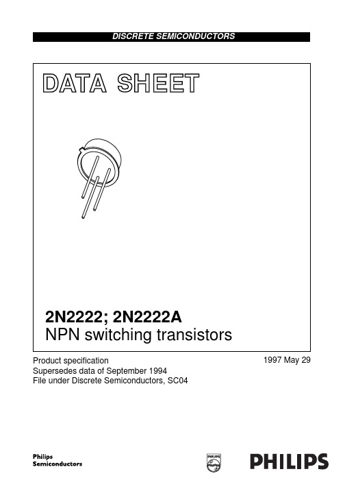
2N2222A中文资料_数据手册_参数
Objective specification Preliminary specification Product specification
This data sheet contains target or goal specifications for product development. This data sheet contains preliminary data; supplementary data may be published later. This data sheet contains final product specifications.
TO-18
1997 May 29
6
EUROPEAN PROJECTION
ISSUE DATE 97-04-18
Philips Semiconductors
NPN switching transistors
Product specification
2N2222; 2N2222A
DEFINITIONS
Data sheet status
SYMBOL
PARAMETER
Rth j-a Rth j-c
thermal resistance from junction to ambient thermal resistance from junction to case
CONDITIONS in free air
MIN.
MAX.
UNIT
−
60
Product specification
2N2222; 2N2222A
LIMITING VALUES In accordance with the Absolute Maximum Rating System (IEC 134).
CS42L52中文资料

Low Power, Stereo CODEC w/Headphone & Speaker AmpsStereo CODECHigh Performance Stereo ADC & DAC–98dB Dynamic Range (A-wtd) –-88dB THD+N Flexible Stereo Analog Input Architecture–4:1 Analog Input MUX –Analog Input Mixing–Analog Passthru with Volume Control–Analog Programmable Gain Amplifier (PGA) Programmable Automatic Level Control (ALC)–Noise Gate for Noise Suppression–Programmable Threshold & Attack/ReleaseRates Dual MIC Inputs–Differential or Single-Ended–+16dB to +32dB w/1dB step MIC Pre-Amplifiers–Programmable, Low Noise MIC Bias Levels Digital Signal Processing Engine–Bass & Treble Tone Control, De-Emphasis–Master Vol. and Independent PCM SDIN + ADC SDOUT Mix Volume Control–Soft-Ramp & Zero-Cross Transitions –Programmable Peak-Detect and Limiter –Beep Generator w/Full Tone ControlClass D Stereo/Mono Speaker AmplifierNo External Filter RequiredHigh Stereo Output Power at 10% THD+N– 2 x 1.00 W into 8Ω @ 5.0V – 2 x 550mW into 8Ω @ 3.7V – 2 x 230mW into 8Ω @ 2.5V High Mono Output Power at 10% THD+N– 1 x 1.90W into 4Ω @ 5.0V – 1 x 1.00W into 4Ω @ 3.7V – 1 x 350mW into 4Ω @ 2.5V Direct Battery Powered Operation–Battery Level Monitoring & Compensation 82% Efficiency at 800 mWPhase-Aligned PWM Output Reduces IdleChannel CurrentSpread Spectrum Modulation Low Quiescent CurrentStereo Headphone AmplifierGround Centered Outputs–No DC-Blocking Capacitors Required –Integrated Negative Voltage Regulator High Power Output at -75dB THD+N– 2 x 23mW Into 16Ω @ 1.8V – 2 x 44mW Into 16Ω @ 2.5V (Features continued on page 2)CS42L52CS42L52System Features12, 24, and 27MHz Master Clock Support inAddition to Typical Audio Clock Rates High Performance 24-bit Converters–Multi-bit Delta Sigma Architecture–Very Low 64Fs Oversampling Clock Reduces Power ConsumptionLow Power Operation–Stereo Analog Passthru: 10 mW @ 1.8 V –Stereo Playback: 14 mW @ 1.8 V–Stereo Rec. and Playback: 23 mW @ 1.8V Variable Power Supplies– 1.8 V to 2.5 V Digital & Analog – 1.6V to 5V Class D Amplifier– 1.8V to 2.5V Headphone Amplifier – 1.8 V to 3.3V Interface LogicPower Down Management–ADC, DAC, CODEC, MIC Pre-Amplifier, PGA,Headphone Amplifier, Speaker Amplifier Analog & Digital Routing/Mixes:–Line/Headphone Out =Analog In (ADCBypassed)–Line/Headphone/SpeakerOut =ADC +Digital In–Digital Out =ADC +Digital In –Internal Digital Loopback –Mono Mixes Flexible Clocking Options–Master or Slave Operation–High Impedance Digital Output Option (for easyMUXing between CODEC & other data sources)–Quarter-Speed Mode - (i.e. allows 8 kHz Fswhile maintaining a flat noise floor up to 16kHz)– 4 kHz to 96 kHz Sample Rates I²C ® Control Port OperationTemp. Monitor w/Thermal Foldback &ShutdownHeadphone/Speaker Detection Input Pop and Click SuppressionApplicationsDigital Voice Recorders, Digital Cameras &Camcorders PDA’sPersonal Media Players Portable Game ConsolesGeneral DescriptionThe CS42L52 is a highly integrated, low power stereo CODEC with headphone and Class D speaker amplifiers. The CS42L52 offers many features suitable for low power, porta-ble system applications.The ADC input path allows independent channel control of a number of features. Input summing amplifiers mix and select line-level and/or microphone level inputs for each channel.The microphone input path includes a selectable programma-ble-gain pre-amplifier stage and a low noise MIC bias voltage supply. A PGA is available for line or microphone inputs and provides analog gain with soft ramp and zero cross transi-tions. The ADC also features a digital volume control with soft ramp transitions. A programmable ALC and Noise Gate mon-itor the input signals and adjust the volume levels appropriately. To conserve power, the ADC may be bypassed while still allowing full analog volume control.The DAC output path includes a digital signal processing en-gine with various fixed function controls.Tone Control provides bass and treble adjustment of four selectable corner frequen-cies. The Digital Mixer provides independent volume control for both the ADC output and PCM input signal paths, as well as a master volume control. Digital Volume controls may be configured to change on soft ramp transitions while the analog controls can be configured to occur on every zero crossing.The DAC also includes de-emphasis, limiting functions and a BEEP generator delivering tones selectable across a range of two full octaves.The stereo headphone amplifier is powered from a separate positive supply and the integrated charge pump provides a negative supply. This allows a ground-centered analog output with a wide signal swing and eliminates external DC-blocking capacitors.The Class D stereo speaker amplifier does not require an external filter and provides the high efficiency amplification re-quired by power sensitive portable applications. The speaker amplifier may be powered directly from a battery while the in-ternal DC supply monitoring and compensation provides a constant gain level as the battery’s voltage decays. An internal temperature monitor alerts the user and automatically atten-uates and/or shuts down the PWM speaker output when an overload condition causes temperatures to exceed safe oper-ating levels.In addition to its many features, the CS42L52 operates from a low voltage analog and digital core making it ideal for portable systems that require extremely low power consumption in a minimal amount of space.The CS42L52 is available in a 40-pin QFN package in both Commercial (-40 to +85 °C) and Automotive (-40 to +105 °C)grades. The CS42L52 Customer Demonstration board is also available for device evaluation and implementation sugges-tions. Please refer to “Ordering Information” on page 82 for complete ordering information.CS42L52 TABLE OF CONTENTS1. PIN DESCRIPTIONS (8)1.1 I/O Pin Characteristics (9)2. TYPICAL CONNECTION DIAGRAM (10)3. CHARACTERISTIC AND SPECIFICATIONS (11)RECOMMENDED OPERATING CONDITIONS (11)ABSOLUTE MAXIMUM RATINGS (11)ANALOG INPUT CHARACTERISTICS (COMMERCIAL - CNZ) (12)ANALOG INPUT CHARACTERISTICS (AUTOMOTIVE - DNZ) (13)ADC DIGITAL FILTER CHARACTERISTICS (14)ANALOG OUTPUT CHARACTERISTICS (COMMERCIAL - CNZ) (15)ANALOG OUTPUT CHARACTERISTICS (AUTOMOTIVE - DNZ) (16)ANALOG PASSTHRU CHARACTERISTICS (17)PWM OUTPUT CHARACTERISTICS (Note 9) (17)LINE OUTPUT VOLTAGE LEVEL CHARACTERISTICS (18)HEADPHONE OUTPUT POWER CHARACTERISTICS (19)COMBINED DAC INTERPOLATION & ON-CHIP ANALOG FILTER RESPONSE (20)SWITCHING SPECIFICATIONS - SERIAL PORT (21)SWITCHING SPECIFICATIONS - I²C CONTROL PORT (22)DC ELECTRICAL CHARACTERISTICS (23)DIGITAL INTERFACE SPECIFICATIONS & CHARACTERISTICS (23)POWER CONSUMPTION (24)4. APPLICATIONS (25)4.1 Overview (25)4.1.1 Basic Architecture (25)4.1.2 Line & MIC Inputs (25)4.1.3 Line & Headphone Outputs (25)4.1.4 Speaker Driver Outputs (25)4.1.5 Fixed Function DSP Engine (25)4.1.6 Beep Generator (25)4.1.7 Power Management (25)4.2 Analog Inputs (26)4.2.1 MIC Inputs (27)4.2.2 Automatic Level Control (ALC) (27)4.2.3 Noise Gate (28)4.3 Analog Outputs (29)4.3.1 Beep Generator (30)4.3.2 Limiter (31)4.4 Analog In to Analog Out Passthru (32)4.4.1 Overriding the ADC Power Down (32)4.4.2 Overriding the PGA Power Down (33)4.5 PWM Outputs (33)4.5.1 Mono Speaker Output Configuration (33)4.5.2 VP Battery Compensation (33)4.5.2.1 Maintaining a Desired Output Level (34)4.6 Serial Port Clocking (34)4.7 Digital Interface Formats (36)4.7.1 DSP Mode (36)4.8 Initialization (36)4.9 Recommended Power-Up Sequence (37)4.10 Recommended Power-Down Sequence (37)4.11 Control Port Operation (38)4.11.1 I²C Control (38)CS42L524.11.2 Memory Address Pointer (MAP) (39)4.11.2.1 Map Increment (INCR) (39)5. REGISTER QUICK REFERENCE (40)6. REGISTER DESCRIPTION (42)6.1 Chip I.D. and Revision Register (Address 01h) (Read Only) (42)6.1.1 Chip I.D. (Read Only) (42)6.1.2 Chip Revision (Read Only) (42)6.2 Power Control 1 (Address 02h) (42)6.2.1 Power Down ADC Charge Pump (42)6.2.2 Power Down PGAx (42)6.2.3 Power Down ADCx (43)6.2.4 Power Down (43)6.3 Power Control 2 (Address 03h) (43)6.3.1 Power Down ADC Override (43)6.3.2 Power Down MICx (43)6.3.3 Power Down MIC Bias (43)6.4 Power Control 3 (Address 04h) (44)6.4.1 Headphone Power Control (44)6.4.2 Speaker Power Control (44)6.5 Clocking Control (Address 05h) (44)6.5.1 Auto-Detect (44)6.5.2 Speed Mode (45)6.5.3 32kHz Sample Rate Group (45)6.5.4 27 MHz Video Clock (45)6.5.5 Internal MCLK/LRCK Ratio (45)6.5.6 MCLK Divide By 2 (46)6.6 Interface Control 1 (Address 06h) (46)6.6.1 Master/Slave Mode (46)6.6.2 SCLK Polarity (46)6.6.3 ADC Interface Format (46)6.6.4 DSP Mode (46)6.6.5 DAC Interface Format (47)6.6.6 Audio Word Length (47)6.7 Interface Control 2 (Address 07h) (47)6.7.1 SCLK equals MCLK (47)6.7.2 SDOUT to SDIN Digital Loopback (47)6.7.3 Tri-State Serial Port Interface (48)6.7.4 Speaker/Headphone Switch Invert (48)6.7.5 MIC Bias Level (48)6.8 Input x Select: ADCA and PGAA (Address 08h), ADCB and PGAB (Address 09h) (48)6.8.1 ADC Input Select (48)6.8.2 PGA Input Mapping (49)6.9 Analog & HPF Control (Address 0Ah) (49)6.9.1 ADCx High-Pass Filter (49)6.9.2 ADCx High-Pass Filter Freeze (49)6.9.3 Ch. x Analog Soft Ramp (49)6.9.4 Ch. x Analog Zero Cross (49)6.10 ADC HPF Corner Frequency (Address 0Bh) (50)6.10.1 HPF x Corner Frequency (50)6.11 Misc. ADC Control (Address 0Ch) (50)6.11.1 ADC Channel B=A (50)6.11.2 Digital MUX (50)6.11.3 Digital Sum (50)6.11.4 Invert ADC Signal Polarity (50)CS42L526.11.5 ADC Mute (51)6.12 Playback Control 1 (Address 0Dh) (51)6.12.1 Headphone Analog Gain (51)6.12.2 Playback Volume Setting B=A (51)6.12.3 Invert PCM Signal Polarity (51)6.12.4 Master Playback Mute (51)6.13 Miscellaneous Controls (Address 0Eh) (52)6.13.1 Passthru Analog (52)6.13.2 Passthru Mute (52)6.13.3 Freeze Registers (52)6.13.4 HP/Speaker De-Emphasis (52)6.13.5 Digital Soft Ramp (53)6.13.6 Digital Zero Cross (53)6.14 Playback Control 2 (Address 0Fh) (53)6.14.1 Headphone Mute (53)6.14.2 Speaker Mute (53)6.14.3 Speaker Volume Setting B=A (54)6.14.4 Speaker Channel Swap (54)6.14.5 Speaker MONO Control (54)6.14.6 Speaker Mute 50/50 Control (54)6.15 MICx Amp Control:MIC A (Address 10h) & MIC B (Address 11h) (54)6.15.1 MIC x Select (54)6.15.2 MICx Configuration (55)6.15.3 MICx Gain (55)6.16 PGAx Vol. & ALCx Transition Ctl.:ALC, PGA A (Address 12h) & ALC, PGA B (Address 13h) (55)6.16.1 ALCx Soft Ramp Disable (55)6.16.2 ALCx Zero Cross Disable (55)6.16.3 PGAx Volume (56)6.17 Passthru x Volume: PASSAVOL (Address 14h) & PASSBVOL (Address 15h) (56)6.17.1 Passthru x Volume (56)6.18 ADCx Volume Control: ADCAVOL (Address 16h) & ADCBVOL (Address 17h) (57)6.18.1 ADCx Volume (57)6.19 ADCx Mixer Volume: ADCA (Address 18h) & ADCB (Address 19h) (58)6.19.1 ADC Mixer Channel x Mute (58)6.19.2 ADC Mixer Channel x Volume (58)6.20 PCMx Mixer Volume: PCMA (Address 1Ah) & PCMB (Address 1Bh) (58)6.20.1 PCM Mixer Channel x Mute (58)6.20.2 PCM Mixer Channel x Volume (58)6.21 Beep Frequency & On Time (Address 1Ch) (59)6.21.1 Beep Frequency (59)6.21.2 Beep On Time (60)6.22 Beep Volume & Off Time (Address 1Dh) (60)6.22.1 Beep Off Time (60)6.22.2 Beep Volume (61)6.23 Beep & Tone Configuration (Address 1Eh) (61)6.23.1 Beep Configuration (61)6.23.2 Beep Mix Disable (61)6.23.3 Treble Corner Frequency (62)6.23.4 Bass Corner Frequency (62)6.23.5 Tone Control Enable (62)6.24 Tone Control (Address 1Fh) (62)6.24.1 Treble Gain (62)CS42L526.24.2 Bass Gain (63)6.25 Master Volume Control: MSTA (Address 20h) & MSTB (Address 21h) (63)6.25.1 Master Volume Control (63)6.26 Headphone Volume Control: HPA (Address 22h) & HPB (Address 23h) (63)6.26.1 Headphone Volume Control (63)6.27 Speaker Volume Control: SPKA (Address 24h) & SPKB (Address 25h) (64)6.27.1 Speaker Volume Control (64)6.28 ADC & PCM Channel Mixer (Address 26h) (64)6.28.1 PCM Mix Channel Swap (64)6.28.2 ADC Mix Channel Swap (64)6.29 Limiter Control 1, Min/Max Thresholds (Address 27h) (65)6.29.1 Limiter Maximum Threshold (65)6.29.2 Limiter Cushion Threshold (65)6.29.3 Limiter Soft Ramp Disable (65)6.29.4 Limiter Zero Cross Disable (66)6.30 Limiter Control 2, Release Rate (Address 28h) (66)6.30.1 Peak Detect and Limiter (66)6.30.2 Peak Signal Limit All Channels (66)6.30.3 Limiter Release Rate (66)6.31 Limiter Attack Rate (Address 29h) (67)6.31.1 Limiter Attack Rate (67)6.32 ALC Enable & Attack Rate (Address 2Ah) (67)6.32.1 ALCx Enable (67)6.32.2 ALC Attack Rate (67)6.33 ALC Release Rate (Address 2Bh) (68)6.33.1 ALC Release Rate (68)6.34 ALC Threshold (Address 2Ch) (68)6.34.1 ALC Maximum Threshold (68)6.34.2 ALC Minimum Threshold (69)6.35 Noise Gate Control (Address 2Dh) (69)6.35.1 Noise Gate All Channels (69)6.35.2 Noise Gate Enable (69)6.35.3 Noise Gate Threshold and Boost (70)6.35.4 Noise Gate Delay Timing (70)6.36 Status (Address 2Eh) (Read Only) (70)6.36.1 Serial Port Clock Error (Read Only) (70)6.36.2 DSP Engine Overflow (Read Only) (71)6.36.3 PCMx Overflow (Read Only) (71)6.36.4 ADCx Overflow (Read Only) (71)6.37 Battery Compensation (Address 2Fh) (71)6.37.1 Battery Compensation (71)6.37.2 VP Monitor (71)6.37.3 VP Reference (72)6.38 VP Battery Level (Address 30h) (Read Only) (72)6.38.1 VP Voltage Level (Read Only) (72)6.39 Speaker Status (Address 31h) (Read Only) (72)6.39.1 Speaker Current Load Status (Read Only) (72)6.39.2 SPKR/HP Pin Status (Read Only) (73)6.39.3 Thermal Warning Status (Read Only) (73)6.39.4 Thermal Error Status (Read Only) (73)6.40 Temperature Monitor Control (Address 32h) (73)6.40.1 Temperature Acknowledge & Release (73)6.40.2 Thermal Foldback (Address 33h) (73)6.40.3 Thermal Foldback (73)CS42L526.40.4 Speaker Attenuation (74)6.41 Charge Pump Frequency (Address 34h) (74)6.41.1 Charge Pump Frequency (74)7. ANALOG PERFORMANCE PLOTS (75)7.1 Headphone THD+N versus Output Power Plots (75)8. EXAMPLE SYSTEM CLOCK FREQUENCIES (77)8.1 Auto Detect Enabled (77)8.2 Auto Detect Disabled (77)9. PCB LAYOUT CONSIDERATIONS (78)9.1 Power Supply, Grounding (78)9.2 QFN Thermal Pad (78)10. ADC & DAC DIGITAL FILTERS (79)11. PARAMETER DEFINITIONS (80)12. PACKAGE DIMENSIONS (81)THERMAL CHARACTERISTICS (81)13. ORDERING INFORMATION (82)14. REFERENCES (82)15. REVISION HISTORY (82)LIST OF FIGURESFigure 1. Typical Connection Diagram (10)Figure 2. Headphone Output Test Load (19)Figure 3. Serial Audio Interface Timing (21)Figure 4. Control Port Timing - I²C (22)Figure 5. Analog Input Signal Flow (26)Figure 6. Single-Ended MIC Configuration (27)Figure 7. Differential MIC Configuration (27)Figure 8. ALC (28)Figure 9. Noise Gate Attenuation (28)Figure 10. DSP Engine Signal Flow (29)Figure 11. PWM Output Stage (30)Figure 12. Analog Output Stage (30)Figure 13. Beep Configuration Options (31)Figure 14. Peak Detect & Limiter (32)Figure 15. Battery Compensation (34)Figure 16. I²S Format (36)Figure 17. Left-Justified Format (36)Figure 18. Right-Justified Format (DAC only) (36)Figure 19. DSP Mode Format) (36)Figure 20. Control Port Timing, I²C Write (38)Figure 21. Control Port Timing, I²C Read (38)Figure 22. THD+N vs. Output Power per Channel at 1.8V (16 Ω load) (75)Figure 23. THD+N vs. Output Power per Channel at 2.5V (16 Ω load) (75)Figure 24. THD+N vs. Output Power per Channel at 1.8V (32 Ω load) (76)Figure 25. THD+N vs. Output Power per Channel at 2.5V (32 Ω load) (76)Figure 26. ADC Passband Ripple (79)Figure 27. ADC Stopband Rejection (79)Figure 28. ADC Transition Band (79)Figure 29. ADC Transition Band Detail (79)Figure 30. DAC Passband Ripple (79)Figure 31. DAC Stopband (79)Figure 32. DAC Transition Band (79)Figure 33. DAC Transition Band (Detail) (79)CS42L52 1.PIN DESCRIPTIONSPin Name#Pin DescriptionSDA1Serial Control Data (Input/Output) - SDA is a data I/O in I²C Mode.SCL2Serial Control Port Clock (Input) - Serial clock for the serial control port.TSTN 3Test In - This pin is an input used for test purposes only. It must be tied to ground for normal oper-ation.SPKR_OUTA-SPKR_OUTB+ SPKR_OUTB-679PWM Speaker Output (Output) - Full-bridge amplified PWM speaker outputs.VP 58Power for PWM Drivers (Input)-Power supply for the PWM output driver stages.-VHPFILTpump that provides the negative rail for the headphone/line amplifiers.FLYN 11Charge Pump Cap Negative Node (Output)- Negative node for the inverting charge pump’s fly-ing capacitor.FLYPcapacitor.+VHP13Positive Analog Power for Headphone (Input)-Positive voltage rail and power for the internal headphone amplifiers and inverting charge pump.SDOUTMCLKSCLKSDINSDALRCKFLYN+VHPHP/LINE_OUTBHP/LINE_OUTAVQMICBIASAIN4A/MIC1+/MIC2AAIN2ATSTNSPKR_OUTA+VPVPVDSPKR_OUTB--VHPFILTAIN4B/MIC2+/MIC2BAIN1BAIN2BAFILTBAIN3B/MIC2-/MIC1BAFILTAAIN1AAIN3A/MIC1-/MIC1ASPKR_OUTB+SCLDGNDSPKR_OUTA-FLYPVAAGNDFILT+RESETVLSPKR/HPCS42L521.1I/O Pin CharacteristicsInput and output levels and associated power supply voltage are shown in the table below. Logic levels should not exceed the corresponding power supply voltage.FILT+cuits.VQ 19Quiescent Voltage (Output ) - Filter connection for the internal quiescent voltage.MICBIAS 20Microphone Bias (Output ) - Low noise bias supply for an external microphone. Electrical charac-teristics are specified in the DC Electrical Characteristics table.AIN3A,B 23,24Line-Level Analog Inputs (Input ) - Single-ended stereo line-level analog inputs. MIC1+,-MIC2+,-21,2322,24Differential Microphone Inputs (Input ) - Differential stereo microphone inputs. MIC1A,B 23,24Single-Ended Microphone Inputs (Input ) - Single-ended stereo microphone inputs.AIN2A,B AIN1A,B 25,2629,30Line-Level Analog Inputs (Input ) - Single-ended stereo line-level analog inputs.SPKR/HP and/or headphone outputs.RESET 32Reset (Input ) - The device enters a low power mode when this pin is driven low.VL face and host control port.VD 34Digital Power (Input ) - Positive power for the internal digital section. DGND 35Digital Ground (Input ) - Ground reference for the internal digital section.SDOUT 36Serial Audio Data Output (Output ) - Output for two’s complement serial audio data.MCLK 37Master Clock (Input ) - Clock source for the delta-sigma modulators.SCLK 38Serial Clock (Input/Output ) - Serial clock for the serial audio interface.SDIN 39Serial Audio Data Input (Input ) - Input for two’s complement serial audio data.LRCK40Left Right Clock (Input/Output ) - Determines which channel, Left or Right, is currently active on the serial audio data line.GND/Thermal Paddissipation.Power SupplyPin Name I/O DriverReceiverVLRESET Input - 1.65 V - 3.47 V, with Hysteresis SCL Input - 1.65 V - 3.47 V, with Hysteresis SDA Input/Output 1.65 V - 3.47 V, CMOS/Open Drain1.65 V - 3.47 V, with HysteresisMCLK Input - 1.65 V - 3.47 V LRCK Input/Output 1.65 V - 3.47 V, CMOS 1.65 V - 3.47 V SCLK Input/Output 1.65 V - 3.47 V, CMOS 1.65 V - 3.47 VSDOUT Output 1.65 V - 3.47 V V, CMOSSDIN Input - 1.65 V - 3.47 V VA SPKR/HP Input - 1.65 V - 2.63 VVPSPKR_OUTA+Output 1.6V - 5.25V Power MOSFET -SPKR_OUTA-Output1.6V - 5.25V Power MOSFET -SPKR_OUTB+Output 1.6V - 5.25V Power MOSFET -SPKR_OUTB-Output1.6V - 5.25V Power MOSFET-CS42L52 2.TYPICAL CONNECTION DIAGRAMFigure 1. Typical Connection DiagramCS42L523.CHARACTERISTIC AND SPECIFICATIONS RECOMMENDED OPERATING CONDITIONS(AGND=DGND=0 V, all voltages with respect to ground.)ABSOLUTE MAXIMUM RATINGS(AGND = DGND = 0 V; all voltages with respect to ground.)WARNING:Operation at or beyond these limits may result in permanent damage to the device. Normal operationis not guaranteed at these extremes.Notes:1.Any pin except supplies. Transient currents of up to ±100 mA on the analog input pins will not causeSCR latch-up.2.The maximum over/under voltage is limited by the input current.ParametersSymbol Min MaxUnitsDC Power Supply AnalogVA 1.65 2.63V Headphone Amplifier +VHP 1.65 2.63V Speaker Amplifier VP 1.60 5.25V DigitalVD 1.65 2.63V Serial/Control Port Interface VL1.65 3.47V Ambient TemperatureCommercial - CNZ Automotive - DNZT A-40-40+85+105°C °CParametersSymbolMinMaxUnitsDC Power SupplyAnalog Speaker DigitalSerial/Control Port InterfaceVA, VHP VP VD VL -0.3-0.3-0.3-0.3 3.05.53.04.0V V V V Input Current(Note 1)I in-±10mAAnalog Input Voltage(Note 2)V INAGND-0.7VA+0.7VDigital Input Voltage(Note 2)V IND -0.3VL+ 0.4V Ambient Operating Temperature (power applied)T A -50+115°C Storage TemperatureT stg-65+150°CCS42L52ANALOG INPUT CHARACTERISTICS (COMMERCIAL - CNZ)(Test Conditions (unless otherwise specified): Input sine wave (relative to digital full-scale): 1kHz through passive input filter; VL = VD = VHP = 1.8 V; T A = +25°C; Measurement Bandwidth is 10Hz to 20kHz unless otherwise specified. Sample Fre-quency = 48kHz)3.Measured with DAC delivering full-scale output into specified load.4.Measured between analog input and AGND.VA = 2.5V VA = 1.8V Parameters MinTypMaxMinTypMaxUnitAnalog In to ADC (PGA bypassed)Dynamic RangeA-weighted unweighted 93909996--90879693--dB dB Total Harmonic Distortion + Noise-1dBFS -20dBFS -60dBFS ----86-76-36-80--30----84-73-33-78--27dB dB dB Analog In to PGA to ADC Dynamic Range PGA Setting: 0 dB A-weighted unweighted 92899895--89869592--dB dB PGA Setting: +12 dBA-weighted unweighted85829188--82798885--dB dB Total Harmonic Distortion + Noise PGA Setting: 0 dB -1dBFS -60dBFS ---88-35-82-29---86-32-80-26dB dB PGA Setting: +12 dB -1dBFS --85-79--83-77dB Analog In to MIC Pre-Amp (+16 dB) to PGA to ADC Dynamic Range PGA Setting: 0 dB A-weighted unweighted --8683----8380--dB dB Total Harmonic Distortion + Noise PGA Setting: 0 dB -1dBFS --76---74-dB Analog In to MIC Pre-Amp (+32 dB) to PGA to ADC Dynamic Range PGA Setting: 0 dB A-weighted unweighted --7874----7571--dB dB Total Harmonic Distortion + Noise PGA Setting: 0 dB -2dBFS --74---71-dB Other Characteristics DC AccuracyInterchannel Gain Mismatch -0.2--0.2-dB Gain Drift -±100--±100-ppm/°C Offset Error SDOUT Code with HPF On -352--352-LSB InputInterchannel Isolation -90--90-dB HP Amp to Analog Input Isolation R L = 10 k Ω(Note 3)R L = 16 Ω--10070----10070--dB dB Speaker Amp to Analog Input Isolation -60--60-dB Full-scale Input Voltage ADC PGA (0 dB)PGA (+12 dB)MIC (+16 dB)MIC (+32 dB)0.73•VA0.73•VA 0.769•VA 0.770•VA 0.194•VA 0.115•VA 0.019•VA0.83•VA0.83•VA 0.73•VA 0.73•VA0.769•VA 0.770•VA 0.194•VA 0.115•VA 0.019•VA 0.83•VA 0.83•VAVpp Vpp Vpp Vpp Input Impedance (Note 4)ADC PGA MIC ---203950------203950---k Ωk Ωk ΩCS42L52 ANALOG INPUT CHARACTERISTICS (AUTOMOTIVE - DNZ)(Test Conditions (unless otherwise specified): Input sine wave (relative to full-scale): 1 kHz through passive input filter;VL = VD = VHP = 1.8 V; T A = -40 to +85°C; Measurement Bandwidth is 10Hz to 20kHz unless otherwise specified. Sample Frequency = 48kHz)VA = 2.37 - 2.63 V VA = 1.65 - 1.89 VParameters Min Typ Max Min Typ Max Unit Analog In to ADCDynamic Range A-weightedunweighted 91889996--88859693--dBdBTotal Harmonic Distortion + Noise -1dBFS -20dBFS-60dBFS ----86-76-36-78--28----84-73-33-76--25dBdBdBAnalog In to PGA to ADC Dynamic RangePGA Setting: 0 dB A-weightedunweighted 90879895--87849592--dBdBPGA Setting: +12 dB A-weightedunweighted 83809188--80778885--dBdBTotal Harmonic Distortion + NoisePGA Setting: 0 dB -1dBFS -60dBFS ---88-35-80-27---86-32-78-24dBdBPGA Setting: +12 dB -1dBFS--85-77--83-75dB Analog In to MIC Pre-Amp (+16 dB) to PGA to ADCDynamic RangePGA Setting: 0 dB A-weightedunweighted --8683----8380--dBdBTotal Harmonic Distortion + NoisePGA Setting: 0 dB -1dBFS--76---74-dB Analog In to MIC Pre-Amp (+32 dB) to PGA to ADCDynamic RangePGA Setting: 0 dB A-weightedunweighted --7874----7571--dBdBTotal Harmonic Distortion + NoisePGA Setting: 0 dB -2dBFS--74---71-dB Other CharacteristicsDC AccuracyInterchannel Gain Mismatch-0.1--0.1-dB Gain Drift-±100--±100-ppm/°C Offset Error SDOUT Code with HPF On-352--352-LSB InputInterchannel Isolation-90--90-dBHP Amp to Analog Input Isolation R L = 10 kΩ(Note 3)R L = 16 Ω--10070----10070--dBdBSpeaker Amp to Analog Input Isolation-60--60-dBFull-scale Input Voltage ADCPGA (0 dB)PGA (+12 dB)MIC (+16 dB)MIC (+32 dB)0.73•VA0.73•VA0.769•VA0.770•VA0.194•VA0.115•VA0.019•VA0.83•VA0.83•VA0.73•VA0.73•VA0.769•VA0.770•VA0.194•VA0.115•VA0.019•VA0.83•VA0.83•VAVppVppVppVppInput Impedance (Note 4)ADCPGAMIC 184050------184050------kΩkΩkΩCS42L52ADC DIGITAL FILTER CHARACTERISTICS5.Response is clock-dependent and will scale with Fs. Note that the response plots (Figures 26to 29 onpage 79) have been normalized to Fs and can be de-normalized by multiplying the X-axis scale by Fs.HPF parameters are for Fs = 48 kHz.Parameters (Note 5)MinTypMaxUnitPassband (Frequency Response) to -0.1 dB corner0-0.4948Fs Passband Ripple -0.09-0.17dB Stopband0.6--Fs Stopband Attenuation 33--dB Total Group Delay-7.6/Fs -s High-Pass Filter Characteristics (48 kHz Fs)Frequency Response -3.0 dB -0.13 dB-- 3.624.2--Hz Hz Phase Deviation @ 20Hz-10-Deg Passband Ripple --0.17dB Filter Settling Time-105/Fss。
2N7002中文资料(fairchild)中文数据手册「EasyDatasheet - 矽搜」

1995年11月
2N7000 / 2N7002 / NDS7002A N沟道增强型场效应晶体管
概述
这些N沟道增强型场效应晶体管 采用飞兆半导体专有,高密度生产, DMOS技术.这些产品目是为最大限度地减少通态电阻 ,同时提供坚固,可靠和快速开关性能.他们可以在需要高 达400mA DC大多数应用中使用,并且可以提供脉冲电流 高达2A.这些产品特别适用于低电压,低电流应用, 如小伺服电机控制,功率MOSFET栅极驱动器,和其他开关 应用.
V 1 µA 1 mA 1 µA 0.5 mA 10 nA 100 nA
-10 nA -100 nA
V = V , I =1毫安
2N7000 0.8 2.1 3
V
V = V , I = 250 µA
2N7002 1 2.1 2.5 NDS7002A
= 10 V, I =500毫安
2N7000
1.2 5
T =125°C
1.9 9
V = 4.5 V, I =75毫安
1.8 5.3
V = 10 V, I =500毫安
2N7002
1.2 7.5
T =100°C
1.7 13.5
V = 5.0 V, I =50毫安
1.7 7.5
T =100C
2.4 13.5
V = 10 V, I =500毫安
NDS7002 A
V在
VGS
R GEN
G
V DD
RL
D
V出
DUT
S
图 11.
t d(on)
t on tr
90%
t d(of f )
t of f tf
材料2A12
资料2A12-T4之阿布丰王创作2A12-T4为铝-铜-镁系中的典范硬铝合金,其成分比力合理,综合性能较好.很多国家都生产这个合金,是硬铝中用量最年夜的.该合金的特点是:强度高,有一定的耐热性,可用作150°C以下的工作零件.温度高于125°C,2A12-T4合金的强度比7075合金的还高.热状态、退火和新淬火状态下成形性能都比力好,热处置强化效果显著,但热处置工艺要求严格.抗蚀性较差,但用纯铝包覆可以获得有效呵护;焊接时易发生裂纹,但采纳特殊工艺可以焊接,也可以铆接.广泛用于飞机结构、铆钉、卡车轮毂、螺旋桨元件及其他种种结构件.2A12-T4合金的化学成分(以最高百分比暗示,除非列出的是一个范围值)2A12合金的机械及物理性能抗拉强度MPa4700.2%屈服强度MPa325伸长率%10疲劳强度105硬度HB120电导率20°C3020°C电阻率n.m 48弹性模量68密度2A12铝合金:2A12铝合金为一种高强度硬铝,可进行热处置强化,在退火、刚淬火和热状态下可塑性中等,2A12铝合鑫点焊焊接性良好,用气焊和氩弧焊时有形成晶间裂纹的倾向;,2A12铝合金在淬火和冷作硬化后可切削性能尚好,在退火状态时不良.抗蚀性不高,常采纳阳极氧化处置与涂漆方法或概况加包铝层以提高抗腐蚀能力.2A12铝合金热处置规范:1) 均匀化退火:加热480~495℃;保温12~14h;炉冷.2)完全退火:加热390~430℃;保温时间30~120min;炉冷至300℃,空冷. 3)快速退火:加热350~370℃;保温时间为30~120min;空冷.4)淬火和时效:淬火495~505℃,水冷;人工时效 185~195℃,6~12h,空冷;自然时效:室温96h.。
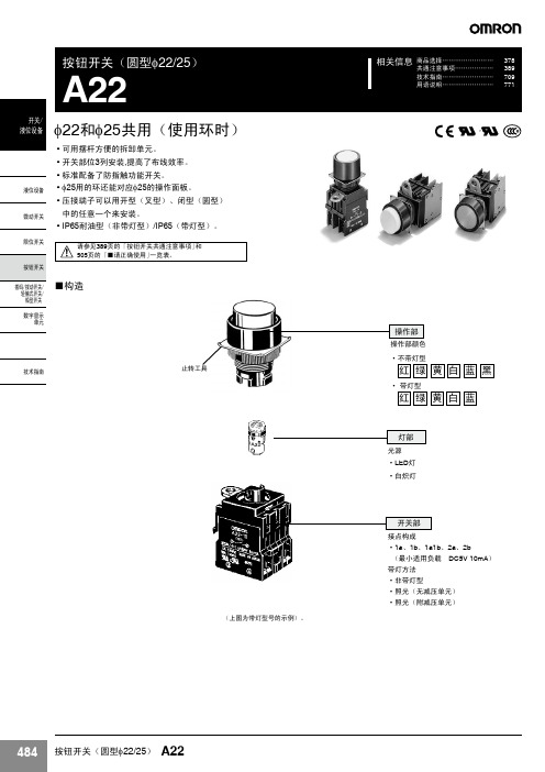
A22
交替动作(自我保持型) 成套型号
A22L-T□-6D-10A A22L-T□-6A-10A A22L-T□-12A-10A A22L-T□-24A-10A A22L-T□-6D-01A A22L-T□-6A-01A A22L-T□-12A-01A A22L-T□-24A-01A A22L-T□-6D-11A A22L-T□-6A-11A A22L-T□-12A-11A A22L-T□-24A-11A A22L-T□-6D-20A A22L-T□-6A-20A A22L-T□-12A-20A A22L-T□-24A-20A A22L-T□-6D-02A A22L-T□-6A-02A A22L-T□-12A-02A A22L-T□-24A-02A A22L-T□-T1-10A A22L-T□-T2-10A A22L-T□-T1-01A A22L-T□-T2-01A A22L-T□-T1-11A A22L-T□-T2-11A A22L-T□-T1-20A A22L-T□-T2-20A A22L-T□-T1-02A A22L-T□-T2-02A
按钮开关(圆型f22/25)
A22
ᓔ݇
⎆ԡ䆒 f22和f25共用(使用环时)
⎆ԡ䆒 ᖂࡼᓔ݇
• 可用摆杆方便的拆卸单元。 • 开关部位3列安装,提高了布线效率。 • 标准配备了防指触功能开关。 • f25用的环还能对应f25的操作面板。 • 压接端子可以用开型(叉型)、闭型(圆型)
中的任意一个来安装。 • IP65耐油型(非带灯型)/IP65(带灯型)。
□操作部颜色 符号(颜色)
R(红) Y(黄) G(绿) W(白) A(蓝) B(黑)
请参照490~492页…单品订购型号 (操作部·灯部·开关部可以按各别型号订购)。
2N2218A中文资料

2N2218A中文资料Meets MIL 19500 /251Collector - Base Voltage 75V ? Collector - Current 800 mAMedium Current, Bipolar TransistorMaximum RatingsRATINGSYMBOL VALUE UNIT Collector - Emitter Voltage V CEO 50Vdc Collector - Base Voltage V CBO 75Vdc Emitter - Base VoltageV EBO6Vdc Collector Current - ContinuousI C800mAdc Total Device Dissipation @ T A = 25 °C P D 0.8WATTS Derate above 25 °C4.6mW/°C Total Device Dissipation @ T C =25 °C P D 3.0WATTS Derate above 25 °C17.0mW/°C Operating Junction&Storage Temperature RangeT J , T stg- 55 to +200°CThermal CharacteristicsCHARACTERISTICSYMBOL MAX UNIT Thermal Resistance, Junction to Ambient R θ JA 217°C/W Thermal Resistance, Junction to Case R θ JC59°C/WSWITCHING TRANSISTOR JAN, JANTX, JANTXVElectrical Characteristics (T A = 25°C unless otherwise noted) OFF CHARACTERISTIC SYMBOL MIN MAX UNIT Collector - Emitter Breakdown Voltage (1)V(BR)CEO( I C = 10 mA dc, I B = 0 )50Vdc Collector - Base Breakdown Voltage V(BR)CBO( I C = 10 μAdc, I E = 0 )75Vdc Emitter - Base Breakdown Voltage V(BR)EBO( I E = 10 μAdc, I C = 0 ) 6Vdc Collector - Emitter Cutoff Current I CES( V CE = 50 Vdc )10nAdc Collector - Base Cutoff Current I CBO ( V CB = 60 Vdc, I E = 0 )10nAdc ( V CB = 60 Vdc, I E = 0, T A = 150 °C )10μAdc Emitter - Base Cutoff Current I EBO ( V EB = 4 Vdc )10nAdc ( V EB = 6 Vdc )10μAdc ON CHARACTERISTIC SYMBOL MIN MAX UNIT DC Current Gain h FE ( I C = 0.1 mA dc, V CE = 10 Vdc ) (1)30( I C = 1 mA dc, V CE = 10 Vdc ) (1)35150( I C = 10 mA dc, V CE = 10 Vdc ) (1)40( I C = 150 mA dc, V CE = 10 Vdc ) (1)40120( I C = 500 mA dc, V CE = 10 Vdc ) (1)20( I C = 10 mA dc, V CE = 10 Vdc, T J =-55°C) (1)35Collector - Emitter Saturation Voltage V CE(sat)( I C = 150 mAdc, I B = 15 mAdc ) (1)0.3Vdc ( I C = 500 mAdc, I B = 50 mAdc ) (1) 1.0Vdc Base - Emitter Saturation Voltage V BE(sat)( I C = 150 mAdc, I B = 15 mAdc ) (1)0.6 1.2Vdc ( I C = 500 mAdc, I B = 50 mAdc ) (1) 2.0Vdc 1. Pulse Tes t: Pulse Width ≤ 300 μs, Duty Cycle ≤.2%Electrical Characteristics (T A = 25°C unless otherwise noted) SMALL - SIGNAL CHARACTERISTICS SYMBOL MIN MAX UNIT Output Capacitance C obo( V CB = 10 Vdc, I E = 0, 100kHz ≤ f ≤ 1 MHz )8.0pF Input Capacitance C ibo( V EB = 0.5 Vdc, I C = 0, 100kHz ≤ f ≤ 1 MHz )25pF SWITCHING CHARACTERISTICS SYMBOL MIN MAX UNIT Turn -On Time t on( V CC = 30 Vdc, I C = 150 mAdc,I B1 =15 mAdc) ( See FIGURE 1 )35ns Turn - Off Time t off( V CC = 30 Vdc, I C = 150 mAdc,I B1 = - I B2 = 15 mAdc) ( See FIGURE 2 )300ns Small - Signal AC Characteristics (T A = 25°C)LOW FREQUENCY SYMBOL MIN MAX UNIT Common - Emitter Forward Current Transfer Ratio h fe( I C = 1 mA, V CE = 10 V, f = 1kHz )35HIGH FREQUENCYCommon - Emitter Forward Current Transfer Ratio|h fe|( I C = 20 mA, V CE = 20 V, f = 100 MHz ) 2.512S p i c e M o d e l (based upon typical device characteristics) *1Q2N2218A NPN ( IS = 21.2f XTI = 3.0 EG = 1.11 VAF= 103.8 BF = 90.7 ISE = 3.34p + NE = 2.05 IKF = 1.255 NK = 0.9394 XTB = 1.5 BR = 1.031 ISC = 3.299p + NC = 1.605 IKR =0.8992 RC = 0.0 CJC = 19.4p MJC = 0.3333 VJC = 0.75 + FC = 0.5 CJE=29.6p MJE= 0.3333 VJE = 0.75 TR = 275.0n TF=564.5p + ITF = 1.0 XTF= 0.0 VTF=10.0 )*1. Microsemi Corp. claims no responsibility for misapplication of Spice Model information. Spice modeling should be used as a precursor guide to in-circuit performance. Actual performance is the responsibility of the user/designer.TO-39 CASE OUTLINEDIE OUTLINEFIGURE 1 Saturated Turn-on Time Test CircuitFIGURE 2 Saturated Turn-off Time Test CircuitFIGURE 3FIGURE 4.0001.001.01.11IC COLLECTOR CURRENT (A)255075100125h F E C U R R E N T G A I N255075100125DC CURRENT GAINVCE = 10 Vtyp @ 25Ctyp @ -55C.0001.001.01IB, BASE CURRENT (A)0.00.20.40.60.81.0V C E , C O L L E C T O R -E M I T T E R (V ) 0.00.20.40.60.81.0COLLECTOR SATURATION vs BASE CURRENT TJ = 25 CIC = 500 mAIC = 150 mAFIGURE 5FIGURE 6.001.01.11IB, BASE CURRENT (A)0.500.751.001.25V B E , B A S E -E M I T T E R V O L T A G E (V )0.751.001.25BASE SATURATION vs BASE CURRENTTJ = 25 CIC = 150 maIC = 500 ma.01.1110100REVERSE JUNCTION VOLTAGE (V)51015202530J U N C T I O N C A P A C I T A N C E (p F )051015202530JUNCTION CAPACITANCE TJ = 25 C 100 kHz < f < 1 MHz COBOCIBOFIGURE 7FIGURE 810100COLLECTOR CURRENT (mA) 10100t o n T I M E (n s )10100SWITCHING TURN - 0N TIME TJ = 25 C IC/IB = 10min.max.50010100COLLECTOR CURRENT (mA) 1001000t o f f T I M E (n s ) 1001000SWITCHING TURN - OFF TIME TJ = 25 C IC/IB = 10min.max.FIGURE 91101001000FREQUENCY MHz.01.11N O R M A L I Z E D G A I N.01.11NORMALIZED GAIN VS FREQUENCY TJ = 25C IC = 20 mA VCE = 20 V。
阿尔法电缆 Alpha Wire 型号2422C的产品说明书
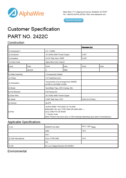
Alpha Wire | 711 Lidgerwood Avenue, Elizabeth, NJ 07207Tel: 1-800-52 ALPHA (25742), Web: Customer Specification PART NO. 2422CConstructionDiameters (In)1) Component 1 2 X 1 CONDa) Conductor 18 (16/30) AWG Tinned Copper 0.047 b) Insulation 0.016" Wall, Nom. FRPE 0.079(1) Color Code Alpha Wire Color Code D Cond Color Cond Color CondColor1BLACK2RED2) Cable Assembly 2 Components Cabled a) Twists: 5.3 Twists/foot (min)b) Orientation: Components to be arranged from INSIDE LAYER to OUTSIDE LAYER 3) Shield: Alum/Mylar Tape, 25% Overlap, Min.a) Foil Direction Foil Facing Outb) Drain Wire 20 (10/30) AWG Tinned Copper 4) Jacket 0.020" Wall, Nom.,PVC 0.202 (0.212 Max.)a) Color(s)SLATEb) PrintALPHA WIRE-* P/N 2422C 2C 18 AWGSHIELDED 75C (UL) TYPE CMG OR AWM 2092 ----C(UL) CMG FT4 CE ROHS * = Factory Code[Note: Product may have c(UL) or CSA markings depending upon plant of manufacture.]Applicable Specifications1) ULAWM/STYLE 2092 60°C / 300 V RMS CMG 75°CVW-12) CSA InternationalC(UL) TYPE CMG 75°CFT43) CE:EU Low Voltage Directive 2014/35/EUEnvironmental1) CE: EU Directive 2011/65/EU(RoHS2), EU Directive 2015/863/EU (RoHS3):This product complies with European Directive 2011/65/EU (RoHS Directive) of the EuropeanParliament and of the Council of 8 June 2011 and the amending Directive 2015/863/EU of 4June 2015 . No Exemptions are required for RoHS Compliance on this item. Consult AlphaWire's web site for RoHS C of C.2) California Proposition 65:Exempt from warning labels based on the Consent Judgment. Please see Alpha's CA Prop 65 Statement for more information.PropertiesPhysical & Mechanical Properties1) Temperature Range-20 to 75°C2) Bend Radius 10X Cable Diameter3) Pull Tension 33 Lbs, MaximumElectrical Properties(For Engineering purposes only)1) Voltage Rating 300 V RMS2) Capacitance 31 pF/ft @1 kHz, Nominal Conductor to Conductor3) Ground Capacitance56 pF/ft @1 kHz, Nominal4) Characteristic Impedance54 Ω5) Inductance0.18 µH/ft, Nominal6) Conductor DCR7 Ω/1000ft @20°C, Nominal7) OA Shield DCR8.5 Ω/1000ft @20°C, NominalOtherPackaging Flange x Traverse x Barrel (inches)a) 1000 FT12 x 10 x 5 Continuous lengthb) BOX 1000FT11-3/4 EASY REEL: Continuous lengthc) BOX 500FT9-1/2 EASY REEL: Continuous lengthd) 500 FT12 x 4.5 x 3.5 Continuous lengthe) 100 FT 6.5 x 4 x 2.5 Continuous length[Spool dimensions may vary slightly]Alpha Wire | 711 Lidgerwood Avenue, Elizabeth, NJ 07207Tel: 1-800-52 ALPHA (25742)Although Alpha Wire (“Alpha”) makes every reasonable effort to ensure their accuracy at the time of publication, information and specifications described herein are subject to errors or omissions and to changes without notice, and the listing of such information and specifications does not ensure product availability.Alpha provides the information and specifications herein on an “AS IS” basis, with no representations or warranties, whether express, statutory or implied. In no event will Alpha be liable for any damages (including consequential, indirect, incidental, special, punitive, or exemplary) whatsoever, even if Alpha had been advised of the possibility of such damages, whether in an action under contract, negligence or any other theory, arising out of or in connection with the use, or inability to use, the information or specifications described herein.ALPHA WIRE - CONFIDENTIAL AND PROPRIETARYNotice to persons receiving this document and/or technical information. This document is confidential and is the exclusive property of ALPHA WIRE, and is merely on loan and subject to recall by ALPHA WIRE at any time. By taking possession of this document, the recipient acknowledges and agrees that this document cannot be used in any manner adverse to the interests of ALPHA WIRE, and that no portion of this document may be copied or otherwise reproduced without the prior written consent of ALPHA WIRE. In the case of conflicting contractual provisions, this notice shall govern the status of this document. ©2013 ALPHA WIRE - all rights reserved.EU/China ROHS CERTIFICATE OF COMPLIANCETo Whom It May Concern:Alpha Wire Part Number: 2422C2422C , RoHS-Compliant Commencing With 8/1/2005 ProductionNote: all colors and put-upsThis document certifies that the Alpha part number cited above is manufactured in accordance with Directive 2011/65/EU of the European Parliament, better known as the RoHS Directive (commonly known as RoHS 2), with regards to restrictions of the use of certain hazardous substances used in the manufacture of electrical and electronic equipment. This certification extends to amending Directive 2015/863/EU which expanded the list of restricted substances to 10 items (commonly known as RoHS 3) The reader is referred to these Directives for the specific definitions and extents of the Directives. No Exemptions are required for RoHS Compliance on this item. Additionally, Alpha certifies that the listed part number is in compliance with China RoHS “Marking for Control of Pollution by Electronic Information Products” standard SJ/T 11364-2014. Substance Maximum Control ValueLead0.1% by weight (1000 ppm)Mercury0.1% by weight (1000 ppm)Cadmium0.01% by weight (100 ppm)Hexavalent Chromium0.1% by weight (1000 ppm )Polybrominated Biphenyls (PBB)0.1% by weight (1000 ppm)Polybrominated Diphenyl Ethers (PBDE) ,Including Deca-BDE0.1% by weight (1000 ppm)Bis(2-ethylhexyl) phthalate (DEHP)0.1% by weight (1000 ppm)Butyl benzyl phthalate (BBP)0.1% by weight (1000 ppm)Dibutyl phthalate (DBP) 0.1% by weight (1000 ppm)Diisobutyl phthalate (DIBP)0.1% by weight (1000 ppm)The information provided in this document and disclosure is correct to the best of Alpha Wire's knowledge, information and belief at the date of its release. The information provided is designed only as a general guide for the safe handling, storage, and any other operation of the product itself or the one that it will become part of. The intent of this document is not to be considered a warranty or quality specification. Regulatory information is for guidance purposes only. Product users are responsible for determining the applicability of legislation and regulations based on their individual usage of the product.Authorized Signatory for the Alpha Wire:Dave Watson, Director of Engineering & QA8/27/2019Alpha Wire711 Lidgerwood Ave.Elizabeth, NJ 07207Tel: 1-908-925-8000。
A2级别铝复合板产品资料书
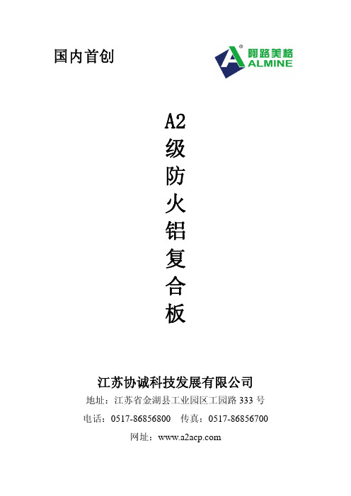
A2 级 防 火 铝 复 合 板
江苏协诚科技发展有限公司
地址:江苏省金湖县工业园区工园路 333 号 电话:0517-86856800 传真:0517-86856700
网址:
引言
我公司生产的 A2 级防火铝复合板是一种新型的不燃装饰材料,利用不燃无机物 作为芯材,表面为 PVDF 涂层铝合金。通过先进的工艺使其达到完美的结合。从 而形成一种外观时尚、性能优越、施工方便的新一代室内外装饰材料。
澳大利亚— 市府大楼外立面、吊顶
工程
72
国内首创 A2级防火铝复合板
海外工程
澳大利亚一凯恩斯植物公园 镜面不锈钢A2复合板工程
73
国内首创 A2级防火铝复合板
海外工程
74
国内首创 A2级防火铝复合板
海外工程
75
国内首创 A2级防火铝复合板
海外工程
76
国内首创 A2级防火铝复合板
海外工程
19
5) 涂层光泽度偏差:≤10 6) 表面铅笔硬度:≥1H 7) 涂层柔韧性: ≤2T 8) 涂层附着力:不次于1级 9) 耐冲击性:≥20kg.cm 不脱漆,无裂痕 10) 涂层耐热水性:无异常 11) 涂层耐沾污性:≤5% 12) 涂层耐酸性:无变化 13) 涂层耐碱性:无变化 14) 涂层耐油性:无变化 15) 涂层耐溶剂性:不露底 16) 剥离强度(按180°测试方式): 平均值≥5.0N/mm 最小值≥3.0N/mm 17) 热变形温度:≥95℃ 18) 耐温差性: 剥离强度下降率: ≤10% 附着力:不次于1级 外观:无变化 19)燃烧性能等级:
公司营业执照 ........................................ 1-2 2.企业荣誉
- 1、下载文档前请自行甄别文档内容的完整性,平台不提供额外的编辑、内容补充、找答案等附加服务。
- 2、"仅部分预览"的文档,不可在线预览部分如存在完整性等问题,可反馈申请退款(可完整预览的文档不适用该条件!)。
- 3、如文档侵犯您的权益,请联系客服反馈,我们会尽快为您处理(人工客服工作时间:9:00-18:30)。
CONTACT RESISTANCE: Below 20 m Ω typ. initial @ 2-4 V DC, 100 mA, for both silver and gold plated contacts.
Switchlock
Switch and lock Function
A21613 DP, 30°, keypull pos. 1
A11413 SP, 90°, keypull pos. 1 A31413 3P, 90º, keypull pos. 1 A3141U 3P, 90°, keypull pos. 1 & 2
A 4 Tumbler lock
A11613 SP, 30°, keypull p05. 1
G 5 Tumbler lock with anti-static switch
A1161U SP, 30°, keypull pos. 1 & 4 Y 4 Tumbler lock with anti-static switch
NOTE: Specifications and materials listed above are for switchlocks with standard options. For information on specific and custom switchlocks, consult Customer Service Center.
CONNECTED TERMINALS
POS. 2
POS. 3
A-4 A-4, B-8, C-12
3P
A3141U A-1, B-5, C-9
A-2
A-4
3P
A31513 A-1, B-5, C-9
A-2, B-6, C-10
A-4, B-8, C-12
Build-A-Switch
To order, simply select desired option from each category and place in the appropriate box. Available options are shown and described on pages M–35 through M–38. For additional options not shown in catalog, consult Customer Service Center.
Contact Material Q Silver B Gold
Seal NONE No seal E Epoxy seal
M–34
Dimensions are shown: Inch (mm) Specifications and dimensions subject to change
A12112 SP, 45°, keypull p05. 1 A42112 4P, 45°, keypull pos. 1
Lock Finish 2 Stainless steel facing
1 Nickel plated with
removable dress nut 8 Gloss black facing
NOTE: Any models supplied with Q or B contact material are RoHS compliant. For the latest information regarding RoHS compliance, please go to: /rohs.
M–35
Dimensions are shown: Inch (mm) Specifications and dimensions subject to change
元器件交易网
C&K A Series 4 & 5 Tumbler 1-4 Pole Switchlocks
A-2
A-3
SP
A12112 * A-1
A-2
4P
A42112 A-1, B-4, C-7, D-10 A-2, B-5, C-8, D-11
A-4 A-4, C-10
A-4
KEY PULL POSITIONS Position 1
Positions 1 & 2
Position 1
Positions 1 & 3
3P
A3151U A-1, B-5, C-9
A-2, B-6, C-10
A-4, B-8, C-12
POS. 4
DP
A21582 A-4, C-10
A-5, C-11
A-2, C-8
SP
A11613 * A-1
DP
A21613 A-1, C-7
A-2 A-2, C-8
A-3 A-3, C-9
SP
A1161U * A-1
45º
LEGEND
= Detent Positions (30º , 45º or 90º ) = Key pull possible in these positions. = Stop Positions
*NOTE: Switchlock models A114XX, A115XX, A116XX and A12112 with ‘C’ terminations have additional terminal no. 8 as switch support only. This terminal is not connected electrically inside switch.
Keying 2 Two nickel plated brass keys
A11513 SP, 45°, keypull pos. 1
A31513 3P, 45°, keypull pos. 1
M
A3151U 3P, 45°, keypull pos. 1 & 3 Lock Type
A21582 DP, 45º, keypull pos. 1
元器件交易网
C&K A Series 4 & 5 Tumbler 1-4 Pole Switchlocks
SWITCH AND LOCK FUNCTION
NO. POLES
SP 3P
MODEL NO.
POS. 1
A11413 * A-1 A31413 A-1, B-5, C-9
LOCK TYPE A 4 TUMBLER LOCK WITH REMOVABLE DRESS NUT
1.635 (41,52) (4 TUMBLER) 1.733 (44,01) (5 TUMBLER)
.798 (20,26)
.775 (19,68) Key part number: 115140126 NOTE: Key head shape subject to change without notice.
Shorting/Non-Shorting N Non-shorting contacts
S Shorting contacts
Terminations Z Solder lug C PC Thru-hole
Mounting/Lock Style N With nut R With removable dress nut
Typical Applications • Security alarm systems • Medical equipment • Computer servers
Models Available
Specifications
CONTACT RATING: Q contact material: Switch-2.5 AMPS @ 125 V AC; 350 mA @ 125 V DC (UL/CSA). Carry-5 AMPS continuous. See page M-38 for additional ratings.
All models
with all options when ordered with ‘Q’ contact material.
AX14 models not available with ‘S’ shorting contacts.
TERMINAL NUMBERS
4P MODEL
3P MODEL
See page M-38 for additional contact materials. STATIONARY CONTACTS & TERMINALS: Q contact material: Brass,
silver plated. See page L-38 for additional contact materials. MOUNTING NUT: Zinc alloy. DRESS NUT: Brass, nickel plated. LOCKING RING: 6/6 nylon (UL 94V-2). TERMINAL SEAL: Epoxy.
KEYING
OPTION CODE
KEYING OPTIONS
2
2 NICKEL PLATED BRASS KEYS
CODE NO. CODE NO. ON KEY ON LOCK
YES
NO
NOTE: All orders keyed alike, standard. For more than one key code, replacement keys, or other special features, consult Customer Service Center.