MY1B40G-750A资料下载
1SMA40CAT3G中文资料
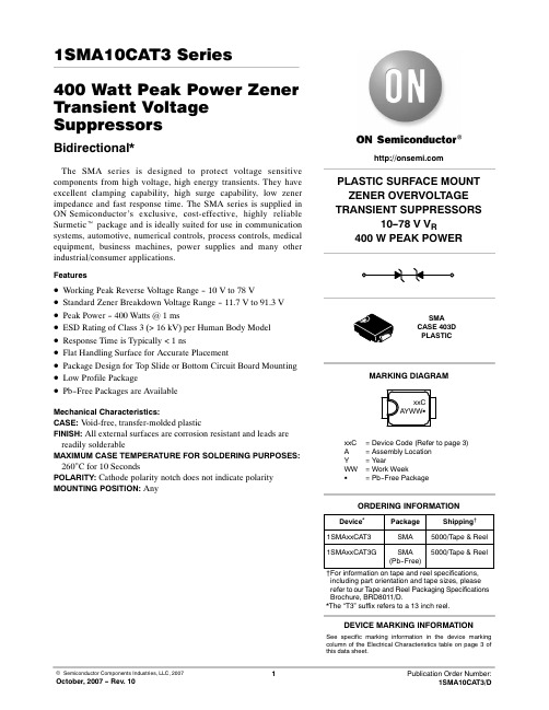
1SMA10CAT3 Series400 Watt Peak Power Zener Transient Voltage SuppressorsBidirectional*The SMA series is designed to protect voltage sensitive components from high voltage, high energy transients. They have excellent clamping capability, high surge capability, low zener impedance and fast response time. The SMA series is supplied in ON Semiconductor's exclusive, cost‐effective, highly reliable Surmetic t package and is ideally suited for use in communication systems, automotive, numerical controls, process controls, medical equipment, business machines, power supplies and many other industrial/consumer applications.Features•ăWorking Peak Reverse V oltage Range - 10 V to 78 V•ăStandard Zener Breakdown V oltage Range - 11.7 V to 91.3 V •ăPeak Power - 400 Watts @ 1 ms•ăESD Rating of Class 3 (> 16 kV) per Human Body Model•ăResponse Time is Typically < 1 ns•ăFlat Handling Surface for Accurate Placement•ăPackage Design for Top Slide or Bottom Circuit Board Mounting •ăLow Profile Package•ăPb-Free Packages are AvailableMechanical Characteristics:CASE:V oid‐free, transfer‐molded plasticFINISH:All external surfaces are corrosion resistant and leads are readily solderableMAXIMUM CASE TEMPERATURE FOR SOLDERING PURPOSES: 260°C for 10 SecondsPOLARITY:Cathode polarity notch does not indicate polarity MOUNTING POSITION:AnyPLASTIC SURFACE MOUNTZENER OVERVOLTAGE TRANSIENT SUPPRESSORS10-78 V V R400 W PEAK POWERDevice*Package Shipping†ORDERING INFORMATION1SMAxxCAT3SMA5000/T ape & ReelSMACASE 403DPLASTICMARKING DIAGRAM1SMAxxCAT3G SMA(Pb-Free)5000/T ape & Reel†For information on tape and reel specifications, including part orientation and tape sizes, please refer to our T ape and Reel Packaging Specifications Brochure, BRD8011/D.*The “T3” suffix refers to a 13 inch reel.See specific marking information in the device marking column of the Electrical Characteristics table on page 3 of this data sheet.DEVICE MARKING INFORMATIONxxC= Device Code (Refer to page 3)A= Assembly LocationY= YearWW= Work WeekG= Pb-Free PackagexxCAYWW GMAXIMUM RATINGSRatingSymbol Value Unit Peak Power Dissipation (Note 1)@ T L = 25°C, Pulse Width = 1 ms P PK 400W DC Power Dissipation @ T L = 75°C Measured Zero Lead Length (Note 2)Derate Above 75°CThermal Resistance from Junction-to-Lead P D R q JL 1.52050W mW/°C °C/W DC Power Dissipation (Note 3) @ T A = 25°C Derate Above 25°CThermal Resistance from Junction-to-Ambient P D R q JA 0.54.0250W mW/°C °C/W Operating and Storage Temperature RangeT J , T stg-65 to +150°CStresses exceeding Maximum Ratings may damage the device. Maximum Ratings are stress ratings only. Functional operation above the Recommended Operating Conditions is not implied. Extended exposure to stresses above the Recommended Operating Conditions may affect device reliability.1.10 X 1000 m s, non-repetitive.2. 1 in square copper pad, FR-4 board.3.FR-4 board, using ON Semiconductor minimum recommended footprint, as shown in 403B case outline dimensions spec.ELECTRICAL CHARACTERISTICS(T A = 25°C unless otherwise noted)Symbol ParameterI PP Maximum Reverse Peak Pulse Current V C Clamping Voltage @ I PP V RWM Working Peak Reverse VoltageI R Maximum Reverse Leakage Current @ V RWM V BR Breakdown Voltage @ I T I TTest CurrentELECTRICAL CHARACTERISTICSDevice*DeviceMarkingV RWM(Note 4)I R@ V RWMBreakdown VoltageV C @ I PP(Note 6)C Typ.(Note 7)V BR(Volts) (Note 5)@ I T V C I PPVolts m A Min Nom Max mA Volts Amps pF1SMA10CAT3, G QXC10 2.511.111.6912.27 1.017.023.5580 1SMA11CAT3, G QZC11 2.512.212.8413.48 1.018.222.0530 1SMA12CAT3, G REC12 2.513.314.0014.70 1.019.920.1490 1SMA13CAT3, G RGC13 2.514.415.1615.92 1.021.518.64551SMA14CAT3, G RKC14 2.515.616.4217.24 1.023.217.2425 1SMA15CAT3, G RMC15 2.516.717.5818.46 1.024.416.4400 1SMA16CAT3, G RPC16 2.517.818.7419.67 1.026.015.4375 1SMA18CAT3, G RTC18 2.52021.0622.11 1.029.213.7335 1SMA20CAT3, G RVC20 2.522.223.3724.54 1.032.412.3305 1SMA22CAT3, G RXC22 2.524.425.6926.97 1.035.511.3280 1SMA24CAT3, G RZC24 2.526.728.1129.51 1.038.910.32601SMA26CAT3, G SEC26 2.528.930.4231.94 1.042.19.5240 1SMA28CAT3, G SGC28 2.531.132.7434.37 1.045.48.8225 1SMA30CAT3, G SKC30 1.033.335.0636.81 1.048.48.3210 1SMA33CAT3, G SMC33 2.536.738.6340.56 1.053.37.5190 1SMA36CAT3, G SPC36 2.54042.1144.21 1.058.1 6.9175 1SMA40CAT3, G SRC40 2.544.446.7449.07 1.064.5 6.2160 1SMA43CAT3, G STC43 2.547.850.3252.83 1.069.4 5.8150 1SMA48CAT3, G SXC48 2.553.356.1158.91 1.077.4 5.2135 1SMA51CAT3, G SZC51 2.556.759.6962.67 1.082.4 4.9130 1SMA54CAT3, G TEC54 2.56063.1666.32 1.087.1 4.6120 1SMA58CAT3, G TGC58 2.564.467.7971.18 1.093.6 4.31151SMA60CAT3, G TKC60 2.566.770.2173.72 1.096.8 4.1110 1SMA64CAT3, G TMC64 2.571.174.8478.58 1.0103 3.9105 1SMA70CAT3, G TPC70 2.577.881.9085.99 1.0113 3.595 1SMA78CAT3, G TTC78 2.586.791.2795.83 1.0126 3.2904. A transient suppressor is normally selected according to the working peak reverse voltage (V RWM), which should be equal to or greater thanthe DC or continuous peak operating voltage level5.V BR measured at pulse test current I T at an ambient temperature of 25°C6.Surge current waveform per Figure 2 and derate per Figure 37.Bias voltage = 0 V, F = 1.0 MHz, T J = 25°C.†Please see 1SMA5.0AT3 to 1SMA78AT3 for Unidirectional devices.*The “G” suffix indicates Pb-Free package available.RATING AND TYPICAL CHARACTERISTIC CURVESFigure 1. Pulse Rating Curvet P , PULSE WIDTH (ms)P p k , P E A K P O W E R (k W )Figure 2. Pulse Waveformt, TIME (ms)I p p m , P E A K P U L S E C U R R E N T (%)Figure 3. Pulse Derating Curve1201008060400T A , AMBIENT TEMPERATURE (°C)P E A K P U L S E D E R A T I N G I N % O F 20P E A K P O W E R O R C U R R E N T1001110100BIAS VOLTAGE (VOLTS)Figure 4. Typical Junction Capacitance vs.Bias VoltageC , C A P A C I T A N C E (p F )10PACKAGE DIMENSIONSSMACASE 403D-02ISSUE DDIM A MIN NOM MAX MINMILLIMETERS1.922.17 2.270.076INCHES A10.050.100.150.002b 1.27 1.45 1.630.050c 0.150.280.410.006D 2.29 2.60 2.920.090E 4.06 4.32 4.570.160L0.761.14 1.520.0300.0850.0890.0040.0060.0570.0640.0110.0160.1030.1150.1700.1800.0450.060NOM MAX 4.83 5.21 5.590.1900.2050.220H E NOTES:1.DIMENSIONING AND TOLERANCING PER ANSI Y14.5M, 1982.2.CONTROLLING DIMENSION: INCH.3.403D-01 OBSOLETE, NEW STANDARD IS 403D-02.(SEE STYLES)ǒmm inchesǓSCALE 8:1*For additional information on our Pb-Free strategy and solderingdetails, please download the ON Semiconductor Soldering and Mounting Techniques Reference Manual, SOLDERRM/D.SOLDERING FOOTPRINT*ON Semiconductor and are registered trademarks of Semiconductor Components Industries, LLC (SCILLC). SCILLC reserves the right to make changes without further notice to any products herein. SCILLC makes no warranty, representation or guarantee regarding the suitability of its products for any particular purpose, nor does SCILLC assume any liability arising out of the application or use of any product or circuit, and specifically disclaims any and all liability, including without limitation special, consequential or incidental damages.“Typical” parameters which may be provided in SCILLC data sheets and/or specifications can and do vary in different applications and actual performance may vary over time. All operating parameters, including “Typicals” must be validated for each customer application by customer's technical experts. SCILLC does not convey any license under its patent rights nor the rights of others. SCILLC products are not designed, intended, or authorized for use as components in systems intended for surgical implant into the body, or other applications intended to support or sustain life, or for any other application in which the failure of the SCILLC product could create a situation where personal injury or death may occur. Should Buyer purchase or use SCILLC products for any such unintended or unauthorized application, Buyer shall indemnify and hold SCILLC and its officers, employees, subsidiaries, affiliates,and distributors harmless against all claims, costs, damages, and expenses, and reasonable attorney fees arising out of, directly or indirectly, any claim of personal injury or death associated with such unintended or unauthorized use, even if such claim alleges that SCILLC was negligent regarding the design or manufacture of the part. SCILLC is an Equal Opportunity/Affirmative Action Employer. This literature is subject to all applicable copyright laws and is not for resale in any manner.PUBLICATION ORDERING INFORMATIONSURMETIC is a trademark of Semiconductor Components Industries, LLC.。
B340A中文资料_数据手册_参数

N E W P R O D U C TProduct SummaryDescription and ApplicationsThe schottky rectifier providing low V F and excellent reverse leakage stability at high temperatures, this device is ideal for use in general rectification applications such as:∙ Boost Diode ∙ Blocking Diode ∙ Recirculating DiodeFeatures and Benefits∙ Reduced Low Forward Voltage Drop (V F ); Better Efficiency and Cooler Operation∙Reduced High-temperature Reverse Leakage; Increased Reliability against Thermal Runaway Failure in High Temperature Operation.∙ Lead-Free Finish; RoHS Compliant (Notes 1 & 2)∙ Halogen and Antimony Free. “Green” Device (Note 3)Mechanical Data∙ Case: SMA∙ Case Material: M olded Plastic, “Green” Molding Compound. UL Flammability Classification Rating 94V-0 ∙ Moisture Sensitivity: Level 1 per J-STD-020∙ Terminals: Finish - Matte Tin Annealed over Copper Leadframe. Solderable per MIL-STD-202, Method 208 ∙ Polarity: Cathode Band∙Weight: 0.063 grams (Approximate)Notes: 1. EU Directive 2002/95/EC (RoHS) & 2011/65/EU (RoHS 2) compliant. All applicable RoHS exemptions applied.2. See /quality/lead_free.html for more information about Diodes Incorporated’s definitions of Hal ogen- and Antimony-free, "Green" and Lead-free.3. Halogen- and Antimony-free "Green” products are defined as those which contain <900ppm bromine, <900ppm chlorine (<1500ppm total Br + Cl) and <1000ppm antimony compounds.4. For packaging details, go to our website at /products/packages.html.Marking InformationB3XXAE = Product Type Marking Code, ex: B320AE= Manufacturers’ Code Marking YWW = Date Code MarkingY = Last Digit of Year (ex: 6 for 2016) WW = Week Code (01 to 53)Top ViewSMABottom ViewB3XXAEGreenN E W P R O D U C TMaximum Ratings (@T A = +25°C, unless otherwise specified.)Single phase, half wave, 60Hz, resistive or inductive load.Thermal CharacteristicsNotes: 5. Device mounted on FR-4 substrate, 1"*1", 2oz, single-sided, PC boards with 0.56"*0.73" copper pad.6. Short duration pulse test used to minimize self-heating effect.N E W P R O D U C TN E W P R O D U C TPackage Outline DimensionsPlease see /package-outlines.html for the latest version.SMASuggested Pad LayoutPlease see /package-outlines.html for the latest version.SMAN E W P R O D U C T万联芯城专注电子元器件配单服务,只售原装现货库存,万联芯城电子元器件全国供应,专为终端生产,研发企业提供现货物料,价格优势明显,BOM配单采购可节省逐个搜索购买环节,只需提交BOM物料清单,商城即可为您报价,万联芯城现货库存销售能够满足多种客户的物料需求,一站式报价为客户节省采购成本,点击进入万联芯城。
MYG压敏电阻资料
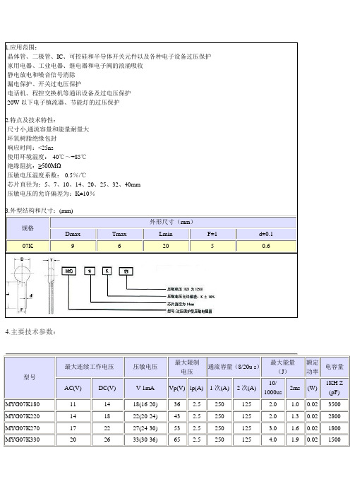
300
360(324-396)
595
10
1200
600
32
23
0.25
140
MYG07K391
250
320
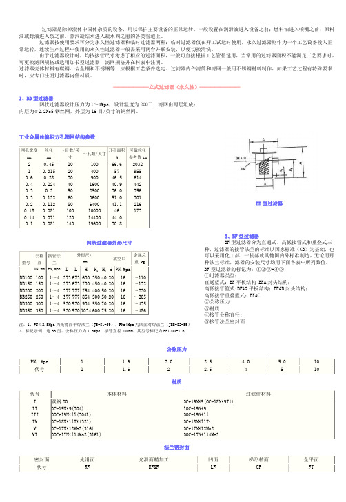
390(351-429)
650
10
1200
600
35
25
0.25
130
MYG07K431
275
350
430(387-473)
710
10
1200
600
40
27.5
0.25
115
MYG07K471
175
225
270(243-297)
455
10
1200
600
24
17
0.25
185
MYG07K301
190
250
300(270-330)
500
10
1200
600
26
18.5
0.25
165
MYG07K331
210
275
330(297-363)
550
10
1200
600
28
20
0.25
150
MYG07K361
36
2.5
250
125
2.0
1.0
0.02
3500
MYG07K220
14
18
22(20-24)
43
2.5
250
125
2.0
1.3
0.02
2800
MYG07K270
17
22
27(24-30)
53
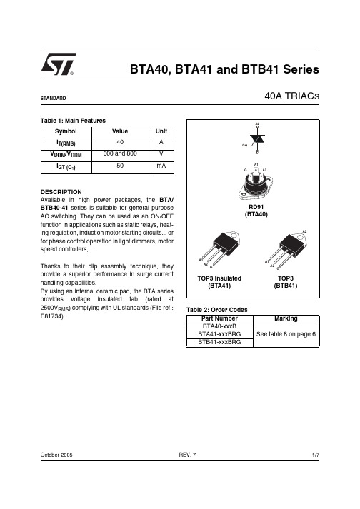
BTA40-700B中文资料
®1/7Table 1: Main FeaturesDESCRIPTIONAvailable in high power packages, the BTA/BTB40-41 series is suitable for general purpose AC switching. They can be used as an ON/OFF function in applications such as static relays, heat-ing regulation, induction motor starting circuits... or for phase control operation in light dimmers, motor speed controllers, ...Thanks to their clip assembly technique, they provide a superior performance in surge current handling capabilities.By using an internal ceramic pad, the BTA series provides voltage insulated tab (rated at 2500V RMS ) complying with UL standards (File ref.:E81734).Symbol Value Unit I T(RMS)40A V DRM /V RRM 600 and 800V I GT (Q 1)50mABTA40, BTA41 and BTB41 Series40A TRIAC SREV. 7October 2005STANDARDTable 2: Order CodesPart Number Marking BTA40-xxxB See table 8 on page 6BTA41-xxxBRG BTB41-xxxBRGBTA40, BTA41 and BTB41 Series2/7Table 3: Absolute Maximum Ratings Tables 4: Electrical Characteristics (T j = 25°C, unless otherwise specified)Table 5: Static Characteristics Symbol ParameterValue Unit I T(RMS)RMS on-state current (full sine wave)RD91 / TOP3T c = 95°C 40A TOP Ins.T c = 80°C I TSM Non repetitive surge peak on-state current (full cycle, T j initial = 25°C) F = 50 Hz t = 20 ms 400A F = 60 Hz t = 16.7 ms420I ²t I ²t Value for fusingt p = 10 ms 880A ²s dI/dtCritical rate of rise of on-state cur-rent I G = 2 x I GT , t r ≤ 100 nsF = 120 HzT j = 125°C 50A/µs V DSM /V RSM Non repetitive surge peak off-state voltaget p = 10 msT j = 25°C V DSM /V RSM + 100V I GM Peak gate currentt p = 20 µsT j = 125°C 8A P G(AV)Average gate power dissipation T j = 125°C1W T stg T jStorage junction temperature range Operating junction temperature range- 40 to + 150- 40 to + 125°CSymbol Test ConditionsQuadrant Value Unit I GT (1)V D = 12 V R L = 33 ΩI - II - III IV MAX.50100mA V GT ALL MAX. 1.3V V GD V D = V DRM R L = 3.3 k Ω T j = 125°C ALLMIN.0.2V I H (2)I T = 500 mA MAX.80mA I L I G = 1.2 I GTI - III - IVMAX.70mA II 160dV/dt (2)V D = 67 %V DRM gate openT j = 125°C MIN.500V/µs (dV/dt)c (2)(dI/dt)c = 20 A/msT j = 125°CMIN.10V/µsSymbol Test ConditionsValue Unit V T (2)I TM = 60 A t p = 380 µsT j = 25°C MAX. 1.55V V t0 (2)Threshold voltage T j = 125°C MAX.0.85V R d (2)Dynamic resistance T j = 125°C MAX.10m ΩI DRM I RRMV DRM = V RRMT j = 25°C MAX.5µA T j = 125°C5mANote 1: minimum I GT is guaranted at 5% of I GT max.Note 2: for both polarities of A2 referenced to A1.BTA40, BTA41 and BTB41 Series3/7Table 6: Thermal resistance Symbol ParameterValue Unit R th(j-c)Junction to case (AC)RD91 (Insulated) / TOP30.9°C/W TOP3 Insulated 0.6R th(j-a)Junction to ambientTOP3 / TOP3 Insulated50°C/WS = Copper surface under tab.Figure 1: Maximum power dissipation versus RMS on-state current (full cycle)Figure 2: RMS on-state current versus case temperature (full cycle)Figure 3: Relative variation of thermal impedance versus pulse durationFigure 4: On-state characteristics (maximumvalues)BTA40, BTA41 and BTB41 Series4/7Figure 5: Surge peak on-state current versus number of cyclesFigure 6: Non-repetitive surge peak on-state current for a sinusoidal pulse with width t p < 10 ms and corresponding value of I 2tFigure 7: Relative variation of gate trigger current, holding current and latching current versus junction temperature (typical values)Figure 8: Relative variation of critical rate of decrease of main current versus (dV/dt)c (typical values)Figure 9: Relative variation of critical rate of decrease of main current versus (dV/dt)cBTA40, BTA41 and BTB41 Series5/7Figure 10: Ordering Information SchemeTable 7: Product SelectorPart Numbers Voltage (xxx)Sensitivity Type Package 600 V 800 V BTA40-xxxB X X 50 mA Standard RD91BTA41-xxxBRG X X 50 mA Standard TOP3 Ins.BTB41-xxxBRGXX50 mAStandardTOP3BTB: non insulated TOP3 packageBTA40, BTA41 and BTB41 Series6/7In order to meet environmental requirements, ST offers these devices in ECOPACK® packages. These packages have a Lead-free second level interconnect . The category of second level interconnect is marked on the package and on the inner box label, in compliance with JEDEC Standard JESD97. The maximum ratings related to soldering conditions are also marked on the inner box label. ECOPACK is an ST trademark. ECOPACK specifications are available at: .Table 8: Ordering InformationOrdering type Marking Package Weight Base qtyDelivery modeBTA40-xxxB BTA40xxxB RD9120 g 25Bulk BTA41-xxxBRG BTA41xxxB TOP3 Ins. 4.5 g 30Tube BTB41-xxxBRGBTB41xxxBTOP34.5 g30TubeNote: xxx = voltageTable 9: Revision HistoryDate RevisionDescription of ChangesSep-20035Last update.25-Mar-20056TOP3 delivery mode changed from bulk to tube.14-Oct-20057T c values for I T changed in Table 3. ECOPACK statement added.BTA40, BTA41 and BTB41 Series Information furnished is believed to be accurate and reliable. However, STMicroelectronics assumes no responsibility for the consequencesof use of such information nor for any infringement of patents or other rights of third parties which may result from its use. No license is granted by implication or otherwise under any patent or patent rights of STMicroelectronics. Specifications mentioned in this publication are subject to change without notice. This publication supersedes and replaces all information previously supplied. STMicroelectronics products are notauthorized for use as critical components in life support devices or systems without express written approval of STMicroelectronics.The ST logo is a registered trademark of STMicroelectronics.All other names are the property of their respective owners© 2005 STMicroelectronics - All rights reservedSTMicroelectronics group of companiesAustralia - Belgium - Brazil - Canada - China - Czech Republic - Finland - France - Germany - Hong Kong - India - Israel - Italy - Japan - Malaysia - Malta - Morocco - Singapore - Spain - Sweden - Switzerland - United Kingdom - United States of America7/7。
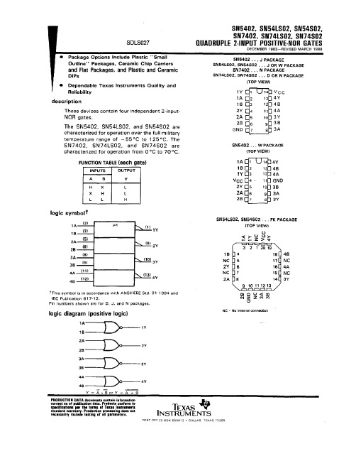
JM38510-00401BCA中文资料
PACKAGING INFORMATIONOrderable Device Status(1)PackageType PackageDrawingPins PackageQtyEco Plan(2)Lead/Ball Finish MSL Peak Temp(3)JM38510/00401BCA ACTIVE CDIP J141TBD Call TI Level-NC-NC-NCJM38510/00401BDA ACTIVE CFP W141TBD Call TI Level-NC-NC-NCJM38510/00401BDA ACTIVE CFP W141TBD Call TI Level-NC-NC-NCJM38510/07301BCA ACTIVE CDIP J141TBD Call TI Level-NC-NC-NCJM38510/07301BCA ACTIVE CDIP J141TBD Call TI Level-NC-NC-NCJM38510/07301BDA ACTIVE CFP W141TBD Call TI Level-NC-NC-NCJM38510/07301BDA ACTIVE CFP W141TBD Call TI Level-NC-NC-NCJM38510/30301B2A ACTIVE LCCC FK201TBD Call TI Level-NC-NC-NCJM38510/30301B2A ACTIVE LCCC FK201TBD Call TI Level-NC-NC-NCJM38510/30301BCA ACTIVE CDIP J141TBD Call TI Level-NC-NC-NCJM38510/30301BCA ACTIVE CDIP J141TBD Call TI Level-NC-NC-NCJM38510/30301BDA ACTIVE CFP W141TBD Call TI Level-NC-NC-NCJM38510/30301BDA ACTIVE CFP W141TBD Call TI Level-NC-NC-NCJM38510/30301SCA ACTIVE CDIP J141TBD Call TI Level-NC-NC-NCJM38510/30301SCA ACTIVE CDIP J141TBD Call TI Level-NC-NC-NCJM38510/30301SDA ACTIVE CFP W141TBD Call TI Level-NC-NC-NCJM38510/30301SDA ACTIVE CFP W141TBD Call TI Level-NC-NC-NC SN5402J ACTIVE CDIP J141TBD Call TI Level-NC-NC-NC SN5402J ACTIVE CDIP J141TBD Call TI Level-NC-NC-NC SN54LS02J ACTIVE CDIP J141TBD Call TI Level-NC-NC-NC SN54LS02J ACTIVE CDIP J141TBD Call TI Level-NC-NC-NC SN54S02J ACTIVE CDIP J141TBD Call TI Level-NC-NC-NC SN54S02J ACTIVE CDIP J141TBD Call TI Level-NC-NC-NC SN7402N ACTIVE PDIP N1425Pb-Free(RoHS)CU NIPDAU Level-NC-NC-NCSN7402N ACTIVE PDIP N1425Pb-Free(RoHS)CU NIPDAU Level-NC-NC-NC SN7402N3OBSOLETE PDIP N14TBD Call TI Call TISN7402N3OBSOLETE PDIP N14TBD Call TI Call TISN7402NE4ACTIVE PDIP N1425Pb-Free(RoHS)CU NIPDAU Level-NC-NC-NCSN7402NE4ACTIVE PDIP N1425Pb-Free(RoHS)CU NIPDAU Level-NC-NC-NCSN74LS02D ACTIVE SOIC D1450Green(RoHS&no Sb/Br)CU NIPDAU Level-1-260C-UNLIMSN74LS02D ACTIVE SOIC D1450Green(RoHS&no Sb/Br)CU NIPDAU Level-1-260C-UNLIMSN74LS02DE4ACTIVE SOIC D1450Green(RoHS&no Sb/Br)CU NIPDAU Level-1-260C-UNLIMSN74LS02DE4ACTIVE SOIC D1450Green(RoHS&no Sb/Br)CU NIPDAU Level-1-260C-UNLIMSN74LS02DR ACTIVE SOIC D142500Green(RoHS&no Sb/Br)CU NIPDAU Level-1-260C-UNLIMSN74LS02DR ACTIVE SOIC D142500Green(RoHS&no Sb/Br)CU NIPDAU Level-1-260C-UNLIMOrderable Device Status(1)PackageType PackageDrawingPins PackageQtyEco Plan(2)Lead/Ball Finish MSL Peak Temp(3)SN74LS02DRE4ACTIVE SOIC D142500Green(RoHS&no Sb/Br)CU NIPDAU Level-1-260C-UNLIMSN74LS02DRE4ACTIVE SOIC D142500Green(RoHS&no Sb/Br)CU NIPDAU Level-1-260C-UNLIM SN74LS02J OBSOLETE CDIP J14TBD Call TI Call TISN74LS02J OBSOLETE CDIP J14TBD Call TI Call TISN74LS02N ACTIVE PDIP N1425Pb-Free(RoHS)CU NIPDAU Level-NC-NC-NCSN74LS02N ACTIVE PDIP N1425Pb-Free(RoHS)CU NIPDAU Level-NC-NC-NC SN74LS02N3OBSOLETE PDIP N14TBD Call TI Call TISN74LS02N3OBSOLETE PDIP N14TBD Call TI Call TISN74LS02NE4ACTIVE PDIP N1425Pb-Free(RoHS)CU NIPDAU Level-NC-NC-NCSN74LS02NE4ACTIVE PDIP N1425Pb-Free(RoHS)CU NIPDAU Level-NC-NC-NCSN74LS02NSR ACTIVE SO NS142000Green(RoHS&no Sb/Br)CU NIPDAU Level-1-260C-UNLIMSN74LS02NSR ACTIVE SO NS142000Green(RoHS&no Sb/Br)CU NIPDAU Level-1-260C-UNLIMSN74LS02NSRG4ACTIVE SO NS142000Green(RoHS&no Sb/Br)CU NIPDAU Level-1-260C-UNLIMSN74LS02NSRG4ACTIVE SO NS142000Green(RoHS&no Sb/Br)CU NIPDAU Level-1-260C-UNLIMSN74S02D ACTIVE SOIC D1450Green(RoHS&no Sb/Br)CU NIPDAU Level-1-260C-UNLIMSN74S02D ACTIVE SOIC D1450Green(RoHS&no Sb/Br)CU NIPDAU Level-1-260C-UNLIMSN74S02DE4ACTIVE SOIC D1450Green(RoHS&no Sb/Br)CU NIPDAU Level-1-260C-UNLIMSN74S02DE4ACTIVE SOIC D1450Green(RoHS&no Sb/Br)CU NIPDAU Level-1-260C-UNLIM SN74S02DR OBSOLETE SOIC D14TBD Call TI Call TISN74S02DR OBSOLETE SOIC D14TBD Call TI Call TISN74S02N ACTIVE PDIP N1425Pb-Free(RoHS)CU NIPDAU Level-NC-NC-NCSN74S02N ACTIVE PDIP N1425Pb-Free(RoHS)CU NIPDAU Level-NC-NC-NC SN74S02N3OBSOLETE PDIP N14TBD Call TI Call TISN74S02N3OBSOLETE PDIP N14TBD Call TI Call TISN74S02NE4ACTIVE PDIP N1425Pb-Free(RoHS)CU NIPDAU Level-NC-NC-NCSN74S02NE4ACTIVE PDIP N1425Pb-Free(RoHS)CU NIPDAU Level-NC-NC-NC SNJ5402J ACTIVE CDIP J141TBD Call TI Level-NC-NC-NC SNJ5402J ACTIVE CDIP J141TBD Call TI Level-NC-NC-NC SNJ5402W ACTIVE CFP W141TBD Call TI Level-NC-NC-NC SNJ5402W ACTIVE CFP W141TBD Call TI Level-NC-NC-NC SNJ54LS02FK ACTIVE LCCC FK201TBD Call TI Level-NC-NC-NCOrderable Device Status(1)PackageType PackageDrawingPins PackageQtyEco Plan(2)Lead/Ball Finish MSL Peak Temp(3)SNJ54LS02FK ACTIVE LCCC FK201TBD Call TI Level-NC-NC-NC SNJ54LS02J ACTIVE CDIP J141TBD Call TI Level-NC-NC-NC SNJ54LS02J ACTIVE CDIP J141TBD Call TI Level-NC-NC-NC SNJ54LS02W ACTIVE CFP W141TBD Call TI Level-NC-NC-NC SNJ54LS02W ACTIVE CFP W141TBD Call TI Level-NC-NC-NC SNJ54S02FK ACTIVE LCCC FK201TBD Call TI Level-NC-NC-NC SNJ54S02FK ACTIVE LCCC FK201TBD Call TI Level-NC-NC-NCSNJ54S02J ACTIVE CDIP J141TBD Call TI Level-NC-NC-NCSNJ54S02J ACTIVE CDIP J141TBD Call TI Level-NC-NC-NCSNJ54S02W ACTIVE CFP W141TBD Call TI Level-NC-NC-NCSNJ54S02W ACTIVE CFP W141TBD Call TI Level-NC-NC-NC(1)The marketing status values are defined as follows:ACTIVE:Product device recommended for new designs.LIFEBUY:TI has announced that the device will be discontinued,and a lifetime-buy period is in effect.NRND:Not recommended for new designs.Device is in production to support existing customers,but TI does not recommend using this part in a new design.PREVIEW:Device has been announced but is not in production.Samples may or may not be available.OBSOLETE:TI has discontinued the production of the device.(2)Eco Plan-The planned eco-friendly classification:Pb-Free(RoHS)or Green(RoHS&no Sb/Br)-please check /productcontent for the latest availability information and additional product content details.TBD:The Pb-Free/Green conversion plan has not been defined.Pb-Free(RoHS):TI's terms"Lead-Free"or"Pb-Free"mean semiconductor products that are compatible with the current RoHS requirements for all6substances,including the requirement that lead not exceed0.1%by weight in homogeneous materials.Where designed to be soldered at high temperatures,TI Pb-Free products are suitable for use in specified lead-free processes.Green(RoHS&no Sb/Br):TI defines"Green"to mean Pb-Free(RoHS compatible),and free of Bromine(Br)and Antimony(Sb)based flame retardants(Br or Sb do not exceed0.1%by weight in homogeneous material)(3)MSL,Peak Temp.--The Moisture Sensitivity Level rating according to the JEDEC industry standard classifications,and peak solder temperature.Important Information and Disclaimer:The information provided on this page represents TI's knowledge and belief as of the date that it is provided.TI bases its knowledge and belief on information provided by third parties,and makes no representation or warranty as to the accuracy of such information.Efforts are underway to better integrate information from third parties.TI has taken and continues to take reasonable steps to provide representative and accurate information but may not have conducted destructive testing or chemical analysis on incoming materials and chemicals.TI and TI suppliers consider certain information to be proprietary,and thus CAS numbers and other limited information may not be available for release.In no event shall TI's liability arising out of such information exceed the total purchase price of the TI part(s)at issue in this document sold by TI to Customer on an annual basis.元器件交易网IMPORTANT NOTICETexas Instruments Incorporated and its subsidiaries (TI) reserve the right to make corrections, modifications, enhancements, improvements, and other changes to its products and services at any time and to discontinue any product or service without notice. Customers should obtain the latest relevant information before placing orders and should verify that such information is current and complete. All products are sold subject to TI’s terms and conditions of sale supplied at the time of order acknowledgment.TI warrants performance of its hardware products to the specifications applicable at the time of sale in accordance with TI’s standard warranty. T esting and other quality control techniques are used to the extent TI deems necessary to support this warranty. Except where mandated by government requirements, testing of all parameters of each product is not necessarily performed.TI assumes no liability for applications assistance or customer product design. Customers are responsible for their products and applications using TI components. T o minimize the risks associated with customer products and applications, customers should provide adequate design and operating safeguards.TI does not warrant or represent that any license, either express or implied, is granted under any TI patent right, copyright, mask work right, or other TI intellectual property right relating to any combination, machine, or process in which TI products or services are used. Information published by TI regarding third-party products or services does not constitute a license from TI to use such products or services or a warranty or endorsement thereof. Use of such information may require a license from a third party under the patents or other intellectual property of the third party, or a license from TI under the patents or other intellectual property of TI.Reproduction of information in TI data books or data sheets is permissible only if reproduction is without alteration and is accompanied by all associated warranties, conditions, limitations, and notices. Reproduction of this information with alteration is an unfair and deceptive business practice. TI is not responsible or liable for such altered documentation.Resale of TI products or services with statements different from or beyond the parameters stated by TI for that product or service voids all express and any implied warranties for the associated TI product or service and is an unfair and deceptive business practice. TI is not responsible or liable for any such statements. Following are URLs where you can obtain information on other Texas Instruments products and application solutions:Products ApplicationsAmplifiers Audio /audioData Converters Automotive /automotiveDSP Broadband /broadbandInterface Digital Control /digitalcontrolLogic Military /militaryPower Mgmt Optical Networking /opticalnetwork Microcontrollers Security /securityTelephony /telephonyVideo & Imaging /videoWireless /wirelessMailing Address:Texas InstrumentsPost Office Box 655303 Dallas, Texas 75265Copyright 2005, Texas Instruments Incorporated。
T73YB5KTR750中文资料
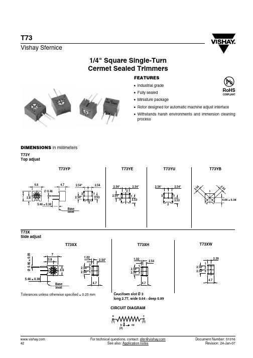
1/4" Square Single-Turn Cermet Sealed Trimmers For technical questions, contact: sfer@Document Number: 5101642See also: Application notesRevision: 24-Jan-07T73Vishay SferniceFEATURES•Industrial grade •Fully sealed •Miniature package•Rotor designed for automatic machine adjust interface •Withstands harsh environments and immersion cleaningprocessDIMENSIONS in millimetersT73YTop adjustT73YPT73YET73YUT73YBT73XSide adjustT73XXT73XHT73XWTolerances unless otherwise specified ± 0.25 mmCruciform slot Ø 3long 2.77, wide 0.64 - deep 0.89CIRCUIT DIAGRAMDocument Number: 51016For technical questions, contact: sfer@Revision: 24-Jan-07See also: Application notes43T731/4" Square Single-Turn Cermet Sealed T rimmersVishay SferniceELECTRICAL SPECIFICATIONSResistive Element Cermet Electrical Travel 240° nominal Resistance Range 10 Ω to 2 M ΩStandard Series 1 - 2 - 5Tolerance Standard ± 10 %Power RatingLinear 0.5 W at 70 °C Logarithmicnot applicable Temperature Coefficient ± 100 ppm/°CLimiting Element Voltage 300 VContact Resistance Variation 1 % or 3Ω max. whichever is greater Absolute Minimum Resistance 1 % or 2 Ω max. whichever is greaterAdjustability ± 0.05 % voltage ± 0.15 % resistanceResolutioninfinite Insulation Resistance (500 V DC)103 M Ω minimum Dielectric Strength900 Vac sea level 350 Vac 80 000 feetMECHANICAL SPECIFICATIONSMechanical Travel270°Operating Torque (max. Ncm) 2.1End Stop Torque (max. Ncm) 4.9Unit Weight (max. g)0.6ENVIRONMENTAL SPECIFICATIONSTemperature Range - 55 °C to + 125 °C Climatic Category 55/100/56Seal Test 85 °C Fluorinert**Flammability UL 94-VO ** Fluorinert is a registered trademark of 3M Co.POWER RATING CHARTPERFORMANCETESTS CONDITIONSTYPICAL VALUES AND DRIFTS Load Life 1000 hours - 0.5 W at + 70 °CΔR R ≤ 3 %CRV < 3 Ω or 3 %whichever is greater Shock 100 g ΔR R < ± 1 %ΔV V < ± 1 %Vibration 30 gΔR R < ± 1 %ΔV V ≤ ± 1 %Humidity Mil-STD202 method 103 - 96 hoursΔR R < ± 2 %i.R. 10 M ΩRotational Life200 cyclesΔR R< ± 4 %CRV< 3 Ω or 3 %whichever is greater For technical questions, contact: sfer@Document Number: 5101644See also: Application notesRevision: 24-Jan-07T73Vishay Sfernice1/4" Square Single-T urn Cermet Sealed TrimmersMARKINGPrinted: VISHAY trademark, resistance code, terminal numbers, date code, manufacturer’s model number and styleSTANDARD RESISTANCE ELEMENT DATASTANDARD RESISTANCE VALUESLINEAR LAWTCR - 55 °C + 125 °C MAX.POWER AT 70 °C MAX.WORKING VOLTAGEMAX. WIPER CUR.ΩW V mA ppm/°C1020501002005001K 2K 5K 10K 20K 50K 100K 200K 500K 1M 2M0.50.500.450.180.090.052.23.257.11015.822.431.65070.7100158.1223.63003003003002241601007050322216107.153.22.21.50.600.300.15± 100PACKAGING- In tube by 50 pieces, code TU50- T ape and reel for model YU, code TR750 and XW, code TR100ORDERING INFORMATIONT73SERIESYP STYLE 500 k ΩOHMIC VALUE± 10 %TOLERANCETU50PACKAGING e3LEAD FINISH XX XH XWYP YE YU YBTU50On request: TR750TR1000e3: pure SnLegal Disclaimer NoticeVishay Document Number: Revision: 08-Apr-051NoticeSpecifications of the products displayed herein are subject to change without notice. Vishay Intertechnology, Inc., or anyone on its behalf, assumes no responsibility or liability for any errors or inaccuracies.Information contained herein is intended to provide a product description only. No license, express or implied, by estoppel or otherwise, to any intellectual property rights is granted by this document. Except as provided in Vishay's terms and conditions of sale for such products, Vishay assumes no liability whatsoever, and disclaims any express or implied warranty, relating to sale and/or use of Vishay products including liability or warranties relating to fitness for a particular purpose, merchantability, or infringement of any patent, copyright, or other intellectual property right. The products shown herein are not designed for use in medical, life-saving, or life-sustaining applications. Customers using or selling these products for use in such applications do so at their own risk and agree to fully indemnify Vishay for any damages resulting from such improper use or sale.。
MYG全系列标准中文新版规格书
C
1600 1300 1050 900 500 450 400 350 250 200 170 140
80 70 70 65 50 50 45 40
NANJING SHAGON ELECTRONICS CO.,LTD
表3
07 品种额定
型号规格
特性项目和额定值
压敏电 最大连续工作电
压(V)
压(V)
等级电压 等级电流 (V) (A)
μS
5
500 17
5
500 17
5
500 17
5
500 17
5
500 17
5
500 17
5
500 17
5
500 17
25
2500 30
25
2500 30
25
2500 30
25
2500 30
25
2500 30
25
2500 30
25
2500 30
25
2500 30
25
2500 30
25
2500 30
25
最大峰值电流 (A)
V
A·Crms D.C
Vc
MYG07K180
18
11
14
36
MYG07K220
22
14
18
43
MYG07K270
27
17
22
53
MYG07K330
33
20
26
65
MYG07K390
39
25
31
77
MYG07K470
47
30
38
93
MYG07K560
MC403 Power System及相关配件说明说明书

USA/ CanadaNEMA 5-15P AC male plugIEC 60320 C13 AC female connector SJT 18AWG*3C, 2m/78.7in (L)EuropeCEE 7/7 AC male plugIEC 60320 C13 AC female connector H05VV-F 0.75*3C, 2m/78.7in (L)JapanJIS C 8303 AC male plugIEC 60320 C13 AC female connector VCTF 0.75*3C, 2m/78.7in (L)AustraliaSAA power cord, AS3112 AC male plug, 10A IEC 60320 C13 AC female connector2m/78.7in (L)UKNEMA 5-15P AC male plugIEC 60320 C13 AC female connector H05VV-F 0.75*3C, 2m/78.7in (L)HARDWARE CHECKLISTUnpack the contents of the box and check that the following was included:One (1) MC403 Power SystemOne (1) MC403 instruction manualOne (1) 19” rack front panelTwo (2) pedalboard mounting bracketsTwenty (20) cables:F o u r (4) 2.1 x 5.5m m b l a c k r i g h t a n g l e t o s t r a i g h t, 1’ l o n gEight (8) 2.1 x 5.5mm black right angle to straight, 2’ longFour (4) 2.1 x 5.5mm black right angle to straight 3’ longTwo (2) 2.5 x 5.5mm red right angle to straight 4’ longOne (1) 2.1 x 5.5mm to 3.5mm black straight 2’ longOne (1) 2.1 x 5.5mm to 3.5mm black straight 3’ longOne (1) AC cord with appropriate connector for region of operation:DIRECTIONS(1) Set the red AC 115/230 input selector to your local AC voltage.(2) Plug the included AC power cord into the AC IN jack.(3) Connect the AC cord into a wall outlet.(4) Flip the ON/OFF switch to the ON position. A red LED on the rear panel will lightup to indicate the unit is active.(5) Read the OUTPUT GUIDE on the following pages to make sure you are using thecorrect output jacks and cables.(6) Connect pedals to the MC403 using supplied cables. The red LED aboveeach output jack will light to indicate that power is being supplied to theconnected pedal.(7) An AC THRU jack is located next to the AC IN jack to provide auxiliary powerto another device. DO NOT EXCEED 200 WATTS on AC THRU device!OUTPUT GUIDEBefore plugging anything into the MC403 Power System, check that the powerrequirements of the device match the output capabilities of the MC403.Specifically, you should check:(1) The device’s voltage requirement to match the MC403 output voltage.(2) Whether the device uses AC or DC.(3) The current requirement to not exceed the MC403’s MAX CURRENT spec.(4) The polarity when using DC power.The cables provided with the MC403support the industry standard positive (+)barrel and negative (-) center polarity.If you are unsure about what power your device requires,DO NOT PLUG THE DEVICE INTO THE MC403! The following list provides usageexamples for each of the output types available on the MC403.ADJUSTABLE DC OUTPUTS – Use 2.1 x 5.5mm black cables.Push the red button IN for the high voltage (10.5-15V) setting.Push the red button OUT for the low voltage (6.5-10.5V) setting.Rotate the black adjustment knob to fine tune the value.To simulate a dying battery tone on a transistor based distortion/fuzz/overdrive,set the red button OUT and rotate the adj. knob until desired tone is achieved.Radial™ Tonebone™ pedals requiring 15VDC, 400mA can be used with the redbutton IN and the adjustment knob rotated fully clockwise.9VAC OUTPUTS– Use 2.5 x 5.5mm red cables.Line 6® Stomp Modeler and POD® units (excluding Pocket POD®)9VDC OUTPUTS – Use 2.1 x 5.5mm black cables.MXR®, Crybaby®, Way Huge® Electronics pedals requiring Dunlop ECB-003Dunlop® UV1SC Stereo Chorus, JD4S RotovibeBoss® pedals requiring PSA-series adaptersElectro-Harmonix® pedals requiring 9DC-100 adapterMaxon® pedals requiring AC210N adapterIbanez® pedals requiring AC109 adapterRadial™ pedals requiring 9VDC, 40mA negative center adaptersLine6® ToneCore® series pedalsDigiTech® pedals requiring PSR200R18VDC OUTPUTS – Use 2.1 x 5.5mm black cables.MXR®, Crybaby® pedals requiring Dunlop ECB-004Dunlop® UV1 UnivibeFRONT PANEL & PEDAL BOARD BRACKET ASSEMBLYRemove the four screws on front of unit as indicated in Figure A for rack mountingor as in Figure B for pedalboard mounting. Place the brackets on the unit, line upthe holes, and replace screws to secure brackets. Use M3.0x0.5, L=8mm (max)screws if factory screws are lost.Figure B – Pedalboard MountFigure A – Rack Mount92503008461R E V CWARNING: READ THIS FIRST BEFORE OPERATING!(1)(2)(3)(4)(5)(6)(7)(8) (9) (10) (11)(12)(13) (14)。
MYG压敏电阻
395
84
8000 6000
30
14K271 270 243-297 175 225
455
99
8000 6000
30
高
14K331 330 297-363 210 275
550
115
8000 6000
30
能
14K361 360 324-396 230 300
595
130
8000 6000
30
I
14K391 390 351-429 250 320
1025
92
4600
3500
10K681 680 612-748 420 560
1120
92
4600
3500
10K751 750 675-825 460 615
1240
100
4600
3500
10K821 820 738-902 510 670
1355
110
4600
3500
浙江黄岩航洋电子有限公司 TEL:86-0576-84179098 FAX:86-0576-84173885 Email:hangyang@
300
15.6
2300
1750
通
07K201 200 185-225 130 170
340
17.5
2300
1750
型
07K221 220 198-242 140 180
360
19
2300
1750
07K241 240 216-264 150 200
395
21
2300
1750
07K271 270 243-297 175 225
BTA41-700B中文资料

BTA41A/B BTB41BMarch 1995STANDARD TRIACSSymbol ParameterValue Unit I T(RMS)RMS on-state current (360°conduction angle)BTA Tc =75°C 40ABTBTc =85°C 45I TSMNon repetitive surge peak on-state current (Tj initial =25°C )tp =8.3ms 315A tp =10ms 300I 2t I 2t valuetp =10ms 450A 2s dI/dtCritical rate of rise of on-state currentGate supply :I G =500mA di G /dt =1A/µsRepetitive F =50Hz 10A/µs Non Repetitive50Tstg Tj Storage and operating junction temperature range-40to +150-40to +125°C °C TlMaximum lead temperature for soldering during 10s at 4.5mm from case260°C TOP 3(Plastic)A1A2G.HIGH SURGE CURRENT CAPABILITY .COMMUTATION :(dV/dt)c >10V/µs .BTA Family :INSULATING VOLTAGE =2500V (RMS)(UL RECOGNIZED :E81734)DESCRIPTIONSymbol ParameterBTA41-...A/B /BTB41-...BUnit400600700800V DRM V RRM Repetitive peak off-state voltage Tj =125°C400600700800VABSOLUTE RATINGS (limiting values)FEATURESThe BTA41A/B /BTB41B triac family are high performance glass passivated PNPN devices.These parts are suitables for general purpose ap-plications where high surge current capability is re-quired.Application such as phase control and static switching on inductive or resistive load.1/5GATE CHARACTERISTICS (maximum values)Symbol ParameterValue Unit Rth (j-a)Junction to ambient50°C/W Rth (j-c )DC Junction to case for DCBTA 1.2°C/WBTB0.8Rth (j-c)AC Junction to case for 360°conduction angle(F=50Hz)BTA 0.9°C/W BTB0.6SymbolTest ConditionsQuadrantSuffixUnitAB I GTV D =12V(DC)R L =33ΩTj=25°CI-II-III MAX 10050mA IVMAX 150100V GT V D =12V(DC)R L =33ΩTj=25°C I-II-III-IV MAX 1.5V V GD V D =V DRM R L =3.3k ΩTj=125°C I-II-III-IV MIN 0.2V tgt V D =V DRM I G =500mA dI G /dt =3A/µs Tj=25°C I-II-III-IV TYP 2.5µs I LI G =1.2I GTTj=25°CI-III-IV TYP7060mA II200180I H *I T =500mA gate open Tj=25°C MAX 10080mA V TM *I TM =60A tp=380µs Tj=25°C MAX 1.8V I DRM I RRM V DRM Rated V RRMRatedTj=25°C MAX 0.01mATj=125°C MAX 6dV/dt *Linear slope up to V D =67%V DRM gate open Tj=125°CMIN250250V/µs(dV/dt)c *(dI/dt)c =18A/ms BTA (dI/dt)c =20A/msBTBTj=125°C MIN 10V/µs*For either polarity of electrode A 2voltage with reference to electrode A 1.P G (AV)=1WP GM =40W (tp =20µs)I GM =8A (tp =20µs)V GM =16V (tp =20µs).ELECTRICAL CHARACTERISTICSTHERMAL RESISTANCESBTA41A/B /BTB41B2/5ORDERING INFORMATIONPackage I T(RMS)V DRM/V RRM Sensitivity SpecificationA V A BBTA (Insulated)41400X X600X X700X X800X XBTB (Uninsulated)45400X600X700X800XFig.1:Maximum RMS power dissipation versus RMS on-state current(F=50Hz).(Curves are cut off by(dI/dt)c limitation)(BTA)Fig.2:Correlation between maximum RMS power dissipation and maximum allowable temperatures(T amb and T case)for different thermal resistances heatsink+ contact(BTA).Fig.3:Maximum RMS power dissipation versus RMS on-state current(F=50Hz).(Curves are cut off by(dI/dt)c limitation)(BTB)Fig.4:Correlation between maximum RMS power dissipation and maximum allowable temperatures(T amb and T case)for different thermal resistances heatsink+ contact(BTB).BTA41A/B/BTB41B3/5Fig.8:Relative variation of gate trigger current and holding current versus junction temperature.Fig.9:Non Repetitive surge peak on-state current versus number of cycles.Fig.10:Non repetitive surge peak on-state current for a sinusoidal pulse with width :t ≤ 10ms,and corresponding value of I 2t.1E-31E-21E-11E+01E+11E+21E+30.010.101.00Zth/Rth Zth(j-c)Zth(j-a)tp(s)Fig.7:Relative variation of thermal transient impedance pulse duration.Fig.5:RMS on-state current versus case temperature.(BTA)Fig.6:RMS on-state current versus case temperature.(BTB)BTA41A/B /BTB41B4/5Fig.11:On-state characteristics (maximum values).PACKAGE MECHANICAL DATA TOP 3PlasticCooling method :C Marking :type number Weight :4.7gRecommended torque value :0.8m.N.Maximum torqur value :1m.N.HR 4.6CAGDBPN NL MJIREF.DIMENSIONSMillimeters Inches Min.Max.Min.Max.A 15.1015.500.5940.611B20.7021.100.8140.831C 14.3015.600.5610.615D 16.1016.500.6320.650G 3.40-0.133-H 4.40 4.600.1730.182I 4.08 4.170.1610.164J1.45 1.550.0570.062L 0.500.700.0190.028M2.70 2.900.1060.115N 5.40 5.650.2120.223P1.201.400.0470.056Information furnished is believed to be accurate and reliable.However,SGS-THOMSON Microelectronics assumes no responsability for the consequences of use of such information nor for any infringement of patents or other rights of third parties which may result from its use.No license is granted by implication or otherwise under any patent or patent rights of SGS-THOMSON Microelectronics.Specifications mentioned in this publication are subject to change without notice.This publication supersedes and replaces all information previously supplied.SGS-THOMSON Microelectronics products are not authorized for use as critical components in life support devices or systems without express written approval of SGS-THOMSON Microelectronics.©1995SGS-THOMSON Microelectronics -Printed in Italy -All rights reserved.SGS-THOMSON Microelectronics GROUP OF COMPANIESAustralia -Brazil -France -Germany -Hong Kong -Italy -Japan -Korea -Malaysia -Malta -Morocco -The Nether-lands -Singapore -Spain -Sweden -Switzerland -Taiwan -Thailand -United Kingdom -U.S.A.BTA41A/B /BTB41B5/5。
SGB750
国电南自Q/GDNZ.JB101-2011SG B750数字式母线保护装置(智能站)说明书国电南京自动化股份有限公司GUODIAN NANJING AUTOMATION CO.,LTD安全声明为保证安全、正确、高效地使用装置,请务必阅读以下重要信息:1.装置的安装调试应由专业人员进行;2.装置上电使用前请仔细阅读说明书。
应遵照国家和电力行业相关规程,并参照说明书对装置进行操作、调整和测试。
如有随机材料,相关部分以资料为准;3.装置上电前,应明确连线与正确示图相一致;4.装置应该可靠接地;5.装置施加的额定操作电压应该与铭牌上标记的一致;6.严禁无防护措施触摸电子器件,严禁带电插拔模件;7.接触装置端子,要防止电触击;8.如要拆装装置,必须保证断开所有地外部端子连接,或者切除所有输入激励量。
否则,触及装置内部的带电部分,将可能造成人身伤害;9.对装置进行测试时,应使用可靠的测试仪;10.装置的运行参数和保护定值同样重要,应准确设定才能保证装置功能的正常运行;11.改变当前保护定值组将不可避免地要改变装置的运行状况,在改变前应谨慎,并按规程作校验;12.装置操作密码为:99。
版本声明产品说明书版本修改记录表1098 V1.07I 国网版装置系列化(智能站) V2.00G(I) 2011-057 V1.07 增加死区事件功能,增加故障详细信息功能V2.00G,V2.00G(XX)2010-046 V1.06 根据最新国网试验做相应修改V1.06g,V1.07g 2009-065 V1.05 根据国网标准做相应修改V1.05 2009-034 V1.04 增加IEC61850及数字化变电站部分V1.02 2008-013 V1.03 内容细化,便于理解V1.02 2007-102 V1.02 V1.0 2005-91 V1.01 V1.0 2004-12 序号说明书版本号修改摘要软件版本号修改日期* 技术支持电话:(025)51183084 51183086传真:(025)51183154* 本说明书可能会被修改,请注意核对实际产品与说明书的版本是否相符* 2011年05月第7版第1次印刷目录1 概述 (1)1.1适用范围 (1)1.2保护功能配置 (1)1.3原理特点 (1)1.4辅助功能及结构特点 (2)2 技术数据 (3)2.1额定电气参数 (3)2.2主要技术性能及指标 (3)2.3大气条件 (4)2.4电磁兼容性试验 (4)2.5绝缘和耐湿热性能 (5)2.6机械性能 (5)3 硬件说明 (6)3.1硬件结构说明 (6)3.2外部连接 (6)4 保护原理 (8)4.1母线差动保护 (8)4.2母联(分段)断路器失灵和盲区保护 (18)4.3自动识别充电状态功能 (21)4.4断路器失灵保护 (22)4.5复合电压闭锁与PT断线判别功能 (27)4.6双母线运行方式识别功能 (28)4.7母联(分段)充电过流保护 (30)4.8母联(分段)非全相保护 (31)4.9双A/D逻辑 (31)5 保护配置说明 (33)5.1母联兼旁路 (33)5.2旁路兼母联 (34)5.3母线兼旁路 (36)5.4双母线单分段(双母线三分段) (37)5.5双母线双分段 (38)6 保护整定说明 (40)6.1电流折算 (40)6.2保护整定项目及原则 (40)6.3整定值清单 (43)附录2:装置背板图及虚端子 (54)附录3:装置人机界面及菜单结构 (64)附录4:装置调试与运行 (72)附录5:SG B750装置支持的IEC 61850标准 (76)1 概述我公司针对110kV-750kV电力系统的特点,结合二十多年来在各电压等级母线保护领域内的理论研究成果及成功的现场运行实践经验,提出并采用一整套母线保护新判据,在全新的EDP-01嵌入式系统平台基础上开发研制成SG B750系列数字式母线保护装置。
MBR4040W中文资料
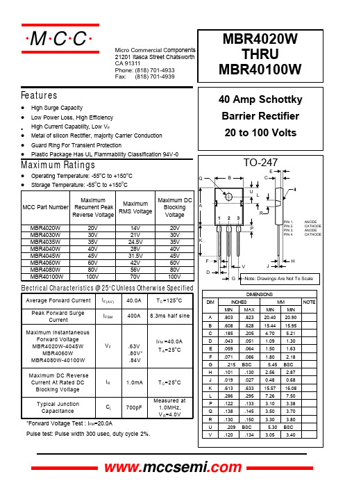
o
o
MCC Part Number
Maximum DC Blocking Voltage 20V 30V 35V 40V 45V 60V 80V 100V
A R 1 2 3 P K
PIN 1. PIN 2. PIN 3. PIN 4. ANODE CATHODE ANODE CATHODE
1
2
5
102050100CASE TEMPERATURE , C
NUMBER OF CYCLES AT 60Hz
FIG.3 - TYPICAL REVERSE CHARACTERISTICS
100
FIG.4 - TYPICAL FORWARD CHARACTERISTICS
100
INSTANTANEOUS FORWARD CURRENT ,(A)
DIMENSIONS
Average Forward Current Peak Forward Surge Current Maximum Instantaneous Forward Voltage MBR4020W-4045W MBR4060W MBR4080W-40100W Maximum DC Reverse Current At Rated DC Blocking Voltage Typical Junction Capacitance
MM MIN 20.90 15.95 5.21 1.30 1.63 2.18 BSC 2.87 0.68 16.08 7.50 3.38 3.70 3.80 BSC 3.40
NOTE
VF
.63V .80V* .84V
I FM =40.0A T A = 2 5o C
D E F G H J K L
MAA50-2K480512SBN中文资料
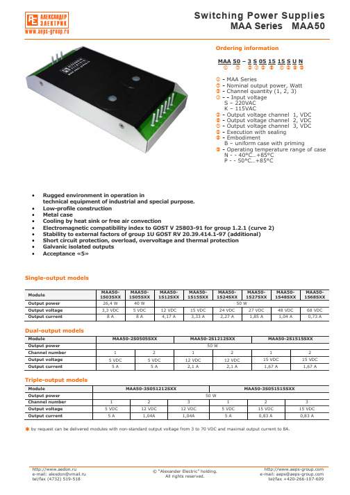
Single-output modelsModule МАА50- 1S03S ХХ МАА50- 1S05S ХХ МАА50- 1S12S ХХ МАА50- 1S15S ХХ МАА50- 1S24S ХХ МАА50- 1S27S ХХМАА50- 1S48S ХХ МАА50- 1S68S ХХ Output power 26,4 W 40 W 50 W Output voltage 3,3 VDC 5 VDC12 VDC15 VDC24 VDC27 VDC48 VDC68 VDCOutput current8 A8 А 4,17 А 3,33 А 2,27 А 1,85 А 1,04 А 0,73 АDual-output modelsModule МАА50-2S0505S ХХ МАА50-2S1212S ХХМАА50-2S1515S ХХOutput power 50 WChannel number 1 2 1 2 1 2 Output voltage 5 VDC 5 VDC 12 VDC 12 VDC15 VDC 15 VDC Output current5 А 5 А 2,1 А 2,1 А 1,67 А 1,67 АTriple-output modelsModule МАА50-3S051212S ХХМАА50-3S051515S ХХOutput power 50 WChannel number 1 2 3 1 2 3Output voltage 5 VDC12 VDC12 VDC5 VDC15 VDC15 VDCOutput current5 А 1,04А 1,04А 5 А 0,83 А 0,83 Аby request can be delivered modules with non-standard output voltage from 3 to 70 VDC and maximal output current to 8А.Ordering informationМАА 50 – 3 S 05 15 15 S U Nc d e f g h i j k lc - MAA Seriesd - Nominal output power, Watte - Channel quantity (1, 2, 3)f - - Input voltageS – 220VAC K – 115VACg - Output voltage channel 1, VDC h - Output voltage channel 2, VDC i - Output voltage channel 3, VDC j - Execution with sealing k - EmbodimentB – uniform case with primingl - Operating temperature range of caseN - - 40°С…+85°С P - - 50°С…+85°С• Rugged environment in operation intechnical equipment of industrial and special purpose. • Low-profile construction • Metal case• Cooling by heat sink or free air convection• Electromagnetic compatibility index to GOST V 25803-91 for group 1.2.1 (curve 2) • Stability to external factors of group 1U GOST RV 20.39.414.1-97 (additional) • Short circuit protection, overload, overvoltage and thermal protection • Galvanic isolated outputs •Acceptance «5»Температура окружающей среды Токр, С9080706050403020100-10-20-30-40-50Выходная мощность, Вт6050403020100Input specificationsParameter Conditions of dimensions MIN NOM MAX UnitS 187 220 242 VACSteady-state deviationК 80 115 140 VAC S 176 264 VACInput voltageTransient deflection, 1 secК 80 150 VAC SInput frequencyК47 400 440 HzOutput specificationsParameterConditions of dimensions MIN NOM MAX Unit Single-output execution (Inom 10 – 100%) ±3 % Output 1 multi-output execution(Inom 10 – 100%) ±3 %Uout2&3 differs from Uout1 less than 20% Output 2 and 3 multi-output execution(Inom 10 – 100%)±13 %Output 1 multi-output execution (Inom 30 – 100%) ±3 %Total output voltage instabilityUout2&3differs fromUout1 more than 20% Output 2 and 3 multi-output execution(Inom 50-100%) ±15 %Output voltage pulsations ripple(peak-to-peak)Dimension by device for pulsation control2% Uout.nom.Current overload protection actuation level110 % Iout.nom. Short circuit protection Autorepair 150 % Iout.nom. Overvoltage protection 120 % Uout.nom.Thermal protection90-95°CGeneral specificationsParameterConditions of dimensions MIN NOM MAX Unit- operating of case N P – 40 – 50 +85+85°C– power loss See diagram Temperature– storage – 50 +85 °CEfficiency 78 % Conversion frequency 50 kHz~ in/out 1500 VAC ~ in/case 1500 VAC~ out/case 500 VDC Isolation~ out/out 500 VDCInsulation resistance Voltage 500VDC 20 Ohm High humidity Temperature 35°С 98 % Cyclic overpatching of temperature – 60 +85 °C Multiple mechanical shocks Speeding-up 15g 2 15 ms Sinusoidal vibration Speeding-up 5g 50 500 Hz Atmosphere pressure 6х104 1,2х105 Pa Time to failure Temperature 35°C 105 hour Mass 0,4 kg all specifications redused for normal climatic conditions, Uin.nom., Iout.nom., if it is not specified differently.Power loss diagramFree airconvectionWith heat sinkAmbient temperature Tamb, °CO u t p u t p o w e r , WOutput settings№ pin1 2 3 4 5 6 7 8 9 Single-channel case ~IN (N) ~IN (L) +out1 +out1 +out1 -out1 -out1 -out1 Dual-channel case ~IN (N) ~IN (L) +out1 +out1 -out1 -out1 -out2 +out2 Triple-channelcase~IN (N)~IN (L)-out3+out3+out1-out1-out2+out2Switching on standart diagramFU in – current safety device 1A for input voltage 220VAC, 2A for input voltage 115VAC.S out – ceramic condenser capacity 0,47-15 mcF with corresponding operating voltage to decrease high-frequency noise level.S out2 – electronic condenser capacity 22-100 mcF in consideration with operating voltage and polarity. It makes for purpose to decrease dynamic instability when module work at dynamic load.+Out -Out ~In (L) ~In (N) Power module R heat CaseСout1 Сout2~In (L)~In (N)ground FU inSingle, Dual, and Triple-output execution SBNSingle, Dual, and Triple-output execution SVN (with flexible erection joints)The Flexible erection fjoints by length (100±5)mm is executed by wire section (0,5...1,5)mm2.。
MAX4080SASA+T中文资料
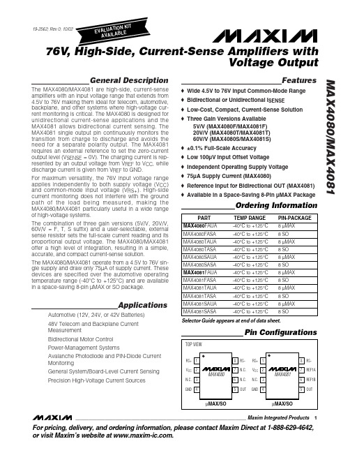
Operating Temperature Range .........................-40°C to +125°C Junction Temperature ......................................................+150°C Storage Temperature Range .............................-65°C to +150°C Lead Temperature (soldering, 10s) .................................+300°C
RS+ 1 VCC 2 N.C. 3 GND 4
MAX4080
8 RS- RS+ 1 7 N.C. VCC 2 6 N.C. N.C. 3 5 OUT GND 4
MAX4081
8 RS7 REF1A 6 REF1B 5 OUT
μMAX/SO
国内外压敏电阻型号及参数

国内外压敏电阻型号及参数压敏电阻220V电压的电路国内型号:MYG14K471(对应的国外型号:US 470NR-14D)MYG05K471(对应的国外型号:US 470NR-5D)22V左右的电路国内型号:MYG14K470(对应的国外型号:US 470NR-14D)MYG05K470(对应的国外型号:US 470NR-5D)。
压敏电阻型号及参数压敏电阻压敏电阻“压敏电阻"是中国大陆的名词,意思是在一定电流电压范围内电阻值随电压而变,或者是说"电阻值对电压敏感"的阻器。
英文名称叫“Voltage Dependent Resistor”简写为“VDR”, 或者叫做“Varistor"。
压敏电阻器的电阻体材料是半导体,所以它是半导体电阻器的一个品种。
现在大量使用的"氧化锌"(ZnO)压敏电阻器,它的主体材料有二价元素(Zn)和六价元素氧(O)所构成。
所以从材料的角度来看,氧化锌压敏电阻器是一种“Ⅱ-Ⅵ族氧化物半导体”。
在中国台湾,压敏电阻器称为"突波吸收器",有时也称为“电冲击(浪涌)抑制器(吸收器)”。
目录[]1、压敏电阻电路的“安全阀”作用2、压敏电阻的应用类型3、保护用压敏电阻的基本性能4. 压敏电阻的基本参数1、压敏电阻电路的“安全阀”作用2、压敏电阻的应用类型3、保护用压敏电阻的基本性能4. 压敏电阻的基本参数1、压敏电阻电路的“安全阀”作用压敏电阻有什么用?压敏电阻的最大特点是当加在它上面的电压低于它的阀值" UN"时,流过它的电流极小,相当于一只关死的阀门,当电压超过UN时,流过它的电流激增,相当于阀门打开。
利用这一功能,可以抑制电路中经常出现的异常过电压,保护电路免受过电压的损害。
2、压敏电阻的应用类型不同的使用场合,应用压敏电阻的目的,作用在压敏电阻上的电压/电流应力并不相同,因而对压敏电阻的要求也不相同,注意区分这种差异,对于正确使用是十分重要的。
MT40A1G8SA-075_E
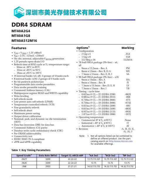
DDR4 SDRAM MT40A2G4MT40A1G8MT40A512M16Features•V DD = V DDQ = 1.2V ±60mV•V PP = 2.5V, –125mV, +250mV•On-die, internal, adjustable V REFDQ generation •1.2V pseudo open-drain I/O•Refresh time of 8192-cycle at T C temperature range:–64ms at -40°C to 85°C–32ms at >85°C to 95°C–16ms at >95°C to 105°C•16 internal banks (x4, x8): 4 groups of 4 banks each •8 internal banks (x16): 2 groups of 4 banks each •8n-bit prefetch architecture•Programmable data strobe preambles•Data strobe preamble training•Command/Address latency (CAL)•Multipurpose register READ and WRITE capability •Write leveling•Self refresh mode•Low-power auto self refresh (LPASR)•Temperature controlled refresh (TCR)•Fine granularity refresh•Self refresh abort•Maximum power saving•Output driver calibration•Nominal, park, and dynamic on-die termination (ODT)•Data bus inversion (DBI) for data bus •Command/Address (CA) parity•Databus write cyclic redundancy check (CRC)•Per-DRAM addressability•Connectivity test•JEDEC JESD-79-4 compliant•sPPR and hPPR capability Options1Marking •Configuration– 2 Gig x 42G4– 1 Gig x 81G8–512 Meg x 16512M16•78-ball FBGA package (Pb-free) – x4,x8–9mm x 13.2mm – Rev. A PM–8mm x 12mm – Rev. B, D, G WE–7.5mm x 11mm – Rev. E, H, J SA •96-ball FBGA package (Pb-free) – x16–9mm x 14mm – Rev. A HA–8mm x 14mm – Rev. B JY–7.5mm x 13.5mm – Rev. D, E, H LY–7.5mm x 13mm – Rev. J TB •Timing – cycle time–0.625ns @ CL = 22 (DDR4-3200)-062E–0.682ns @ CL = 21 (DDR4-2933)-068–0.750ns @ CL = 19 (DDR4-2666)-075–0.750ns @ CL = 18 (DDR4-2666)-075E–0.833ns @ CL = 17 (DDR4-2400)-083–0.833ns @ CL = 16 (DDR4-2400)-083E–0.937ns @ CL = 15 (DDR4-2133)-093E– 1.071ns @ CL = 13 (DDR4-1866)-107E •Operating temperature–Commercial (0° ื T Cื 95°C)None–Industrial (–40° ื T Cื 95°C)IT–Automotive (–40° ื T Cื 105°C)AT •Revision:A, :B, :D, :E,:G, :H, :J Note: 1.Not all options listed can be combined todefine an offered product. Use the partcatalog search on for available offerings.Table 1: Key Timing ParametersFunctional DescriptionThe DDR4 SDRAM is a high-speed dynamic random-access memory internally config-ured as sixteen banks (4 bank groups with 4 banks for each bank group) for x4/x8 devi-ces, and as eight banks for each bank group (2 bank groups with 4 banks each) for x16devices. The device uses double data rate (DDR) architecture to achieve high-speed op-eration. DDR4 architecture is essentially an 8n -prefetch architecture with an interface designed to transfer two data words per clock cycle at the I/O pins. A single read or write access for a device module effectively consists of a single 8n -bit-wide, four-clock-cycle-data transfer at the internal DRAM core and eight corresponding n -bit-wide, one-half-clock-cycle data transfers at the I/O pins.Read and write accesses to the device are burst-oriented. Accesses start at a selected lo-cation and continue for a burst length of eight or a chopped burst of four in a program-med sequence. Operation begins with the registration of an ACTIVE command, which is then followed by a READ or WRITE command. The address bits registered coincident with the ACTIVE command are used to select the bank and row to be accessed (BG[1:0]select the bank group for x4/x8, and BG0 selects the bank group for x16; BA[1:0] select the bank, and A[17:0] select the row. See the Addressing section for more details). The address bits registered coincident with the READ or WRITE command are used to select the starting column location for the burst operation, determine if the auto PRECHARGE command is to be issued (via A10), and select BC4 or BL8 mode on-the-fly (OTF) (via A12) if enabled in the mode register.Prior to normal operation, the device must be powered up and initialized in a prede-fined manner. The following sections provide detailed information covering device reset and initialization, register definition, command descriptions, and device operation.NOTE: The use of the NOP command is allowed only when exiting maximum power saving mode or when entering gear-down mode.8Gb: x4, x8, x16 DDR4 SDRAMFunctional Description质量等级领域:宇航级IC 、特军级IC 、超军级IC 、普军级IC 、禁运IC 、工业级IC,军级二三极管,功率管等;应用领域:航空航天、船舶、汽车电子、军用计算机、铁路、医疗电子、通信网络、电力工业以及大型工业设备祝您:工作顺利,生活愉快!以深圳市美光存储技术有限公司提供的参数为例,以下为MT40A1G8SA-075_E的详细参数,仅供参考Maximum power savings mode , Per-DRAM addressability mode, and CA parity latency modeThe mode register contents can be changed using the same command and timing re-quirements during normal operation as long as the device is in idle state; that is, all banks are in the precharged state with t RP satisfied, all data bursts are completed, and CKE is HIGH prior to writing into the mode register. If the R TT(NOM) feature is enabled in the mode register prior to and/or after an MRS command, the ODT signal must contin-uously be registered LOW, ensuring R TT is in an off state prior to the MRS command. The ODT signal may be registered HIGH after t MOD has expired. If the R TT(NOM) feature is disabled in the mode register prior to and after an MRS command, the ODT signal can be registered either LOW or HIGH before, during, and after the MRS command. The mode registers are divided into various fields depending on functionality and modes.In some mode register setting cases, function updating takes longer than t MOD. This type of MRS does not apply t MOD timing to the next valid command, excluding DES. These MRS command input cases have unique MR setting procedures, so refer to indi-vidual function descriptions.Mode Register 0Mode register 0 (MR0) controls various device operating modes as shown in the follow-ing register definition table. Not all settings listed may be available on a die; only set-tings required for speed bin support are available. MR0 is written by issuing the MRScommand while controlling the states of the BG x, BA x, and A x address pins. The map-ping of address pins during the MRS command is shown in the following MR0 RegisterDefinition table.Table 7: MR0 Register Definition (Continued)Notes: 1.Not allowed when 1/4 rate gear-down mode is enabled.2.If WR requirement exceeds 28 clocks or RTP exceeds 14 clocks, WR should be set to 28clocks and RTP should be set to 14 clocks.Burst Length, Type, and OrderAccesses within a given burst may be programmed to sequential or interleaved order.The ordering of accesses within a burst is determined by the burst length, burst type,。
石油化工用过滤器.doc
过滤器是除掉流体中固体杂质的设备,用以保护主要设备的正常运转。
一般设置在润滑油进入设备之前;燃料油进入喷嘴之前;原料油或封油进入泵之前,蒸汽凝结水进入疏水阀之前的各类管道上。
过滤器按使用要求可分为永久性过滤器和临时过滤器两种:临时过滤器仅在开工试运时使用,永久过滤器则作为一个工艺设备投入正常运转,连续生产过程中使用的永久性过滤器一般需采用两台并联安装,以便切换清洗。
由于过滤器设计时,均按接管尺寸考虑了相应的过滤面积,一般可直接根据工艺管径选用,当常用的过滤器面积不能满足工艺要求时,可更换滤网规格或选用加长型过滤器,滤网规格并在料表中注明。
过滤器壳体材料有碳钢、合金钢和不锈钢等,应根据工艺条件选定。
过滤器内件滤筒和滤网一般用不锈钢材料制作,如果工艺过程有特殊要求时,应专门注明过滤器内件材质。
───────立式过滤器(永久性)────────1、BB 型过滤器网状过滤器设计压力为1~4Mpa ,设计温度为200℃,滤网由两层组成:内层为¢2.2No5钢丝网,外层为16目/英寸的铜丝网。
工业金属丝编织方孔筛网结构参数BB 型过滤器网状过滤器外形尺寸注:1、PN≤2.5Mpa 为光滑面平焊法兰(JB-81-59),PN=4Mpa 为凹面对焊法兰(JBB-82-59) 2、标记示例:选BB 型,公称压力为1.6Mpa ,接管直径200mm ,其型号标记为BB1200-1.62、BF 型过滤器BF 型过滤器分为直通式、高低接管式和重叠式三种,过滤器的接管法兰的标准以国家标准(GB )为基础,也可以采用化工部、一机部或其他国内外标准制造,无论用那种法兰标准,滤器的安装尺寸均用下面各表中所列数值。
BF 型过滤器的标记为:①②③-④⑤ ①过滤器类型:直通蓝式:BF 平板结构 BFA 封头结构;高低接管篮式:BFAG 平板结构;BFAB 封头结构; 高低接管重叠篮式:BFAC ②公称压力 ③材质④接管公称直径: ⑤接管法兰密封面公称压力材质法兰密封面BF-系列篮式过滤器的标记为:(1)直通篮式过滤器BF型过滤器如图所示,其安装尺寸见表BF型过滤器BF型过滤器安装尺寸注:1、括弧内的数字为BF型的重量2、BF型的公称压力为PN1.6、2.5、4.0(Mpa0)BF型公称压力为PN2.0、5.0(Mpa)⑵直通篮式过滤器BFA型过滤器如图所示,其安装尺寸见表BFA型过滤器BFA型过滤器安装尺寸注:1、括弧内数字为BFA的质量;2、BFA型公称压力:PN1.62.54.0(Mpa);BFA型公称压力为PN2.05.0(Mpa)。
