GRM1555C1H471JA01D中文资料
国内外压敏电阻型号及参数
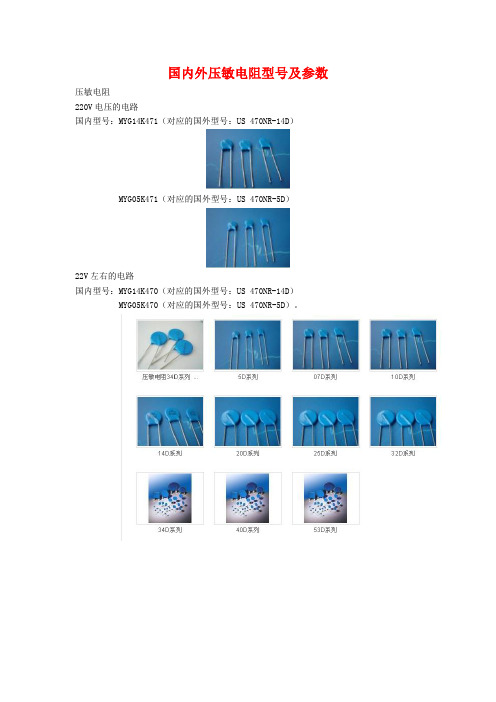
国内外压敏电阻型号及参数压敏电阻220V电压的电路国内型号:MYG14K471(对应的国外型号:US 470NR-14D)MYG05K471(对应的国外型号:US 470NR-5D)22V左右的电路国内型号:MYG14K470(对应的国外型号:US 470NR-14D)MYG05K470(对应的国外型号:US 470NR-5D)。
压敏电阻型号及参数压敏电阻百科名片压敏电阻“压敏电阻"是中国大陆的名词,意思是在一定电流电压范围内电阻值随电压而变,或者是说"电阻值对电压敏感"的阻器。
英文名称叫“Voltage Dependent Resistor”简写为“VDR”,或者叫做“Varistor"。
压敏电阻器的电阻体材料是半导体,所以它是半导体电阻器的一个品种。
现在大量使用的"氧化锌"(ZnO)压敏电阻器,它的主体材料有二价元素(Zn)和六价元素氧(O)所构成。
所以从材料的角度来看,氧化锌压敏电阻器是一种“Ⅱ-Ⅵ族氧化物半导体”。
在中国台湾,压敏电阻器称为"突波吸收器",有时也称为“电冲击(浪涌)抑制器(吸收器)”。
目录[隐藏]1、压敏电阻电路的“安全阀”作用2、压敏电阻的应用类型3、保护用压敏电阻的基本性能4. 压敏电阻的基本参数1、压敏电阻电路的“安全阀”作用2、压敏电阻的应用类型3、保护用压敏电阻的基本性能4. 压敏电阻的基本参数[编辑本段]1、压敏电阻电路的“安全阀”作用压敏电阻有什么用?压敏电阻的最大特点是当加在它上面的电压低于它的阀值" UN"时,流过它的电流极小,相当于一只关死的阀门,当电压超过UN时,流过它的电流激增,相当于阀门打开。
利用这一功能,可以抑制电路中经常出现的异常过电压,保护电路免受过电压的损害。
[编辑本段]2、压敏电阻的应用类型不同的使用场合,应用压敏电阻的目的,作用在压敏电阻上的电压/电流应力并不相同,因而对压敏电阻的要求也不相同,注意区分这种差异,对于正确使用是十分重要的。
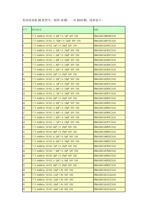
常用电容电感值
73
日本muRata C0402,68nF±10% 16V X7R
GRM155R71C683KA88D
74
日本muRata C0402,82nF±10% 16V X7R
GRM155R71C823KA88D
75
日本muRata C0402,100nF±10% 16V X7R
GRM1555C1H8R2DZ01D
28
日本muRata C0402,9pF±0.25pF 50V C0G
GRM1555C1H9R0CZ01D
29
日本muRata C0402,10pF±5% 50V C0G
GRM1555C1H100JZ01D
30
日本muRata C0402,11pF±5% 50V C0G
GRM155R71H821KA01D
61
日本muRata C0402,1nF±10% 50V X7R
GRM155R71H102KA01D
62
日本muRata C0402,1.5nF±5% 50V X7R
GRM155R71H152JA01D
63
日本muRata C0402,2.2nF±10% 50V X7R
GRM1555C1H110JA01D
31
日本muRata C0402,12pF±5% 50V C0G
GRM1555C1H120JZ01D
32
日本muRata C0402,15pF±5% 50V C0G
GRM1555C1H150JZ01D
33
日本muRata C0402,16pF±5% 50V C0G
GRM1555C1H4R3CZ01D
19
日本muRata C0402,4.7pF±0.25pF 50V C0G
手机成本( 英飞凌+安凯)
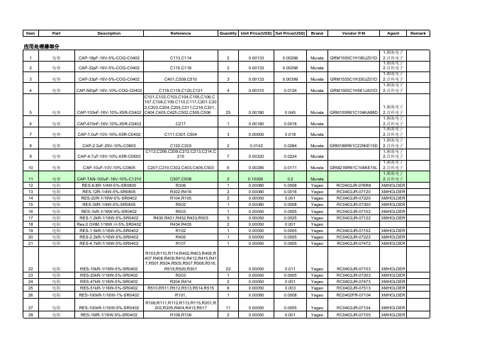
Item Part Description Reference Quantity Unit Price(USD)Set Price(USD)Brand Vendor P/N Agent Remark1电容CAP-18pF-16V-5%-COG-C0402C113,C11420.001330.00266Murata GRM1555C1H180JZ01D 1.湘海电子2.首科电子2电容CAP-32pF-16V-5%-COG-C0402C115,C11620.001330.00266Murata 1.湘海电子2.首科电子3电容CAP-33pF-16V-5%-COG-C0402C401,C509,C51030.001330.00399Murata GRM1555C1H330JZ01D 1.湘海电子2.首科电子4电容CAP-560pF-16V-10%-COG-C0402C118,C119,C120,C12140.003100.0124Murata GRM1555C1H561JA01D 1.湘海电子2.首科电子5电容CAP-100nF-16V-10%-X5R-C0402C101,C102,C103,C104,C105,C106,C107,C108,C109,C110,C117,C201,C202,C203,C204,C205,C211,C216,C301,C404,C405,C425,C502,C505,C506250.001800.045Murata GRM155R61C104KA88D1.湘海电子2.首科电子6电容CAP-470nF-16V-10%-X5R-C0402C21710.001800.0018Murata 1.湘海电子2.首科电子7电容CAP-1.0uF-10V-10%-X5R-C0402C111,C501,C50430.006000.018Murata 1.湘海电子2.首科电子8电容CAP-2.2uF-25V-10%-C0603C122,C30320.01420.0284Murata GRM188R61C225KE15D 1.湘海电子2.首科电子9电容CAP-4.7uF-16V-10%-X5R-C0603C112,C206,C209,C212,C213,C214,C21570.003200.0224Murata1.湘海电子2.首科电子10电容CAP-10uF-10V-10%-C0805C207,C210,C302,C403,C406,C50360.002850.0171Murata GRM21BR61C106KE15L 1.湘海电子2.首科电子11电容CAP-TAN-100uF-16V-10%-C1210C507,C50820.100000.2Murata 1.湘海电子2.首科电子12电阻RES-6.8R-1/4W-5%-SR0805R30610.000800.0008Yageo RC0402JR-076R8XMHOLDER 13电阻RES-12R-1/4W-5%-SR0805R302,R41620.000800.0016Yageo RC0402JR-07120XMHOLDER 14电阻RES-22R-1/16W-5%-SR0402R104,R10520.000500.001Yageo RC0402JR-07220XMHOLDER 15电阻RES-30R-1/4W-5%-SR0805R50210.000800.0008Yageo RC0402JR-07300XMHOLDER 16电阻RES-1kR-1/16W-5%-SR0402R50310.000500.0005Yageo RC0402JR-07102XMHOLDER 17电阻RES-1.2kR-1/16W-5%-SR0402R430,R431,R432,R433,R50350.000500.0025Yageo RC0402JR-07122XMHOLDER 18电阻Res,0 OHM,1/16W,+/-5%,SR0402R434,R43520.000500.001Yageo19电阻RES-1.5kR-1/16W-5%-SR0402R10210.000500.0005Yageo RC0402JR-07152XMHOLDER 20电阻RES-2.2kR-1/16W-5%-SR0402R40510.000500.0005Yageo RC0402JR-07222XMHOLDER 21电阻RES-4.7kR-1/16W-5%-SR0402R10710.000500.0005Yageo RC0402JR-07472XMHOLDER22电阻RES-10kR-1/16W-5%-SR0402R103,R110,R114,R402,R403,R406,R407,R408,R409,R410,R412,R415,R417,R501,R504,R505,R507,R508,R516,R519,R520,R301220.000500.011Yageo RC0402JR-07103XMHOLDER23电阻RES-20kR-1/16W-5%-SR0402R20310.000500.0005Yageo RC0402JR-07203XMHOLDER 24电阻RES-47kR-1/16W-5%-SR0402R204,R41420.000500.001Yageo RC0402JR-07473XMHOLDER 25电阻RES-51kR-1/16W-5%-SR0402R510,R511,R512,R513,R514,R51560.000500.003Yageo RC0402JR-07513XMHOLDER 26电阻RES-100kR-1/16W-1%-SR0402R101,10.000800.0008Yageo RC0402FR-07104XMHOLDER27电阻RES-100kR-1/16W-5%-SR0402R106,R111,R112,R113,R115,R201,R202,R205,R404,R413,R517110.000500.0055Yageo RC0402JR-07104XMHOLDER28电阻RES-1MR-1/16W-5%-SR0402R108,R10920.000500.001Yageo RC0402JR-07105XMHOLDER 应用处理器部分29磁珠BLM-75R-25%-300mA-0402L101,L102,L40130.00350.0105Murata BLM15BB750SN11.湘海电子2.首科电子30功率电感IND-3.3uH-10%-1210L20110.0450000.045顺络电子顺络电子31功率电感IND-22uH-10%-1210L30210.0450000.045顺络电子顺络电子32滤波器EXC24CD121FL40110.1083400.1083panasonic33磁珠BLM-600R-25%-100mA-0402B301,B50120.0063030.012606panasonic EXC3BB601H京凌科技34NPN型三极管TRAN-NPN-40V-200mA-SOT23Q401,Q50120.0300000.06Philips PMBT3904,sot23安富利35N沟道增强型MOS管TRAN-MOS-N-60V-TO-236AB Q40210.0300000.03Philips2N7002,sot23安富利36ESD 保护(压敏电阻)RES-VAR-20%-5.5V-0402RD101,D102,D202,D313,D410,D411,D412,D413,D414,D415,D416,D510,D511,D512140.0005000.007Epcos CT0402M4G俊成科技37ESD保护器件RES-6.4Vto7.2V-45pF-SOT23D103,D401,D402,D403,D503,D504,D505,D506,D50790.0340000.306Toshiba DF5A6.8FU台和38二极管DIO-30V-1A-SOD-523/SC-79D201,D412,D418,D50240.0143000.0572Rohm1SS4001.研达科技2.科发电子39肖特基二极管DIO-SCHO-20V-500mA-SOD-123D31710.0143000.0143Diodes B0530WS40键盘灯LED-BLUE-0603-5mA D419,D420,D421,D422,D423,D42460.03000.18佰鸿蓝光LED億威利41SD卡座,CON-SD-Amphenol JS50110.4000000.4Amphenol GSD11001AEU睿吉通电子42触摸屏连接器CON-4pin-0.5SH J10110.0900000.0900Hiros FH19-4S-0.5SH(48)1.信邦电子2.兆崴国际43电池连接器CON-Battery-3pin-2.5PH-4.3H J20110.1000000.1创丰电子BC-3P-2.5PH-4.3H创丰电子44LCD连接器CON-LCD-Nais J30110.2200000.22Nais AXK7L30227G 1.宇科光电2.科通通信45Camera Socket CON-Camera-24pin-Mitsumi J30210.2300000.23Mitsumi R41-8558-A,(M09)1.时毅电子2.时富电子46耳机插座CON-Audio-6pin-Wieson J50110.1500000.15Wieson7272-46,Conn_6Wieson 47尾插CON-Jack-12pin J50210.2300000.23ASTRON060220ASTRON 48侧键CON-SideKey-Cityzen SW423,SW424,SW425,30.08500.255Cityzen LS10时尚科技49处理器IC-AP-AK3223-BGA244U1011 6.1000 6.1Anyka AK3223M Anyka 50反相器IC-Inverter-0.9Vto3.6V-SOT553U10210.10000.1Onsemi553安富利51SDRAM IC-SDRAM-64Mbit-3.0V-x16-TSOP U20110.88000.88Sansung K4M281633H_R(B)N/G/L/F751.AV2.三达52NANDFLASH IC-NAND-512Mb-3.0V-x8-BGA U2021 2.5000 2.5Sansung K9F1208U0B-G,L1.AV2.三达53DC-DC chip DC/DC-POW-1.8V/SOT23-5U20310.35000.35Torex XC9216A18CMRN长天电子54LDO LDO-POW-3V-300mA-SOT-23U20410.25000.25Micrel MIC5259-3.0BD51.世强电讯2.艾睿电子55LDO,3.3V LDO-POW-3.3V-300mA-SOT-23U20510.25000.25Micrel MIC5259-3.3BD51.世强电讯2.艾睿电子56LDO POW-LDO-2.5V-150mA-SOT25U20610.07500.075Torex XC6209A252MR /SOT25长天电子57LCD背光升压芯片POW-DC/DC-2.5Vto6V-SOT23-6U30210.20000.2MPS MP1518TBD58缓冲器IC-Buffer-1.65Vto5.5V-24mA/3V-2.6ns/50pF,5V-MicroPAK U401,U40220.10000.2Fairchild NC7SZ1251.Fairchild2.安富利59晶振CRY-26MHz-10pF-±30ppm-SMD Y10110.20000.2TAITIEN XVCGGCNANF-26MHZ,TAITIEN60晶振CRY-32.768kHz-20pF-±30ppm-SMD Y10210.15000.15Epson MC1461.中电2.众文远达18714.1928561电容CAP-1pF-16V-10%-C0402C70310.002300.0023Murata GRM1555C1H1R0BZ01D 1.湘海电子2.首科电子2电容CAP-1.2pF-16V-10%-C0402C71310.002300.0023Murata GRM1555C1H1R2BZ01D 1.湘海电子2.首科电子3电容CAP-1.8pF-16V-10%-C0402C718,C72220.002800.0056Murata GRM1555C1H1R8BZ01D 1.湘海电子2.首科电子4电容CAP-4.7pF-16V-10%-C0402C72410.002300.0023Murata GRM1555C1H4R7BZ01D 1.湘海电子2.首科电子5电容CAP-18pF-16V-5%-C0402C629,C63020.001330.00266Murata GRM1555C1H180JZ01D 1.湘海电子2.首科电子6电容CAP-27pF-16V-10%-C0402C643,C645,C702,C706,C707,C708,C723,C729,C730,C731,C732110.001330.01463Murata GRM1885C1H270JA01D1.湘海电子2.首科电子7电容CAP-33pF-16V-5%-C0402C631,C632,C63430.001330.00399Murata GRM1555C1H330JZ01D 1.湘海电子2.首科电子8电容CAP-4.7nF-16V-10%-C0402C704,C71720.001300.0026Murata GRM155R71H472KA01D 1.湘海电子2.首科电子9电容CAP-6.8nF-16V-10%-C0402C70110.001300.0013Murata GRM155R71H682KA88D 1.湘海电子2.首科电子10电容CAP-47nF-16V-10%-C0402C601,C705,C70930.002700.0081Murata GRM155R71C473KA01D 1.湘海电子2.首科电子11电容CAP-68nF-16V-10%-C0402C61010.003300.0033Murata GRM155R71C683KA88D 1.湘海电子2.首科电子12电容CAP-100nF-16V-10%-C0402C605,C608,C609,C619,C620,C621,C622,C623,C627,C628,C633,C637,C638,C639,C640,C712160.001580.02528Murata GRM155R71C104KA88D1.湘海电子2.首科电子13电容CAP-2.2uF-16V-10%-C0402C604,C606,C611,C612,C613,C614,C615,C616,C617,C624,C625,C626120.003200.0384Murata1.湘海电子2.首科电子14电容CAP-10uF-16V-10%-C0805C635,C636,C64430.029000.087Murata GRM21BR61C106KE15L 1.湘海电子2.首科电子15电容CAP-22uF-6.3V-20%-TC1210C602,C60720.070000.14Murata GRM31CR60J226ME19L 1.湘海电子2.首科电子16电容CAP-TAN-100uF-6.3V-20%-TC1210C60310.100000.1Murata1.湘海电子2.首科电子17电容CAP-TAN-150uF-6.3V-20%-TC1210C61810.100000.1Murata1.湘海电子2.首科电子18电阻RES-0R-1/16W-5%-SR0402R605,R606,R608,R620,R702,R704,R705,R70670.000500.0035Yageo RC0402JR-070XMHOLDER19电阻RES-0.15R-1/16W-5%-SR0402R60110.030000.03Yageo RC0402JR-070R15XMHOLDER 20电阻RES-4.7R-1/16W-5%-SR0402R60710.000500.0005Yageo RC0402JR-074R7XMHOLDER 21电阻RES-22R-1/16W-5%-SR0402R625,R626,R62730.000500.0015Yageo RC0402JR-07220XMHOLDER 22电阻RES-220R-1/16W-5%-SR0402R701,10.000500.0005Yageo RC0402JR-07221XMHOLDER 23电阻RES-1kR-1/16W-5%-SR0402R703,10.000500.0005Yageo RC0402JR-07102XMHOLDER 24电阻RES-1.5kR-1/16W-5%-SR0402R61810.000500.0005Yageo RC0402JR-07152XMHOLDER 25电阻RES-2.2kR-1/16W-5%-SR0402R62110.000500.0005Yageo RC0402JR-07222XMHOLDER 26电阻RES-4.7kR-1/16W-5%-SR0402R61510.000500.0005Yageo RC0402JR-07472XMHOLDER 27电阻RES-10kR-1/16W-5%-SR0402R61110.000500.0005Yageo RC0402JR-07103XMHOLDER 28电阻RES-22kR-1/16W-5%-SR0402R602,R612,R613,R62240.000500.002Yageo RC0402JR-07223XMHOLDER 29电阻RES-47kR-1/16W-5%-SR0402R61410.000500.0005Yageo RC0402JR-07473XMHOLDER 30电阻RES-82kR-1/16W-5%-SR0402R60910.000810.00081Yageo RC0402JR-07823XMHOLDER 基带射频部分31电阻RES-100kR-1/16W-5%-SR0402R617,R62420.000500.001Yageo RC0402JR-07104XMHOLDER 32电阻RES-220kR-1/16W-5%-SR0402R604,R62320.000500.001Yageo RC0402JR-07224XMHOLDER 33电阻RES-390kR-1/16W-5%-SR0402R61610.000500.0005Yageo RC0402JR-07394XMHOLDER 34电阻RES-560kR-1/16W-5%-SR0402R60310.000500.0005Yageo RC0402JR-07564XMHOLDER 35电阻RES-1MR-1/16W-5%-SR0402R61010.000500.0005Yageo RC0402JR-07105XMHOLDER 36电感IND-1.5nH-10%-0402L70710.00500.005顺络电子顺络电子37电感IND-2.2nH-10%-0402L704,L70520.00500.01顺络电子顺络电子38电感IND-6.2nH-20%-0402-Wirewound L71110.04500.045顺络电子顺络电子39电感IND-15nH-3%-0402-Wirewound L709,L71020.04500.09顺络电子顺络电子40电感IND-10uH-10%-1210L601,L60220.03500.07顺络电子顺络电子41电感BLM15BB750SN1L629,L63020.00350.007Murata42二极管DIO-SCHO-10V-3A-SOD-323D60110.02900.029Infineon BAT60B,品佳电子43ESD保护器件RES-VAR-20%-5.5V-0402R D602,D60320.00050.001Toshiba ESD,CT0402M4G台和44mos管TRAN-MOSFET-P-2.5V-TSOP6Q60110.1050.105Infineon BSL211SP品佳电子45mos管TRAN-MOSFET-P-2.5V-SOT323Q60210.04680.0468Infineon BSS223PW品佳电子46复合管TRAN-PNP/NPN-SOT363Q60310.2160.216Infineon BCR39PN品佳电子47SIM卡座CON-simcard-0.9H JR60110.12000.12linktek SIMSH-00630-TP00良泽电子48射频连接头CON-RF-Murata J70110.11000.11Murata CRS5001-1003_1,MM8430A湘海电子49声表滤波器SAW-Impedance50Ω(I)/150Ω(O)-925to960MHz/InsertionLoss2.7Db/VSWR2.0/RippleDeviation1.8dB/AmplitudeBalance±1.0dB/PhaseBalance180±10°BP70210.15000.15EPCOS B78371.EPCOS2.俊成科技50声表滤波器SAW-Impedance50Ω(I)/150Ω(O)-1805to1880MHz/InsertionLoss2.5dB/VSWR2.2/RippleDeviation1.5dB/AmplitudeBalance±1.5dB/PhaseBalance180±12°BP70310.17000.17EPCOS B78521.EPCOS2.俊成科技51电源管理芯片PMU-PMB6814-VQFN48-Infineon U6011 1.2 1.2Infineon PMB6814品佳电子52存储器IC-FLA-2.7Vto3.1V-32MbNor-8MbpSRAM-56pin FBGA U6021 2.5000 2.5Spansion S71GL032A801.时尚科技2.威健实业53基带/射频处理器BB/RF-PMB7870-LFBGA233-Infineon U6031 4.8 4.8Infineon PMB7870品佳电子54天线开关Switch-ANT-12pin-TDK U70110.58000.58TDK ASM4518807T-250355射频PAPA-2BAND-GSM850(824to849MHz)/GSM900(880to915MHz)/DSC(1710to1785MHz)/ PSC(1850to1910MHz)-GSM35dB/3.5V-DCS/PCS33dB/3.5V-LFM48P U7021 1.3000 1.3RFMD RF31661.光明电子2.世健56晶振p ppSMD Y60110.15000.15MC MS2V-T1S普荣实业57晶振CRY-26MHz-10pF-±10ppm-SMD Y70110.34000.34Kyocera CX3225YB26000F0FLFZZ普荣实业12112.62987PCB 1.5PCBA28.3227261喇叭直径20mm ,弹片式LS10110.50000.5000Keyrin 2咪头MK40110.25000.2500BSE 3马达弹片胶套电机MOTOR50110.43000.4300韩国永柏4受话器32ohm Receiver LS60110.12000.1200Keyrin 5LCD LCD-2.2''-320x240-MPU 112.000012.0000Truly 6摄像头CAM-1.3M-CMOS 1 5.9000 5.9000Sunny7外壳结构件1 2.2000 2.20008电池1 1.2000 1.20009充电器1 1.0000 1.000010数据线10.80000.800011光盘10.15000.150012耳机10.80000.800013包装件10.50000.500025.850054.17271闪光灯驱动U30110.4800000.4800002闪光灯D31110.3800000.380000装配件与周转件可选件整机BOM 20-8E-09Keyrin OBG415L44C1033R宝星电子YB43DD-1麒麟通讯KR -1406C -01PKeyrin Truly 8108H 邦 泽 科 技LM2753SDCL-690S-2WF ,Flash Led。
ISL85005和ISL85005A演示板用户指南说明书
ISL85005ADEMO1Z ISL85005DEMO1ZISL85005DEMO1Z and ISL85005ADEMO1Z Demonstration Boards User GuideDescriptionThe ISL85005 and ISL85005A are 4.5V to 18V input, 5A synchronous buck regulators for applications with input voltage from multi-cell batteries or regulated 5V and 12Vpower rails. These devices also provide an integrated bootstrap diode for the high-side gate driver to reduce the external parts count. The ISL85005DEMO1Z and ISL85005ADEMO1Zplatforms allow quick demonstration of the high performance features of the ISL85005 and ISL85005A buck regulators.SpecificationsThese boards have been configured and optimized for the following operating conditions: •Input voltage ranges from 7V to 15V •5V nominal output voltage •Up to 5A output current capability•Default internally set 500kHz switching frequency •Default internally set 2.3ms soft-start•Operating temperature range: -40°C to +85°CKey Features•Switch selectable EN (enabled/disabled)•Selectable mode (DEM/Forced CCM) (ISL85005DEMO1Z)•Internal and external compensation options•Frequency synchronization option (ISL85005DEMO1Z)•Adjustable soft-start option (ISL85005ADEMO1Z)•Small and compact designRelated Literature•For a full list of related documents please visit our website -ISL85005 and ISL85005A product pagesOrdering InformationPART NUMBER DESCRIPTIONISL85005DEMO1Z Small form-factor demonstration board for ISL85005FRZISL85005ADEMO1ZSmall form-factor demonstration board for ISL85005AFRZFIGURE 1A.ISL85005DEMO1ZFIGURE 1B.ISL85005ADEMO1ZFIGURE 1.BLOCK DIAGRAMSYNC/PG EN FB COMP BOOT VDD VIN VIN PHASE AGND234151*********PHASE PGNDC 3C 4C 5C 6C 8C 9MODE GND = DEM; VCC = FCCM EN PG MODE V INL 1V OUTISL85005R 2C 1R 1PGENFB COMP BOOT VDD VIN VIN PHASE AGND234151110912867PHASE PGNDC 3C 4C 5C 6C 8C 9EN PG V INL 1V OUTISL85005AR 2C 1R 1SS C SSUser Guide 110User Guide 110Connector and Selection Jumper DescriptionsThe ISL85005DEMO1Z and ISL85005ADEMO1Z demonstration boards include I/O connectors and a selection jumper as shown in Table1.Quick Setup GuideRefer to the following Quick Setup Guide to configure and power-up the board for proper operation.1.Set the power supply voltage to 12V, and turn off the powersupply. Connect the positive output of power supply to J3 (VIN) and the negative output to J4 (GND).2.Connect an electronic load to J5 (VOUT) for the positiveconnection and J6 (GND) for the negative connection.3.Measure the output voltage (J5 and J6) with the voltmeter.4.Place scope probes on VOUT and other test points of interest.5.Set EN jumper (J1) to ON position.6.Set the load current to be 0.1A and turn on the power supply,the output voltage should be in regulation with a nominal 5V output.7.Slowly increase the load up to 5A while monitoring the outputvoltage which should remain in regulation with a nominal 5V output.8.Slowly sweep VIN from 7V to 15V, the output voltage shouldremain in regulation with a nominal 5V output.9.Decrease the input voltage to 0V to shut down the regulator. Operation Mode Selection (ISL85005DEMO1Z)The ISL85005DEMO1Z can be configured in either forced Continuous Conduction Mode (CCM) or Diode Emulation Mode (DEM):•In the default configuration of ISL85005DEMO1Z,SYNC/MODE (Pin 1) of ISL85005 is floating, the ISL85005 operates in forced CCM.•To configure the ISL85005 in DEM, short the SYNC/MODE pin to GND by populating a 0Ω resistor for C SS. DEM enables automatic transition from CCM to DCM and higher efficiency at light-load conditions.Frequency Synchronization (ISL85005DEMO1Z)The ISL85005 can be synchronized to an external clock with frequency ranges from 300kHz to 2MHz by applying the external clock to the SYNC/MODE pin on the ISL85005DEMO1Z demonstration board. The external clock should meet the specifications of the pulse width and voltage level described in the datasheet.Adjusting Soft-Start Time(ISL85005ADEMO1Z)With the SS pin floating, the ISL85005A features an internally set 2.3ms of soft-start time. The soft-start time can be set to a desired value by connecting an external capacitor (C SS on the ISL85005ADEMO1Z demonstration board) between the SS pin and AGND. The capacitance can be calculated by Equation1:Evaluating Other Output VoltagesBoth ISL85005DEMO1Z and ISL85005ADEMO1Z have a nominal 5V output voltage. The output voltages are programmable by an external resistor divider formed by R1 and R2 as shown in Figure1 on page1. R1 is usually chosen first, then the value for R2 can be calculated based on R1 and the desired output voltage using Equation2.PCB Layout ConsiderationsThe PCB layout is critical for proper operation of the ISL85005 and ISL85005A. The following guidelines should be followed to achieve good performance.e a multilayer PCB structure to achieve optimizedperformance, a four-layer PCB is recommended for thisdesign.e a combination of bulk capacitors and smaller ceramiccapacitors with lower ESL for the input capacitors and place them as close to the IC as possible.3.Place the VDD decoupling capacitor close to the IC betweenVDD and GND. A 1µF ceramic capacitor is typically used. 4.Place a bootstrap capacitor close to the IC between the BOOTand PHASE pins. A 0.1µF ceramic capacitor is typically used.5.Connect the feedback resistor divider between the outputcapacitor positive terminal and the AGND pin of the IC, and place the resistors close to the FB pin of the IC.6.Connect the EPAD of the IC to the GND planes underneathusing multiple thermal vias to improve thermal performance.TABLE 1.CONNECTORS AND JUMPERREFERENCEDESIGNATOR DESCRIPTIONJ1Selection Jumper for Enable (EN)J3Input voltage positive connectionJ4Input voltage return connectionJ5Output voltage positive connectionJ6Output voltage return connectionC SS nF[] 3.5t SS ms[] 1.6nF–⋅=(EQ. 1)R2R10.8V⋅V OUT0.8V–----------------------------------=(EQ. 2)User Guide 110 ISL85005xDEMO1Z Demonstration BoardFIGURE 2.TOP VIEW SchematicFIGURE 3.ISL85005xDEMO1Z SCHEMATICUser Guide 110 Bill of MaterialsMANUFACTURER PART NUMBER REFERENCEDESIGNATOR QTY DESCRIPTION MANUFACTURERISL85005FRZ(ISL85005DEMO1Z)U11IC-BUCK REGULATOR W/ SYNC/MODE PIN, 12PIN, DFN, 3x4, ROHS INTERSILISL85005AFRZ(ISL85005ADEMO1Z)1IC-BUCK REGULATOR W/ SS PIN, 12PIN, DFN, 3x4, ROHS INTERSILGRM1555C1H120JA01D C41CAP, SMD, 0402, 12pF, 50V, 5%, NP0, ROHS MURATAC7, C8, C SS0CAP, SMD, 0402, DNP-PLACE HOLDER, ROHSGRM188R71E104KA01D C31CAP, SMD, 0603, 0.1µF, 25V, 10%, X7R, ROHS MURATAGRM188R61E105KA12D C91CAP, SMD, 0603, 1µF, 25V, 10%, X5R, ROHS MURATAC1206X7R250-106KNE C1, C22CAP, SMD, 1206, 10µF, 25V, 10%, X7R, ROHS VENKELCL32A476KOJNNNE C5, C62CAP, SMD, 1210, 47µF, 16V, 10%, X5R, ROHS SAMSUNG744314330L11COIL-PWR INDUCTOR, SMD, 6.9mm2, 3.3µH, 9A 9mΩ, WW, ROHS WURTH ELEKTRONIK 1514-2J3, J4, J5, J64CONN-TURRET, TERMINAL POST, TH, ROHS KEYSTONEERJ2RKF20R0R41RES, SMD, 0402, 20Ω, 1/16W, 1%, TF, ROHS PANASONICCR0402-16W-00T R111RES, SMD, 0402, 0Ω, 1/16W, 5%, TF, ROHS VENKELMCR01MZPF2003R7, R142RES, SMD, 0402, 200k, 1/16W, 1%, TF, ROHS ROHMCR0402-16W-4993FT R11RES, SMD, 0402, 499k, 1/16W, 1%, TF, ROHS VENKELRC0402FR-0795K3L R21RES, SMD, 0402, 95.3k, 1/16W, 1%, TF, ROHS YAGEOR3, R80RES, SMD, 0402, DNP, DNP, DNP, TF, ROHS929950-00Jumper1CONN-JUMPER, SHORTING, 2PIN, BLK, OPEN TOP, 2.54mmPITCH,ROHS3MPEC03SAAN J11 3 Positions Header, 100 mil (2.54mm) spacing, Through Hole Tin Sullins Connector Solutions ISL85005xDEMO1Z PCB1PWB-PCB, ISL85005xDEMO1Z, REVA, ROHS AnyUser Guide 110 ISL85005xDEMO1Z PCB LayoutUser Guide 110Intersil Corporation reserves the right to make changes in circuit design, software and/or specifications at any time without notice. Accordingly, the reader is cautioned to verify that the document is current before proceeding.For information regarding Intersil Corporation and its products, see Typical Performance CurvesV IN = 12V, V OUT = 5V, L = 3.3µH, f SW = 500kHz, T A = +25°C, unless otherwise noted.FIGURE 9.START-UP WITH EN, I OUT = 5AFIGURE 10.SHUTDOWN WITH EN, I OUT = 5AFIGURE 11.LOAD TRANSIENT, 0A → 2.5A → 0A, 2.5A/µsV OUT (2V/DIV)I L (2A/DIV)EN (10V/DIV)1ms/DIV200µs/DIV V OUT (2V/DIV)EN (10V/DIV)I L (2A/DIV)50µs/DIVV OUT (100mV/DIV),I OUT (1A/DIV)AC COUPLINGISL85005ADEMO1Z ISL85005DEMO1Z。
德州仪器MAX16826评估板使用手册说明书
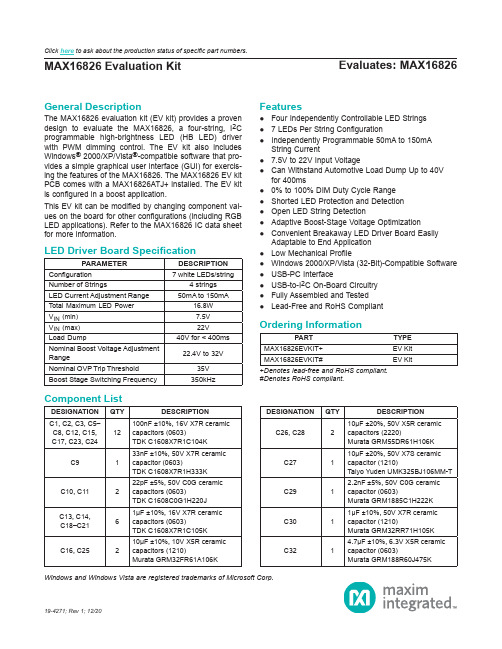
Evaluates: MAX16826MAX16826 Evaluation KitGeneral DescriptionThe MAX16826 evaluation kit (EV kit) provides a proven design to evaluate the MAX16826, a four-string, I 2C programmable high-brightness LED (HB LED) driver with PWM dimming control. The EV kit also includes Windows ® 2000/XP/Vista ®-compatible software that pro-vides a simple graphical user interface (GUI) for exercis-ing the features of the MAX16826. The MAX16826 EV kit PCB comes with a MAX16826ATJ+ installed. The EV kit is configured in a boost application.This EV kit can be modified by changing component val -ues on the board for other configurations (including RGB LED applications). Refer to the MAX16826 IC data sheet for more information.Features●Four Independently Controllable LED Strings ●7 LEDs Per String Configuration●Independently Programmable 50mA to 150mAString Current●7.5V to 22V Input Voltage●Can Withstand Automotive Load Dump Up to 40Vfor 400ms●0% to 100% DIM Duty Cycle Range ●Shorted LED Protection and Detection ●Open LED String Detection●Adaptive Boost-Stage Voltage Optimization●Convenient Breakaway LED Driver Board EasilyAdaptable to End Application ●Low Mechanical Profile●Windows 2000/XP/Vista (32-Bit)-Compatible Software ●USB-PC Interface●USB-to-I 2C On-Board Circuitry ●Fully Assembled and Tested ●Lead-Free and RoHS Compliant19-4271; Rev 1; 12/20Windows and Windows Vista are registered trademarks of Microsoft Corp.+Denotes lead-free and RoHS compliant.#Denotes RoHS compliant.PARAMETERDESCRIPTION Configuration 7 white LEDs/stringNumber of Strings4 strings LED Current Adjustment Range 50mA to 150mATotal Maximum LED Power 16.8W V IN (min)7.5V V IN (max)22V Load Dump40V for < 400ms Nominal Boost Voltage Adjustment Range22.4V to 32VNominal OVP Trip Threshold 35V Boost Stage Switching Frequency350kHzPARTTYPE MAX16826EVKIT+EV Kit MAX16826EVKIT#EV KitDESIGNATION QTY DESCRIPTIONC1, C2, C3, C5–C8, C12, C15,C17, C23, C2412100nF ±10%, 16V X7R ceramic capacitors (0603)TDK C1608X7R1C104K C9133nF ±10%, 50V X7R ceramic capacitor (0603)TDK C1608X7R1H333K C10, C11222pF ±5%, 50V C0G ceramic capacitors (0603)TDK C1608C0G1H220J C13, C14,C18–C2161μF ±10%, 16V X7R ceramic capacitors (0603)TDK C1608X7R1C105K C16, C25210μF ±10%, 10V X5R ceramic capacitors (1210)Murata GRM32FR61A106KDESIGNATION QTY DESCRIPTIONC26, C28210μF ±20%, 50V X5R ceramic capacitors (2220)Murata GRM55DR61H106K C27110μF ±20%, 50V X7S ceramic capacitor (1210)Taiyo Yuden UMK325BJ106MM-T C2912.2nF ±5%, 50V C0G ceramic capacitor (0603)Murata GRM1885C1H222K C3011μF ±10%, 50V X7R ceramic capacitor (1210)Murata GRM32RR71H105K C3214.7μF ±10%, 6.3V X5R ceramic capacitor (0603)Murata GRM188R60J475KLED Driver Board SpecificationOrdering InformationComponent ListClick here to ask about the production status of specific part numbers.DESIGNATION QTY DESCRIPTIONC3312200pF ±10%, 50V X7R ceramic capacitor (0402)Murata GRM155R71H222KC34, C35247μF ±20%, 50V electrolytic capacitorsPanasonic EEE-FK1H470XPC36, C370Not installed, capacitors (0603)C3811000pF ±5%, 50V C0G ceramic capacitor (0402)Murata GRM1555C1H102JA01DC391220pF ±5%, 50V C0G ceramic capacitor (0402)Murata GRM1555C1H221JC401100pF ±5%, 50V C0G ceramic capacitor (0402)Murata GRM1555C1H101JC41–C4440.01μF ±10%, 50V X7R ceramic capacitors (0402)Murata GRM155R71H103KC450Not installed, capacitor (0402)D1160V, 1A Schottky diode (SMB) Diodes, Inc. B160B-13-FJ11USB series-B right-angle PC-mount receptacleJ2, J30Not installed JU2–JU873-pin headersL11Ferrite bead (0603) TDK MMZ1608R301AL2122μH ±20%, 5A, 52mΩ inductor Coilcraft MSS1260-223MlLED11Red LED (0603) Panasonic LNJ208R8ARAP1, P22Connectors, FFC/FPC 18-pos, 1mm P31Connector, FFC/FPC 6-pos, 1mmQ1140V, 9A, 2.5W n-channel MOSFET (8 SO)International Rectifier IRF7469Q2–Q5455V, 1.9A, 160mΩ n-channel MOSFET s (SOT223) International Rectifier IRFL014NPbFR11220Ω ±5% resistor (0603)R21 2.2kΩ ±5% resistor (0603)R3, R9, R103 1.5kΩ ±5% resistors (0603) R4, R5227Ω ±5% resistors (0603)R61470Ω ±5% resistor (0603)R71100kΩ ±5% resistor (0603)R817.5kΩ ±1% resistor (0603)R11168Ω ±1%, 0.25W resistor (1206)DESIGNATION QTY DESCRIPTION R1210.04Ω ±1%, 0.5W sense resistor(2010)Vishay/Dale WSL2010R0400FEA R131215kΩ ±1% resistor (0402) R14, R16210kΩ ±1% resistors (0402) R151249kΩ ±1% resistor (0402)R171 1.27kΩ ±1% resistor (0603)R181182kΩ ±1% resistor (0603)R1912kΩ ±1% resistor (0402) R20, R22,R24, R264100kΩ ±1% resistors (0402) R21, R23,R25, R27416.5kΩ ±1% resistors (0402) R28–R3142.2Ω ±1%, 100mW sense resistors(0603)Panasonic ECG ERJ-3RQF2R2V R32, R3320Ω ±5% resistors (0603)R34–R3740Ω ±5% resistors (0402)R38112.1Ω ±1% resistor (0805)R391470Ω ±5% resistor (0402)R40110kΩ ±5% resistor (0603) R41–R444237kΩ ±1% resistors (0603) U11LED driver (32 TQFN)Maxim MAX16826ATJ+ U2, U82Microcontrollers (68 QFN-EP*)Maxim MAXQ2000-RAX+ U31UART-to-USB converter (32 TQFP)FTDI FT232BLU4193C46A 3-wire EEPROM (8 SO)Atmel AT93C46A-10SU-2.7 U51p-channel MOSFET power switch(8 SO)Maxim MAX890LESA+U61LDO regulator (5 SC70)Maxim MAX8511EXK25+T U71LDO regulator (5 SC70)Maxim MAX8511EXK33+T Y1120MHz crystal oscillatorY216MHz crystalHong Kong X’talsSSL6000000E18FAF—1Cable, flat flex 18-position, 1mm, 5in—7Shunts—1USB high-speed A-to-B cable,5ft (1.5m)—1PCB: MAX16828 Evaluation Kit+Component List (continued)*Exposed pad.Quick StartRecommended EquipmentBefore beginning, the following equipment is needed: ●MAX16826 EV kit (USB cable included)● A user-supplied Windows 2000/XP/Vista PC with a spare USB port●7V to 24V, 5A DC power supply●Four strings of white LEDs (7 LEDs/string)Note: In the following sections, software-related items are identified by bolding. Text in bold refers to items directly from the EV kit software. Text in bold and underlined refers to items from the Windows operating systemProcedureThe MAX16826 EV kit is fully assembled and tested. Follow the steps below to verify board operation:1) Visit /evkitsoftware to down-load the latest version of the EV kit software,16826Rxx.ZIP (xx in the filename denotes the soft -ware version number). Save the EV kit software to a temporary folder and uncompress the ZIP file.2) Install the EV kit software on your computer by run -ning the INSTALL.EXE program inside the temporary folder. The program files are copied and icons are created in the Windows Start | Programs menu.3) Verify that all jumpers (JU2–JU8) are in their defaultpositions, as shown in Table 1.4) Connect the USB cable from the PC to the EV kitboard. A New Hardware Found window pops up when installing the USB driver for the first time. If you do not see a window that is similar to the one described above after 30 seconds, remove the USB cable from the board and reconnect it. Administra-tor privileges are required to install the USB device driver on Windows.5) Follow the directions of the Add New HardwareWizard to install the USB device driver. Choose the Search for the best driver for your device option. Specify the location of the device driver to be C:\Program Files\MAX16826 (default installation direc-tory) using the Browse button. During device driver installation, Windows may show a warning message indicating that the device driver Maxim uses does not contain a digital signature. This is not an error condi-tion and it is safe to proceed with installation. Refer to the USB_Driver_Help.PDF document included with the software for additional information.6) Set the output of the power supply to 12V. Turn offthe power supply.7) Connect the positive terminal of the power supply tothe VIN pad of the LED driver board.Note: Indicate that you are using the MAX16826 when contacting these component suppliers.SUPPLIERPHONE WEBSITECoilcraft, Diodes, Inc.Hong Kong X’tals Ltd.852-******** International RectifierMurata Electronics North America, Panasonic Taiyo Yuden TDK Vishay/Dale402-563-6866FILE DESCRIPTIONINSTALL.EXE Installs the EV kit files on your computerMAX16826.EXE Application program FTDIBUS.INF USB device driver file FTDIPORT.INF VCP device driver file UNINST.INI Uninstalls the EV kit software USB_Driver_Help.PDFUSB driver installation help fileComponent SuppliersMAX16826 EV Kit Files8) Connect the negative terminal of the power supply tothe PGND pad of the LED driver board.9) Ensure that the supplied ribbon cable is firmly con -nected to the P1 and P2 connectors.10) Connect the anode ends of the LED strings to theP3-1 pin of the P3 connector.11) Connect the cathode ends of the LED strings to theP3-2 to P3-5 pins of the P3 connector.12) Turn on the power supply13) Start the MAX16826 EV kit software by opening itsicon in the Start | Programs menu. The EV kit soft-ware main window appears, as shown in Figure 1.14) Press the Start button to start the LED driver.15) Verify that all of the LEDs are lit.Table 1. MAX16826 EV Kit Jumper Descriptions (JU2–JU8)*Default position.JUMPER SHUNT POSITIONDESCRIPTIONJU21-2*On-board PWM signal for Ch12-3Connect user-supplied PWM signal for Ch1 to the on-board DIM1 pad JU31-2*On-board PWM signal for Ch22-3Connect user-supplied PWM signal for Ch2 to the on-board DIM2 pad JU41-2*MAX16826 SDA signal connected to on-board microcontroller 2-3Connect user-supplied SDA signal to the on-board SDA pad JU51-2*MAX16826 SCL signal connected to on-board microcontroller 2-3Connect user-supplied SCL signal to the on-board SCL pad JU61-2*MAX16826 SYNC/EN signal connected to on-board microcontroller 2-3Connect user-supplied SYNC/EN signal to the on-board SYNC/EN pad JU71-2*On-board PWM signal for Ch32-3Connect user-supplied PWM signal for Ch3 to the on-board DIM3 pad JU81-2*On-board PWM signal for Ch42-3Connect user-supplied PWM signal for Ch4 to the on-board DIM4 padDetailed Description of SoftwareThe MAX16826 evaluation kit software has all the functions to evaluate the MAX16826 IC. To start the MAX16826 EV kit software, click Start | Programs | Maxim MAX16826 Evaluation Kit | Maxim MAX16826 Evaluation Kit that is created during installation. The GUI main window appears as shown in Figure 1.Figure 1. MAX16826 EV Kit Software Main WindowString Current SetThe String Current Set group box is located at the upperleft corner of the main window. Use the scrollbars toadjust the current of the LED strings. The correspondingvalues of the current will be shown in the adjacent editboxes. Press the Read button to read the values from thelinear regulator output registers of the MAX16826. Theequivalent values of the output current will be shown inthe edit boxes.Boost Output ControlThe Boost Output Control Mode group box has thefunctions to control the boost output voltage.To control the boost output voltage manually, click on theradio button next to the Manual Control group box. Usethe scrollbar to adjust the output voltage, and the volt-age value will be displayed in the adjacent edit box. Theactual boost output voltage can be seen in the Read BackValues group box.To use the software automatic control, click on the radiobutton next to the Software Control group box. The editbox next to the Set button is used to change the Drain toGND regulated voltage of the current sink FETs on the LEDstring with the highest voltage drop. This voltage setting willdepend on how much overhead the user is willing to have.If the set value is too low, the LED currents will no longerbe well regulated and may indeed drop because the boostvoltage might fall too low. The scrollbar in this mode willmove automatically to compensate and regulate the outputvoltage. The update rate is approximately once per second.In any case, the channel with the lowest voltage across thesink FET will be regulated to the value in the edit box. DIM Pulse Width Modulation (DPWM)The DPWM group box is located at the center of the mainwindow. The four DIM PWM signals generated by theon-board MAXQ2000 microcontrollers are used to controlthe brightness of the LEDs. Adjust the scrollbars in theDPWM Duty Cycle group box to change the duty cycles of the PWM signals and the values of the duty cycle (%)are shown in the adjacent edit boxes. Check the Set AllChannels to 100% Duty Cycle checkbox to force all channel duty cycles to 100%.In the DPWM Frequency group box, change the DPWMfrequency by adjusting the scrollbar position and pressthe Set button. The frequency value will be shown in theedit box.To guarantee that the leading edge of all the DIM signalsare synchronized, press the Set button in the DPWMFrequency group box.Press the Start button to start to generate the PWM signals.Press the Stop button to stop all PWM signals.StatusThe Status group box is located at the right of the main window. The software reads the external FET drain voltage measurements, and the boost output voltage measurement from the ADC output registers of the MAX16826. The software multiplies the measured values by the appropriate scaling factor and then displays them in the Read Back Values group box.Enter the values into the edit boxes in the Fault Level Set group box to set the fault-detection values. When the value in the Read Back Values group box is less than the fault-detection value, then the color of the read-back value changes to dark green. When the read-back value is 0 to 10% higher than the fault-detection value, the read-back value turns a lime color. If the read-back value is more than 10% higher than the fault-detection value, then the read-back value turns purple. The read-back value turns red when it is more than 20% higher than the fault-detection value.The software also reads the fault register to detect the fault conditions. If a fault condition exists, it will be shown in the String Fault Status group box. See Table 2 for the fault-condition explanations.Press the Read button to update the Status group box. By checking the Automatic Read checkbox, the Status group box will be automatically updated every second. Enable/DisableThe Enable/Disable group box controls the signal on the SYNC/EN pin. Click on the Enable radio button to set the signal high and enable the MAX16826. Click on the Disable radio button to set the signal low and disable the MAX16826.StandbyCheck the Standby checkbox to set the MAX16826 to standby mode. Refer to the MAX16826 IC data sheet for more information regarding standby mode.Table 2. Fault Conditions*Open LED string detection may require multiple flag examination. FAULT NAME CONDITIONTOADC conversion timeout; alsocorresponds to open string condition* Open LED string openShort LED string shortedOVP OvervoltageScaling FactorsThe calculations for the LED string current, boost output voltage, and the read-back values are based on the scal-ing factors. You can change the scaling factor by select-ing the Scaling Factor menu item under the Scaling Factors menu bar. In the pop-up window shown in Figure 2, enter the appropriate scaling factor.See Table 3 for the formulas for the scaling factors. These values can be used for calibration against actual read values with external instruments.When the default values are changed, they are stored in the software. Re-enter the default values to bring the software back to the default setting.Table 3. Scaling FactorFigure 2. Scaling Factor WindowSCALING FACTOR FORMULADEFAULTVALUE DR1 (ADC read-back voltageacross Drain and GND for thesink FET on Ch1)1 + (R20/R21)7.046DR2 (ADC read-back voltageacross Drain and GND for thesink FET on Ch2)1 + (R22/R23)7.046DR3 (ADC read-back voltageacross Drain and GND for thesink FET on Ch3)1 + (R24/R25)7.046DR4 (ADC read-back voltageacross Drain and GND for thesink FET on Ch4)1 + (R26/R27)7.046Read Back VBoost (ADC read-back boost output voltage)1 + (R15/R16)25.900 String Current Set Ch1 (LEDstring current for Ch1)R31 2.200 String Current Set Ch2 (LEDstring current for Ch2)R30 2.200 String Current Set Ch3 (LEDstring current for Ch3)R29 2.200 String Current Set Ch4 (LEDstring current for Ch4)R28 2.200 VBoost (Boost output voltage) 1 + (R13/R14)22.500Detailed Description of HardwareThe MAX16826 EV kit board provides a proven layout for evaluating the MAX16826 IC. This EV kit consists of a controller board and an LED driver board. The break-away slots at the center of the EV kit make it easier for the user to break and separate the controller board from the LED driver board. This is done so that once the evaluation is complete with the included software, the driver board can easily be used in the target application environment with the target system microcontroller.To connect the power, ground, PWM, and the I2C inter-face signals of the boards, attach the ribbon cable to the P1 connector of the controller board and attach the other end of the ribbon cable to the P2 connector of the LED driver board.Controller BoardThe controller board acts as the bridge between the soft-ware in the PC and the actual LED driver board containing the MAX16826. In addition to the USB connectivity, it gen-erates the four adjustable PWM DIM signals that control the brightness of the LEDs. The controller board com-municates with the driver board through the I2C interface, and is able to read or change the values of the registers in the MAX16826.The user can use the MAX16826 evaluation kit software to control the controller board.See Table 1 to control the MAX16826 with a user-supplied PWM signal.LED Driver BoardThe LED driver board is able to drive up to four LED strings (7 LEDs/string). LED strings can be connected to the LED driver board through the P3 connector by using a ribbon cable. Connect all of the anode ends of the LED strings to the P3-1 pin (which connects to the boost out-put) of the P3 connector. Then connect the cathode ends of the LED strings to the P3-2 to P3-5 pins (that connects to the drains of the sink FETs) of the P3 connector. User-Supplied I2C InterfaceTo use the MAX16826 EV kit with a user-supplied I2C interface, install the shunts on pins 2-3 of JU4 and JU5. Connect SDA, SCL, and GND lines from the usersupplied I2C interface to the SDA, SCL, and PGND pads on the MAX16826 controller board.After the LED driver board has broken away from the controller board, the user may connect their supplied I2C, DIM, and power signals to the LED driver board through the P2 connector using a ribbon cable. See Table 4 for the pin description of the P2 connector.Table 4. Pin Description for P2 Connector PIN NUMBER DESCRIPTIONP2-1 to P2-5Connect to the VIN pin of the MAX16826 P2-6Not connectedP2-7 to P2-11Connect to the groundP2-12Connects to the SYNC/EN pin of theMAX16826P2-13Connects to the SDA pin of the MAX16826P2-14Connects to the SCL pin of the MAX16826P2-15Connects to the DIM4 pin of the MAX16826P2-16Connects to the DIM3 pin of the MAX16826P2-17Connects to the DIM2 pin of the MAX16826P2-18Connects to the DIM1 pin of the MAX16826Figure 3. MAX16826 EV Kit LED Driver Board SchematicFigure 4a. MAX16826 EV Kit Controller Board Schematic (Sheet 1 of 2)Figure 4b. MAX16826 EV Kit Controller Board Schematic (Sheet 2 of 2)Maxim Integrated cannot assume responsibility for use of any circuitry other than circuitry entirely embodied in a Maxim Integrated product. No circuit patent licenses are implied. Maxim Integrated reserves the right to change the circuitry and specifications without notice at any time.REVISIONNUMBERREVISION DATE DESCRIPTION PAGES CHANGED 009/08Initial release —112/20Updated Ordering Information 1Revision HistoryFor pricing, delivery, and ordering information, please visit Maxim Integrated’s online storefront at https:///en/storefront/storefront.html.。
MURATA 全系列产品

CDBLB455KCAY28-B0
CES302G01BCB000RB2
CES321G95ECB000RB3
CES40881MDCB000RB2
CFUKG455KE4A-R0
CFULB455KG1A-B0
CFWKA455KFFA-R0
GRM1885C1HR50BZ01D GRM1885C2A200JA01D GRM1887U1H181JZ01D
GRM188B11C104KA01D GRM188B11E222KA01D GRM188B11E473KA01D
GRM188B11H102KA01D GRM188B11H103KA01D GRM188B11H152KA01D
GRM1555C1H271JA01D GRM1555C1H2R0BZ01D GRM1555C1H2R0CZ01D
GRM1555C1H2R2CZ01D GRM1555C1H2R7CZ01D GRM1555C1H300JZ01D
GRM1555C1H301JA01D GRM1555C1H330JZ01D GRM1555C1H331JA01D
GRM0335C1E120JD01D GRM0335C1E180JD01D GRM0335C1E1R8CD01D
GRM0335C1E220JD01D GRM0335C1E330JD01D GRM0335C1E390JD01D
GRM0335C1E470JD01D GRM0335C1E8R0DD01D GRM0335C1H101JD01D
GRM155R71C223KA01D GRM155R71C393KA01D GRM155R71C473KA01D
GRM155R71C823KA88D GRM155R71E103KA01D GRM155R71E183KA61D
村田电容型号含义
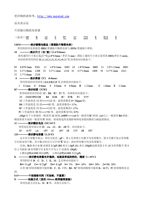
更详细的请参考:品名表示法片状独石陶瓷电容器(品名)GR M 18 8 R7 1C 225 K E15 DGRM————表示镀锡电极品(普通贴片陶瓷电容)常用的村田电容就是GRM普通贴片陶瓷电容与GNM普通贴片排容。
18 ————表示尺寸(长*宽)(1.6*0.8mm)国内通用尺寸表示是(长*宽)1.6*0.8mm(单位为mm).国际上通用尺寸表示是用英0603(单位为inch),村田的常用代码有03,15,18,21,31,32,42,43,55等,具体的对应值如下:03----0.6*0.3mm----0201 15----1.0*0.5mm----0402 18----1.6*0.8mm----0603 21----2.0*1.25mm----0805 31----3.2*1.6mm----1206 32----3.2*1.5mm----1210 42----4.5*2.0mm----1808 43----4.5*3.2mm----1812 55----5.7*5.0mm----22208 ————表示厚度(T)(0.8mm)常用厚度村田代码有5,6,8,9,B,C,E等,具体的对应值如下:5----0.5mm 6----0.6mm 8----0.8mm 9----0.9mm B----1.25mm C----1.6mm E----2.5mmR7 ————表示材质(X7R)常用材质村田代码有5C,R6,R7,F5等,具体的对应值如下:5C----COG/NPO/CH R6----X5R R7----X7R F5-----Y5V5C工作温度是-55度——+125度,温度系数是0+-30ppm/度;R6工作温度是-55度——+85度,温度系数是+-15%;R7工作温度是-55度——+125度,温度系数是+-15%;F5工作温度是-30度——+85度。
温度系数是+22,-82%100pf以下小容值的一般采用5C材质,100PF——1uf的一般采用R7材质,1uf以上一般采用R6材质,精度要求不高的一般采用F5材质。
SMT物料最小包装

1206 SOD-123
30 2980101000476 31 2980101000488 32 2980101000487
GRM1555C1H102JA01D RTT02393JTH RTT02682JTH
0402 0402 0402
33 2980101000293 MPIH252012-1R5M-LF-Z SMD25_20
0402 0402 0402
6 2980101000502 7 2980101000468 8 2980101000343
CL05A475MP5NRNC RTT02102JTH RTT02473JTH
0402 0402 0402
9 2980101000334 GRM155R61A105K 10 3180280200019 ES0603V014CT
10000 10000 10000
功率电感 MPIH252012-1R5M-LF-Z 2.5*2.0*1.2 1.5uH ±20% CH 0402封装贴片电容 4.7pF ±0.5pF 50V MURATA GRM1555C1H4R7CA01D CH 0402封装贴片电阻 100K ±1% RTT02104FTH CH 0402封装贴片电阻 130K ±1% RTT02134FTH CH 0402封装贴片电阻 240R ±1% RTT02241FTH CH 0402封装贴片电阻 30K ±5% RTT02303JTH CH 1206封装贴片电容 22uF ±10% 16V MURATA GRM31CR61C226KE15L CH 0402封装贴片电容 10nF ±10% 50V MURATA GRM155R71H103KA88D CH 0402封装贴片电容 10pF ±5% 50V MURATA GRM1555C1H100JA01D CH 0402封装贴片电容 2.2pF ±0.25pF 50V SAMSUNG CL05C2R2CB5NNNC CH 0402封装贴片电容 2.2uF ±10% 16V MURATA GRM155R61C225KE44D CH 0402封装贴片电容 4.7nF ±10% 50V SAMSUNG CL05B472KB5NNNC CH 0402封装贴片电容 8pF ±5% 50V MURATA GRM1555C1H8R0C CH 0402封装贴片电阻 150K ±1% RTT021503FTH CH 0402封装贴片电阻 2K2 ±5% RTT02222JTH CH 0603封装贴片电容 330nF ±10% 16V MURATA GRM188R71C334KA01D CH AO3401A 贴片MOS管 P SOT-23 CH 功率电感 MPIT4018-2R2M-LF 4.0*4.0*1.8 2.2uH ±20% CH 功率电感 SWPA8040S220MT SMD8*8*4mm 22uH ± 20% CH 集成电路-TJA1042/3/1 SO-8 晶振 AH03270001 32.768KHz SMD3215 贴片电感 JSRF3225-601P 3.2*2.5 600R CH 贴片电解电容 VZH221M1ATR-0806 220uF 10V 0806 ±20% CH 贴片电解电容VZH221M1ETR0810 220uF 25V 0810 ±20% 0805封装贴片电阻 0R ±5% RTT05000JTH 1206封装贴片电阻 10R ±5% RTT06100JTH CH
村田电容大全

村田排容:在一个介质体内由多个电容元件组合而成的独石电容器,特点:小型且大电容量与单个电容元件相比可获得更大的静电电容量,可实现高密度贴装,从而能缩小贴装面积和节约贴装成本
GNM314R71E104MA11D
GNM314R71C104MA01L
GNM2145C1H221KD01D
LLL317R71H473MA01L
LLL215R71A154MA11L
LLL185R71C473MA01L
LLL317R71H223MA01L
LLL315R71E473MA11L
LLL216R71H223MA01L
LLL31MR70J475MA01L
LLL315R71C224MA11L
GJM0336C1E180JB01D
GJM1555C1HR20BB01D
GJM1555C1H9R8WB01D
GJM1555C1H6R1BB01D
GJM1555C1H110GB01D
GJM0335C1ER50BB01D
GJM1555C1H1R6WB01D
GJM1555C1HR80WB01D
MA292R0CAN
MA29100JAN
MA29150JAN
MA297R5CAN
MA29820JAN
MA298R2CAN
MA29270JAN
MA29220JAN
MA291R5CAN
MA291R0CAN
MA29560JAN
MA29102JAN
MA19330JAN
村田低ESR电容器:ESR是Equivalent Series Resistance的缩写,即“等效串联电阻”。理想的电容自身不会有任何能量损失,但实际上,因为制造电容的材料有电阻,电容的绝缘介质有损耗。这个损耗在外部,表现为就像一个电阻跟电容串联在一起,所以就称为“等效串联电阻”。有的电容还会标出ESR值(等效串联电阻),ESR越低,损耗越小,输出电流就越大,电容器的品质越高
Freescale 高功率放大器驱动器或前端放大器 MMG20241H说明书
MMG20241HT1MMG20241HT11Driver or Pre--driver Amplifierfor Doherty Power AmplifiersGaAs Enhancement Mode pHEMTThe MMG20241H is a 1/4W high gain amplifier designed as a driver or pre--driver for Doherty power amplifiers in wireless infrastructure equipment operating in the 450to 3800MHz frequency range.Because of its versatile design,the device may also be used in a variety of general purpose amplifier applications,including frequencies below 450MHz and above 3800MHz.Features ∙P1dB:24dBm @2655MHz ∙Gain:17.8dB @2655MHz∙Designed as a Doherty PA Driver or Pre--driver ∙5V Single Supply,78mA Current ∙SOT--89Package∙50Ohm Operation with Minimal External Matching∙In Tape and Reel.T1Suffix =1,000Units,12mm Tape Width,7--inch Reel.Table 1.Typical Performance (1)CharacteristicSymbol 1915MHz2140MHz 2350MHz2595MHz 2655MHz 3700MHz Unit Small--Signal Gain (S21)G p 2019.51817.517.814.7dB Power Output @1dB Compression P1dB 24.524.523.82423.924.1dBm Third Order Output Intercept Point OIP334.93734.937.53838.1dBm Input Return Loss (S11)IRL –19–24–12–14–14–17dB Output Return Loss (S22)ORL –11–13–18–14–16–15dB Noise FigureNF1.921.92.22.11.9dBTable 2.Maximum RatingsRatingSymbol Value Unit Supply Voltage V DD 6V Supply Current I DD 130mA RF Input PowerP in 23dBm Storage Temperature Range T stg –65to +150︒C Junction TemperatureT J175︒CTable 3.Thermal CharacteristicsCharacteristicSymbol Value (2)Unit Thermal Resistance,Junction to CaseCase Temperature 88︒C,5Vdc,85mA,no RF appliedR θJC57︒C/W1.V DD =5Vdc,T A =25︒C,50ohm system,application circuit tuned for specified frequency.2.Refer to AN1955,Thermal Measurement Methodology of RF Power Amplifiers.Go to /rf.Select Documentation/Application Notes --AN1955.Freescale Semiconductor Technical DataDocument Number:MMG20241HRev.2,9/2014MMG20241HT1SOT--89450–3800MHz,17.8dB @2655MHz24.5dBmDRIVER AMPLIFIER2RF Device DataFreescale Semiconductor,Inc.MMG20241HT1Table 4.Electrical Characteristics (V DD =5Vdc,2140MHz,T A =25︒C,50ohm system,in Freescale Application Circuit)CharacteristicSymbol Min Typ Max Unit Small--Signal Gain (S21)G p 18.419.5—dB Power Output @1dB Compression P1dB —24.5—dBm Third Order Output Intercept Point OIP3—37—dBm Input Return Loss (S11)IRL —–24—dB Output Return Loss (S22)ORL —–13—dB Noise FigureNF —2—dB Supply Current I DD 6478104mA Supply VoltageV DD—5—VTable 5.Functional Pin DescriptionPin NumberPin Function1RF in 2Ground3RF out /DC SupplyTable 6.ESD Protection CharacteristicsTest MethodologyClass Human Body Model (per JESD 22--A114)1A Machine Model (per EIA/JESD 22--A115)A Charge Device Model (per JESD 22--C101)IVTable 7.Moisture Sensitivity LevelTest MethodologyRating Package Peak TemperatureUnit Per JESD22--A113,IPC/JEDEC J--STD--0201260︒CMMG20241HT13RF Device DataFreescale Semiconductor,Inc.50OHM APPLICATION CIRCUIT:2110–2170MHzFigure 2.MMG20241HT1Test Circuit SchematicDDTable 8.MMG20241HT1Test Circuit Component Designations and ValuesPartDescriptionPart NumberManufacturer C1 3.0pF Chip Capacitor GRM1555C1H3R0BB01B Murata C20.4pF Chip Capacitor RVEVK105CH0R4BW--F Taiyo Yuden C30.7pF Chip Capacitor RVEVK105CH0R7BW--F Taiyo Yuden C456pF Chip Capacitor GRM188RC1H560GA01D Murata C50.1μF Chip Capacitor GRM188R71H104KA93D Murata C6 5.6pF Chip Capacitor GRM1555C1H5R6BA01D Murata L130nH Chip Inductor0603CS-30NXJLW Coilcraft PCBIsola IS680-338,0.010",εr =3.38M31382MTL4RF Device Data Freescale Semiconductor,Inc.MMG20241HT150OHM APPLICATION CIRCUIT:2110–2170MHz Figure3.MMG20241HT1Test Circuit Component LayoutPCB actual size:1"⨯1".Table8.MMG20241HT1Test Circuit Component Designations and ValuesPart Description Part Number Manufacturer C1 3.0pF Chip Capacitor GRM1555C1H3R0BB01B MurataC20.4pF Chip Capacitor RVEVK105CH0R4BW--F Taiyo YudenC30.7pF Chip Capacitor RVEVK105CH0R7BW--F Taiyo YudenC456pF Chip Capacitor GRM188RC1H560GA01D MurataC50.1μF Chip Capacitor GRM188R71H104KA93D MurataC6 5.6pF Chip Capacitor GRM1555C1H5R6BA01D MurataL130nH Chip Inductor0603CS-30NXJLW CoilcraftPCB Isola IS680-338,0.010",εr=3.38M31382MTL(Test Circuit Component Designations and Values table repeated for reference.)MMG20241HT15RF Device DataFreescale Semiconductor,Inc.50OHM TYPICAL CHARACTERISTICS:2110–2170MHz32403620002075215022252300383417212000f,FREQUENCY (MHz)Figure 4.Small--Signal Gain (S21)versusFrequency versus Temperature19G p ,S M A L L --S I G N A L G A I N (d B )20182075215022252300--30--5f,FREQUENCY (MHz)Figure 5.Input Return Loss (S11)versusFrequency versus TemperatureI R L ,I N P U T R E T U R N L O S S (d B )--1520002075215022252300--10--20--25--5f,FREQUENCY (MHz)Figure 6.Output Return Loss (S22)versusFrequency versus TemperatureO R L ,O U T P U T R E T U R N L O S S (d B )--1520002075215022252300--10--2022262423f,FREQUENCY (MHz)Figure 7.P1dB versus Frequency versusTemperatureP 1d B ,1d B C O M P R E S S I O N P O I N T (d B m )2520002075215022252300f,FREQUENCY (MHz)Figure 8.Third Order Output Intercept Point versus Frequency versus Temperature O I P 3,T H I R D O R D E R O U T P U T I N T E R C E P T P O I N T (d B m )13f,FREQUENCY (MHz)Figure 9.Noise Figure versus Frequencyversus Temperature21.5N F ,N O I S E F I G U R E (d B )2.520002075215022252300--256RF Device Data Freescale Semiconductor,Inc.MMG20241HT150OHM TYPICAL CHARACTERISTICS:2110–2170MHz --55--159P out,OUTPUT POWER(dBm)Figure10.Single--Carrier W--CDMA Adjacent Channel Power Ratio versus Output Power versus Temperature --25--35--4524211512ACPR,ADJACENTCHANNELPOWERRATIO(dBc)18MMG20241HT17RF Device DataFreescale Semiconductor,Inc.50OHM APPLICATION CIRCUIT:2620–2690MHzFigure 11.MMG20241HT1Test Circuit SchematicDDTable 9.MMG20241HT1Test Circuit Component Designations and ValuesPartDescriptionPart NumberManufacturer C1 1.5pF Chip Capacitor GRM1555C1H1R5BA01D Murata C21pF Chip Capacitor GRM1555C1H1R0BA01D Murata C356pF Chip Capacitor GRM188RC1H560GA01D Murata C40.1μF Chip Capacitor GRM188R71H104KA93D Murata L11nH Chip Inductor 0402CS-1N0XJLW Coilcraft L28.2nH Chip Inductor0603CS-8N2XJL Coilcraft PCBIsola IS680-338,0.010",εr =3.38M31382MTL8RF Device Data Freescale Semiconductor,Inc.MMG20241HT150OHM APPLICATION CIRCUIT:2620–2690MHz Figure12.MMG20241HT1Test Circuit Component LayoutPCB actual size:1"⨯1".Table9.MMG20241HT1Test Circuit Component Designations and ValuesPart Description Part Number Manufacturer C1 1.5pF Chip Capacitor GRM1555C1H1R5BA01D MurataC21pF Chip Capacitor GRM1555C1H1R0BA01D MurataC356pF Chip Capacitor GRM188RC1H560GA01D MurataC40.1μF Chip Capacitor GRM188R71H104KA93D MurataL11nH Chip Inductor0402CS-1N0XJLW CoilcraftL28.2nH Chip Inductor0603CS-8N2XJL CoilcraftPCB Isola IS680-338,0.010",εr=3.38M31382MTL(Test Circuit Component Designations and Values table repeated for reference.)MMG20241HT19RF Device DataFreescale Semiconductor,Inc.50OHM TYPICAL CHARACTERISTICS:2620–2690MHz36403825002575265027252800393715192500f,FREQUENCY (MHz)Figure 13.Small--Signal Gain (S21)versus Frequency17G p ,S M A L L --S I G N A L G A I N (d B )18162575265027252800--4f,FREQUENCY (MHz)Figure 14.Input Return Loss (S11)versusFrequencyI R L ,I N P U T R E T U R N L O S S (d B )--1225002575265027252800--8--16--28--4f,FREQUENCY (MHz)Figure 15.Output Return Loss (S22)versusFrequencyO R L ,O U T P U T R E T U R N L O S S (d B )--1225002575265027252800--8--1623252423.5f,FREQUENCY (MHz)Figure 16.P1dB versus FrequencyP 1d B ,1d B C O M P R E S S I O N P O I N T (d B m )24.525002575265027252800f,FREQUENCY (MHz)Figure 17.Third Order Output InterceptPoint versus FrequencyO I P 3,T H I R D O R D E R O U T P U T I N T E R C E P T P O I N T (d B m )1.63.2f,FREQUENCY (MHz)Figure 18.Noise Figure versus Frequency2.42N F ,N O I S E F I G U R E (d B )2.825002575265027252800--20--20--2450OHM APPLICATION CIRCUIT:1805–2025MHzFigure 19.MMG20241HT1Test Circuit SchematicDDTable10.MMG20241HT1Test Circuit Component Designations and ValuesPartDescriptionPart NumberManufacturer C1 3.6pF Chip Capacitor GRM1555C1H3R6BB01B Murata C20.4pF Chip Capacitor RVEVK105CH0R4BW Taiyo Yuden C30.6pF Chip Capacitor RVEVK105CH0R6BW Taiyo Yuden C456pF Chip Capacitor GRM188RC1H560GA01D Murata C50.1μF Chip Capacitor GRM188R71H104KA93D Murata C610pF Chip Capacitor GRM1555C1H100JA01D Murata L133nH Chip Inductor0603CS--33NXJLW Coilcraft PCBIsola IS680-338,0.010",εr =3.38M31382MTL50OHM APPLICATION CIRCUIT:1805–2025MHzFigure 20.MMG20241HT1Test Circuit Component LayoutPCB actual size:1"⨯1".Table 10.MMG20241HT1Test Circuit Component Designations and ValuesPartDescriptionPart NumberManufacturer C1 3.6pF Chip Capacitor GRM1555C1H3R6BB01B Murata C20.4pF Chip Capacitor RVEVK105CH0R4BW Taiyo Yuden C30.6pF Chip Capacitor RVEVK105CH0R6BW Taiyo Yuden C456pF Chip Capacitor GRM188RC1H560GA01D Murata C50.1μF Chip Capacitor GRM188R71H104KA93D Murata C610pF Chip Capacitor GRM1555C1H100JA01D Murata L133nH Chip Inductor0603CS--33NXJLW Coilcraft PCBIsola IS680-338,0.010",εr =3.38M31382MTL(Test Circuit Component Designations and Values table repeated for reference.)50OHM TYPICAL CHARACTERISTICS:1805–2025MHz17211700f,FREQUENCY (MHz)Figure 21.Small--Signal Gain (S21)versus Frequency19G p ,S M A L L --S I G N A L G A I N (d B )20181800190020002100--5f,FREQUENCY (MHz)Figure 22.Input Return Loss (S11)versusFrequencyI R L ,I N P U T R E T U R N L O S S (d B )--1517001800190020002100--10--20--25--12--8f,FREQUENCY (MHz)Figure 23.Output Return Loss (S22)versusFrequencyO R L ,O U T P U T R E T U R N L O S S (d B)--1017001800190020002100--9--1122262423f,FREQUENCY (MHz)Figure 24.P1dB versus FrequencyP 1d B ,1d B C O M P R E S S I O N P O I N T(d B m )2517001800190020002100303834170018001900200021003632f,FREQUENCY (MHz)Figure 25.Third Order Output InterceptPoint versus FrequencyO I P 3,T H I R D O R D E R O U T P U T I N T E R C E P T P O I N T (d B m )1.22.8f,FREQUENCY (MHz)Figure 26.Noise Figure versus Frequency21.6N F ,N O I S E F I G UR E (d B )2.41700180019002000210050OHM APPLICATION CIRCUIT:2300–2400MHzFigure 27.MMG20241HT1Test Circuit SchematicRF INPUTDDTable 11.MMG20241HT1Test Circuit Component Designations and ValuesPartDescriptionPart NumberManufacturer C12pF Chip Capacitor GRM1555C1H2R0BA01D Murata C2 1.3pF Chip Capacitor GRM1555C1H1R3BA01D Murata C356pF Chip Capacitor GRM188RC1H560GA01D Murata C40.1μF Chip Capacitor GRM188R71H104KA93D Murata L11nH Chip Inductor 0402CS--1N0XJLW Coilcraft L28.2nH Chip Inductor0603CS--8N2XJL Coilcraft PCBIsola IS680-338,0.010",εr =3.38M31382MTL50OHM APPLICATION CIRCUIT:2300–2400MHzFigure 28.MMG20241HT1Test Circuit Component LayoutPCB actual size:1"⨯1".Table 11.MMG20241HT1Test Circuit Component Designations and ValuesPartDescriptionPart NumberManufacturer C12pF Chip Capacitor GRM1555C1H2R0BA01D Murata C2 1.3pF Chip Capacitor GRM1555C1H1R3BA01D Murata C356pF Chip Capacitor GRM188RC1H560GA01D Murata C40.1μF Chip Capacitor GRM188R71H104KA93D Murata L11nH Chip Inductor 0402CS--1N0XJLW Coilcraft L28.2nH Chip Inductor0603CS--8N2XJL Coilcraft PCBIsola IS680-338,0.010",εr =3.38M31382MTL(Test Circuit Component Designations and Values table repeated for reference.)50OHM TYPICAL CHARACTERISTICS:2300–2400MHzO R L ,O U T P U T R E T U R N L O S S (d B )15192200f,FREQUENCY (MHz)Figure 29.Small--Signal Gain (S21)versus Frequency17G p ,S M A L L --S I G N A L G A I N (d B )18162275235024252500--4f,FREQUENCY (MHz)Figure 30.Input Return Loss (S11)versusFrequencyI R L ,I N P U T R E T U R N L O S S (d B )--1222002275235024252500--8--16--20--45--5f,FREQUENCY (MHz)Figure 31.Output Return Loss (S22)versusFrequency--2522002275235024252500--15--3521252322f,FREQUENCY (MHz)Figure 32.P1dB versus FrequencyP 1d B ,1d B C O M PR E S S I O N P O I N T (d B m )2422002275235024252500303834220022752350242525003632f,FREQUENCY (MHz)Figure 33.Third Order Output InterceptPoint versus FrequencyO I P 3,T H I R D O R D E R O U T P U T I N T E R C E P T P O I N T (dBm )1.22.8f,FREQUENCY (MHz)Figure 34.Noise Figure versus Frequency21.6N F ,N O I S E F I G U R E (d B )2.42200227523502425250050OHM APPLICATION CIRCUIT:2570–2620MHzFigure 35.MMG20241HT1Test Circuit SchematicDDTable 12.MMG20241HT1Test Circuit Component Designations and ValuesPartDescriptionPart NumberManufacturer C1 1.5pF Chip Capacitor GRM1555C1H1R5BA01D Murata C22pF Chip Capacitor GRM1555C1H2R0BA01D Murata C356pF Chip Capacitor GRM188RC1H560GA01D Murata C40.1μF Chip Capacitor GRM188R71H104KA93D Murata L11nH Chip Inductor 0402CS--1N0XJLW Coilcraft L28.2nH Chip Inductor0603CS--8N2XJL Coilcraft PCBIsola IS680-338,0.010",εr =3.38M31382MTL50OHM APPLICATION CIRCUIT:2570–2620MHzPCB actual size:1"⨯1".Figure36.MMG20241HT1Test Circuit Component LayoutTable12.MMG20241HT1Test Circuit Component Designations and ValuesPart Description Part Number Manufacturer C1 1.5pF Chip Capacitor GRM1555C1H1R5BA01D MurataC22pF Chip Capacitor GRM1555C1H2R0BA01D MurataC356pF Chip Capacitor GRM188RC1H560GA01D MurataC40.1μF Chip Capacitor GRM188R71H104KA93D MurataL11nH Chip Inductor0402CS--1N0XJLW CoilcraftL28.2nH Chip Inductor0603CS--8N2XJL CoilcraftPCB Isola IS680-338,0.010",εr=3.38M31382MTL(Test Circuit Component Designations and Values table repeated for reference.)50OHM TYPICAL CHARACTERISTICS:2570–2620MHzO R L ,O U T P U T R E T U R N L O S S (d B )15192450f,FREQUENCY (MHz)Figure 37.Small--Signal Gain (S21)versus Frequency17G p ,S M A L L --S I G N A L G A I N (d B )18162525260026752750f,FREQUENCY (MHz)Figure 38.Input Return Loss (S11)versusFrequencyI R L ,I N P U T R E T U R N L O S S (d B )--1624502525260026752750--8--24--32--25--5f,FREQUENCY (MHz)Figure 39.Output Return Loss (S22)versusFrequency--1524502525260026752750--10--2021252322f,FREQUENCY (MHz)Figure 40.P1dB versus FrequencyP 1d B ,1d B C O M P R E S S I O N P O I NT (d B m )2424502525260026752750324036245025252600267527503834f,FREQUENCY (MHz)Figure 41.Third Order Output InterceptPoint versus FrequencyO I P 3,T H I R D O R D E R O U T P U T I N T E R C E P T P O I N T (dBm )1.22.8f,FREQUENCY (MHz)Figure 42.Noise Figure versus Frequency21.6N F ,N O I S E F I G U R E (d B )2.42450252526002675275050OHM APPLICATION CIRCUIT:3600–3800MHzFigure 43.MMG20241HT1Test Circuit SchematicDDTable13.MMG20241HT1Test Circuit Component Designations and ValuesPartDescriptionPart NumberManufacturer C10.6pF Chip Capacitor RVEVK105CH0R6BW--F Taiyo Yuden C21pF Chip Capacitor GJM1555C1H1R0CB01D Murata C30.01μF Chip Capacitor GRM155R71E103KA01D Murata C456pF Chip Capacitor GRM188RC1H560GA01D Murata C50.1μF Chip Capacitor GRM188R71H104KA93D Murata L11nH Chip Inductor 0402CS-1N0XJLW Coilcraft L2 2.7nH Chip Inductor LQG15HS2N7S02Murata L382nH Chip Inductor0603CS-82NX_LW Coilcraft PCBIsola IS680-338,0.010",εr =3.38M31382MTL20RF Device Data Freescale Semiconductor,Inc.MMG20241HT150OHM APPLICATION CIRCUIT:3600–3800MHz Figure44.MMG20241HT1Test Circuit Component LayoutPCB actual size:1"⨯1".Note:Components L2and C3are connected together in series.Table13.MMG20241HT1Test Circuit Component Designations and ValuesPart Description Part Number Manufacturer C10.6pF Chip Capacitor RVEVK105CH0R6BW--F Taiyo YudenC21pF Chip Capacitor GJM1555C1H1R0CB01D MurataC30.01μF Chip Capacitor GRM155R71E103KA01D MurataC456pF Chip Capacitor GRM188RC1H560GA01D MurataC50.1μF Chip Capacitor GRM188R71H104KA93D MurataL11nH Chip Inductor0402CS-1N0XJLW CoilcraftL2 2.7nH Chip Inductor LQG15HS2N7S02MurataL382nH Chip Inductor0603CS-82NX_LW CoilcraftPCB Isola IS680-338,0.010",εr=3.38M31382MTL(Test Circuit Component Designations and Values table repeated for reference.)MMG20241HT121RF Device DataFreescale Semiconductor,Inc.50OHM TYPICAL CHARACTERISTICS:3600–3800MHz3500360037003800390035003600370038003900350036003700380039003500360037003800390035003600370038003900364038393711153500f,FREQUENCY (MHz)Figure 45.Small--Signal Gain (S21)versus Frequency13G p ,S M A L L --S I G N A L G A I N (d B )14123600370038003900--4f,FREQUENCY (MHz)Figure 46.Input Return Loss (S11)versusFrequencyI R L ,I N P U T R E T U R N L O S S (d B )--12--8--16--24--8f,FREQUENCY (MHz)Figure 47.Output Return Loss (S22)versusFrequencyO R L ,O U T P U T R E T U R N L O S S (d B )--16--12--2023252423.5f,FREQUENCY (MHz)Figure 48.P1dB versus FrequencyP 1d B ,1d B C O M P R E S S I O N P O I N T (d B m )24.5f,FREQUENCY (MHz)Figure 49.Third Order Output InterceptPoint versus FrequencyO I P 3,T H I R D O R D E R O U T P U T I N T E R C E P T P O I N T (d B m )1.53.1f,FREQUENCY (MHz)Figure 50.Noise Figure versus Frequency2.31.9N F ,N O I S E F I G U R E (d B )2.7--2022RF Device Data Freescale Semiconductor,Inc.MMG20241HT1Figure51.PCB Pad Layout for SOT--89AM20241AWLYWZ Figure52.Product MarkingMMG20241HT123RF Device DataFreescale Semiconductor,Inc.PACKAGEDIMENSIONS24RF Device Data Freescale Semiconductor,Inc.MMG20241HT1MMG20241HT125 RF Device DataFreescale Semiconductor,Inc.26RF Device DataFreescale Semiconductor,Inc.MMG20241HT1PRODUCT DOCUMENTATION,SOFTWARE AND TOOLSRefer to the following resources to aid your design process.Application Notes∙AN1955:Thermal Measurement Methodology of RF Power Amplifiers Software ∙.s2p FileDevelopment Tools ∙Printed Circuit BoardsFor Software and Tools,do a Part Number search at ,and select the “Part Number”link.Go to Software &Tools on the part’s Product Summary page to download the respective tool.FAILURE ANALYSISAt this time,because of the physical characteristics of the part,failure analysis is limited to electrical signature analysis.In cases where Freescale is contractually obligated to perform failure analysis (FA)services,full FA may be performed by third party vendors with moderate success.For updates contact your local Freescale Sales Office.REVISION HISTORYThe following table summarizes revisions to this document.RevisionDate Description0Apr.2014∙Initial Release of Data Sheet1July 2014∙Table 2,Maximum Ratings:updated Junction Temperature from 150︒C to 175︒C to reflect recent test results of the device,p.1∙Fig.2,Test Circuit Schematic for 2110--2170MHz:changed pin 4to pin 2to reflect correct pin numbers,p.3∙Added application circuit for 1805–2025MHz as follows:schematic,component designations and values,component layout,and typical characteristic performance graphs,pp.10–12∙Added application circuit for 2300–2400MHz as follows:schematic,component designations and values,component layout,and typical characteristic performance graphs,pp.13–15∙Added application circuit for 2570–2620MHz as follows:schematic,component designations and values,component layout,and typical characteristic performance graphs,pp.16–182Sept.2014∙Typical Performance table:added 3700MHz performance values,p.1∙Added application circuit for 3600–3800MHz as follows:schematic,component designations and values,component layout,and typical characteristic performance graphs,pp.19–21MMG20241HT127Information in this document is provided solely to enable system and softwareimplementers to use Freescale products.There are no express or implied copyright licenses granted hereunder to design or fabricate any integrated circuits based on the information in this document.Freescale reserves the right to make changes without further notice to any products herein.Freescale makes no warranty,representation,or guarantee regarding the suitability of its products for any particular purpose,nor does Freescale assume any liability arising out of the application or use of any product or circuit,and specifically disclaims any and all liability,including without limitation consequential or incidental damages.“Typical”parameters that may be provided in Freescale data sheets and/or specifications can and do vary in different applications,and actual performance may vary over time.All operating parameters,including “typicals,”must be validated for each customer application by customer’s technical experts.Freescale does not convey any license under its patent rights nor the rights of others.Freescale sells products pursuant to standard terms and conditions of sale,which can be found at the following address:/SalesTermsandConditions.Freescale and the Freescale logo are trademarks of Freescale Semiconductor,Inc.,Reg.U.S.Pat.&Tm.Off.All other product or service names are the property of their respective owners.E 2014Freescale Semiconductor,Inc.How to Reach Us:Home Page: Web Support:/supportMMG20241HT1。
GRM1555C1H102JA01D 中文资料 最新

注意
1. 本目录是从株式会社村田制作所网站中下载的。
规格若有变更,或若其中产品停产,请在订购时确认,恕不另行通知。
外观&形状
参考信息
在1 / 4页
注意
1. 本目录是从株式会社村田制作所网站中下载的。
规格若有变更,或若其中产品停产,请在订购时确认,恕不另行通知。
规格
在2 / 4页
注意
1. 本目录是从株式会社村田制作所网站中下载的。
规格若有变更,或若其中产品停产,请在订购时确认,恕不另行通知。
特性数据
同特性的产品可能用不同的型号表示。
在3 / 4页
注意
1. 本目录是从株式会社村田制作所网站中下载的。
规格若有变更,或若其中产品停产,请在订购时确认,恕不另行通知。
在4 / 4页。
EXCEL比较工具试用版
MAIN MAIN MAIN MAIN MAIN MAIN MAIN MAIN MAIN MAIN MAIN MAIN MAIN MAIN MAIN MAIN MAIN
MAIN MAIN MAIN MAIN MAIN MAIN MAIN MAIN MAIN MAIN MAIN MAIN MAIN MAIN MAIN MAIN MAIN MAIN MAIN
MAIN
MAIN
SUB SUB
MAIN
SUB
SUB MAIN SUB SUB
MAIN SUB
SUB MAIN
SUB SUB MAIN
SUB
SUB
MAIN SUB MAIN MAIN SUB SUB SUB SUB MAIN MAIN MAIN MAIN SUB MAIN SUB SUB MAIN MAIN MAIN
MAIN SUB MAIN MAIN SUB MAIN
MAIN
WRN:替代料和主料位号不一致,可能是配置表省略替代物料处理WRN:替代料和主料位号不一致,可能是配置表省略替代物料处理
WRN:替代料和主料位号不一致,可能是配置表省略替代物料处理WRN:替代料和主料位号不一致,可能是配置表省略替代物料处理
WRN:替代料和主料位号不一致,可能是配置表省略替代物料处理。
GRM1555C1H331JA01J;中文规格书,Datasheet资料

/
/
分销商库存信息:
MURATA GRM1555C1H331JA01J
180mm Paper Tape
J
330mm Paper Tape
Hale Waihona Puke CBulk Case
B
Bulk(Bag)
Minimum Quantity 10000 50000 50000 1000
I Specifications
Please refer to 'GRM Series Specification and Test Methods (1)' PDF file.
melting point is used. Please confirm the solderability of Tin plating termination chip before use. o Use of Sn-Zn based solder will deteriorate reliability of MLCC. Please check with our sales represetatives for the use of Sn-Zn based solder in advance.
• The RoHS compliance means that we judge from EU Directive 2002/95/EC the products do not contain lead, cadmium, mercury, hexavalent chromium, PBB and PBDE, except exemptions stated in EU Directive 2002/95/EC annex and impurities existing in natural world.
GRM1555C1H100JA01D中文资料
物料编号:GRM1555C1H100JA01D的详细参数_易容网
MLCC即是多层陶瓷电容片式,是电子信息产品不可或缺的基本组件之一。
我国MLCC的生产起步在80年代初,行业早期主要是在外资企业的带动下发展起来的,近年来国内企业在技术上实现突破,行业国产化成效显著,并推动了MLCC产量迅速增长。
目前,MLCC的应用领域已从手机、电脑、电视机等消费电子领域,逐步拓展到新能源发电、新能源汽车、节能灯具、轨道交通、直流输变电、三网融合、高清电视、机顶盒、手机电视等多个行业。
对于这个悄悄活跃在人们生活中的元件你又知道多少呢.
本次易容网为大家推荐比较常用的MLCC村田 | Murata品牌的料号GRM1555C1H100JA01D的相关参数
易容网是深圳市易容信息技术有限公司独自研发的全球最大的MLCC搜索采购服务网站,2014年创立于深圳市南山区,全国首家电子元器件行业电容元件的搜索引擎及o2o商务服务平台。
易容网()现已建成全球最大的MLCC电容搜索引擎数据库,包含全球25家电容生产厂商超过28万组MLCC产品数据,用户可根据行业应用、物料编号、规格参数等信息快速的找到所有相关的MLCC电容数据。
易容网在搜索服务的前提下还提供村田、TDK、国巨、太阳诱电、风华高科等常见品牌产品的o2o商务服务,让企业客户实现询价、报价、在线订单、出库、实时物流、签收、账期服务等在线一站式商务服务体验。
- 1、下载文档前请自行甄别文档内容的完整性,平台不提供额外的编辑、内容补充、找答案等附加服务。
- 2、"仅部分预览"的文档,不可在线预览部分如存在完整性等问题,可反馈申请退款(可完整预览的文档不适用该条件!)。
- 3、如文档侵犯您的权益,请联系客服反馈,我们会尽快为您处理(人工客服工作时间:9:00-18:30)。
物料编号:GRM1555C1H471JA01D详细参数_易容网
MLCC即是多层陶瓷电容片式,是电子信息产品不可或缺的基本组件之一。
我国MLCC的生产起步在80年代初,行业早期主要是在外资企业的带动下发展起来的,近年来国内企业在技术上实现突破,行业国产化成效显著,并推动了MLCC产量迅速增长。
目前,MLCC的应用领域已从手机、电脑、电视机等消费电子领域,逐步拓展到新能源发电、新能源汽车、节能灯具、轨道交通、直流输变电、三网融合、高清电视、机顶盒、手机电视等多个行业。
对于这个悄悄活跃在人们生活中的元件你又知道多少呢.
本次易容网为大家推荐比较常用的MLCC村田 | Murata品牌的料号GRM1555C1H471JA01D的相关参数
易容网是深圳市易容信息技术有限公司独自研发的全球最大的MLCC搜索采购服务网站,2014年创立于深圳市南山区,全国首家电子元器件行业电容元件的搜索引擎及o2o商务服务平台。
易容网()现已建成全球最大的MLCC电容搜索引擎数据库,包含全球25家电容生产厂商超过28万组MLCC产品数据,用户可根据行业应用、物料编号、规格参数等信息快速的找到所有相关的MLCC电容数据。
易容网在搜索服务的前提下还提供村田、TDK、国巨、太阳诱电、风华高科等常见品牌产品的o2o商务服务,让企业客户实现询价、报价、在线订单、出库、实时物流、签收、账期服务等在线一站式商务服务体验。
