P8SG-247R2E中文资料
天诚通信-铜产品
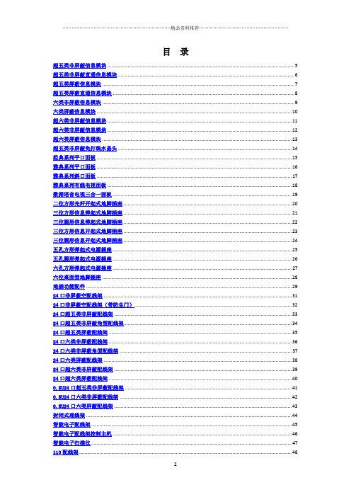
目录超五类非屏蔽信息模块 (5)超五类非屏蔽直通信息模块 (6)超五类屏蔽信息模块 (7)超五类屏蔽直通信息模块 (8)六类非屏蔽信息模块 (9)六类屏蔽信息模块 (10)超六类非屏蔽信息模块 (11)超六类非屏蔽信息模块 (12)超六类屏蔽信息模块 (13)超五类非屏蔽免打线水晶头 (14)经典系列平口面板 (15)雅典系列平口面板 (16)雅典系列斜口面板 (17)雅典系列有线电视面板 (18)数据语音电视三合一面板 (19)二位方形光纤开起式地脚插座 (20)三位方形信息弹起式地脚插座 (21)三位圆形信息弹起式地脚插座 (22)三位方形信息开起式地脚插座 (23)三位圆形信息开起式地脚插座 (24)五孔方形弹起式电源插座 (25)五孔圆形弹起式电源插座 (26)六孔方形弹起式电源插座 (27)六位桌面型地脚插座 (28)地插功能配件 (29)24口非屏蔽空配线架 (31)24口非屏蔽空配线架(带防尘门) (32)24口超五类非屏蔽配线架 (33)24口超五类非屏蔽角型配线架 (34)24口超五类屏蔽配线架 (35)24口六类非屏蔽配线架 (36)24口六类非屏蔽角型配线架 (37)24口六类屏蔽配线架 (38)24口超六类非屏蔽配线架 (39)24口超六类屏蔽配线架 (40)0.5U24口超五类非屏蔽配线架 (41)0.5U24口六类非屏蔽配线架 (42)0.5U24口六类屏蔽配线架 (43)封闭式理线架 (44)智能电子配线架 (45)智能电子配线架控制主机 (46)智能电子扫描仪 (47)110理线架 (49)110连接块 (50)110跳线 (51)110转RJ45跳线 (52)超五类非屏蔽跳线 (53)超五类屏蔽跳线 (54)六类非屏蔽跳线 (55)六类屏蔽跳线 (56)超六类非屏蔽跳线 (57)超六类屏蔽跳线 (58)超五类屏蔽防水跳线 (59)六类屏蔽防水跳线 (60)五类1对非屏蔽线缆 (61)五类2对非屏蔽线缆 (62)五类4对非屏蔽线缆 (63)超五类4对非屏蔽线缆 (64)超五类4对屏蔽线缆 (65)超五类4对双屏蔽线缆 (66)六类4对非屏蔽线缆 (67)六类4对屏蔽线缆 (68)六类4对双屏蔽线缆 (69)六类4对对对屏蔽线缆 (70)超六类4对非屏蔽线缆 (71)超六类4对屏蔽线缆 (72)超六类4对双屏蔽线缆 (73)超六类4对对对屏蔽线缆 (74)七类4对屏蔽线缆 (75)五类4对非屏蔽室外线缆 (76)五类4对屏蔽室外线缆 (77)超五类4对屏蔽室外线缆 (78)超五类4对屏蔽室外线缆 (79)六类4对非屏蔽室外线缆 (80)六类4对屏蔽线缆 (81)五类4对双护套非屏蔽线缆 (82)超五类4对双护套非屏蔽线缆 (83)超五类4对双护套屏蔽线缆 (84)3类非屏蔽室内线缆(50对) (85)5类非屏蔽室内线缆(25对) (86)3类屏蔽室内线缆(50对) (87)5类屏蔽室内线缆(25对) (88)3类非屏蔽室外线缆(50对) (89)5类非屏蔽室外线缆(25对) (90)3类屏蔽室外线缆(50对) (91)5类屏蔽室外线缆(50对) (92)市话充油通信电缆(50对) (94)市话重铠通信电缆(50对) (95)超五类非屏蔽信息模块产品说明:应用范围:1000 BASE-TX千兆以太网;100 BASE-TX快速以太网;10 BASE-T以太网;语音,视频及其它应用网络工作区域内语音、数据信息的连接。
国威电话交换机说明书
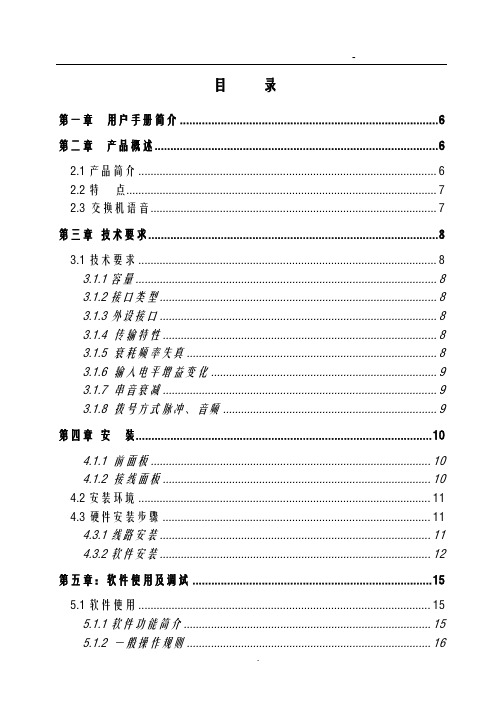
目录第一章用户手册简介 (6)第二章产品概述 (6)2.1产品简介 (6)2.2特点 (7)2.3交换机语音 (7)第三章技术要求 (8)3.1技术要求 (8)3.1.1容量 (8)3.1.2接口类型 (8)3.1.3外设接口 (8)3.1.4 传输特性 (8)3.1.5 衰耗频率失真 (8)3.1.6 输入电平增益变化 (9)3.1.7 串音衰减 (9)3.1.8 拨号方式脉冲、音频 (9)第四章安装 (10)4.1.1 前面板 (10)4.1.2 接线面板 (10)4.2安装环境 (11)4.3硬件安装步骤 (11)4.3.1线路安装 (11)4.3.2软件安装 (12)第五章:软件使用及调试 (15)5.1软件使用 (15)5.1.1软件功能简介 (15)5.1.2 一般操作规则 (16)5.1.4权限管理 (17)5.1.5话务监控 (19)5.1.6押金管理 (19)5.1.7参数设置 (20)5.1.8费率管理 (24)5.1.9话单处理 (27)5.2.0系统 (27)第六章系统编程 (28)6.1系统编程 (28)6.1.1系统功能锁 (28)6.1.2系统初始化(系统清除) (29)6.1.3设置(修改)系统日期 (29)6.1.4分机号长设置 (29)6.1.5中继计费方式设置 (30)6.1.6入中继类型设置 (30)6.1.7中继发码方式设置 (30)6.1.8中继出局方式设置 (30)6.1.9中继出局号设置 (30)6.2.0 批处理代码 (31)6.2.1分机等级设置 (31)6.2.2分机弹性编码 (32)6.2.3话务机设置(修改) (32)6.2.4清除分机密码 (33)6.2.5 系统计费方式 (33)6.2.6 市话计费开关 (33)6.2.7 市话费率设置 (34)6.2.8市话计费延时时间设置 (34)6.2.9 市话、手机手续费和附加费设置 (34)6.3.0特服号码费率设置 (34)6.3.2 本地网(特服号)手续费及附加费设置 (35)6.3.3 国内长途费率设置 (35)6.3.4国内长途手续费和附加费设置 (35)6.3.5国际费率设置 (35)6.3.6预付款超额实时开关 (35)6.3.7国际长途手续费和附加费设置 (35)6.3.8 长途手机费率设置 (36)6.3.9 清除某分机累计话费 (36)6.4.0设置交换机门数 (36)6.4.1 设置分机闹钟服务 (36)6.4.2系统自检 (36)6.4.3 半价折率百分比设置 (36)6.4.4特殊长途手机费率设置 (37)6.4.5 分机特服权设置 (37)6.4.6 分机本地网(郊县)电话权设置 (37)6.4.7内部分机呼叫权设置 (38)6.4.8分机允许中继呼入权设置 (38)6.4.9中继开关设置 (39)6.5.0 中继呼入直拨出错处理设置 (39)6.5.1中继分组设置 (40)6.5.2分机分组中继权设置 (40)6.5.3代理总机设置 (40)6.5.4日/夜自动切换模式及等级 (40)6.5.5引导语音录制 (41)6.5.6手机费率设置 (41)6.5.7手机延时时间设置 (42)6.5.8 分机预付款设置 (42)6.5.9半价时段设置 (42)6.6.0 优惠时段设置 (43)6.6.1 特定优惠率百分比设置 (43)6.6.3分机来电显示 (43)6.6.4中继来电显示设置 (43)6.6.5设置分机呼出时限 (44)6.6.6 附加费类型 (44)6.6.7 设置账号密码及漫游操作 (44)6.6.8账号服务权限 (45)6.6.9 账号预付款 (45)6.7.0 设置账号数量 (45)6.7.1功能首位号设置 (45)6.7.2外线呼入音乐开关 (45)6.7.3 外线连选设置 (46)6.7.4农话权独立设置 (46)6.7.5市话密码限制设置 (46)6.7.6振铃二次来电显示设置 (46)6.7.7 IP字头设置 (46)6.7.8拨总机缩位 (46)6.7.9话务机循环接听 (47)6.8.0外线呼入缩位拨号功能 (47)6.8.1引导语音时长设置 (47)6.8.2内线分组设置 (47)第七章分机操作功能 (47)7.1.1呼叫内部分机 (47)7.1.2呼叫总机 (47)7.1.3呼叫外线 (48)7.1.4指定外线 (48)7.1.5来电转接 (48)7.1.6离位转移 (48)7.1.7免打扰 (48)7.1.8呼叫保护 (49)7.1.9三方通话(电话会议) (49)7.2.0代接来话 (49)7.2.1遇忙转移 (49)7.2.2遇忙回叫 (49)7.2.3密码设置 (49)7.2.4分机功能清除 (50)7.2.5分机查询外线被某分机占用 (50)7.2.6内线热线服务 (50)7.2.7外线热线服务 (50)7.2.8取消内、外线热线服务功能 (50)7.2.9中继呼入 (51)7.3.0外线转外线 (51)7.3.1外线呼叫等待功能 (51)7.3.2强插服务 (52)7.3.3总机代拨功能 (52)7.3.4分机留言功能 (52)7.3.5分机广播功能 (52)7.3.6指定代理总机 (53)7.3.7清除分机密码 (53)7.3.8自报语音服务 (53)7.3.9常见故障排除 (53)RJ45接头接线线序 (55)9A结构图 (57)第八章系统指令表 (59)第一章用户手册简介感谢您购买国威时代ws848系列商务电话交换机!本交换机是专为满足小型企业办公通信需要而设计的。
CG2145MS,CG2800MS,CG75MS,CG75LTR,CG2800LTR,CG2600LTR,CG2470L,CG75L, 规格书,Datasheet 资料

CG/CG2 Series
CG/CG2 Series
Description
Littelfuse highly reliable CG/CG2 Series GDTs provide a high degree of surge protection in a small size ideal for board level circuit protection. GDTs function as switches which dissipate a minimum amount of energy and therefore handle currents that far surpass other types of transient voltage protection. Their gas-filled, rugged ceramic metal construction make them well suited to adverse environments. The CG/CG2 series comes in a variety of forms including surface mount, core, straight and shaped leads, to serve a variety of mounting methods.
AGENCY FILE NUMBER
Agency Approvals
AGENCY
& &
2 Electrode GDT Graphical Symbol
The CG Series (75-110V) is ideal for protection of test and communication equipment and other devices in which low voltage limits and extremely low arc voltages are required. The CG2 Series (145V-1000V) is ideal for protecting equipment where higher voltage limits and holdover voltages are necessary.
Cisco SGE2000P 24-Port Gigabit Switch PoE 产品概述说明书

Data Sheet Cisco SGE2000P 24-Port Gigabit Switch: PoECisco Small Business Managed SwitchesHigh-Performance, Secure Switching with PoE for Small BusinessesHighlights●24 high-speed ports optimized for the network core or to support bandwidth-intensive applications●Resilient Clustering provides the ability to add more switches as needed and to manage the stack as a singleswitch, to support growing businesses●Power over Ethernet easily and cost-effectively powers wireless access points, video cameras, and othernetwork-connected endpoints●Strong security protects network traffic to keep unauthorized users off the network●Intelligent QoS helps ensure a consistent network experience and supports networked applications includingvoice, video, and data storage●Limited lifetime warrantyFigure 1. Cisco SGE2000P 24-Port Gigabit Switch: PoEProduct OverviewThe Cisco® SGE2000P 24-Port Gigabit Switch (Figure 1) helps maximize system availability, with fully redundant stacking and dual images for resilient firmware upgrades. The switch helps secure the network through IEEE 802.1Q VLANs, IEEE 802.1X port authentication, access control lists (ACL), denial-of-service (DoS) prevention, and MAC-based filtering. The enhanced quality of service (QoS) and traffic-management features help ensure clear and reliable IP voice and video communications.For wireless or voice over IP (VoIP) deployments, the Cisco SGE2000P supports the IEEE802.3af standard for Power over Ethernet (PoE). Automatic load sensing in the power control circuitry automatically detects PoE on the end device before providing power. For safety, each port has independent overload and short-circuit protection, along with LED indicators for power status. A maximum of 15.4W is available on the Fast Ethernet ports for powering PoE-enabled wireless access points or VoIP handsets, with a maximum per-device PoE delivery of 185W available for all ports.The Cisco SGE2000P provides an intuitive, secure management interface, enabling network administrators to better utilize its comprehensive management feature set, for a better-optimized and more secure network.Features●Twenty-four 10/100/1000 Ethernet ports●Four Small Form-Factor Pluggable (SFP) slots (shared with four copper ports) for fiber Gigabit Ethernetexpansion●IEEE 802.3af PoE delivered over any of the twenty-four 10/100/1000 copper ports●Up to 15.4W available on the copper ports for powering PoE-enabled wireless access points or VoIPhandsets, with a maximum per-device PoE delivery of 185W available for all ports●Dual images for resilient firmware upgrades●48-Gbps, nonblocking, store-and-forward switching capacity●Simplified QoS management using 802.1p, Differentiated Services (DiffServ), or type of service (ToS) trafficprioritization specifications●Fully resilient stacking for optimized growth with simplified management●ACLs for granular security and QoS implementation●Can be configured and monitored from a standard web browser●Secure remote management of the switch via Secure Shell (SSH) and SSL encryption●802.1Q-based VLANs enable segmentation of networks for improved performance and security●Private VLAN Edge (PVE) for simplified network isolation of guest connections or autonomous networks●Automatic configuration of VLANs across multiple switches through Generic VLAN Registration Protocol(GVRP) and Generic Attribute Registration Protocol (GARP)●User/network port-level security via 802.1X authentication and MAC-based filtering●Increased bandwidth and added link redundancy with Link Aggregation Control Protocol (LACP)●Enhanced rate-limiting capabilities, including back pressure and multicast and broadcast flood control●Port mirroring for noninvasive monitoring of switch traffic●Jumbo frame support up to 10KB●Simple Network Management Protocol (SNMP) versions 1, 2c, and 3 and Remote Monitoring (RMON) support●Fully rack mountable using the included rack-mounting hardwareSpecificationsTable 1 contains the specifications, package contents, and minimum requirements for the Cisco SGE2000P 24-Port Gigabit Switch.Table 1. Specifications for the Cisco SGE2000P 24-Port Gigabit Switch: PoEService & SupportCisco Small Business switches are backed by the Cisco Small Business Support Service, which provides affordable peace-of-mind coverage. This subscription-based service helps you protect your investment and derive maximum value from Cisco Small Business products. Delivered by Cisco and backed by your trusted partner, this comprehensive service includes software updates, access to the Cisco Small Business Support Center, and expedited hardware replacement.Cisco Small Business products are supported by professionals in Cisco Small Business Support Center locations worldwide who are specifically trained to understand your needs. The Cisco Small Business Support Community, an online forum, enables you to collaborate with your peers and reach Cisco technical experts for support information.Cisco Limited Lifetime Hardware WarrantyThis Cisco Small Business product offers a limited lifetime hardware warranty with return to factory replacement and a 1-year limited warranty for fans and power supplies. In addition, Cisco offers telephone technical support at no charge for the first 12 months following the date of purchase and software bug fixes for the warranty term. To download software updates, go to: /cisco/web/download/index.html.Product warranty terms and other information applicable to Cisco products are available at/go/warranty.For More InformationFor more information on Cisco Small Business products and solutions, visit: /smallbusiness.。
ECQE2474RJ3中文资料(Panasonic)中文数据手册「EasyDatasheet - 矽搜」

) 5.60 26.0 8.3 17.5 22.5 22.5 15.0 ) 6.80 26.0 9.0 18.5 23.5 22.5 15.0
1.0 0.80 1.0 0.80
—
ECQE1825MF(
) 8.20 26.0 10.0 20.0 25.0 22.5 15.0
1.5 0.80
ECQE1106MF(
— 1,000
ECQE2683MF( ) 0.068 10.3 4.5 7.5 12.5 7.5 7.5 1.0 0.60
ECQE2823MF( ) 0.082 10.3 4.9 8.0 13.0 7.5 7.5 1.0 0.60
ECQE2104MF( ) 0.1 10.3 5.8 8.4 13.4 7.5 7.5 1.0 0.60
设计和规格若有变更,恕不另行通知.向工厂购买和/或使用前技术规格. 每当对安全产生疑问,本产品,请即刻与我们触点进行技术咨询.
芯片中文手册,看全文,戳
塑料薄膜电容器
■外形尺寸 以毫米(不按比例)
Type-1 L max.
Type-2 (Suffix B) L max.
Lmax.
Gmax.
630VDC
1000VDC 1250VDC
Cap. range (µF)
0.56 to 0.68 0.56 to 0.68 0.82 to 1.0 1.2 to 3.3 1.2 to 3.3 0.01 to 0.27 0.33 0.39 to 1.5 0.01 to 0.33 0.39 to 1.5 0.01 to 0.1 0.12 to 0.47 0.01 to 0.1 0.01 to 0.1 0.12 to 0.47 0.01 to 0.033 0.039 to 0.047 0.056 to 0.22 0.01 to 0.047 0.01 to 0.047 0.056 to 0.22 0.001 to 0.1 0.001 to 0.022
LPC2478FBD208中文资料

元器件交易网
NXP Semiconductors
LPC2478
Fast communication chip
LPC2478_1
Preliminary data sheet
LCD controller, supporting both Super-Twisted Nematic (STN) and Thin-Film Transistors (TFT) displays. Dedicated DMA controller. Selectable display resolution (up to 1024 × 768 pixels). Supports up to 24-bit true-color mode.
EMC provides support for asynchronous static memory devices such as RAM, ROM and flash, as well as dynamic memories such as Single Data Rate SDRAM.
Advanced Vectored Interrupt Controller (VIC), supporting up to 32 vectored interrupts. General Purpose AHB DMA controller (GPDMA) that can be used with the SSP, I2S,
SG2814中文资料
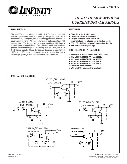
DESCRIPTIONThe SG2800 series integrates eight NPN Darlington pairs with internal suppression diodes to drive lamps, relays, and solenoids in many military, aerospace, and industrial applications that require severe environments. All units feature open collector outputs with greater than 50V breakdown voltages combined with 500mA current carrying capabilities. Five different input configurations provide optimized designs for interfacing with DTL, TTL, PMOS, or CMOS drive signals. These devices are designed to operate from -55°C to 125°C ambient temperature in a 18-pin dual in-line ceramic (J) package and 20-pin leadless chip carrier (LCC).FEATURES•Eight NPN Darlington pairs•Collector currents to 600mA•Output voltages from 50V to 95V•Internal clamping diodes for inductive loads •DTL, TTL, PMOS, or CMOS compatible inputs •Hermetic ceramic packageHIGH RELIABILITY FEATURES♦Available to MIL-STD-883 and DESC SMD♦MIL-M38510/14106BVA - JAN2801J♦MIL-M38510/14107BVA - JAN2802J♦MIL-M38510/14108BVA - JAN2803J♦MIL-M38510/14109BVA - JAN2804J♦Radiation data available♦LMI level "S" processing availableHIGH VOLTAGE MEDIUM CURRENT DRIVER ARRAYSPARTIAL SCHEMATICSABSOLUTE MAXIMUM RATINGS (Note 1)Continuous Collector Current, I C(SG2800, 2820) ......................................................(SG2810) ...............................................................Operating Junction TemperatureHermetic (J, L Packages) .........................................Plastic (N Package) ..................................................Storage Temperature Range ..........................Lead Temperature (Soldering 10 sec.) .........................Output Voltage, V CE(SG2800, 2810 series) ................................................(SG2820 series) ..........................................................Input Voltage, V IN(SG2802,3,4 series) ....................................................Continuous Input Current, I IN ........................................50V 95V 30V 25mA500mA 600mA 150°C 150°C -65°C to 150°C 300°CNote 1. Values beyond which damage may occur.J Package:Thermal Resistance-Junction to Case , θJC .................. 25°C/W Thermal Resistance-Junction to Ambient , θJA ...............70°C/W N Package:Thermal Resistance-Junction to Case , θJC .................. 30°C/W Thermal Resistance-Junction to Ambient , θJA .............. 60°C/W L Package:Thermal Resistance-Junction to Case , θJC .................. 35°C/W Thermal Resistance-Junction to Ambient , θJA .............120°C/WTHERMAL DATANote A.Junction Temperature Calculation: T J = T A + (P D x θJA ).Note B.The above numbers for θJC are maximums for the limitingthermal resistance of the package in a standard mount-ing configuration. The θJA numbers are meant to be guidelines for the thermal performance of the device/pc-board system. All of the above assume no ambient airflow.Output Voltage, V CESG2800, SG2820 series ..............................................SG2810 series .............................................................50V 95VPeak Collector Current, I CSG2800, SG2820 series .........................................SG2810 series ........................................................Operating Ambient Temperature Range ........350mA 500mA -55°C to 125°CNote 2. Range over which the device is functional.RECOMMENDED OPERATING CONDITIONS (Note 2)SELECTION GUIDEDevice V CE Max I C Max Logic Inputs SG280150V 500mA General Purpose PMOS, CMOS SG280250V 500mA 14V-25V PMOS SG280350V 500mA 5V TTL, CMOSSG280450V 500mA 6V-15V CMOS, PMOS SG281150V 600mA General Purpose PMOS, CMOS SG281250V600mA14V-25V PMOSDevice V CE Max I C Max Logic Inputs SG281350V 600mA 5V TTL, CMOSSG281450V 600mA 6V-15V CMOS, PMOS SG281550V 600mA High Output TTL SG282195V 500mA General Purpose PMOS, CMOS SG282395V 500mA 5V TTL, CMOSSG282495V500mA6V-15V CMOS, PMOSCHARACTERISTIC CURVESFIGURE 4.INPUT CHARACTERISTICS - SG2802FIGURE 5.INPUT CHARACTERISTICS - SG2803FIGURE 6.INPUT CHARACTERISTICS - SG2804FIGURE 7.PEAK COLLECTOR CURRENT VS. DUTY CYCLEFIGURE 1.OUTPUT CHARACTERISTICS FIGURE 2.OUTPUT CURRENT VS. INPUT VOLTAGE FIGURE 3.OUTPUT CURRENT VS. INPUT CURRENTNote 1. Contact factory for JAN and DESC product availability.2. All parts are viewed from the top.3. See Selection Guide for specific device types.CONNECTION DIAGRAMS & ORDERING INFORMATION (See Notes Below)AmbientTemperature Range Part No. (Note 3)PackageConnection Diagram18-PIN CERAMIC DIP J - PACKAGESG28XXJ/883B -55°C to 125°C JAN2801J -55°C to 125°C JAN2802J -55°C to 125°C JAN2803J -55°C to 125°C JAN2804J-55°C to 125°C SG2803J/DESC -55°C to 125°C SG2821J/DESC -55°C to 125°C SG2823J/DESC -55°C to 125°C SG2824J/DESC -55°C to 125°C SG28XXJ-55°C to 125°C18-PIN PLASTIC DIP N- PACKAGESG2803N 0°C to 70°C SG2823N 0°C to 70°C 20-PIN CERAMICLEADLESS CHIP CARRIER L- PACKAGESG28XXL/883B -55°C to 125°C SG2803L/DESC -55°C to 125°C SG2821L/DESC -55°C to 125°C SG2823L/DESC -55°C to 125°C SG2824L/DESC -55°C to 125°C SG28XXL-55°C to 125°C1849319201214151716876513121110176543281110121314151716918。
AT24c02最全的中文资料

CA T24C 161/162(16K),CAT24C081 /082(8K) CAT24C041/042(4K),CAT24C021/022(2K)I2C串行CMOS E2PROM,精确的复位控制器和看门狗定时器控制电路特性•数据线上的看门狗定时器(仅对CA T24Cxxl)籲可编程复位门槛电平籲高数据传送速率为400KHz和I2C总线兼容• 2.7V至6V的工作电压•低功耗CMOS工艺籲16字节页写缓冲区籲片内防误擦除写保护籲高低电平复位信号输出——精确的电源电压监视器——可选择5V、3.3V和3V的复位门槛电平•100万次擦写周期•数据保存可长达100年•8脚DIP或SOIC封装•商业级、工业级和汽车温度范围概述CA T24Cxxx是集E2PROM存储器,复位微控制器和看门狗定时器三种流行功能与一体的芯片。
CAT24C161/162 (16K),CAT24C081/082 (8K),CA T24C041/042 (4K)和CAT24C021/022 (2K)以I2C是串行CMOS E2PROM器件。
釆用CMOS工艺大降低了器件的功耗。
CA T24Cxxx 另一特点是16字节的页写缓冲区,提供8脚DIP和SOIC 封装。
CA T24Cxxx的复位功能和看门狗定时器功能保证系统出现故障的时候能给CPU —个复位信号。
CA T24Cxxx 的2脚输出低电平复位信号,7脚输出高电平复位信号。
CAT24Cxxl看狗溢出信号从SDA脚输出。
CAT24Cxx2不具备看门狗功能。
绝对最大参数工作温度:-55°C〜125°C贮存温度:-65°C〜15°C各管脚承受对地电压:-2.0V〜Vcc+2.0V VCC对地电压范围:-2.0V〜7.0V 最大功耗: 1.0W管脚焊接温度(10S): 300 °C输出短路电流:100mA管脚配置]V C C ]RESET方框图表一直流操作特性表二上电时序管脚介绍WP:写保护将该管脚接Vcc,E2PRON就实现写保护(只读)。
MAX247中文资料
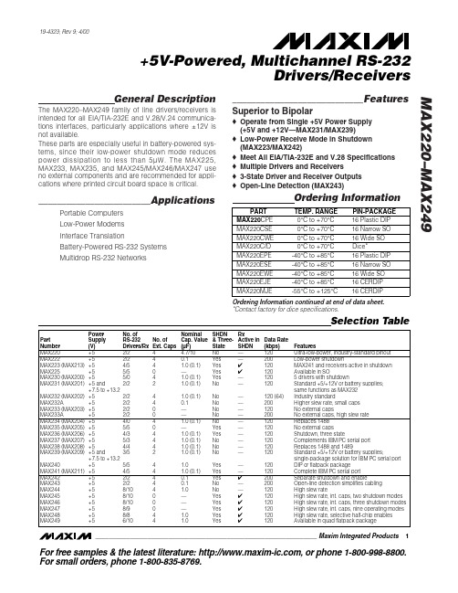
General DescriptionThe MAX220–MAX249 family of line drivers/receivers is intended for all EIA/TIA-232E and V.28/V.24 communica-tions interfaces, particularly applications where ±12V is not available.These parts are especially useful in battery-powered sys-tems, since their low-power shutdown mode reduces power dissipation to less than 5µW. The MAX225,MAX233, MAX235, and MAX245/MAX246/MAX247 use no external components and are recommended for appli-cations where printed circuit board space is critical.________________________ApplicationsPortable Computers Low-Power Modems Interface TranslationBattery-Powered RS-232 Systems Multidrop RS-232 Networks____________________________Features Superior to Bipolaro Operate from Single +5V Power Supply (+5V and +12V—MAX231/MAX239)o Low-Power Receive Mode in Shutdown (MAX223/MAX242)o Meet All EIA/TIA-232E and V.28 Specifications o Multiple Drivers and Receiverso 3-State Driver and Receiver Outputs o Open-Line Detection (MAX243)Ordering InformationOrdering Information continued at end of data sheet.*Contact factory for dice specifications.MAX220–MAX249+5V-Powered, Multichannel RS-232Drivers/Receivers________________________________________________________________Maxim Integrated Products 1Selection Table19-4323; Rev 9; 4/00Power No. of NominalSHDN RxPart Supply RS-232No. of Cap. Value & Three-Active in Data Rate Number (V)Drivers/Rx Ext. Caps (µF)State SHDN (kbps)FeaturesMAX220+52/24 4.7/10No —120Ultra-low-power, industry-standard pinout MAX222+52/2 4 0.1Yes —200Low-power shutdownMAX223 (MAX213)+54/54 1.0 (0.1)Yes ✔120MAX241 and receivers active in shutdown MAX225+55/50—Yes ✔120Available in SOMAX230 (MAX200)+55/04 1.0 (0.1)Yes —120 5 drivers with shutdownMAX231 (MAX201)+5 and2/2 2 1.0 (0.1)No —120Standard +5/+12V or battery supplies; +7.5 to +13.2same functions as MAX232MAX232 (MAX202)+52/24 1.0 (0.1)No —120 (64)Industry standardMAX232A+52/240.1No —200Higher slew rate, small caps MAX233 (MAX203)+52/20— No —120No external capsMAX233A+52/20—No —200No external caps, high slew rate MAX234 (MAX204)+54/04 1.0 (0.1)No —120Replaces 1488MAX235 (MAX205)+55/50—Yes —120No external capsMAX236 (MAX206)+54/34 1.0 (0.1)Yes —120Shutdown, three stateMAX237 (MAX207)+55/34 1.0 (0.1)No —120Complements IBM PC serial port MAX238 (MAX208)+54/44 1.0 (0.1)No —120Replaces 1488 and 1489MAX239 (MAX209)+5 and3/52 1.0 (0.1)No —120Standard +5/+12V or battery supplies;+7.5 to +13.2single-package solution for IBM PC serial port MAX240+55/54 1.0Yes —120DIP or flatpack package MAX241 (MAX211)+54/54 1.0 (0.1)Yes —120Complete IBM PC serial port MAX242+52/240.1Yes ✔200Separate shutdown and enableMAX243+52/240.1No —200Open-line detection simplifies cabling MAX244+58/104 1.0No —120High slew rateMAX245+58/100—Yes ✔120High slew rate, int. caps, two shutdown modes MAX246+58/100—Yes ✔120High slew rate, int. caps, three shutdown modes MAX247+58/90—Yes ✔120High slew rate, int. caps, nine operating modes MAX248+58/84 1.0Yes ✔120High slew rate, selective half-chip enables MAX249+56/1041.0Yes✔120Available in quad flatpack packageFor free samples & the latest literature: , or phone 1-800-998-8800.For small orders, phone 1-800-835-8769.M A X 220–M A X 249+5V-Powered, Multichannel RS-232Drivers/ReceiversABSOLUTE MAXIMUM RATINGS—MAX220/222/232A/233A/242/243ELECTRICAL CHARACTERISTICS—MAX220/222/232A/233A/242/243(V CC = +5V ±10%, C1–C4 = 0.1µF‚ MAX220, C1 = 0.047µF, C2–C4 = 0.33µF, T A = T MIN to T MAX ‚ unless otherwise noted.)Note 1:Input voltage measured with T OUT in high-impedance state, SHDN or V CC = 0V.Note 2:For the MAX220, V+ and V- can have a maximum magnitude of 7V, but their absolute difference cannot exceed 13V.Stresses beyond those listed under “Absolute Maximum Ratings” may cause permanent damage to the device. These are stress ratings only, and functional operation of the device at these or any other conditions beyond those indicated in the operational sections of the specifications is not implied. Exposure to absolute maximum rating conditions for extended periods may affect device reliability.Supply Voltage (V CC )...............................................-0.3V to +6V Input VoltagesT IN ..............................................................-0.3V to (V CC - 0.3V)R IN (Except MAX220)........................................................±30V R IN (MAX220).....................................................................±25V T OUT (Except MAX220) (Note 1).......................................±15V T OUT (MAX220)...............................................................±13.2V Output VoltagesT OUT ...................................................................................±15V R OUT .........................................................-0.3V to (V CC + 0.3V)Driver/Receiver Output Short Circuited to GND.........Continuous Continuous Power Dissipation (T A = +70°C)16-Pin Plastic DIP (derate 10.53mW/°C above +70°C)....842mW 18-Pin Plastic DIP (derate 11.11mW/°C above +70°C)....889mW20-Pin Plastic DIP (derate 8.00mW/°C above +70°C)..440mW 16-Pin Narrow SO (derate 8.70mW/°C above +70°C)...696mW 16-Pin Wide SO (derate 9.52mW/°C above +70°C)......762mW 18-Pin Wide SO (derate 9.52mW/°C above +70°C)......762mW 20-Pin Wide SO (derate 10.00mW/°C above +70°C)....800mW 20-Pin SSOP (derate 8.00mW/°C above +70°C)..........640mW 16-Pin CERDIP (derate 10.00mW/°C above +70°C).....800mW 18-Pin CERDIP (derate 10.53mW/°C above +70°C).....842mW Operating Temperature RangesMAX2_ _AC_ _, MAX2_ _C_ _.............................0°C to +70°C MAX2_ _AE_ _, MAX2_ _E_ _..........................-40°C to +85°C MAX2_ _AM_ _, MAX2_ _M_ _.......................-55°C to +125°C Storage Temperature Range.............................-65°C to +160°C Lead Temperature (soldering, 10sec).............................+300°CMAX220–MAX249+5V-Powered, Multichannel RS-232Drivers/Receivers_______________________________________________________________________________________3Note 3:MAX243 R2OUT is guaranteed to be low when R2IN is ≥0V or is floating.ELECTRICAL CHARACTERISTICS—MAX220/222/232A/233A/242/243 (continued)(V= +5V ±10%, C1–C4 = 0.1µF‚ MAX220, C1 = 0.047µF, C2–C4 = 0.33µF, T = T to T ‚ unless otherwise noted.)M A X 220–M A X 249+5V-Powered, Multichannel RS-232Drivers/Receivers 4_________________________________________________________________________________________________________________________________Typical Operating CharacteristicsMAX220/MAX222/MAX232A/MAX233A/MAX242/MAX243108-1051525OUTPUT VOLTAGE vs. LOAD CURRENT-4-6-8-2642LOAD CURRENT (mA)O U T P U T V O L T A G E (V )1002011104104060AVAILABLE OUTPUT CURRENTvs. DATA RATE65798DATA RATE (kbits/sec)O U T P U T C U R R E N T (m A )203050+10V-10VMAX222/MAX242ON-TIME EXITING SHUTDOWN+5V +5V 0V0V 500µs/div V +, V - V O L T A G E (V )MAX220–MAX249+5V-Powered, Multichannel RS-232Drivers/Receivers_______________________________________________________________________________________5V CC ...........................................................................-0.3V to +6V V+................................................................(V CC - 0.3V) to +14V V-............................................................................+0.3V to -14V Input VoltagesT IN ............................................................-0.3V to (V CC + 0.3V)R IN ......................................................................................±30V Output VoltagesT OUT ...................................................(V+ + 0.3V) to (V- - 0.3V)R OUT .........................................................-0.3V to (V CC + 0.3V)Short-Circuit Duration, T OUT ......................................Continuous Continuous Power Dissipation (T A = +70°C)14-Pin Plastic DIP (derate 10.00mW/°C above +70°C)....800mW 16-Pin Plastic DIP (derate 10.53mW/°C above +70°C)....842mW 20-Pin Plastic DIP (derate 11.11mW/°C above +70°C)....889mW 24-Pin Narrow Plastic DIP(derate 13.33mW/°C above +70°C)..........1.07W24-Pin Plastic DIP (derate 9.09mW/°C above +70°C)......500mW 16-Pin Wide SO (derate 9.52mW/°C above +70°C).........762mW20-Pin Wide SO (derate 10 00mW/°C above +70°C).......800mW 24-Pin Wide SO (derate 11.76mW/°C above +70°C).......941mW 28-Pin Wide SO (derate 12.50mW/°C above +70°C) .............1W 44-Pin Plastic FP (derate 11.11mW/°C above +70°C).....889mW 14-Pin CERDIP (derate 9.09mW/°C above +70°C)..........727mW 16-Pin CERDIP (derate 10.00mW/°C above +70°C)........800mW 20-Pin CERDIP (derate 11.11mW/°C above +70°C)........889mW 24-Pin Narrow CERDIP(derate 12.50mW/°C above +70°C)..............1W24-Pin Sidebraze (derate 20.0mW/°C above +70°C)..........1.6W 28-Pin SSOP (derate 9.52mW/°C above +70°C).............762mW Operating Temperature RangesMAX2 _ _ C _ _......................................................0°C to +70°C MAX2 _ _ E _ _...................................................-40°C to +85°C MAX2 _ _ M _ _ ...............................................-55°C to +125°C Storage Temperature Range.............................-65°C to +160°C Lead Temperature (soldering, 10sec).............................+300°CABSOLUTE MAXIMUM RATINGS—MAX223/MAX230–MAX241ELECTRICAL CHARACTERISTICS—MAX223/MAX230–MAX241(MAX223/230/232/234/236/237/238/240/241, V CC = +5V ±10; MAX233/MAX235, V CC = 5V ±5%‚ C1–C4 = 1.0µF; MAX231/MAX239,V CC = 5V ±10%; V+ = 7.5V to 13.2V; T A = T MIN to T MAX ; unless otherwise noted.)Stresses beyond those listed under “Absolute Maximum Ratings” may cause permanent damage to the device. These are stress ratings only, and functional operation of the device at these or any other conditions beyond those indicated in the operational sections of the specifications is not implied. Exposure to absolute maximum rating conditions for extended periods may affect device reliability.M A X 220–M A X 249+5V-Powered, Multichannel RS-232Drivers/Receivers 6_______________________________________________________________________________________ELECTRICAL CHARACTERISTICS—MAX223/MAX230–MAX241 (continued)(MAX223/230/232/234/236/237/238/240/241, V CC = +5V ±10; MAX233/MAX235, V CC = 5V ±5%‚ C1–C4 = 1.0µF; MAX231/MAX239,V CC = 5V ±10%; V+ = 7.5V to 13.2V; T A = T MIN to T MAX ; unless otherwise noted.)MAX220–MAX249+5V-Powered, Multichannel RS-232Drivers/Receivers_______________________________________________________________________________________78.56.54.55.5TRANSMITTER OUTPUT VOLTAGE (V OH ) vs. V CC7.08.0V CC (V)V O H (V )5.07.57.46.02500TRANSMITTER OUTPUT VOLTAGE (V OH )vs. LOAD CAPACITANCE AT DIFFERENT DATA RATES6.46.27.27.0LOAD CAPACITANCE (pF)V O H (V )1500100050020006.86.612.04.02500TRANSMITTER SLEW RATE vs. LOAD CAPACITANCE6.05.011.09.010.0LOAD CAPACITANCE (pF)S L E W R A T E (V /µs )1500100050020008.07.0-6.0-9.04.55.5TRANSMITTER OUTPUT VOLTAGE (V OL ) vs. V CC-8.0-8.5-6.5-7.0V CC (V)V O L (V )5.0-7.5-6.0-7.62500TRANSMITTER OUTPUT VOLTAGE (V OL )vs. LOAD CAPACITANCE AT DIFFERENT DATA RATES-7.0-7.2-7.4-6.2-6.4LOAD CAPACITANCE (pF)V O L (V )150010005002000-6.6-6.810-105101520253035404550TRANSMITTER OUTPUT VOLTAGE (V+, V-)vs. LOAD CURRENT-2-6-4-886CURRENT (mA)V +, V - (V )420__________________________________________Typical Operating CharacteristicsMAX223/MAX230–MAX241*SHUTDOWN POLARITY IS REVERSED FOR NON MAX241 PARTSV+, V- WHEN EXITING SHUTDOWN(1µF CAPACITORS)MAX220-13SHDN*V-O V+500ms/divM A X 220–M A X 249+5V-Powered, Multichannel RS-232Drivers/Receivers 8_______________________________________________________________________________________ABSOLUTE MAXIMUM RATINGS—MAX225/MAX244–MAX249ELECTRICAL CHARACTERISTICS—MAX225/MAX244–MAX249(MAX225, V CC = 5.0V ±5%; MAX244–MAX249, V CC = +5.0V ±10%, external capacitors C1–C4 = 1µF; T A = T MIN to T MAX ; unless oth-erwise noted.)Note 4:Input voltage measured with transmitter output in a high-impedance state, shutdown, or V CC = 0V.Stresses beyond those listed under “Absolute Maximum Ratings” may cause permanent damage to the device. These are stress ratings only, and functional operation of the device at these or any other conditions beyond those indicated in the operational sections of the specifications is not implied. Exposure to absolute maximum rating conditions for extended periods may affect device reliability.Supply Voltage (V CC )...............................................-0.3V to +6V Input VoltagesT IN ‚ ENA , ENB , ENR , ENT , ENRA ,ENRB , ENTA , ENTB ..................................-0.3V to (V CC + 0.3V)R IN .....................................................................................±25V T OUT (Note 3).....................................................................±15V R OUT ........................................................-0.3V to (V CC + 0.3V)Short Circuit (one output at a time)T OUT to GND............................................................Continuous R OUT to GND............................................................ContinuousContinuous Power Dissipation (T A = +70°C)28-Pin Wide SO (derate 12.50mW/°C above +70°C).............1W 40-Pin Plastic DIP (derate 11.11mW/°C above +70°C)...611mW 44-Pin PLCC (derate 13.33mW/°C above +70°C)...........1.07W Operating Temperature RangesMAX225C_ _, MAX24_C_ _ ..................................0°C to +70°C MAX225E_ _, MAX24_E_ _ ...............................-40°C to +85°C Storage Temperature Range.............................-65°C to +160°C Lead Temperature (soldering,10sec)..............................+300°CMAX220–MAX249+5V-Powered, Multichannel RS-232Drivers/Receivers_______________________________________________________________________________________9Note 5:The 300Ωminimum specification complies with EIA/TIA-232E, but the actual resistance when in shutdown mode or V CC =0V is 10M Ωas is implied by the leakage specification.ELECTRICAL CHARACTERISTICS—MAX225/MAX244–MAX249 (continued)(MAX225, V CC = 5.0V ±5%; MAX244–MAX249, V CC = +5.0V ±10%, external capacitors C1–C4 = 1µF; T A = T MIN to T MAX ; unless oth-erwise noted.)M A X 220–M A X 249+5V-Powered, Multichannel RS-232Drivers/Receivers 10________________________________________________________________________________________________________________________________Typical Operating CharacteristicsMAX225/MAX244–MAX24918212345TRANSMITTER SLEW RATE vs. LOAD CAPACITANCE86416LOAD CAPACITANCE (nF)T R A N S M I T T E R S L E W R A T E (V /µs )14121010-105101520253035OUTPUT VOLTAGEvs. LOAD CURRENT FOR V+ AND V--2-4-6-88LOAD CURRENT (mA)O U T P U T V O L T A G E (V )64209.05.012345TRANSMITTER OUTPUT VOLTAGE (V+, V-)vs. LOAD CAPACITANCE AT DIFFERENT DATA RATES6.05.58.5LOAD CAPACITANCE (nF)V +, V (V )8.07.57.06.5MAX220–MAX249Drivers/Receivers______________________________________________________________________________________11Figure 1. Transmitter Propagation-Delay Timing Figure 2. Receiver Propagation-Delay TimingFigure 3. Receiver-Output Enable and Disable Timing Figure 4. Transmitter-Output Disable TimingM A X 220–M A X 249Drivers/Receivers 12______________________________________________________________________________________ENT ENR OPERATION STATUS TRANSMITTERSRECEIVERS00Normal Operation All Active All Active 01Normal Operation All Active All 3-State10Shutdown All 3-State All Low-Power Receive Mode 11ShutdownAll 3-StateAll 3-StateTable 1a. MAX245 Control Pin ConfigurationsENT ENR OPERATION STATUS TRANSMITTERS RECEIVERSTA1–TA4TB1–TB4RA1–RA5RB1–RB500Normal Operation All Active All Active All Active All Active 01Normal Operation All Active All Active RA1–RA4 3-State,RA5 Active RB1–RB4 3-State,RB5 Active 1ShutdownAll 3-StateAll 3-StateAll Low-Power Receive Mode All Low-Power Receive Mode 11Shutdown All 3-State All 3-StateRA1–RA4 3-State,RA5 Low-Power Receive ModeRB1–RB4 3-State,RB5 Low-Power Receive ModeTable 1b. MAX245 Control Pin ConfigurationsTable 1c. MAX246 Control Pin ConfigurationsENA ENB OPERATION STATUS TRANSMITTERS RECEIVERSTA1–TA4TB1–TB4RA1–RA5RB1–RB500Normal Operation All Active All Active All Active All Active 01Normal Operation All Active All 3-State All Active RB1–RB4 3-State,RB5 Active 1ShutdownAll 3-StateAll ActiveRA1–RA4 3-State,RA5 Active All Active 11Shutdown All 3-State All 3-StateRA1–RA4 3-State,RA5 Low-Power Receive ModeRB1–RB4 3-State,RA5 Low-Power Receive ModeMAX220–MAX249Drivers/Receivers______________________________________________________________________________________13Table 1d. MAX247/MAX248/MAX249 Control Pin ConfigurationsM A X 220–M A X 249_______________Detailed DescriptionThe MAX220–MAX249 contain four sections: dual charge-pump DC-DC voltage converters, RS-232 dri-vers, RS-232 receivers, and receiver and transmitter enable control inputs.Dual Charge-Pump Voltage ConverterThe MAX220–MAX249 have two internal charge-pumps that convert +5V to ±10V (unloaded) for RS-232 driver operation. The first converter uses capacitor C1 to dou-ble the +5V input to +10V on C3 at the V+ output. The second converter uses capacitor C2 to invert +10V to -10V on C4 at the V- output.A small amount of power may be drawn from the +10V (V+) and -10V (V-) outputs to power external circuitry (see the Typical Operating Characteristics section),except on the MAX225 and MAX245–MAX247, where these pins are not available. V+ and V- are not regulated,so the output voltage drops with increasing load current.Do not load V+ and V- to a point that violates the mini-mum ±5V EIA/TIA-232E driver output voltage when sourcing current from V+ and V- to external circuitry. When using the shutdown feature in the MAX222,MAX225, MAX230, MAX235, MAX236, MAX240,MAX241, and MAX245–MAX249, avoid using V+ and V-to power external circuitry. When these parts are shut down, V- falls to 0V, and V+ falls to +5V. For applica-tions where a +10V external supply is applied to the V+pin (instead of using the internal charge pump to gen-erate +10V), the C1 capacitor must not be installed and the SHDN pin must be tied to V CC . This is because V+is internally connected to V CC in shutdown mode.RS-232 DriversThe typical driver output voltage swing is ±8V when loaded with a nominal 5k ΩRS-232 receiver and V CC =+5V. Output swing is guaranteed to meet the EIA/TIA-232E and V.28 specification, which calls for ±5V mini-mum driver output levels under worst-case conditions.These include a minimum 3k Ωload, V CC = +4.5V, and maximum operating temperature. Unloaded driver out-put voltage ranges from (V+ -1.3V) to (V- +0.5V). Input thresholds are both TTL and CMOS compatible.The inputs of unused drivers can be left unconnected since 400k Ωinput pull-up resistors to V CC are built in (except for the MAX220). The pull-up resistors force the outputs of unused drivers low because all drivers invert.The internal input pull-up resistors typically source 12µA,except in shutdown mode where the pull-ups are dis-abled. Driver outputs turn off and enter a high-imped-ance state—where leakage current is typically microamperes (maximum 25µA)—when in shutdownmode, in three-state mode, or when device power is removed. Outputs can be driven to ±15V. The power-supply current typically drops to 8µA in shutdown mode.The MAX220 does not have pull-up resistors to force the ouputs of the unused drivers low. Connect unused inputs to GND or V CC .The MAX239 has a receiver three-state control line, and the MAX223, MAX225, MAX235, MAX236, MAX240,and MAX241 have both a receiver three-state control line and a low-power shutdown control. Table 2 shows the effects of the shutdown control and receiver three-state control on the receiver outputs.The receiver TTL/CMOS outputs are in a high-imped-ance, three-state mode whenever the three-state enable line is high (for the MAX225/MAX235/MAX236/MAX239–MAX241), and are also high-impedance whenever the shutdown control line is high.When in low-power shutdown mode, the driver outputs are turned off and their leakage current is less than 1µA with the driver output pulled to ground. The driver output leakage remains less than 1µA, even if the transmitter output is backdriven between 0V and (V CC + 6V). Below -0.5V, the transmitter is diode clamped to ground with 1k Ωseries impedance. The transmitter is also zener clamped to approximately V CC + 6V, with a series impedance of 1k Ω.The driver output slew rate is limited to less than 30V/µs as required by the EIA/TIA-232E and V.28 specifica-tions. Typical slew rates are 24V/µs unloaded and 10V/µs loaded with 3Ωand 2500pF.RS-232 ReceiversEIA/TIA-232E and V.28 specifications define a voltage level greater than 3V as a logic 0, so all receivers invert.Input thresholds are set at 0.8V and 2.4V, so receivers respond to TTL level inputs as well as EIA/TIA-232E and V.28 levels.The receiver inputs withstand an input overvoltage up to ±25V and provide input terminating resistors withDrivers/Receivers 14Table 2. Three-State Control of ReceiversMAX220–MAX249Drivers/Receivers______________________________________________________________________________________15nominal 5k Ωvalues. The receivers implement Type 1interpretation of the fault conditions of V.28 and EIA/TIA-232E.The receiver input hysteresis is typically 0.5V with a guaranteed minimum of 0.2V. This produces clear out-put transitions with slow-moving input signals, even with moderate amounts of noise and ringing. The receiver propagation delay is typically 600ns and is independent of input swing direction.Low-Power Receive ModeThe low-power receive-mode feature of the MAX223,MAX242, and MAX245–MAX249 puts the IC into shut-down mode but still allows it to receive information. This is important for applications where systems are periodi-cally awakened to look for activity. Using low-power receive mode, the system can still receive a signal that will activate it on command and prepare it for communi-cation at faster data rates. This operation conserves system power.Negative Threshold—MAX243The MAX243 is pin compatible with the MAX232A, differ-ing only in that RS-232 cable fault protection is removed on one of the two receiver inputs. This means that control lines such as CTS and RTS can either be driven or left floating without interrupting communication. Different cables are not needed to interface with different pieces of equipment.The input threshold of the receiver without cable fault protection is -0.8V rather than +1.4V. Its output goes positive only if the input is connected to a control line that is actively driven negative. If not driven, it defaults to the 0 or “OK to send” state. Normally‚ the MAX243’s other receiver (+1.4V threshold) is used for the data line (TD or RD)‚ while the negative threshold receiver is con-nected to the control line (DTR‚ DTS‚ CTS‚ RTS, etc.). Other members of the RS-232 family implement the optional cable fault protection as specified by EIA/TIA-232E specifications. This means a receiver output goes high whenever its input is driven negative‚ left floating‚or shorted to ground. The high output tells the serial communications IC to stop sending data. To avoid this‚the control lines must either be driven or connected with jumpers to an appropriate positive voltage level.Shutdown—MAX222–MAX242On the MAX222‚ MAX235‚ MAX236‚ MAX240‚ and MAX241‚ all receivers are disabled during shutdown.On the MAX223 and MAX242‚ two receivers continue to operate in a reduced power mode when the chip is in shutdown. Under these conditions‚ the propagation delay increases to about 2.5µs for a high-to-low input transition. When in shutdown, the receiver acts as a CMOS inverter with no hysteresis. The MAX223 and MAX242 also have a receiver output enable input (EN for the MAX242 and EN for the MAX223) that allows receiver output control independent of SHDN (SHDN for MAX241). With all other devices‚ SHDN (SH DN for MAX241) also disables the receiver outputs.The MAX225 provides five transmitters and five receivers‚ while the MAX245 provides ten receivers and eight transmitters. Both devices have separate receiver and transmitter-enable controls. The charge pumps turn off and the devices shut down when a logic high is applied to the ENT input. In this state, the supply cur-rent drops to less than 25µA and the receivers continue to operate in a low-power receive mode. Driver outputs enter a high-impedance state (three-state mode). On the MAX225‚ all five receivers are controlled by the ENR input. On the MAX245‚ eight of the receiver out-puts are controlled by the ENR input‚ while the remain-ing two receivers (RA5 and RB5) are always active.RA1–RA4 and RB1–RB4 are put in a three-state mode when ENR is a logic high.Receiver and Transmitter EnableControl InputsThe MAX225 and MAX245–MAX249 feature transmitter and receiver enable controls.The receivers have three modes of operation: full-speed receive (normal active)‚ three-state (disabled)‚ and low-power receive (enabled receivers continue to function at lower data rates). The receiver enable inputs control the full-speed receive and three-state modes. The transmitters have two modes of operation: full-speed transmit (normal active) and three-state (disabled). The transmitter enable inputs also control the shutdown mode. The device enters shutdown mode when all transmitters are disabled. Enabled receivers function in the low-power receive mode when in shutdown.M A X 220–M A X 249Tables 1a–1d define the control states. The MAX244has no control pins and is not included in these tables. The MAX246 has ten receivers and eight drivers with two control pins, each controlling one side of the device. A logic high at the A-side control input (ENA )causes the four A-side receivers and drivers to go into a three-state mode. Similarly, the B-side control input (ENB ) causes the four B-side drivers and receivers to go into a three-state mode. As in the MAX245, one A-side and one B-side receiver (RA5 and RB5) remain active at all times. The entire device is put into shut-down mode when both the A and B sides are disabled (ENA = ENB = +5V).The MAX247 provides nine receivers and eight drivers with four control pins. The ENRA and ENRB receiver enable inputs each control four receiver outputs. The ENTA and ENTB transmitter enable inputs each control four drivers. The ninth receiver (RB5) is always active.The device enters shutdown mode with a logic high on both ENTA and ENTB .The MAX248 provides eight receivers and eight drivers with four control pins. The ENRA and ENRB receiver enable inputs each control four receiver outputs. The ENTA and ENTB transmitter enable inputs control four drivers each. This part does not have an always-active receiver. The device enters shutdown mode and trans-mitters go into a three-state mode with a logic high on both ENTA and ENTB .The MAX249 provides ten receivers and six drivers with four control pins. The ENRA and ENRB receiver enable inputs each control five receiver outputs. The ENTA and ENTB transmitter enable inputs control three dri-vers each. There is no always-active receiver. The device enters shutdown mode and transmitters go into a three-state mode with a logic high on both ENTA and ENTB . In shutdown mode, active receivers operate in a low-power receive mode at data rates up to 20kbits/sec.__________Applications InformationFigures 5 through 25 show pin configurations and typi-cal operating circuits. In applications that are sensitive to power-supply noise, V CC should be decoupled to ground with a capacitor of the same value as C1 and C2 connected as close as possible to the device.Drivers/Receivers16______________________________________________________________________________________。
TLV2474资料
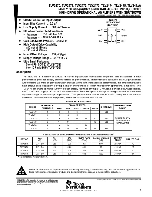
D D D D D D D D D
CMOS Rail-To-Rail Input/Output Input Bias Current . . . 2.5 pA Low Supply Current . . . 600 µA/Channel Ultra-Low Power Shutdown Mode - IDD(SHDN) . . . 350 nA/ch at 3 V - IDD(SHDN) . . . 1000 nA/ch at 5 V Gain-Bandwidth Product . . . 2.8 MHz High Output Drive Capability - ±10 mA at 180 mV - ±35 mA at 500 mV Input Offset Voltage . . . 250 µV (typ) Supply Voltage Range . . . 2.7 V to 6 V Ultra Small Packaging - 5 or 6 Pin SOT-23 (TLV2470/1) - 8 or 10 Pin MSOP (TLV2472/3)
FAMILY PACKAGE TABLE DEVICE TLV2470 TLV2471 TLV2472 TLV2473 TLV2474 TLV2475 NUMBER OF CHANNELS 1 1 2 2 4 4 PACKAGE TYPES PDIP 8 8 8 14 14 16 SOIC 8 8 8 14 14 16 SOT-23 6 5 — — — — TSSOP — — — — 14 16 MSOP — — 8 10 — — SHUTDOWN Yes — — Yes — Yes Refer to the EVM Selection Guide (Lit# SLOU060) UNIVERSAL EVM BOARD
P8SG-1212ZH52中文资料
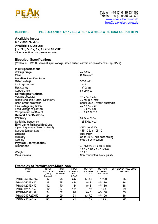
P8SG-XXXXZH52 5.2 KV ISOLATED 1.5 W REGULATED DUAL OUTPUT DIP24
Dimensions
Derating Graph and Pinning
Output
Temperature Derating Graph
Ambient Temperature ° C 71
P8SG-053R6ZH52 P8SG-0505ZH52 P8SG-1205ZH52 P8SG-1212ZH52 P8SG-2405ZH52 P8SG-247R2ZH52 P8SG-2415ZH52
5 5 12 12 24 24 24
78 75 70 67 32 29 26
443 454 184 181 96 91 91
Available Inputs:
5, 12 and 24 VDC
Available Outputs:
(+/-) 3.6, 5, 7.2, 12, 15 and 18 VDC
Other specifications please enquire.
Electrical Specifications
(Typical at + 25° C, nominal input voltage, rated output current unless otherwise specified) Input Specifications Voltage range Filter Isolation Specifications Rated voltage Leakage current Resistance Capacitance Output Specifications Voltage accuracy Ripple and noise (at 20 MHz BW) Short circuit protection Line voltage regulation Load voltage regulation Temperature coefficient General Specifications Efficiency Switching frequency Environmental Specifications Operating temperature (ambient) Storage temperature Derating Humidity Cooling Physical Characteristics Dimensions Weight Case material +/- 10 % Pi Network 5200 Vdc 1 mA 109 Ohm 60 pF typ. +/- 2 %, max. 75 mV p-p, max. Continuous , restart automatic +/- 0,5 % max. +/- 0,5 % max. +/- 0,02 % / °C 65 % to 85 % 125 KHz, typ. -25°C to +71°C - 55 °C to + 125 °C See graph Up to 90 %, non condensing Free air convection 31,75 x 20,32 x 10,16 mm 1,25 x 0,80 x 0,40 inches 12,2 g Non conductive black plastic
2472中文资料
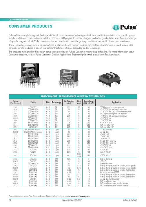
● The ferrite core is a slim EE50-type, leading to a maximum transformer height of 28mm above the PCB
9+9 6+6 6+6 8+8 7+7 9+9 9+9 7+7 11 +11 6+6 6+6
6+6
4+4 6+6 9+9 4+4 5+4 4+4 4+4 5+5 5+5 5+5 5+5 5+5 7+7
Slot Slot Slot Slot Slot Slot Slot Slot Slot Slot
Layer Layer Layer Layer Layer Layer Layer Layer Layer Layer Layer
14"- 90° color TV Set-top Box 14"÷21" - 90° 17"÷21" - 90° 110° Color TV 25"÷29" 110° Color TV 28"÷34" 110° Color TV 14"-15" CTV 90° 25"-29" CTV 110° LCD TV 26" LCD TV 26"-32"
SWITCH-MODE TRANSFORMER GUIDE BY TECHNOLOGY
SMPTE 311M多线缆说明书
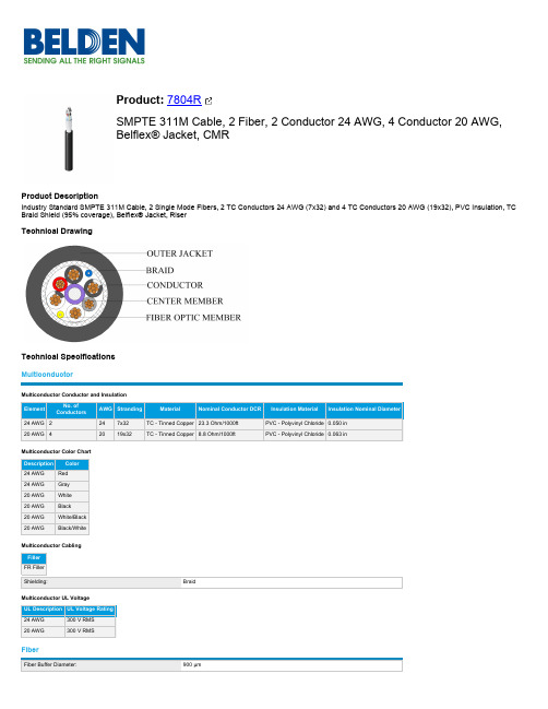
Product:7804RSMPTE 311M Cable, 2 Fiber, 2 Conductor 24 AWG, 4 Conductor 20 AWG,Belflex® Jacket, CMRProduct DescriptionIndustry Standard SMPTE 311M Cable, 2 Single Mode Fibers, 2 TC Conductors 24 AWG (7x32) and 4 TC Conductors 20 AWG (19x32), PVC Insulation, TC Braid Shield (95% coverage), Belflex® Jacket, RiserTechnical DrawingTechnical SpecificationsMulticonductorMulticonductor Conductor and InsulationMulticonductor Color ChartMulticonductor CablingMulticonductor UL VoltageFiberFiber Buffer Material:PVC - Polyvinyl ChlorideFiber Color Coding:Yel, BluFiber Count:2Fiber Type:OS2, G.657.A2Mode Field Diameter:9.2 µmWavelength@Optical SM1:1310 nm, 1550 nmMax Attenuation at 1310 nm:0.5 dB/kmMax Attenuation at 1550 nm:0.5 dB/kmOverall CableOverall ShieldingLayer 1Type Material CoverageOverall Braid TC - Tinned Copper0.95 %Jacket:PVCSeparator Material@OuterJacket1 1:PVC - Polyvinyl ChlorideOperating Temp Range:-40°C to +70°CInstallation Temp Range:-10°C to +70°CStorage Temp Range:-40°C to +70°CMax Recommended Pulling Tension:1350 NBulk Cable Weight:80 lbs/1000ftApplicable Standards & Environmental ProgramsNEC/(UL) Specification:CMRCEC/C(UL) Specification:CMGEU Directive 2011/65/EU (ROHS II):YesEU Directive 2015/863/EU:YesEU Directive 2000/53/EC (ELV):YesEU Directive 2012/19/EU (WEEE):YesEU Directive 2003/11/EC (BFR):YesOther Specification:SMPTE 311SuitabilitySuitability - Indoor:YesFlame TestUL Flammability:UL1666 Vertical ShaftC(UL) Flammability:FT4Plenum/Non-PlenumPlenum (Y/N):NPlenum Number:7804POverall Armor ShieldVariantsItem #Color UPC Length Footnote7804R B59CUT Black, Matte6128251895037804R B591000Matte Black6128253786481,000 ft C7804R B591640Matte Black6128251894801,640 ft C7804R B593280Matte Black6128251894973,280 ft C7804R B59500Matte Black612825378655500 ft CUpdate and Revision:Revision Number: 0.167 Revision Date: 01-31-2020© 2020 Belden, IncAll Rights Reserved.Although Belden makes every reasonable effort to ensure their accuracy at the time of this publication, information and specifications described here in are subject to error or omission and to change without notice, and the listing of such information and specifications does not ensure product availability.Belden provides the information and specifications herein on an "ASIS" basis, with no representations or warranties, whether express, statutory or implied. In no event will Belden be liable for any damages (including consequential, indirect, incidental, special, punitive, or exemplary damages) whatsoever, even if Belden has been advised of the possibility of such damages, whether in an action under contract, negligence or any other theory, arising out of or in connection with the use, or inability to use, the information or specifications described herein.All sales of Belden products are subject to Belden's standard terms and conditions of sale.Belden believes this product to be in compliance with all applicable environmental programs as listed in the data sheet. The information provided is correct to the best of Belden's knowledge, information and belief at the date of its publication. This information is designed only as a general guide for the safe handling, storage, and any other operation of the product itself or the one that it becomes a part of. The Product Disclosure is not to be considered a warranty or quality specification. Regulatory information is for guidance purposes only. Product users are responsible for determining the applicability of legislation and regulations based on their individual usage of the product.。
NETGEAR ProSafe 24-和48-port Gigabit企业级类L2管理交换机数据表说
WG302ProSafe 802.11g Wireless Access Point350 E. Plumeria DriveSan Jose, CA 95134-1911 USA 1-888-NETGEAR (638-4327)E-mail: info@ –System memory: 128 MB –Packet buffer memory:GSM7224v2: max support 0.75 MB buffer memoryGSM7248v2: max support 1.5 MB buffer memory–Code storage (flash): 32 MB–Address database size: 8 K media access control (MAC) addresses –Number of VLANs: 1024 (1-4093) –Number of trunks: 64 –Number of queues: 8–Number of static route: 32 –Number of routed VLANs: 32 –Number of ARP entries: 480 –Number of ACL rules: 224–Jumbo frame support: up to 9 K packet size–Acoustic noise:GSM7224v2: 38.6 dB GSM7248v2: 48.8 dB –Heat dissipation:GSM7224v2: 131.439 BTU/hr GSM7248v2: 244.101 BTU/hr–Mean time between failures (MTBF): GSM7224v2: 239,032 hours(~27 years) GSM7248v2: 162,303 hours (~19 years)• User Interfaces–Command Line Interface (CLI) via console port (5 sessions)–Web-based management viaembedded HTTP server protected with Secure Sockets Layer–(SSLv3) or Transport Layer Security (TLS v1)–Telnet remote login (5 sessions) securable with Secure Shell (SSH v1.5, v2)• LEDs–Per port: Speed, link, activityPer device: Power, fan, RPS status • Network Standards Compatibility –IEEE 802.3i 10BASE-T–IEEE 802.3u 100BASE-TX, 100BASE-FX –IEEE 802.3ab 1000BASE-T –IEEE 802.3z 1000BASE-X –IEEE 802.3x flow control• Physical Specifications –Dimensions (w x d x h): 440 x 205 x 43 mm (17.3 x 8.1 x 1.6 in) –Weight:GSM7224v2: 3.65 kg (8.03 lb) GSM7248v2: 4.15 kg (9.13 lb)• Environmental Specifications–Operating temperature: 0° to 55° C (32° to 131° F)–Storage temperature: -20° to 70° C (-4° to 158° F)–Operating humidity: 90% maximum relative humidity, non-condensing –Storage humidity: 95% maximum relative humidity, non-condensing –Operating altitude: 3,000 m (10,000 ft) maximum–Storage altitude: 3,000 m (10,000 ft) maximum • Electrical Specifications –Power consumption:GSM7224v2 38.5W maximum GSM7248v2 71.5W maximum –Redundant power supply input: 12V • Electromagnetic Emissions –CE mark–EN 55022 Class A - Emissions –EN 55024 - Immunity –FCC Part 15 Class A –VCCI Class A –C-Tick• Electromagnetic Safety –CE mark –EN 60950-1 –UL/cUL 60950-1Warranty–NETGEAR Lifetime Warranty †Modules–ProSafe AGM731F 1000BASE-SX SFP GBIC–ProSafe AGM732F 1000BASE-LX SFP GBIC–ProSafe AGM733 1000BASE-ZX SFP GBIC–100FX SFP LC transceiverPackage Contents–ProSafe Gigabit L2 Managed Switch (GSM7224v2 or GSM7248v2) –Null modem cable –Rubber footpads –Power cable –Rack-mount kit –Installation guide –Resource CD-ROM–Warranty/support information cardOrdering Information• North America–GSM7224-200NAS –GSM7248-200NAS • Europe–GSM7224-200EUS –GSM7248-200EUS • Asia–GSM7224-200AJS –GSM7248-200AJSProSupport Service Packs Available GSM7224v2• O nCall 24x7, Category 2 –PMB0332• X PressHW , Category 2 –PRR0332-100GSM7248v2• O nCall 24x7, Category 3 –PMB0333• X PressHW , Category 3 –PRR0333-100© 2009 NETGEAR, Inc. NETGEAR, the NETGEAR Logo, NETGEAR Digital Entertainer Logo, Connect with Innovation, FrontView, IntelliFi, PowerShift, ProSafe, ProSecure, RAIDar, RAIDiator, RangeMax, ReadyNAS, Smart Wizard, X-RAID, and X-RAID2, are trademarks and/or reg-istered trademarks of NETGEAR, Inc. and/or subsidiaries in the United States and/or other countries. Mac and the Mac logo are trademarks of Apple Inc., registered in the U.S. and other countries. Other brand names mentioned herein are for identification purposes only and may be trademarks of their respective holder(s). Information is subject to change without notice. All rights reserved.*Basic technical support provided for 90 days from date of purchase.†Lifetime warranty for product purchased after 05/01/2007. For product purchased before 05/01/2007, warranty is 5 years.D-GSM7224v2/GSM7248v2-1。
介绍几种光电传感器

50
—
—
—
900 ±15
—
—
< 50 高电平 H →L 0. 3
L →H 6 H →L 2
900 ±15 250
50
< 50 高电平 L →H 0. 3
L →H 2 H →L 6
900 ±15 250
50
© 1994-2008 China Academic Journal Electronic Publishing House. All rights reserved.
图 2 GP2S24 外形
NJ L 1120L ,4. 00/ 只 ,包邮费 。 另批发各种进口原装电子元件 ,欢迎垂询。 地址 :深圳市宝安碧海花园二栋 502 室 电话 :075527895615 邮编 :518101 咨询编号 :961012
表 1 TPS806/ 807/ TL N107A 主要电气参数
型号 功能 TLN107A 发射 TPS806 接收
TPS807 接收
电压 (V) 1. 3 4. 517
4. 517
常用存储器的代换对照

常用存储器的代换对照存储器, 代换PCA8581=24C01PCA8582=24C02PCE8522EP=24C02PCF8594C-2=24C04PCF8598C=24C08A510C=24C08(直接代换)代换时注意第7脚的状态,一般24C系列7脚都是接地的。
存储器24C04在彩电中运用广泛,目前大多数品牌彩电均选用它的系列型号作为存储器,其系列型号为:24C0l、24C02、24C04、24C08、24C16、24C32等等。
根据不同的制造厂商,在它们的前面冠以不同的字母,如AT、ST、BR、SL、KOR、KS等。
它们之间代换时,重点对⑦脚进行改接。
存储器24C04引脚功能与参数见表7。
存储器24C04的特点:(1)存储容量大,有4000bit,可存储100套电视节目(注:24C02存储60套,24C08存储200套);(2)外围电路简洁,内部设计有I2C接口电路,很方便地通过数据线与CPU连接,实现I2C总线控制,提高整机的工作性能;(3)工作电压范围宽2.5~6.8V,当电压为6V时写入峰值电流为3mA,最大读取电流150μP,待机时电流1μA左右,典型工作电压为5V左右;(4)内部设计有数据写入保护电路;(5)断电后内部数据可保存80年以上;(6)有噪音抑制功能,采用施密特触发器。
更换存储器24C04应注意:1.长虹2918FN彩电中,24C04典型连接图如图6所示。
图62.当微处理器及外围电路正常后需要更换存储器,只能用尾数大于或等于的型号代换,否则会造成存储节目数量减少,有的会造成某些功能失常等。
3.更换24C04系列存储器时,必须注意该存储器的制造商及电路板上⑦脚的接法。
24CXX系列存储器⑦脚的功能有:写保护控制(Wt))、取消写保护控制。
当⑦脚为低电平时,即⑦脚接地.为取消写保护控制。
这时微处理器通过总线写入需要存储的数据.完成存储,制造商有AT、ST、BR等生产的24CXX系列存储器:当⑦脚为高电平时,即⑦脚通过一只10kΩ上拉电阻至5V电眍,处于写保护状态,如果是.AT、ST、BR等厂商的24CXX系列存储器不能存入数据,KOR、KS等韩国厂商的24CXX系列存储器却能写入数据存储。
- 1、下载文档前请自行甄别文档内容的完整性,平台不提供额外的编辑、内容补充、找答案等附加服务。
- 2、"仅部分预览"的文档,不可在线预览部分如存在完整性等问题,可反馈申请退款(可完整预览的文档不适用该条件!)。
- 3、如文档侵犯您的权益,请联系客服反馈,我们会尽快为您处理(人工客服工作时间:9:00-18:30)。
1.50 W
Safe Operating Area
-25
0
40
80
100
Pin # 1 2 3 10 11 12 13 14 15 22 23 24
Connection Single + V Input NC NC - V Output + V Output - V Input - V Input + V Output - V Output NC NC + V Input
65 66 68 69 66 69
元器件交易网
M5 SERIES
P8SG-XXXXE 1 KV ISOLATED 1.5 W REGULATED SINGLE OUTPUT DIP24
Dimensions
Derating Graph and Pinning
Output
Temperature Derating Graph
元器件交易网
Telefon: +49 (0) 6135 931069 Telefax: +49 (0) 6135 931070 www.peak-electronics.de info@peak-electronics.de
M5 SERIES P8SG-XXXXE 1 KV ISOLATED 1.5 W REGULATED SINGLE OUTPUT DIP24
Available Inputs:
5, 12 and 24 VDC
Available Outputs:
3.6, 5, 7.2, 9, 12, 15 and 18 VDC
Other specifications please enquire.
Electrical Specifications
(Typical at + 25° C, nominal input voltage, rated output current unless otherwise specified) Input Specifications Voltage range Filter Isolation Specifications Rated voltage Leakage current Resistance Capacitance Output Specifications Voltage accuracy Ripple and noise (at 20 MHz BW) Short circuit protection Line voltage regulation Load voltage regulation Temperature coefficient General Specifications Efficiency Switching frequency Environmental Specifications Operating temperature (ambient) Storage temperature Derating Humidity Cooling Physical Characteristics Dimensions Weight Case material +/- 10 % Pi Network 1000 Vdc 1 mA 109 Ohm 60 pF typ. +/- 2 %, max. 75 mV p-p, max. Continuous , restart automatic +/- 0,5 % max. +/- 0,5 % max. +/- 0,02 % / °C 65 % to 85 % 125 KHz, typ. -25°C to +71°C - 55 °C to + 125 °C See graph Up to 90 %, non condensing Free air convection 31,75 x 20,32 x 10,16 mm 1,25 x 0,80 x 0,40 inches 12,2 g Non conductive black plastic
Specification can be changed without notice.
REV:2 / 09.2001
ቤተ መጻሕፍቲ ባይዱ
Copyright PEAK electronics GmbH
Examples of Partnumbers/Modelcode
PART NO. INPUT VOLTAGE (VDC) Nominal INPUT CURRENT NO LOAD INPUT CURRENT FULL LOAD OUTPUT VOLTAGE (VDC) OUTPUT CURRENT (max. mA) EFFICIENCY FULL LOAD (% TYP.)
P8SG-0505E P8SG-1205E P8SG-1212E P8SG-2405E P8SG-247R2E P8SG-2415E
5 12 12 24 24 24
40 36 32 10 10 8
454 184 181 96 91 91
5 5 12 5 7.2 15
300 300 125 300 200 100
