PBU601中文资料
PBU605中文资料
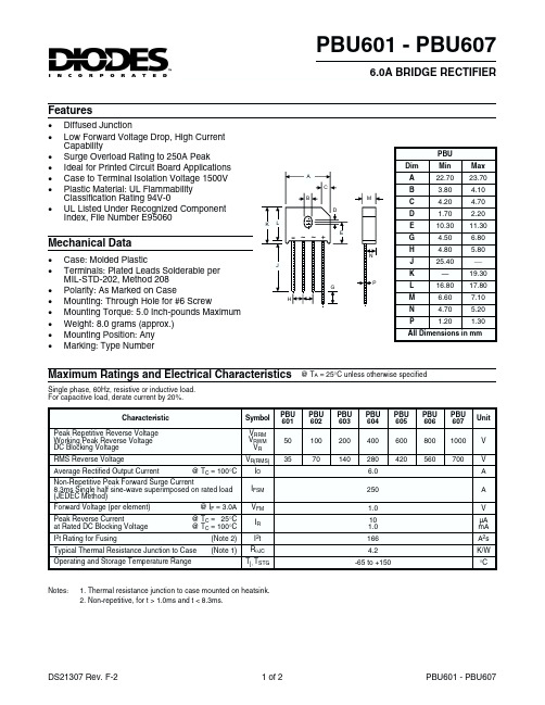
@ TC = 100°C
Non-Repetitive Peak Forward Surge Current 8.3ms Single half sine-wave superimposed on rated load (JEDEC Method)
Forward Voltage (per element)
· Polarity: As Marked on Case
· Mounting: Through Hole for #6 Screw
H
· Mounting Torque: 5.0 Inch-pounds Maximum
· Weight: 8.0 grams (approx.)
· Mounting Position: Any
DS21307 Rev. F-2
1 of 2
PBU601 - PBU607
元器件交易网
6 5
I(AV), AVERAGE OUTPUT CURRENT (A)
4 3
2
1 0 250
Single Phase Half Wave 60 Hz Resistive or Inductive Load
P
1.20
1.30
All DimensionБайду номын сангаас in mm
Maximum Ratings and Electrical Characteristics @ TA = 25°C unless otherwise specified
Single phase, 60Hz, resistive or inductive load. For capacitive load, derate current by 20%.
ICS601M-01ILF中文资料

ICS601-01 L OW P HASE N OISE C LOCK M ULTIPLIERDescriptionThe ICS601-01 is a low-cost, low phase noise,high-performance clock synthesizer for applications which require low phase noise and low jitter. It is ICS’ lowest phase noise multiplier, and also the lowest CMOS part in the industry. Using ICS’ patented analong and digital Phase-Locked Loop (PLL) techniques, the chip accepts a 10 - 27 MHz crystal or clock input, and produces output clocks up to 156 MHz at 3.3 V.This product is intended for clock generation. It has low output jitter (variation in the output period), but input and output skew and jitter are not defined nor guaranteed. For applications which require definted input to output timing, use the ICS670-01.Features•Packaged in 16-pin SOIC or TSSOP•Available in Pb (lead) free package•Uses fundamental 10 - 27 MHz crystal or clock •Patented PLL with the lowest phase noise •Output clocks up to 156 MHz at 3.3 V•Low phase noise: -132 dBc/Hz at 10 kHz•Low jitter - 18 ps one sigma typ.•Full swing CMOS outputs with 25 mA drive capability at TTL levels•Advanced, low power, sub-micron CMOS process •Industrial temperature range available •Operating voltage of 3.3V or 5VBlock DiagramPin AssignmentMultiplier Select Table0 = connect directly to ground 1 = connect directly to VDDPin DescriptionsS3S2S1S0CLK (see note 2 on following page)0000TEST 0001TEST 0010Input x10011Input x30100Input x40101Input x50110Input x60111Input x81000TEST1001Crystal osc. pass through (no PLL)1010Input x21011TEST 1100Input x81101Input x101110Input x121111Input x16Pin NumberPin Name Pin Type Pin Description1CLK Output Clock output from VCO. Output frequency equals the input frequency times multiplier.2REFEN Input Reference clock enable. Turns off the buffered crystal oscillator clock (stops low) when low.3VDD Power Connect to +3.3V or +5V . Must match other VDDs.4VDD Power Connect to +3.3V or +5V . Must match other VDDs.5VDD Power Connect to +3.3V or +5V . Must match other VDDs.6X2XO Crystal connection. Connect to a 10 - 27 MHz fundamental parallel mode crystal. Leave disconnected for an external clock input.7S1Input Multiplier select pin 1. Determines CLK output per table above. Internal pull-up.8X1/ICLK XI Crystal connection. Connect to a 10 - 27 MHz fundamental parallel mode crystal or clock.9S2Input Multiplier select pin 2. Determines CLK output per table above. Internal pull-up.10S3Input Multiplier select pin 3. Determines CLK output per table above. Internal pull-up.11S0Input Multiplier select pin 0. Determines CLK output per table above. Internal pull-up.12OE Input Output Enable. Tri-states both output clocks when low. Internal pull-up.13REFOUT Output Buffered crystal oscillator clock output. Controlled by REFIN.14 - 16GNDPowerConnect to ground.Achieving Low Phase NoiseFigure 1 shows a typical phase noise measurement in a 125 MHz system. Therea are a few simple steps that can be taken to achieve these levels of phase noise from the ICS601-01. Variations in VDD will increase the hase noise, so it is important to have a stable, low noise supply voltage at the device. Use decoupling capacitors of 0.1µF in parallel with 0.01µF . It is important to have these capacitors as close as possible to the ICS601-01 supply pins.Disabling the REFOUT clock is also important for achieving low phase noise; lab tests have shown that this can reduce the phase noise by as much as 10 dBc/Hz.External Component/Crystal SelectionThe ICS601-01 requires a minimum number of external components for proper operation. Decouplingcapacitors of 0.01µF and 0.1µF should be connected between VDD and GND, as close to the part as possible. A series termination resistor of 33Ω may be used for each clock output. The crystal must be connected as close to the chip as possible. The crystal should be fundamental mode, parallel resonant. Do not use third overtone. For exact tuning when using a crystal, capacitors should beconnected from pins X1 to ground and X2 to ground. In general, the value of these capacitors is given by the following equation, where CL is the crystal load capacitance: Crystal caps (pF) = (CL - 5) x 2. So for a crystal with 16 pF load capacitance, two 22 pF caps can be used. For any given board layout, ICS can measure the board capacitance and recommend the exact capacitance value to use.Absolute Maximum RatingsStresses above the ratings listed below can cause permanent damage to the ICS601-01. These ratings, which are standard values for ICS commercially rated parts, are stress ratings only. Functional operation of the device at these or any other conditions above those indicated in the operational sections of thespecifications is not implied. Exposure to absolute maximum rating conditions for extended periods can affect product reliability. Electrical parameters are guaranteed only over the recommended operating temperature range.Recommended Operation ConditionsDC Electrical CharacteristicsVDD=3.3 V ±10%, Ambient temperature -40 to +85°CItemRatingSupply Voltage, VDD 7 VAll Inputs and Outputs-0.5 V to VDD+0.5 V Ambient Operating Temperature, Commercial version 0 to +70 °C Ambient Operating Temperature, Industrial version -40 to +85 °C Storage Temperature -65 to +150 °C Junction Temperature 125 °C Soldering Temperature260 °CParameterMin.Typ.Max.UnitsAmbient Operating Temperature-40+85°C Power Supply Voltage (measured in respect to GND)+3.0+5.5VParameterSymbolConditionsMin.Typ.Max.UnitsOperating Voltage VDD 3.0 5.5V Input High Voltage V IH X1/ICLK pin only Note 1VDD/2+1VInput Low Voltage V IL X1/ICLK pin only Note 1VDD/2-1V Input High Voltage V IH 2V Input Low Voltage V IL 0.8V Output High VoltageV OHCMOS level I OH = -4mA VDD-0.4VI OH = -12mA 2.4Output Low VoltageV OLI OL = 12mA0.4VNote 1: Switching occurs nominally at VDD/2AC Electrical CharacteristicsVDD = 3.3V ±10%, Ambient Temperature -40 to +85° CNote 2: Input frequency limited by maximum output frequency and multiplication factor (I.e. For 16x, maximum input frequency is 13.75 MHz).Operating Supply Current IDD No load, 125 MHz 2230mA Short Circuit Current Each output ±40±60mA Input CapacitanceC INOE, select pins5pFParameterSymbolConditionsMin.Typ.Max.UnitsInput Frequency Fin1027MHz Output Frequency at 3.3V or 5V 156MHz Output Rise Time t OR 0.8 to 2.0V no load 1.5ns Output Fall Time t OF0.8 to 2.0V, no load 1.5ns Output Clock Duty Cycle at VDD/2455055%Maximum Absolute jitter, short term, 125 MHzNo load ±50±75ps Maximum jitter, one sigma, 125 MHz (x5)No load 1220ps Phase Noise, relative to carrier, 125 MHz (x5)100 Hz offset -90-94dBc/Hz Phase Noise, relative to carrier, 125 MHz (x5)1 kHz -116-120dBc/Hz Phase Noise, relative to carrier, 125 MHz (x5)10 kHz offset -118-122dBc/Hz Phase Noise, relative to carrier, 125 MHz (x5)100 kHz offset-115-119dBc/HzParameterSymbolConditionsMin.Typ.Max.UnitsPackage Outline and Package Dimensions (16 pin SOIC, 150 Mil. Narrow Body)Package dimensions are kept current with JEDEC Publication No. 95Package Outline and Package Dimensions (16-pin TSSOP,4.40 mm Body, 0.65 mm Pitch)Package dimensions are kept current with JEDEC Publication No. 95Ordering Information“L ” designates Pb (lead) free package; “I” designates industrial grade.While the information presented herein has been checked for both accuracy and reliability, Integrated Circuit Systems (ICS) assumes no responsibility for either its use or for the infringement of any patents or other rights of third parties, which would result from its use. No other circuits, patents, or licenses are implied. This product is intended for use in normal commercial applications. Any other applications such as those requiring extended temperature range, high reliability, or other extraordinary environmental requirements are not recommended withoutadditional processing by ICS. ICS reserves the right to change any circuitry or specifications without notice. ICS does not authorize or warrant any ICS product for use in life support devices or critical medical instruments.Part / Order NumberMarkingShipping PackagingPackageTemperatureICS601M-01ICS601M-01Tubes 16-pin narrow SOIC 0 to 70° C ICS601M-01T ICS601M-01Tape and Reel16-pin narrow SOIC 0 to 70° C ICS601M-01I ICS601M-01I Tubes 16-pin narrow SOIC -40 to 85° C ICS601M-01IT ICS601M-01I Tape and Reel16-pin narrow SOIC -40 to 85° C ICS601M-01LF ICS601M-01LF Tubes 16-pin narrow SOIC 0 to 70° C ICS601M-01LFT ICS601M-01LF Tape and Reel16-pin narrow SOIC 0 to 70° C ICS601M-01ILF ICS601M01ILF Tubes 16-pin narrow SOIC -40 to 85° C ICS601M-01ILFT ICS601M01ILF Tape and Reel16-pin narrow SOIC -40 to 85° C ICS601G-01601G-01Tubes 16-pin TSSOP 0 to 70° C ICS601G-01T 601G-01Tape and Reel16-pin TSSOP 0 to 70° C ICS601G-01I 601G-01I Tubes 16-pin TSSOP -40 to 85° C ICS601G-01IT 601G-01I Tape and Reel16-pin TSSOP -40 to 85° C ICS601G-01LF 601G01LF Tubes 16-pin TSSOP 0 to 70° C ICS601G-01LFT 601G01LF Tape and Reel16-pin TSSOP 0 to 70° C ICS601G-01ILF 601G01IL Tubes 16-pin TSSOP -40 to 85° C ICS601G-01ILFT601G01ILTape and Reel16-pin TSSOP-40 to 85° C。
一号柱电子技术有限公司GBU6005A至GBU610A型号的桥矩阵电源电路模块说明书
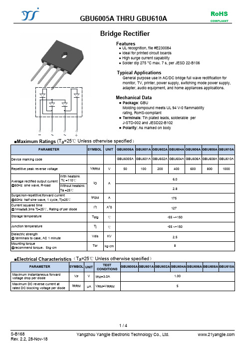
GBU6005A THRU GBU610ABridge RectifierFeatures● UL recognition, file #E230084 ● Ideal for printed circuit boards ● High surge current capability ● Solder dip 275 °C max. 7 s, per JESD 22-B106Typical ApplicationsGeneral purpose use in AC/DC bridge full wave rectification for monitor, TV, printer, power supply, switching mode power supply, adapter, audio equipment, and home appliances applications.Mechanical Data● P ackage : GBUMolding compound meets UL 94 V-0 flammability rating, RoHS-compliant● Terminals : Tin plated leads, solderable per J-STD-002 and JESD22-B102 ● Polarity: As marked on bodyCOMPLIANTRoHS~~■ Characteristics (Typical)`0.10.20.5FIG3: Forward Voltage1.010*******.0Instantaneous Forward Voltage (V )I n s t a n t a n e o u s F o r w a r d C u r r e n t (A )204060801000.010.11.010100FIG4:Typical Reverse CharacteristicsPercent of Rated Peak Reverse Voltage (%)I n s t a n t a n e o u s R e v e r s e C u r r e n t (u A )1025102050100100200300FIG2:Surge Forward Current CapabilityNumber of CyclesP e a k F o r w a r d S u r g e C u r r e n t (A )1FIG1:Io-Tc Curve23567Case Temperature (℃)A v e r a g e F o r w a r d O u t p u t (A )■Outline DimensionsDisclaimerThe information presented in this document is for reference only. Yangzhou Yangjie Electronic Technology Co., Ltd. reserves the right to make changes without notice for the specification of the products displayed herein to improve reliability, function or design or otherwise.The product listed herein is designed to be used with ordinary electronic equipment or devices, and not designed to be used with equipment or devices which require high level of reliability and the malfunction of with would directly endanger human life (such as medical instruments, transportation equipment, aerospace machinery, nuclear-reactor controllers, fuel controllers and other safety devices), Yangjie or anyone on its behalf, assumes no responsibility or liability for any damages resulting from such improper use of sale.This publication supersedes & replaces all information previously supplied. For additional information, please visit our website http:// , or consult your nearest Yangjie’s sales office for further assistance.。
中英文对照视音频术语汇编
术语汇编4:2:2 -分量数字视频格式的常用术语。
其格式细节由ITU-R BT.601 标准文件所规定。
数字4:2:2 表示信号的亮度通道与两个色差通道的抽样频率比。
每出现4 个亮度值,在两个色差通道中就各有两个色度样值。
见ITU-R BT.601。
4fsc -4 倍副载波抽样率,用于复合数字系统。
在NTSC 制中,该值为14.3MHz(4X3.58M),在PAL 制中为17.7MHz(4X4.43M)。
在标准清晰度中,525/60 和625/50 扫描格式的亮度分量样值均为13.5MHz,色度分量样值为6.75MHz。
AES/EBU 音频-由音频工程协会和欧洲广播联盟两个组织共同制定的数字音频标准。
它是非正式命名。
Algorithm -算法,以有限次处理解决问题的一套规则或过程。
Aliasing -混叠,由于数字视频中的抽样数太少或滤波不良而产生一种典型的图像缺陷。
这种缺陷一般表现为对角线上的锯齿状图形以及图像细节的闪烁或发亮。
Analog -模拟,用以描述连续变化的信号,它与数字信号相对应,后者包含的是用二进制数字0和1表示的离散电平。
Ancillary data -辅助数据,用以支持视频信号或视频节目的数据。
辅助数据是以时间复用的形式插入到视频信号的行消隐和(或)场消隐期间。
它可以在行消隐期内的EAV和SAV 数据包之间传送,也可以在场消隐期内以较大的数据包形式传送。
辅助数据可以包括校验和、多通道数字音频和其它数据。
Asynchronous -异步,一种不与时钟同步的传输过程。
数字视频是非异步的传输方式,因为抽样时钟信息可以从解码转换的数据信号中抽取。
A-to-D Converter (analog-to-digital) -模数转换器(模拟至数字),一种数字抽样电路,它可将模拟信号转换为该信号的数字表示。
Bandwidth -带宽,1)频率的上、下限之差,通常用兆赫(MHz)来度量。
2)一个完整的频率范围,在此范围内,电路或电子系统运行时的信号损耗小于3dB。
关于ITU BT 601与ITU BT656的一点基础知识

使用BT.656并行接口传输4路CIF格式视频的数据结构。
视频处理器的输出是灵活多变的,可以改变处理器的输出数据结构来同时传送4路252×288像素的视频信号。BT.656并行接口传输的有效视频数据流为720×586,正好可以分割为4个360×288像素的空间来传输4路352×288像素的视频数据。多余的空间用固定数据“8010”进行填充。
CCIR601号建议的制定,是向着数字电视广播系统参数统一化、标准化迈出 的第一步。在该建议中,规定了625和525行系统电视中心演播室数字编码的基 本参数值。601号建议单独规定了电视演播室的编码标准。它对彩色电视信号的编 码方式、取样频率、取样结构都作了明确的规定。规定彩色电视信号采用分量编码。所谓分量编码就是彩色全电视信号在转换成数字形式之前,先被分离成亮度信号和色差信号,然后对它们分别 进行编码。分量信号(Y、B -- Y、R -- Y)被分别编码后,再合成数字信号。
图5中,最高位bit7为固定数据1;F=0表示偶数场,F=1表示奇数场;V=0表示该行为有效视频数据,V=1表示该行没有有效视频数据;H=0表示为SAV信号,H=1表示为EAV信号;P3~P0为保护信号,由F、V、H信号计算生成;P3=V异或H;P2=F异或H;P1=F异或V;P0=F异或V异或H。
它规定了编码方式。对亮度信号和两个色差信同时,规定在数字编码时,不使用A/D转换的整个动态范围,只给亮度信号分配220个量化级,黑电平对应于量化级16,白电平对应于量化级235。为每个色差信号分配224个量化级,色差信号的零电平对应于量化级128。
BT.656每行的数据结构如图4所示。
图4中,每行数据包含水平控制信号和YCbCr。视频数据信号。视频数据信号排列顺序为Cb-Y-Cr-Y。每行开始的288字节为行控制信号,开始的4字节为EAV信号(有效视频结束),紧接着280个固定填充数据,最后是4字节的SAV信号(有效视频起始)。
GBU601中文资料
DS21226 Rev. D-2
1 of 2
GBU6005-GBU610
元器件交易网
IO, AVERAGE RECTIFIED CURRENT (A)
With heatsink
5 4
IF, INSTANTANEOUS FORWARD CURRENT (A)
6
100
10
Tj = 25°C
0.1 0.0 0.2 0.6 1.0 1.4 1.8 VF, INSTANTANEOUS FORWARD VOLTAGE (V) Fig. 2 Typical Forward Characteristics
IFSM, PEAK FORWARD SURGE CURRENT (A)
180 160
Single half-sine-wave (JEDEC method)
元器件交易网
GBU6005 - GBU610
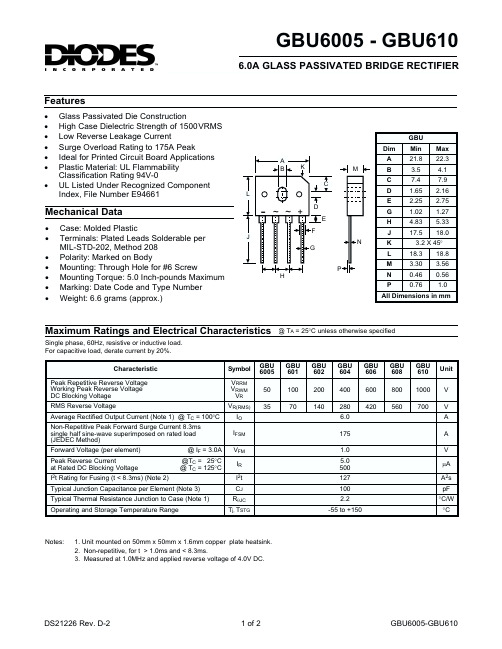
6.0A GLASS PASSIVATED BRIDGE RECTIFIER Features
· · · · · · · Glass Passivated Die Construction High Case Dielectric Strength of 1500VRMS Low Reverse Leakage Current Surge Overload Rating to 175A Peak Ideal for Printed Circuit Board Applications Plastic Material: UL Flammability Classification Rating 94V-0 UL Listed Under Recognized Component Index, File Number E94661
伯恩索马特电气焊接金属,银含量矿核无铅焊线说明书

SAFETY DATA SHEET1. IdentificationProduct identifierBernzOmatic Electrical Solder, Silver bearing rosin core lead-free solder Other means of identificationSDS number WC037Recommended use Soldering electrical connections Recommended restrictions None known.Manufacturer/Importer/Supplier/Distributor informationManufacturer/SupplierWorthington Cylinder Corporation Address 300 E. Breed St., Chilton, WI 53014United States Contact personKurt GoomeyE-mail address Telephone number 1-920-849-1740Emergency telephone number1-703-527-3887 International / CHEMTREC 1-800-424-9300 Domestic2. Hazard(s) identificationNot classified.Physical hazards Not classified.Health hazards Category 1Hazardous to the aquatic environment, acute hazard Environmental hazards Not classified.OSHA defined hazards Label elementsNone.Hazard symbol Signal word None.Hazard statement Very toxic to aquatic life.Precautionary statementPreventionAvoid release to the environment.Response Collect spillage.Storage Store away from incompatible materials.DisposalDispose of contents/container in accordance with local/regional/national/international regulations.Hazard(s) not otherwise classified (HNOC)None known.3. Composition/information on ingredientsMixtures7440-31-590 - 100Tin CAS number %Chemical name 7440-50-8 1 - 10Copper 65997-06-0< 1Rosin 7440-22-4< 1SilverComposition commentsAll concentrations are in percent by weight unless ingredient is a gas. Gas concentrations are in percent by volume.84711534. First-aid measuresInhalation Immediately remove from further exposure. Get immediate medical assistance. For thoseproviding assistance, avoid exposure to yourself or others. Use adequate respiratory protection.Give supplemental oxygen, if available. If breathing has stopped, assist ventilation with amechanical device or use mouth-to-mouth resuscitation.Skin contact Remove contaminated clothes and rinse skin thoroughly with water for at least 15 minutes. If skinrash or an allergic skin reaction develops, get medical attention.Eye contact Rinse immediately with plenty of water for at least 15 minutes. Remove any contact lenses. Getmedical attention if irritation develops or persists.Ingestion Immediately rinse mouth and drink a cupful of water. Never give anything by mouth to a victim whois unconscious or is having convulsions. Only induce vomiting at the instruction of medicalpersonnel. Get medical attention immediately.Most importantsymptoms/effects, acute and delayed Elevated temperatures or mechanical action may form dust and fumes which may be irritating to the eye, mucous membranes and respiratory tract. Symptoms may include stinging, tearing, redness, swelling, and blurred vision. Symptoms may include redness, edema, drying, defatting and cracking of the skin. Symptoms may include coughing, difficulty breathing and shortness of breath. Overexposure to copper fumes may cause fever, chills, congestion and headaches.Indication of immediate medical attention and special treatment needed Treat symptomatically. Exposure may aggravate pre-existing respiratory disorders. Symptoms may be delayed.General information Show this safety data sheet to the doctor in attendance.5. Fire-fighting measuresSuitable extinguishing media Extinguish with foam, carbon dioxide or dry powder. Unsuitable extinguishingmediaDo not use water or halogenated extinguishing media.Specific hazards arising fromthe chemicalFire or high temperatures create: Metal oxides.Special protective equipmentand precautions for firefightersUse protective equipment appropriate for surrounding materials.Fire-fighting equipment/instructions Self-contained breathing apparatus and full protective clothing must be worn in case of fire. Move containers from fire area if you can do it without risk.Specific methods Use standard firefighting procedures and consider the hazards of other involved materials. General fire hazards Solid metal is not flammable; however, finely divided metallic dust or powder may form anexplosive mixture with air.6. Accidental release measuresPersonal precautions, protective equipment and emergency procedures Keep unnecessary personnel away. Avoid inhalation of dust from the spilled material. Do not touch damaged containers or spilled material unless wearing appropriate protective clothing. Wear protective clothing as described in Section 8 of this SDS.Methods and materials for containment and cleaning up Stop leak if you can do so without risk. For a dry material spill, use a HEPA (high efficiency particle air) vacuum to collect material and place in a sealable container for disposal. Avoid dust formation. Recover and recycle, if practical. Keep out of water supply. Local authorities should be advised if significant spillages cannot be contained.Environmental precautions Prevent further leakage or spillage if safe to do so. Do not contaminate water.If release occurs in the U.S. and is reportable under CERCLA Section 103, notify the NationalResponse Center at (800)424-8802 (USA) or (202)426-2675 (USA).7. Handling and storagePrecautions for safe handling Wear appropriate personal protective equipment (See Section 8). Keep formation of airborne duststo a minimum. Provide appropriate exhaust ventilation at places where dust is formed. Avoidinhalation of dust and fumes. Avoid contact with skin and eyes. Do not get this material onclothing. Do not eat, drink or smoke when using the product. Wash thoroughly after handling.Avoid release to the environment.Any surface that comes in contact with molten metal must be preheated or specially coated andrust free. Inadvertent contaminants to product such as moisture, ice, snow, grease, or oil cancause an explosion when charged to a molten metal bath or metal furnace (preheating metal willremove moisture from product).Conditions for safe storage, including any incompatibilities Store in tightly closed original container in a dry, cool and well-ventilated place. Store in a closed container away from incompatible materials. Keep out of reach of children. Keep away from food, drink and animal feedingstuffs.8. Exposure controls/personal protectionOccupational exposure limitsUS. OSHA Table Z-1 Limits for Air Contaminants (29 CFR 1910.1000)Value Type Form ComponentsPEL 1 mg/m3Dust and mist.Copper (CAS 7440-50-8)0.1 mg/m3Fume.PEL 0.01 mg/m3Silver (CAS 7440-22-4)PEL2 mg/m3Tin (CAS 7440-31-5)US. ACGIH Threshold Limit Values Value Type FormComponentsTWA 1 mg/m3Dust and mist.Copper (CAS 7440-50-8)0.2 mg/m3Fume.TWA 0.1 mg/m3Dust and fume.Silver (CAS 7440-22-4)TWA2 mg/m3Tin (CAS 7440-31-5)US. NIOSH: Pocket Guide to Chemical Hazards Value Type Form ComponentsTWA 1 mg/m3Dust and mist.Copper (CAS 7440-50-8)TWA 0.01 mg/m3Dust.Silver (CAS 7440-22-4)TWA2 mg/m3Tin (CAS 7440-31-5)Biological limit values No biological exposure limits noted for the ingredient(s).Exposure guidelines No exposure standards allocated.Appropriate engineering controlsProvide adequate ventilation. Observe Occupational Exposure Limits and minimize the risk of inhalation of dust. Keep melting/soldering temperatures as low as possible to minimize the generation of fume. Shower, hand and eye washing facilities near the workplace are recommended.Individual protection measures, such as personal protective equipmentEye/face protectionWear safety glasses with side shields (or goggles). Wear a face shield when working with molten material.Skin protectionHand protectionWhen handling hot material, use heat resistant gloves.OtherChemical resistant clothing is recommended. Heat resistant/insulated gloves and clothing are recommended when working with molten material.Respiratory protectionUse a respirator when local exhaust or ventilation is not adequate to keep exposures below the OEL. In a confined space a supplied respirator may be required. Selection and use of respiratory protective equipment should be in accordance with OSHA General Industry Standard 29 CFR 1910.134; or in Canada with CSA Standard Z94.4. Use a NIOSH/MSHA approved respirator if there is a risk of exposure to dust/fume at levels exceeding the exposure limits.Thermal hazards Wear appropriate thermal protective clothing, when necessary.General hygiene considerationsAlways observe good personal hygiene measures, such as washing after handling the material and before eating, drinking, and/or smoking. Routinely wash work clothing and protective equipment to remove contaminants.9. Physical and chemical propertiesAppearanceSilver to silver-gray metallic metal.Physical state Solid.Form Solid.Color Silver to gray.OdorOdorless.Odor threshold Not available.pHNot applicable Melting point/freezing point Not available.Initial boiling point and boiling range 440.96 - 482 °F (227.2 - 250 °C)Flash pointNot available.Evaporation rate Not available.Flammability (solid, gas)Not available.Upper/lower flammability or explosive limitsFlammability limit - lower(%)Not available.Flammability limit - upper(%)Not available.Vapor pressure Not applicableVapor density Not available.Relative density7.38Solubility(ies)Solubility (water)Not solublePartition coefficient(n-octanol/water)Not available.Auto-ignition temperature Not available.Decomposition temperature Not available.Viscosity Not applicable10. Stability and reactivityReactivity The product is stable and non-reactive under normal conditions of use, storage and transport. Chemical stability Material is stable under normal conditions.Possibility of hazardousreactionsHazardous polymerization does not occur.Conditions to avoid Contact with incompatible materials. Avoid molten metal contact with water.Incompatible materials Chlorine. Turpentine. Magnesium. Acetylene Gas.Hazardous decompositionproductsToxic metal oxides are emitted when heated above the melting point.11. Toxicological informationInformation on likely routes of exposureIngestion Ingestion of dusts generated during working operations may cause nausea and vomiting. Copperpoisoning can result in hemolytic anemia and kidney, liver and spleen damage.Inhalation May cause respiratory tract irritation. Lung damage and possible pulmonary edema can resultfrom dust exposure. Inhalation of powder or fumes may cause metal fume fever.Skin contact May cause skin irritation. Hot or molten material may produce thermal burns.Eye contact Elevated temperatures or mechanical action may form dust and fumes which may be irritating tothe eyes.Symptoms related to the physical, chemical and toxicological characteristics Elevated temperatures or mechanical action may form dust and fumes which may be irritating to the eye, mucous membranes and respiratory tract. Contact with molten material may cause thermal burns. Symptoms may include stinging, tearing, redness, swelling, and blurred vision. Symptoms may include redness, edema, drying, defatting and cracking of the skin. Symptoms may include coughing, difficulty breathing and shortness of breath. Overexposure to copper fumes may cause fever, chills, congestion and headaches.Information on toxicological effectsAcute toxicity High concentrations of freshly formed fumes/dusts of metal oxides can produce symptoms ofmetal fume fever. When heated, the vapors/fumes given off may cause respiratory tract irritation.Overexposure of Tin can cause irritation of the eyes, skin, mucous membranes, and respiratorysystem. Acute overexposure to Copper dust/fume can cause irritation of the eyes, nose, throat,and skin and under severe fume overexposure can cause metal fume fever with flu-like symptomssuch as sweet metal taste, dry throat, coughing, fever and chills, tight chest, dyspnea, headache,blurred vision, back pain, nausea, vomiting, fatigue. Symptoms usually disappear within 24 hours.Copper may cause skin and hair discoloration. Inhalation of copper dusts may change the gumsand mucous lining of the mouth which is generally attributable to localized tissue effect rather thangeneral toxicity.Test ResultsComponentsSpecies Silver (CAS 7440-22-4)LD50Rat Oral Acute > 5000 mg/kgSkin corrosion/irritation Not classified.Serious eye damage/eye irritationElevated temperatures or mechanical action may form dust and fumes which may be irritating to the eye.Respiratory or skin sensitizationRespiratory sensitizationNot classified.Skin sensitization No sensitizing effects known.Germ cell mutagenicity Not classified.CarcinogenicityNot classifiable as to carcinogenicity to humans.OSHA Specifically Regulated Substances (29 CFR 1910.1001-1050)Not listed.Reproductive toxicityNot classified.Specific target organ toxicity -single exposureNot classified.Specific target organ toxicity -repeated exposure Not classified.Aspiration hazard Due to the physical form of the product it is not an aspiration hazard.Chronic effectsProlonged and repeated overexposure to dust and fumes can lead to benign pneumoconiosis (stannosis). Overexposure to Tin can result in benign pneumoconiosis (stannous). This form of pneumoconiosis produces progressive x-ray changes of the lungs as long as exposure exists, but there is no distinctive fibrosis, no evidence of disability and no special complicating factors.Ingestion of silver may cause a permanently benign bluish gray discoloration to the skin (argyria).12. Ecological informationEcotoxicityAlloys in massive forms present a limited hazard for the environment. Very toxic to aquatic life.ComponentsTest ResultsSpeciesCopper (CAS 7440-50-8)Aquatic EC50Crustacea 0.0076 - 0.026 mg/l, 48 hours Water flea (Daphnia obtusa)LC50Fish0.0051 - 0.015 mg/l, 96 hoursBony fish superclass (Osteichthyes)Silver (CAS 7440-22-4)Aquatic EC50Crustacea 0.0002 mg/l, 48 hoursWater flea (Daphnia magna)LC50Fish0.0019 - 0.003 mg/l, 96 hoursFathead minnow (Pimephales promelas)Persistence and degradability The product is not biodegradable.Bioaccumulative potential No data available.Mobility in soil Alloys in massive forms are not mobile in the environment.Other adverse effectsNone known.13. Disposal considerationsDisposal instructions Dispose in accordance with all applicable regulations.Local disposal regulations Dispose of in accordance with local regulations.Hazardous waste code Product contains silver a hazardous waste constituent regulated under 40 CFR 261.24.Waste from residues / unused productsDispose of in accordance with local regulations. Scrapped material should be sent for refining to recover precious metal content. Solid metal and alloys in the form of particles may be reactive. Its hazardous characteristics, including fire and explosion, should be determined prior to disposal.Contaminated packagingDispose of in accordance with local regulations.14. Transport informationDOTNot regulated as dangerous goods.IATANot regulated as dangerous goods.IMDGNot regulated as dangerous goods.Not applicable.Transport in bulk according toAnnex II of MARPOL 73/78 andthe IBC Code15. Regulatory informationUS federal regulations This product is a "Hazardous Chemical" as defined by the OSHA Hazard CommunicationStandard, 29 CFR 1910.1200.All components are on the U.S. EPA TSCA Inventory List.TSCA Section 12(b) Export Notification (40 CFR 707, Subpt. D)Not regulated.OSHA Specifically Regulated Substances (29 CFR 1910.1001-1050)Not listed.CERCLA Hazardous Substance List (40 CFR 302.4)Copper (CAS 7440-50-8)LISTEDSilver (CAS 7440-22-4)LISTEDSuperfund Amendments and Reauthorization Act of 1986 (SARA)Hazard categories Immediate Hazard - YesDelayed Hazard - NoFire Hazard - NoPressure Hazard - NoReactivity Hazard - NoSARA 302 Extremely hazardous substanceNot listed.YesSARA 311/312 HazardouschemicalSARA 313 (TRI reporting)Chemical name CAS number% by wt.Copper7440-50-8 1 - 10Other federal regulationsClean Air Act (CAA) Section 112 Hazardous Air Pollutants (HAPs) ListNot regulated.Clean Air Act (CAA) Section 112(r) Accidental Release Prevention (40 CFR 68.130)Not regulated.Not regulated.Safe Drinking Water Act(SDWA)US state regulationsUS. Massachusetts RTK - Substance ListCopper (CAS 7440-50-8)Silver (CAS 7440-22-4)Tin (CAS 7440-31-5)US. New Jersey Worker and Community Right-to-Know ActCopper (CAS 7440-50-8)Silver (CAS 7440-22-4)Tin (CAS 7440-31-5)US. Pennsylvania Worker and Community Right-to-Know LawCopper (CAS 7440-50-8)Silver (CAS 7440-22-4)Tin (CAS 7440-31-5)US. Rhode Island RTKCopper (CAS 7440-50-8)Silver (CAS 7440-22-4)US. California Proposition 65California Safe Drinking Water and Toxic Enforcement Act of 1986 (Proposition 65): This material is not known to contain any chemicals currently listed as carcinogens or reproductive toxins.US - California Proposition 65 - Carcinogens & Reproductive Toxicity (CRT): Listed substanceNot listed.International InventoriesCountry(s) or region Inventory nameOn inventory (yes/no)*Australian Inventory of Chemical Substances (AICS)YesAustralia Domestic Substances List (DSL)Yes Canada Non-Domestic Substances List (NDSL)No Canada Inventory of Existing Chemical Substances in China (IECSC)Yes China European Inventory of Existing Commercial Chemical Substances (EINECS)Yes Europe European List of Notified Chemical Substances (ELINCS)No Europe Inventory of Existing and New Chemical Substances (ENCS)No Japan Existing Chemicals List (ECL)Yes Korea New Zealand InventoryYes New Zealand Philippine Inventory of Chemicals and Chemical Substances (PICCS)Yes Philippines*A "Yes" indicates this product complies with the inventory requirements administered by the governing country(s).A "No" indicates that one or more components of the product are not listed or exempt from listing on the inventory administered by the governing country(s).Toxic Substances Control Act (TSCA) InventoryYesUnited States & Puerto Rico16. Other information, including date of preparation or last revisionIssue date 07-August-2014Revision date -Version #01HMIS® ratingsHealth: 1Flammability: 0Physical hazard: 0DisclaimerAll information in this Material Safety Data Sheet is believed to be accurate and reliable. However,no guarantee or warranty of any kind is made with regard to the accuracy of information or the suitability of the recommendations contained herein. It is the user’s responsibility to assess the safety and toxicity of this product under their own conditions of use and to comply with all applicable laws and regulations.。
GBU608中文资料

100
Tj = 25°C f = 1.0MHz
120
Cj, JUNCTION CAPACITANCE (pF)
100
Tj = 25°C
80
10
40
0
1
10
1 1 10 VR, REVERSE VOLTAGE (V) Fig. 4 Typical Junction Capacitance 100
NUMBER OF CYCLES AT 60 Hz Fig. 3 Maximum Non-Repetitive Surge Current
3
Without heatsink
2 1
Resistive or Inductive load
1.0
Pulse width = 300µs
0 0 25 50 75 100 125 150 TC, CASE TEMPERATURE (°C) Fig. 1 Forward Current Derating Curve
DS21226 Rev. D-2
2 of 2
GBU6005-GBU610
GBU Dim
A B K C L
Min 21.8 3.5 7.4 1.65 2.25 1.02 4.83 17.5 18.3 3.30 0.46 0.76
Max 22.3 4.1 7.9 2.16 2.75 1.27 5.33 18.0 18.8 3.56 0.56 1.0
A
M
B C D E G H J
J
-
~ ~ +
D E F G P N
K L M N P
3.2 X 45°
H
All Dimensions in mm
Maximum Ratings and Electrical Characteristics
abs hu601技术参数

ABS HU601技术参数ABS HU601 是一种用于汽车防抱死制动系统 ABS)的芯片,具有较高的技术性能和可靠性。
以下是该芯片的一些主要技术参数:1. 工作电压:ABS HU601 芯片的工作电压通常在 12V 至 16V 之间,具体取决于汽车电源系统的电压。
2. 输入信号:该芯片需要接收来自轮速传感器、踏板位置传感器、ABS 控制器等设备的输入信号,以实现对制动系统的实时监测和控制。
3. 输出控制:ABS HU601 芯片具备多个输出控制接口,可以控制制动缸、制动泵、电子控制单元等设备的工作状态,实现对制动系统的精确控制。
4. 控制算法:该芯片采用先进的控制算法,能够快速、准确地检测到车轮的滑动状态,并根据实际情况进行相应的控制操作,以保证车辆在制动过程中的稳定性和安全性。
5. 通信接口:ABS HU601 芯片通常具备多种通信接口,如 CAN 总线、LIN 总线、SPI 接口等,可以方便地与其他汽车电子设备进行通信和数据交换。
6. 工作温度:ABS HU601 芯片的工作温度范围通常在 -40℃ 至 125℃ 之间,能够适应各种恶劣的工作环境。
7. 尺寸和封装:该芯片采用紧凑的尺寸和封装形式,可以方便地安装在汽车制动系统的电子控制模块中。
在选择和使用 ABS HU601 芯片时,需要根据汽车的具体型号和配置进行综合考虑,以确保芯片与汽车系统的兼容性和匹配性。
同时,还需要关注芯片的工作电压、输入输出信号、通信接口、工作温度等参数,以确保芯片的正常工作和稳定性能。
总之,ABS HU601 芯片是一种高性能的汽车防抱死制动系统芯片,具有较高的技术参数和可靠性,可以为汽车的安全性能提供有力保障。
在选择和使用这类芯片时,需要综合考虑各种因素,以确保芯片与汽车系统的兼容性和匹配性。
CP601中文资料
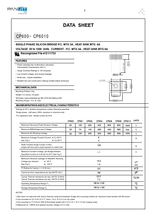
元器件交易网
INSTANTANEOUS FORWARD CURRENT, AMPERES
5.0 4.0 3.0 2.0 1.0 .9 .8 .7 .5 .3 .2 .1 .07 .05 .03 .02 .01 0 0.2 0.4 0.6 0.8 1.0 1.2 1.4
RATING AND CHARACTERISTIC CURVES
A2S pF °C/W °C °C
1.Bolt down on heat-sink with silicon thermal compound between bridge and mounting surface for maximum heat transfer with #6 screw. 2.Unit mounted on 5.0 X 6.0 X 0.11” thick ( 14 X 15 X 0.3 cm )AL.plate. 3.Unit mounted on P.C.B at 0.395”(9.5mm)lead length with 0.5 X 0.5” ( 12 X 12 mm )copper pads. 4.Measured at 1.0MHZ and applied reverse voltage of 4.0 volts.
FEATURES
• Plastic package has Underwriters Laboratory Flammability Classification 94V-O . • Surge Overload Ratings to 125 Amperes. • Low forward voltage, and reverse leakage. • Small size , simple installation. • Reliable low cost construction utilizing molded plastic technique.
诺雅克快速选型20130321

3P:三极 4P:四极
D/O:抽屉式 (可省略) F:固定式 W:仅抽架
B:仅本体
AC230: 交流230V AC400: 交流400V
DC220: 直流220V DC110: 直流110V DC24: 直流24V
仅抽架无 此代号
无特殊要求 此处无代号
可选附件的 代码可标注 于此
标配附件:
分励脱扣器、闭合电磁铁、闭合电磁铁、辅助触头
2000-2500-29003200-4000
1000
12
Q/R/H
Q/R/H
65/85/100 50/65/75
100%
50/65/85 35/40/50 143/187/220
100%
65/85/100 50/65/75
100%
50/65/85 35/40/50 143/187/220
105/143/165
N:55kA Q:65kA R:85kA H:100kA
9A16可选N、Q 9A32可选Q、R、H 9A40可选Q、R、H
3P:三极 4P:四极
16: 1600A,1250A, 1000A,800A, 630A,400A
32: 3200A,2900A, 2500A,2000A, 1600A
40: 4000A,3200A, 2900A,2500A, 2000A
12500 25000 6000 3000
固定式 254/324
323 213 22 26.5
抽屉式 282/352
352 303 38 55
■ 标准配置
□ 可选
—无
3200
4000
3P/4P
3P/4P
50/60
50/60
手机射频电路原理

双工滤波器(U601)
器件引脚排列及名称:
表1:器件引脚排列及名称
双工滤波器(U601)
表2:双工滤波器的开关控制模式
双工滤波器(U601)
图3:双工滤波器相关电路
声表面滤波器
3、声表面滤波器(Z600、Z602、Z603): 是一个带通滤波器,只允许接收频段的射频信号进入接收
机电路,其它频段的信号将会得到抑制。
射频收发信机(U602)
MT6129系列采用非常低中频结构(与零中频相比,能够改 善阻塞抑制、AM抑制、邻道选择性,不需DC偏移校正,对 SAW FILTER共模平衡的要求降低),采用镜像抑制 (35dB抑制比)混频滤波下变频到IF,第1中频频率为: GSM 200KHZ,DCS/PCS 100KHZ。第1IF信号通过镜像抑 制滤波器和PGA(每步2dB共78dB动态范围)进行滤波放大, 经第2混频器下变频到基带IQ信号,频率为67.708KHz。
手机通用的接收与发射流程
2、信号发射流程: 话音采集——放大——ADC——滤波——语音编
码——交织——加密——信道均衡——GMSK调制—— (进入射频部分)IQ调制(IQ调制器)——滤波—— 鉴相鉴频(鉴相鉴频器)——滤波——TX_VCO混频 (混频器Mixer)——功率放大(PA)——双工器—— 天线匹配电路——天线发射。
表3:引脚排列及名称
图4:内部结构
声表面滤波器
频率传输特性
声表面滤波器
射频收发信机(U602)
射频收发信机是射频电路的核心部件,主要完成射频信号 的调整与解调。内部结构主要包括5个方面:
1)、接收机(Receiver):提供射频信号的下行链路,将 射频信号通过放大、解调转变成IQ信号供基带芯片进行处 理。
601A使用说明书

eDCAP-601A通用保护测控装置使用说明书北京紫光测控有限公司BEIJING UNISPLENDOUR M&C CO. , LTD目录1 概述 (3)2装置主要功能配置 (3)3装置硬件资源配置 (4)4主要技术指标 (4)4.1 额定参数 (4)4.2 环境条件 (4)4.3 功率消耗 (5)4.4 热稳定性 (5)4.5 测控技术指标 (5)4.6 保护技术指标 (6)4.7 触点容量 (9)4.8 绝缘性能 (9)4.9 抗干扰能力 (9)5装置原理 (10)5.1 装置的构成 (10)5.2 保护原理说明 (10)6菜单及数据表格说明 (21)6.1 实时数据表 (22)6.2保护参数表 (24)6.3 通信数据表格 (29)6.4系统参数表 (33)6.5模拟量校准表 (33)7操作方法 (35)8装置结构及尺寸 (35)9装置原理接线图 (37)10箱后端子接线图 (38)1概述eDCAP-601A通用保护测控装置适用于110kV以下电压等级的不接地、经小电阻接地或经消弧线圈接地系统中的线路(进线或馈出线)、部分馈出设备(馈出变或接地变等)的保护及测控。
2 装置主要功能配置名称说明保护三段定时限过流保护(可受方向和复压判据控制);过流后加速保护(可受复压判据控制);过负荷保护;过负荷告警;充电保护;反时限过流保护;两段低压保护;过压保护;低周减载;三相多次重合闸,偷跳重合(即不对应重合);零序过压告警;三段零序过流保护(可受零序电压闭锁);零序后加速;零序过流告警;两段低压侧零序过流保护;独立的接地选线功能;PT断线、CT断线、控制回路断线、装置失电告警;合闸可检同期、检线路无压、检母线无压或不检;5路非电量保护(重瓦斯、轻瓦斯、高温跳闸、高温告警、压力释放);4路非电量控制(联跳1、2、3、4);故障、告警、闭锁、重合闸等事件记录;支持硬压板投退并可灵活整定;2套保护定值及保护投退;故障录波。
UT601电容表说明书
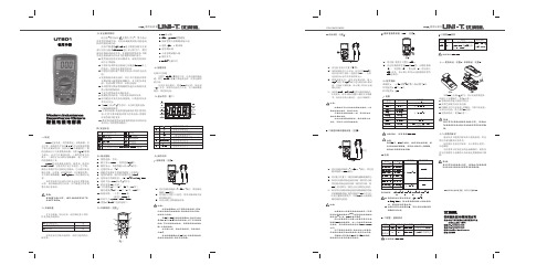
警告:在使用仪表之前,请仔细阅读有关 安全操作准则 。
一.概述UT601电容表是一种性能稳定、结构新颖、安全可靠、高精度的手持式3 1/2位手动切换量程数字非电压测试仪表。
仪表具有20个测量档位。
整机电路设计以大规模集成电路,双积分A/D转换器为核心,还可用于测量电阻、三极管的放大倍数β、二极管正向压降及电路通断。
是广大用户的理想维修工具。
UT601的电容测量范围宽、精度高,精度从0.1pF到20mF。
它能应用于电子实验室、生产线、维修点和教学等方面的电容测试;它还能用来检测公差值、分类值、选择精度值;并可测量电缆、开关和印刷线路板(PCB-LAYOUT)的电路设计电容。
本使用说明书包括有关的安全信息和警告提示等,请仔细阅读有关内容,并严格遵守所有的警告和注意事项。
二.开箱检查打开包装箱,取出仪表,请仔细检查下列附件是否缺少或损坏:如发现有任何缺少或损坏,请即与您的供应商联系。
三.安全操作准则请注意 警告标识 及警告字句 。
警告表示对使用者构成危险、对仪表或被测设备可能造成损坏的情况或行动。
仪表严格遵循GB4793.1电子测量仪器安全要求以及安全标准IEC61010进行设计和生产,使用前请仔细阅读此说明书,并遵循其使用说明,否则可能会削弱或失去仪表为您提供的保护能力。
1.使用前应检查仪表及测试夹,谨防任何损坏 或不正常现象。
2.不要在仪表终端及接地之间施加30Vrms以上 的电压,以防电击和损坏仪表。
3.后盖没有盖好前严禁使用仪表,否则有电击危 险。
4.更换保险丝或电池时,在打开后盖前应将带 夹测试线与被测量电路断开,并关闭仪表电 源。
仪表长期不用时,应取出电池。
5.必须使用同类标称规格的快速反应保险丝更 换已损坏的保险丝。
6.不允许使用该表去测试电压。
7.被测电容应放电,以防电击和损坏仪表。
8.请勿随意改变仪表内部接线,以免损坏仪表 和危及安全。
9.当LCD上显示 符号时,应及时更换电池, 以确保测量精度。
PbPbO和PbO
名称:铅;Lead元素符号pb,原子序数82,原子量207.2,外围电子排布6s26p2,位于第六周期ⅣA族,原子半径146皮米,Pb4+半径84皮米,第一电离能718.96kJ/mol,电负性1.8,主要氧化数+2、+4。
银灰色有光泽的重金属,在空气中易氧化而失去光泽,变灰暗,质柔软,延性弱,展性强。
密度11.34g/cm3,熔点327.5℃,沸点1740℃。
有较强的抗放射性穿透的性能。
有毒。
在常温下在空气中,铅表面易生成一层氧化铅或碱式碳酸铅,使铅失去光泽且防止进一步氧化。
不溶于水。
易和卤素、硫化合,生成PbCl4、PbI2、PbS等。
熔融的铅跟空气反应生成一氧化铅,将铅在纯氧中加热可得二氧化铅。
与盐酸反应放出氢气并生成微溶性的PbCl2,覆盖在铅表面,使反应中止。
与热浓盐酸反应生成HPbCl3和H2。
与稀硫酸反应放出氢并生成难溶的PbSO4覆盖层,使反应中止。
但易溶于热的浓硫酸生成Pb(HSO4)2并放出SO2。
跟稀硝酸或浓硝酸反应都可生成硝酸铅pb(NO3)2。
在有氧存在的条件下可溶于醋酸等有机酸,生成可溶性的铅盐。
跟强碱溶液缓慢的反应放出氢气生成亚铅酸盐,如:Pb+2NaOH=Na2PbO3+H2↑在有氧气条件下跟水反应生成难溶的Pb(OH)2。
铅早在公元前三千年左右就被人类发现并应用。
在地壳中质量百分比为0.0016%。
主要存在于方铅矿(PbS),白铅矿(PbCO3)中。
用作电缆,蓄电池、铸字合金、巴氏合金、金属结构的阴极保护层、防X射线等辐射的材料。
用焦炭还原氧化铅制得。
名称:一氧化铅;氧化铅;黄铅丹;密陀僧;Lead monoxidePbO 分子量223.19性状浅黄色或土黄色四角或斜方晶系结品体,或者无定形粉末。
四角晶系结晶体密度9.53g/cm3,斜方晶系结晶体密度3.0g/cm3,无定形粉末密度9.2~9.5g/cm3。
熔点888℃。
沸点1470℃。
不溶于水和乙醇,溶于硝酸、醋酸或温热的碱液。
- 1、下载文档前请自行甄别文档内容的完整性,平台不提供额外的编辑、内容补充、找答案等附加服务。
- 2、"仅部分预览"的文档,不可在线预览部分如存在完整性等问题,可反馈申请退款(可完整预览的文档不适用该条件!)。
- 3、如文档侵犯您的权益,请联系客服反馈,我们会尽快为您处理(人工客服工作时间:9:00-18:30)。
PBU601 - PBU607
6.0A BRIDGE RECTIFIER
Features
-
~~+
B
C
D
H
M
N
P
A
E
L
K
J
G
PBU
Dim
Min Max A 22.7023.70B 3.80 4.10C 4.20 4.70D 1.70 2.20E
10.3011.30G
4.50 6.80H 4.80
5.80J 25.40¾K —19.30L 1
6.801
7.80M 6.607.10N 4.70 5.20P
1.20
1.30
All Dimensions in mm
Maximum Ratings and Electrical Characteristics
@ T A = 25°C unless otherwise specified
Mechanical Data
Single phase, 60Hz, resistive or inductive load.For capacitive load, derate current by 20%.
Characteristic
Symbol PBU 601PBU 602PBU 603PBU 604PBU 605PBU 606PBU 607Unit Peak Repetitive Reverse Voltage Working Peak Reverse Voltage DC Blocking Voltage V RRM V RWM V R 50100
2004006008001000V RMS Reverse Voltage
V R(RMS)
35
70
140
280420
560
700
V Average Rectified Output Current
@ T C = 100°C
I O 6.0A Non-Repetitive Peak Forward Surge Current
8.3ms Single half sine-wave superimposed on rated load (JEDEC Method)
I FSM 250A Forward Voltage (per element)@ I F = 3.0A V FM 1.0V Peak Reverse Current
@ T C = 25°C at Rated DC Blocking Voltage @ T C = 100°C
I R 101.0µA mA I 2t Rating for Fusing
(Note 2)I 2t 166A 2s Typical Thermal Resistance Junction to Case (Note 1)
R q JC 4.2K/W Operating and Storage Temperature Range
T j,T STG
-65 to +150
°C
Notes:
1. Thermal resistance junction to case mounted on heatsink.
2. Non-repetitive, for t > 1.0ms and t < 8.3ms.
·Diffused Junction
·Low Forward Voltage Drop, High Current Capability
·Surge Overload Rating to 250A Peak
·Ideal for Printed Circuit Board Applications ·Case to Terminal Isolation Voltage 1500V ·Plastic Material: UL Flammability Classification Rating 94V-0
·
UL Listed Under Recognized Component Index, File Number E95060
·Case: Molded Plastic
·Terminals: Plated Leads Solderable per MIL-STD-202, Method 208·Polarity: As Marked on Case
·Mounting: Through Hole for #6 Screw
·Mounting Torque: 5.0 Inch-pounds Maximum ·Weight: 8.0 grams (approx.)·Mounting Position: Any ·
Marking: Type Number
0.11.0
10
I ,I N S T A N T A N E O U S F W D C U R R E N T (A )
F V ,INSTANTANEOUS FWD VOLTAGE (V)Fig.2Typical Forward Characteristics
F
100
0.6
0.70.80.9 1.0 1.1 1.2
1.30
50
100
150
200
2501
10100
I ,P E A K F W D S U R G E C U R R E N T (A )
F S M NUMBER OF CYCLES AT 60Hz
Fig.3Max Non-Repetitive Peak Fwd Surge Current
10
100
400
1
10100
C ,C A P A C I T A N C E (p F )
j V ,
REVERSE VOLTAGE (V)
Fig.4Typical Junction Capacitance Per Element
R 0.01
0.1
1.0
10
I ,I N S T A N T A N E O U S R E V E R S E C U R R E N T (m A )
R RATED PERCENT OF PEAK REVERSE VOLTAGE (%)
Fig.5Typical Reverse Characteristics
1
2345
20
406080100120140I ,A V E R A G E O U T P U T C U R R E N T (A )
(A V )T ,CASE TEMPERATURE (ºC)Fig.1Forward Current Derating Curve
C 6。
