74AVCH20T245ZQLR中文资料
74VCXH245DT资料
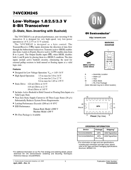
74VCXH245Low−Voltage 1.8/2.5/3.3 V 8−Bit Transceiver(3−State, Non−Inverting with Bushold)The 74VCXH245 is an advanced performance, non−inverting 8−bit transceiver. It is designed for very high−speed, very low−power operation in 1.8 V , 2.5 V or 3.3 V systems.The 74VCXH245 is designed as a byte control. The Transmit/Receive (T/Rn) inputs determine the direction of data flow through the bidirectional transceiver. Transmit (active−HIGH) enables data from A ports to B ports; Receive (active−LOW) enables data from B to A ports. The Output Enable input (OE), when HIGH, disables both A and B ports by placing them in a HIGH Z condition. The data inputs include active bushold circuitry, eliminating the need for external pullup resistors to hold unused or floating inputs at a valid logic state.Features•Designed for Low V oltage Operation: V CC = 1.65−3.6 V •High Speed Operation: 3.5 ns max for 3.0 to 3.6 V 4.2 ns max for 2.3 to 2.7 V 8.4 ns max for 1.65 to 1.95 V•Static Drive:±24 mA Drive at 3.0 V±18 mA Drive at 2.3 V ±6 mA Drive at 1.65 V•Includes Active Bushold to Hold Unused or Floating Data Inputs at a Valid Logic State•Near Zero Static Supply Current in All Three Logic States (20 m A)Substantially Reduces System Power Requirements •Latchup Performance Exceeds ±200 mA @ 85°C •ESD Performance:Human Body Model >2000 VMachine Model >200 V•Pb−Free Package is Available*For additional information on our Pb−Free strategy and soldering details, please download the ON Semiconductor Soldering and Mounting Techniques Reference Manual, SOLDERRM/D.MARKING DIAGRAMQFNMNR2 SUFFIX CASE 485AAA = Assembly Location L = Wafer Lot Y = Year W = Work Week G = Pb−Free Package(Note: Microdot may be in either location)Device Package Shipping †ORDERING INFORMATION74VCXH245MNR2QFN3000/T ape&Reel74VCXH245MNR2GQFN (Pb−Free)3000/T ape&Reel 1VCX H245ALYW G G†For information on tape and reel specifications,including part orientation and tape sizes, please refer to our T ape and Reel Packaging Specifications Brochure, BRD8011/D.Pinout (Top View)PIN #1291912201011QFNB0OE 19T/R 1A0B1A1B2A2B3A3B4A4B5A5B6A6B7A7Figure 1. Logic DiagramV CC = Pin 20GND = Pin 10H = High Voltage Level L = Low Voltage Level Z = High Impedance StateX = High or Low Voltage Level and Transitions are AcceptableABSOLUTE MAXIMUM RATINGSvalues (not normal operating conditions) and are not valid simultaneously. If these limits are exceeded, device functional operation is not implied,damage may occur and reliability may be affected.1.I O absolute maximum rating must be observed.RECOMMENDED OPERATING CONDITIONS (Note 2)Figure 2. 20 Pad QFN Suggested Board Layout (Bottom View)DC ELECTRICAL CHARACTERISTICSI4.An external driver must source at least the specified current to switch from LOW−to−HIGH.5.An external driver must sink at least the specified current to switch from HIGH−to−LOW.6.Outputs disabled or 3−state only.AC CHARACTERISTICS (Note 7; t = t = 2.0 ns; C = 30 pF; R = 500 W)L8.Skew is defined as the absolute value of the difference between the actual propagation delay for any two separate outputs of the same device.The specification applies to any outputs switching in the same direction, either HIGH−to−LOW (t OSHL) or LOW−to−HIGH (t OSLH); parameter guaranteed by design.DYNAMIC SWITCHING CHARACTERISTICSmeasured in the LOW state.10.Number of outputs defined as “n”. Measured with “n−1” outputs switching from HIGH−to−LOW or LOW−to−HIGH. The remaining output ismeasured in the HIGH state.CAPACITIVE CHARACTERISTICSCC I CCWAVEFORM 1 − PROPAGATION DELAYS t R = t F = 2.0 ns, 10% to 90%; f = 1 MHz; t W = 500 nsV IH0 V V OHV OL An, BnBn, AnWAVEFORM 2 − OUTPUT ENABLE AND DISABLE TIMES t R = t F = 2.0 ns, 10% to 90%; f = 1 MHz; t W = 500 nsV IH0 V ≈ 0VOEn, T/RnAn, Bn≈ V CC An, BnFigure 3. AC WaveformsV OH Vy Vx V OLOPENV 6 V or V CC × 2GNDC L = 30 pF or equivalent (Includes jig and probe capacitance)R L = 500 W or equivalentR T = Z OUT of pulse generator (typically 50 W )Figure 4. Test CircuitPACKAGE DIMENSIONSQFNMNR2 SUFFIX CASE 485AA−01ISSUE ADIMMIN MAX MILLIMETERS A A10.000.05A20.650.75A3b 0.200.30D 2.50 BSC D20.85 1.15E 4.50 BSC E2e 0.50 BSC K 0.20−−−NOTES:1.DIMENSIONING AND TOLERANCING PER ASME Y14.5M, 1994.2.CONTROLLING DIMENSION: MILLIMETERS.3.DIMENSIONS b APPLIES TO PLATEDTERMINAL AND IS MEASURED BETWEEN 0.25 AND 0.30 MM FROM TERMINAL.4.COPLANARITY APPLIES TO THE EXPOSED PAD AS WELL AS THE TERMINALS.0.20 REF 0.80 1.00L0.350.452.853.15ON Semiconductor and are registered trademarks of Semiconductor Components Industries, LLC (SCILLC). SCILLC reserves the right to make changes without further notice to any products herein. SCILLC makes no warranty, representation or guarantee regarding the suitability of its products for any particular purpose, nor does SCILLC assume any liability arising out of the application or use of any product or circuit, and specifically disclaims any and all liability, including without limitation special, consequential or incidental damages.“Typical” parameters which may be provided in SCILLC data sheets and/or specifications can and do vary in different applications and actual performance may vary over time. All operating parameters, including “Typicals” must be validated for each customer application by customer’s technical experts. SCILLC does not convey any license under its patent rights nor the rights of others. SCILLC products are not designed, intended, or authorized for use as components in systems intended for surgical implant into the body, or other applications intended to support or sustain life, or for any other application in which the failure of the SCILLC product could create a situation where personal injury or death may occur. Should Buyer purchase or use SCILLC products for any such unintended or unauthorized application, Buyer shall indemnify and hold SCILLC and its officers, employees, subsidiaries, affiliates, and distributors harmless against all claims, costs, damages, and expenses, and reasonable attorney fees arising out of, directly or indirectly, any claim of personal injury or death associated with such unintended or unauthorized use, even if such claim alleges that SCILLC was negligent regarding the design or manufacture of the part. SCILLC is an Equal Opportunity/Affirmative Action Employer. This literature is subject to all applicable copyright laws and is not for resale in any manner.PUBLICATION ORDERING INFORMATION。
74VHC245NX中文资料
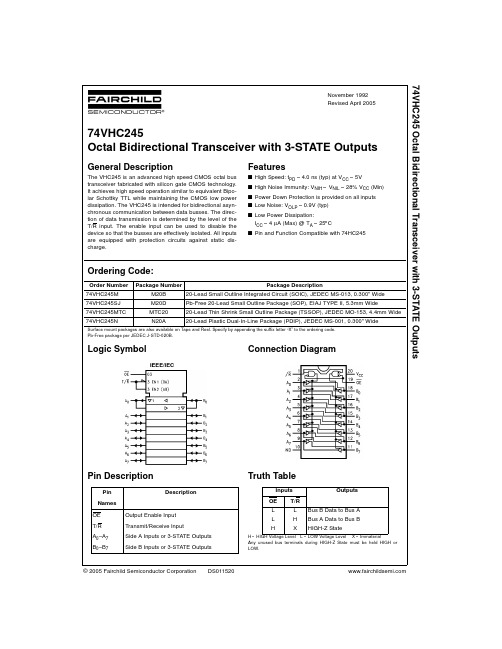
© 2005 Fairchild Semiconductor Corporation DS011520November 1992Revised April 200574VHC245 Octal Bidirectional Transceiver with 3-STATE Outputs74VHC245Octal Bidirectional Transceiver with 3-STATE OutputsGeneral DescriptionThe VHC245 is an advanced high speed CMOS octal bus transceiver fabricated with silicon gate CMOS technology.It achieves high speed operation similar to equivalent Bipo-lar Schottky TTL while maintaining the CMOS low power dissipation. The VHC245 is intended for bidirectional asyn-chronous communication between data busses. The direc-tion of data transmission is determined by the level of the T/R input. The enable input can be used to disable the device so that the busses are effectively isolated. All inputs are equipped with protection circuits against static dis-charge.Featuress High Speed: t PD 4.0 ns (typ) at V CC 5V s High Noise Immunity: V NIH V NIL 28% V CC (Min)s Power Down Protection is provided on all inputs s Low Noise: V OLP 0.9V (typ)s Low Power Dissipation:I CC 4 P A (Max) @ T A 25q Cs Pin and Function Compatible with 74HC245Ordering Code:Surface mount packages are also available on T ape and Reel. Specify by appending the suffix letter “X” to the ordering code.Pb-Free package per JEDEC J-STD-020B.Logic SymbolIEEE/IECPin DescriptionConnection DiagramTruth TableH HIGH Voltage Level L LOW Voltage Level X ImmaterialAny unused bus terminals during HIGH-Z State must be held HIGH or LOW.Order Number Package NumberPackage Description74VHC245M M20B 20-Lead Small Outline Integrated Circuit (SOIC), JEDEC MS-013, 0.300" Wide 74VHC245SJ M20D Pb-Free 20-Lead Small Outline Package (SOP), EIAJ TYPE II, 5.3mm Wide74VHC245MTC MTC2020-Lead Thin Shrink Small Outline Package (TSSOP), JEDEC MO-153, 4.4mm Wide 74VHC245NN20A20-Lead Plastic Dual-In-Line Package (PDIP), JEDEC MS-001, 0.300" WidePin DescriptionNames OE Output Enable Input T/R Transmit/Receive InputA 0–A 7Side A Inputs or 3-STATE OutputsB 0–B 7Side B Inputs or 3-STATE OutputsInputs OutputsOE T/R L L Bus B Data to Bus A L H Bus A Data to Bus B HXHIGH-Z State 274V H C 245Absolute Maximum Ratings (Note 1)Recommended Operating Conditions (Note 2)Note 1: Absolute Maximum Ratings are values beyond which the device may be damaged or have its useful life impaired. The databook specifica-tions should be met, without exception, to ensure that the system design is reliable over its power supply, temperature, and output/input loading vari-ables. Fairchild does not recommend operation outside databook specifica-tions.Note 2: Unused inputs or I/O pins must be held HIGH or LOW. They may not float.DC Electrical CharacteristicsSupply Voltage (V CC )0.5V to 7.0V DC Input Voltage (V IN ) (T/R, OE) 0.5V to 7.0V DC Output Voltage (V OUT ) 0.5V to V CC 0.5VInput Diode Current (I IK ) (T/R, OE) 20 mA Output Diode Current (I OK )r 20 mA DC Output Current (I OUT )r 25 mA DC V CC /GND Current (I CC )r 75 mAStorage Temperature (T STG ) 65q C to 150q CLead Temperature (T L )(Soldering, 10 seconds)260q CSupply Voltage (V CC ) 2.0V to 5.5V Input Voltage (V IN )(T/R, OE)0V to5.5V Output Voltage (V OUT )0V to V CCOperating Temperature (T OPR ) 40q C to 85q CInput Rise and Fall Time (t r , t f )V CC 3.3V r 0.3V 0 a 100 ns/V V CC 5.0V r 0.5V0 a 20 ns/V Symbol ParameterV CC T A 25q C T A 40q C to 85q C Units Conditions(V)Min TypMaxMin MaxV IH HIGH Level 2.0 1.50 1.50V Input Voltage 3.0 5.50.7 V CC0.7 V CCV IL LOW Level 2.00.500.50VInput Voltage 3.0 5.50.3 V CC0.3 V CC V OHHIGH Level 2.0 1.9 2.0 1.9V IN V IH I OH 50 P AOutput Voltage3.0 2.9 3.0 2.9Vor V IL4.5 4.4 4.54.43.0 2.58 2.48VI OH 4 mA 4.53.943.80I OH 8 mAV OLLOW Level 2.00.00.10.1V IN V IH I OL 50 P AOutput Voltage3.00.00.10.1Vor V IL4.50.00.10.13.00.360.44VI OL 4 mA 4.50.360.44I OL 8 mAI OZ3-STATE Output V IN V CC or GND Off-State Current5.5r 0.25r 2.5P A V OUT V CC or GND V IN OE V IH or V IL I IN Input Leakage 0 5.5r 0.1r 1.0P AV IN 5.5V or GND (T/R, OE)CurrentI CCQuiescent Supply Current5.54.040.0P AV IN V CC or GND74VHC245Noise CharacteristicsNote 3: Parameter guaranteed by design.AC Electrical CharacteristicsNote 4: Parameter guaranteed by design. t OSLH |t PLH max t PLH min |; t OSHL |t PHL max t PHL min |Note 5: C PD is defined as the value of the internal equivalent capacitance which is calculated from the operating current consumption without load. Average operating current can be obtained by the equation: I CC (opr.) C PD * V CC * f IN I CC /8 (per Bit).Symbol ParameterV CC T A 25q C Units Conditions(V)Typ Limits V OLP Quiet Output Maximum 5.00.91.2VC L 50 pF(Note 3)Dynamic V OLV OLV Quiet Output Minimum 5.00.91.2VC L 50 pF(Note 3)Dynamic V OLV IHD Minimum HIGH Level 5.03.5VC L 50 pF(Note 3)Dynamic Input Voltage V ILD Maximum LOW Level 5.01.5VC L 50 pF(Note 3)Dynamic Input VoltageSymbol ParameterV CC T A 25q C T A 40q C to 85q C Units Conditions(V)MinTyp Max Min Max t PLH Propagation Delay 3.3 r 0.35.88.4 1.010.0ns C L 15 pF t PHLTime8.311.9 1.013.5C L 50 pF 5.0 r 0.54.05.5 1.06.5ns C L 15 pF 5.57.5 1.08.5C L 50 pF t PZL 3-STATE Output 3.3 r 0.38.513.2 1.015.5nsR L 1 k :C L 15 pFt PZHEnable Time11.016.7 1.019.0C L 50 pF 5.0 r 0.55.88.5 1.010.0ns C L 15 pF 7.310.6 1.012.0C L 50 pFt PLZ 3-STATE Output 3.3 r 0.311.515.8 1.018.0ns R L 1 k :C L 50 pF t PHZ Disable Time 5.0 r 0.57.09.7 1.011.0C L 50 pF t OSLH Output to Output 3.3 r 0.3 1.5 1.5ns (Note 4)C L 50 pF t OSHL Skew5.0 r 0.51.01.0C L 50 pFC IN Input Capacitance41010pF V CC Open (T/R, OE)C I/O Output Capacitance 8pF V CC 5.0V C PDPower Dissipation 21pF(Note 5)Capacitance 474V H C 245Physical Dimensionsinches (millimeters) unless otherwise noted20-Lead Small Outline Integrated Circuit (SOIC), JEDEC MS-013, 0.300" WidePackage Number M20B 74VHC245Physical Dimensions inches (millimeters) unless otherwise noted (Continued)Pb-Free 20-Lead Small Outline Package (SOP), EIAJ TYPE II, 5.3mm WidePackage Number M20D 674V H C 245Physical Dimensionsinches (millimeters) unless otherwise noted (Continued)20-Lead Thin Shrink Small Outline Package (TSSOP), JEDEC MO-153, 4.4mm WidePackage Number MTC20Physical Dimensions inches (millimeters) unless otherwise noted (Continued)20-Lead Plastic Dual-In-Line Package (PDIP), JEDEC MS-001, 0.300" WidePackage Number N20AFairchild does not assume any responsibility for use of any circuitry described, no circuit patent licenses are implied and Fairchild reserves the right at any time without notice to change said circuitry and specifications.LIFE SUPPORT POLICYFAIRCHILD’S PRODUCTS ARE NOT AUTHORIZED FOR USE AS CRITICAL COMPONENTS IN LIFE SUPPORT DEVICES OR SYSTEMS WITHOUT THE EXPRESS WRITTEN APPROVAL OF THE PRESIDENT OF FAIRCHILD SEMICONDUCTOR CORPORATION. As used herein:1.Life support devices or systems are devices or systemswhich, (a) are intended for surgical implant into the body, or (b) support or sustain life, and (c) whose failure to perform when properly used in accordance with instructions for use provided in the labeling, can be rea-sonably expected to result in a significant injury to the user.2. A critical component in any component of a life supportdevice or system whose failure to perform can be rea-sonably expected to cause the failure of the life supportdevice or system, or to affect its safety or effectiveness. 74VHC245 Octal Bidirectional Transceiver with 3-STATE Outputs。
MM74HC20中文资料

2 A critical component is any component of a life support device or system whose failure to perform can be reasonably expected to cause the failure of the life support device or system or to affect its safety or effectiveness
Features
Y Y Y Y Y
Typical propagation delay 8 ns Wide power supply range 2 – 6V Low quiescent current 20 mA maximum (74HC Series) Low input current 1 mA maximum Fanout of 10 LS-TTL loads
TA e 25 C Typ
Units
Guaranteed Limits ns ns ns ns ns ns pF pF
tPHL tPLH
Maximum Propagation Delay Maximum Output Rise and Fall Time Power Dissipation Capacitance Note Maximum Input Capacitance
Max VCC
Units V V
a a
TC74VHCT245AFW, 规格书,Datasheet 资料

TOSHIBA CMOS Digital Integrated Circuit Silicon MonolithicTC74VHCT245AF,TC74VHCT245AFT,TC74VHCT245AFKOctal Bus TransceiverThe TC74VHCT245A is an advanced high speed CMOS OCTAL BUS TRANSCEIVER fabricated with silicon gate C 2MOS technology. It achieves the high speed operation similar toequivalent Bipolar Schottky TTL while maintaining the CMOS low power dissipation.It is intended for two-way asynchronous communication between data busses. The direction of data transmission is determined by the level of the DIR input.The enable input (G ) can be used to disable the device so that the busses are effectively isolated.The input voltage are compatible with TTL output voltage. This device may be used as a level converter for interfacing 3.3 V to 5 V system.Input protection and output circuit ensure that 0 to 5.5 V can be applied to the input and output (Note) pins without regard to the supply voltage. These structure prevents device destruction due to mismatched supply and input/output voltages such as battery back up, hot board insertion, etc.Note: Output in off-stateFeatures (Note)• High speed: t pd = 4.9 ns (typ.) at V CC = 5 V• Low power dissipation: I CC = 4 μA (max) at Ta = 25°C • Compatible with TTL inputs: V IL = 0.8 V (max)V IH = 2.0 V (min)• Power down protection is provided on all inputs and outputs • Balanced propagation delays: t pLH≈ t pHL• Low noise: V OLP= 1.5 V (max)• Pin and function compatible with the 74 series (74AC/HC/F/ALS/LS etc.) 245 type.Note:Do not apply a signal to any bus terminal when it is in the output mode. Damage may result.All floating (high impedance) bus terminals must have their input levels fixed by means of pull up or pull down resistors.TC74VHCT245AFTC74VHCT245AFTTC74VHCT245AFKWeightSOP20-P-300-1.27A: 0.22 g (typ.) TSSOP20-P-0044-0.65A: 0.08 g (typ.) VSSOP20-P-0030-0.50: 0.03 g (typ.)Pin AssignmentIEC Logic SymbolTruth TableX: Don’t care Z: High impedanceG V CC 16 B2 B3 B4 15 14 13 12 1120A5 A6 A7 A8A1 B5 B1 19 B6G A3 A4 18 A2 GND B817 B7 (top view)DIRAbsolute Maximum Ratings (Note 1)Note 1: Exceeding any of the absolute maximum ratings, even briefly, lead to deterioration in IC performance or even destruction.Using continuously under heavy loads (e.g. the application of high temperature/current/voltage and thesignificant change in temperature, etc.) may cause this product to decrease in the reliability significantlyeven if the operating conditions (i.e. operating temperature/current/voltage, etc.) are within the absolutemaximum ratings and the operating ranges.Please design the appropriate reliability upon reviewing the Toshiba Semiconductor Reliability Handbook(“Handling Precautions”/“Derating Concept and Methods”) and individual reliability data (i.e. reliability testreport and estimated failure rate, etc).Note 2: Output in off-stateNote 3: High or low state. I OUT absolute maximum rating must be observed.Note 4: V OUT < GND, V OUT > V CCOperating Ranges(Note 1)Note 1: The operating ranges are required to ensure the normal operation of the device. Unused inputs and bus inputs must be tied to either V CC or GND. Please connect both bus inputs and the bus outputs with V CC orGND when the I/O of the bus terminal changes by the function. In this case, please note that the output isnot short-circuited.Note 2: Output in off-stateNote 3: High or low stateElectrical CharacteristicsDC CharacteristicsTest ConditionTa = 25°CTa = −40 to 85°CCharacteristics SymbolV CC (V)Min Typ.Max Min MaxUnitHigh-level input voltage V IH ⎯ 4.5 to 5.5 2.0⎯⎯ 2.0 ⎯ VLow-level input voltageV IL ⎯4.5 to5.5⎯⎯ 0.8 ⎯ 0.8 VI OH = −50 μA 4.5 4.4 4.5 ⎯ 4.4 ⎯ High-level output voltageV OHV IN= V IH or V IL I OH = −8 mA4.53.94⎯⎯ 3.80 ⎯VI OL = 50 μA 4.5 ⎯ 0.0 0.1 ⎯ 0.1 Low-level output voltage V OLV IN= V IH or V ILI OL = 8 mA4.5 ⎯ ⎯ 0.36 ⎯ 0.44V3-state output off-state current I OZ V IN = V IH or V IL V OUT = V CC or GND 5.5⎯⎯±0.25⎯±2.50μAInput leakage currentI IN V IN = 5.5 V or GND 0 to 5.5⎯ ⎯ ±0.1 ⎯ ±1.0μA I CC V IN = V CC or GND 5.5 ⎯ ⎯ 4.0 ⎯ 40.0μAQuiescent supply current I CCT Per input: V IN = 3.4 V Other input: V CC or GND 5.5 ⎯ ⎯ 1.35 ⎯ 1.50mAOutput leakage currentI OPDV OUT = 5.5 V⎯⎯ 0.5 ⎯ 5.0 μAAC Characteristics (input: t r = t f = 3 ns)Note 1: Parameter guaranteed by design. t osLH = |t pLHm − t pLHn |, t osHL = |t pHLm − t pHLn |Note 2: C PD is defined as the value of the internal equivalent capacitance which is calculated from the operatingcurrent consumption without load. Average operating current can be obtained by the equation:I CC (opr) = C PD ·V CC ·f IN + I CC /8 (per bit)Noise Characteristics (input: t r= t f= 3 ns)Test Condition Ta = 25°CUnit Characteristics SymbolV CC (V)Typ. LimitQuiet output maximum dynamic V OL V OLP C L= 50 pF 5.0 1.1 1.5 V Quiet output minimum dynamic V OL V OLV C L= 50 pF 5.0 −1.1 −1.5VMinimum high level dynamic inputV IHD C L= 50 pF 5.0 ⎯ 2.0 V voltageMaximum low level dynamic inputV ILD C L= 50 pF 5.0 ⎯ 0.8 V voltageWeight: 0.22 g (typ.)Weight: 0.08 g (typ.)Weight: 0.03 g (typ.)RESTRICTIONS ON PRODUCT USE•Toshiba Corporation, and its subsidiaries and affiliates (collectively “TOSHIBA”), reserve the right to make changes to the information in this document, and related hardware, software and systems (collectively “Product”) without notice.•This document and any information herein may not be reproduced without prior written permission from TOSHIBA. Even with TOSHIBA’s written permission, reproduction is permissible only if reproduction is without alteration/omission.•Though TOSHIBA works continually to improve Product’s quality and reliability, Product can malfunction or fail. Customers are responsible for complying with safety standards and for providing adequate designs and safeguards for their hardware, software and systems which minimize risk and avoid situations in which a malfunction or failure of Product could cause loss of human life, bodily injury or damage to property, including data loss or corruption. Before creating and producing designs and using, customers must also refer to and comply with (a) the latest versions of all relevant TOSHIBA information, including without limitation, this document, the specifications, the data sheets and application notes for Product and the precautions and conditions set forth in the “TOSHIBA Semiconductor Reliability Handbook” and (b) the instructions for the application that Product will be used with or for. Customers are solely responsible for all aspects of their own product design or applications, including but not limited to (a) determining the appropriateness of the use of this Product in such design or applications; (b) evaluating and determining the applicability of any information contained in this document, or in charts, diagrams, programs, algorithms, sample application circuits, or any other referenced documents; and (c) validating all operating parameters for such designs and applications. TOSHIBA ASSUMES NO LIABILITY FOR CUSTOMERS’ PRODUCT DESIGN OR APPLICATIONS.•Product is intended for use in general electronics applications (e.g., computers, personal equipment, office equipment, measuring equipment, industrial robots and home electronics appliances) or for specific applications as expressly stated in this document.Product is neither intended nor warranted for use in equipment or systems that require extraordinarily high levels of quality and/or reliability and/or a malfunction or failure of which may cause loss of human life, bodily injury, serious property damage or serious public impact (“Unintended Use”). Unintended Use includes, without limitation, equipment used in nuclear facilities, equipment used in the aerospace industry, medical equipment, equipment used for automobiles, trains, ships and other transportation, traffic signaling equipment, equipment used to control combustions or explosions, safety devices, elevators and escalators, devices related to electric power, and equipment used in finance-related fields. Do not use Product for Unintended Use unless specifically permitted in this document.•Do not disassemble, analyze, reverse-engineer, alter, modify, translate or copy Product, whether in whole or in part.•Product shall not be used for or incorporated into any products or systems whose manufacture, use, or sale is prohibited under any applicable laws or regulations.•The information contained herein is presented only as guidance for Product use. No responsibility is assumed by TOSHIBA for any infringement of patents or any other intellectual property rights of third parties that may result from the use of Product. No license to any intellectual property right is granted by this document, whether express or implied, by estoppel or otherwise.•ABSENT A WRITTEN SIGNED AGREEMENT, EXCEPT AS PROVIDED IN THE RELEVANT TERMS AND CONDITIONS OF SALE FOR PRODUCT, AND TO THE MAXIMUM EXTENT ALLOWABLE BY LAW, TOSHIBA (1) ASSUMES NO LIABILITYWHATSOEVER, INCLUDING WITHOUT LIMITATION, INDIRECT, CONSEQUENTIAL, SPECIAL, OR INCIDENTAL DAMAGES OR LOSS, INCLUDING WITHOUT LIMITATION, LOSS OF PROFITS, LOSS OF OPPORTUNITIES, BUSINESS INTERRUPTION AND LOSS OF DATA, AND (2) DISCLAIMS ANY AND ALL EXPRESS OR IMPLIED WARRANTIES AND CONDITIONS RELATED TO SALE, USE OF PRODUCT, OR INFORMATION, INCLUDING WARRANTIES OR CONDITIONS OF MERCHANTABILITY, FITNESS FOR A PARTICULAR PURPOSE, ACCURACY OF INFORMATION, OR NONINFRINGEMENT.•Do not use or otherwise make available Product or related software or technology for any military purposes, including without limitation, for the design, development, use, stockpiling or manufacturing of nuclear, chemical, or biological weapons or missile technology products (mass destruction weapons). Product and related software and technology may be controlled under the Japanese Foreign Exchange and Foreign Trade Law and the U.S. Export Administration Regulations. Export and re-export of Product or related software or technology are strictly prohibited except in compliance with all applicable export laws and regulations. •Please contact your TOSHIBA sales representative for details as to environmental matters such as the RoHS compatibility of Product.Please use Product in compliance with all applicable laws and regulations that regulate the inclusion or use of controlled substances, including without limitation, the EU RoHS Directive. TOSHIBA assumes no liability for damages or losses occurring as a result of noncompliance with applicable laws and regulations.。
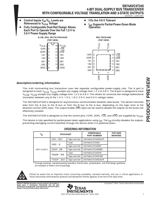
SN74AVC4T245RGYR中文资料
元器件交易网IMPORTANT NOTICETexas Instruments Incorporated and its subsidiaries (TI) reserve the right to make corrections, modifications,enhancements, improvements, and other changes to its products and services at any time and to discontinueany product or service without notice. Customers should obtain the latest relevant information before placingorders and should verify that such information is current and complete. All products are sold subject to TI’s termsand conditions of sale supplied at the time of order acknowledgment.TI warrants performance of its hardware products to the specifications applicable at the time of sale inaccordance with TI’s standard warranty. T esting and other quality control techniques are used to the extent TIdeems necessary to support this warranty. Except where mandated by government requirements, testing of allparameters of each product is not necessarily performed.TI assumes no liability for applications assistance or customer product design. Customers are responsible fortheir products and applications using TI components. T o minimize the risks associated with customer productsand applications, customers should provide adequate design and operating safeguards.TI does not warrant or represent that any license, either express or implied, is granted under any TI patent right,copyright, mask work right, or other TI intellectual property right relating to any combination, machine, or processin which TI products or services are used. Information published by TI regarding third-party products or servicesdoes not constitute a license from TI to use such products or services or a warranty or endorsement thereof.Use of such information may require a license from a third party under the patents or other intellectual propertyof the third party, or a license from TI under the patents or other intellectual property of TI.Reproduction of information in TI data books or data sheets is permissible only if reproduction is withoutalteration and is accompanied by all associated warranties, conditions, limitations, and notices. Reproductionof this information with alteration is an unfair and deceptive business practice. TI is not responsible or liable forsuch altered documentation.Resale of TI products or services with statements different from or beyond the parameters stated by TI for thatproduct or service voids all express and any implied warranties for the associated TI product or service andis an unfair and deceptive business practice. TI is not responsible or liable for any such statements.Following are URLs where you can obtain information on other Texas Instruments products and applicationsolutions:Products ApplicationsAmplifiers Audio /audioData Converters Automotive /automotiveDSP Broadband /broadbandInterface Digital Control /digitalcontrolLogic Military /militaryPower Mgmt Optical Networking /opticalnetworkMicrocontrollers Security /securityTelephony /telephonyVideo & Imaging /videoWireless /wirelessMailing Address:Texas InstrumentsPost Office Box 655303 Dallas, Texas 75265Copyright 2004, Texas Instruments Incorporated。
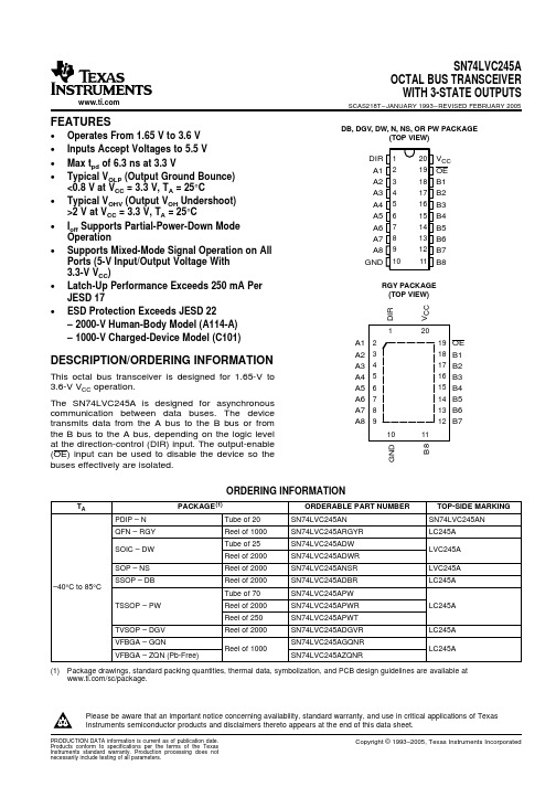
SN74LVC245APWR中文资料

Continuous current through VCC or GND
DB package(4)
DGV package (4)
DW package (4)
θJA
Package thermal impedance
GQN/ZQN package(4) N package(4)
NS package(4)
PRODUCTION DATA information is current as of publication date. Products conform to specifications per the terms of the Texas Instruments standard warranty. Production processing does not necessarily include testing of all parameters.
over operating free-air temperature range (unless otherwise noted)
VCC
Supply voltage range
VI
Input voltage range(2)
VO
Voltage range applied to any output in the high-impedance or power-off state(2)
SN74LVC245ADBR
Tube of 70
SN74LVC245APW
TSSOP – PW
Reel of 2000
SN74LVC245APWR
Reel of 250
SN74LVC245APWT
TVSOP – DGV
74AVC8T245 8位数据双向电平转换IC
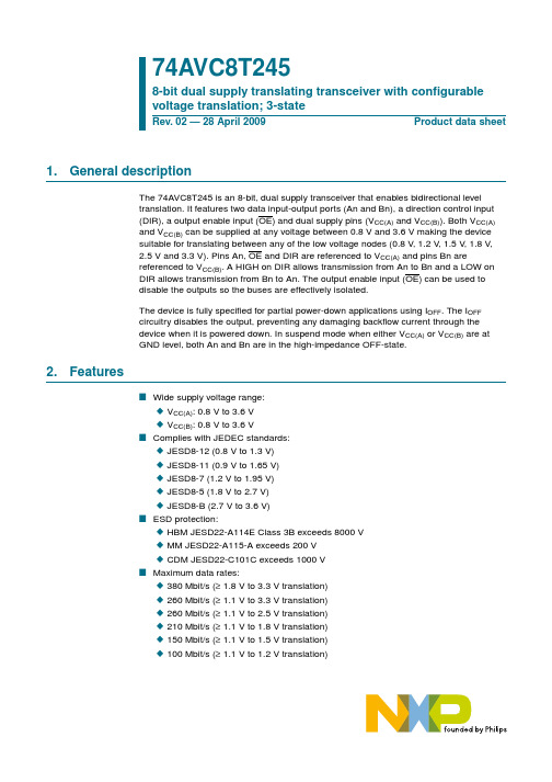
Supply voltage
Input
VCC(A), VCC(B) 0.8 V to 3.6 V
OE[2] L
0.8 V to 3.6 V
L
0.8 V to 3.6 V
H
GND[3]
X
DIR[2] L H X X
Input/output[3] An[2] An = Bn input Z Z
[1] H = HIGH voltage level; L = LOW voltage level; X = don’t care; Z = high-impedance OFF-state. [2] The An, DIR and OE input circuit is referenced to VCC(A); The Bn input circuit is referenced to VCC(B). [3] If at least one of VCC(A) or VCC(B) is at GND level, the device goes into suspend mode.
NXP Semiconductors
74AVC8T245
8-bit dual supply translating transceiver; 3-state
I Suspend mode I Latch-up performance exceeds 100 mA per JESD 78 Class II I Inputs accept voltages up to 3.6 V I IOFF circuitry provides partial Power-down mode operation I Multiple package options I Specified from −40 °C to +85 °C and −40 °C to +125 °C
SN74LVC245ADBR中文资料
Isolation
LOGIC DIAGRAM (POSITIVE LOGIC)
1 DIR
19 OE
A1 2 18 B1
To Seven Other Channels Pin numbers shown are for the DB, DGV, DW, N, NS, PW, and RGY packages.
GND B8
SN74LVC245A OCTAL BUS TRANSCEIVER
WITH 3-STATE OUTPUTS
SCAS218T – JANUARY 1993 – REVISED FEBRUARY 2005
DB, DGV, DW, N, NS, OR PW PACKAGE (TOP VIEW)
over operating free-air temperature range (unless otherwise noted)
VCC
Supply voltage range
VI
Input voltage range(2)
VO
Voltage range applied to any output in the high-impedance or power-off state(2)
VO
Voltage range applied to any output in the high or low state(2)(3)
IIK
Input clamp current
VI < 0
IOK
Output clamp current
VO < 0
IO
Continuous output current
74HC245中文资料,74HC245N规格书,74HC245D技术文档,DATASHEET,NXP代理商
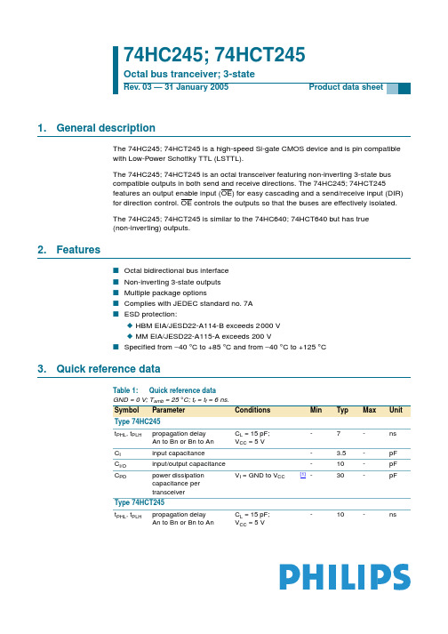
74HC245; 74HCT245
Octal bus tranceiver; 3-state
Rev. 03 — 31 January 2005
Product data sheet
1. General description
The 74HC245; 74HCT245 is a high-speed Si-gate CMOS device and is pin compatible with Low-Power Schottky TTL (LSTTL).
plastic shrink small outline package; 20 leads; body width 5.3 mm
SOT339-1
74HCT245BQ
−40 °C to +125 °C
DHVQFN20 plastic dual-in-line compatible thermal enhanced SOT764-1 very thin quad flat package no leads; 20 terminals; body 2.5 × 4.5 × 0.85 mm
x HBM EIA/JESD22-A114-B exceeds 2000 V x MM EIA/JESD22-A115-A exceeds 200 V s Specified from −40 °C to +85 °C and from −40 °C to +125 °C
3. Quick reference data
SOT163-1
74HCT245PW
−40 °C to +125 °C TSSOP20 plastic thin shrink small outline package; 20 leads; SOT360-1 body width 4.4 mm
HD74HC245RPEL中文资料
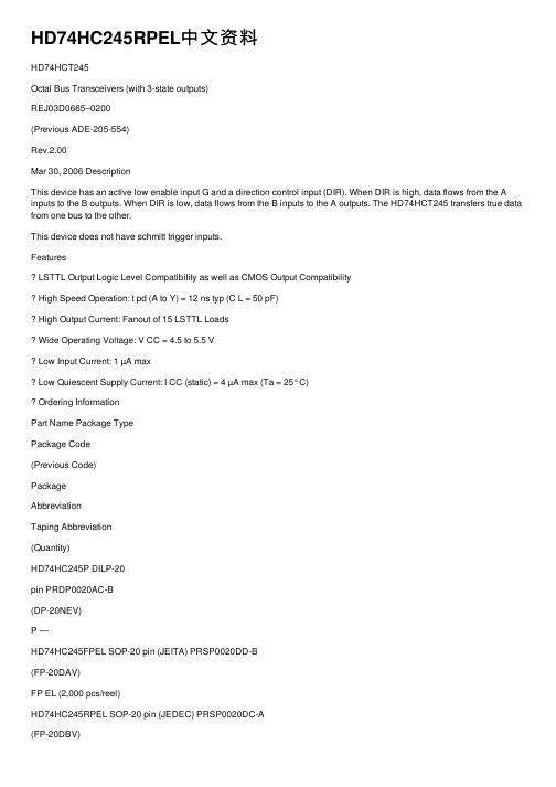
HD74HC245RPEL中⽂资料HD74HCT245Octal Bus Transceivers (with 3-state outputs)REJ03D0665–0200(Previous ADE-205-554)Rev.2.00Mar 30, 2006 DescriptionThis device has an active low enable input G and a direction control input (DIR). When DIR is high, data flows from the A inputs to the B outputs. When DIR is low, data flows from the B inputs to the A outputs. The HD74HCT245 transfers true data from one bus to the other.This device does not have schmitt trigger inputs.FeaturesLSTTL Output Logic Level Compatibility as well as CMOS Output CompatibilityHigh Speed Operation: t pd (A to Y) = 12 ns typ (C L = 50 pF)High Output Current: Fanout of 15 LSTTL LoadsWide Operating Voltage: V CC = 4.5 to 5.5 VLow Input Current: 1 µA maxLow Quiescent Supply Current: I CC (static) = 4 µA max (Ta = 25°C)Ordering InformationPart Name Package TypePackage Code(Previous Code)PackageAbbreviationTaping Abbreviation(Quantity)HD74HC245P DILP-20pin PRDP0020AC-B(DP-20NEV)P —HD74HC245FPEL SOP-20 pin (JEITA) PRSP0020DD-B(FP-20DAV)FP EL (2,000 pcs/reel)HD74HC245RPEL SOP-20 pin (JEDEC) PRSP0020DC-A(FP-20DBV)RP EL (1,000 pcs/reel)HD74HC245TELL TSSOP-20pin PTSP0020JB-A(TTP-20DAV)T ELL (2,000 pcs/reel)Note: Please consult the sales office for the above package availability. Function TableEnable G Direction Control DIR OperationL L B data to A busL H A data to B busH XIsolation H : high levelL : low levelX : irrelevantPin ArrangementAbsolute Maximum RatingsUnitRatingsItem SymbolSupply voltage range V CC–0.5 to 7.0 VInput / Output voltage V IN, V OUT–0.5 to V CC +0.5 VInput / Output diode current I IK, I OK±20 mA Output current I O±35 mA V CC, GND current I CC or I GND±75 mAmW Power dissipation P T 500Storage temperature Tstg –65 to +150 °CNote: The absolute maximum ratings are values, which must not individually be exceeded, and furthermore, no two of which may be realized at the same time.Recommended Operating ConditionsUnitConditionsRatingsItem SymbolSupply voltage V CC 4.5 to 5.5 VInput / Output voltage V IN, V OUT0 to V CC VOperating temperature Ta –40 to 85 °CInput rise / fall time*1t r, t f0 to 500 ns V CC = 4.5 VNotes: 1. This item guarantees maximum limit when one input switches.Waveform: Refer to test circuit of switching characteristics.Electrical CharacteristicsTa = 25°C Ta = –40 to+85°CItem Symbol V CC (V)Min Typ Max Min MaxUnit Test ConditionsV IH 4.5 to 5.5 2.0 — — 2.0 — V Input voltage V IL 4.5 to 5.5 — — 0.8 — 0.8 V 4.4 — — 4.4 — V I OH = –20 µAV OH 4.5 4.5 4.18 — — 4.13 — Vin = V IH or V IL I OH = –6 mA— — 0.1 — 0.1 V I OL = 20 µAOutput voltageV OL 4.5 4.5 — — 0.26 — 0.33 Vin = V IH or V IL I OL = 6 mAOff-state outputcurrentI OZ 5.5— — ±0.5 — ±5.0 µA Vin = V IH or V IL , Vout = V CC or GNDInput currentIin 5.5 — — ±0.1 — ±1.0 µA Vin = V CC or GND Quiescent current I CC 5.5 — — 4.0 — 40 µA Vin = V CC or GND, Iout = 0µASwitching Characteristics(C L = 50 pF, Input t r = t f = 6 ns)Ta = 25°CTa = –40 to +85°CItem Symbol V CC (V)Min Typ Max Min MaxUnit Test Conditionst PLH 4.5 — 11 22 —28 Propagation delay time t PHL 4.5 — 13 22 — 28 ns t ZL 4.5 — 17 30 — 38 Output enable time t ZH 4.5 — 14 30 — 38 ns t LZ 4.5 — 20 30 — 38 Output disable time t HZ 4.5 — 22 30 — 38ns Output rise/fall time t TLH t THL 4.5 — 4 12 — 15 ns Input capacitance Cin——510—10pFTest CircuitWaveformsPackage Dimensions/doc/9c8b776d27d3240c8547ef02.html RENESAS SALES OFFICESRefer to "/doc/9c8b776d27d3240c8547ef02.html /en/network" for the latest and detailed information. Renesas Technology America, Inc.450 Holger Way, San Jose, CA 95134-1368, U.S.ATel: <1> (408) 382-7500, Fax: <1> (408) 382-7501Renesas Technology Europe LimitedDukes Meadow, Millboard Road, Bourne End, Buckinghamshire, SL8 5FH, U.K.Tel: <44> (1628) 585-100, Fax: <44> (1628) 585-900Renesas Technology (Shanghai) Co., Ltd.Unit 204, 205, AZIACenter, No.1233 Lujiazui Ring Rd, Pudong District, Shanghai, China 200120Tel: <86> (21) 5877-1818, Fax: <86> (21) 6887-7898Renesas Technology Hong Kong Ltd.7th Floor, North Tower, World Finance Centre, Harbour City, 1 Canton Road, Tsimshatsui, Kowloon, Hong KongTel: <852> 2265-6688, Fax: <852> 2730-6071Renesas Technology Taiwan Co., Ltd.10th Floor, No.99, Fushing North Road, Taipei, TaiwanTel: <886> (2) 2715-2888, Fax: <886> (2) 2713-2999Renesas Technology Singapore Pte. Ltd.1 Harbour Front Avenue, #06-10, Keppel Bay Tower, Singapore 098632Tel: <65> 6213-0200, Fax: <65> 6278-8001Renesas Technology Korea Co., Ltd.Kukje Center Bldg. 18th Fl., 191, 2-ka, Hangang-ro, Yongsan-ku, Seoul 140-702, KoreaTel: <82> (2) 796-3115, Fax: <82> (2) 796-2145Renesas Technology Malaysia Sdn. BhdUnit 906, Block B, Menara Amcorp, Amcorp Trade Centre, No.18, Jalan Persiaran Barat, 46050 Petaling Jaya, Selangor Darul Ehsan, MalaysiaTel: <603> 7955-9390, Fax: <603> 7955-95102006. Renesas Technology Corp., All rights reserved. Printed in Japan.。
TC74ACT245P资料
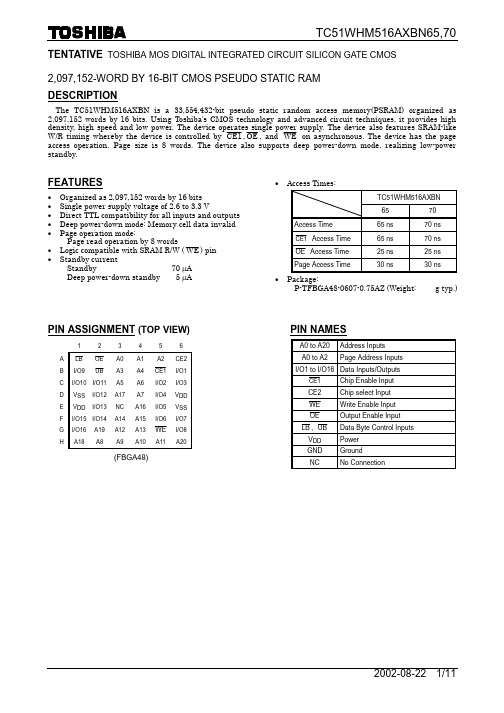
FEATURES
• • • • • • • Organized as 2,097,152 words by 16 bits Single power supply voltage of 2.6 to 3.3 V Direct TTL compatibility for all inputs and outputs Deep power-down mode: Memory cell data invalid Page operation mode: Page read operation by 8 words Logic compatible with SRAM R/W ( WE ) pin Standby current Standby 70 µA Deep power-down standby 5 µA
* : VIH(Max) VDD+1.0 V with 10 ns pulse width VIL(Min) -1.0 V with 10 ns pulse width
DC CHARACTERISTICS (Ta = −25°C to 85°C, VDD = 2.6 to 3.3 V) (See Note 3 to 4)
MAX +1.0 +1.0 0.4 40
UNIT µA µA V V mA
Page Access Operating Current Standby Current(MOS) Deep Power-down Standby Current
25 70 5
mA µA µA
CE1 = VDD − 0.2 V, CE2 = VDD − 0.2 V
CE2 WE
OE
I/O15 I/O14 I/O16 A18 A19 A8
74xx245中文资料
74
Vcc=最大
VI=5.5V VI=7V
Vcc=最大,VIH=2.7V
IIL输入低电平电流
Vcc=最大,VIL=0.4V
IOS输出短路电流 IOZH输出高阻态时高
电平电流 IOZL输出高阻态时低
电平电流
Icc 电源电流
Vcc=最大
Vcc=最大,VIH=2V VIL=最大,VO=2.7V Vcc=最大,VIH=2V,VIL=最大
5
5.5
4.75
5
5.25
2
0.7 0.8 -12 -15
12 24
单位 V V V mA mA
参
数
tPLH输出由低到高传输延迟时间 tPHL输出由高到低传输延迟时间 tPZH输出由高阻态到高允许时间 tPZL输出由高阻态到低允许时间 tPHZ输出由高到高阻态禁止时间 tPLZ输出由低到高阻态禁止时间
54/74245
双向总线发送器/接收器(3S)
简要说明: 245 为三态输出的八组总线收发器,其主要电器特性的典型值如下(不同厂家
具体值有差别):
型号
tPLH
54LS245/74LS245
8ns
tphl
PD
8ns
275mW
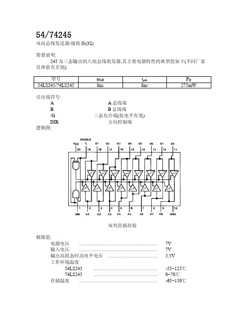
引出端符号: A B /G DIR
逻辑图:
A 总线端 B 总线端 三态允许端(低电平有效) 方向控制端
测试条件
Vcc =5V CL=45pF RL=667 Ω
Vcc=5V CL=5pF RL=90 Ω
静态特性(TA 为工作环境温度范围)
LS245 最大
12 12 40 40 25 25
单位
ns ns ns ns ns nsቤተ መጻሕፍቲ ባይዱ
74AVC4T245QRGYRQ1;中文规格书,Datasheet资料
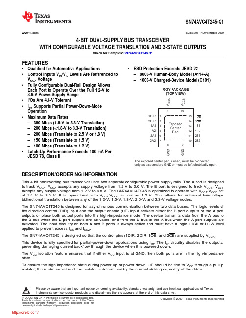
GNCBGNCARGY PACKAGE(TOP VIEW)The exposed center pad, if used, must be connectedonly as a secondary GND or must be left electrically open.SN74AVC4T245-Q1 SCES792–NOVEMBER20094-BIT DUAL-SUPPLY BUS TRANSCEIVERWITH CONFIGURABLE VOLTAGE TRANSLATION AND3-STATE OUTPUTSCheck for Samples:SN74AVC4T245-Q1FEATURES•Qualified for Automotive Applications•ESD Protection Exceeds JESD22•Control Inputs V IH/V IL Levels Are Referenced to–8000-V Human-Body Model(A114-A) V CCA Voltage–1000-V Charged-Device Model(C101)•Fully Configurable Dual-Rail Design AllowsEach Port to Operate Over the Full1.2-V to3.6-V Power-Supply Range•I/Os Are4.6-V Tolerant•I off Supports Partial Power-Down-ModeOperation•Maximum Data Rates–380Mbps(1.8-V to3.3-V Translation)–200Mbps(<1.8-V to3.3-V Translation)–200Mbps(Translate to2.5V or1.8V)–150Mbps(Translate to1.5V)–100Mbps(Translate to1.2V)•Latch-Up Performance Exceeds100mA PerJESD78,Class IIDESCRIPTION/ORDERING INFORMATIONThis4-bit noninverting bus transceiver uses two separate configurable power-supply rails.The A port is designed to track V CCA.V CCA accepts any supply voltage from1.2V to3.6V.The B port is designed to track V CCB.V CCB accepts any supply voltage from1.2V to3.6V.The SN74AVC4T245is optimized to operate with V CCA/V CCB set at 1.4V to 3.6V.It is operational with V CCA/V CCB as low as 1.2V.This allows for universal low-voltage bidirectional translation between any of the1.2-V,1.5-V,1.8-V,2.5-V,and3.3-V voltage nodes.The SN74AVC4T245is designed for asynchronous communication between two data buses.The logic levels of the direction-control(DIR)input and the output-enable(OE)input activate either the B-port outputs or the A-port outputs or place both output ports into the high-impedance mode.The device transmits data from the A bus to the B bus when the B-port outputs are activated,and from the B bus to the A bus when the A-port outputs are activated.The input circuitry on both A and B ports is always active and must have a logic HIGH or LOW level applied to prevent excess I CC and I CCZ.The SN74AVC4T245is designed so that the control pins(1DIR,2DIR,and are supplied by V CCA. This device is fully specified for partial-power-down applications using I off.The I off circuitry disables the outputs, preventing damaging current backflow through the device when it is powered down.The V CC isolation feature ensures that if either V CC input is at GND,then both ports are in the high-impedance state.To ensure the high-impedance state during power up or power down,OE should be tied to V CC through a pullup resistor;the minimum value of the resistor is determined by the current-sinking capability of the driver.Please be aware that an important notice concerning availability,standard warranty,and use in critical applications of TexasInstruments semiconductor products and disclaimers thereto appears at the end of this data sheet.PRODUCTION DATA information is current as of publication date.Copyright©2009,Texas Instruments Incorporated Products conform to specifications per the terms of the TexasInstruments standard warranty.Production processing does notnecessarily include testing of all parameters.DIROE A1A2B1B2SN74AVC4T245-Q1SCES792–ORDERING INFORMATION(1)T A PACKAGE(2)ORDERABLE PART NUMBER TOP-SIDE MARKING –40°C to125°C QFN–RGY Reel of100074AVC4T245QRGYRQ14T245Q(1)For the most current package and ordering information,see the Package Option Addendum at the end of this document,or see the TIweb site at .(2)Package drawings,thermal data,and symbolization are available at /packaging.Table1.FUNCTION TABLE(1)(each2-bit section)CONTROL INPUTS OUTPUT CIRCUITSOPERATIONOE DIR A PORT B PORTL L Enabled Hi-Z B data to A busL H Hi-Z Enabled A data to B busH X Hi-Z Hi-Z Isolation(1)Input circuits of the data I/Os are always active.LOGIC DIAGRAM(POSITIVE LOGIC)FOR1/2OF AVC4T2452Submit Documentation Feedback Copyright©2009,Texas Instruments IncorporatedProduct Folder Link(s):SN74AVC4T245-Q1SN74AVC4T245-Q1 SCES792–NOVEMBER2009ABSOLUTE MAXIMUM RATINGS(1)over operating free-air temperature range(unless otherwise noted)MIN MAX UNITV CCASupply voltage range–0.5 4.6VV CCBI/O ports(A port)–0.5 4.6V I Input voltage range(2)I/O ports(B port)–0.5 4.6VControl inputs–0.5 4.6A port–0.5 4.6Voltage range applied to any output in the high-impedance orV O V power-off state(2)B port–0.5 4.6A port–0.5V CCA+0.5V O Voltage range applied to any output in the high or low state(2)(3)VB port–0.5V CCB+0.5I IK Input clamp current V I<0–50mAI OK Output clamp current V O<0–50mAI O Continuous output current±50mAContinuous current through V CCA,V CCB,or GND±100mAq JA Package thermal impedance RGY package(4)39°C/WT stg Storage temperature range–65150°C (1)Stresses beyond those listed under"absolute maximum ratings"may cause permanent damage to the device.These are stress ratingsonly,and functional operation of the device at these or any other conditions beyond those indicated under"recommended operating conditions"is not implied.Exposure to absolute-maximum-rated conditions for extended periods may affect device reliability.(2)The input voltage and output negative-voltage ratings may be exceeded if the input and output current ratings are observed.(3)The output positive-voltage rating may be exceeded up to4.6V maximum if the output current rating is observed.(4)The package thermal impedance is calculated in accordance with JESD51-5.Copyright©2009,Texas Instruments Incorporated Submit Documentation Feedback3Product Folder Link(s):SN74AVC4T245-Q1SN74AVC4T245-Q1SCES792–RECOMMENDED OPERATING CONDITIONS(1)(2)(3)V CCI V CCO MIN MAX UNIT V CCA Supply voltage 1.2 3.6VV CCB Supply voltage 1.2 3.6V1.2V to1.95V V CCI×0.65High-levelV IH Data inputs(4) 1.95V to2.7V 1.6V input voltage2.7V to3.6V21.2V to1.95V V CCI×0.35Low-levelV IL Data inputs(4) 1.95V to2.7V0.7V input voltage2.7V to3.6V0.81.2V to1.95V V CCA×0.65High-level DIRV IH 1.95V to2.7V 1.6V input voltage(referenced to V CCA)(5)2.7V to3.6V21.2V to1.95V V CCA×0.35Low-level DIRV IL 1.95V to2.7V0.7V input voltage(referenced to V CCA)(5)2.7V to3.6V0.8V I Input voltage0 3.6VActive state0V CCOV O Output voltage V3-state0 3.61.2V–31.4V to1.6V–6I OH High-level output current 1.65V to1.95V–8mA2.3V to2.7V–93V to3.6V–121.1V to1.2V31.4V to1.6V6I OL Low-level output current 1.65V to1.95V8mA2.3V to2.7V93V to3.6V12Δt/Δv Input transition rise or fall rate5ns/VT A Operating free-air temperature–40125°C(1)V CCI is the V CC associated with the input port.(2)V CCO is the V CC associated with the output port.(3)All unused data inputs of the device must be held at V CCI or GND to ensure proper device operation.Refer to the TI application report,Implications of Slow or Floating CMOS Inputs,literature number SCBA004.(4)For V CCI values not specified in the data sheet,V IH min=V CCI×0.7V,V IL max=V CCI×0.3V(5)For V CCI values not specified in the data sheet,V IH min=V CCA×0.7V,V IL max=V CCA×0.3V4Submit Documentation Feedback Copyright©2009,Texas Instruments IncorporatedProduct Folder Link(s):SN74AVC4T245-Q1SN74AVC4T245-Q1 SCES792–NOVEMBER2009ELECTRICAL CHARACTERISTICS(1)(2)over recommended operating free-air temperature range(unless otherwise noted)T A=25°C–40°C to125°C PARAMETER TEST CONDITIONS V CCA V CCB UNITMIN TYP MAX MIN MAXI OH=–100m A 1.2V to3.6V 1.2V to3.6V V CCO–0.2I OH=–3mA 1.2V 1.2V0.95I OH=–6mA 1.4V 1.4V 1.05V OH V I=V IH VI OH=–8mA 1.65V 1.65V 1.2I OH=–9mA 2.3V 2.3V 1.75I OH=–12mA3V3V 2.3I OL=100m A 1.2V to3.6V 1.2V to3.6V0.2I OL=3mA 1.2V 1.2V0.25I OL=6mA 1.4V 1.4V0.35V OL V I=V IL VI OL=8mA 1.65V 1.65V0.45I OL=9mA 2.3V 2.3V0.55I OL=12mA3V3V0.7ControlI I(3)V I=V CCA or GND 1.2V to3.6V 1.2V to3.6V±0.025±0.25±1.5m Ainputs0V0V to3.6V±0.1±1±5I off A or B port V I or V O=0to3.6V m A0V to3.6V0V±0.1±1±5V O=V CCO or GND,I OZ A or B port 3.6V 3.6V±0.5±2.5±5m AV I=V CCI or GND,OE=V IH1.2V to3.6V 1.2V to3.6V8I CCA(3)V I=V CCI or GND,I O=00V0V to3.6V–2–11m A0V to3.6V0V81.2V to3.6V 1.2V to3.6V8I CCB(3)V I=V CCI or GND,I O=00V0V to3.6V8m A0V to3.6V0V–2–11I CCA+I CCB V I=V CCI or GND,I O=0 1.2V to3.6V 1.2V to3.6V16m AControlC i V I=3.3V or GND 3.3V 3.3V 3.5 4.5pFinputsC io A or B port V O=3.3V or GND 3.3V 3.3V67pF(1)V CCO is the V CC associated with the output port.(2)V CCI is the V CC associated with the input port.(3)All unused data inputs of the device must be held at V CCI or GND to ensure proper device operation.Refer to the TI application report,Implications of Slow or Floating CMOS Inputs,literature number SCBA004.Copyright©2009,Texas Instruments Incorporated Submit Documentation Feedback5Product Folder Link(s):SN74AVC4T245-Q1SN74AVC4T245-Q1SCES792–SWITCHING CHARACTERISTICSover recommended operating free-air temperature range,V CCA=1.2V(unless otherwise noted)(see Figure1)V CCB=1.5V V CCB=1.8V V CCB=2.5V V CCB=3.3VV CCB=1.2VFROM TO±0.1V±0.15V±0.2V±0.3V PARAMETER UNIT (INPUT)(OUTPUT)TYP TYP TYP TYP TYPt PLH 3.4 2.9 2.7 2.6 2.8A B nst PHL 3.4 2.9 2.7 2.6 2.8t PLH 3.6 3.1 2.8 2.6 2.6B A nst PHL 3.6 3.1 2.8 2.6 2.6t PZH 5.6 4.7 4.3 3.9 3.7OE A ns t PZL 5.6 4.7 4.3 3.9 3.7t PZH5 4.3 3.9 3.636.6OE B ns t PZL5 4.3 3.9 3.6 3.6t PHZ 6.2 5.2 5.2 4.3 4.8OE A ns t PLZ 6.2 5.2 5.2 4.3 4.8t PHZ 5.9 5.15 4.7 5.5OE B ns t PLZ 5.9 5.15 4.7 5.5SWITCHING CHARACTERISTICSover recommended operating free-air temperature range,V CCA=1.5V±0.1V(see Figure1)V CCB=1.5V V CCB=1.8V V CCB=2.5V V CCB=3.3VV CCB=1.2VFROM TO±0.1V±0.15V±0.2V±0.3V PARAMETER UNIT (INPUT)(OUTPUT)TYP MIN MAX MIN MAX MIN MAX MIN MAXt PLH 3.211.310.29.29.2A B nst PHL 3.211.310.29.29.2t PLH 3.311.31110.710.6B A nst PHL 3.311.31110.710.6t PZH 4.914.614.514.414.4 OE A ns t PZL 4.914.614.514.414.4t PZH 4.514.612.710.810.6 OE B ns t PZL 4.514.612.710.810.6t PHZ 5.615.215.215.215.2 OE A ns t PLZ 5.615.215.215.215.2t PHZ 5.215.314.112.412.6 OE B ns t PLZ 5.215.314.112.412.66Submit Documentation Feedback Copyright©2009,Texas Instruments IncorporatedProduct Folder Link(s):SN74AVC4T245-Q1SN74AVC4T245-Q1 SCES792–NOVEMBER2009SWITCHING CHARACTERISTICSover recommended operating free-air temperature range,V CCA=1.8V±0.15V(see Figure1)V CCB=1.5V V CCB=1.8V V CCB=2.5V V CCB=3.3VV CCB=1.2VFROM TO±0.1V±0.15V±0.2V±0.3V PARAMETER UNIT (INPUT)(OUTPUT)TYP MIN MAX MIN MAX MIN MAX MIN MAXt PLH 2.9119.98.98.9A B nst PHL 2.9119.98.98.9t PLH310.39.99.69.5B A nst PHL310.39.99.69.5t PZH 4.412.412.312.312.2 OE A ns t PZL 4.412.412.312.312.2t PZH 4.114.212.410.39.6 OE B ns t PZL 4.114.212.410.39.6t PHZ 5.413.613.713.713.7 OE A ns t PLZ 5.413.613.713.713.7t PHZ514.913.711.911.9 OE B ns t PLZ514.913.711.911.9SWITCHING CHARACTERISTICSover recommended operating free-air temperature range,V CCA=2.5V±0.2V(see Figure1)V CCB=1.5V V CCB=1.8V V CCB=2.5V V CCB=3.3VV CCB=1.2VFROM TO±0.1V±0.15V±0.2V±0.3V PARAMETER UNIT (INPUT)(OUTPUT)TYP MIN MAX MIN MAX MIN MAX MIN MAXt PLH 2.810.79.68.58.6A B nst PHL 2.810.79.68.58.6t PLH 2.79.28.98.48.3B A nst PHL 2.79.28.98.48.3t PZH411.510.29.89.8 OE A ns t PZL411.510.29.89.8t PZH 3.813.8129.89 OE B ns t PZL 3.813.8129.89t PHZ 4.713.413.411.211.6 OE A ns t PLZ 4.713.413.411.211.6t PHZ 4.514.413.211.210.2 OE B ns t PLZ 4.514.413.211.210.2Copyright©2009,Texas Instruments Incorporated Submit Documentation Feedback7Product Folder Link(s):SN74AVC4T245-Q1SN74AVC4T245-Q1SCES792–SWITCHING CHARACTERISTICSover recommended operating free-air temperature range,V CCA=3.3V±0.3V(see Figure1)V CCB=1.5V V CCB=1.8V V CCB=2.5V V CCB=3.3VV CCB=1.2VFROM TO±0.1V±0.15V±0.2V±0.3V PARAMETER UNIT (INPUT)(OUTPUT)TYP MIN MAX MIN MAX MIN MAX MIN MAXt PLH 2.910.69.58.37.9A B nst PHL 2.910.69.58.37.9t PLH 2.69.28.487.8B A nst PHL 2.69.28.487.8t PZH 3.813.710.28.88.8 OE A ns t PZL 3.813.710.28.88.8t PZH 3.713.711.89.78.8 OE B ns t PZL 3.713.711.89.78.8t PHZ 4.814.313.310.611.6 OE A ns t PLZ 4.814.313.310.611.6t PHZ 5.314.313.111.411.2 OE B ns t PLZ 5.314.313.111.411.2OPERATING CHARACTERISTICST A=25°CV CCA=V CCA=V CCA=V CCA=V CCA=TEST VCCB =1.2V V CCB=1.5V V CCB=1.8V V CCB=2.5V V CCB=3.3VPARAMETER UNIT CONDITIONSTYP TYP TYP TYP TYPOutputs111 1.52 enabledA to BOutputs11111C L=0,disabledC pdA(1)f=10MHz,pFOutputs tr =t f=1ns1212.5131415enabledB to AOutputs11111 disabledOutputs1212.5131415 enabledA to BOutputs11111C L=0,disabledC pdB(1)f=10MHz,pFOutputs tr =t f=1ns11112enabledB to AOutputs11111 disabled(1)Power dissipation capacitance per transceiver8Submit Documentation Feedback Copyright©2009,Texas Instruments IncorporatedProduct Folder Link(s):SN74AVC4T245-Q1V OH V OLLOAD CIRCUIT × V CCOOpenOutput Control (low-level enabling)Output Waveform 1S1 at 2 × V CCO (see Note B)Output Waveform 2S1 at GND (see Note B)0 V0 VV CCI0 VV CCAV CCOVOLTAGE WAVEFORMS PROPAGATION DELAY TIMESVOLTAGE WAVEFORMS PULSE DURATIONVOLTAGE WAVEFORMS ENABLE AND DISABLE TIMESInputt pd t PLZ /t PZL t PHZ /t PZHOpen 2 × V CCO GNDTEST S1NOTES: A.C L includes probe and jig capacitance.B.Waveform 1 is for an output with internal conditions such that the output is low, except when disabled by the output control.Waveform 2 is for an output with internal conditions such that the output is high, except when disabled by the output control.C.All input pulses are supplied by generators having the following characteristics: PRR v 10 MHz, Z O = 50 Ω, dv/dt ≥ 1 V/ns.D.The outputs are measured one at a time, with one transition per measurement.E.t PLZ and t PHZ are the same as t dis .F.t PZL and t PZH are the same as t en .G.t PLH and t PHL are the same as t pd .H.V CCI is the V CC associated with the input port.I.V CCO is the V CC associated with the output port.1.2 V 1.5 V ± 0.1 V 1.8 V ± 0.15 V2.5 V ± 0.2 V3.3 V ± 0.3 V2 k Ω2 k Ω2 k Ω2 k Ω2 k ΩV CCO R L 0.1 V 0.1 V 0.15 V 0.15 V 0.3 VV TP C L 15 pF 15 pF 15 pF 15 pF 15 pFSN74AVC4T245-Q1SCES792–NOVEMBER 2009PARAMETER MEASUREMENT INFORMATIONFigure 1.Load and Circuit and Voltage WaveformsCopyright ©2009,Texas Instruments Incorporated Submit Documentation Feedback9Product Folder Link(s):SN74AVC4T245-Q1PACKAGAddendum-Page 1PACKAGING INFORMATIONOrderable Device Status(1)Package Type PackageDrawingPins Package QtyEco Plan(2)Lead/Ball FinishMSL Pea74AVC4T245QRGYRQ1ACTIVEVQFNRGY163000Green (RoHS & no Sb/Br)CU NIPDAU Level-3-260C(1)The marketing status values are defined as follows:ACTIVE: Product device recommended for new designs.LIFEBUY: TI has announced that the device will be discontinued, and a lifetime-buy period is in effect.NRND: Not recommended for new designs. Device is in production to support existing customers, but TI does not recommend using this part in a new PREVIEW: Device has been announced but is not in production. Samples may or may not be available.OBSOLETE: TI has discontinued the production of the device.(2)Eco Plan - The planned eco-friendly classification: Pb-Free (RoHS), Pb-Free (RoHS Exempt), or Green (RoHS & no Sb/Br) - please check http://www.t information and additional product content details.TBD: The Pb-Free/Green conversion plan has not been defined.Pb-Free (RoHS): TI's terms "Lead-Free" or "Pb-Free" mean semiconductor products that are compatible with the current RoHS requirements for all lead not exceed 0.1% by weight in homogeneous materials. Where designed to be soldered at high temperatures, TI Pb-Free products are suitable fo Pb-Free (RoHS Exempt): This component has a RoHS exemption for either 1) lead-based flip-chip solder bumps used between the die and package, the die and leadframe. The component is otherwise considered Pb-Free (RoHS compatible) as defined above.Green (RoHS & no Sb/Br): TI defines "Green" to mean Pb-Free (RoHS compatible), and free of Bromine (Br) and Antimony (Sb) based flame retard in homogeneous material)(3)MSL, Peak Temp. -- The Moisture Sensitivity Level rating according to the JEDEC industry standard classifications, and peak solder temperature.Important Information and Disclaimer:The information provided on this page represents TI's knowledge and belief as of the date that it is provided. TI provided by third parties, and makes no representation or warranty as to the accuracy of such information. Efforts are underway to better integrate inf continues to take reasonable steps to provide representative and accurate information but may not have conducted destructive testing or chemical an TI and TI suppliers consider certain information to be proprietary, and thus CAS numbers and other limited information may not be available for releasIn no event shall TI's liability arising out of such information exceed the total purchase price of the TI part(s) at issue in this document sold by TI to CuOTHER QUALIFIED VERSIONS OF SN74AVC4T245-Q1 :•Catalog: SN74AVC4T245NOTE: Qualified Version Definitions:•Catalog - TI's standard catalog product/分销商库存信息:TI74AVC4T245QRGYRQ1。
4LVTH245WM,74LVTH245WMX,74LVTH245SJ,74LVTH245SJX,74LVTH245MSA,74LVTH245MSAX, 规格书,Datasheet 资料
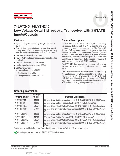
Order Number PackageNumber Package Description74LVT245WM M20B20-Lead Small Outline Integrated Circuit (SOIC), JEDEC MS-013, 0.300" Wide 74LVT245SJ M20D20-Lead Small Outline Package (SOP), EIAJ TYPE II, 5.3mm Wide74LVT245MSA MSA2020-Lead Shrink Small Outline Package (SSOP), JEDEC MO-150, 5.3mm Wide 74LVT245MTC MTC2020-Lead Thin Shrink Small Outline Package (TSSOP), JEDEC MO-153, 4.4mmWide74LVTH245WM M20B20-Lead Small Outline Integrated Circuit (SOIC), JEDEC MS-013, 0.300" Wide 74LVTH245SJ M20D20-Lead Small Outline Package (SOP), EIAJ TYPE II, 5.3mm Wide74LVTH245MSA MSA2020-Lead Shrink Small Outline Package (SSOP), JEDEC MO-150, 5.3mm Wide 74LVTH245MTC MTC2020-Lead Thin Shrink Small Outline Package (TSSOP), JEDEC MO-153, 4.4mmWide74LVT245, 74LVTH245 — Low Voltage Octal Bidirectional Transceiver with 3-STATE Inputs/Outputs Low Voltage Octal Bidirectional Transceiver with 3-STATE Inputs/Outputs Features■Input and output interface capability to systems at 5V V CC■Bushold data inputs eliminate the need for external pull-up resistors to hold unused inputs (74LVTH245), also available without bushold feature (74LVT245)■Live insertion/extraction permitted■Power Up/Down high impedance provides glitch-free bus loading■Outputs source/sink, –32mA/+64mA ■Latch-up performance exceeds 500mA■ESD performance:– Human-body model > 2000V– Machine model > 200V– Charged-device model> 1000V General Description The LVT245 and LVTH245 contain eight non-inverting bidirectional buffers with 3-STATE outputs and are intended for bus-oriented applications. The Transmit/Receive (T/R) input determines the direction of data flow through the bidirectional transceiver. Transmit (active-HIGH) enables data from A ports to B ports; Receive(active-LOW) enables data from B ports to A ports. The Output Enable input, when HIGH, disables both A and B ports by placing them in a HIGH Z condition.The LVTH245 data inputs include bushold, eliminating the need for external pull-up resistors to hold unused inputs.These transceivers are designed for low-voltage (3.3V)V CC applications, but with the capability to provide a TTL interface to a 5V environment. The LVT245 and LVTH245 are fabricated with an advanced BiCMOS technology to achieve high speed operation similar to 5V ABT while maintaining a low power dissipation.Ordering Information Device also available in Tape and Reel. Specify by appending suffix letter “X” to the ordering number.74LVT245, 74LVTH245 — Low Voltage Octal Bidirectional Transceiver with 3-STATE Inputs/Outputs Pin Description IEEE/IEC Truth Table H = HIGH Voltage Level L = LOW Voltage Level X = Immaterial Pin Names Description OE Output Enable Input T/R Transmit/Receive Input A0–A7Side A Inputs or 3-STATE Outputs B0–B7Side B Inputs or 3-STATE Outputs Inputs Outputs OE T/R L L Bus B Data to Bus A L H Bus A Data to Bus B H X HIGH-Z State74LVT245, 74LVTH245 — Low Voltage Octal Bidirectional Transceiver with 3-STATE Inputs/Outputs Note:1.I O Absolute Maximum Rating must be observed.Recommended Operating Conditions The Recommended Operating Conditions table defines the conditions for actual device operation. Recommended operating conditions are specified to ensure optimal performance to the datasheet specifications. Fairchild does not recommend exceeding them or designing to absolute maximum ratings.V CC Supply Voltage–0.5V to +4.6V V I DC Input Voltage–0.5V to +7.0V V O DC Output Voltage Output in 3-STATE–0.5V to +7.0V Output in HIGH or LOW State(1)–0.5V to +7.0V I IK DC Input Diode Current, V I< GND–50mA I OK DC Output Diode Current, V O< GND–50mA I O DC Output Current, V O> V CC Output at HIGH State64mA Output at LOW State128mA I CC DC Supply Current per Supply Pin±64mA I GND DC Ground Current per Ground Pin±128mA T STG Storage Temperature–65°C to +150°C Symbol Parameter Min Max Units V CC Supply Voltage 2.7 3.6V V I Input Voltage0 5.5V I OH HIGH-Level Output Current –32mA I OL LOW-Level Output Current64mA T A Free-Air Operating Temperature –4085°C∆t/∆V Input Edge Rate, V IN= 0.8V–2.0V, V CC= 3.0V 010ns/V74LVT245, 74LVTH245 — Low Voltage Octal Bidirectional Transceiver with 3-STATE Inputs/OutputsNotes:2.Applies to Bushold versions only (LVTH245).3.An external driver must source at least the specified current to switch from LOW-to-HIGH. V O ≥ V CC – 0.1V V IL Input LOW Voltage 2.7–3.60.8V OHOutput HIGH Voltage2.7–3.6I OH = –100µA V CC – 0.2V2.7I OH = – 8mA 2.43.0I OH = –32mA 2.0V OLOutput LOW Voltage 2.7I OL = 100µA 0.2VI OL = 24mA 0.53.0I OL = 16mA 0.4I OL = 32mA 0.5I OL = 64mA0.55I I(HOLD)(2) Bushold Input Minimum Drive 3.0V I = 0.8V 75µA V I = 2.0V–75I I(OD)(2)Bushold Input Over-Drive,Current to Change State 3.0 (3) 500µA (4)–500I IInput Current3.6V I = 5.5V 10µAControl Pins 3.6V I = 0V or V CC ±1 Data Pins3.6V I = 0V –5V I = V CC1I OFF Power Off Leakage Current 00V ≤ V I or V O ≤ 5.5V ±100µA I PU/PD Power Up/Down, 3-STATE Current 0–1.5V V O = 0.5V to V CC , V I= GND to V CC ±100µA I OZL 3-STATE Output Leakage Current 3.6V O = 0.5V –5µA I OZL (2)3-STATE Output Leakage Current 3.6V O = 0.0V –5µA I OZH 3-STATE Output Leakage Current 3.6V O = 3.0V 5µA I OZH (2)3-STATE Output Leakage Current 3.6V O = 3.6V 5µA I OZH +3-STATE Output Leakage Current 3.6V CC < V O ≤ 5.5V 10µA I CCH Power Supply Current 3.6Outputs HIGH 0.19mA I CCL Power Supply Current 3.6Outputs LOW 5mA I CCZ Power Supply Current 3.6Outputs Disabled 0.19mA I CCZ +Power Supply Current3.6V CC ≤ V O ≤ 5.5V ,Outputs Disabled 0.19mA ∆I CCIncrease in Power Supply Current (5)3.6One Input at V CC – 0.6V , Other Inputs at V CC or GND0.2mAAlways visit Fairchild Semiconductor’s online packaging area for the most recent package drawings: /packaging/Figure 2. 20-Lead Small Outline Package (SOP), EIAJ TYPE II, 5.3mm WidePackage drawings are provided as a service to customers considering Fairchild components. Drawings may change in any manner without notice. Please note the revision and/or date on the drawing and contact a Fairchild Semiconductor representative to verify orFigure 3. 20-Lead Shrink Small Outline Package (SSOP), JEDEC MO-150, 5.3mm WidePackage drawings are provided as a service to customers considering Fairchild components. Drawings may change in any manner without notice. Please note the revision and/or date on the drawing and contact a Fairchild Semiconductor representative to verify or obtain the most recent revision. Package specifications do not expand the terms of Fairchild’s worldwide terms and conditions,Figure 4. 20-Lead Thin Shrink Small Outline Package (TSSOP), JEDEC MO-153, 4.4mm WidePackage drawings are provided as a service to customers considering Fairchild components. Drawings may change in any mannersubsidiaries,and is not intended to be an exhaustive list of all such trademarks.ACEx®Build it Now™CorePLUS™CROSSVOLT™CTL™Current Transfer Logic™EcoSPARK®EZSWITCH™*™®Fairchild®Fairchild Semiconductor®FACT Quiet Series™FACT®FAST®FastvCore™FlashWriter®*FPS™FRFET®Global Power Resource SMGreen FPS™Green FPS™e-Series™GTO™i-Lo™IntelliMAX™ISOPLANAR™MegaBuck™MICROCOUPLER™MicroFET™MicroPak™MillerDrive™Motion-SPM™OPTOLOGIC®OPTOPLANAR®®PDP-SPM™Power220®POWEREDGE®Power-SPM™PowerTrench®Programmable Active Droop™QFET®QS™QT Optoelectronics™Quiet Series™RapidConfigure™SMART START™SPM®STEALTH™SuperFET™SuperSOT™-3SuperSOT™-6SuperSOT™-8SupreMOS™SyncFET™®The Power Franchise®TinyBoost™TinyBuck™TinyLogic®TINYOPTO™TinyPower™TinyPWM™TinyWire™µSerDes™UHC®Ultra FRFET™UniFET™VCX™*EZSWITCH™and FlashWriter®are trademarks of System General Corporation,used under license by Fairchild Semiconductor.DISCLAIMERFAIRCHILD SEMICONDUCTOR RESERVES THE RIGHT TO MAKE CHANGES WITHOUT FURTHER NOTICE TO ANY PRODUCTS HEREIN TO IMPROVE RELIABILITY,FUNCTION,OR DESIGN.FAIRCHILD DOES NOT ASSUME ANY LIABILITY ARISING OUT OF THE APPLICATION OR USE OF ANY PRODUCT OR CIRCUIT DESCRIBED HEREIN;NEITHER DOES IT CONVEY ANY LICENSE UNDER ITS PATENT RIGHTS,NOR THE RIGHTS OF OTHERS.THESE SPECIFICATIONS DO NOT EXPAND THE TERMS OF FAIRCHILD’S WORLDWIDE TERMS AND CONDITIONS,SPECIFICALLY THE WARRANTY THEREIN,WHICH COVERS THESE PRODUCTS.LIFE SUPPORT POLICYFAIRCHILD’S PRODUCTS ARE NOT AUTHORIZED FOR USE AS CRITICAL COMPONENTS IN LIFE SUPPORT DEVICES OR SYSTEMS WITHOUT THE EXPRESS WRITTEN APPROVAL OF FAIRCHILD SEMICONDUCTOR CORPORATION.As used herein:1.Life support devices or systems are devices or systemswhich,(a)are intended for surgical implant into the body or(b)support or sustain life,and(c)whose failure to performwhen properly used in accordance with instructions for use provided in the labeling,can be reasonably expected to result in a significant injury of the user.2.A critical component in any component of a life support,device,or system whose failure to perform can be reasonably expected to cause the failure of the life support device or system,or to affect its safety or effectiveness.PRODUCT STATUS DEFINITIONSDefinition of TermsDatasheet Identification Product Status DefinitionAdvance Information Formative or In Design This datasheet contains the design specifications for product development.Specifications may change in any manner without notice.Preliminary First Production This datasheet contains preliminary data;supplementary data will bepublished at a later date.Fairchild Semiconductor reserves the right tomake changes at any time without notice to improve design. 74LVT245, 74LVTH245 — Low Voltage Octal Bidirectional Transceiver with 3-STATE Inputs/Outputs。
74AVC4T245 4位数据双向电平转换IC
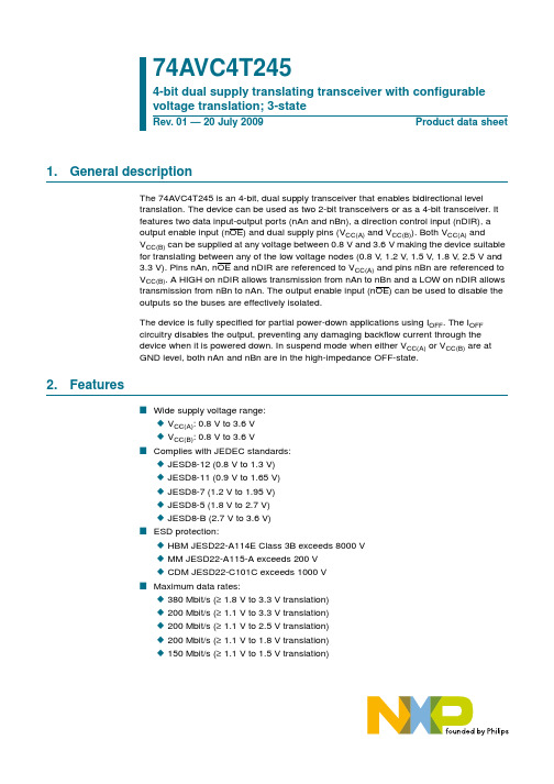
terminal 1 index area
1DIR 2 2DIR 3 1A1 4 1A2 5 2A1 6 2A2 7
GND(1)
15 1OE 14 2OE 13 1B1 12 1B2 11 2B1 10 2B2
GND 8 GND 9
001aak284
Transparent top view
(1) The die substrate is attached to this pad using conductive die attach material. It cannot be used as a supply pin or input.
2B2, 2B1 10, 11
1B2, 1B1 12, 13
2OE, 1OE 14, 15
VCC(B)
16
Description supply voltage A (nAn, nOE and nDIR inputs are referenced to VCC(A)) direction control data input or output data input or output ground (0 V) data input or output data input or output output enable input (active LOW) supply voltage B (nBn inputs are referenced to VCC(B))
Fig 5. Pin configuration SOT763-1 (DHVQFN16)
5.2 Pin description
Table 2. Pin description
Symbol
Pin
VCC(A)
SN74AVC16T245中文资料

元器件交易网元器件交易网元器件交易网IMPORTANT NOTICETexas Instruments Incorporated and its subsidiaries (TI) reserve the right to make corrections, modifications,enhancements, improvements, and other changes to its products and services at any time and to discontinueany product or service without notice. Customers should obtain the latest relevant information before placingorders and should verify that such information is current and complete. All products are sold subject to TI’s termsand conditions of sale supplied at the time of order acknowledgment.TI warrants performance of its hardware products to the specifications applicable at the time of sale inaccordance with TI’s standard warranty. T esting and other quality control techniques are used to the extent TIdeems necessary to support this warranty. Except where mandated by government requirements, testing of allparameters of each product is not necessarily performed.TI assumes no liability for applications assistance or customer product design. Customers are responsible fortheir products and applications using TI components. T o minimize the risks associated with customer productsand applications, customers should provide adequate design and operating safeguards.TI does not warrant or represent that any license, either express or implied, is granted under any TI patent right,copyright, mask work right, or other TI intellectual property right relating to any combination, machine, or processin which TI products or services are used. Information published by TI regarding third-party products or servicesdoes not constitute a license from TI to use such products or services or a warranty or endorsement thereof.Use of such information may require a license from a third party under the patents or other intellectual propertyof the third party, or a license from TI under the patents or other intellectual property of TI.Reproduction of information in TI data books or data sheets is permissible only if reproduction is withoutalteration and is accompanied by all associated warranties, conditions, limitations, and notices. Reproductionof this information with alteration is an unfair and deceptive business practice. TI is not responsible or liable forsuch altered documentation.Resale of TI products or services with statements different from or beyond the parameters stated by TI for thatproduct or service voids all express and any implied warranties for the associated TI product or service andis an unfair and deceptive business practice. TI is not responsible or liable for any such statements.Following are URLs where you can obtain information on other Texas Instruments products and applicationsolutions:Products ApplicationsAmplifiers Audio /audioData Converters Automotive /automotiveDSP Broadband /broadbandInterface Digital Control /digitalcontrolLogic Military /militaryPower Mgmt Optical Networking /opticalnetworkMicrocontrollers Security /securityTelephony /telephonyVideo & Imaging /videoWireless /wirelessMailing Address:Texas InstrumentsPost Office Box 655303 Dallas, Texas 75265Copyright 2004, Texas Instruments Incorporated。
SN74HCT245NSR中文资料

PACKAGING INFORMATIONOrderable Device Status(1)PackageType PackageDrawingPins PackageQtyEco Plan(2)Lead/Ball Finish MSL Peak Temp(3)5962-8550601VRA ACTIVE CDIP J201None Call TI Level-NC-NC-NC 5962-8550601VSA ACTIVE CFP W201None Call TI Level-NC-NC-NC 85506012A ACTIVE LCCC FK201None Call TI Level-NC-NC-NC 8550601RA ACTIVE CDIP J201None Call TI Level-NC-NC-NC JM38510/65553BRA ACTIVE CDIP J201None Call TI Level-NC-NC-NC JM38510/65553BSA ACTIVE CFP W201None Call TI Level-NC-NC-NC SN54HCT245J ACTIVE CDIP J201None Call TI Level-NC-NC-NC SN74HCT245DBLE OBSOLETE SSOP DB20None Call TI Call TISN74HCT245DBR ACTIVE SSOP DB202000Pb-Free(RoHS)CU NIPDAU Level-2-260C-1YEAR/Level-1-235C-UNLIMSN74HCT245DW ACTIVE SOIC DW2025Pb-Free(RoHS)CU NIPDAU Level-2-250C-1YEAR/Level-1-235C-UNLIMSN74HCT245DWR ACTIVE SOIC DW202000Pb-Free(RoHS)CU NIPDAU Level-2-250C-1YEAR/Level-1-235C-UNLIMSN74HCT245N ACTIVE PDIP N2020Pb-Free(RoHS)CU NIPDAU Level-NC-NC-NC SN74HCT245N3OBSOLETE PDIP N20None Call TI Call TISN74HCT245NSR ACTIVE SO NS202000Pb-Free(RoHS)CU NIPDAU Level-2-260C-1YEAR/Level-1-235C-UNLIMSN74HCT245PW ACTIVE TSSOP PW2070Pb-Free(RoHS)CU NIPDAU Level-1-250C-UNLIMSN74HCT245PWLE OBSOLETE TSSOP PW20None Call TI Call TISN74HCT245PWR ACTIVE TSSOP PW202000Pb-Free(RoHS)CU NIPDAU Level-1-250C-UNLIMSN74HCT245PWT ACTIVE TSSOP PW20250Pb-Free(RoHS)CU NIPDAU Level-1-250C-UNLIM SNJ54HCT245FK ACTIVE LCCC FK201None Call TI Level-NC-NC-NC SNJ54HCT245J ACTIVE CDIP J201None Call TI Level-NC-NC-NC SNJ54HCT245W ACTIVE CFP W201None Call TI Level-NC-NC-NC (1)The marketing status values are defined as follows:ACTIVE:Product device recommended for new designs.LIFEBUY:TI has announced that the device will be discontinued,and a lifetime-buy period is in effect.NRND:Not recommended for new designs.Device is in production to support existing customers,but TI does not recommend using this part in a new design.PREVIEW:Device has been announced but is not in production.Samples may or may not be available.OBSOLETE:TI has discontinued the production of the device.(2)Eco Plan-May not be currently available-please check /productcontent for the latest availability information and additional product content details.None:Not yet available Lead(Pb-Free).Pb-Free(RoHS):TI's terms"Lead-Free"or"Pb-Free"mean semiconductor products that are compatible with the current RoHS requirements for all6substances,including the requirement that lead not exceed0.1%by weight in homogeneous materials.Where designed to be soldered at high temperatures,TI Pb-Free products are suitable for use in specified lead-free processes.Green(RoHS&no Sb/Br):TI defines"Green"to mean"Pb-Free"and in addition,uses package materials that do not contain halogens, including bromine(Br)or antimony(Sb)above0.1%of total product weight.(3)MSL,Peak Temp.--The Moisture Sensitivity Level rating according to the JEDECindustry standard classifications,and peak solder temperature.Important Information and Disclaimer:The information provided on this page represents TI's knowledge and belief as of the date that it is provided.TI bases its knowledge and belief on information provided by third parties,and makes no representation or warranty as to the accuracy of such information.Efforts are underway to better integrate information from third parties.TI has taken and continues to take reasonable steps to provide representative and accurate information but may not have conducted destructive testing or chemical analysis on incoming materials and chemicals.TI and TI suppliers consider certain information to be proprietary,and thus CAS numbers and other limited information may not be available for release.In no event shall TI's liability arising out of such information exceed the total purchase price of the TI part(s)at issue in this document sold by TI to Customer on an annual basis.元器件交易网IMPORTANT NOTICETexas Instruments Incorporated and its subsidiaries (TI) reserve the right to make corrections, modifications,enhancements, improvements, and other changes to its products and services at any time and to discontinueany product or service without notice. Customers should obtain the latest relevant information before placingorders and should verify that such information is current and complete. All products are sold subject to TI’s termsand conditions of sale supplied at the time of order acknowledgment.TI warrants performance of its hardware products to the specifications applicable at the time of sale inaccordance with TI’s standard warranty. T esting and other quality control techniques are used to the extent TIdeems necessary to support this warranty. Except where mandated by government requirements, testing of allparameters of each product is not necessarily performed.TI assumes no liability for applications assistance or customer product design. Customers are responsible fortheir products and applications using TI components. T o minimize the risks associated with customer productsand applications, customers should provide adequate design and operating safeguards.TI does not warrant or represent that any license, either express or implied, is granted under any TI patent right,copyright, mask work right, or other TI intellectual property right relating to any combination, machine, or processin which TI products or services are used. Information published by TI regarding third-party products or servicesdoes not constitute a license from TI to use such products or services or a warranty or endorsement thereof.Use of such information may require a license from a third party under the patents or other intellectual propertyof the third party, or a license from TI under the patents or other intellectual property of TI.Reproduction of information in TI data books or data sheets is permissible only if reproduction is withoutalteration and is accompanied by all associated warranties, conditions, limitations, and notices. Reproductionof this information with alteration is an unfair and deceptive business practice. TI is not responsible or liable forsuch altered documentation.Resale of TI products or services with statements different from or beyond the parameters stated by TI for thatproduct or service voids all express and any implied warranties for the associated TI product or service andis an unfair and deceptive business practice. TI is not responsible or liable for any such statements.Following are URLs where you can obtain information on other Texas Instruments products and applicationsolutions:Products ApplicationsAmplifiers Audio /audioData Converters Automotive /automotiveDSP Broadband /broadbandInterface Digital Control /digitalcontrolLogic Military /militaryPower Mgmt Optical Networking /opticalnetworkMicrocontrollers Security /securityTelephony /telephonyVideo & Imaging /videoWireless /wirelessMailing Address:Texas InstrumentsPost Office Box 655303 Dallas, Texas 75265Copyright 2005, Texas Instruments Incorporated。
HD74ACT245中文资料
HD74AC245/HD74ACT245 Octal Bidirectional Transceiver with 3-State Input/OutputDescriptionThe HD74AC245/HD74ACT245 contains eight non-inverting bidirectional buffers with 3-state outputs and is intended for bus-oriented applications. Current sinking capability is 24 mA at both the A and B ports. The Transmit/Receive (T/R) input determines the direction of data flow through the bidirectional transceiver. Transmit (active-High) enables data from A ports to B ports; Receive (active-Low) enables data from B ports to A ports. The Output Enable input, when High, disables, both A and B ports by placing them in a High Z condition.Features• Noninverting Buffers• Bidirectional Data Path• A and B Outputs Source/Sink 24 mA• HD74ACT245 has TTL-Compatible InputsPin NamesOE Output Enable InputT/R Transmit/Receive InputA0 to A7Side A 3-State Inputs or 3-State OutputsB0 to B7Side B 3-State Inputs or 3-State OutputsHD74AC245/HD74ACT245Pin ArrangementTruth TablesInputsOE T/R OutputsL L Bus B Data to Bus A L H Bus A Data to Bus B H X High Z StateH:High Voltage LevelL:Low Voltage LevelX:Immaterial2HD74AC245/HD74ACT2453DC Characteristics (unless otherwise specified)ItemSymbol Max Unit ConditionMaximum quiescent supply current I CC 80µA V IN = V CC or ground, V CC = 5.5 V,Ta = Worst caseMaximum quiescent supply current I CC 8.0µA V IN = V CC or ground, V CC = 5.5 V,Ta = 25°CMaximum additional I CC /input (HD74ACT245)I CCT1.5mAV IN = V CC – 2.1 V, V CC = 5.5 V,Ta = Worst caseAC Characteristics: HD74AC245Ta = +25°C C L = 50 pFTa = –40°C to +85°C C L = 50 pF ItemSymbol V CC (V)*1Min Typ Max Min Max Unit Propagation delay t PLH3.3 1.0 5.08.5 1.09.0nsData to output 5.0 1.0 3.5 6.5 1.07.0Propagation delay t PHL 3.3 1.0 5.08.5 1.09.0ns Data to output 5.0 1.0 3.5 6.0 1.07.0Output enable time t PZH 3.3 1.07.011.5 1.012.5ns 5.0 1.0 5.08.5 1.09.0Output enable time t PZL 3.3 1.07.512.0 1.013.5ns 5.0 1.0 5.59.0 1.09.5Output disable time t PHZ 3.3 1.0 6.512.0 1.012.5ns 5.0 1.0 5.59.0 1.010.0Output disable time t PLZ 3.3 1.07.011.5 1.013.0ns 5.01.05.59.01.010.0Note:1.Voltage Range 3.3 is 3.3 V ± 0.3 VVoltage Range 5.0 is 5.0 V ± 0.5 VHD74AC245/HD74ACT2454AC Characteristics: HD74ACT245Ta = +25°C C L = 50 pFTa = –40°C to +85°C C L = 50 pF ItemSymbol V CC (V)*1Min Typ Max Min Max Unit Propagation delay Data to output t PLH 5.0 1.0 4.07.5 1.08.0ns Propagation delay Data to output t PHL 5.0 1.0 4.08.0 1.09.0ns Output enable time t PZH 5.0 1.0 5.010.0 1.011.0ns Output enable time t PZL 5.0 1.0 5.510.0 1.012.0ns Output disable time t PHZ 5.0 1.0 5.510.0 1.011.0ns Output disable time t PLZ5.01.05.010.01.011.0nsNote:1.Voltage Range 5.0 is 5.0 V ± 0.5 VCapacitanceItemSymbol Typ Unit Condition Input capacitance C IN 4.5pF V CC = 5.5 V Input/output capacitance C I/O 15.0pF V CC = 5.5 V Power dissipation capacitanceC PD45.0pFV CC = 5.0 VHitachi Code JEDEC EIAJWeight (reference value)DP-20N —Conforms 1.26 gUnit: mm元器件交易网Hitachi Code JEDEC EIAJWeight (reference value)TTP-20DA ——0.07 gUnit: mm*Dimension including the plating thicknessBase material dimension元器件交易网Cautions1.Hitachi neither warrants nor grants licenses of any rights of Hitachi’s or any third party’s patent,copyright, trademark, or other intellectual property rights for information contained in this document.Hitachi bears no responsibility for problems that may arise with third party’s rights, includingintellectual property rights, in connection with use of the information contained in this document.2.Products and product specifications may be subject to change without notice. Confirm that you have received the latest product standards or specifications before final design, purchase or use.3.Hitachi makes every attempt to ensure that its products are of high quality and reliability. However,contact Hitachi’s sales office before using the product in an application that demands especially high quality and reliability or where its failure or malfunction may directly threaten human life or cause risk of bodily injury, such as aerospace, aeronautics, nuclear power, combustion control, transportation,traffic, safety equipment or medical equipment for life support.4.Design your application so that the product is used within the ranges guaranteed by Hitachi particularly for maximum rating, operating supply voltage range, heat radiation characteristics, installationconditions and other characteristics. Hitachi bears no responsibility for failure or damage when used beyond the guaranteed ranges. Even within the guaranteed ranges, consider normally foreseeable failure rates or failure modes in semiconductor devices and employ systemic measures such as fail-safes, so that the equipment incorporating Hitachi product does not cause bodily injury, fire or other consequential damage due to operation of the Hitachi product.5.This product is not designed to be radiation resistant.6.No one is permitted to reproduce or duplicate, in any form, the whole or part of this document without written approval from Hitachi.7.Contact Hitachi’s sales office for any questions regarding this document or Hitachi semiconductor products.Hitachi, Ltd.Semiconductor & Integrated Circuits.Nippon Bldg., 2-6-2, Ohte-machi, Chiyoda-ku, Tokyo 100-0004, Japan Tel: Tokyo (03) 3270-2111 Fax: (03) 3270-5109Copyright ' Hitachi, Ltd., 1999. All rights reserved. Printed in Japan.Hitachi Asia Pte. Ltd.16 Collyer Quay #20-00Hitachi TowerSingapore 049318Tel: 535-2100Fax: 535-1533URLNorthAmerica : http:/Europe : /hel/ecg Asia (Singapore): .sg/grp3/sicd/index.htm Asia (Taiwan): /E/Product/SICD_Frame.htm Asia (HongKong): /eng/bo/grp3/index.htm Japan : http://www.hitachi.co.jp/Sicd/indx.htmHitachi Asia Ltd.Taipei Branch Office3F, Hung Kuo Building. No.167, Tun-Hwa North Road, Taipei (105)Tel: <886> (2) 2718-3666Fax: <886> (2) 2718-8180Hitachi Asia (Hong Kong) Ltd.Group III (Electronic Components)7/F., North Tower, World Finance Centre,Harbour City, Canton Road, Tsim Sha Tsui,Kowloon, Hong Kong Tel: <852> (2) 735 9218Fax: <852> (2) 730 0281 Telex: 40815 HITEC HXHitachi Europe Ltd.Electronic Components Group.Whitebrook ParkLower Cookham Road MaidenheadBerkshire SL6 8YA, United Kingdom Tel: <44> (1628) 585000Fax: <44> (1628) 778322Hitachi Europe GmbHElectronic components Group Dornacher Stra§e 3D-85622 Feldkirchen, Munich GermanyTel: <49> (89) 9 9180-0Fax: <49> (89) 9 29 30 00Hitachi Semiconductor (America) Inc.179 East Tasman Drive,San Jose,CA 95134 Tel: <1> (408) 433-1990Fax: <1>(408) 433-0223For further information write to:。
74VHC245中文资料
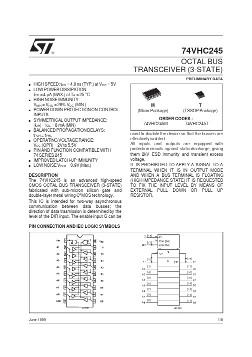
74VHC245OCTAL BUS TRANSCEIVER(3-STATE)PRELIMINARY DATAJune1999ORDER CODES:74VHC245M74VHC245T M(Micro Package)s HIGH SPEED:t PD=4.0ns(TYP.)at V CC=5V s LOW POWER DISSIPATION:I CC=4µA(MAX.)at T A=25o Cs HIGH NOISE IMMUNITY:V NIH=V NIL=28%V CC(MIN.)s POWER DOWN PROTECTION ON CONTROL INPUTSs SYMMETRICAL OUTPUT IMPEDANCE: |I OH|=I OL=8mA(MIN)s BALANCED PROPAGATION DELAYS: t PLH≅t PHLs OPERATING VOLTAGERANGE:V CC(OPR)=2V to5.5Vs PIN AND FUNCTION COMPATIBLE WITH 74SERIES245s IMPROVED LATCH-UP IMMUNITYs LOW NOISEV OLP=0.9V(Max.) DESCRIPTIONThe74VHC245is an advanced high-speed CMOS OCTAL BUS TRANSCEIVER(3-STATE) fabricated with sub-micron silicon gate and double-layer metal wiring C2MOS technology. This IC is intended for two-way asynchronous communication between data busses;the direction of data trasmission is determined by the level of the DIR input.The enable input G can beT(TSSOP Package) used to disable the device so that the busses are effectively isolated.All inputs and outputs are equipped with protection circuits against static discharge,giving them2kV ESD immunity and transient excess voltage.IT IS PROHIBITED TO APPLY A SIGNAL TO A TERMINAL WHEN IT IS IN OUTPUT MODE AND WHEN A BUS TERMINAL IS FLOATING (HIGH IMPEDANCE STATE)IT IS REQUESTED TO FIX THE INPUT LEVEL BY MEANS OF EXTERNAL PULL DOWN OR PULL UP RESISTOR.PIN CONNECTION AND IEC LOGIC SYMBOLS®1/8PIN DESCRIPTIONPIN No SYMBOL NAME AND FUNCTION1DIR Directional Control2,3,4,5,6,7,8,9A1to A8Data Inputs/Outputs18,17,16,15,14,13,12,11B1to B8Data Inputs/Outputs19G Output Enable Input10GND Ground(0V)20V CC Positive Supply VoltageTRUTH TABLEINPUT FUNCTION OUTPUTG DIR A BUS B BUSL L OUTPUT INPUT A=BL H INPUT OUTPUT B=AH X Z Z ZX:”H”or”L”Z:High impe danceINPUT EQUIVALENT CIRCUITABSOLUTE MAXIMUM RATINGSSymbol Parameter Value Unit V CC Supply Voltage-0.5to+7.0V V I DC Input Voltage(DIR,G)-0.5to+7.0V V I/O Bus I/O Voltage-0.5to V CC+0.5V V O DC Output Voltage-0.5to V CC+0.5VI IK DC Input Diode Current-20mAI OK DC Output Diode Current±20mAI O DC Output Current±25mA I CC or I GND DC V CC or Ground Current±75mAT stg Storage Temperature-65to+150o C T L Lead Temperature(10sec)300o C Absolute Maximum Ratingsarethose values beyond which dam age to the device may occur.Functional operation un der these condition is not implied.RECOMMENDED OPERATING CONDITIONSSymbol Parameter Value Unit V CC Supply Voltage 2.0to5.5V V I Input Voltage(DIR,G)0to5.5V V I/O Bus I/O Voltage0to V CC V V O Output Voltage0to V CC V T op Operating Temperature-40to+85o Cdt/dv Input Rise and Fall Time(see note1)(V CC=3.3±0.3V)(V CC=5.0±0.5V)0to1000to20ns/Vns/V1)V IN from30%to70%of V CC 74VHC2452/8DC SPECIFICATIONSSymbolParameterTest Conditions ValueUnitV CC (V)T A =25oC -40to 85oC Min.Typ.Max.Min.Max.V IH High Level Input Voltage 2.0 1.5 1.5V 3.0to 5.50.7V CC0.7V CCV IL Low Level Input Voltage2.00.50.5V3.0to 5.50.3V CC0.3V CC V OHHigh Level Output Voltage2.0I O =-50µA 1.9 2.0 1.9V3.0I O =-50µA 2.9 3.0 2.94.5I O =-50µA 4.4 4.54.43.0I O =-4mA 2.58 2.484.5I O =-8mA 3.943.8V OLLow Level Output Voltage2.0I O =50µA 0.00.10.1V3.0I O =50µA 0.00.10.14.5I O =50µA 0.00.10.13.0I O =4mA 0.360.444.5I O =8mA 0.360.44I OZHigh Impedance Output Leakage Current5.5V I =V IH or V IL V O =V CC or GND ±0.25±2.5µAI I Input Leakage Current 0to 5.5V I =5.5V or GND ±0.1±1.0µA I CCQuiescent Supply Current5.5V I =V CC or GND440µAAC ELECTRICAL CHARACTERISTICS (Input t r =t f =3ns)SymbolParameterTest Condition ValueUnitV CC (V)C L (pF)T A =25oC-40to 85oC Min.Typ.Max.Min.Max.t PLH t PHL Propagation Delay Time3.3(*)15 5.88.4 1.010.0ns3.3(*)508.311.9 1.013.55.0(**)154.05.5 1.06.55.0(**)50 5.57.5 1.08.5t PLZ t PHZOutput Disable Time3.3(*)15R L =1K Ω8.513.2 1.015.5ns3.3(*)50R L =1K Ω11.016.7 1.019.05.0(**)15R L =1K Ω 5.88.5 1.010.05.0(**)50R L =1K Ω7.310.6 1.012.0t PZL t PZH Output Enable Time 3.3(*)50R L =1K Ω11.515.8 1.018.0ns 5.0(**)50R L =1K Ω7.09.7 1.011.0t OSLH t OSHLOutput to Output Skew Time (note 1)3.3(*)50 1.5 1.5ns5.0(**)501.01.0(*)Voltag e range is 3.3V ±0.3V (**)Voltage range is 5V ±0.5VNote 1:Parameter guaranteed bydesign.t soLH =|t pLHm -t pLHn |,t soHL =|t pHLm -t pHLn |74VHC2453/8CAPACITIVE CHARACTERISTICSSymbolParameterTest ConditionsValueUnitT A =25oC -40to 85oC Min.Typ.Max.Min.Max.C IN Input Capacitance 41010pF C I/O Bus Input Capacitance 8pF C PDPower Dissipation Capacitance (note 1)21pF1)C PD isdefined as the value of the IC’sinternal equiva lent capacitance which is calculated fromthe operating current consumption without load.(Referto Test Circuit).Average operting curren t can be obtained bythe followingequa tion.I CC (opr)=C PD •V CC •f IN +I CC /8(per circuit)TEST CIRCUITTESTSWITCH t PLH ,t PHL Open t PZL ,t PLZ V CC t PZH ,t PHZGNDC L =15/50pF or equ ivalent (includes jigand probe capacitance)R L =R 1=1K ΩorequivalentR T =Z OU T of pulse generator (typ ically 50Ω)DYNAMIC SWITCHING CHARACTERISTICSSymbolParameterTest Conditions ValueUnitV CC (V)T A =25oC -40to 85oC Min.Typ.Max.Min.Max.V OLP Dynamic Low Voltage Quiet Output (note 1,2) 5.0C L =50pF0.60.9VV OLV -0.9-0.6V IHD Dynamic High Voltage Input (note 1,3) 5.0 3.5V ILDDynamic Low Voltage Input (note 1,3)5.01.51)Worst case package.2)Max num ber of outputs defined as (n).Data inputs aredriven 0V to 5.0V,(n -1)outputs switching and one out put at GND.3)Max num ber of data inputs (n)switching.(n-1)switching 0V to5.0V.Inputs under test switching:5.0V to threshold (V ILD ),0V to threshold (V IHD ),f=1MHz.74VHC2454/874VHC245 WAVEFORM1:PROPAGATION DELAYS(f=1MHz;50%duty cycle)WAVEFORM2:OUTPUT ENABLE AND DISABLE TIME(f=1MHz;50%duty cycle)5/8DIM.mm inch MIN.TYP.MAX.MIN.TYP.MAX.A 2.650.104a10.100.200.0040.007a2 2.450.096b 0.350.490.0130.019b10.230.320.0090.012C 0.500.020c145(typ.)D 12.6013.000.4960.512E 10.0010.650.3930.419e 1.270.050e311.430.450F 7.407.600.2910.299L 0.50 1.270.190.050M 0.750.029S8(max.)P013LSO-20MECHANICAL DATA74VHC2456/8DIM.mminch MIN.TYP.MAX.MIN.TYP.MAX.A 1.10.433A10.050.100.150.0020.0040.006A20.850.90.950.3350.3540.374b 0.190.300.00750.0118c 0.090.20.00350.0079D 6.4 6.5 6.60.2520.2560.260E 6.25 6.4 6.50.2460.2520.256E1 4.34.4 4.480.1690.1730.176e 0.65BSC0.0256BSCK 0o 4o 8o 0o 4o 8o L0.500.600.700.0200.0240.028cEbA2AE1D1PIN 1IDENTIFICATIONA1LK eTSSOP20MECHANICAL DATA74VHC2457/874VHC245Information furnished is believed to be accurate and reliable.However,STMicroelectronics assumes no responsibility for the consequence s of use of such information nor for any infringement of patents or other rights of third parties which may result from its use.No license is granted by implication or otherwise under any patent or patent rights of STMicroelectronics.Specification mentioned in this publication are subject to change without notice.This publication supersedes and replaces all information previously supplied.STMicroelectronics products are not authorized for use as critical components in life support devices or systems without express written approval of STMicroelectronics.The ST logo is a trademark of STMicroelectronics©1999STMicroelectronics–Printed in Italy–All Rights ReservedSTMicroelectronics GROUP OF COMPANIESAustralia-Brazil-Canada-China-France-Germany-Italy-Japan-Korea-Malaysia-Malta-Mexico-Morocco-The Netherlands-Singapore-Spain-Sweden-Switzerland-Taiwan-Thailand-United Kingdom-U.S.A..8/8。
- 1、下载文档前请自行甄别文档内容的完整性,平台不提供额外的编辑、内容补充、找答案等附加服务。
- 2、"仅部分预览"的文档,不可在线预览部分如存在完整性等问题,可反馈申请退款(可完整预览的文档不适用该条件!)。
- 3、如文档侵犯您的权益,请联系客服反馈,我们会尽快为您处理(人工客服工作时间:9:00-18:30)。
元器件交易网
元器件交易网
元器件交易网
IMPORTANT NOTICE
Texas Instruments Incorporated and its subsidiaries (TI) reserve the right to make corrections, modifications,
enhancements, improvements, and other changes to its products and services at any time and to discontinue
any product or service without notice. Customers should obtain the latest relevant information before placing
orders and should verify that such information is current and complete. All products are sold subject to TI’s terms
and conditions of sale supplied at the time of order acknowledgment.
TI warrants performance of its hardware products to the specifications applicable at the time of sale in
accordance with TI’s standard warranty. T esting and other quality control techniques are used to the extent TI
deems necessary to support this warranty. Except where mandated by government requirements, testing of all
parameters of each product is not necessarily performed.
TI assumes no liability for applications assistance or customer product design. Customers are responsible for
their products and applications using TI components. T o minimize the risks associated with customer products
and applications, customers should provide adequate design and operating safeguards.
TI does not warrant or represent that any license, either express or implied, is granted under any TI patent right,
copyright, mask work right, or other TI intellectual property right relating to any combination, machine, or process
in which TI products or services are used. Information published by TI regarding third-party products or services
does not constitute a license from TI to use such products or services or a warranty or endorsement thereof.
Use of such information may require a license from a third party under the patents or other intellectual property
of the third party, or a license from TI under the patents or other intellectual property of TI.
Reproduction of information in TI data books or data sheets is permissible only if reproduction is without
alteration and is accompanied by all associated warranties, conditions, limitations, and notices. Reproduction
of this information with alteration is an unfair and deceptive business practice. TI is not responsible or liable for
such altered documentation.
Resale of TI products or services with statements different from or beyond the parameters stated by TI for that
product or service voids all express and any implied warranties for the associated TI product or service and
is an unfair and deceptive business practice. TI is not responsible or liable for any such statements.
Following are URLs where you can obtain information on other Texas Instruments products and application
solutions:
Products Applications
Amplifiers Audio /audio
Data Converters Automotive /automotive
DSP Broadband /broadband
Interface Digital Control /digitalcontrol
Logic Military /military
Power Mgmt Optical Networking /opticalnetwork
Microcontrollers Security /security
Telephony /telephony
Video & Imaging /video
Wireless /wireless
Mailing Address:Texas Instruments
Post Office Box 655303 Dallas, Texas 75265
Copyright 2004, Texas Instruments Incorporated。
