V23818-K305-B57中文资料
莫克8口无管理以太网开关产品说明书
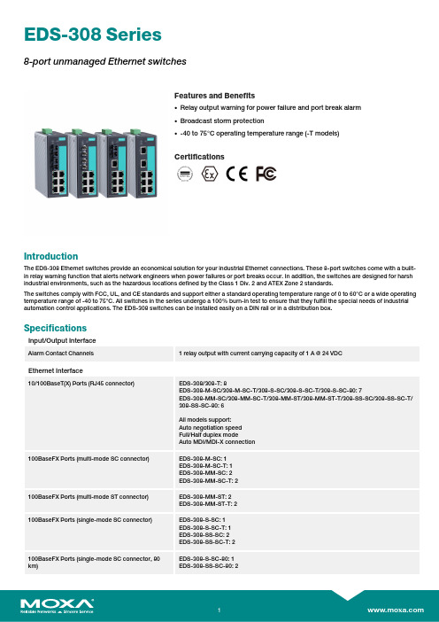
EDS-308Series8-port unmanaged Ethernet switchesFeatures and Benefits•Relay output warning for power failure and port break alarm •Broadcast storm protection•-40to 75°C operating temperature range (-T models)CertificationsIntroductionThe EDS-308Ethernet switches provide an economical solution for your industrial Ethernet connections.These 8-port switches come with a built-in relay warning function that alerts network engineers when power failures or port breaks occur.In addition,the switches are designed for harsh industrial environments,such as the hazardous locations defined by the Class 1Div.2and ATEX Zone 2standards.The switches comply with FCC,UL,and CE standards and support either a standard operating temperature range of 0to 60°C or a wide operating temperature range of -40to 75°C.All switches in the series undergo a 100%burn-in test to ensure that they fulfill the special needs of industrial automation control applications.The EDS-308switches can be installed easily on a DIN rail or in a distribution box.SpecificationsInput/Output InterfaceAlarm Contact Channels1relay output with current carrying capacity of 1A @24VDCEthernet Interface10/100BaseT(X)Ports (RJ45connector)EDS-308/308-T:8EDS-308-M-SC/308-M-SC-T/308-S-SC/308-S-SC-T/308-S-SC-80:7EDS-308-MM-SC/308-MM-SC-T/308-MM-ST/308-MM-ST-T/308-SS-SC/308-SS-SC-T/308-SS-SC-80:6All models support:Auto negotiation speed Full/Half duplex modeAuto MDI/MDI-X connection100BaseFX Ports (multi-mode SC connector)EDS-308-M-SC:1EDS-308-M-SC-T:1EDS-308-MM-SC:2EDS-308-MM-SC-T:2100BaseFX Ports (multi-mode ST connector)EDS-308-MM-ST:2EDS-308-MM-ST-T:2100BaseFX Ports (single-mode SC connector)EDS-308-S-SC:1EDS-308-S-SC-T:1EDS-308-SS-SC:2EDS-308-SS-SC-T:2100BaseFX Ports (single-mode SC connector,80km)EDS-308-S-SC-80:1EDS-308-SS-SC-80:2Standards IEEE802.3for10BaseTIEEE802.3u for100BaseT(X)and100BaseFXIEEE802.3x for flow controlOptical Fiber800Typical Distance4km5km40km80kmWavelen-gthTypical(nm)130013101550TX Range(nm)1260to13601280to13401530to1570 RX Range(nm)1100to16001100to16001100to1600Optical PowerTX Range(dBm)-10to-200to-50to-5 RX Range(dBm)-3to-32-3to-34-3to-34 Link Budget(dB)122929 Dispersion Penalty(dB)311Note:When connecting a single-mode fiber transceiver,we recommend using anattenuator to prevent damage caused by excessive optical power.Note:Compute the“typical distance”of a specific fiber transceiver as follows:Linkbudget(dB)>dispersion penalty(dB)+total link loss(dB).DIP Switch ConfigurationEthernet Interface Port break alarmSwitch PropertiesMAC Table Size2kbitsPacket Buffer Size768KProcessing Type Store and ForwardPower ParametersInput Current EDS-308/308-T:0.07A@24VDCEDS-308-M-SC/S-SC Series,308-S-SC-80:0.12A@24VDCEDS-308-MM-SC/MM-ST/SS-SC Series,308-SS-SC-80:0.15A@24VDC Connection1removable6-contact terminal block(s)Operating Voltage9.6to60VDCInput Voltage Redundant dual inputs,12/24/48VDCReverse Polarity Protection SupportedOverload Current Protection SupportedPhysical CharacteristicsHousing MetalIP Rating IP30Dimensions53.6x135x105mm(2.11x5.31x4.13in)Weight790g(1.75lb)Installation DIN-rail mounting,Wall mounting(with optional kit) Environmental LimitsOperating Temperature Standard Models:-10to60°C(14to140°F)Wide Temp.Models:-40to75°C(-40to167°F) Storage Temperature(package included)-40to85°C(-40to185°F)Ambient Relative Humidity5to95%(non-condensing)Standards and CertificationsHazardous Locations ATEX,Class I Division2EMI CISPR32,FCC Part15B Class AMaritime DNV-GLEMC EN55032/24Vibration IEC60068-2-6EMS IEC61000-4-2ESD:Contact:6kV;Air:8kVIEC61000-4-3RS:80MHz to1MHz:20V/mIEC61000-4-4EFT:Power:2kV;Signal:1kVIEC61000-4-5Surge:Power:2kV;Signal:2kVIEC61000-4-6CS:10VIEC61000-4-8PFMFSafety UL508,UL60950-1,CSA C22.2No.60950-1 Shock IEC60068-2-27Freefall IEC60068-2-32MTBFTime255,528hrsStandards MIL-HDBK-217FWarrantyWarranty Period5yearsDetails See /warrantyPackage ContentsDevice1x EDS-308Series switchInstallation Kit1x cap,plastic,for SC fiber port2x cap,plastic,for SC fiber port(-SC models)2x cap,plastic,for ST fiber port(-ST models) Documentation1x quick installation guide1x warranty cardDimensionsOrdering InformationModel Name 10/100BaseT(X)PortsRJ45Connector100BaseFX PortsMulti-Mode,SCConnector100BaseFX PortsMulti-Mode,STConnector100BaseFX PortsSingle-Mode,SCConnectorOperating Temp.EDS-3088–––0to60°CEDS-308-T8–––-40to75°C EDS-308-M-SC71––0to60°CEDS-308-M-SC-T71––-40to75°C EDS-308-MM-SC62––0to60°CEDS-308-MM-SC-T62––-40to75°C EDS-308-MM-ST6–2–0to60°CEDS-308-MM-ST-T6–2–-40to75°C EDS-308-S-SC7––10to60°CEDS-308-S-SC-T7––1-40to75°C EDS-308-SS-SC6––20to60°CEDS-308-SS-SC-T6––2-40to75°C EDS-308-S-SC-807––10to60°CEDS-308-SS-SC-806––20to60°C Accessories(sold separately)Power SuppliesDR-120-24120W/2.5A DIN-rail24VDC power supply with universal88to132VAC or176to264VAC input byswitch,or248to370VDC input,-10to60°C operating temperatureDR-452445W/2A DIN-rail24VDC power supply with universal85to264VAC or120to370VDC input,-10to50°C operating temperatureDR-75-2475W/3.2A DIN-rail24VDC power supply with universal85to264VAC or120to370VDC input,-10to60°C operating temperatureMDR-40-24DIN-rail24VDC power supply with40W/1.7A,85to264VAC,or120to370VDC input,-20to70°Coperating temperatureMDR-60-24DIN-rail24VDC power supply with60W/2.5A,85to264VAC,or120to370VDC input,-20to70°Coperating temperatureWall-Mounting KitsWK-46Wall-mounting kit,2plates,8screws,46.5x66.8x1mmRack-Mounting KitsRK-4U19-inch rack-mounting kit©Moxa Inc.All rights reserved.Updated Jan30,2019.This document and any portion thereof may not be reproduced or used in any manner whatsoever without the express written permission of Moxa Inc.Product specifications subject to change without notice.Visit our website for the most up-to-date product information.。
华为光模块属性
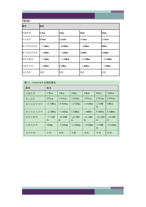
交换机常用模块:
倚窗远眺,目光目光尽处必有一座山,那影影绰绰的黛绿色的影,是春天的颜色。
周遭流岚升腾,没露出那真实的面孔。
面对那流转的薄雾,我会幻想,那里有一个世外桃源。
在天阶夜色凉如水的夏夜,我会静静地,静静地,等待一场流星雨的来临…
许下一个愿望,不乞求去实现,至少,曾经,有那么一刻,我那还未枯萎的,青春的,诗意的心,在我最美的年华里,同星空做了一次灵魂的交流…
秋日里,阳光并不刺眼,天空是一碧如洗的蓝,点缀着飘逸的流云。
偶尔,一片飞舞的落叶,会飘到我的窗前。
斑驳的印迹里,携刻着深秋的颜色。
在一个落雪的晨,这纷纷扬扬的雪,飘落着一如千年前的洁白。
窗外,是未被污染的银白色世界。
我会去迎接,这人间的圣洁。
在这流转的岁月里,有着流转的四季,还有一颗流转的心,亘古不变的心。
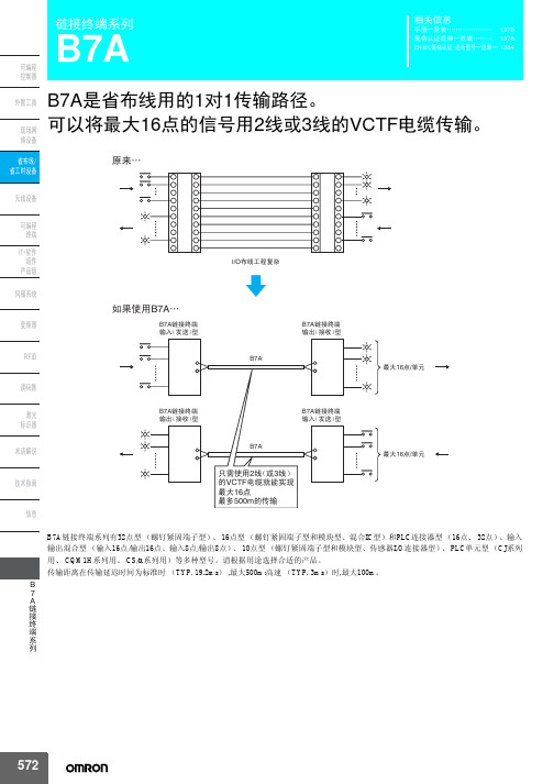
b7a
螺钉紧固端子
输入 (接收)
Ԏ᳡㋏㒳
模块
标准 (TYP. 19.2ms)
NPN对应输入 (不能连接2线性传
感器)
仅限- +-交互
标准 (TYP. 19.2ms)
TTL输入
--
型号 DRT1-B7AC
海外标准
U、 CU、 CE
型号
海外标准
B7A-T10S1 *1 B7A-T10S3 *1
U、C、 CE
B7A-T10M2
*2
--
型号
B7A-R6B11 B7A-R6B31 B7A-R6C11 B7A-R6C31 B7A-R6F11 B7A-R6F31 B7A-R6G11 B7A-R6G31 B7A-R6B16 B7A-R6B36 B7A-R6C16 B7A-R6C36 B7A-R6F16 B7A-R6F36 B7A-R6G16 B7A-R6G36 B7AS-R6B11
输出 32点
(16点×2端口)
输入
输入 64点 (16点×4端口)
输出
输出 64点 (16点×4端口)
传输延迟时间
错误时的输出处理 I/O单元占有CH
标准 (TYP. 19.2ms)
高速 (TYP. 3ms)
可切换
HOLD (仅限输入)
HOLD --
输入2CH 输出2CH
输入形态
+-端子结构
NPN对应输入
+-交互
输入形态 NPN对应输入 PNP对应输入 NPN对应输入 PNP对应输入
+-端子结构 仅限-
+-交互 +-交互
仅限- +-交互 +-交互
NPN对应输入
+-交互
TTL输入
--
NPN输入
铝电合成电容器说明书

本产品目录之规格如有变更恕不另行通知(CAT. 2018C1)137RZW 系列特长/用途‧105℃, 4,000 ~ 10,000小时寿命保证‧低等效串联电阻(ESR),适用交换式电源供应器(SPS) ‧制品尺寸较小并可承受大纹波电流 ‧符合RoHS 指令套管与标示颜色:黑色/金色规格表寸法图制品各项寸法单位:毫米φD 5 6.3 8 10 12.5 16 18 P 2.02.53.55.0 5.07.57.5 φd 0.50.60.8α L<20: 1.5, L ≧20: 2.0β0.5制品尺寸如为12.5×16、16×16、16×20、18×16、18×20、18×25适用下列制品尺寸图:引线型容许纹波电流:毫安/均方根值(mA/rms),100k赫兹(Hz), 105℃制品尺寸与容许纹波电流一览表阻抗值:欧姆(Ω)/最大值,100k赫兹(Hz), 20℃本产品目录之规格如有变更恕不另行通知(CAT. 2018C1)138容许纹波电流:毫安/均方根值(mA/rms),100k赫兹(Hz), 105℃制品尺寸与容许纹波电流一览表阻抗值:欧姆(Ω)/最大值,100k赫兹(Hz), 20℃产品编码说明RZW系列470微法拉± 20% 16V 长脚8φ×15L 无铅引线与PET套管RZW 471 M 1C BK - 0815系列额定静电容量额定静电容量容许误差值额定电压引线加工/包装型式胶盖型式制品尺寸制品引线与套管材质注:如需了解更详细之介绍,请参阅目录第13页”引线型产品编码说明”。
引线型本产品目录之规格如有变更恕不另行通知(CAT. 2018C1) 139。
A3058EU资料
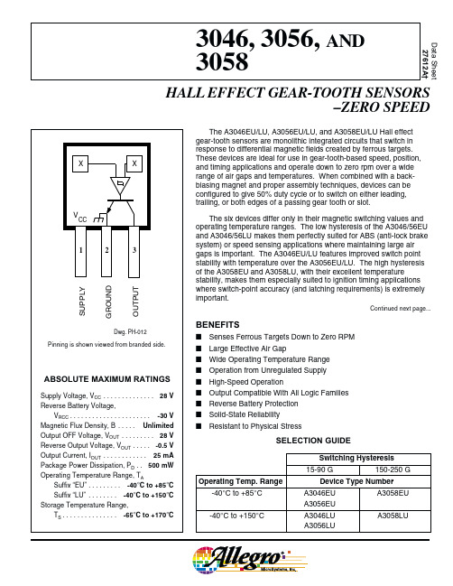
Switching Hysteresis 15-90 G150-250 G Operating Temp. RangeDevice Type Number-40°C to +85°C A3046EU A3058EU A3056EU -40°C to +150°CA3046LU A3058LUA3056LUHALL EFFECT GEAR-TOOTH SENSORS–ZERO SPEEDThe A3046EU/LU, A3056EU/LU, and A3058EU/LU Hall effect gear-tooth sensors are monolithic integrated circuits that switch in response to differential magnetic fields created by ferrous targets.These devices are ideal for use in gear-tooth-based speed, position,and timing applications and operate down to zero rpm over a wide range of air gaps and temperatures. When combined with a back-biasing magnet and proper assembly techniques, devices can be configured to give 50% duty cycle or to switch on either leading,trailing, or both edges of a passing gear tooth or slot.The six devices differ only in their magnetic switching values and operating temperature ranges. The low hysteresis of the A3046/56EU and A3046/56LU makes them perfectly suited for ABS (anti-lock brake system) or speed sensing applications where maintaining large air gaps is important. The A3046EU/LU features improved switch point stability with temperature over the A3056EU/LU. The high hysteresis of the A3058EU and A3058LU, with their excellent temperaturestability, makes them especially suited to ignition timing applications where switch-point accuracy (and latching requirements) is extremely important.Continued next page...BENEFITSI Senses Ferrous Targets Down to Zero RPM I Large Effective Air GapI Wide Operating Temperature Range I Operation from Unregulated Supply I High-Speed OperationI Output Compatible With All Logic Families I Reverse Battery Protection I Solid-State ReliabilityIResistant to Physical StressSELECTION GUIDEData Sheet27612A†3046, 3056, AND 30583046, 3056, AND 3058HALL EFFECTGEAR-TOOTH SENSORS–ZERO SPEED115 Northeast Cutoff, Box 15036Worcester, Massachusetts 01615-0036 (508) 853-5000All devices, when used with a back-biasing magnet, can be configured to turn ON or OFF with the leading or trailing edge of a gear tooth or slot. Changes in fields on the magnet face caused by a moving ferrous mass are sensed by two integrated Halltransducers and are differentially amplified by on-chip electronics. The on-chip temperature compensation and Schmitt trigger circuitry minimizes shifts in effective working air gaps and switch points over temperature making these devices ideal for use in ignition timing,anti-lock braking systems, and speed mea-surement systems in hostile automotive and industrial environments.Each Hall effect digital Integrated circuit includes two quadratic Hall effect sensing elements, a voltage regulator, temperature compensating circuitry, low-level amplifier,Schmitt trigger, and an open-collector output driver. The on-board regulator permits operation with supply voltages of 4.5 to 24volts. The output stage can switch up to 20mA at conservatively specified repetitionrates to 20 kHz and is compatible with bipolar and MOS logic circuits.Both magnetic characteristics are available in a choice of two operat-ing temperature ranges. Suffix EU devices have an operating range of -40°C to +85°C while suffix LU devices feature an operating range of -40°C to +150°C. All devices are packaged in a 3-pin plastic SIP.ELECTRICAL CHARACTERISTICS at V CC = 8 V, over operating temperature range.LimitsCharacteristic Symbol Test Conditions Min.Typ.Max.Units Supply Voltage V CC Operating4.5—24V Power-Up State—3058* only,Output is OFF—V CC = 0 4.5 V, B < B OP Output Saturation Voltage V OUT(SAT)I OUT = 20 mA, B > B OP —135400mV Output Leakage Current I OFF V CC = V OUT = 24 V, B < B RP —— 5.0µA Supply Current I CC V CC = 24 V, B < B RP —7.214mA Output Rise time t r R L = 820 Ω, C L = 20 pF —100—ns Output Fall timet fR L = 820 Ω, C L = 20 pF—100—nsCopyright © 1989, 1995 Allegro MicroSystems, Inc.3046, 3056, AND 3058HALL EFFECTGEAR-TOOTH SENSORS–ZERO SPEEDPart Numbers*304630563058Characteristic Test ConditionsMin.Typ.Max.Min.Typ.Max.Min.Typ. Max.Operate Point, B OPOutput Switches OFF to ON,——150——150——250Release Point, B RPOutput Switches ON to OFF,-150——-150——-250——Hysteresis, B hysB OP -B RP , T A = +25°C155090155090150200250Change in Trip Point,——±50——±75——±50∆B OP or ∆B RPMAGNETIC CHARACTERISTICS in gauss at V CC = 8 V.T A = +25°CT A = +25°C NOTES:1. Magnetic switch points are specified as thedifference in magnetic fields at the two Hall elements.2. As used here, negative flux densities are defined as less than zero (algebraic conven-tion).3. Typical values are at T A = +25°C.* Complete part number includes the prefix ‘A’ and a suffix to identify operating tempera-ture range and package style. See selection guide.Over operating temperature range,Ref. B OP or B RP at T A = +25°CTYPICAL OPERATING CHARACTERISTICS5S U P P L Y C U RR E N T I N m ASUPPLY VOLTAGE IN VOLTS Dwg. GH-031109876100S A T U R A TI O N V O L T A G E I N m VAMBIENT TEMPERATURE IN °CDwg. GH-0331801601401202005S U P P L Y C U R R E N T I N m AAMBIENT TEMPERATURE IN °CDwg. GH-032119876103046, 3056, AND 3058HALL EFFECTGEAR-TOOTH SENSORS–ZERO SPEED115 Northeast Cutoff, Box 15036Worcester, Massachusetts 01615-0036 (508) 853-5000O U T P U T V O L T A G E I N V O L T SDIFFERENTIAL FLUX DENSITY, B E1 – B E2Dwg. GH-034APPLICATIONS INFORMATIONA gear-tooth sensing system consists of the sensor IC, a back-biasing magnet, an optional pole piece, and a target (Figure 1). The system requirements are usually specified in terms of the effective working air gap between the package and the target (gear teeth), the number of switching events per rotation of the target, temperature and speed ranges, minimum pulse duration or duty cycle, and switch point accuracy. Careful choice of the sensor IC, magnet material andshape, target material and shape, and assembly techniques enables large working air gaps and high switch-point accuracy over the system operating temperature range.Naming Conventions. With a south pole in front of the branded surface of the sensor, a north pole behind the sensor, the field at the sensor is defined as positive. As used here, negative flux densities are defined as less than zero (algebraic convention), e.g., -100 G is less than -50 G.Magnet Biasing. In order to sense moving non-magnetized ferrous targets, these devices must be back-biased by mounting the unbranded side on a small permanent magnet. Either magnetic pole (north or south) can be used.The devices can also be used without a back-biasing magnet.In this configuration, the sensor can be used to detect a rotating ring magnet such as those found in brushless dc motors or in speed sensing applications. Here, the sensor detects the magnetic field gradient created by the magnetic poles.Figure 2TYPICAL TRANSFER CHARACTERISTICFigure 1TYPICAL GEAR-TOOTH SENSINGAPPLICATIONOPTIONAL POLE PIECESENSOR ICDwg. AH-0033046, 3056, AND 3058HALL EFFECTGEAR-TOOTH SENSORS–ZERO SPEEDSensor Operation. The A3046EU/LU,A3056EU/LU, and A3058EU/LU sensor ICs each contain two integrated Hall transducers (E1 and E2) that are used to sense a mag-netic field differential across the face of the IC (see S ENSOR L OCATION drawing). Referring to Figure 2, the trigger switches the output ON (output LOW) when B E1 – B E2 > B OP and switches the output OFF (output HIGH) when B E1 – B E2 < B RP . The difference between B OP and B RP is the hysteresis of the device.Figure 3 relates the output state of a back-biased sensor IC, with switching characteristics shown in Figure 2, to the target gear profile and position. Assume a north pole back-bias configuration (equivalent to south pole at the face of the device). The motion of the gear produces a phase-shifted field at E1 and E2 (Figure 3 (a)); internalconditioning circuitry subtracts the field at the two elements (Figure 3 (b)); and the Schmitt trigger at the output of the conditioning circuitry switches at the pre-determinedthresholds (B OP and B RP ). As shown (Figure 3 (c)), the IC output is LOW whenever sensor E1 sees a (ferrous) gear tooth and sensor E2faces air. The output is HIGH when sensor E1 sees air and sensor E2 sees the ferrous target.A gear-tooth sensor can be configured (see A SSEMBLY T ECHNIQUES ) to operate as a latch, a (positive) switch, or a negative switch. Note the change in duty cycle in each of the cases (Figure 4).A latch is a device where the operate point is greater than zero gauss and the release point is less than zero gauss. With the configuration shown in Figure 3, such a device will switch ON on the leading edge and OFF on the trailing edge of the target tooth.A (positive) switch is a device where both the operate and release points are greater than zero gauss (positive values).In the configuration shown in Figure 3, such a device will switch ONand then switch OFF on the leading or rising edge of the target tooth (Figure 4 (a)).A negative switch is a device where both the operate and release points are less than zero gauss (negative values). In the configuration shown in Figure 3, such a device will switch OFF and then switch ON on the trailing or falling edge of the target tooth (Figure 4 (b)).Speed sensors can use any of the three sensor configurations described. Timing sensors, however, must use a latch to guarantee dual-edge detection. Latches are most easily made using the A3058EU or A3058LU device types.3046, 3056, AND 3058HALL EFFECTGEAR-TOOTH SENSORS–ZERO SPEED115 Northeast Cutoff, Box 15036Worcester, Massachusetts 01615-0036 (508) 853-5000SYSTEM ISSUESOptimal performance of a gear-tooth sensing system strongly depends on four factors: the IC magnetic parameters, the magnet, the pole piece configuration, and the target.Sensor Specifications. Shown inFigure 5 are graphs of the differential field as a function of air gap. A 48-tooth, 2.5”(63.5 mm) diameter, uniform wheel similar to that used in ABS applications is used. The samarium cobalt magnet is 0.32” diameter by 0.20” long (8.13 x 5.08 mm). The maximum functioning air gap with this typical gear/magnet combination can be determined using the graphs and the specifications for the sensor IC.In this case, if an A3056EU/LU sensor with a B OP of +25 G and a B RP of -25 G is used, the maximum allowable air gap would be 0.110” (2.79 mm). If the switch points change +75 G with temperature (B OP = + 100G, B RP = +50 G), the maximum air gap will be approximately 0.077” (1.96 mm).All system issues should be translated back to such a profile to aid the prediction of system performance.Magnet Selection. These devices can be used with a wide variety of commercially available permanent magnets. The selection of the magnet depends on the operational and environmental requirements of the sensing system. For systems that require high accuracy and large working airgaps or an extended temperature range, the usual magnet material of choice is rare earth samarium cobalt (SmCo). This magnet material has a high energy product and can operate over an extended temperature range.For systems that require low-cost solutions for an extended temperature range, Alnico-8can be used. Due to its relatively low energy product, smaller operational airgaps can be expected. At this time, neodymium ironboron (NeFeB) is not a proven high-tempera-ture performer; at temperatures above+150°C it may irreversibly lose magnetic strength. Of these threemagnet materials, Alnico-8 is the least expensive by volume and SmCo is the most expensive.Either cylindrical- or cube-shaped magnets can be used, as long as the magnet pole face at least equals the facing surface(s) of the IC package and the pole piece. Choose the length of the magnet toobtain a high length-to-width ratio, up to 0.75:1 for rare earths, or 1.5:1for Alnico-8. Any added magnet length may incrementally improve the allowable maximum air gap.Magnets, in general, have a non-uniform magnetic surface profile.The flux across the face of a magnet can vary by as much as 5% of the average field over a 0.10” (2.5 mm) region. If a Hall sensor is placed directly on a magnet face, the non-uniformity can appear to shift the operating parameters of the sensor. For example, if a device is placed on a 3000 G magnet with ±2% face offsets, each of the operating points might be shifted by ±60 G. When offsets are present, the operating characteristics may be greatly altered.3046, 3056, AND 3058HALL EFFECTGEAR-TOOTH SENSORS–ZERO SPEEDFigure 5DIFFERENTIAL FLUX DENSITYPole Piece Design. A pole piece may be used at the face of the magnet to smooth out the magnet-face offsets. A 0.020” (0.51 mm)thick, soft-iron pole piece will bring the field non-uniformity down to the ±1%-to-±3% range. Note that pole pieces will minimize but not eliminate the non-uniformity in the magnet face field. Front pole pieces will almost always result in a reduced maximum air gap.Ferrous Targets. The best ferrous targets are made of cold-rolled low-carbon steel. Sintered-metal targets are also usable, but care must be taken to ensure uniform material composition and density.The teeth or slots of the target should be cut with a slight angle so as to minimize the abruptness of transition from metal to air as the target passes by the sensor. Sharp transitions will result in magnetic overshoots that can result in false triggering.Gear teeth larger than 0.10” (2.54 mm) wide and at least 0.10”(2.54 mm) deep provide reasonable working air gaps and adequate change in magnetic field for reliable switching. Generally, larger teeth and slots allow a larger air gap. A gear tooth width approximating the spacing between sensors (0.088” or 2.24 mm) requires special care in the system design and assembly techniques.ASSEMBLY TECHNIQUESDue to magnet face non-uniformities and device variations, it is recommended that applications requiring precision switching utilize a mechanical optimization procedure during assembly. Without a pole piece, the inherent magnet face offsets can be used to pre-bias the magnetic circuit to obtain any desired operating mode. This isachieved by physically changing the relative position of the magnet behind the sensor to achieve the desired system performance objec-tive. For example, with a rotating ABS gear, the objective might be a 50% duty cycle at maximum air gap. Similar objectives can be set for ignition (crank and cam position) sensing systems.Non-precision speed sensing applications do not require optimiza-tion. For applications where mechanical optimization is not feasible,non-zero speed devices such as the UGN/UGS3059KA ac-coupled gear-tooth sensor are available.Dwg. MH-002-8D0-2000AIRGAP FROM PACKAGE FACE IN INCHESDwg. GH-035200010000-1000-15000.0250.0500.1000.12515000.075-500500D I F F E R E N T I A L F L U X D E N S I T Y I N G A U S S0.070-200AIRGAP FROM PACKAGE FACE IN INCHESDwg. GH-0362001000-100-1500.0800.0900.1100.1201500.100-5050D I F F E R E N T I A L F L U X D E N S I T Y I N G A U S SSENSOR LOCATIONS(±0.005” [0.13 mm] die placement)3046, 3056, AND 3058HALL EFFECTGEAR-TOOTH SENSORS–ZERO SPEED115 Northeast Cutoff, Box 15036Worcester, Massachusetts 01615-0036 (508) 853-5000NOTES:1.Tolerances on package height and width representallowable mold offsets. Dimensions given are measured at the widest point (parting line).2.Exact body and lead configuration at vendor ’s optionwithin limits shown.3.Height does not include mold gate flash.4.Recommended minimum PWB hole diameter toclear transition area is 0.035” (0.89 mm).5.Where no tolerance is specified, dimension isnominal.6.Minimum lead length was 0.500” (12.70 mm). Ifexisting product to the original specifications is not acceptable, contact sales office before ordering.°°Dimensions in Inches(controlling dimensions)Dimensions in Millimeters(for reference only)The products described herein are manufactured under one or more of the following U.S. patents: 5,045,920; 5,264,783; 5,442,283;5,389,889; 5,581,179; 5,517,112; 5,619,137; 5,621,319; 5,650,719;5,686,894; 5,694,038; 5,729,130; 5,917,320; and other patents pending.Allegro MicroSystems, Inc. reserves the right to make, from time to time, such departures from the detail specifications as may berequired to permit improvements in the performance, reliability, or manufacturability of its products. Before placing an order, the user is cautioned to verify that the information being relied upon is current.Allegro products are not authorized for use as critical components in life-support appliances, devices, or systems without express written approval.The information included herein is believed to be accurate and reliable. However, Allegro MicroSystems, Inc. assumes no responsi-bility for its use; nor for any infringements of patents or other rights of third parties that may result from its use.。
帕顿电子 305 微型调制解调器分离器 使用说明书.pdf

INSTALLATION 1. Connect the device to be shared, usually a modem, to the
“Modem” connector on the Model 305. This device may be any RS-232 device that is configured as DCE (Data Communications Equipment). 2. Connect up to three terminals–or other RS-232 devices configured as DTE (Data Terminal Equipment)–to the connectors labeled “Terminal 1”, Terminal 2” and Terminal 3” on the Model 305. 3. Set the baud rate and word format of each device to match that of the other devices connected to the Model 305. Refer to the owner’s manual for those devices.
OPERATION The three terminal devices will receive all data sent by the modem device. The modem device will receive all data sent by any of the terminal devices. Note: The Model 305 is not a switching device. If two terminal devices transmit data simultaneously there will be a contention problem, resulting in loss of data at the modem device. It is therefore the user’s responsibility to insure that only one terminal device transmits data at a time.
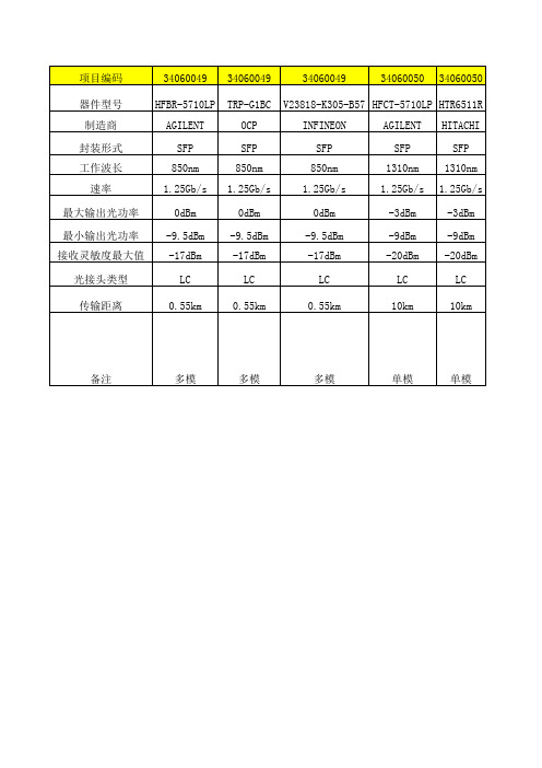
光模块参数1
-7.3~-2.0dBm-8.2~0.5dBm(avg)-8.2~0.5dBm(avg) -11.1dBm SC 最大300m -10.3dBm SC/PC 10km -10.3dBm SC/PC 10km
单模
单模
多模
单模
单模
34120004 TRE5021EN-SW OPNEXT XENPAK 10.3125Gb/s 4*3.125Gb/s 1310nm
3406A005 SXP3101LX SUMITOMO XFP 1310nm
3406A005 TXN181072013X57 862127 INTEL XFP 1310nm
10.3125Gbps/9.953Gbps 10.3125Gbps/9.953Gbps 10.3125Gbps/9.953Gbps 0.5dBm -8.2dBm -12.6dBm LC 10km 0.5dBm -8.2dBm -12.6dBm LC 10km 0.5dBm -8.2dBm -12.6dBm LC 10km
单模
单模
单模
3406A006 JXP-01SWAA1 JDSU XFP 850nm SR/SW -1.08dBm -7.3dBm -11.1dBm LC 300m
3410A000
3410A000
项目编码 器件型号 制造商 封装标准 光口工作速率
3412A000 HFCT-703XBD AGILENT XENPAK 10.3125Gb/s
单模
单模
单模
单模
ቤተ መጻሕፍቲ ባይዱ单模
单模
3406A003
3406A003
3406A003
3406A003
34060287 HFBR-57E0P AGILENT SFP 1310nm STM1 -14dBm -19dBm -30dBm LC (TX disable) 2km
500mA磷酸铁锂电池充电集成电路CN3058

500mA磷酸铁锂电池充电集成电路CN3058概述:CN3058是可以对单节磷酸铁锂电池进行恒流/恒压充电管理的集成电路。
该器件内部包括功率晶体管,不需要外部的电流检测电阻和阻流二极管。
CN3058只需要极少的外围元器件,非常适合于便携式应用的领域。
热调制电路可以在器件的功耗比较大或者环境温度比较高的时候将芯片温度控制在安全范围内。
内部固定的恒压充电电压为3.6V,也可以通过一个外部的电阻调节。
充电电流通过一个外部电阻设置。
当输入电压(交流适配器或者USB电源)掉电时,CN3058自动进入低功耗的睡眠模式,此时电池的电流消耗小于3微安。
其它功能包括输入电压过低锁存,自动再充电,电池温度监控以及充电状态/充电结束状态指示等功能。
CN3058采用8管脚小外形封装(SOP8)。
应用:●矿灯●磷酸铁锂电池应用●各种充电器特点:●独立的单节磷酸铁锂电池充电管理●输入电压范围:3.8V 到 6V●片内功率晶体管●不需要外部阻流二极管和电流检测电阻●恒压充电电压3.6V,也可通过一个外部电阻调节●为了激活深度放电的电池和减小功耗,在电池电压较低时采用小电流的预充电模式●可设置的持续恒流充电电流可达500mA●采用恒流/恒压/恒温模式充电,既可以使充电电流最大化,又可以防止芯片过热●电源电压掉电时自动进入低功耗的睡眠模式●充电状态和充电结束状态双指示输出●C/10充电结束检测●自动再充电●电池温度监测功能●8管脚小外形封装(SOP8)●产品无铅,满足rohs,不含卤素管脚排列:应用电路:图1 典型应用电路(恒压充电电压3.6V)图2 应用电路(利用外接电阻调整恒压充电电压)在图2中,电池正极的恒压充电电压为:Vbat = 3.6+3.61×10⁻⁶×Rx其中,Vbat的单位是伏特Rx的单位是欧姆注:当使用外部电阻调整恒压充电电压时,由于芯片内部和外部的温度不一致及芯片生产时的工艺偏差等原因,可能导致恒压充电电压的精度变差和温度系数变大。
ax3058的规格书

ax3058的规格书全文共四篇示例,供读者参考第一篇示例:AX3058规格书1. 概述AX3058是一款高性能的数字信号处理器,可以广泛应用于音频处理、数字信号处理、通信等领域。
该处理器集成了先进的数字信号处理算法和功率管理模块,具有低功耗、高性能和稳定性的特点。
2. 技术参数- 处理器核心:32位ARM Cortex-M4处理器- 主频:100MHz- 存储器:内置256KB Flash存储器、96KB SRAM- 输入/输出接口:UART、SPI、I2C、USB- 数模转换器:24位高性能ADC/DAC- 功率管理模块:支持多种电源管理模式- 工作电压:1.8V~3.6V- 工作温度:-40℃~85℃3. 特色功能- 高性能:AX3058采用了ARM Cortex-M4处理器核心,主频高达100MHz,能够实现高速的数字信号处理和算法运算。
- 低功耗:该处理器集成了先进的功率管理模块,支持多种低功耗模式,可以有效降低功耗,延长电池寿命。
- 高稳定性:AX3058采用了先进的电路设计和封装工艺,具有优良的抗干扰和抗干扰能力,保证系统稳定性和可靠性。
- 丰富的接口:该处理器支持多种常见的输入/输出接口,如UART、SPI、I2C、USB,方便与外部设备和模块进行通信和连接。
4. 应用领域- 音频处理:AX3058可广泛应用于音频处理领域,如音频编解码、音频滤波等,具有优秀的音频处理性能和音质表现。
- 数字信号处理:该处理器支持多种数字信号处理算法和模块,如滤波、滤波器设计、傅里叶变换等,可应用于数字信号处理系统。
- 通信设备:AX3058具有丰富的接口和通信功能,可用于通信设备的控制、处理和数据传输等。
- 智能家居:该处理器还可应用于智能家居设备中,实现智能控制、传感数据处理等功能。
5. 总结AX3058是一款功能强大、性能稳定的数字信号处理器,具有高性能、低功耗和丰富的接口特点,适用于音频处理、数字信号处理、通信等多个领域。
K系列产品说明书

目录第一章 K系列产品的特点及应用领域 (2)第二章 K3海用信标机 (3)§2.1 信标定位概述 (3)§2.2 K3海用信标机特点及技术参数 (4)§2.3 K3海用信标机硬件介绍 (6)§2.3.1 正面控制面板介绍 (6)§2.3.2 背面接口介绍 (7)§2.3.3 主机侧面介绍 (8)§2.3.4 K3海用信标机附件的介绍 (9)§2.4 K3海用信标机与海洋测量软件的连接 (11)第三章 K5定位定向仪 (21)§3.1 K5海用定位定向仪的特点及技术参数 (21)§3.2 K5定位定向仪硬件介绍 (22)§3.3 K5定位定向仪与海洋测量软件的连接 (24)§3.4 K5定位定向仪与施工定位软件的连接 (28)第四章 K6高精度定向仪 (33)§4.1 K6高精度定向仪特点及技术参数 (33)§4.2 K6高精度定向仪的操作 (34)第五章 K8海用双频RTK (35)§5.1 K8船用双频RTK特点及技术参数 (35)§5.2 K8海用双频RTK硬件介绍 (36)§5.2.1 K8正面板介绍 (36)§5.2.2 K8背面板介绍 (37)§5.2.3 K8附件介绍 (37)§5.3 K8双频RTK与海洋测量软件的连接 (40)1第一章 K系列产品的特点及应用领域根据水上工程施工单位的特殊作业环境和特定需要设计的中海达K系列海用产品,从外观设计到产品内核都是为水上工程单位量身定制,凸显水上作业要求的专业性。
配合中海达的水上软件和测深仪,可更为广泛地使用在水下地形测量,挖泥、炸礁疏浚工程,水底电缆、管道的铺设,跨海大桥的桩位定位等水上工程。
2第二章 K3海用信标机§2.1 信标定位概述信标技术是差分GPS技术的一种,它是利用现有的海用无线电信标台,在其所发射的信号中加一个副载波调制,以发射差分修正信号,提供定位导航服务。
MAX31855热电偶芯片的中文翻译

MAX3855冷端补偿热电偶至数字输出转换器概述MAX31855具有冷端补偿,将K、J、N、T或E型热电偶信号转换成数字量(如果使用S和R 型热电偶,请联系工厂)。
器件输出14位带符号数据,通过SPI TM 兼容接口、以只读格式输出。
转换器的温度分辨率为℃,最高温度读数为+1800℃,最低温度读数为-270℃,对于K型热电偶,温度范围为-200℃至+700℃,保持±2℃精度。
对于整个量程范围的精度及其它类型的热电偶,请参考ThermalCharacteristics 规格。
应用工业电器设备HVAC 汽车特性S 冷端补偿S 14位、℃分辨率S 提供K、J、N、T和E型热电偶器件版本(如果使用S和R型热电偶,请联系工厂) (见表1) S 简单的SPI兼容接口(只读)S 检测热电偶对GND或V CC 短路S 检测热电偶开路典型应用电路SPI是Motorola,Inc.的商标。
对于价格,供货及订购信息,请联络Maxim在2,或访问Maxim的网站。
绝对最大额定值范围电源电压范围(VCC和GND).................. to +所有其他引脚............................................到(V CC+ )连续功率耗散(T A =+70℃)SO(减免℃以上+70℃).......................ESD保护(所有引脚,人体模型).............±2000kV工作温度范围........................-40℃至+125°C连接点温度................................................ .....+150°C存储温度范围..........................-65℃至+150°清除温度(焊接,10秒) (300)焊接温度(回流) (260)强调超出“绝对最大额定值”,即可能对器件造成永久性损坏。
2SK3875-01中文资料

IGSS RDS(on) gfs Ciss Coss Crss td(on) tr td(off) tf QG QGS QGD VSD trr Qrr
Test Conditions ID= 250µA VGS=0V ID= 250µA VDS=VGS
VDS=900V VGS=0V Tch=25°C
10-2
10-3
10-6
10-5
10-4
10-3
10-2
10-1
100
t [sec]
http://www.fujielectric.co.jp/fdt/scd/
4
(Zth(ch-c) [°C/W])
Item Drain-Source Breakdown Voltage Gate Threshold Voltage
Zero Gate Voltage Drain Current
Gate-Source Leakage Current Drain-Source On-State Resistance Forward Transconductance Input Capacitance Output Capacitance Reverse Transfer Capacitance Turn-On Time ton
Applications Switching regulators UPS (Uninterruptible Power Supply) DC-DC converters
Maximum ratings and characteristic
Absolute maximum ratings (Tc=25°C unless otherwise specified)
Min. 900
华为光模块参数
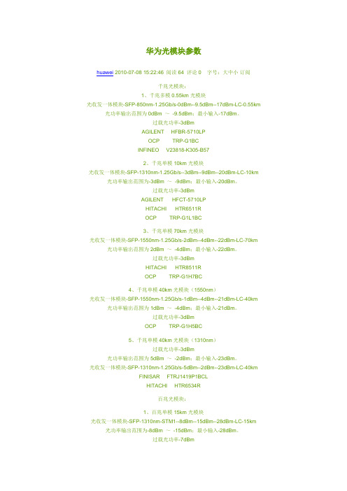
华为光模块参数huawei 2010-07-08 15:22:46 阅读64 评论0 字号:大中小订阅千兆光模块:1、千兆多模0.55km光模块光收发一体模块-SFP-850nm-1.25Gb/s-0dBm--9.5dBm--17dBm-LC-0.55km 光功率输出范围为0dBm ~-9.5dBm;最小输入-17dBm。
过载光功率-3dBmAGILENT HFBR-5710LPOCP TRP-G1BCINFINEO V23818-K305-B572、千兆单模10km光模块光收发一体模块-SFP-1310nm-1.25Gb/s--3dBm--9dBm--20dBm-LC-10km 光功率输出范围为-3dBm ~-9dBm;最小输入-20dBm。
过载光功率-3dBmAGILENT HFCT-5710LPHITACHI HTR6511ROCP TRP-G1L1BC3、千兆单模70km光模块光收发一体模块-SFP-1550nm-1.25Gb/s-2dBm--4dBm--22dBm-LC-70km 光功率输出范围为2dBm ~-4dBm;最小输入-22dBm。
过载光功率-3dBmHITACHI HTR8511ROCP TRP-G1H7BC4、千兆单模40km光模块(1550nm)光收发一体模块-SFP-1550nm-1.25Gb/s-1dBm--4dBm--21dBm-LC-40km 光功率输出范围为1dBm ~-4dBm;最小输入-21dBm。
过载光功率-3dBmOCP TRP-G1H5BC5、千兆单模40km光模块(1310nm)过载光功率-3dBm光功率输出范围为5dBm ~-2dBm;最小输入-23dBm。
光收发一体模块-SFP-1310nm-1.25Gb/s-5dBm--2dBm--23dBm-LC-40kmFINISAR FTRJ1419P1BCLHITACHI HTR6534R百兆光模块:1、百兆单模15km光模块光收发一体模块-SFP-1310nm-STM1--8dBm--15dBm--28dBm-LC-15km 光功率输出范围为-8dBm ~-15dBm;最小输入-28dBm。
E18系列产品规格书说明书
E18系列产品规格书CC25302.4GHz ZigBee3.0无线模块目录第一章产品概述 (3)1.1产品简介 (3)1.2特点功能 (4)1.3应用场景 (5)第二章规格参数 (6)2.1射频参数 (6)2.2电气参数 (6)2.3硬件参数 (6)2.4网络系统参数 (7)第三章机械尺寸与引脚定义 (8)第四章硬件设计 (11)第五章软件设计 (11)第六章常见问题 (13)6.1传输距离不理想 (13)6.2模块易损坏 (13)6.3误码率太高 (13)第七章焊接作业指导 (7)7.1回流焊温度 (7)7.2回流焊曲线图 (7)第八章相关型号 (8)第九章天线指南 (8)第十章产品包装图 (8)修订历史 (9)关于我们 (9)第一章产品概述1.1产品简介E18系列是亿佰特设计生产的2.4GHz频段的ZigBee通信协议转串口无线模块,贴片型,PCB板载天线或IPEX-1接口,引脚间距1.27mm,出厂自带自组网固件,到手即用,适用于多种应用场景(尤其智能家居)。
E18系列模块采用美国德州仪器公司原装进口CC2530射频芯片,芯片内部集成了8051单片机及无线收发器,部分模块型号内置PA功率放大器增加通信距离。
出厂自带固件基于ZigBee3.0协议实现的串口数据透传,支持ZigBee3.0协议下各种指令命令。
经实测,对市面上大多数ZigBee3.0产品有着非常良好的兼容性。
1.2ZigBee 3.0优势E18系列模块固件基于Z-Stack3.0.2协议栈(ZigBee 3.0),该版本为CC2530/CC2538系列芯片最优协议栈,因此我司也此基础上做了许多优化,确保系统长期稳定运行。
ZigBee3.0与早前版本的应用方式区别:1.组网方式发生变化:ZigBee 3.0取缔了一上电就组网的方式,而是根据实际需要进行组网。
任何设备在出厂状态下是无网络状态,协调器需要运行“formation”(调用bdb_StartCommissioning(BDB_COMMISSIONING_MODE_NWK_FORMATION))来新建网络,然后再运行"Steering"(调用bdb_StartCommissioning(BDB_COMMISSIONING_MODE_NWK_STEERING))打开网络,打开网络默认时间180秒,可通过广播"ZDP_MgmtPermitJoinReq"的方式将打开网络提前关闭。
低功耗运算放大器型号说明书

引脚接线图图1. 8引脚MSOP 封装图2. 8引脚LFCSP 封装图3. 输出电压(V OH )至供电轨与负载电流的关系One Technology Way, P.O. Box 9106, Norwood, MA 02062-9106, U.S.A.Tel: 781.329.4700 ©2013 Analog Devices, Inc. All rights reserved.Technical Support Rev. 0Document FeedbackInformation furnished by Analog Devices is believed to be accurate and reliable. However , no responsibility is assumed by Analog Devices for its use, nor for any infringements of patents or other rights of third parties that may result from its use. Speci cations subject to change without notice. No license is granted by implication or otherwise under any patent or patent rights of Analog Devices. T rademarks and registered trademarks are the property of their respective owners.ADI 中文版数据手册是英文版数据手册的译文,敬请谅解翻译中可能存在的语言组织或翻译错误,ADI 不对翻译中存在的差异或由此产生的错误负责。
如需确认任何词语的准确性,请参考ADI 提供的最新英文版数据手册。
W28 二维指环扫描枪 产品规格书说明书

W28二维指环扫描枪产品规格书免责声明请您在使用本手册描述的产品前仔细阅读手册的所有内容,以保障产品的安全有效地使用。
阅读后请将本手册妥善保存以备下次使用时查询。
一旦使用本手册所述产品,即视为您已经仔细阅读免责声明与警告,理解、认可和接受本声明全部条款与内容,您承诺仅出于正当目的使用本产品,对使用本手册所述产品以及可能带来的后果承担相应的责任。
请勿自行拆卸本产品或撕毁产品上的封标,否则浩创科技不承担保修或更换产品的责任。
本手册中的图片仅供参考,如有个别图片与实际产品不符,请以实际产品为准。
本手册包含的所有信息和图片除特别标明之外,版权归浩创科技及其关联公司,未经书面许可,任何单位及个人不得以任何方式或理由对本手册全部或部分内容进行任何形式的摘抄、复制或与其它产品捆绑使用、销售。
本手册所述产品中可能包括浩创科技或第三方享有版权的软件,除非获得相关权利人的书面许可,否则任何单位或者个人不能以任何形式对前述软件进行复制、分发、修改、摘录、反编译、反汇编、解密、反向工程、出租、转让、分许可以及其它侵犯软件版权的行为。
本手册及产品所有相关的文档最终解释权和修改权归浩创科技,如有更新,恕不另行通知,请您访问官方网站或查阅最新版产品手册以获取最新的产品信息。
版本信息目录概述 (4)产品特点 (4)产品优势 (4)产品展示 (4)穿戴方式 (6)充电 (7)通过W2X/SC100充电座进行充电 (7)通过C20充电柜进行充电 (8)更换指环套 (8)指环套安装更换方法 (9)规格参数 (10)指示灯提示 (12)振动提示 (13)景深参数 (15)视场角度 (16)更新扫描枪固件 (17)包装明细 (18)电池安全指南 (19)附录 (20)功能设置条码 (20)通用设置 (20)换行符/制表符 (21)触发方式设置 (22)开启/关闭可识别码制 (23)可识别条码位数设置 (24)前导码输出开关设置 (29)附加码输出开关设置 (29)FULL ASCII开关设置 (30)蓝牙断开报警设置条码 (30)自动间隙出光扫描识别成功后的灭光时间设置 (31)概述除了商超柜台结账扫描目的是为了提取价格信息外,在快递、物流供应链、食品药品溯源管理、智能制造等领域的条码、二维码、RIFD扫描,都只是为了理清责任,起到作业环节转移时的电子签章功能。
CS3818 无电感15W双声道立体声D类音频功率放大器

BSPL
PBTL 选择
OUTPL
OUTNL FB LINP LINN PWM
增益控制
PGND GVDD PVCCL PVCCL
OUTNL FB
PLIMIT
逻辑
BSNL
OUTPLFB
栅驱动
OUTNL
/FAULT /SD MUTE GAIN0 GAIN1 PLIMIT TTL
缓冲器 增益控制 参考基准 上电保护逻辑 温度检测 短路检测 直流检测
版本:S-2016-04-B
第 2 页 共 11 页
M OS 电 路
CS3818
2. 3、引脚排列图
2. 4、引脚说明与结构原理图 引脚 1 符 号 功 能 属性 I /SD 待机逻辑输入,接高电平时通过 100k 接到 AVCC 漏极输出用于显示短路或者直流检测故障,电压接 近 AVCC , 短路故障可以通过连接 /FAULT 和 /SD 引 脚来自动恢复,否则,短路和直流检测故障必须通 过 PVCC 重置 左声道正输入 左声道负输入 增益选择低位,接高电平时通过 100k 接到 AVCC 增益选择高位,接高电平时通过 100k 接到 AVCC 模拟电源 模拟地,连接到散热片 上管栅驱动电压,同时作 PLIMIT 端电源 功率限制电平调整,通过在 GVDD 和 GND 之的电 阻分压来设置限制功率大小;连接到 GVDD 则无 功率限制功能 右声道负输入 右声道正输入 静音逻辑输入,悬空或低电平为电路正常工作,高 电平为静音 , 接高电平时通过 100k 接到 AVCC 并联 BTL 模式开关,接高电平时通过 100k 接到 AVCC 右声道功率电源,左右声道电源输入内部相连
3、 电特性
3. 1 、 极限参数 除非另有规定, T amb = 25℃ 参 数 名 称 电源电压 极限 输入 电压 /SD,GAIN0,GAIN1,PBTL,/FAULTMUTE PLIMIT RINN, RINP, LINN, LINP Tamb Tst g R VIN 符 号 PVCC AVCC 额 定 值 -0.3~30 -0.3~V CC +0.3 –0.3~GVDD+0.3 –0.3~5.3 -40~85 -65~150 > 3.2 ℃ ℃ V 单位 V
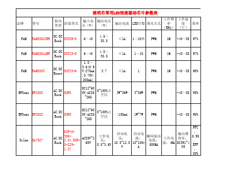
LED恒流驱动IC参数表
PWM
N/A N/A N/A
1M
-40~85 97% -40~85 -40~85 -40~85 -40~85 90% 90% 90% 93% 80% 93%
DC/DC SOT89-5 线性 DC/DC ADDtek AMC7135PKF SOT89-5 线性 DC/DC ADDtek AMC7135PKFA SOT89-5 线性 ADDtek AMC7140DLGT ADDtek AMC7150DLFT ADDtek A711PFT DC/DC TO-252 线性 DC/DC TO-252 Buck DC/DC T0-220 线性 DC/DC TO-263 线性 AC/DC SOT23-5 Buck
应用
PWM
-40~85
93%
ADDtek A704WFT
品牌 ADDtek 型号 AMC7169
85~265
保护电压 (v) 5(MAX)
10~56
保护电流 (mA) 500(MAX)
外置MOS
封装
PWM
65
-40~85
92%
QFN 2mm*2mm 1W灯串中
品牌
ADDtek
型号
AMC720
驱动 封装型式 类型
Maxic
MT7201
7~40 4.5~40
≤38.5 ≤37
≤1A 2A
1~10串 1~10串 12串 *1W/3W
PWM PWM
1M 150
-40~85 97% -40~85 83%
XLSEMI XL4001
XLSEMI XL6003
3.6~36
≤42
2A
PWM
400
-40~105 92%
- 1、下载文档前请自行甄别文档内容的完整性,平台不提供额外的编辑、内容补充、找答案等附加服务。
- 2、"仅部分预览"的文档,不可在线预览部分如存在完整性等问题,可反馈申请退款(可完整预览的文档不适用该条件!)。
- 3、如文档侵犯您的权益,请联系客服反馈,我们会尽快为您处理(人工客服工作时间:9:00-18:30)。
SFP - Small Form-factor PluggableMultimode 850 nm 1.0625 Gbit/s Fibre Channel 1.25 Gigabit Ethernet Transceiver with LC™ ConnectorV23818-K305-B57File: 1114LC™ is a trademark of LucentFiber OpticsFeatures•Small Form-factor Pluggable (SFP) transceiver •Fully SFP MSA compliant 1)•Advanced release mechanism–Easy access, even in belly to belly applications –Grip for easy access – no tool is needed –Color coded black (multimode)•Excellent EMI performance•RJ-45 style LC ™ connector system •Single power supply (3.3 V)•Extremely low power consumption of 415 mW typical •Small size for high channel density •UL-94 V-0 certified•ESD Class 1C per JESD22-A114-B (MIL-STD 883D Method 3015.7)•Compliant with FCC (Class B) and EN 55022•For distances of up to 700 m (50 µm fiber)•Class 1 FDA and IEC laser safety compliant •AC/AC Coupling according to SFP MSA•Recommendation: Infineon Cage one-piece design V23838-S5-N1 for press fit and/or solderable•Operating case temperature: –10°C to 85°C•SFP evaluation board V23818-S5-V2 available upon request1)Current MSA documentation can be found at /fiberopticsPin ConfigurationFigure1SFP Transceiver Electrical Pad LayoutPin DescriptionPin Logic Level Function1V EE T N/A Transmitter Ground1)2Tx Fault LVTTL Transmitter Fault Indication2)8)3Tx Disable LVTTL Transmitter Disable3)4MOD-DEF(2)LVTTL Module Definition 24)8)5MOD-DEF(1)LVTTL Module Definition 15)8)6MOD-DEF(0)N/A Module Definition 06)8)7Rate Select N/A Not connected8LOS LVTTL Loss Of Signal7)8)9V EE R N/A Receiver Ground1)10V EE R N/A Receiver Ground1)11V EE R N/A Receiver Ground1)12RD–LVPECL Inv. Received Data Out9)13RD+LVPECL Received Data Out9)14V EE R N/A Receiver Ground1)15V CC R N/A Receiver Power16V CC T N/A Transmitter Power17V EE T N/A Transmitter Ground1)18TD+LVPECL Transmit Data In10)19TD–LVPECL Inv. Transmit Data In10)20V EE T N/A Transmitter Ground1)1)Common transmitter and receiver ground within the module.2) A high signal indicates a laser fault of some kind and that laser is switched off.3) A low signal switches the transmitter on. A high signal or when not connected switches the transmitter off.4)MOD-DEF(2) is the data line of two wire serial interface for serial ID.5)MOD-DEF(1) is the clock line of two wire serial interface for serial ID.6)MOD-DEF(0) is grounded by the module to indicate that the module is present.7) A low signal indicates normal operation, light is present at receiver input. A high signal indicates the receivedoptical power is below the worst case receiver sensitivity.8)Should be pulled up on host board to V CC by 4.7 - 10 k W.9)AC coupled inside the transceiver. Must be terminated with 100 W differential at the user SERDES.10)AC coupled and 100 W differential termination inside the transceiver.DescriptionThe Infineon Fibre Channel / Gigabit Ethernet multimode transceiver – part of Infineon SFP family – is based on the Physical Medium Depend (PMD) sublayer and baseband medium, type 1000 Base-SX (short wavelength) as specified in IEEE Std 802.3 and Fibre Channel FC-PI (Rev.13) 100-M5-SN-I, FC-PI (Rev.13) 100-M6-SN-I.The appropriate fiber optic cable is 62.5µm or 50µm multimode fiber with LC ™connector.Link Length as Defined by IEEE and Fibre Channel Standards Fiber TypeReachUnitmin.1)1)Minimum reach as defined by IEEE and Fibre Channel Standards. A 0 m link length (loop-back connector) is supported.max.2)2)Maximum reach as defined by IEEE and Fibre Channel Standards. Longer reach possible depending upon link implementation.at 1.0625 Gbit/s 50 µm, 2000 MHz*km 0.5860meters50 µm, 500 MHz*km 0.550050 µm, 400 MHz*km 0.545062.5 µm, 200 MHz*km 0.530062.5 µm, 160 MHz*km 0.5250at 1.25 Gbit/s 50 µm, 500 MHz*km 2550meters50 µm, 400 MHz*km 250062.5 µm, 200 MHz*km 227562.5 µm, 160 MHz*km2220The Infineon SFP multimode transceiver is a single unit comprised of a transmitter, a receiver, and an LC™ receptacle.This transceiver supports the LC™ connectorization concept. It is compatible with RJ-45 style backpanels for high end datacom and telecom applications while providing the advantages of fiber optic technology.The module is designed for low cost SAN, LAN, WAN, Fibre Channel and Gigabit Ethernet applications. It can be used as the network end device interface in mainframes, workstations, servers, and storage devices, and in a broad range of network devices such as bridges, routers, hubs, and local and wide area switches.This transceiver operates at 1.0625Gbit/s / 1.25Gbit/s from a single power supply (+3.3V). The full differential data inputs and outputs are LVPECL compatible. Functional Description of SFP TransceiverThis transceiver is designed to transmit serial data via multimode cable.Figure2Functional DiagramThe receiver component converts the optical serial data into LVPECL compatible electrical data (RD+ and RD–). The Loss Of Signal (LOS) shows whether an optical signal is present.The transmitter converts LVPECL compatible electrical serial data (TD+ and TD–) into optical serial data. Data lines are differentially 100 W terminated.The transmitter contains a laser driver circuit that drives the modulation and bias current of the laser diode. The currents are controlled by a power control circuit to guarantee constant output power of the laser over temperature and aging. The power control uses the output of the monitor PIN diode (mechanically built into the laser coupling unit) as a controlling signal, to prevent the laser power from exceeding the operating limits. Single fault condition is ensured by means of an integrated automatic shutdown circuit that disables the laser when it detects laser fault to guarantee the laser Eye Safety. The transceiver contains a supervisory circuit to control the power supply. This circuit makes an internal reset signal whenever the supply voltage drops below the reset threshold. It keeps the reset signal active for at least 140 milliseconds after the voltage has risen above the reset threshold. During this time the laser is inactive.A low signal on TxDis enables transmitter. If TxDis is high or not connected the transmitter is disabled.The information which kind of SFP module has been plugged into an SFP port can be read through the MOD-DEF interface. The information is stored in an I2C-Eprom inside the SFP Transceiver.Regulatory ComplianceTechnical DataExceeding any one of these values may destroy the device immediately.The electro-optical characteristics described in the following tables are valid only for use under the recommended operating conditions.Absolute Maximum Ratings ParameterSymbolLimit Values Unitmin.max.Package Power Dissipation 0.5W Data Input LevelsV CC +0.5V Differential Data Input Voltage Swing V ID pk-pk5V Storage Ambient Temperature–4085°C V CC max5.5V ECL-Output Current Data50mA Recommended Operating Conditions Parameter SymbolLimit Values Unitmin.typ.max.Case Temperature T C–1085°C Power Supply Voltage V CC –V EE 3.1 3.33.5V TransmitterDifferential Data Input Voltage Swing V ID pk-pk5003200mVReceiverInput Center Wavelengthl C770860nmTransmitter Electro-Optical CharacteristicsTransmitter Symbol Limit Values Unitmin.typ.max.Launched Power (Average)1)P O–9.5–6–4dBm Optical Modulation Amplitude2)OMA156450µW Center Wavelength l C830850860nm Spectral Width (RMS)s I0.85nm Relative Intensity Noise RIN–116dB/Hz Extinction Ratio (Dynamic)ER915dB Total Tx Jitter TJ53130ps Reset Threshold3)V TH 2.5 2.75 2.99V Reset Time Out3)t RES140240560ms Rise Time, 20% - 80%t R260ps Supply Current4565mA1)Into multimode fiber, 62.5 µm or 50 µm diameter.2)Fibre Channel PI Standard.3)Laser power is shut down if power supply is below V TH and switched on if power supply is above V TH after t RES.Receiver Electro-Optical CharacteristicsReceiver Symbol Limit Values Unitmin.typ.max.Sensitivity (Average Power)1)P IN–19.5–17dBm Saturation (Average Power)P SAT0dBm Min. Optical ModulationAmplitude2)OMA1931µWStressed Receiver Sensitivity 50µm Fiber SPIN50µm2455µW3)–17–13.5dB4)Stressed Receiver Sensitivity 62.5µm Fiber SPIN62.5µm3267µW3)–16–12.5dB4)Loss Of Signal (LOS) Assert Level5)PLOSA–30–24dBmLoss Of Signal (LOS) Deassert Level6)PLOSD–22–18dBmLoss Of Signal (LOS) Hysteresis P LOSA–P LOSD 0.52dB Loss Of Signal (LOS)Assert Timet ASS 100µs Loss Of Signal (LOS)Deassert Time t DAS350µs Receiver 3dB Cut-off Frequency 2)1.25 1.5GHz Receiver 10 dB Cut-off Frequency 2)1.53GHz Differential Data Output Voltage Swing 7)V OD pk-pk 5007001230mV Return Loss of Receiver ORL 12dBSupply Current 8)8090mA1)Average optical power at which the BER is 1x10–12. Measured with a 27 –1 NRZ PRBS and ER =9 dB.2)Fibre Channel PI Standard.3)Measured at the given Stressed Receiver Eye Closure Penalty and DCD component given in Fibre Channel PI Standard (2.03/2.18dB & 40/80ps).4)Measured according to IEEE 802.35)An increase in optical power above the specified level will cause the LOS output to switch from a high state to a low state.6)A decrease in optical power below the specified level will cause the LOS to change from a low state to a high state.7)AC/AC for data. Load 50W to GND or 100W differential. For dynamic measurement a tolerance of 50mV should be added.8)Supply current excluding Rx output load.Receiver Electro-Optical Characteristics (cont ’d)ReceiverSymbolLimit Values Unit min.typ.max.Technical DataTiming of Control and Status I/OParameter Symbol Limit Values Unit Conditionmin.max.Tx Disable Assert Time t_off10µs Time from rising edge of TxDisable to when the opticaloutput falls below 10% ofnominal.Tx Disable Negate Time t_on1ms Time from falling edge of TxDisable to when the modulatedoptical output rises above 90%of nominal.Time to Initialize, Including Reset of Tx Fault t_init300From power on or negation ofTx Fault using Tx Disable.Tx Fault AssertTimet_fault100µs Time from fault to Tx Fault on.Tx Disable to Reset t_reset10Time Tx Disable must be heldhigh to reset Tx Fault.LOS Assert Time t_loss_on100Time from LOS state to RxLOS assert.LOS Deassert Time t_loss_off100Time from non-LOS state to RxLOS deassert.I2C Bus Clock Rate f_i2cbus_clock100kHzEye SafetyEye SafetyThis laser based multimode transceiver is a Class 1 product.It complies with IEC 60825-1 and FDA 21 CFR 1040.10 and 1040.11.To meet laser safety requirements the transceiver shall be operated within the Absolute Maximum Ratings.Attention:All adjustments have been made at the factory prior to shipment of thedevices. No maintenance or alteration to the device is required.Tampering with or modifying the performance of the device will result in voided product warranty.Note:Failure to adhere to the above restrictions could result in a modification that isconsidered an act of “manufacturing”, and will require, under law, recertification of the modified product with the U.S. Food and Drug Administration (ref. 21 CFR 1040.10 (i)).Figure 3Required LabelsFigure 4Laser EmissionLaser DataWavelength850 nm Total Output Power(as defined by IEC: 7mm aperture at 14 mm distance)<675µW Total Output Power(as defined by FDA: 7mm aperture at 20 cm distance)<70µW Beam Divergence12°Application Notes EMI-RecommendationsTo avoid electromagnetic radiation exceeding the required limits please take note of the following recommendations.When Gigabit switching components are found on a PCB (multiplexers, clock recoveries etc.) any opening of the chassis may produce radiation also at chassis slots other than that of the device itself. Thus every mechanical opening or aperture should be as small as possible.On the board itself every data connection should be an impedance matched line (e.g.strip line, coplanar strip line). Data, Datanot should be routed symmetrically, vias should be avoided. A terminating resistor of 100 W should be placed at the end of each matched line. An alternative termination can be provided with a 50 W resistor at each (D, Dn). In DC coupled systems a thevenin equivalent 50 W resistance can be achieved as follows:for 3.3 V: 125 W to V CC and 82 W to V EE , for 5 V: 82 W to V CC and 125 W to V EE at Data and Datanot. Please consider whether there is an internal termination inside an IC or a transceiver.In certain cases signal GND is the most harmful source of radiation. Connecting chassis GND and signal GND at the plate/bezel/chassis rear e.g. by means of a fiber optic transceiver/cage may result in a large amount of radiation. Even a capacitive coupling between signal GND and chassis may be harmful if it is too close to an opening or an aperture.If a separation of signal GND and chassis GND is not planned, it is strongly recommended to provide a proper contact between signal GND and chassis GND at every location where possible. This concept is designed to avoid hotspots. Hotspots are places of highest radiation which could be generated if only a few connections between signal and chassis GND exist. Compensation currents would concentrate at these connections, causing radiation.By use of Gigabit switching components in a design, the return path of the RF current must also be considered. Thus a split GND plane of Tx and Rx portion may result in severe EMI problems.The cutout should be sized so that all contact springs of the cage make good contact with the face plate.For the SFP transceiver a connection of the SFP cage pins to chassis GND is recommended. If no separate chassis GND is available on the users PCB the pins should be connected to signal GND. In this case take care of the notes above.Please consider that the PCB may behave like a waveguide. With an e r of 4, the wavelength of the harmonics inside the PCB will be half of that in free space. In this scenario even the smallest PCBs may have unexpected resonances.The SFP transceiver can be assembled onto the host board together with all cages and host board connectors complying with the SFP multi source agreement.Infineon Proposes Figure 5Cage:Infineon TechnologiesHost board connector:Tyco ElectronicsSFPHost board connectorCageFile: 1502Handling NotesFigure6Installing and Removing of SFP-TransceiverEEPROM Serial ID Memory ContentsData Address Hex MSA Name/Description Content/Value003Transceiver type SFP104Extended identifier Serial ID207Connector type LC300Reserved400SONET OC-48500SONET OC-3/12601Gigabit Ethernet720FC reach/technology840FC technology90C FC media1001FC speed1101Encoding120D Nominal bit rate1300Reserved1400Length (9 µm) x 1 km1500Length (9 µm) x 100 m1637Length (50 µm) x 10 m171C Length (62.5 µm) x 10 m1800Length (copper) x 1 m1900Reserved20 - 35Vendor name Infineon AG3600Reserved37 - 39Vendor IEEE OUI00-03-1940 - 55Vendor part number V23818-K305-B5756Vendor revision Infineon production code 57 - 59Vendor revision 1.060 - 61Wavelength8506200Reserved63Check code (0 to 62)6400Reserved651A Transceiver options Tx Disable, Tx Fault, LOS 6669Upper bit rate margin (%)6755Lower bit rate margin (%)68 - 83Vendor serial number84 - 91Vendor date code92 - 94Diagnostic / SFF-8472 compliance Not implemented95Check code (64-94)96 - 12700Vendor specific dataMultimode 850nm Fibre Channel SFP Transceiver, AC/AC TTLFigure7Recommended Host Board Supply Filtering NetworkFigure8Example SFP Host Board SchematicPackage Outlines Package OutlinesFigure9Edition 2003-04-25Published by Infineon Technologies AG,St.-Martin-Strasse 53,D-81541 M ünchen, Germany© Infineon Technologies AG 2003.All Rights Reserved.Attention please!The information herein is given to describe certain components and shall not be considered as warranted characteristics.Terms of delivery and rights to technical change reserved.We hereby disclaim any and all warranties, including but not limited to warranties of non-infringement, regarding circuits, descriptions and charts stated herein.Infineon Technologies is an approved CECC rmationFor further information on technology, delivery terms and conditions and prices please contact your nearest Infineon Technologies Office in Germany or our Infineon Technologies Representatives worldwide.WarningsDue to technical requirements components may contain dangerous substances. For information on the types in question please contact your nearest Infineon Technologies Office.Infineon Technologies Components may only be used in life-support devices or systems with the express written approval of Infineon Technologies, if a failure of such components can reasonably be expected to cause the failure of that life-support device or system, or to affect the safety or effectiveness of that device or system. Life-support devices or systems are intended to be implanted in the human body, or to support and/or maintain and sustain and/or protect human life. If they fail, it is reasonable to assume that the health of the user or other persons may be endangered.For questions on technology, delivery and prices please contact the Infineon Technologies Offices in Germany or the Infineon Technologies Companies and Representatives worldwide: see our webpage at .V23818-K305-B57Revision History:2003-04-25DS1Previous Version:2002-01-28PageSubjects (major changes since last revision)Document completely revised。
